WO2016017522A1 - 分子配線基板 - Google Patents
分子配線基板 Download PDFInfo
- Publication number
- WO2016017522A1 WO2016017522A1 PCT/JP2015/070966 JP2015070966W WO2016017522A1 WO 2016017522 A1 WO2016017522 A1 WO 2016017522A1 JP 2015070966 W JP2015070966 W JP 2015070966W WO 2016017522 A1 WO2016017522 A1 WO 2016017522A1
- Authority
- WO
- WIPO (PCT)
- Prior art keywords
- molecular
- electrode
- spectrum
- peak
- wiring board
- Prior art date
- Legal status (The legal status is an assumption and is not a legal conclusion. Google has not performed a legal analysis and makes no representation as to the accuracy of the status listed.)
- Ceased
Links
- IYGXPQXMSGYBCI-UHFFFAOYSA-N CCCCC(CC)COc(cc(c(OCC(CC)CCCC)c1)C#CSC)c1-c(c(F)c(c(F)c1F)F)c1F Chemical compound CCCCC(CC)COc(cc(c(OCC(CC)CCCC)c1)C#CSC)c1-c(c(F)c(c(F)c1F)F)c1F IYGXPQXMSGYBCI-UHFFFAOYSA-N 0.000 description 1
Images













Classifications
-
- G—PHYSICS
- G01—MEASURING; TESTING
- G01N—INVESTIGATING OR ANALYSING MATERIALS BY DETERMINING THEIR CHEMICAL OR PHYSICAL PROPERTIES
- G01N21/00—Investigating or analysing materials by the use of optical means, i.e. using sub-millimetre waves, infrared, visible or ultraviolet light
- G01N21/62—Systems in which the material investigated is excited whereby it emits light or causes a change in wavelength of the incident light
- G01N21/63—Systems in which the material investigated is excited whereby it emits light or causes a change in wavelength of the incident light optically excited
- G01N21/64—Fluorescence; Phosphorescence
-
- G—PHYSICS
- G01—MEASURING; TESTING
- G01N—INVESTIGATING OR ANALYSING MATERIALS BY DETERMINING THEIR CHEMICAL OR PHYSICAL PROPERTIES
- G01N21/00—Investigating or analysing materials by the use of optical means, i.e. using sub-millimetre waves, infrared, visible or ultraviolet light
- G01N21/62—Systems in which the material investigated is excited whereby it emits light or causes a change in wavelength of the incident light
- G01N21/63—Systems in which the material investigated is excited whereby it emits light or causes a change in wavelength of the incident light optically excited
- G01N21/65—Raman scattering
Definitions
- the present invention relates to a molecular wiring board comprising electrodes arranged on a substrate so as to be spaced apart from each other and molecular chains that bridge between the electrodes so as to allow conduction between adjacent electrodes.
- a molecular device is given as an example of the technology.
- Molecular devices can be more integrated and miniaturized than semiconductor-based devices, and high-order information processing is expected. According to this technology, in addition to such molecular electronics, the realization of molecular sensing is also expected.
- One of the molecular devices includes a substrate, electrodes disposed on the substrate so as to be spaced apart from each other, and a molecular chain that bridges the electrodes so as to allow conduction between adjacent electrodes.
- the concept of so-called molecular wiring boards is well known. In order to achieve this molecular wiring board, a technique for arranging electrodes and molecular chains as desired and a technique for measuring the conductivity between electrodes have been developed.
- Examples of techniques for arranging electrodes and molecular chains as desired include the following methods.
- An infinite number of electrodes can be arranged on the substrate with a predetermined rule by the template method.
- adjacent electrodes can be cross-linked by molecular chains based on polymerization or self-assembly.
- Non-Patent Document 1 discloses an electrode-molecule assembly in which a molecule is sandwiched between a pair of nanogap electrodes so as to bridge the electrodes. Stress is applied to the joined body along the direction in which the electrode pair is separated by an actuator provided with a piezo or the like. As the electrodes are pulled apart, the cross-linked molecules are also pulled away one by one. Along with this, the detected current value also changes stepwise. By collecting the current changes obtained in this way over several thousand times, a conductance histogram is created. Based on this histogram, the conductivity of the molecule can be interpreted.
- Non-Patent Document 2 an electrode-molecule assembly similar to the above is disclosed, and the same stress as described above is applied.
- a Raman spectroscopic analysis of the molecule is performed on the state where the molecule is bonded and the state where the molecule is peeled off. Spectral differences between these states have been confirmed. With this spectral difference, it can be determined whether the molecule is attached to the electrode.
- an object of the present invention is to provide a molecular wiring board capable of obtaining sufficient reliability for evaluation of molecular conductivity in a molecular wiring board as a molecular device.
- the feature of the molecular wiring board according to the present invention is that the substrate, the electrodes spaced apart from each other with a space on the substrate and arranged innumerably with a predetermined rule, and the conduction between the adjacent electrodes among the electrodes.
- a molecular chain composed of a predetermined assembly of molecules that cross-links between the adjacent electrodes so as to allow the above.
- the electrode may have any shape such as a dot shape, a rod shape, or a line shape.
- the distance between the electrodes may be equal, for example, or the distance between the electrodes may be different.
- the electrodes when the shape is a dot shape or a rod shape, for example, the electrodes may be arranged in a lattice shape.
- the electrodes when the shape is a line shape, for example, the electrodes may be arranged so as to be parallel to each other.
- the conduction between the electrodes indicates a predetermined energy conduction, for example, electric conduction or heat conduction.
- the molecular chain joins a part of the predetermined molecule to the electrode after the electrode is disposed on the substrate in order to achieve the cross-linking. It is configured by polymerizing or self-organizing the remaining molecules with the partial molecules as starting and ending points.
- cross-linking of molecular chains is achieved by joining both ends to adjacent electrodes.
- the number of molecular chains between adjacent electrodes may be single or plural.
- the molecular chains may be crosslinked as described below.
- an initiator as a starting point of crosslinking is bonded to the first electrode, and a stopper as a terminal is bonded to the second electrode adjacent to the first electrode.
- a molecular chain may be formed by polymerizing molecules (monomers) from the initiator toward the stopper. That is, a surface initiation reaction (that is, initiation of monomer addition to the initiator) is caused by the initiator bonded to the first electrode, and the molecular chain is grown by sequentially adding monomers from the initiator. .
- a surface termination reaction that is, completion of binding between the terminal monomer and the terminator
- Cross-linking of molecular chains in between is achieved.
- this molecular chain crosslinking method is referred to as a “polymerization start / polymerization stop system”.
- the molecular chain may be crosslinked as follows. First, after an initiator as a starting point of crosslinking is bonded to each of the first and second electrodes, molecules may be grown so as to face each of these initiators to form a molecular chain. That is, a surface initiation reaction is caused by each initiator joined to the first and second electrodes, and a monomer chain is sequentially added from each initiator to grow molecular chains. Thereafter, a surface termination reaction (that is, completion of bonding between monomers at each end) occurs between the ends of the growing molecular chains, thereby achieving cross-linking of the molecular chains between the first and second electrodes.
- this molecular chain crosslinking method is referred to as a “polymerization initiation / growth molecular chain bond termination system”.
- the above crosslinking may be achieved based on self-assembly.
- a molecular chain may be formed so that an initiator as a cross-linking start point is bonded to each of the first and second electrodes and then self-organized from each of these initiators. .
- the molecular wiring board according to the present invention is characterized in that, when the spectroscopic analysis is performed on the predetermined molecule, neither the polymerization nor the self-assembly is started after bonding to the electrode.
- a pre-start spectrum that is a spectrum detected by performing the spectroscopic analysis in a state and a post-start spectrum that is a spectrum detected by performing the spectroscopic analysis after the polymerization or the self-assembly is started Based on the difference, the number of crosslinks of the molecular chain between the adjacent electrodes is determined, and the resistance value detected at both end points of a detection interval that is an interval larger than the interval between the adjacent electrodes; Based on the detection interval and the interval between the adjacent electrodes, a resistance value in the interval between the adjacent electrodes is determined, and the determined number of bridges, Based on the serial determined resistance value is to and determining the conductivity of the molecular chains in the interval of the electrode (claim 1).
- the pre-start spectrum and the post-start spectrum have a group of peaks that are detected by light incident from the light source according to scattering, transmission, absorption, and the like in a predetermined molecule. That is, the spectrum before start and the spectrum after start exhibit a plurality of peak arrangements according to the wave number and wavelength.
- the predetermined difference between the spectrum before the start and the spectrum after the start for example, a change in intensity (height) of a peak included in each spectrum and / or expression of a new peak may be identified as the difference.
- Plural or one peak may be selected from each spectrum for identifying the difference.
- the predetermined difference between the pre-start spectrum and the post-start spectrum changes according to the number of crosslinks of the molecular chain to the electrode.
- the number of crosslinks of molecular chains between adjacent electrodes can be easily and accurately determined based on spectroscopic analysis.
- the resistance value at the interval between adjacent electrodes can also be determined easily and accurately.
- the conductivity of the molecular chain in the electrode spacing can be determined. This conductivity is conductivity (resistance value, electrical conductivity, etc.) per a predetermined number (for example, one) of molecular chains.
- the spectroscopic analysis is Raman spectroscopic analysis or fluorescence spectroscopic analysis
- the pre-start spectrum and the post-start spectrum are obtained when the spectroscopic analysis is the Raman spectroscopic analysis.
- Is a vibration spectrum and when the spectroscopic analysis is the fluorescence spectroscopic analysis, it may be an electronic spectrum (claim 2).
- the predetermined difference in the pre-start spectrum and the post-start spectrum is a peak corresponding to the vibration of the joined molecule in the pre-start spectrum. It may be a difference between the intensity of the peak before start and the intensity of the peak after start which is a peak corresponding to the vibration of the joined molecule in the spectrum after start (Claim 3).
- the pre-start peak and the post-start peak have the same wave number
- the number of crosslinks of the molecular chain is the intensity of the pre-start peak and the post-start peak.
- the larger the difference, the larger the number is determined (claim 4).
- “what has the same wave number” means a peak having the same attribution.
- the molecular chain is formed by polymerizing the molecule, and the post-start spectrum is obtained by performing the Raman spectroscopic analysis after the start of the polymerization and after the completion of the polymerization.
- the pre-start peak and the post-start peak correspond to vibrations of molecules that are bonded to the electrode and terminate the polymerization, and the intensity of the pre-start peak is the peak of the post-start peak. A thing larger than the strength is used (claim 5).
- the peak of interest is derived from a functional group having surface-enhanced Raman scattering (hereinafter referred to as “SERS”) activity in the molecule (for example, initiator) bonded to the electrode.
- SERS surface-enhanced Raman scattering
- This functional group is preferably one that contributes to changes in molecular vibrations before and after initiation based on the surface initiation reaction in the polymerization.
- the pre-start spectrum can be acquired and the SERS peak from this functional group can be acquired as the pre-start peak.
- the after-start spectrum can be acquired, and the after-start peak having the same wave number as the before-start peak can be acquired.
- the SERS peak derived from this functional group has a reduced peak intensity (height) after the start of polymerization as compared to before the start. Accordingly, the intensity (height) of the peak before start is larger than the intensity (height) of the peak after start.
- the reduction ratio of the height corresponds to the ratio of the initiator that has actually started the polymerization with respect to all the initiators joined to the electrode.
- the amount of “total initiator bonded to the electrode” can be obtained separately.
- the absolute amount of “initiator that has actually started polymerization” can be determined. Note that the amount of “total initiator bonded to the electrode” may be acquired using, for example, a photoelectron spectroscopy spectrum. Based on the absolute amount of the “initiator that has actually started polymerization”, the number of crosslinks of the molecular chain between the adjacent electrodes can be determined.
- a peak to be noted in the vibration spectrum for example, it is preferable to pay attention to a peak derived from a functional group having SERS activity in a molecule (for example, a terminator) bonded to the electrode. It is more preferable that this functional group contributes to a change in molecular vibration before and after the start based on the surface termination reaction in the polymerization.
- the pre-start spectrum Prior to the start of polymerization, the pre-start spectrum can be acquired and the SERS peak from this functional group can be acquired as the pre-start peak.
- the post-start spectrum can be acquired, and a post-start peak having the same wave number as the pre-start peak can be acquired.
- the SERS peak derived from this functional group has a reduced peak intensity (height) after completion of polymerization as compared to before the start. Accordingly, the intensity (height) of the peak before start is larger than the intensity (height) of the peak after start.
- the rate of decrease in the peak height corresponds to the ratio of the terminator that actually stopped polymerization with respect to the total terminator bonded to the electrode.
- the amount of “total stopper bonded to the electrode” can be obtained separately.
- the absolute amount of “terminator actually terminated by polymerization” can be determined. Note that the amount of “total stopper bonded to the electrode” may be acquired using, for example, a photoelectron spectroscopy spectrum.
- the absolute amount of the “activator that has actually stopped the polymerization” corresponds to the number of molecular chains that have achieved cross-linking between the electrodes.
- the number of crosslinks of the molecular chain between the adjacent electrodes can be determined. In determining the number of crosslinks of the molecular chain, both the absolute amount of the “actually initiated initiator” and the absolute amount of the “actually terminated initiator” may be used. Only one of them may be used.
- a new SERS peak appears in the vicinity of the peak whose height decreases. This new peak is due to the perturbation of the initiator or terminator due to the monomer addition to the initiator or terminator. In this manner, the appearance of a new peak before and after the start of polymerization may be identified as a predetermined difference in the vibration spectrum.
- the above is the description of the vibration spectrum in the case where the “polymerization start / polymerization stop system” is used.
- the peak of interest is a peak derived from the SERS active functional group of the initiator (bonded to the first and second electrodes), and the peak when using the above “polymerization start / polymerization stop system”. Similar peaks are mentioned. Similarly to the above, this peak also has a reduced peak intensity (height) after the start of polymerization as compared to before the start, and a new SERS peak appears near this peak. In this manner, the change in peak height derived from the initiator functional group and the appearance of a new peak before and after the start of polymerization may be identified as a predetermined difference in the vibration spectrum.
- the reduction ratio of the peak height corresponds to the ratio of the initiator that actually started polymerization with respect to the total initiator bonded to the electrode.
- the amount of “total initiator bonded to the electrode” can be obtained separately. Based on the amount of “total initiator bonded to the electrode” and the above ratio, the absolute amount of “initiator that has actually started polymerization” can be determined. Note that the amount of “total initiator bonded to the electrode” may be acquired using, for example, a photoelectron spectroscopy spectrum.
- the peak to be noted in the vibration spectrum for example, those that contribute to the change in molecular vibration before and after the start based on the surface termination reaction in which the ends of the growing molecular chains are bonded to each other are more preferable.
- the SERS peak derived from this functional group appears as a new SERS peak in the vicinity of the peak where the height decreases.
- the new peak expression before and after the start of polymerization may be identified as a predetermined difference in the vibration spectrum.
- the initiator and stopper bonded to the electrode may be configured as follows.
- the initiator and / or the terminator may have any functional group among ethynyl group, isocyano group, dithiocarbamate group, thiol group, and carbodithiolate group.
- the functional group provided in the initiator and / or the terminator is an ethynyl group or an isocyano group
- the electrode is preferably bonded to carbon in the functional group.
- the functional group is a dithiocarbamate group, a thiol group, or a carbodithiolate group, it is preferable that the electrode is bonded to sulfur in the functional group.
- the molecules constituting the molecular chain are bonded to the side opposite to the site bonded to the electrode.
- the SERS frequency derived from the functional group changes. This is based on the fact that initiators and terminators are perturbed by the molecules that are conjugated.
- the functional groups provided in the initiator and the stopper may be the same or different.
- the functional group bonded to the electrode is capable of stably forming a chemical bond with the electrode material (for example, metal), and a change in the SERS frequency is detected before and after a predetermined process. Anything can be obtained.
- the predetermined process is a process of joining an initiator and / or a stop agent to the electrode, a process of starting polymerization, or a process of stopping polymerization. That is, the functional group that can be employed in the present invention may be other than the functional group group described above as long as this condition is satisfied.
- Examples of the process for joining an initiator and / or a stopper to the electrode include the following.
- a solution containing an initiator and / or a terminator is dropped in a state where the substrate on which the electrodes are disposed is impregnated with a solvent.
- the predetermined functional group with which the initiator and / or the stopper is provided is adsorbed on the electrode surface with a chemical bond.
- the initiator and / or the stop agent are joined to the electrode.
- This peak is attributed to, for example, molecular vibration of the functional group, CH stretching vibration of the aromatic ring, CH out-of-plane bending vibration, vibration of the aromatic ring substituent, and the like.
- the aromatic ring substituent can be a probe.
- the peak intensity after bonding is reduced as compared with that before bonding.
- the reduction rate is theoretically the ratio of the absolute amount of “initiator and / or stopper bonded to the electrode” to the absolute amount of “initiator and / or stopper free in the vicinity of the electrode”. equal.
- a new peak can also appear at a position that was not recognized before joining.
- This peak is attributed to the molecular vibration of the initiator and / or terminator that is perturbed after bonding.
- This peak can be obtained, for example, by performing spectroscopic analysis after rinsing the substrate with a solvent after bonding.
- the absolute amount of “initiator and / or stopper actually bonded to the electrode” can be determined based on the reduction rate described above and the intensity of the newly developed peak.
- the absolute amount of “initiator and / or terminator actually bonded to the electrode” can be quantified, for example, by separately analyzing the electrode substrate.
- Examples of the process for starting the polymerization include the following.
- a solution containing a monomer is dropped in a state where a substrate having an initiator and / or a stopper bonded to the electrode is impregnated with the rinsed solvent.
- polymerization is started from the initiator.
- a vibration spectrum is acquired before and after the start of polymerization.
- a predetermined SERS peak group derived from the initiator bonded to the electrode can be acquired before the start of polymerization.
- the intensity changes at the peak attributed to the functional group related to bonding.
- This peak is attributed to, for example, molecular vibration of the functional group, CH stretching vibration of the aromatic ring, CH out-of-plane bending vibration, vibration of the aromatic ring substituent, and the like.
- This reduction rate is theoretically equal to the ratio of the absolute amount of “actually initiated initiator” to the absolute amount of “total initiator bonded to the electrode”.
- a new peak can also appear at a position that was not recognized before the polymerization was started.
- This peak is attributed to the molecular vibration of the initiator that is perturbed after initiation of polymerization. Based on the above-described reduction rate and the intensity of the newly developed peak, the absolute amount of the initiator that has actually started the polymerization can be determined. With respect to the peak derived from the initiator, the rate of decrease increases with time from the start of the addition of the monomer. Based on the rate of decrease, the polymerization initiation rate can be determined. Note that the peak derived from the terminator remains unchanged until the polymerization proceeds and the polymerization head is bonded to the terminator, that is, until the polymerization is terminated and completed.
- Examples of the process for stopping the polymerization include the following.
- the state in which the substrate is immersed in the solvent as described above is continued.
- the polymerization front end is bonded to the stopper (stopper bonded to the second electrode adjacent to the first electrode bonded to the initiator).
- the polymerization is stopped by the terminator and the polymerization is completed.
- a vibration spectrum is acquired before and after the completion of the polymerization.
- a predetermined SERS peak group derived from the terminator bonded to the electrode can be obtained.
- This peak is attributed to, for example, molecular vibration of the functional group, CH stretching vibration of the aromatic ring, CH out-of-plane bending vibration, vibration of the aromatic ring substituent, and the like.
- This reduction rate is theoretically equal to the ratio of the absolute amount of “stopper actually stopped” to the absolute amount of “total stopper bonded to the electrode”. Actually, it is preferable from the viewpoint of reliability to obtain the above ratio by using the average value of the intensity decrease rate of each peak.
- a new peak can also appear at a position that was not recognized before the completion of the polymerization.
- This peak is attributed to the molecular vibration of the terminator that is perturbed after polymerization is complete. Based on the reduction rate described above and the intensity of the newly appearing peak, the absolute amount of the terminator actually polymerized can be determined. As for the peak derived from the terminator, the rate of decrease increases with time from the start of the monomer addition. Based on the rate of decrease, the polymerization termination rate can be determined.
- an event in which polymerization is initiated by an initiator that is, molecular chain crosslinking is initiated
- an event in which polymerization is completed by a terminator that is, molecular chain crosslinking is completed
- the above quantities can be determined with high reliability.
- the influence of the growing molecules at the front end of the polymerization can also be considered.
- the polymerization tip is sufficiently separated from the electrode surface, and its SERS effect decreases rapidly. For this reason, the peak attributed to the molecular vibration at the polymerization front end is hardly expressed. Therefore, there is almost no need to consider the influence of molecules at the polymerization front end.
- the ratio of the “absolute amount” and the ratio of the “absolute amount of the“ stopper actually stopped ”” to the absolute amount of the “total stopper bonded to the electrode” can be determined with high reliability.
- the polymerization initiation rate and the polymerization termination rate can also be determined with high reliability.
- the absolute amount of the “initiator and / or stopper actually bonded to the electrode” and the above ratio the absolute amount of the “initiator actually started polymerization” in the lift-off, and the touchdown
- the absolute amount of the “activator having actually stopped polymerization” in can be determined with high accuracy.
- the absolute amount of the “termination agent that has actually stopped the polymerization” corresponds to the absolute amount of the molecular chain that bridges between adjacent electrodes. Therefore, this absolute amount is an important value for evaluating the conductivity of the molecular chain per unit number.
- the conductivity of the molecular chain is determined based on the macroscopic gross conductivity of the molecular wiring board, and the process will be described in detail later.
- the molecular chain is formed by polymerizing the molecule, and the molecule that is bonded to the electrode and that is the starting point of the polymerization is a surface initiator.
- a molecule that is bonded to the electrode and that terminates the polymerization is a surface terminator, and the surface initiator and the surface terminator have at least one triple bond between carbon and carbon.
- the electrode is bonded to the electrode via carbon related to the triple bond.
- the number of crosslinks of the molecular chain includes the predetermined difference between the spectrum before the start and the spectrum after the start, and the number of bonds between the surface initiator and / or the surface terminator bonded to the electrode.
- the number of junctions is determined after the disposition of the electrode on the substrate when the spectroscopic analysis is performed on the surface initiator and / or the surface terminator, A pre-bonding spectrum which is a spectrum detected by performing the spectroscopic analysis in a state where neither the surface initiator nor the surface terminator is bonded to the electrode; and the surface initiator and / or the electrode to the electrode A post-bonding spectrum which is a spectrum detected by performing the spectroscopic analysis after the surface terminator has been bonded and the polymerization has not started.
- the molecular chain may be composed of a pi-conjugated polymer (claim 8).
- the initiator and terminator can be a SERS active functional group by providing a triple bond between carbon and carbon, for example. Therefore, according to the above configuration, the change in molecular vibration before and after the start of polymerization (or before and after the completion of polymerization) is large, and the difference between the intensity of the peak before start and the intensity of the peak after start can be large. As a result, the number of crosslinks in the molecular chain can be easily determined.
- the spectroscopic analysis is Raman spectroscopic analysis
- the pre-start spectrum, the post-start spectrum, the pre-join spectrum, and the post-join spectrum are vibration spectra
- the post-start spectrum is the Acquired by performing the Raman spectroscopic analysis after the start of the polymerization and after the completion of the polymerization
- the predetermined difference in the pre-start spectrum and the post-start spectrum is the surface stop in the pre-start spectrum Intensity of the peak before the start corresponding to the vibration of the carbon applied to the triple bond of the agent and the start corresponding to the vibration of the carbon applied to the triple bond of the surface stopper in the spectrum after the start It is the difference from the intensity of the post-peak
- the number of junctions is determined to be larger as the difference in strength
- the following advantages can be obtained by using SERS analysis.
- the intensity of the surface plasmon enhanced electric field in the vicinity of the electrode surface attenuates exponentially along the direction away from the surface.
- the SERS signal derived from the initiator, the stopper, and the inter-electrode molecular chain bonded to the electrode also takes the same attenuation. Therefore, only from the molecular vibration on the electrode surface, the absolute amount of the “actually initiated initiator” and the absolute amount of the “actually terminated initiator” (the number of molecular chains that achieved crosslinking between the electrodes) ) Can be determined easily and accurately.
- a self-assembled monolayer for example, mixed SAM
- the functional groups corresponding to the peak of interest are required to be located at the same distance from the electrode surface.
- the spectroscopic analysis is fluorescence spectroscopic analysis
- an electronic spectrum is used as the predetermined difference in the electronic spectrum.
- a change in light emission before and after the start of polymerization or self-assembly may be identified as the difference.
- This spectroscopic analysis is preferable in the following points.
- initiators and / or terminators modified on the electrode surface these fluorescence intensities can be greatly increased by the surface plasmon enhanced electric field.
- molecular chains (main chain in polymerization) and monomers are separated from the electrodes, and their fluorescence intensity is weak. For this reason, inhibition by the weak fluorescence intensity can be suppressed, and lift-off and / or touchdown can be monitored.
- the “polymerization start / polymerization stop system” it is preferable to pay attention to light emission in the electronic spectrum as follows.
- Examples of light emission to be noticed include those derived from the above initiator (attached to the first electrode). This initiator is based on the surface initiation reaction in the polymerization, (A) quenches after start, (B) shifts the fluorescence spectrum after start, and (C) changes from non-fluorescent to fluorescent after start. Any of these is preferred.
- the initiator is one that is quenched after the start of (A)
- the fluorescence intensity decreases after the start of polymerization as compared to before the start.
- the fluorescence intensity decreases after the start of polymerization compared to before the start.
- the wavelength region of the decreasing fluorescence intensity is the same before and after the start.
- new fluorescence appears in a region different from the wavelength region of the decreasing fluorescence intensity.
- the initiator is changed from non-fluorescent to fluorescent after the start of (C)
- the fluorescence intensity increases after the start of polymerization as compared to before the start.
- the change in emission derived from the initiator before and after the start of polymerization may be identified as a predetermined difference in the electronic spectrum.
- the decrease ratio of the fluorescence intensity in the above (A) and (B) corresponds to the ratio of the initiator that actually started polymerization with respect to the total initiator bonded to the electrode.
- the absolute amount of “initiator that has actually started polymerization” can be determined.
- the amount of “total initiator bonded to the electrode” can be acquired separately, and may be acquired using, for example, a photoelectron spectrum.
- the absolute amount of the “initiator that has actually started polymerization” can be determined by using a calibration curve of the fluorescence intensity of the model molecule measured separately.
- examples of light emission to be noticed in the electronic spectrum include those derived from the terminator (bonded to the second electrode). Based on the surface termination reaction in the polymerization, this terminator (A) quenches after initiation, (B) shifts the fluorescence spectrum after initiation, and (C) changes from non-fluorescent to fluorescent after initiation. Any of these is preferred.
- the terminator quenches after the start of (A)
- the fluorescence intensity decreases after the start of polymerization compared to before the start.
- the terminator is such that the fluorescence spectrum shifts after the start of (B)
- the fluorescence intensity decreases after the start of polymerization compared to before the start.
- the wavelength region of the decreasing fluorescence intensity is the same before and after the start.
- the decrease rate of the fluorescence intensity in the above (A) and (B) corresponds to the ratio of the terminator that actually stopped polymerization with respect to the total terminator bonded to the electrode.
- the absolute amount of “terminator actually terminated by polymerization” can be determined.
- the amount of “total stopper bonded to the electrode” can be acquired separately, and may be acquired using, for example, a photoelectron spectrum.
- the absolute amount of the “stopper that has actually stopped the polymerization” can be determined by using a calibration curve of the fluorescence intensity of the model molecule measured separately.
- the absolute amount of the “activator that has actually stopped the polymerization” corresponds to the number of molecular chains that have achieved cross-linking between the electrodes. Thus, the number of molecular chains that have achieved cross-linking between the electrodes can be determined.
- the above is an explanation of the electronic spectrum when the “polymerization start / polymerization stop system” is used.
- the above-mentioned “polymerization initiation / growth molecular chain bond termination system” it is preferable to pay attention to light emission in the electronic spectrum as follows.
- Examples of light emission to be noticed include those derived from the above initiator (bonded to the first and second electrodes). This initiator is based on the surface initiation reaction in the polymerization, (A) quenches after start, (B) shifts the fluorescence spectrum after start, and (C) changes from non-fluorescent to fluorescent after start. Any of these is preferred.
- the initiator is one that quenches after the start of (A)
- the fluorescence intensity decreases after the start of polymerization compared to before the start.
- the fluorescence intensity decreases after the start of polymerization compared to before the start.
- the wavelength region of the decreasing fluorescence intensity is the same before and after the start.
- new fluorescence appears in a region different from the wavelength region of the decreasing fluorescence intensity.
- the initiator is changed from non-fluorescent to fluorescent after the start of (C)
- the fluorescence intensity increases after the start of polymerization as compared to before the start.
- the change in emission derived from the initiator before and after the start of polymerization may be identified as a predetermined difference in the electronic spectrum.
- the decrease ratio of the fluorescence intensity in the above (A) and (B) corresponds to the ratio of the initiator that actually started polymerization with respect to the total initiator bonded to the electrode.
- the absolute amount of “initiator that has actually started polymerization” can be determined.
- the amount of “total initiator bonded to the electrode” can be acquired separately, and may be acquired using, for example, a photoelectron spectrum.
- the absolute amount of the “initiator that has actually started polymerization” can be determined by using a calibration curve of the fluorescence intensity of the model molecule measured separately.
- examples of light emission that is noticed in the electronic spectrum include those derived from molecular design of molecular chains.
- This molecular design is based on the surface termination reaction in which the ends of the growing molecular chains are bonded to each other, (A) one that newly emits light after the start, or (B) one that the fluorescence spectrum shifts after the start Is preferred.
- the molecular design is such that (A) newly emits light after the start, the fluorescence intensity increases after the start of polymerization compared to before the start.
- the molecular design is such that the fluorescence spectrum shifts after the start of (B)
- the fluorescence intensity decreases after the start of polymerization compared to before the start.
- the wavelength region of the decreasing fluorescence intensity is the same before and after the start.
- new fluorescence appears in a region different from the wavelength region of the decreasing fluorescence intensity.
- the change in emission derived from the terminator before and after the start of polymerization may be identified as a predetermined difference in the electronic spectrum.
- the absolute amount of the “stopper that has actually stopped the polymerization” can be determined by using a calibration curve of the fluorescence intensity of the model molecule measured separately.
- the decrease rate of the fluorescence intensity in the above (B) corresponds to the ratio of the stop agent that actually stopped polymerization with respect to all the stop agents joined to the electrode.
- the absolute amount of “terminator actually terminated by polymerization” can be determined.
- the amount of “total initiator bonded to the electrode” can be acquired separately, and may be acquired using, for example, a photoelectron spectrum.
- the absolute amount of the “activator that has actually stopped the polymerization” corresponds to the number of molecular chains that have achieved cross-linking between the electrodes.
- the number of molecular chains that have achieved cross-linking between the electrodes can be determined.
- the following merits can be obtained by using fluorescence spectroscopy.
- fluorescence spectroscopic analysis on the substrate the intensity of the surface plasmon enhanced electric field near the electrode surface attenuates exponentially along the direction away from the surface.
- fluorescent molecules within a few nanometers from the electrode are efficiently quenched. For this reason, the fluorescence intensity usually decays rapidly after having a maximum value at sub 10 nm. Therefore, in general, the absolute amount of the “initiator that actually started polymerization” using the fluorescence intensity or the absolute amount of the “initiator that actually stopped polymerization” (the number of molecular chains that achieved cross-linking between electrodes). ) Is difficult to determine.
- the conduction characteristics between cross-linked molecules can be obtained with good reproducibility.
- the principle will be described.
- the conduction characteristics strongly depend on the bonding state between the molecules and the electrodes, the number of cross-linked molecular chains, and the like.
- collective evaluation of the conduction characteristics is preferable.
- “collective evaluation” uses a large number of electrodes and considers the conduction path between the electrodes, and evaluates the conduction characteristics between the electrodes (that is, the resistance between the electrodes including a cross-linked molecular chain). It is.
- the collective evaluation involves inhomogeneity in bonding between molecules and electrodes and dispersion of the number of crosslinks in the molecular chain (including wiring defects). In this respect, the collective evaluation is different from the so-called conduction characteristic evaluation using a nanogap electrode.
- a conduction path is formed at an interval sufficiently larger than an interval between adjacent electrodes (hereinafter referred to as “detection interval”).
- detection interval an interval between adjacent electrodes
- the resistance value is defined according to a conduction path through (a molecular chain) between a plurality of electrodes. This conduction path is associated with at least the distance between the electrodes and the resistance value between the adjacent electrodes (molecular chain).
- the resistance value of the detection interval is defined based on the detection distance, the electrode interval, and the resistance value in the electrode interval.
- the resistance value at the electrode spacing can be determined based on the above relationship.
- electrical_connection characteristic per molecular chain can also be determined based on the number of bridge
- the configuration of the molecular wiring board of the present invention is based on such knowledge.
- various conduction paths are formed according to the arrangement of the electrodes.
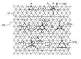
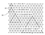
- the electrodes are arranged so that the interval scale between adjacent electrodes is at the nano level, and a triangular lattice is formed when molecular chains are cross-linked to the electrodes.
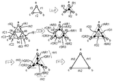
- the conduction path in the molecular wiring board can be regarded as a simplified equivalent circuit using ⁇ -Y conversion and Y- ⁇ conversion (details will be described later). Based on this equivalent circuit, the relationship among the resistance value of the detection interval, the detection distance, the electrode interval, and the resistance value in the electrode interval can be defined by a simple mathematical expression. Therefore, the resistance value between adjacent electrodes can be easily calculated.
- a triangular lattice is formed when the molecular chain is cross-linked to the electrode, and an interval between the adjacent electrodes is arranged.
- the resistance value at is the resistance value detected at both end points of the detection interval, GR , the detection interval is D, the interval between the adjacent electrodes is d, and the resistance value at the interval between the adjacent electrodes is r.
- the coefficient K is determined to shift to a value greater than 0 and less than or equal to 1.
- the coefficient K is adjusted to be a larger value as the detection interval D (the corresponding resistance value) with respect to the size (the corresponding resistance value) of the electrode-arranged substrate is smaller.
- K 1 may be approximated.
- the resistance values detected at both end points of the detection interval are two needle-like probes separated from each other so as to correspond to the detection interval at each tip.
- the resistance value detected by a probe that detects the resistance value corresponding to the distance between the tips by bringing the tips close to the electrode may be used.
- examples of the method for detecting the resistance value with the needle-like probe include the following.
- a macroscopic tester terminal a probe using a microprober for analyzing an electric circuit
- a well-known scanning tunneling microscope a scanning atomic force microscope (cAFM) using a conductive chip, etc. It is not limited to.
- the resistance value at the interval between adjacent electrodes can be obtained easily and reliably. As a result, molecular conductivity with sufficient reliability can be acquired.
- the electrodes are arranged on the substrate using a template having a space corresponding to the shape and the arrangement so that the shape and the arrangement are specified. (Claim 12).
- the template is configured to use a polyethylene oxide-polymethacrylate derivative block copolymer or a polystyrene-poly (4-vinylidylpyridine) block copolymer as a material.
- the electrode uses at least one element of gold, silver, and copper as a material, is configured in a dot shape, and a distance range of an interval between the adjacent electrodes is 5 to 50 nanometers. It is more preferable to be configured to be a meter (claim 13).
- FIG. 2 is a diagram for explaining the introduction of HAuCl 4 in the PEO-b-PMA (Az) film in the electrode placement step according to the molecular wiring board shown in FIG. FIG.
- FIG. 2 is a diagram for explaining a structure of a substrate after removing a PEO-b-PMA (Az) film in an electrode disposing step according to the molecular wiring substrate shown in FIG. 1; It is a flowchart for demonstrating the molecular chain bridge
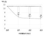
- FIG. 2 is a graph defining the relationship between a coefficient K and a ratio Z 0 / D in a resistance value acquisition step according to the molecular wiring board shown in FIG. It is a figure for demonstrating (DELTA)-> Y conversion and Y-> ⁇ conversion in the resistance value acquisition step concerning the molecular wiring board of the modification of this embodiment. It is a figure for demonstrating the influence of the dispersion
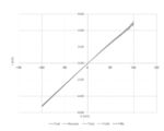
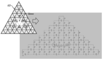
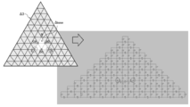
- FIG. 24 It is a figure which shows the simulated molecular wiring board used for verification of resistance value evaluation in the resistance value acquisition step concerning the molecular wiring board of FIG. 24 is a graph showing the relationship between current and voltage corresponding to IV characteristics when the probe arrangement on the simulated molecular wiring board shown in FIG. 23 is the first arrangement. It is a figure which shows the thin wire
- FIG. 2 is a diagram for explaining a resistance network model constructed corresponding to an outer region ⁇ 0 of a basic triangle in the model of the molecular wiring board shown in FIG. 1.
- FIG. 2 is a diagram for explaining a resistance network model constructed corresponding to an outer region ⁇ 1 of a basic triangle in the model of the molecular wiring board shown in FIG. 1.
- FIG. 2 is a diagram for explaining a resistance network model constructed corresponding to an outer region ⁇ 2 of a basic triangle in the molecular wiring board model shown in FIG. 1.
- FIG. 2 is a diagram for explaining a resistance network model constructed corresponding to an outer region ⁇ 3 of a basic triangle in the model of the molecular wiring board shown in FIG. 1. It is a graph which shows the relationship between the gross resistance computed from a resistance network model, and the magnitude
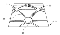
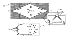
- FIG. 1 is a view showing a molecular wiring board 1 according to an embodiment of the present invention.
- the molecular wiring board 1 includes a substrate 10, an electrode 20, and a molecular chain 30.
- the substrate 10 is a flat plate made of silicon.
- the electrodes 20 each have a dot shape, and are arranged innumerably on the surface of the substrate 10 so as to be spaced apart from each other.
- the material of the electrode 20 is gold, and is disposed by a template method as will be described later.
- the molecular chain 30 bridges between the adjacent electrodes 20 so that conduction between the adjacent electrodes 20 is allowed.
- the molecular chain 30 is formed by polymerization as will be described later.
- FIG. 2 is an enlarged view of the molecular wiring board 1.
- the first electrode 21, the second electrode 22, and the third electrode 23, which are adjacent electrodes 20, are respectively disposed at positions corresponding to vertices on a substantially equilateral triangle. Each spacing is approximately 10 nanometers. That is, the electrode 20 is disposed so that the molecular chains 30 are cross-linked to form a triangular lattice.
- the step includes disposing the electrode 20 on the substrate 10, bridging the disposed electrode 20 with the molecular chain 30, evaluating the degree of crosslinking of the molecular chain 30, and between adjacent electrodes 20 ( That is, this is a step of obtaining a resistance value between any two of the first electrode 21, the second electrode 22, and the third electrode 23).
- these four steps will be described in order as “1. electrode placement step”, “2. molecular chain crosslinking step”, “3. crosslinking evaluation step”, and “4. resistance value acquisition step”, respectively.
- Electrode placement step> First, the step of disposing the electrode 20 on the substrate 10 will be described.
- a template method using the function of an amphiphilic block copolymer is adopted.
- the metal nanoparticles can be regularly arranged on the substrate 10 as the electrode 20 with ultra-high density.
- this block copolymer a polyethylene oxide (PEO) -polymethacrylate derivative (PMA (Az)) copolymer (PEO-b-PMA (Az)) is used.
- PEO-b-PMA (Az) is a side chain liquid crystal type amphiphilic copolymer, and one domain has a function of regularly arranging in many domains. This regular arrangement period is expressed in nano order.
- PEO and PMA (Az) are hydrophilic and hydrophobic, respectively. That is, since each domain has different physical properties, it is easy to modify only one domain.
- the template method is performed from the viewpoint of using the above functions.
- FIG. 3 is a flowchart for explaining the arrangement of the electrodes.
- a film is formed on the surface of the substrate 10.
- the material of the film is the above-mentioned PEO-b-PMA (Az).
- heat treatment is performed.
- a PEO-b-PMA (Az) film is formed on the surface of the substrate 10 with a predetermined thickness.
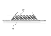
- FIG. 4 is a diagram for explaining the structure of the film formed on the substrate 10.
- the PEO 41 has a cylindrical structure from the substrate 10 along the thickness direction.
- the horizontal cross sections of the plurality of cylindrical PEOs 41 are arranged in a triangular lattice shape (hexagonal lattice shape). That is, the PEO 41 and the PMA (Az) 42 correspond to the one domain and the other domain, respectively.
- the top surface of the cylindrical PEO 41 is exposed on the surface of the PEO-b-PMA (Az) film 40 without being covered with the PMA (Az) 42.
- step 302 an electrode material is introduced into the PEO 41 portion of the PEO-b-PMA (Az) film 40.
- a tetrachloroauric (III) acid aqueous solution (HAuCl 4 ) 43 is dropped onto the surface of the formed PEO-b-PMA (Az) film 40. Thereby, HAuCl 4 43 is introduced from the top surface toward the substrate 10 via the hydrophilic PEO 41.
- FIG. 5 is a diagram for explaining the introduction of HAuCl 4 43 in the PEO-b-PMA (Az) film 40.
- HAuCl 4 43 is dropped on the surface of the PEO-b-PMA (Az) film 40, it is selectively introduced only into the PEO 41 portion. Therefore, gold ions are regularly arranged using the PEO-b-PMA (Az) film 40 as a template. That is, in the PEO-b-PMA (Az) film 40, the HAuCl 4 43 is held only in the cylindrical PEO 41 portion. As a result, the portions where the HAuCl 4 43 is held are arranged in a triangular lattice shape (hexagonal lattice shape).
- step 303 the electrode material is reduced and the PEO-b-PMA (Az) film 40 is removed. Specifically, the vacuum ultraviolet irradiation is performed on the PEO-b-PMA (Az) film 40 in a state where HAuCl 4 43 is introduced into the PEO 41. Thereby, the gold ions at the position corresponding to the PEO 41 are reduced, and the PEO-b-PMA (Az) film 40 is decomposed and removed.
- FIG. 6 is a view for explaining the structure of the substrate after the PEO-b-PMA (Az) film 40 is removed.
- Gold ions located at the position corresponding to the cylindrical PEO 41 are reduced to gold nanoparticles.
- the electrode 20 is disposed so as to correspond to the arrangement of the PEO 41. That is, the electrodes 20 are arranged on the substrate 10 with a period of a triangular lattice shape (hexagonal lattice shape). The above is the description of the steps for disposing the electrode 20 on the substrate 10.
- PEO-b-PMA (Az) is used as the block copolymer in the template method.
- a polystyrene-poly (4-vinylidylpyridine) block copolymer is used. It may be used.
- gold is used as the material of the electrode 20
- silver or copper may be used instead.
- a silver nitrate aqueous solution or a copper nitrate aqueous solution is used as the aqueous solution dropped onto the block copolymer film.
- a material of the electrode 20 it is good also as an alloy using arbitrary 2 combination or all among gold
- a material of the substrate 10 silicon, glass, or the like can be used, but is not limited thereto.
- the electrodes 20 can be arranged at an extremely high density with a very high-grade triangular lattice (hexagonal lattice) structure regularity.
- This electrode arrangement substrate can be mass-produced on a meter scale.
- the molecular chain 30 bridges the adjacent first and second electrodes 21 and 22 so as to allow conduction.
- the molecular chain 30 is composed of an aggregate of predetermined molecules, and the crosslinking is achieved based on polymerization. That is, the cross-linking by the molecular chain 30 between the first and second electrodes 21 and 22 is achieved by the above-described “polymerization start / polymerization stop system”.
- a pi-conjugated polymer is adopted from the viewpoint of ensuring conductivity and forming the molecular chain 30 in a linear shape.
- FIG. 7 is a flowchart for explaining the crosslinking of the molecular chain 30.
- step 701 ⁇ 1.
- the electrode 20 disposed in the electrode disposing step> is surface-modified with an initiator 31 and a stopper 32.
- the initiator 31 and the stopper 32 self-assembled monolayers represented by the following general formulas (1) and (2) are used as the surface initiator and the surface stopper.
- “SiMe 3 ” and “F” represent a trimethylsilyl group and fluorine.
- R any one of deuterium, deuterated acetyl group, deuterated methoxycarbonyl group, and cyano group is used.
- R ′ any one of a deuterated acetyl group, a deuterated methoxycarbonyl group, and a cyano group described later is used. The reason why deuterium is used in this way is to easily distinguish it from other C—H stretching vibrations.
- SERS surface-enhanced Raman scattering
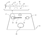
- FIG. 8 is a diagram for explaining the surface modification of the initiator 31 and the stopper 32 to the electrode 20. For simplicity, only a pair of the first electrode 21 and the second electrode 22 will be described.
- the initiator 31 represented by the general formula (1) the ethynyl group at one end and the first electrode 21 are joined by surface modification.
- the stopper 32 also has an ethynyl group at one end thereof bonded to the second electrode 22 by surface modification. Note that surface modification and crosslinking are performed in the same manner in the other electrodes.
- step 702 the polymerization of the molecular chain 30 is started. That is, the monomer is polymerized starting from the initiator 31 bonded to the electrode 20 in Step 701.
- the monomer one represented by the following general formula (3) is used.
- the molecular chain 30 has a unit structure represented by the following general formula (4) and is composed of a pi-conjugated polymer.
- OR (RO) represents an alkyloxy group.
- FIG. 9 is a diagram for explaining how the molecular chain 30 is polymerized. For simplicity, only a pair of the first electrode 21 and the second electrode 22 will be described.
- the pi-conjugated polymer of the general formula (4) grows as a molecular chain 30 starting from the initiator 31.
- the event in which the crosslinking of the molecular chain 30 is initiated (that is, the polymerization is initiated) is referred to as “lift-off”.
- tetrabutylammonium fluoride (TBAF) is used as a catalyst.
- TBAF tetrabutylammonium fluoride
- the first monomer TBAF is used as an anion, and the trimethylsilyl group is eliminated in the presence thereof. By this elimination, the ethynyl group becomes an ethynyl anion.
- the pentafluorophenyl group of the second monomer is bonded to the ethynyl anion in the first monomer.
- This bond is formed at the 4-position carbon site of the pentafluorophenyl group.
- the fluorine originally bonded to the 4-position carbon site is eliminated and a fluoride anion is newly generated.
- the trimethylsilyl group of the second monomer is eliminated by the newly generated fluoride anion.
- This process is sequentially repeated to polymerize, and as a result, a pi-conjugated polymer represented by the unit structure of the general formula (4) is constructed.
- a surface initiation reaction is caused by the TBAF catalyst and the monomer represented by the general formula (3).
- the lift-off is achieved. That is, at the initiator 31 having one end bonded to the first electrode 21, the trimethylsilyl group at the other end is eliminated, and the other end side ethynyl group of the initiator 31 and the 4-position carbon of the monomer pentafluorophenyl group are Join.
- the molecular chain 30 of the general formula (4) grows.
- step 703 the polymerization of the molecular chain 30 is completed. That is, the polymerization is completed by terminating the stopper 32 bonded to the electrode 20 in Step 701.
- FIG. 10 is a diagram for explaining a state in which the polymerization of the molecular chain 30 is completed. For simplicity, only a pair of the first electrode 21 and the second electrode 22 will be described. When the end of the growing molecular chain 30 reaches the stopper 32, the growth of the molecular chain 30 is stopped simultaneously with the binding to the stopper 32. The event in which the crosslinking of the molecular chain 30 is completed (that is, the polymerization is completed) is referred to as “touchdown”.
- the self-assembled monolayers represented by the general formula (1) and the general formula (2) are used as the initiator 31 and the stop agent 32.
- the following general formula (5) and the following general formula (6) may be used.
- N represents nitrogen.
- the monomer of the general formula (3) and the pi-conjugated polymer represented by the unit structure of the general formula (4) were used, but instead of this, other monomers and A unit structure may be used.
- a monomer represented by the following general formula (7) may be used, and the molecular chain 30 may be represented by a unit structure represented by the following general formula (8).
- “O”, “S”, and “Bu” represent oxygen, sulfur, and butyl groups, respectively.
- a monomer represented by the following general formula (9) may be used, and the molecular chain 30 may be represented by a unit structure represented by the following general formula (10).
- a monomer represented by the following general formula (11) may be used, and the molecular chain 30 may be represented by a unit structure represented by the following general formula (12).
- a monomer represented by the following general formula (13) may be used, and the molecular chain 30 may be represented by a unit structure represented by the following general formula (14).
- a monomer represented by the following general formula (15) may be used, and the molecular chain 30 may be represented by a unit structure represented by the following general formula (16).
- the “polymerization start / polymerization stop system” is used as a method for crosslinking the molecular chain 30.
- the “polymerization start / growth molecular chain bond stop system” is used. Also good.
- an initiator 31 as a cross-linking start point is bonded to each of the first and second electrodes 21 and 22, and then molecules are grown so as to face each of the initiators 31, thereby generating molecular chains. 30 may be formed. That is, a surface initiation reaction is caused in each initiator 31 joined to the first and second electrodes 21 and 22, and a monomer is sequentially added from each initiator 31 to grow each molecular chain 30. Thereafter, a surface termination reaction occurs between the ends of the molecular chains 30 that are grown, thereby achieving cross-linking of the molecular chains between the first and second electrodes 21 and 22.
- the above crosslinking may be achieved based on self-assembly.
- the molecular chain 30 is formed so that the initiator 31 as the starting point of the cross-linking is bonded to each of the first and second electrodes 21 and 22 and then self-assembled from each of the initiators 31. May be formed.
- Crosslinking evaluation step> Next, the step of evaluating the degree of crosslinking of the molecular chain 30 crosslinked to the electrode 20 will be described. In this step, the lift-off amount and the touch-down amount are quantified using SERS. This quantitative method is based on the following knowledge. ⁇ 1.
- the electrode 20 obtained in the electrode disposing step> is disposed as gold nanoparticles at an ultra-high density. For this reason, a large SERS gain is obtained by the surface plasmon enhanced electric field for this group of electrodes 20. In obtaining this SERS gain, a general-purpose Raman scattering device can be used. On the other hand, the above-described enhanced electric field has a tendency to attenuate rapidly according to the distance away from the surface. Based on these, ⁇ 2.
- the molecular chain crosslinking step it is possible to easily and sensitively track each change in electronic state (ie, change in molecular vibration due to bonding) accompanying surface modification, lift-off, and touchdown on the electrode 20.
- FIG. 11 is a flowchart for explaining quantification using SERS.
- the quantification using this SERS is the above-mentioned ⁇ 1. After the electrode disposing step>, ⁇ 2. It is appropriately introduced during the molecular chain crosslinking step> (that is, during the “polymerization start / polymerization stop system”).
- the same steps as those shown in FIG. 7 described above are designated by the numbers corresponding to those steps, and the description is omitted.
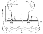
- a Raman spectrum is obtained for the substrate obtained in the above-described “1. electrode placement step” before surface modification. Specifically, the Raman spectroscopic analysis is performed in a state where the substrate 10 provided with the electrode 20 is impregnated with a solvent, added, and a solution containing the initiator 31 and the stopper 32 is dropped. That is, this Raman spectroscopic analysis is performed in a state before joining to the electrode 20 (before surface modification).
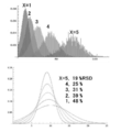
- FIG. 12 is a diagram for explaining a part of the acquired Raman spectrum.
- the spectrum acquired in step 1101 is indicated by a solid line.
- the initiator 31 and the terminator 32 are liberated in the vicinity of the electrode 20, and the above-mentioned spectrum includes peaks derived therefrom.
- the intensity (height) at these peaks corresponds to the state where the initiator 31 and the stopper 32 are not joined to the electrode 20.
- the peak is selected as follows. As the peak derived from the initiator 31, a peak attributed to the triple bond of the ethynyl group carbon at the end of the initiator 31 is selected. As the peak derived from the terminator 32, a peak attributed to the triple bond of ethynyl group carbon at the end of the terminator 32 is selected.
- the intensity (height) corresponding to each selected peak is referred to as “pre-bonding initiator peak intensity I i ” and “pre-bonding stopper peak intensity I f ”, respectively.
- Step 701 after the surface of the electrode 20 is modified with the initiator 31 and the stopper 32 described above, the process proceeds to Step 1102 and a Raman spectrum is acquired for the substrate after the surface modification. Specifically, after a predetermined time has elapsed from the state in step 1101, the Raman spectroscopic analysis is performed again in a state where the substrate is rinsed with a solvent. That is, this Raman spectroscopic analysis is performed in a state after bonding to the electrode 20 (after surface modification).
- the spectrum acquired in step 1102 is indicated by a broken line in FIG.
- An initiator 31 and a stopper 32 are joined to the first and second electrodes 21 and 22, and the spectrum includes peaks derived from these.
- the intensity (height) at these peaks corresponds to the state in which the initiator 31 and the stopper 32 are joined to the electrode 20.
- the initiator 31 and the stopper 32 contained in the solvent are roughly classified into those that are joined and those that are not joined.
- the intensity of the peak selected as described above decreases by an amount corresponding to the amount of junction.
- the intensity of the broken line peak at this time is the post-joining initiator peak intensity I ′ i ( ⁇ I i ) and the post-joining stopper peak intensity I ′ f ( ⁇ I f ). These peak intensities are equivalent to the amounts of initiator 31 and stop agent 32 that have not been joined.
- a new peak appears at a wave number shifted from the solid line peak.
- the change between the spectrum before bonding (solid line, step 1101) and the spectrum after bonding (dashed line, step 1102) is that they are bonded to the electrode 20 in the initiator 31 and the stopper 32.
- the intensity of the new peak is theoretically I i -I ′ i and I f -I ′ f for the initiator 31 and the stopper 32, respectively.
- the intensity of the new peak is actually smaller than those values.
- the peak intensity reduction rate in the initiator 31 and the stop agent 32 is set. Specifically, the reduction rate ⁇ of the post-joining initiator peak intensity I ′ i with respect to the pre-joining initiator peak intensity I i is set. In addition, a reduction rate ⁇ of the post-bonding stopper peak intensity I ′ f with respect to the pre-bonding stopper peak intensity I f is set. The decrease rate ⁇ and the decrease rate ⁇ are set based on I i , I ′ i , I f , I ′ f acquired in steps 1101 and 1102, and the following equations (17) and (18).
- the reduction rate ⁇ corresponds to the ratio of the absolute amount of “initiator 31 bonded to electrode 20” to the absolute amount of “initiator 31 released in the vicinity of electrode 20”.
- the reduction rate ⁇ corresponds to the ratio of the absolute amount of “stopper 31 bonded to electrode 20” to the absolute amount of “stopper 31 released in the vicinity of electrode 20”.
- step 1104 it progresses to step 1104 and acquires the surface modification amount of the initiator 31 and the terminator 32 before the polymerization starts.
- the initiator surface modification amount n i0 that is the absolute amount of the “initiator 31 bonded to the electrode 20”.
- the stop agent surface modification that is the absolute amount of the “stop agent 32 bonded to the electrode 20”.
- the quantity n f0 is obtained.
- Various chemical analyzes can be used to detect the absolute amounts of the initiator 31 and the stop agent 32. For example, inductively coupled plasma (ICP) analysis is preferably used.
- ICP inductively coupled plasma
- the relationship between the above I i , I ′ i , ⁇ and the initiator surface modification amount n i0 may be defined in advance.
- the relationship between the above I f , I ′ f , ⁇ and the stopper surface modification amount n f0 may be defined in advance.
- the alkylthiol when the alkylthiol is added, all of the initiator 31 and the stopper 32 bonded to the electrode 20 are detached from the electrode substrate, and the alkylthiol is bonded to the electrode 20 instead.
- the amount of the initiator 31 and the terminator 32 desorbed is the amount of the initiator 31 (initiator surface modification amount n i0 ) and the amount of the terminator 32 (terminator surface modification amount n f0 ) bonded to the electrode 20. ) Is equivalent. Therefore, the initiator surface modification amount n i0 and the stop agent surface modification amount n f0 are respectively acquired by acquiring the amounts of the detached initiator 31 and stop agent 32 in the electrode substrate.
- a calibration curve is acquired using the acquired n i0 and n f0 and the quantities (I i , I ′ i , ⁇ , and I f , I ′ f , ⁇ ) corresponding to them.
- step 1105 the process proceeds to step 1105 to obtain a Raman spectrum (corresponding to the spectrum before start).
- Raman spectroscopic analysis is performed on the initiator 31 and the stopper 32 bonded to the electrode 20. That is, this Raman spectroscopic analysis is performed after joining to the electrode 20 and in a state where polymerization is not started.
- FIG. 13 is a diagram for explaining a part of the acquired Raman spectrum.
- the spectrum acquired in step 1105 is indicated by a solid line.
- This spectrum includes a peak derived from the initiator 31 and a peak derived from the stopper 32.
- the intensity (height) at these peaks corresponds to a state in which nothing other than the initiator 31 and the stopper 32 is joined to the electrode 20 before the start of polymerization.
- the peak is selected as follows.
- a peak (initiator ⁇ C ⁇ C peak) attributed to the triple bond of ethynyl group carbon on the side of the initiator 31 bonded to the first electrode 21 is selected.
- a peak (terminator ⁇ C ⁇ C peak) belonging to the triple bond of ethynyl group carbon on the side of the terminator 32 bonded to the second electrode 22 is selected.
- the intensity (height) corresponding to each selected peak is referred to as “initiator peak intensity I pi before polymerization initiation” and “stop initiator peak intensity I pf before polymerization initiation”, respectively.
- step 1106 the process proceeds to step 1106 to obtain a Raman spectrum (corresponding to the spectrum after the start).
- Raman spectroscopic analysis is performed on the initiator 31 and the stopper 32 bonded to the electrode 20. That is, the Raman spectroscopic analysis is performed after the polymerization is started and in a state where the polymerization is completed.
- the spectrum acquired in step 1103 is indicated by a broken line.
- This spectrum also includes a peak derived from the initiator 31 and a peak derived from the stopper 32.
- the strength (height) at these peaks corresponds to the state in which the monomer of the general formula (1) is bonded to the initiator 31 and the stopper 32 after the polymerization is started and after the polymerization is completed.
- the initiator ⁇ C ⁇ C peak and the stopper ⁇ C ⁇ C peak are selected in this spectrum.
- the intensities (heights) corresponding to the selected peaks are referred to as “post-polymerization initiator peak intensity I ′ pi ” and “post-polymerization initiator peak intensity I ′ pf ”, respectively.
- the intensity of the initiator ⁇ C ⁇ C peak decreases by an amount corresponding to the amount of lift-off.
- the intensity of the broken line peak at this time is the initiator peak intensity I ′ pi ( ⁇ I pi ) after the initiation of polymerization. This peak intensity is equivalent to the amount of initiator 31 for which lift-off has not been achieved.
- a new peak appears at a wave number shifted from the solid line peak. This new peak has an intensity corresponding to the amount of lift-off.
- the intensity of the stop agent ⁇ C ⁇ C peak decreases by an amount corresponding to the amount of touchdown.
- the intensity of the broken-line peak at this time is the above-described after-polymerization stopper peak intensity I ′ pf ( ⁇ I pf ). This peak intensity is equivalent to the amount of stop agent 32 for which touchdown has not been achieved.
- a new peak appears at a wave number shifted from the solid line peak. This new peak has an intensity corresponding to the amount of touchdown.
- the change between the spectrum before the start of polymerization (solid line, step 1105) and the spectrum after the completion of polymerization (broken line, step 1106) is the same for the initiator 31 and the stop agent 32 as in the general formula (1 ) Is added based on the fact that the perturbation mode of the ethynyl group changes from before the addition.
- the intensity of the new peak is theoretically I pi ⁇ I ′ pi and I pf ⁇ I ′ pf for the initiator 31 and the stopper 32, respectively. However, the intensity of the new peak is actually smaller than those values.
- the rate of decrease in peak intensity in the initiator 31 and the stop agent 32 is set. Specifically, the rate of decrease ⁇ of the initiator peak intensity I ′ pi after the start of polymerization with respect to the initiator peak intensity I pi before the start of polymerization is set. In addition, a reduction rate ⁇ of the stopper peak intensity I ′ pf after the start of polymerization is set with respect to the peak intensity I pf of the stopper before the start of polymerization.
- the decrease rate ⁇ and the decrease rate ⁇ are set based on I pi , I ′ pi , I pf , I ′ pf acquired in steps 1105 and 1106, and the following expressions (19) and (20).
- the reduction rate ⁇ corresponds to the ratio of the absolute amount of “the initiator 31 that has actually started polymerization” to the absolute amount of “the total initiator 31 bonded to the electrode 20”.
- the reduction rate ⁇ corresponds to the ratio of the absolute amount of “the stopper 32 actually stopped for polymerization” to the absolute amount of “the total stopper 32 bonded to the electrode 20”.
- step 1108 the process proceeds to step 1108, and the amount of the initiator 31 that has actually been lifted off from the initiator 31 is acquired.
- the amount of the stop agent 32 in which the touchdown is actually achieved is acquired.
- These amounts are referred to as “lift-off amount n i1 ” and “touch-down amount n f1 ”, respectively (the lift-off amount and / or the touch-down amount correspond to the number of bridges between adjacent electrodes).
- the lift-off amount n i1 is acquired based on the peak attributed to C ⁇ C on the first electrode 21 side of the initiator 31, but in addition to this, C ⁇ C on the SiMe 3 side It may also be based on the peak attributed to. Further, the lift-off amount n i1 may be acquired based only on the peak attributed to C ⁇ C on the SiMe 3 side.
- a peak for obtaining the lift-off amount n i1 and the touch-down amount n f1 a peak attributed to C ⁇ C of the initiator 31 and a peak attributed to C ⁇ C of the stopper 32 are selected.
- peaks of functional group assignments corresponding to R of the initiator 31 (the above general formula (1)) and R ′ of the stopper 32 (the above general formula (2)) may be selected.
- both the lift-off amount n i1 and the touch-down amount n f1 are acquired in order to evaluate the degree of crosslinking of the molecular chain 30, but instead, the lift-off amount n i1 and the touch-down amount Only one of the quantities n f1 may be acquired.
- Raman spectroscopic analysis is used when acquiring a spectrum, but instead of this, for example, X-ray photoelectron spectroscopic analysis may be used.
- Resistance value acquisition step> Next, the step of acquiring the resistance value between the adjacent electrodes 20 will be described.
- the number of the electrodes 20 is a large number, and the interval thereof is on the nanometer level. Therefore, the above-described “collective evaluation” can be used to evaluate the conduction characteristics of the substrate. Thereby, the nonuniformity in the joining of the molecular chain 30 and the electrode 20 and the dispersion of the number of crosslinks of the molecular chain 30 can be incorporated into the evaluation.
- FIG. 14 is a schematic diagram showing a group of electrodes 20 in which molecular chains 30 are cross-linked.
- This schematic diagram corresponds to FIG. 1 described above, and shows a state in which the arrangement of the electrode 20 and the crosslinking of the molecular chain 30 are ideally performed.
- the ideal state is a state in which the dots of each electrode 20 have the same size and are arranged at equal intervals.
- each molecular chain 30 is linearly cross-linked with the same length, one between each electrode 20.
- a perfect triangular lattice is formed at any location.
- the actual electrode 20 and molecular chain 30 do not necessarily form a complete triangular lattice. For this reason, nonuniformity in joining of the molecular chain 30 and the electrode 20 and dispersion of the number of crosslinks of the molecular chain 30 occur.
- ⁇ ⁇ Y conversion and Y ⁇ ⁇ conversion are used for defining the conduction path.
- FIG. 15 is a diagram for explaining ⁇ ⁇ Y conversion and Y ⁇ ⁇ conversion in the molecular wiring board according to the present embodiment. Attention is focused on one minimum unit triangular lattice. This triangular lattice can be regarded as a ⁇ element in the ⁇ ⁇ Y conversion. In the ⁇ element, the resistance of the molecular chain 30 that bridges the electrodes a, b, and c (resistance between one electrode) is r. That is, “r” indicates an average resistance in the ⁇ element. This value corresponds to the resistance value R 1, which will be described later.
- a lattice in which one side of the ⁇ element corresponds to three electrodes 20 minutes, which is one triangular lattice on the substrate.
- the electrodes ab, bc, ca are located in the middle of each side. These intermediate electrodes ab, bc, and ca also form a path for mutual conduction.
- the above-described ⁇ ⁇ Y conversion is performed for each ⁇ element constituted by three electrodes a, ab, ca, three electrodes b, ab, bc, and three electrodes c, ca, bc. To do. Thereby, a resistance value of (1/3) r is obtained in each Y element.
- a new ⁇ element appears as an equivalent circuit.
- One side of the ⁇ element is (2/3) r.
- ⁇ ⁇ Y conversion is performed on the newly expressed ⁇ element.
- the same three virtual paths as described above from the relationship between r and R, resistance is (2/9) r).
- These three virtual paths are extended to the electrodes a, b, and c, respectively. Therefore, a new Y element connected from the center of the ⁇ element to the electrodes a, b, and c appears.
- Y ⁇ ⁇ conversion is performed on the newly expressed Y element. That is, when attention is paid to the ⁇ element having the vertices of the electrodes a, b, and c, the resistance value on one side is (5/3) r from the relationship of r and R. This value corresponds to a resistance value R 2 described later.
- R X is a diagram for explaining the resistance value R X of one side in the ⁇ element.
- FIG. 17 is a diagram for explaining the collective evaluation of the resistance value between the electrodes 20 in the molecular wiring board according to the present embodiment. Attention is paid to four electrodes A, B, C and D which are electrodes 20 arranged at the end of the substrate 10 and sufficiently separated from each other. The distance between these electrodes 20 is sufficiently larger than the distance between adjacent electrodes 20. In the four electrodes A, B, C, and D, two triangular lattices (that is, ⁇ elements) are formed by the three electrodes A, B, and C and the three electrodes A, B, and D. The conduction path connecting the electrodes A and B is assumed to share one side of the two triangular lattices.
- a probe is inserted in the middle of a conduction path connecting electrodes A and B.
- This probe is two needle-like probes spaced apart from each other at the tips P1 and P2.
- a resistance value (a gloss resistance GR described later) corresponding to the interval between the tips is detected.
- the distance D between the probe tips P1 and P2 (corresponding to the electrode 20) is sufficiently larger than the distance between adjacent electrodes, and is between the electrodes AB, BC, CA, BD And sufficiently smaller than the interval corresponding to the path between D and A.
- FIG. 18 is a diagram for describing detection of a resistance value using two needle-like probes P.
- the two needle-like probes P are arranged such that their tips P1 and P2 have a predetermined interval. This predetermined interval is defined as interval D (corresponding to detection interval D).
- a current is output toward the needle-like probe P.
- This current is variably controlled within a predetermined range. Therefore, by connecting the probe tips P1 and P2 to the electrode 20 as described above, a controlled current is conducted through P1 and P2.
- a resistance value (gross resistance GR ) is determined based on the slope of the IV characteristic.
- the gross resistance GR is detected by a so-called two-terminal method.
- the two-terminal method is used for detecting the resistance value. Instead, for example, a four-terminal method may be used.
- an equivalent circuit is configured with the probe tips P1 and P2 as detection points.
- seven types of routes are defined between P1-A, between P2-B, between P1-P2, between AC, between CB, between BD, and between DA.
- the rank of the ⁇ element corresponding to each path is P, Q, L, and M, N X and resistance value R X in each path are respectively expressed as follows based on the above equation (22).
- the gross resistance detected at each of the probe tips P1 and P2 is GR
- the above-described R P , R Q , R L , and R M are used, and the gross resistance GR is expressed by the following equation (23) from an equivalent circuit. expressed.
- the resistance values R P , R Q , R L , and R M are defined by the relationship represented by the following formula (24).
- 1 / GR 1 / RL + 1 / ( RP + RQ + RM ) (23)
- R M R P + R Q + R L (24)
- the formula (23) can be transformed into the following formula (26) by using the formula (24).
- the coefficient K is a value represented by the following equation (27).
- the resistance at the adjacent electrodes 20 can be easily determined.
- the resistance value r determined in this way is an average resistance value between the adjacent electrodes, and the nonuniformity at the junction between the molecular chain 30 and the electrode 20 and the dispersion of the number of crosslinks of the molecular chain 30 are introduced. It can be a thing. Therefore, the conduction characteristics can be determined with good reproducibility in the molecular chain 30 bridged between the adjacent electrodes 20. This is equivalent to obtaining an effective resistance value in the adjacent electrode 20.
- the conductivity per unit molecular chain 30 can also be evaluated by using the lift-off amount and touchdown amount (number of cross-links of the molecular chain 30) determined in the crosslinking evaluation step>. Assuming that the resistance value and electrical conductivity per molecular chain between adjacent electrodes are single r and single s, these are determined from the following formula (33), the following formula (34), and the above formula (31). Can be determined based on the resistance value r and the touchdown amount n f1 determined from the above equation (21). Note that the lift-off amount n i1 may be used instead of the touch-down amount n f1 (see the above formula (20)).
- the determination of the resistance value r in the present embodiment is made on the assumption that the resistance value r corresponding to each side is the same in the triangular lattice constituted by the electrodes 20.
- the resistance values corresponding to each side of the ⁇ element may be different.
- the conduction path can be defined based on ⁇ ⁇ Y conversion and Y ⁇ ⁇ conversion of the resistance value.
- ⁇ ⁇ Y conversion and Y ⁇ ⁇ conversion when resistance values corresponding to each side of the ⁇ element are different will be described.
- FIG. 21 is a diagram for explaining ⁇ ⁇ Y conversion and Y ⁇ ⁇ conversion in the molecular wiring board according to the modification of the present embodiment.
- This FIG. 21 corresponds to FIG. 15 described above, and the description of the common parts / calculations is omitted by using the one in FIG. Attention is paid to a triangular lattice of the minimum unit, which is one triangular lattice on the substrate 10.
- the resistances of the molecular chains that bridge the electrodes ab, bc, and ca are r1, r2, and r3, respectively.
- ⁇ ⁇ Y conversion is performed on this ⁇ element, a Y element is obtained.
- the resistances corresponding to the virtual path in the Y element are R1, R2, and R3, respectively.
- R1 r3r1 / (r1 + r2 + r3)
- R2 r1r2 / (r1 + r2 + r3)
- R3 r2r3 / (r1 + r2 + r3)
- the resistances of the molecular chains that bridge the electrodes a-ab, ab-ca, and ca-a are rA1, rA2, and rA3, respectively ( ⁇ element A).
- the resistances of the molecular chains that bridge the electrodes ab-b, b-bc, and bc-ab are rB1, rB2, and rB3, respectively ( ⁇ element B).
- the resistances of the molecular chains that bridge the electrodes ca-bc, bc-c, and c-ca are rC1, rC2, and rC3, respectively ( ⁇ element C).
- ⁇ element A, ⁇ element B, and ⁇ element C Y element A, Y element B, and Y element C corresponding to each are obtained.
- the resistances corresponding to the virtual path in the Y element A are rAR1, rAR2, and rAR3, respectively.
- Resistances corresponding to virtual paths in the Y element B are rBR1, rBR2, and rBR3, respectively.
- the resistances corresponding to the virtual path in the Y element C are rCR1, rCR2, and rCR3, respectively.
- the following relationship is established based on the relationship between r1, r2, and r3 and R1, R2, and R3.
- rAR1 (rA3) (rA1) / (rA1 + rA2 + rA3)
- rAR2 (rA1) (rA2) / (rA1 + rA2 + rA3)
- rAR3 (rA2) (rA3) / (rA1 + rA2 + rA3)
- a new ⁇ element G appears as an equivalent circuit.
- the resistances corresponding to the sides of the ⁇ element G are rG1, rG2, and rG3, they are respectively expressed as follows.
- rG1 rAR2 + rBR1
- rG2 rBR3 + rCR2
- rG3 rCR1 + rAR3
- ⁇ ⁇ Y conversion is performed on the ⁇ element G.
- the resistances corresponding to the virtual paths in the converted Y element are rGR1, rGR2, and rGR3.
- the following relationship is established based on the relationship between r1, r2, and r3 and R1, R2, and R3.
- a new Y element connected from the center to the electrodes a, b, and c appears.
- the resistance of each virtual path in the Y element is rH1, rH2, and rH3, they are respectively expressed as follows.
- rGR1 (rG3) (rG1) / (rG1 + rG2 + rG3)
- rGR2 (rG1) (rG2) / (rG1 + rG2 + rG3)
- rGR3 (rG2) (rG3) / (rG1 + rG2 + rG3)
- Y ⁇ ⁇ conversion is performed on the newly expressed Y element. That is, focusing on the ⁇ element having the electrodes a, b, and c as vertices and assuming that the resistance of each side is rh1, rh2, and rh3, they are respectively expressed as follows.
- the following formula (35) is a diagram showing a development formula for the resistance value rh1. That is, the resistance value rh1 is expressed as shown in this development expression using the respective resistance values rA1, rA2, rA3, rB1, rB2, rB3, rC1, rC2, rC3 in the ⁇ element of FIG. It is. The same applies to rh2 and rh3. Based on this expansion formula and the above-mentioned recurrence relationship, the collective evaluation of conductivity similar to the above-described embodiment can be performed. Thus, even when the resistance values corresponding to each side of the ⁇ element are different from each other, the collective evaluation of conductivity can be achieved.
- FIG. 22 is a diagram for explaining the influence of variation in each resistance value of the ⁇ element on the combined resistance in the above-described ⁇ ⁇ Y conversion and Y ⁇ ⁇ conversion.
- the dispersion development of the combined resistance is simulated by numerical calculation.
- These combined resistances R x are calculated on the assumption that the variation in the resistance value of the ⁇ element follows a normal distribution. In this normal distribution, the average of resistance values, the standard deviation, and the number of random numbers generated were set to 10, 5 and 24,300, respectively.
- the average of the resistance values increases by about 5/3 times. This corresponds to the term ratio of the equivalent hexagonal lattice being 5/3.
- a natural number is applied to the rank X in the above-mentioned recurrence relation, but a real number may be applied to the rank X instead.
- FIG. 23 is a diagram showing a simulated molecular wiring board used for this verification.
- the simulated molecular wiring board includes a simulated substrate 100 (corresponding to the substrate 10 of the present embodiment), a simulated electrode 200 (corresponding to the electrode 20 of the present embodiment), and a simulated molecular chain 300 (molecular chain 30 of the present embodiment). Corresponding to).
- An infinite number of simulated electrodes 200 are arranged on the simulated substrate 100 in a triangular lattice shape. Each simulated electrode is composed of circular dots.
- the distance between the centers of the adjacent simulated electrodes 200 (corresponding to the distance d in the present embodiment) is 200 ⁇ m, and the adjacent simulated electrodes 200 are cross-linked by the simulated molecular chain 300, respectively.
- the cross section of the simulated molecular chain 300 has a rectangular shape.
- the simulated substrate 100 is a 14 mm square flat plate and is composed of an undoped silicon wafer (3000 ⁇ cm).
- the simulated electrode 200 and the simulated molecular chain 300 are each composed of silver as a main material. Note that a plurality of measurement points 400, 410, 420, and 430 that are electrically connected to a predetermined simulation electrode 200 are provided on the simulation substrate 100. These measurement points can be contacted with a tip of a needle-like probe described later.
- the simulated molecular wiring board having the above configuration was prepared as follows. On the simulated substrate 100, the simulated electrode 200 and the simulated molecular chain 300 were drawn with an ultrafine inkjet device (manufactured by SIJ Technology Co., Ltd.) so as to have the above-described configuration.
- As the ink-jet raw material ink in which silver nanoparticles were dispersed (manufactured by Harima Chemical Co., Ltd.) was used.
- the drawing conditions were On: 1 mm / s, Off: 4 mm / s, and drawing was performed twice.
- the substrate after drawing was entirely baked (220 ° C., 1 hr, in vacuum), and the dispersant in the ink was decomposed and desorbed.
- the resistance value r ′ of the simulated molecular chain 300 between the adjacent simulated electrodes 200 was determined. By dividing this resistance value r ′ by the distance (200 ⁇ m) between the adjacent simulated electrodes 200, the resistance value ⁇ per unit length was calculated.
- the resistance value r ′ was determined as follows. Two needle-like probes were arranged in five ways (first arrangement, second arrangement, third arrangement, fourth arrangement, and fifth arrangement), and a resistance value r ′ corresponding to the arrangement was determined. Any two of the plurality of measurement points 400, 410, 420, and 430 were picked up, and the probe intervals were varied by bringing the needle-like probe into contact therewith. There are five probe intervals (corresponding to the interval D in the present embodiment) in the first to fifth arrangements: 2336 ⁇ m, 2312 ⁇ m, 3991 ⁇ m, 3790 ⁇ m, and 1318 ⁇ m, respectively. In the arrangement state of these probes, currents were output toward the probes. The output current was changed from ⁇ 100 mA to 100 mA. The voltage corresponding to each changed current was measured. This measurement was performed a total of 5 times for each probe arrangement, to obtain IV characteristics.
- FIG. 24 is a graph showing the relationship between the current and voltage corresponding to the IV characteristics when the probe arrangement is the first arrangement (probe interval: 2336 ⁇ m). Even in a total of five measurements, the straight lines almost coincided and had good reproducibility. The current and voltage have a linear relationship with each other. Therefore, the slope of the straight line corresponds to the gross resistance GR . Based on this finding, the gross resistance GR corresponding to the first arrangement was determined to be 1.98 ⁇ 10 1 ⁇ 0.01 ⁇ 10 1 ⁇ from the graph of FIG. Similarly, the gross resistance GR corresponding to the second arrangement, the third arrangement, the fourth arrangement, and the fifth arrangement is set to 1.97 ⁇ 10 1 ⁇ 0.00 ⁇ 10 1 ⁇ , 4.09 ⁇ 10 1 ⁇ .
- the interval d 200 ⁇ m
- the interval D 2336 ⁇ m (first arrangement), 2312 ⁇ m (second arrangement), 3991 ⁇ m (third arrangement), 3790 ⁇ m (fourth arrangement).
- Arrangement 1318 ⁇ m (fifth arrangement).
- the resistance values r ′ 2.66 ⁇ , 2.66 ⁇ , 4.64 ⁇ , 3.66 ⁇ , 2.66 ⁇ , 2.66 corresponding to the first to fifth arrangements. It was determined to be 70 ⁇ .
- d) 1.33 ⁇ 10 2 ⁇ / cm, 1.33 ⁇ 10 2 ⁇ / cm, 2.32 ⁇ 10 2 ⁇ / cm, 1.83 ⁇ 10 2 ⁇ / cm, 1.35 ⁇ 10 2 ⁇ / Cm (see Table 1 described later).
- FIG. 25 is a diagram showing a thin line substrate used for this verification.
- the thin line substrate differs from the above-described simulated molecular wiring substrate only in the drawing pattern.
- the method for producing the fine wire substrate is the same as that for the simulated molecular wiring substrate.
- On the simulated substrate 100 straight thin wires 500 are arranged at equal intervals.
- the thin wire 500 is also composed mainly of silver.
- measurement points 600, 610, 620, 630, and 640 are provided at both ends of each thin wire 500. These measurement points can also be brought into contact with the tip of the needle-like probe described above, and the resistance per one thin wire 500 can be measured at two measurement points at both ends. That is, by using these measurement points, a total of five thin lines 500 can be individually evaluated. Note that the length of each thin wire 500 having the measurement points 600 to 640 at both ends is 1 cm.
- the resistance value r ′ corresponding to the first to fifth arrangements in the thin wire 500 is 1.13 ⁇ 10 2 ⁇ 0.00 ⁇ 10 2 ⁇ , 1.02 ⁇ 10 2 ⁇ 0. .00 ⁇ 10 2 ⁇ , 8.86 ⁇ 10 1 ⁇ 0.01 ⁇ 10 1 ⁇ , 1.13 ⁇ 10 2 ⁇ 0.00 ⁇ 10 2 ⁇ , 1.10 ⁇ 10 2 ⁇ 0.00 ⁇ 10 2 ⁇ was determined.
- the resistance value of only the simulated substrate 100 is 5.34 ⁇ 10 4 ⁇ 0.02 ⁇ 10 4 ⁇ , and the order is significantly different from the resistance value r ′ and the gross resistance GR described above. Therefore, it is considered that the resistance of the silver wire is appropriately determined by this measurement.
- the resistance value ⁇ (r ′ / d) per unit length corresponding to the first to fifth arrangements 6.62 ⁇ 10 2 ⁇ / cm 3.96 ⁇ 10 2 ⁇ / cm, 5.01 ⁇ 10 2 ⁇ / cm, 5.63 ⁇ 10 2 ⁇ / cm, and 5.51 ⁇ 10 2 ⁇ / cm.
- Table 1 is a table showing the resistance value ⁇ per unit length calculated for the simulated molecular wiring board and the fine wire board as described above.
- the resistance value ⁇ per unit length in the simulated molecular wiring board was the same in the order in the first to fifth arrangements of the probes.
- the resistance value ⁇ per unit length in the simulated molecular wiring board was also the same value in order with respect to the resistance value ⁇ per unit length in the thin line. Therefore, it can be said that the resistance value r ′ determined by the simulated molecular wiring board is a reasonable value. That is, ⁇ 4.
- the resistance value acquisition step> it can be said that the resistance value r determined by using the equation (31), the interval d, the interval D, and the gross resistance GR is appropriate. As described above, the evaluation of the resistance value r in the molecular wiring board of the present embodiment has been verified.
- electrodes ab, bc, and ca are defined in the middle of each side in addition to apexes a, b, and c. These intermediate electrodes ab, bc, and ca also form a path for mutual conduction.
- the electrodes ab, bc, and ca are respectively coupled to the molecular chains 30ab, 30bc, and 30ca on the outside of the ⁇ element. Further, the molecular chains 30ab, 30bc, and 30ca are further coupled to the outer electrode / molecular chain group. Therefore, the electrodes ab, bc, ca are connected to an infinite number of electrode groups outside the ⁇ element via the molecular chains 30ab, 30bc, 30ca.
- the algorithm of the present embodiment is simplified by taking the assumption that “the connection to the outside of the ⁇ element is not considered” as described above, but the validity is not impaired.
- a description will be given of correction in consideration of connection to the outside of the ⁇ element.
- FIG. 27 is a diagram for explaining a model of the molecular wiring board of the present embodiment.
- a triangle composed of an electrode group electrodes a, b, c and electrodes ab, bc, ca
- this triangle is referred to as “basic triangle ⁇ base ”.
- the error was quantitatively examined by calculating the influence of the electrode / molecular chain bond outside the basic triangle ⁇ base on the gross resistance value GR .
- the relation between the size of the outer region of the basic triangle ⁇ base (equivalent to the number of bonds between the electrode and the molecular chain on the outside) and the gross resistance GR was calculated using a simulator.
- LTSpice registered trademark
- Each position corresponding to the electrode 20 of the substrate is defined by LTSpice, and a network is formed by arranging resistors as virtual molecular chains 30 therebetween.
- the resistance network model constructed corresponding to the outer regions ⁇ 0, ⁇ 1, ⁇ 2, and ⁇ 3 is shown in FIGS. 28, 29, 30, and 31.
- the gross resistance GR was calculated from between the electrode b and the electrode c.
- the size of the outer region was ⁇ 0, ⁇ 1, ⁇ 2, ⁇ 3
- the resistance corresponding to the molecular chain between the electrodes was 10 ⁇ and the current was 100 mA.
- FIG. 32 is a graph showing the relationship between the gross resistance GR (vertical axis) calculated from the resistance network model and the size of the outer region of the basic triangle ⁇ base (horizontal axis).
- the gross resistances GR corresponding to the outer regions ⁇ 0, ⁇ 1, ⁇ 2, and ⁇ 3 were 11.1 ⁇ , 5.87 ⁇ , 5.12 ⁇ , and 4.88 ⁇ , respectively.
- the solid line connects the plots corresponding to the calculated values. The broken line will be described later in detail. According to the change tendency of the solid line, the value of the gross resistance GR becomes almost convergent when it becomes equal to or greater than the outer region ⁇ 1.
- the algorithm of this embodiment is greatly different from the simulator calculation in that an assumption that the outer region is not taken into consideration is included.
- the resistance value corresponding to one side in the Y ⁇ conversion is“ (5/3) ”. r ”(see, for example, FIG. 26).
- the gross resistance GR (10/9) r.
- r 10 ⁇ (the same value as the resistance value in the above-described simulator calculation) is substituted into this equation, the gross resistance GR becomes 11.1 ⁇ . This value coincides with the gross resistance GR when the outside region ⁇ 0 is determined by the simulator calculation described above. This means that the condition (simulator calculation) of the outer region ⁇ 0 is substantially the same as the assumption (the algorithm of the present embodiment) that does not consider the outer region.
- the divergence between the broken line and the solid line in FIG. 32 was 0%, 47%, 54%, and 56%, respectively, corresponding to the case where the size of the outer region was ⁇ 0, ⁇ 1, ⁇ 2, and ⁇ 3. It can be seen that as the solid line (gross resistance GR ) converges, this deviation can also converge at ⁇ 1 or more. That is, according to the algorithm of the present embodiment, the gross resistance GR (based on the resistance value r) includes a factor of approximately twice as a result, but it is understood that the value is appropriate in terms of order. .
- the assumption that the outer region is not taken into consideration is included in the Y ⁇ conversion as described above. Even under this assumption, as a result of the correction described above, it has been shown that the algorithm of the present embodiment is valid.
- the molecular wiring board of the present invention sufficient reliability can be obtained for the evaluation of molecular conductivity even when the number of measurements is one, for example.
- a special large device is not required, and for example, molecular conductivity can be easily evaluated on a laboratory bench. Therefore, large-scale interfaces (those that make the most of molecular functions, such as detection devices for molecular sensors (gas sensors, biosensors, etc.), detection devices for nano / microfluidic chips, molecular integrated circuits, cross-linked molecules This is industrially useful because it can be applied to an interface member in a system for measuring molecular transport properties such as heat conduction and stress propagation.
- molecular conductivity can be evaluated in the following manner.
- ⁇ Molecular wire True molecular conduction characteristics
- Diode Two pn-junction linked molecular chains
- Switch Substituents are substituted with functional groups that respond to external fields such as hydroxyl groups, carboxyl groups, amino groups, and photoisomerization functional groups.
- Transistor Field effect transistor by applying voltage to substrate, electric field effect in molecular chain, electric double layer control at solution interface, etc.
- Molecular integrated circuit On-chip modification and processing (chemical modification or physical processing, such as ultra-fine beam drawing, area selection by photolithography) that can be mass-produced for molecular chains in a minute area on the substrate thing.
- the algorithm described above can be applied to all transport phenomena related to molecular conductivity. That is, transport properties such as heat conduction, ion conduction, and stress propagation per molecular chain can be obtained, for example, by a single measurement.
Landscapes
- Health & Medical Sciences (AREA)
- Nuclear Medicine, Radiotherapy & Molecular Imaging (AREA)
- Physics & Mathematics (AREA)
- Life Sciences & Earth Sciences (AREA)
- Chemical & Material Sciences (AREA)
- Analytical Chemistry (AREA)
- Biochemistry (AREA)
- General Health & Medical Sciences (AREA)
- General Physics & Mathematics (AREA)
- Immunology (AREA)
- Pathology (AREA)
- Investigating, Analyzing Materials By Fluorescence Or Luminescence (AREA)
- Electroluminescent Light Sources (AREA)
Abstract
【課題】 分子デバイスとしての分子配線基板における、分子の伝導性の評価に対し、十分な信頼性を得ることができる分子配線基板を提供すること。 【解決手段】 基板10上に配設された電極20に、分子鎖30が架橋される。分子鎖30の架橋は、分子を重合することで達成される。重合には、電極20に開始剤31・停止剤32を予め接合させておく。これら接合の後に、開始剤31・停止剤32に対し分光分析を実施し、開始前スペクトル(実線)を取得する。更に、重合完了後にも、同様に分光分析を実施し、開始後スペクトル(破線)を取得する。これらのスペクトルの差異に基づき、架橋数が決定され得る。他方、無数の電極20に分子鎖30が架橋されることを鑑み、電極20間の抵抗を、一括評価により決定する。決定された架橋数と、決定された抵抗とに基づいて、分子鎖30単体の伝導性が、評価され得る。
Description
本発明は、基板上に間隔をもって相互離間するよう配設された電極と、隣り合う電極間の伝導を許容するように電極間を架橋する分子鎖とを備えた分子配線基板に関する。
近年、既往のエレクトロニクス部品と同様の機能を、分子を用いて実現する技術が開発されてきている。その技術の具現化例として、分子デバイスが挙げられる。分子デバイスによれば、半導体ベースのデバイスに比して、より集積化かつ微小化がなされ得、高次な情報処理の可能性が期待されている。本技術によれば、このような分子エレクトロニクスに加え、分子センシングの実現も期待される。
分子デバイスの1つとして、基板と、この基板上に間隔をもって相互離間するよう配設された電極と、隣り合う電極間の伝導を許容するように電極間を架橋する分子鎖とを備えた、いわゆる分子配線基板の概念が周知である。この分子配線基板を達成するために、電極および分子鎖を所望に配列する技術、および電極間の伝導度を計測する技術が開発されてきている。
電極および分子鎖を所望に配列する技術としては、例えば、以下の手法が挙げられる。テンプレート法により、基板上に所定の規則をもって無数の電極が配設され得る。配設された電極に対し、重合または自己組織化に基づき、隣り合う電極間が分子鎖により架橋され得る。
電極間の伝導度を計測する技術としては、例えば、ブレークジャンクション法による、単分子コンダクタンスの測定が実施されている。下記非特許文献1においては、一対のナノギャップ電極の間に、電極間を架橋するように分子を挟み込んだ電極-分子接合体が開示されている。その接合体には、ピエゾ等を備えたアクチュエータにより、電極対を引き離す方向に沿って、応力が印加されるようになっている。電極が引き離されるに応じて、架橋していた分子も1つづつ引き剥がされることになる。これに伴い、検出電流値も、段階的に変化していく。このようにして得られる電流変化を、数千回分に亘り収集することで、コンダクタンスのヒストグラムが作成される。このヒストグラムに基づき、分子の伝導度が解釈され得るようになっている。
また、下記非特許文献2においては、上記と同様の電極-分子接合体が開示されており、上記と同様の応力が印加されるようになっている。分子が接合されている状態、および分子が引き剥がされている状態に対し、分子のラマン分光分析が実施される。これらの状態間でのスペクトル差異が確認されている。このスペクトル差異をもって、分子が電極に接合しているか否かが判断され得る。
谷口、「1分子科学と1分子技術-1分子識別技術とダイナミクス制御技術-」、未来材料、エヌ・ティー・エス、第13巻、第3号、平成25年3月、p.47-53
コニシ(Konishi T.)、外9名、「ジャーナルオブアメリカンケミカルソサイエティ(Journal of the American Chemical Society)」、(米国)、2013年1月、第135巻、第3号、p.11009-1014
モアランド(Moreland J.)、外1名、「ジャーナルオブアプライドフィジクス(Journal of Applied Physics)」、(米国)、1985年、第58巻、p.3888
リード(Reed M.)、外4名、「サイエンス(Science)」、(米国)、1997年、第278巻、p.252-254
ところで、上述の計測は、いずれも1対の電極から構成される接合体を用いており、計測条件や環境に対する再現性も不明である。このため、上述の検出電流や、上述のスペクトル差異は、極めて低い確率で、偶発的に取得されたものにすぎない。また、上述の測定による評価においては、対象分子ひとつに対して、巨大な装置群で取り囲む必要がある。更に、上記評価は、多数回の測定による統計処理に基づくため、確率論的なものとなる。このため、上述の計測によっては、「分子で回路を創る」工学的な展開が、到底見込めない。換言すれば、分子の伝導性の評価に対し、未だ十分な信頼性が得られていない。このことが、分子デバイスを、工学的かつ実用的利用に足るものとすることを、長年妨げてきた。
従って、本発明の目的は、分子デバイスとしての分子配線基板における、分子の伝導性の評価に対し、十分な信頼性を得ることができる分子配線基板を提供することにある。
本発明にかかる分子配線基板の特徴は、基板と、前記基板上に、間隔をもって相互離間するとともに、所定の規則をもって無数に配設された電極と、前記電極のうち隣り合う前記電極間の伝導を許容するように前記隣り合う前記電極間を架橋する、所定の分子の集合体にて構成される分子鎖と、を備えることにある。
ここにおいて、電極は、例えば、ドット形状、ロッド形状、ライン形状など、何れの形状であってもよい。電極の間隔は、例えば、等間隔であってもよいし、間隔距離が異なっていてもよい。電極の配設においては、形状がドット形状・ロッド形状である場合、例えば、電極が格子状に配列されてもよい。また、形状がライン形状である場合、例えば、電極がそれぞれに対し平行となるよう配列されてもよい。電極間の伝導は、所定のエネルギの伝導を示し、例えば、電気伝導、または熱伝導である。
本発明にかかる分子配線基板においては、前記分子鎖は、前記架橋を達成するために、前記電極が前記基板上へ配設された後に、前記所定の分子の一部を前記電極に接合し、前記一部の分子を起端・終端として残りの分子を重合または自己組織化することで構成される。ここにおいて、分子鎖の架橋は、隣り合う電極に対して、両端部がそれぞれ接合されることで達成される。隣り合う電極間における分子鎖の本数は、単一でも複数であってもよい。
電極が基板上へ配設された後に、重合に基づき上記架橋が達成される場合、例えば、下記のように分子鎖の架橋を行ってもよい。先ず、架橋の起端としての開始剤を、第1電極に接合し、終端としての停止剤を第1電極と隣り合う第2電極に接合する。その上で、この開始剤から停止剤に向けて、分子(モノマ)を重合させていくことで、分子鎖を形成してもよい。すなわち、第1電極に接合された開始剤にて表面開始反応(即ち、上記開始剤へのモノマ付加の開始)を生じさせ、開始剤から順次モノマを付加していくことで分子鎖を生長させる。その後、第2電極に接合された停止剤にて、生長する分子鎖の末端との表面停止反応(すなわち、末端のモノマと上記停止剤との結合完了)が生じることで、第1,2電極間における分子鎖の架橋が達成される。これにより、重合時に副反応が生じ難いため、直鎖状の分子鎖が形成され得る。以下、この分子鎖の架橋手法を、「重合開始・重合停止システム」と称呼する。
また、重合に基づき上記架橋が達成される場合、上記に換えて、例えば、下記のように分子鎖の架橋を行ってもよい。先ず、架橋の起端としての開始剤を第1,2電極それぞれに接合した上で、これらの各開始剤から対向するよう分子を生長させて、分子鎖を形成してもよい。すなわち、第1,2電極に接合された各開始剤にて表面開始反応を生じさせ、各開始剤から順次モノマを付加していくことで分子鎖を各々生長させる。その後、各々生長する分子鎖の末端同士で表面停止反応(すなわち、各末端のモノマ同士の結合完了)が生じることで、第1,2電極間における分子鎖の架橋が達成される。以下、この分子鎖の架橋手法を、「重合開始・生長分子鎖結合停止システム」と称呼する。
また、上述の重合に代えて、自己組織化に基づき上記架橋が達成されてもよい。この場合、例えば、架橋の起端としての開始剤を、第1,2電極それぞれに接合した上で、これらの各開始剤から自己組織化させていくように、分子鎖を形成してもよい。
本発明にかかる分子配線基板の特徴は、前記所定の分子に対して、分光分析を実施した場合において、前記電極への接合後であって前記重合および前記自己組織化のいずれも開始されていない状態での前記分光分析の実施により検出されるスペクトルである開始前スペクトルと、前記重合または前記自己組織化の開始後での前記分光分析の実施により検出されるスペクトルである開始後スペクトルとの所定の差異に基づいて、前記隣り合う前記電極間における前記分子鎖の架橋数が決定され、前記隣り合う前記電極の間隔よりも大きい間隔である検出間隔の両端点にて検出される抵抗値と、前記検出間隔と、前記隣り合う前記電極の間隔と、に基づいて、前記隣り合う前記電極の間隔における抵抗値が決定され、前記決定された架橋数と、前記決定された抵抗値とに基づいて、前記電極の間隔における前記分子鎖の伝導性を決定することを特徴とすることにある(請求項1)。
ここにおいて、開始前スペクトルおよび開始後スペクトルは、光源から入射される光によって、所定の分子にて散乱、透過、吸収等に応じて検出されるピーク群を有する。すなわち、開始前スペクトルおよび開始後スペクトルは、波数や波長に応じた複数のピーク配列を呈する。開始前スペクトルおよび開始後スペクトルの所定の差異としては、例えば、各スペクトルが有するピークの強度(高さ)の変化、および/または、新たなピークの発現を、上記差異として識別してもよい。差異として識別するためのピークは、各スペクトルから、複数または1つがそれぞれ選択されてもよい。
上記構成によれば、開始前スペクトルおよび開始後スペクトルの所定の差異が、分子鎖の電極への架橋数に応じて変化する。このため、分光分析に基づいて、隣り合う電極間における分子鎖の架橋数が、簡易かつ精度良く決定され得る。他方、隣り合う電極の間隔における抵抗値も、簡易かつ精度良く決定され得る。この決定された架橋数と、決定された抵抗値とに基づけば、電極の間隔における分子鎖の伝導性が決定され得る。この伝導性は、分子鎖の所定本数(例えば、1本)あたりの伝導性(抵抗値、電気伝導率など)である。
また、本発明にかかる分子配線基板においては、前記分光分析は、ラマン分光分析または蛍光分光分析であり、前記開始前スペクトルおよび前記開始後スペクトルは、前記分光分析が前記ラマン分光分析である場合には、振動スペクトルであり、前記分光分析が前記蛍光分光分析である場合には、電子スペクトルであってもよい(請求項2)。
ここにおいて、前記分光分析が、前記ラマン分光分析である場合、前記開始前スペクトルおよび前記開始後スペクトルにおける前記所定の差異は、前記開始前スペクトルにおける前記接合された分子の振動に対応するピークである開始前ピークの強度と、前記開始後スペクトルにおける前記接合された分子の振動に対応するピークである開始後ピークの強度との差異であってもよい(請求項3)。
具体的には、例えば、前記開始前ピークおよび前記開始後ピークは、それぞれの波数が同一となるものが用いられ、前記分子鎖の架橋数は、前記開始前ピークおよび前記開始後ピークの強度の差異が大きいほど、より大きい数に決定される(請求項4)。ここにおいて、「波数が同一となるもの」とは、帰属が同一であるピークを意味する。
より好適には、前記分子鎖は、前記分子を重合することで構成され、前記開始後スペクトルは、前記重合の開始後であって前記重合の完了後に、前記ラマン分光分析が実施されることで取得され、前記開始前ピークおよび前記開始後ピークは、前記電極に接合された分子であって前記重合の終端となる分子の振動に対応するとともに、前記開始前ピークの強度が前記開始後ピークの強度よりも大きいものを用いる(請求項5)。
例えば、分子鎖の架橋が、上記「重合開始・重合停止システム」をもって実施される場合、上記振動スペクトルにおいては、以下のようにピークに注目すると好適である。注目するピークとしては、上記電極に接合された分子(例えば、開始剤)にて表面増強ラマン散乱(Surface-enhanced Raman Scattering、以下「SERS」と称呼する。)活性を有する官能基に由来するものが挙げられる。この官能基は、重合における上記表面開始反応に基づいて、開始前後での分子振動変化に寄与するものが好適である。重合の開始前に、前記開始前スペクトルが取得され得、この官能基由来のSERSピークが、開始前ピークとして取得され得る。重合の開始後には、前記開始後スペクトルが取得され得、開始前ピークと波数が同一である開始後ピークが取得され得る。この官能基由来のSERSピークは、重合の開始後には、開始前に比してピーク強度(高さ)が減少する。従って、開始前ピークの強度(高さ)は、開始後ピークの強度(高さ)よりも大きい。
特に、ピーク高さに注目する場合、高さの減少割合は、電極に接合された全開始剤に対して、実際に重合開始した開始剤の割合に相当することになる。ここにおいて、「電極に接合された全開始剤」の量は、別途取得することができる。「電極に接合された全開始剤」の量と、上記割合とに基づいて、「実際に重合開始した開始剤」の絶対量が決定され得る。なお、「電極に接合された全開始剤」の量は、例えば、光電子分光スペクトルを用いて取得されてもよい。この「実際に重合開始した開始剤」の絶対量に基づけば、前記隣り合う前記電極間における前記分子鎖の架橋数が決定され得る。
更に、上記振動スペクトルにて注目するピークとしては、例えば、上記電極に接合された分子(例えば、停止剤)にてSERS活性を有する官能基に由来するピークに注目すると好適である。この官能基は、重合における上記表面停止反応に基づいて、開始前後での分子振動変化に寄与するものがより好適である。重合の開始前に、前記開始前スペクトルが取得され得、この官能基由来のSERSピークが、開始前ピークとして取得され得る。重合の開始後(であって重合の完了後)には、前記開始後スペクトルが取得され得、開始前ピークと波数が同一である開始後ピークが取得され得る。この官能基由来のSERSピークは、重合の完了後には、開始前に比してピーク強度(高さ)が減少する。従って、開始前ピークの強度(高さ)は、開始後ピークの強度(高さ)よりも大きい。
この場合、上記ピーク高さの減少割合は、電極に接合された全停止剤に対して、実際に重合停止させた停止剤の割合に相当することになる。ここにおいて、「電極に接合された全停止剤」の量は、別途取得することができる。「電極に接合された全停止剤」の量と、上記割合とに基づいて、「実際に重合停止させた停止剤」の絶対量が決定され得る。なお、「電極に接合された全停止剤」の量は、例えば、光電子分光スペクトルを用いて取得されてもよい。この「実際に重合停止させた停止剤」の絶対量は、電極間の架橋を達成した分子鎖数に相当する。この「実際に重合停止させた停止剤」の絶対量に基づけば、前記隣り合う前記電極間における前記分子鎖の架橋数が決定され得る。前記分子鎖の架橋数に決定に際しては、上記「実際に重合開始した開始剤」の絶対量、および上記「実際に重合停止させた停止剤」の絶対量の両方を用いてもよいし、何れか一方のみを用いてもよい。
一方で、高さが減少するピークの近傍に、新たなSERSピークが発現する。この新たなピークは、開始剤または停止剤へのモノマ付加により、開始剤または停止剤が摂動を受けることに起因するものである。このように、重合の開始前後での、新たなピークの発現を、上記振動スペクトルにおける所定の差異として識別してもよい。以上が、上記「重合開始・重合停止システム」が用いられる場合における、上記振動スペクトルについての説明である。
また、例えば、分子鎖の架橋が、上記「重合開始・生長分子鎖結合停止システム」をもって実施される場合、上記振動スペクトルにおいては、以下のようにピークに注目すると好適である。注目するピークとしては、上記開始剤(第1,2電極に接合されているもの)のSERS活性官能基に由来するピークであって、上記「重合開始・重合停止システム」を用いる場合におけるものと同様のピークが挙げられる。このピークも、上述と同様、重合の開始後には、開始前に比してピーク強度(高さ)が減少し、このピークの近傍に新たなSERSピークが発現する。このように、重合の開始前後での、開始剤官能基由来のピーク高さの変化、および新たなピークの発現を、上記振動スペクトルにおける所定の差異として識別してもよい。
この場合、上記ピーク高さの減少割合は、電極に接合された全開始剤に対して、実際に重合開始した開始剤の割合に相当することになる。ここにおいて、「電極に接合された全開始剤」の量は、別途取得することができる。「電極に接合された全開始剤」の量と、上記割合とに基づいて、「実際に重合開始した開始剤」の絶対量が決定され得る。なお、「電極に接合された全開始剤」の量は、例えば、光電子分光スペクトルを用いて取得されてもよい。
更に、上記振動スペクトルにて注目するピークとしては、例えば、各々生長する分子鎖の末端同士が結合する上記表面停止反応に基づいて、開始前後での分子振動変化に寄与するものがより好適である。この官能基由来のSERSピークは、上記高さが減少するピークの近傍に、新たなSERSピークとして発現する。このように、重合の開始前後での、新たなピーク発現を、上記振動スペクトルにおける所定の差異として識別してもよい。以上が、上記「重合開始・生長分子鎖結合停止システム」が用いられる場合における、上記振動スペクトルについての説明である。
ここにおいて、電極に接合される開始剤および停止剤は、以下のように構成されてもよい。例えば、開始剤および/または停止剤が、エチニル基、イソシアノ基、ジチオカルバメート基、チオール基、およびカルボジチオレート基のうち、何れの官能基を備えていても良い。開始剤および/または停止剤に備えられる官能基が、エチニル基またはイソシアノ基である場合、電極は、それらの官能基中の炭素と接合されると好適である。また、上記官能基が、ジチオカルバメート基、チオール基、またはカルボジチオレート基である場合、電極は、それらの官能基中の硫黄と接合されると好適である。このような開始剤および停止剤では、電極に接合する部位と反対側に、分子鎖を構成する分子が接合する。この接合する分子の構造に応じて、上記官能基に由来するSERS振動数は変化する。これは、開始剤および停止剤が、接合する分子により摂動を受けることに基づく。なお、開始剤および停止剤に備えられる上記官能基は、それぞれ同一でもよいし、異なっていてもよい。
電極に接合される官能基としては、電極の材料(例えば金属)と、化学結合を安定して形成し得るものであって、更に、所定のプロセスの前後において、SERS振動数の変化が検出され得るものであればよい。ここにおいて、所定のプロセスとは、電極へ開始剤および/または停止剤を接合するプロセス、重合が開始するプロセス、または、重合が停止するプロセスである。すなわち、本発明にて採用され得る官能基は、この条件が充足されれば、上述した官能基群以外のものであってもよい。
電極へ開始剤および/または停止剤を接合するプロセスとしては、例えば、下記のものが挙げられる。電極が配設された基板を溶媒に含浸させた状態にて、開始剤および/または停止剤を含む溶液を滴下する。これにより、開始剤および/または停止剤が備える所定の官能基が、化学結合をもって電極表面に吸着する。この結果、開始剤および/または停止剤が、電極に接合されることになる。この接合の前後において、それぞれの振動スペクトルを取得する場合を考える。接合前には、電極近傍に開始剤および/または停止剤が遊離しており、これらに由来する所定のSERSピーク群が取得され得る。他方、接合後には、接合に関する官能基に帰属するピークにて、強度に変化が生じる。このピークは、例えば、上記官能基の分子振動、芳香環のC-H伸縮振動、C-H面外変角振動、芳香環置換基の振動などに帰属するピークである。なお、芳香環置換基は、プローブとなり得る。ピーク強度の変化としては、接合後のピーク強度は、接合前のものに比して減少する。この減少率は、理論的には、「電極近傍に遊離している開始剤および/または停止剤」の絶対量に対する、「電極に接合した開始剤および/または停止剤」の絶対量の割合に等しい。実際には、各ピークの強度減少率の平均値を用いることで、上記割合を求めると信頼性の観点から好適である。これに加え、接合後には、接合前に認められなかった位置に、新たなピークも発現し得る。このピークは、接合後に摂動を受ける開始剤および/または停止剤の分子振動に帰属するものである。このピークは、例えば、接合後に上記基板を溶媒にてリンスした後に、分光分析を実施することで取得され得る。上述した減少率や、新たに発現するピークの強度に基づいて、「実際に電極に接合した開始剤および/または停止剤」の絶対量が決定され得る。なお、「実際に電極に接合した開始剤および/または停止剤」の絶対量は、例えば、別途電極基板を化学分析することによって定量され得る。
重合が開始するプロセスとしては、例えば、下記のものが挙げられる。上記電極へ開始剤および/または停止剤が接合された基板を、上記リンスした溶媒に含浸させた状態にて、モノマを含む溶液を滴下する。これにより、開始剤から重合が開始される。この重合開始の前後において、振動スペクトルを取得する場合を考える。重合開始前には、電極に接合された開始剤に由来する所定のSERSピーク群が取得され得る。他方、重合開始後には、接合に関する官能基に帰属するピークにて、強度に変化が生じる。このピークは、例えば、上記官能基の分子振動、芳香環のC-H伸縮振動、C-H面外変角振動、芳香環置換基の振動などに帰属するピークである。ピーク強度の変化としては、重合開始後のピーク強度は、重合開始前のものに比して減少する。この減少率は、理論的には、「電極に接合された全開始剤」の絶対量に対する、「実際に重合開始した開始剤」の絶対量の割合に等しい。実際には、各ピークの強度減少率の平均値を用いることで、上記割合を求めると信頼性の観点から好適である。これに加え、重合開始後には、重合開始前に認められなかった位置に、新たなピークも発現し得る。このピークは、重合開始後に摂動を受ける開始剤の分子振動に帰属するものである。上述した減少率や、新たに発現するピークの強度に基づいて、実際に重合開始した開始剤の絶対量が決定され得る。開始剤由来のピークについては、モノマを添加開始した時点から、減少率が経時的に大きくなっていく。その減少速度に基づいて、重合開始速度が決定され得る。なお、停止剤由来のピークについては、重合が進行して重合先端が停止剤と結合するまで、すなわち、重合が停止して完了するまで、不変である。
重合が停止するプロセスとしては、例えば、下記のものが挙げられる。上記重合が開始するプロセスの延長として、上述のように基板を溶媒に浸させた状態を継続する。これにより、重合先端が停止剤(開始剤が接合された第1電極に隣接する第2電極に接合された、停止剤)と結合する。この結果、停止剤にて重合が停止し、重合が完了することになる。この重合完了の前後において、振動スペクトルを取得する場合を考える。重合完了前には、電極に接合された停止剤に由来する所定のSERSピーク群が取得され得る。他方、重合完了後には、接合に関する官能基に帰属するピークにて、強度に変化が生じる。このピークは、例えば、上記官能基の分子振動、芳香環のC-H伸縮振動、C-H面外変角振動、芳香環置換基の振動などに帰属するピークである。ピーク強度の変化としては、重合完了後のピーク強度は、重合完了前のものに比して減少する。この減少率は、理論的には、「電極に接合された全停止剤」の絶対量に対する、「実際に重合停止させた停止剤」の絶対量の割合に等しい。実際には、各ピークの強度減少率の平均値を用いることで、上記割合を求めると信頼性の観点から好適である。これに加え、重合完了後には、重合完了前に認められなかった位置に、新たなピークも発現し得る。このピークは、重合完了後に摂動を受ける停止剤の分子振動に帰属するものである。上述した減少率や、新たに発現するピークの強度に基づいて、実際に重合停止させた停止剤の絶対量が決定され得る。停止剤由来のピークについては、モノマを添加開始した時点から、減少率が経時的に大きくなっていく。その減少速度に基づいて、重合停止速度が決定され得る。
以下、開始剤により重合が開始する(即ち、分子鎖の架橋が開始する)事象、および、停止剤により重合が完了する(即ち、分子鎖の架橋が完了する)される事象を、それぞれ「リフトオフ」および「タッチダウン」と称呼することもある。
上述した重合の開始から停止(完了)の一連のプロセスにおいて、上記諸量は高い信頼性をもって決定され得る。これらのプロセスでの信頼性に関し、生長する重合先端部の分子の影響も考えられる。しかしながら、重合先端部は電極表面から十分離間しており、そのSERS効果は、急激に減少する。このため、重合先端部における分子振動に帰属するピークは、ほとんど発現しない。したがって、重合先端部の分子の影響は、ほとんど考慮する必要がない。以上より、上記「実際に電極に接合した開始剤および/または停止剤」の絶対量、上記「「電極に接合された全開始剤」の絶対量に対する、「実際に重合開始した開始剤」の絶対量」の割合、および上記「「電極に接合された全停止剤」の絶対量に対する、「実際に重合停止させた停止剤」の絶対量」の割合が、高い信頼性をもって決定され得る。加えて、重合開始速度および重合停止速度も、高い信頼性をもって決定され得る。
ここにおいて、上記「実際に電極に接合した開始剤および/または停止剤」の絶対量と、上記割合とを用いることで、リフトオフにおける「実際に重合開始した開始剤」の絶対量、およびタッチダウンにおける「実際に重合停止させた停止剤」の絶対量が、それぞれ精度良く決定され得る。特に、「実際に重合停止させた停止剤」の絶対量は、隣り合う電極間を架橋する分子鎖の絶対量に相当する。このため、この絶対量は、単位本数あたりの分子鎖の伝導性を評価するための、重要な値となる。この分子鎖の伝導性は、分子配線基板の巨視的なグロス伝導度に基づいて決定されるものであり、そのプロセスについては後に詳述する。
また、本発明にかかる分子配線基板においては、前記分子鎖は、前記分子を重合することで構成され、前記電極に接合する分子であって前記重合の起端となる分子は、表面開始剤であり、前記電極に接合する分子であって前記重合の終端となる分子は、表面停止剤であり、前記表面開始剤、および前記表面停止剤は、炭素-炭素間に3重結合を少なくとも1つ備えるとともに、前記3重結合にかかる炭素を介し、前記電極と接合されるとより好適である(請求項6)。
この場合、前記分子鎖の架橋数は、前記開始前スペクトルおよび前記開始後スペクトルの前記所定の差異と、更に、前記電極に接合された前記表面開始剤および/または前記表面停止剤の接合数とに基づいて決定され、前記接合数は、前記表面開始剤および/または前記表面停止剤に対して、前記分光分析を実施した場合において、前記基板への前記電極の配設後であって、前記電極への前記表面開始剤および前記表面停止剤がいずれも接合されていない状態での前記分光分析の実施により検出されるスペクトルである接合前スペクトルと、前記電極への前記表面開始剤および/または前記表面停止剤が接合された後であって、前記重合が開始されていない状態での前記分光分析の実施により検出されるスペクトルである接合後スペクトルとの所定の差異に基づいて決定されると、好適である(請求項7)
より具体的には、例えば、前記分子鎖は、パイ共役系高分子で構成されてもよい(請求項8)。上記開始剤および停止剤は、例えば、炭素-炭素間に3重結合を備えることで、SERS活性官能基となり得る。従って、上記構成によれば、重合開始前後(または重合完了前後)における分子振動の変化が大きく、開始前ピークの強度および開始後ピークの強度の差異も大きくなり得る。この結果、分子鎖の架橋数が簡易に決定され得る。
より好適には、前記分光分析は、ラマン分光分析であり、前記開始前スペクトル、前記開始後スペクトル、前記接合前スペクトル、および前記接合後スペクトルは、振動スペクトルであり、前記開始後スペクトルは、前記重合の開始後であって前記重合の完了後に、前記ラマン分光分析が実施されることで取得され、前記開始前スペクトルおよび前記開始後スペクトルにおける前記所定の差異は、前記開始前スペクトルにおける前記表面停止剤の前記3重結合にかかる炭素の振動に対応するピークである開始前ピークの強度と、前記開始後スペクトルにおける前記表面停止剤の前記3重結合にかかる炭素の振動に対応するピークである開始後ピークの強度との差異であり、前記接合前スペクトルおよび前記接合後スペクトルにおける前記所定の差異は、前記接合前スペクトルにおける前記表面停止剤の前記3重結合にかかる炭素の振動に対応するピークである接合前ピークの強度と、前記接合後スペクトルにおける前記表面停止剤の前記3重結合にかかる炭素の振動に対応するピークである接合後ピークの強度との差異であり、前記接合数は、前記接合前ピークおよび前記接合後ピークの強度の差異が大きいほど、より大きい数に決定され、前記分子鎖の架橋数は、前記開始前ピークおよび前記開始後ピークの強度の差異が大きいほど、より大きい数に決定される(請求項10)。
以上のように、SERS分析が用いられることで、以下のメリットが得られる。電極が配設された基板へのSERS分析においては、電極表面近傍の表面プラズモン増強電場の強度が、その表面から離間する方向に沿って、指数関数的に減衰していく。このため、電極に接合される開始剤、停止剤、および電極間分子鎖を由来とするSERS信号も、同様な減衰をとる。従って、電極表面の分子振動のみから、上記「実際に重合開始した開始剤」の絶対量や、上記「実際に重合停止させた停止剤」の絶対量(電極間の架橋を達成した分子鎖数)を容易かつ精度よく、決定することができる。なお、上述の絶対量の定量に際しては、開始剤および停止剤の自己組織化単分子膜(例えば、混合SAM)が利用されると好適である。これは、上記注目するピークに対応する官能基が、電極表面から同じ距離に位置することが要求されるからである。
分光分析が蛍光分光分析である場合には、電子スペクトルが用いられる。ここにおいて、上記電子スペクトルにおける所定の差異としては、重合または自己組織化の開始前後での発光の変化を、上記差異として識別してもよい。この分光分析によれば、下記の点で好適である。電極表面に修飾された開始剤および/または停止剤において、これらの蛍光強度は、表面プラズモン増強電場によって大きく増大され得る。他方、分子鎖(重合における主鎖)、およびモノマは、電極から離間しており、それらの蛍光強度は微弱である。このため、上記微弱な蛍光強度による阻害が抑制され得、リフトオフおよび/またはタッチダウンがモニタ可能となる。
例えば、分子鎖の架橋が、上記「重合開始・重合停止システム」をもって実施される場合、上記電子スペクトルにおいては、以下のように発光に注目すると好適である。注目する発光としては、上記開始剤(第1電極に接合されているもの)に由来するものが挙げられる。この開始剤は、重合における上記表面開始反応に基づいて、(A)開始後に消光するもの、(B)開始後に蛍光スペクトルがシフトするもの、および(C)開始後に非蛍光性から蛍光性となるもののうち、何れかが好適である。開始剤が、(A)開始後に消光するものである場合、重合の開始後には、開始前に比して蛍光強度が減少する。開始剤が、(B)開始後に蛍光スペクトルがシフトするものである場合、重合の開始後には、開始前に比して蛍光強度が減少する。この減少する蛍光強度の波長領域は、開始前後で同じである。一方で、この減少する蛍光強度の波長領域とは異なる領域に、新たな蛍光が発現する。開始剤が、(C)開始後に非蛍光性から蛍光性となるものである場合、重合の開始後には、開始前に比して蛍光強度が増大する。このように、重合の開始前後での、開始剤由来の発光の変化を、上記電子スペクトルにおける所定の差異として識別してもよい。
この場合、上記(A)および(B)における蛍光強度の減少割合は、電極に接合された全開始剤に対して、実際に重合開始した開始剤の割合に相当することになる。「電極に接合された全開始剤」の量と、上記割合とに基づいて、「実際に重合開始した開始剤」の絶対量が決定され得る。なお、「電極に接合された全開始剤」の量は、別途取得することができ、例えば、光電子分光スペクトルを用いて取得されてもよい。また、上記(C)における蛍光強度の増大に対し、別途測定したモデル分子の蛍光強度の検量線を用いることで、「実際に重合開始した開始剤」の絶対量が決定され得る。
更に、上記電子スペクトルにて注目する発光としては、例えば、上記停止剤(第2電極に接合されているもの)由来するものが挙げられる。この停止剤は、重合における上記表面停止反応に基づいて、(A)開始後に消光するもの、(B)開始後に蛍光スペクトルがシフトするもの、および(C)開始後に非蛍光性から蛍光性となるもののうち、何れかが好適である。停止剤が、(A)開始後に消光するものである場合、重合の開始後には、開始前に比して蛍光強度が減少する。停止剤が、(B)開始後に蛍光スペクトルがシフトするものである場合、重合の開始後には、開始前に比して蛍光強度が減少する。この減少する蛍光強度の波長領域は、開始前後で同じである。一方で、この減少する蛍光強度の波長領域とは異なる領域に、新たな蛍光が発現する。停止剤が、(C)開始後に非蛍光性から蛍光性となるものである場合、重合の開始後には、開始前に比して蛍光強度が増大する。このように、重合の開始前後での、停止剤由来の発光の変化を、上記電子スペクトルにおける所定の差異として識別してもよい。
この場合、上記(A)および(B)における蛍光強度の減少割合は、電極に接合された全停止剤に対して、実際に重合停止させた停止剤の割合に相当することになる。「電極に接合された全停止剤」の量と、上記割合とに基づいて、「実際に重合停止させた停止剤」の絶対量が決定され得る。なお、「電極に接合された全停止剤」の量は、別途取得することができ、例えば、光電子分光スペクトルを用いて取得されてもよい。また、上記(C)における蛍光強度の増大に対し、別途測定したモデル分子の蛍光強度の検量線を用いることで、「実際に重合停止させた停止剤」の絶対量が決定され得る。この「実際に重合停止させた停止剤」の絶対量は、電極間の架橋を達成した分子鎖数に相当する。従って、電極間の架橋を達成した分子鎖数が、決定され得る。以上が、上記「重合開始・重合停止システム」が用いられる場合における、上記電子スペクトルについての説明である。
また、例えば、分子鎖の架橋が、上記「重合開始・生長分子鎖結合停止システム」をもって実施される場合、上記電子スペクトルにおいては、以下のように発光に注目すると好適である。注目する発光としては、上記開始剤(第1,2電極に接合されているもの)に由来するものが挙げられる。この開始剤は、重合における上記表面開始反応に基づいて、(A)開始後に消光するもの、(B)開始後に蛍光スペクトルがシフトするもの、および(C)開始後に非蛍光性から蛍光性となるもののうち、何れかが好適である。開始剤が、(A)開始後に消光するものである場合、重合の開始後には、開始前に比して蛍光強度が減少する。開始剤が、(B)開始後に蛍光スペクトルがシフトするものである場合、重合の開始後には、開始前に比して蛍光強度が減少する。この減少する蛍光強度の波長領域は、開始前後で同じである。一方で、この減少する蛍光強度の波長領域とは異なる領域に、新たな蛍光が発現する。開始剤が、(C)開始後に非蛍光性から蛍光性となるものである場合、重合の開始後には、開始前に比して蛍光強度が増大する。このように、重合の開始前後での、開始剤由来の発光の変化を、上記電子スペクトルにおける所定の差異として識別してもよい。
この場合、上記(A)および(B)における蛍光強度の減少割合は、電極に接合された全開始剤に対して、実際に重合開始した開始剤の割合に相当することになる。「電極に接合された全開始剤」の量と、上記割合とに基づいて、「実際に重合開始した開始剤」の絶対量が決定され得る。なお、「電極に接合された全開始剤」の量は、別途取得することができ、例えば、光電子分光スペクトルを用いて取得されてもよい。また、上記(C)における蛍光強度の増大に対し、別途測定したモデル分子の蛍光強度の検量線を用いることで、「実際に重合開始した開始剤」の絶対量が決定され得る。
更に、上記電子スペクトルにて注目する発光としては、分子鎖の分子設計に由来するものが挙げられる。この分子設計は、各々生長する分子鎖の末端同士が結合する上記表面停止反応に基づいて、(A)開始後に新たに発光するもの、(B)開始後に蛍光スペクトルがシフトするもののうち、何れかが好適である。上記分子設計が、(A)開始後に新たに発光するものである場合、重合の開始後には、開始前に比して蛍光強度が増大する。上記分子設計が、(B)開始後に蛍光スペクトルがシフトするものである場合、重合の開始後には、開始前に比して蛍光強度が減少する。この減少する蛍光強度の波長領域は、開始前後で同じである。一方で、この減少する蛍光強度の波長領域とは異なる領域に、新たな蛍光が発現する。このように、重合の開始前後での、停止剤由来の発光の変化を、上記電子スペクトルにおける所定の差異として識別してもよい。
この場合、上記(A)における蛍光強度の増大に対し、別途測定したモデル分子の蛍光強度の検量線を用いることで、「実際に重合停止させた停止剤」の絶対量が決定され得る。また、上記(B)における蛍光強度の減少割合は、電極に接合された全停止剤に対して、実際に重合停止させた停止剤の割合に相当することになる。「電極に接合された全停止剤」の量と、上記割合とに基づいて、「実際に重合停止させた停止剤」の絶対量が決定され得る。なお、「電極に接合された全開始剤」の量は、別途取得することができ、例えば、光電子分光スペクトルを用いて取得されてもよい。この「実際に重合停止させた停止剤」の絶対量は、電極間の架橋を達成した分子鎖数に相当する。従って、電極間の架橋を達成した分子鎖数が、決定され得る。以上が、上記「重合開始・生長分子鎖結合停止システム」が用いられる場合における、上記電子スペクトルについての説明である。
以上のように、蛍光分光分析が用いられることで、以下のメリットが得られる。基板への蛍光分光分析においては、電極表面近傍の表面プラズモン増強電場の強度が、その表面から離間する方向に沿って、指数関数的に減衰していく。一方、電極から数ナノメートル以内の蛍光分子は、効率よく消光する。このため、蛍光強度は大抵sub10nmで最大値をもった後急速に減衰する。従って、一般には、蛍光強度を用いて上記「実際に重合開始した開始剤」の絶対量や、上記「実際に重合停止させた停止剤」の絶対量(電極間の架橋を達成した分子鎖数)を決定することは、困難であると言える。しかしながら、電極材料にAu(金)以外を用いたり、Au表面プラズモン増強を受けない蛍光分子を利用することで、上記SERS分析を用いる場合よりも、これら絶対量を感度高く決定することができる。この場合、所定の消光(分子間のエネルギ移動によるもの、または、会合形成による濃度消光)を抑制することが好ましい。
本発明にかかる分子配線基板によれば、架橋分子間の伝導特性が再現性良く得られる。以下、その原理について説明する。電極間の間隔が、例えば、ナノメートルレベルである場合、伝導特性は、分子と電極との接合状態、架橋している分子鎖数等に強く依存することになる。電極間に架橋された分子鎖において、伝導特性を再現性良く決定するためには、伝導特性の一括評価が好適である。ここにおける「一括評価」は、夥しい数の電極を用い、各電極間の伝導経路を考慮して、電極間の伝導特性(すなわち、架橋された分子鎖を含む電極間の抵抗)を評価することである。一括評価には、分子と電極との接合における不均一性、分子鎖の架橋数の分散(配線の欠損を含む)が繰り込まれることになる。この点で、一括評価は、いわゆるナノギャップ電極での伝導特性評価とは異なる。
一括評価のためには、夥しい電極間(における分子鎖)にて形成される伝導経路を考慮する必要がある。例えば、隣り合う電極の間隔よりも十分に大きい間隔(以下、「検出間隔」と称呼する。)において、伝導経路が構成されることになる。この検出間隔の両端点にて、抵抗値を検出する場合、複数の電極間(における分子鎖)を介した伝導経路に応じて、その抵抗値が規定される。この伝導経路には、少なくとも電極の間隔と、隣り合う電極間(における分子鎖)の抵抗値とが関連することになる。
従って、上記検出間隔の抵抗値は、その検出距離と、電極間隔と、電極の間隔における抵抗値とに基づいて規定される。換言すると、上述の関係に基づいて、電極の間隔における抵抗値を決定することができる。さらに、電極の間隔における抵抗値においては、上述のSERSを用いて決定された架橋数に基づいて、分子鎖あたりの伝導特性も決定され得る。本発明の分子配線基板の構成は、かかる知見に基づく。
この一括評価においては、電極の配置に応じて、種々の伝導経路が形成される。例えば、隣り合う電極の間隔スケールがナノレベルとなり、分子鎖が前記電極に架橋したときに三角格子が形成されるように電極が配設される。この場合、分子配線基板における伝導経路を、Δ-Y変換およびY-Δ変換などを用い簡易化された等価回路とみなすことができる(詳細は、後述する。)。この等価回路に基づけば、検出間隔の抵抗値と、検出距離と、電極間隔と、電極の間隔における抵抗値との関係を、簡易な数式で規定することができる。したがって、簡易に隣り合う電極間の抵抗値を算出することができる。
上記知見に基づき、本発明にかかる分子配線基板においては、前記所定の規則として、前記分子鎖が前記電極に架橋したときに三角格子が形成されるよう配設され、前記隣り合う前記電極の間隔における抵抗値は、前記検出間隔の両端点にて検出される抵抗値をGR、前記検出間隔をD、前記隣り合う前記電極の間隔をd、前記隣り合う前記電極の間隔における抵抗値をr、係数をJ,Kとした場合に、logGR=(J)log(D/d)+log(Kr)なる関係式を用いて決定されてもよい(請求項10)。ここにおいて、係数Kは、0より大きく1以下の値に推移するよう決定されると好適である。この場合、係数Kは、例えば、電極配設基板のサイズ(に対応する抵抗値)に対する検出間隔D(に対応する抵抗値)が小さいほど、より大きい値となるよう調整される。特に、検出間隔D(に対応する抵抗値)が、電極配設基板のサイズ(に対応する抵抗値)に対して十分に小さい場合には、K=1と近似してもよい。
また、本発明にかかる分子配線基板においては、例えば、前記検出間隔の両端点にて検出される抵抗値が、各先端で、前記検出間隔に相当するよう相互離間した2つの針状プローブであって、前記各先端を前記電極に近接させることで、前記各先端の間隔に対応する抵抗値を検出するプローブにて検出される抵抗値であってもよい(請求項11)。
ここにおいて、針状プローブにて抵抗値を検出する手法としては、以下のものが挙げられる。例えば、巨視的なテスター端子の利用、電気回路を解析するためのマイクロプローバによる探針、周知の走査型トンネル顕微鏡、導電性チップによる走査型原子間力顕微鏡(cAFM)などが挙げられるが、これらに限定されない。
本発明にかかる構成によれば、隣り合う電極の間隔における抵抗値が、簡易かつ確実に取得され得る。この結果、十分な信頼性をもった分子の伝導性を、取得することができる。
また、本発明にかかる分子配線基板においては、前記電極は、その形状および配列が規定のものとなるよう、前記形状および前記配列に対応する空間を有するテンプレートを用いて、前記基板上に配設されると好適である(請求項12)。
この場合、例えば、前記テンプレートは、材料として、ポリエチレンオキサイド-ポリメタクリレート誘導体ブロック共重合体、又は、ポリスチレン-ポリ(4-ビニリピリジン)ブロック共重合体を用いるよう構成されると更に好適である。また、例えば、前記電極は、材料として、金、銀、および銅のうち少なくとも1つの元素を用い、各々ドット形状に構成されるとともに、前記隣り合う前記電極の間隔の距離範囲が5乃至50ナノメートルとなるよう構成されると更に好適である(請求項13)。
1 分子配線基板
10 基板
20 電極
30 分子鎖
31 開始剤
32 停止剤
Ii 接合前開始剤ピーク強度
If 接合前停止剤ピーク強度
I’i 接合後開始剤ピーク強度
I’f 接合後停止剤ピーク強度
Ipi 重合開始前開始剤ピーク強度
Ipf 重合開始前停止剤ピーク強度
I’pi 重合開始後開始剤ピーク強度
I’pf 重合開始後停止剤ピーク強度
ni1 リフトオフ量
nf1 タッチダウン量
P プローブ
P1 プローブ先端
P2 プローブ先端
r 隣り合う電極間の抵抗値
10 基板
20 電極
30 分子鎖
31 開始剤
32 停止剤
Ii 接合前開始剤ピーク強度
If 接合前停止剤ピーク強度
I’i 接合後開始剤ピーク強度
I’f 接合後停止剤ピーク強度
Ipi 重合開始前開始剤ピーク強度
Ipf 重合開始前停止剤ピーク強度
I’pi 重合開始後開始剤ピーク強度
I’pf 重合開始後停止剤ピーク強度
ni1 リフトオフ量
nf1 タッチダウン量
P プローブ
P1 プローブ先端
P2 プローブ先端
r 隣り合う電極間の抵抗値
以下、本発明による分子配線基板の実施形態について、図面を参照しながら説明する。図1は、本発明の実施形態にかかる分子配線基板1を示す図である。分子配線基板1は、基板10と、電極20と、分子鎖30とを備えている。基板10は、シリコンからなる平板である。電極20は、各々ドット形状となっており、基板10の表面に、間隔をもって相互離間するように無数に配設されている。電極20の材料は、金であり、後述するようにテンプレート法によって配設される。分子鎖30は、隣り合う電極20間を架橋しており、これにより、隣り合う電極20間の伝導が許容されるようになっている。この分子鎖30は、後述するように重合によって形成される。
図2は、分子配線基板1の拡大図である。各々隣り合う電極20である第1電極21、第2電極22、および第3電極23は、略正三角形上の頂点に対応する位置にそれぞれ配設される。それぞれの間隔は、略10ナノメートルである。すなわち、電極20は、分子鎖30が架橋されて三角格子が形成されるように、配設されている。
(分子配線基板の製造方法)
次に、この分子配線基板1の製造方法について説明する。この製造方法は、4つのステップに大別される。そのステップは、基板10に電極20を配設するステップと、配設された電極20を分子鎖30で架橋するステップと、分子鎖30の架橋の度合い評価するステップと、隣り合う電極20間(すなわち、第1電極21、第2電極22、および第3電極23のうち、任意の2つの間)における抵抗値を取得するステップである。以下、これら4つのステップを、それぞれ「1.電極配設ステップ」、「2.分子鎖架橋ステップ」、「3.架橋評価ステップ」、および「4.抵抗値取得ステップ」として、順に説明する。
次に、この分子配線基板1の製造方法について説明する。この製造方法は、4つのステップに大別される。そのステップは、基板10に電極20を配設するステップと、配設された電極20を分子鎖30で架橋するステップと、分子鎖30の架橋の度合い評価するステップと、隣り合う電極20間(すなわち、第1電極21、第2電極22、および第3電極23のうち、任意の2つの間)における抵抗値を取得するステップである。以下、これら4つのステップを、それぞれ「1.電極配設ステップ」、「2.分子鎖架橋ステップ」、「3.架橋評価ステップ」、および「4.抵抗値取得ステップ」として、順に説明する。
・ 電極配設ステップ>
先ず、基板10に電極20を配設するステップについて、説明する。本ステップでは、両親媒性ブロック共重合体の機能を利用した、テンプレート法を採用する。このテンプレート法によれば、金属ナノ粒子が電極20として、基板10上に超高密度かつ規則的に配置され得る。このブロック共重合体としては、ポリエチレンオキシド(PEO)-ポリメタクリレート誘導体(PMA(Az))共重合体(PEO-b-PMA(Az))を用いる。PEO-b-PMA(Az)は、側鎖液晶型の両親媒性共重合体であり、一方のドメインが、多方のドメイン中で規則的に配列する機能を有する。この規則的な配列周期は、ナノオーダにて発現する。また、PEOおよびPMA(Az)は、それぞれ親水性および疎水性である。すなわち、各ドメインがお互いに物性を異にするため、一方のドメインのみに修飾をなすことが容易となる。以上の機能を利用する観点から、テンプレート法が実施される。
先ず、基板10に電極20を配設するステップについて、説明する。本ステップでは、両親媒性ブロック共重合体の機能を利用した、テンプレート法を採用する。このテンプレート法によれば、金属ナノ粒子が電極20として、基板10上に超高密度かつ規則的に配置され得る。このブロック共重合体としては、ポリエチレンオキシド(PEO)-ポリメタクリレート誘導体(PMA(Az))共重合体(PEO-b-PMA(Az))を用いる。PEO-b-PMA(Az)は、側鎖液晶型の両親媒性共重合体であり、一方のドメインが、多方のドメイン中で規則的に配列する機能を有する。この規則的な配列周期は、ナノオーダにて発現する。また、PEOおよびPMA(Az)は、それぞれ親水性および疎水性である。すなわち、各ドメインがお互いに物性を異にするため、一方のドメインのみに修飾をなすことが容易となる。以上の機能を利用する観点から、テンプレート法が実施される。
図3は、電極の配設を説明するための、フローチャートである。先ず、ステップ301として、基板10の表面に膜を形成する。膜の材料は、上述のPEO-b-PMA(Az)である。この材料が基板10の表面に塗布された後に、加熱処理を施す。これにより、基板10の表面に、PEO-b-PMA(Az)の膜が、所定の厚みをもって形成される。
図4は、基板10に形成された膜の構造を説明するための図である。PEO-b-PMA(Az)膜40において、PEO41は、基板10から厚み方向に沿ってシリンダ状の構造をとる。複数のシリンダ状PEO41の水平方向の断面は、三角格子状(六方格子状)となるようそれぞれ配列される。すなわち、PEO41およびPMA(Az)42は、上記一方のドメインおよび上記他方のドメインに、それぞれ対応することになる。なお、シリンダ状PEO41の頂面は、PMA(Az)42に被覆されることなく、PEO-b-PMA(Az)膜40の表面にて露呈する。
次に、ステップ302として、PEO-b-PMA(Az)膜40のPEO41部分に電極材料を導入する。形成したPEO-b-PMA(Az)膜40の表面上に、テトラクロロ金(III)酸水溶液(HAuCl4)43を滴下する。これにより、HAuCl443が、親水性のPEO41を介して、その頂面から基板10に向かって導入される。
図5は、PEO-b-PMA(Az)膜40において、HAuCl443の導入を説明するための図である。上述のように、HAuCl443が、PEO-b-PMA(Az)膜40の表面上に滴下されると、PEO41部分にのみ選択的に導入される。従って、金イオンが、PEO-b-PMA(Az)膜40をテンプレートとして、規則的に配列されることになる。すなわち、PEO-b-PMA(Az)膜40において、HAuCl443は、シリンダ状PEO41部分にのみ保持される。この結果、HAuCl443が保持される部分は、三角格子状(六方格子状)となるよう配列される。
次いで、ステップ303として、電極材料を還元し、PEO-b-PMA(Az)膜40を除去する。具体的には、HAuCl443がPEO41中に導入された状態にて、PEO-b-PMA(Az)膜40に対し、真空紫外線照射を実施する。これにより、PEO41に対応する位置にある金イオンが還元されるとともに、PEO-b-PMA(Az)膜40が分解除去される。
図6は、PEO-b-PMA(Az)膜40を除去した後の基板の構造を説明するための図である。シリンダ状PEO41に対応する位置にあった金イオンは、還元されて、金ナノ粒子となる。上述した膜の除去により、この金ナノ粒子のみが、基板10上に残存し、残存した金ナノ粒子は、電極20を構成する。この電極20は、PEO41の配列に対応するように配設される。すなわち、電極20は、三角格子状(六方格子状)の周期をもって、基板10上に配設される。以上が、基板10に電極20を配設するステップの説明である。
なお、本実施形態においては、テンプレート法におけるブロック共重合体として、PEO-b-PMA(Az)を用いたが、これに代えて、例えば、ポリスチレン-ポリ(4-ビニリピリジン)ブロック共重合体を用いてもよい。また、電極20の材料として、金を用いたが、これに代えて、銀または銅であってもよい。この場合、ブロック共重合体膜に滴下する水溶液として、硝酸銀水溶液または硝酸銅水溶液が用いられる。また、電極20の材料としては、金、銀、および銅のうち、任意の2つの組み合わせ又は全部を用い、合金としてもよい。また、基板10の材料としては、シリコン、ガラスなどが用いられ得るが、これらに限定されない。
このように、液晶ブロック共重合体を用いたテンプレート法によれば、非常に高品位な三角格子状(六方格子状)の構造規則性をもって、電極20が超高密度に配置され得る。この電極配置基板は、メートルのスケールにて量産が可能である。
<2.分子鎖架橋ステップ>
次に、配設された電極20を分子鎖30で架橋するステップについて、説明する。分子鎖30は、隣り合う第1,第2電極21,22間の伝導を許容するように、これらを架橋する。この分子鎖30は、所定の分子の集合体にて構成され、重合に基づき上記架橋が達成される。すなわち、上述した「重合開始・重合停止システム」をもって、第1,第2電極21,22間の、分子鎖30による架橋が達成される。分子鎖30としては、導電性を担保し、分子鎖30を直鎖状に形成する観点から、パイ共役系高分子を採用する。
次に、配設された電極20を分子鎖30で架橋するステップについて、説明する。分子鎖30は、隣り合う第1,第2電極21,22間の伝導を許容するように、これらを架橋する。この分子鎖30は、所定の分子の集合体にて構成され、重合に基づき上記架橋が達成される。すなわち、上述した「重合開始・重合停止システム」をもって、第1,第2電極21,22間の、分子鎖30による架橋が達成される。分子鎖30としては、導電性を担保し、分子鎖30を直鎖状に形成する観点から、パイ共役系高分子を採用する。
図7は、分子鎖30の架橋を説明するための、フローチャートである。先ず、ステップ701として、上述した<1.電極配設ステップ>にて配設された電極20を、開始剤31および停止剤32にて表面修飾する。具体的には、開始剤31および停止剤32には、表面開始剤および表面停止剤として、下記一般式(1)および一般式(2)にて表される自己組織化単分子膜を用いる。これらの一般式において、「SiMe3」および「F」は、トリメチルシリル基およびフッ素を示す。「R」としては、重水素、重水素化アセチル基、重水素化メトキシカルボニル基、およびシアノ基のうち、何れか1つが用いられる。「R’」としては、後述する重水素化アセチル基、重水素化メトキシカルボニル基、およびシアノ基のうち、何れか1つが用いられる。このように重水素を用いるのは、他のC-H伸縮振動と容易に区別するためである。これら「R」、「R’」は、後述の表面増強ラマン散乱(Surface-enhanced Raman Scattering、以下「SERS」と称呼する。)にてモニタし易い観点で、選定される。

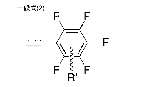
図8は、開始剤31および停止剤32の、電極20への表面修飾を説明するための図である。簡易のため、第1電極21および第2電極22の一対についてのみ説明する。上記一般式(1)にて示される開始剤31は、その一端のエチニル基と、第1電極21とが、表面修飾により接合される。停止剤32も、その一端のエチニル基と、第2電極22とが、表面修飾により接合される。なお、他の電極においても、表面修飾および架橋は同様に実行される。
次に、ステップ702として、分子鎖30の重合を開始する。すなわち、ステップ701にて電極20に接合された開始剤31を起端として、モノマを重合させていく。モノマとしては、下記一般式(3)で表されるものを用いる。この場合、分子鎖30は、下記一般式(4)で表される単位構造を持ち、パイ共役系高分子にて構成される。下記一般式において、「OR(RO)」は、アルキルオキシ基を示す。
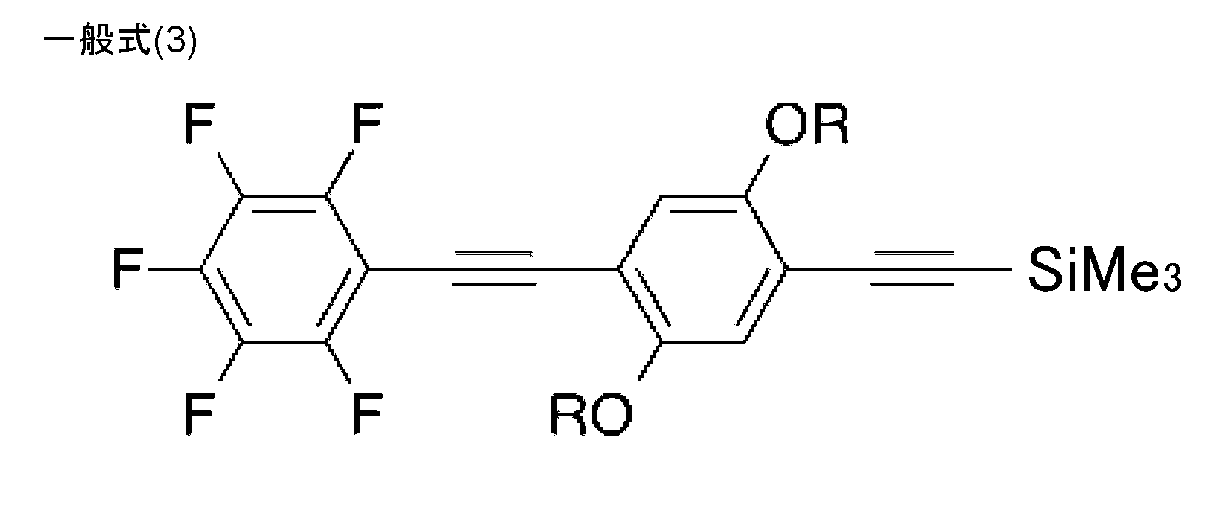

図9は、分子鎖30が重合されていく様子を説明するための図である。簡易のため、第1電極21および第2電極22の一対についてのみ説明する。重合が開始されると、上記一般式(4)のパイ共役系高分子が、開始剤31を起端に分子鎖30として生長していく。このように、分子鎖30の架橋が開始(即ち、重合が開始)される事象を、「リフトオフ」と称呼する。
以下、上記一般式(3)のモノマから、上記一般式(4)の単位構造を持つパイ共役系高分子が構成されるメカニズムについて、説明する。この重合には、触媒としてテトラブチルアンモニウムフルオリド(TBAF)を用いる。第1のモノマにおいては、TBAFをアニオンとして、その存在下においてトリメチルシリル基が脱離する。この脱離により、エチニル基がエチニルアニオンとなる。
一方、第2のモノマが有するペンタフルオロフェニル基は、第1のモノマにおけるエチニルアニオンと結合する。この結合は、ペンタフルオロフェニル基の4位炭素部位に形成される。この結合が形成される際、4位炭素部位に元々結合していたフッ素は脱離し、フッ化物アニオンが新たに生成することになる。新たに生成されたフッ化物アニオンにて、第2のモノマが有するトリメチルシリル基が脱離する。このプロセスが順次繰り返されることで重合していき、この結果、上記一般式(4)の単位構造で示されるパイ共役系高分子が構成される。
このように、TBAF触媒と、上記一般式(3)のモノマとにより、表面開始反応が生じる。これにより、上記リフトオフが達成される。すなわち、第1電極21に一端が接合された開始剤31にて、その他端のトリメチルシリル基が脱離し、開始剤31の他端側エチニル基と、モノマのペンタフルオロフェニル基の4位炭素とが結合する。そして順次モノマが付加されていくことで、上記一般式(4)の分子鎖30が生長していく。
次いで、ステップ703として、分子鎖30の重合を完了する。すなわち、ステップ701にて電極20に接合された停止剤32を終端として、重合を完了させる。
図10は、分子鎖30の重合が完了された状態を説明するための図である。簡易のため、第1電極21および第2電極22の一対についてのみ説明する。生長している分子鎖30の末端が停止剤32まで到達すると、この停止剤32への結合と同時に、分子鎖30の生長が停止する。このように、分子鎖30の架橋が完了(即ち、重合が完了)される事象を、「タッチダウン」と称呼する。
すなわち、生長する分子鎖30の末端(上記一般式(3)のモノマにおけるトリメチルシリル基の脱離後のエチニル基)と、停止剤32のペンタフルオロフェニル基の4位炭素とが結合する、いわゆる表面停止反応が生じる。これにより、上記タッチダウンが達成される。このように、上記リフトオフおよび上記タッチダウンによって、上記「重合開始・重合停止システム」が達成される。これによれば、重合時に副反応が生じ難いため、直鎖状の分子鎖の形成が可能となる。以上が、電極20間に分子鎖30を架橋するステップの説明である。
なお、本実施形態においては、開始剤31および停止剤32として、上記一般式(1)および上記一般式(2)にて表される自己組織化単分子膜を用いたが、これに代えて、例えば、下記一般式(5)および下記一般式(6)にて表されるものを用いてもよい。ここにおいて、「N」は窒素を表す。


また、分子鎖30の材料として、上記一般式(3)のモノマおよび上記一般式(4)の単位構造で表されるパイ共役系高分子を用いたが、これに代えて、他のモノマおよび単位構造が用いられてもよい。例えば、下記一般式(7)のモノマを用い、分子鎖30を、下記一般式(8)の単位構造で表されるものとしてもよい。ここにおいて、「O」、「S」「Bu」は、それぞれ酸素、硫黄、ブチル基を示す。


また、これらに代えて、例えば、下記一般式(9)のモノマを用い、分子鎖30を、下記一般式(10)の単位構造で表されるものとしてもよい。

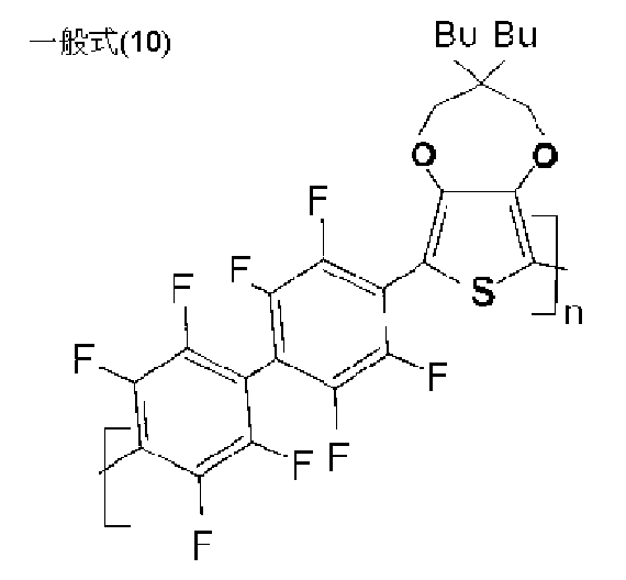
また、これらに代えて、例えば、下記一般式(11)のモノマを用い、分子鎖30を、下記一般式(12)の単位構造で表されるものとしてもよい。
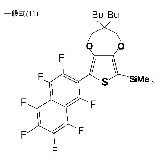

また、これらに代えて、例えば、下記一般式(13)のモノマを用い、分子鎖30を、下記一般式(14)の単位構造で表されるものとしてもよい。


また、これらに代えて、例えば、下記一般式(15)のモノマを用い、分子鎖30を、下記一般式(16)の単位構造で表されるものとしてもよい。


また、本実施形態においては、分子鎖30の架橋手法として「重合開始・重合停止システム」が用いられていたが、これに代えて、「重合開始・生長分子鎖結合停止システム」が用いられてもよい。この場合、例えば、先ず、架橋の起端としての開始剤31を第1,2電極21,22それぞれに接合した上で、これらの各開始剤31から対向するよう分子を生長させて、分子鎖30を形成してもよい。すなわち、第1,2電極21,22に接合された各開始剤31にて表面開始反応を生じさせ、各開始剤31から順次モノマを付加していくことで分子鎖30を各々生長させる。その後、各々生長する分子鎖30の末端同士で表面停止反応が生じることで、第1,2電極21,22間における分子鎖の架橋が達成される。
また、上述の重合に代えて、自己組織化に基づき上記架橋が達成されてもよい。この場合、例えば、架橋の起端としての開始剤31を、第1,2電極21,22それぞれに接合した上で、これらの各開始剤31から自己組織化させていくように、分子鎖30を形成してもよい。
<3.架橋評価ステップ>
次に、電極20に架橋された分子鎖30の架橋度合いを評価するステップについて、説明する。本ステップでは、上記リフトオフした量、および上記タッチダウンした量を、SERSを用いて定量する。この定量手法は、以下の知見に基づく。上述の<1.電極配設ステップ>にて得られる電極20は、金ナノ粒子として、超高密度に配置されている。このため、この電極20群に対する表面プラズモン増強電場により、大きなSERS利得が得られる。このSERS利得を取得するに際し、汎用的なラマン散乱装置が用いられ得る。他方、上述の増強電場は、表面から離間する距離に応じて、急激に減衰する傾向を有する。これらに基づき、上述の<2.分子鎖架橋ステップ>における、電極20への表面修飾、リフトオフ、およびタッチダウンに伴う、それぞれ電子状態の変化(すなわち、結合による分子振動の変化)を、簡易かつ感度良く追跡することができる。
次に、電極20に架橋された分子鎖30の架橋度合いを評価するステップについて、説明する。本ステップでは、上記リフトオフした量、および上記タッチダウンした量を、SERSを用いて定量する。この定量手法は、以下の知見に基づく。上述の<1.電極配設ステップ>にて得られる電極20は、金ナノ粒子として、超高密度に配置されている。このため、この電極20群に対する表面プラズモン増強電場により、大きなSERS利得が得られる。このSERS利得を取得するに際し、汎用的なラマン散乱装置が用いられ得る。他方、上述の増強電場は、表面から離間する距離に応じて、急激に減衰する傾向を有する。これらに基づき、上述の<2.分子鎖架橋ステップ>における、電極20への表面修飾、リフトオフ、およびタッチダウンに伴う、それぞれ電子状態の変化(すなわち、結合による分子振動の変化)を、簡易かつ感度良く追跡することができる。
図11は、SERSを用いた定量を説明するための、フローチャートである。このSERSを用いた定量は、上述の<1.電極配設ステップ>の後であって、<2.分子鎖架橋ステップ>の最中(即ち、「重合開始・重合停止システム」の最中)に、適宜導入される。このフローチャートにおける、上述した図7に示したステップと同じものにおいては、そのステップに対応する番号を付すことで説明に代える。
ステップ1101にて示すように、上述した「1.電極配設ステップ」にて得られた基板であって、表面修飾前のものに対し、ラマンスペクトルを取得する。具体的には、電極20が配設された基板10を溶媒に含浸させ、加え、開始剤31および停止剤32を含む溶液を滴下した状態にて、ラマン分光分析が実施される。すなわち、このラマン分光分析は、電極20への接合前(表面修飾前)の状態にて実施される。
図12は、取得されるラマンスペクトルの一部を説明するための図である。ステップ1101にて取得されるスペクトルは、実線で示されている。電極20近傍に開始剤31および停止剤32が遊離しており、上記スペクトルには、これらに由来するピークが含まれる。これらのピークにおける強度(高さ)は、開始剤31および停止剤32が、電極20に接合されていない状態に対応するものとなる。
本実施形態では、上記ピークとして、下記のとおり選択される。開始剤31に由来するピークとしては、開始剤31の末端におけるエチニル基炭素の三重結合に帰属するピークが選択される。停止剤32に由来するピークとしては、停止剤32の末端における、エチニル基炭素の三重結合に帰属するピークが選択される。選択される各ピークに対応する強度(高さ)を、「接合前開始剤ピーク強度Ii」および「接合前停止剤ピーク強度If」とそれぞれ称呼する。
次に、ステップ701にて示すように、上述した開始剤31および停止剤32にて電極20を表面修飾した後、ステップ1102に進み、表面修飾後の基板に対し、ラマンスペクトルを取得する。具体的には、上述したステップ1101における状態から所定時間経過後に、基板を溶媒にてリンスした状態にて、再度ラマン分光分析が実施される。すなわち、このラマン分光分析は、電極20への接合後(表面修飾後)の状態にて実施される。
図12の破線により、ステップ1102にて取得されるスペクトルが示されている。開始剤31および停止剤32が第1,第2電極21,22に接合されており、上記スペクトルには、これらに由来するピークが含まれる。これらのピークにおける強度(高さ)は、開始剤31および停止剤32が、電極20に接合されている状態に対応するものとなる。
接合後においては、上記溶媒に含有された開始剤31および停止剤32は、接合されたもの、および、接合されなかったものに大別される。上述のように選択されるピーク(実線ピークと同波数のピーク)の強度は、接合の量に応じた分だけ減少する。このときの破線ピークの強度が、上記接合後開始剤ピーク強度I’i(<Ii)および上記接合後停止剤ピーク強度I’f(<If)である。これらのピーク強度は、接合が達成されなかった開始剤31および停止剤32の量に等価なものとなる。他方、実線ピークからシフトした波数にて新たなピークが発現する。これらの新たなピークは、接合した量に応じた分だけ強度を有し、後述する「開始剤νC≡Cピーク」および「停止剤νC≡Cピーク」となる。これらの新たなピーク強度は、後述する「重合開始前開始剤ピーク強度Ipi」および「重合開始前停止剤ピーク強度Ipf」となる。
上述のように、接合前のスペクトル(実線、ステップ1101)と、接合後のスペクトル(破線、ステップ1102)との間における変化は、開始剤31および停止剤32において、それらが電極20に接合されることで、上記エチニル基の摂動態様が、接合前から変化することに基づく。なお、上記新たなピークの強度は、開始剤31および停止剤32に対して、理論的にはそれぞれIi-I’iおよびIf-I’fとなる。しかしながら、上記新たなピークの強度は、実際には、それらの値よりも小さいものとなる。
次に、ステップ1103に進み、開始剤31および停止剤32におけるピーク強度の減少率を設定する。具体的には、接合後開始剤ピーク強度I’iの、接合前開始剤ピーク強度Iiに対する減少率αを設定する。加え、接合後停止剤ピーク強度I’fの、接合前停止剤ピーク強度Ifに対する減少率βを設定する。減少率αおよび減少率βは、上記ステップ1101,1102にて取得されたIi,I’i,If,I’f、および、下記式(17)、式(18)に基づいて設定される。これらの式から解るように、減少率αは、「電極20近傍に遊離している開始剤31」の絶対量に対する、「電極20に接合した開始剤31」の絶対量の割合に相当する。減少率βは、「電極20近傍に遊離している停止剤31」の絶対量に対する、「電極20に接合した停止剤31」の絶対量の割合に相当する。
α=1-I’i/Ii ・・・(17)
β=1-I’f/If ・・・(18)
α=1-I’i/Ii ・・・(17)
β=1-I’f/If ・・・(18)
次に、ステップ1104に進み、重合開始する前における、開始剤31および停止剤32の表面修飾量を取得する。上記ステップ1103にて設定された減少率αと、上記溶液中における開始剤31の絶対量とに基づいて、「電極20に接合した開始剤31」の絶対量である開始剤表面修飾量ni0)を取得する。同様に、上記ステップ1103にて設定された減少率βと、上記溶液中における停止剤32の絶対量とに基づいて、「電極20に接合した停止剤32」の絶対量である停止剤表面修飾量nf0)を取得する。開始剤31および停止剤32の絶対量の検出には、種々化学分析が用いられ得、例えば、誘導結合プラズマ(Inductively Coupled Plasma、ICP)分析を用いると好適である。
他方、上記Ii,I’i,αと、開始剤表面修飾量ni0との関係を予め規定しておいてもよい。同様に、上記If,I’f,βと、停止剤表面修飾量nf0との関係を予め規定しておいてもよい。これらの関係は、下記のように検量線を取得することで規定され得る。例えば、ステップ701の直後に、電極基板にアルキルチオールをそれぞれ添加する。アルキルチオールは、開始剤31および停止剤32よりも電極20にて表面修飾され易い性質を有する。このため、アルキルチオールが添加されることで、電極基板において、電極20に接合されていた開始剤31および停止剤32が全て脱離し、代わりにアルキルチオールが電極20に接合されることになる。この脱離した開始剤31および停止剤32の量は、電極20に接合していた開始剤31の量(開始剤表面修飾量ni0)および停止剤32の量(停止剤表面修飾量nf0)と等価となる。従って、電極基板において、脱離した開始剤31および停止剤32の量をそれぞれ取得することで、開始剤表面修飾量ni0および停止剤表面修飾量nf0が、それぞれ取得される。取得されるni0およびnf0と、それらに対応する諸量(Ii,I’i,α、および、If,I’f,β)とを用い、検量線が取得される。
次に、ステップ1105に進み、ラマンスペクトル(開始前スペクトルに対応)を取得する。この取得に際しては、電極20に接合された開始剤31および停止剤32に対して、ラマン分光分析が実施される。すなわち、このラマン分光分析は、電極20への接合後であって重合が開始されていない状態にて実施される。
図13は、取得されるラマンスペクトルの一部を説明するための図である。ステップ1105にて取得されるスペクトルは、実線で示されている。このスペクトルには、開始剤31に由来するピークおよび停止剤32に由来するピークが含まれる。これらのピークにおける強度(高さ)は、重合開始前につき、電極20に開始剤31および停止剤32以外のものが接合されていない状態に対応するものとなる。
本実施形態では、上記ピークとして、下記のとおり選択される。開始剤31に由来するピークとしては、開始剤31の第1電極21と接合している側における、エチニル基炭素の三重結合に帰属するピーク(開始剤νC≡Cピーク)が選択される。停止剤32に由来するピークとしては、停止剤32の第2電極22と接合している側における、エチニル基炭素の三重結合に帰属するピーク(停止剤νC≡Cピーク)が選択される。選択される各ピークに対応する強度(高さ)を、「重合開始前開始剤ピーク強度Ipi」および「重合開始前停止剤ピーク強度Ipf」とそれぞれ称呼する。
次に、ステップ702,703に順に進み、分子鎖30の重合を開始した後に、分子鎖30の重合を完了する。
次いで、ステップ1106に進み、ラマンスペクトル(開始後スペクトルに対応)を取得する。この取得に際しても、電極20に接合された開始剤31および停止剤32に対して、ラマン分光分析が実施される。すなわち、このラマン分光分析は、重合が開始された後であって重合が完了した状態にて実施される。
図13によれば、ステップ1103にて取得されるスペクトルは、破線で示されている。このスペクトルにも、開始剤31に由来するピークおよび停止剤32に由来するピークが含まれる。これらのピークにおける強度(高さ)は、重合開始後であって重合完了後につき、開始剤31および停止剤32に、上記一般式(1)のモノマが接合した状態に対応するものとなる。
本実施形態では、このスペクトルにおいて、上記開始剤νC≡Cピークおよび上記停止剤νC≡Cピークが選択される。選択される各ピークに対応する強度(高さ)を、「重合開始後開始剤ピーク強度I’pi」および「重合開始後停止剤ピーク強度I’pf」とそれぞれ称呼する。
重合開始後においては、電極20に接合された全開始剤31は、リフトオフが達成されたもの、および、リフトオフが達成されなかったものに大別される。開始剤νC≡Cピーク(実線ピークと同波数のピーク)の強度は、リフトオフの量に応じた分だけ減少する。このときの破線ピークの強度が、上記重合開始後開始剤ピーク強度I’pi(<Ipi)である。このピーク強度は、リフトオフが達成されなかった開始剤31の量に等価なものとなる。他方、実線ピークからシフトした波数にて新たなピークが発現する。この新たなピークは、リフトオフの量に応じた分だけ強度を有する。
重合完了後においては、電極20に接合された全停止剤32は、タッチダウンが達成されたもの、および、タッチダウンが達成されなかったものに大別される。停止剤νC≡Cピーク(実線ピークと同波数のピーク)の強度は、タッチダウンの量に応じた分だけ減少する。このときの破線ピークの強度が、上記重合開始後停止剤ピーク強度I’pf(<Ipf)である。このピーク強度は、タッチダウンが達成されなかった停止剤32の量に等価なものとなる。他方、実線ピークからシフトした波数にて新たなピークが発現する。この新たなピークは、タッチダウンの量に応じた分だけ強度を有する。
上述のように、重合開始前のスペクトル(実線、ステップ1105)と、重合完了後のスペクトル(破線、ステップ1106)との間における変化は、開始剤31および停止剤32において、上記一般式(1)のモノマが付加されることで、上記エチニル基の摂動態様が、付加される前から変化することに基づく。なお、上記新たなピークの強度は、開始剤31および停止剤32に対して、理論的にはそれぞれIpi-I’piおよびIpf-I’pfとなる。しかしながら、上記新たなピークの強度は、実際には、それらの値よりも小さいものとなる。
次に、ステップ1107に進み、開始剤31および停止剤32におけるピーク強度の減少率を設定する。具体的には、重合開始後開始剤ピーク強度I’piの、重合開始前開始剤ピーク強度Ipiに対する減少率γを設定する。加え、重合開始後停止剤ピーク強度I’pfの、重合開始前停止剤ピーク強度Ipfに対する減少率δを設定する。減少率γおよび減少率δは、上記ステップ1105,1106にて取得されたIpi,I’pi,Ipf,I’pf、および、下記式(19)、式(20)に基づいて設定される。これらの式から解るように、減少率γは、「電極20に接合された全開始剤31」の絶対量に対する、「実際に重合開始した開始剤31」の絶対量の割合に相当する。減少率δは、「電極20に接合された全停止剤32」の絶対量に対する、「実際に重合停止させた停止剤32」の絶対量の割合に相当する。
γ=1-I’pi/Ipi ・・・(19)
δ=1-I’pf/Ipf ・・・(20)
γ=1-I’pi/Ipi ・・・(19)
δ=1-I’pf/Ipf ・・・(20)
次いで、ステップ1108に進み、実際に開始剤31からリフトオフが達成された開始剤31の量を取得する。加え、実際に停止剤32にタッチダウンが達成された停止剤32の量を取得する。これらの量を、「リフトオフ量ni1」および「タッチダウン量nf1」とそれぞれ称呼する(リフトオフ量および/またはタッチダウン量が、隣り合う電極間における架橋数に相当する)。リフトオフ量ni1およびタッチダウン量nf1は、上記ステップ1104にて取得されたni0,nf0、上記ステップ1107にて設定されたγ,δ、および、下記式(20)、式(21)に基づいて取得される。
ni1=γ・ni0 ・・・(20)
nf1=δ・nf0 ・・・(21)
ni1=γ・ni0 ・・・(20)
nf1=δ・nf0 ・・・(21)
このように、SERSを用いることで、電極20への表面修飾、リフトオフ、およびタッチダウンに伴う、それぞれ電子状態の変化(すなわち、結合による分子振動の変化)を、簡易かつ感度良く追跡することができる。この結果、リフトオフ量ni1およびタッチダウン量nf1が、それぞれ精度良く取得され得、電極20への架橋数を評価することができる。以上が、電極20に架橋された分子鎖30の架橋度合いを評価するステップの説明である。
なお、本実施形態においては、開始剤31の第1電極21側のC≡Cに帰属するピークに基づいて、リフトオフ量ni1が取得されるが、これに加え、SiMe3側のC≡Cに帰属するピークにも基づいてもよい。また、SiMe3側のC≡Cに帰属するピークのみに基づいて、リフトオフ量ni1が取得されてもよい。
また、リフトオフ量ni1およびタッチダウン量nf1の取得のためのピークとして、開始剤31のC≡Cに帰属するピークおよび停止剤32のC≡Cに帰属するピークが選択されている。これに加え、開始剤31(上記一般式(1))のRおよび停止剤32(上記一般式(2))のR’にそれぞれ対応する官能基帰属のピークも選択してもよい。これにより、リフトオフ量ni1およびタッチダウン量nf1の信頼性が向上され得る。
また、本実施形態においては、分子鎖30の架橋度合いの評価のために、リフトオフ量ni1およびタッチダウン量nf1の両方が取得されるが、これに代えて、リフトオフ量ni1およびタッチダウン量nf1のうち何れか一方のみが取得されるようにしてもよい。
また、本実施形態においては、スペクトルの取得に際し、ラマン分光分析を用いたが、これに代えて、例えばX線光電子分光分析を用いてもよい。
<4.抵抗値取得ステップ>
次に、隣り合う電極20の間における抵抗値を取得するステップについて、説明する。本実施形態にかかる分子配線基板においては、電極20の数が夥しい数であり、その間隔はナノメートルレベルである。したがって、この基板における伝導特性の評価は、上述した「一括評価」が利用できる。これにより、分子鎖30と電極20との接合における不均一性、分子鎖30の架橋数の分散が、評価に繰り込まれ得る。
次に、隣り合う電極20の間における抵抗値を取得するステップについて、説明する。本実施形態にかかる分子配線基板においては、電極20の数が夥しい数であり、その間隔はナノメートルレベルである。したがって、この基板における伝導特性の評価は、上述した「一括評価」が利用できる。これにより、分子鎖30と電極20との接合における不均一性、分子鎖30の架橋数の分散が、評価に繰り込まれ得る。
図14は、分子鎖30を架橋した電極20群を示す模式図である。この模式図は、上述した図1に対応するものであり、電極20の配設および分子鎖30の架橋が、理想的に実施された状態のものを示す。理想的な状態とは、各電極20のドットはそれぞれ同一の大きさであり、等間隔に配設された状態である。それに加え、各分子鎖30は、各電極20間にそれぞれ1本ずつ、直線的に同じ長さで架橋される。これにより、理想的には、何れの場所においても、完全な三角格子が形成される。なお、実際の電極20および分子鎖30は、図1に示すように、必ずしも完全な三角格子が形成されるわけではない。このため、分子鎖30と電極20との接合における不均一性や、分子鎖30の架橋数の分散が生じる。
例えば、所定の電極20間に、電気・熱等のエネルギを印加した場合、この無数の三角格子を介して、伝導経路が形成されることになる。この伝導経路は、平面的に編み目状に広がっている。このため、一般に、合成抵抗(総括の伝導率)の決定は、その広がりに応じてより複雑となる。この複雑さを緩和する観点から、本実施形態では、伝導経路の規定に関し、Δ→Y変換およびY→Δ変換を利用する。
図15は、本実施形態にかかる分子配線基板における、Δ→Y変換およびY→Δ変換について説明するための図である。1つの最小単位の三角格子に着目する。この三角格子を、Δ→Y変換におけるΔ要素と見なすことができる。Δ要素において、電極a、b、c間を架橋する分子鎖30の抵抗(1つの電極間における抵抗)を、それぞれrとする。すなわち、「r」は、Δ要素における平均抵抗を示すことになる。この値は、後述する抵抗値R1に相当する。
このΔ要素について、Δ→Y変換を実施すると、Δ要素の中央を起点とし、電極a、b、cとそれぞれ接続される、3つの仮想経路が発現する。電極a、b、cと、この3つの仮想経路とで、Δ→Y変換におけるY要素が構成される。Y要素において、上記仮想経路に対応する抵抗を、それぞれRとする。ここにおいて、Δ要素およびY要素は、等価回路の関係にあるので、rとRとの間には、R=r/3の関係が成立する。
次に、基板における1つの三角格子であって、Δ要素の一辺が3つの電極20分に相当する格子に着目する。頂点をなす電極a、b、cに加え、各辺の中間に電極ab、bc、caが位置する。これら中間の電極ab、bc、ca同士も、相互に伝導する経路が構成される。ここにおいて、3つの電極a、ab、ca、3つの電極b、ab、bc、および3つの電極c、ca、bcにて構成される各Δ要素に対して、上述のΔ→Y変換を実施する。これにより、各Y要素において、(1/3)rの抵抗値が得られる。ここにおいて、上記各Δ要素におけるそれぞれの中央の3点を接続すると、等価回路として、新たなΔ要素が発現する。このΔ要素の一辺は、(2/3)rとなる。
更に、上記新たに発現したΔ要素について、Δ→Y変換を実施する。このΔ要素の中央を起点とし、上述と同様の3つの仮想経路(r、Rの関係から、抵抗は(2/9)r)が発現する。この3つの仮想経路は、それぞれ、電極a、b、cまで延長されることになる。したがって、このΔ要素の中央を起点とし、電極a、b、cまで接続された、新たなY要素が発現する。このY要素における1つの仮想経路の抵抗は、(1/3)r+(2/9)r=(5/9)rとなる。
更に、上記新たに発現したY要素について、Y→Δ変換を実施する。すなわち、電極a、b、cを頂点とするΔ要素に着目すると、その一辺の抵抗値は、r、Rの関係から(5/3)rとなる。この値は、後述する抵抗値R2に相当する。
図16は、本実施形態にかかる分子配線基板における、Δ要素における一辺の抵抗値RXを説明するための図である。上述では、N1=1およびN2=2の場合における、抵抗値R1およびR2が算出された。これは、Δ→Y変換およびY→Δ変換に基づいており、N1、N2における各抵抗値R1、R2ので、漸化関係が成立する。また、RXは、NX=20、21、22・・・2X-1の等比数列にそれぞれ対応する。したがって、一般化すると、階数X=X(自然数)である場合、下記漸化式(22)が成立する。上述のとおり、このような三角格子の一辺における伝導経路の抵抗値を決定する際、本来ならば複雑化する。しかしながら、本実施形態にかかる分子配線基板においては、下記式(22)を利用することで、複雑さが緩和され得る。
RX=(5/3)(X-1)r ・・・(22)
RX=(5/3)(X-1)r ・・・(22)
図17は、本実施形態にかかる分子配線基板において、電極20間における抵抗値の一括評価について、説明するための図である。基板10の端部に配設された電極20であって、相互に十分に離間した4つ電極A、B、C、Dに着目する。これらの電極20の間隔は、隣り合う電極20の間隔に比して、十分に大きい。この4つの電極A、B、C、Dにおいては、3つの電極A、B、C、および3つの電極A、B、Dにて、2つの三角格子(すなわちΔ要素)が形成される。電極A、Bを接続する伝導経路は、2つの三角格子の一辺を共通するものとする。
ここにおいて、電極A,Bを接続する伝導経路の途中において、プローブを挿入する場合を考える。このプローブは、各先端P1、P2で相互離間した2つの針状プローブである。この各先端P1、P2を電極20に接続させることで、各先端の間隔に対応する抵抗値(後述のグロス抵抗GR)を検出するようになっている。このプローブ先端P1、P2(に対応する電極20)の間隔Dは、隣り合う電極における間隔よりも十分に大きく、且つ、電極A‐B間、B‐C間、C-A間、B-D間、D-A間の経路に対応する間隔よりも十分に小さい。
図18は、2つの針状プローブPを用いた抵抗値の検出について説明するための図である。2つの針状プローブPは、それらの先端P1,P2が所定の間隔をもつよう配置される。この所定の間隔を間隔D(検出間隔Dに対応)とする。針状プローブPに向けて、電流が出力されるようになっている。この電流は、所定の範囲にて可変に制御される。従って、上述のとおりプローブ先端P1、P2を電極20に接続させることで、P1、P2を介して、制御された電流が導通する。この電流値と、対応する電圧値との関係を取得することで、I-V特性が得られる。I-V特性の勾配に基づき、抵抗値(グロス抵抗GR)が決定される。このように、グロス抵抗GRは、所謂2端子法にて検出される。なお、本実施形態においては、抵抗値の検出に際し2端子法を用いているが、これに代えて、例えば4端子法を用いてもよい。
図17に示すように、この場合、プローブの各先端P1、P2を検出点として、等価回路が構成される。この等価回路は、P1‐A間、P2‐B間、P1‐P2間、A‐C間、C‐B間、B‐D間、およびD‐A間における7種類の経路が規定される。各経路に対応するΔ要素の階数をP,Q,L,Mとすると、各経路におけるNXおよび抵抗値RXは、上記式(22)に基づいて下記のとおりそれぞれ表される。
P1‐A間 :RP=(5/3)(P-1)r、NP=2P-1
P2‐B間 :RQ=(5/3)(Q-1)r、NQ=2Q-1
P1‐P2間 :RL=(5/3)(L-1)r、NL=2L-1
A‐C(C‐B、B‐D、D‐A)間
:RM=(5/3)(M-1)r、NM=2M-1
P1‐A間 :RP=(5/3)(P-1)r、NP=2P-1
P2‐B間 :RQ=(5/3)(Q-1)r、NQ=2Q-1
P1‐P2間 :RL=(5/3)(L-1)r、NL=2L-1
A‐C(C‐B、B‐D、D‐A)間
:RM=(5/3)(M-1)r、NM=2M-1
プローブの各先端P1、P2にて検出されるグロス抵抗をGRとすると、上記RP、RQ、RL、RMを用い、グロス抵抗GRは、等価回路から下記式(23)で表される。これは、A‐C間とC‐B間の合成抵抗2RMと、B‐D間とD‐A間の合成抵抗2RMとを並列させた場合における、A‐B間の合成抵抗がRM(=1/((1/2RM)+(1/2RM))、破線部を参照)であることに基づく。更に、等価回路から、上記抵抗値RP、RQ、RL、RMは、下記式(24)で表される関係で規定される。
1/GR=1/RL+1/(RP+RQ+RM) ・・・(23)
RM=RP+RQ+RL ・・・(24)
1/GR=1/RL+1/(RP+RQ+RM) ・・・(23)
RM=RP+RQ+RL ・・・(24)
上記式(23)は、上記式(24)を用いることで、下記式(26)に変形され得る。ここにおいて、係数Kは、下記式(27)で示される値である。図19に示すように、係数Kは、係数Kと比率RL/RMとの関係を規定したグラフと、抵抗RL,RMとに基づいて決定され得る。例えば、プローブ先端P1、P2の間隔Dが十分に小さく、L<<MかつRL<<RMである場合、Kは限りなく「1」に近づく。この場合は、K=1と近似してもよい。
GR=(K)RL=(K)(5/3)(L-1)r ・・・(26)
K=1-(1/2)(RL/RM)=1-(1/2)(3/5)(M-L) ・・・(27)
GR=(K)RL=(K)(5/3)(L-1)r ・・・(26)
K=1-(1/2)(RL/RM)=1-(1/2)(3/5)(M-L) ・・・(27)
他方、P1‐P2間の経路において、隣り合う電極20における間隔をdとすると、間隔dと、間隔Dとの間には、下記式(28)で表される関係が規定される。更に、基板10のサイズをZ0とすると、間隔dと、サイズZ0との間には、下記式(29)で表される関係が規定される。これら式(28)および式(29)を用い、上記式(27)よりL,Mを消去することで、下記式(30)が得られる。図20に示すように、係数Kは、係数Kと比率Z0/Dとの関係を規定したグラフと、間隔Dと、サイズZ0とに基づいて決定することもできる。例えば、Z0/D=3、10、20である場合、K=0.78、0.92、0.96となる。
D=NLd=2(L-1)d ・・・(28)
Z0=NMd=2(M-1)d ・・・(29)

D=NLd=2(L-1)d ・・・(28)
Z0=NMd=2(M-1)d ・・・(29)
上記式(26)を対数変換し(logGR=(L-1)log(5/3)+log(Kr))、上記式(28)を対数変換し(logD=(L-1)log2+log(d))、これらを用いて上記式(26)中の(L-1)を消去することで、下記式(31)が得られる。ここにおいて、係数Jは、下記式(32)で示される値である。
logGR=(J)log(D/d)+log(Kr) ・・・(31)
J=log(5/3)/log2=0.7369655941 ・・・(32)
logGR=(J)log(D/d)+log(Kr) ・・・(31)
J=log(5/3)/log2=0.7369655941 ・・・(32)
上記式(31)と、プローブにて検出されるグロス抵抗値GRと、プローブ先端P1、P2の間隔Dと、隣り合う電極20の間隔dとに基づけば、容易に隣り合う電極20における抵抗値rを決定することができる。より具体的には、例えば、間隔Dを複数異ならせながら、対応するグロス抵抗値GRをそれぞれ取得する。そして、縦軸をlogGR、横軸をlog(D/d)として、logGRおよびlog(D/d)との関係を規定するグラフを描画する。このグラフは、上記式(31)より、一次関数の直線となる。したがって、描画したグラフにおいて、log(D/d)=0に対応するlogGR(すなわち、直線の切片)が、log(Kr)と同値となる。このことに基づいて、抵抗値rが決定され得る。
このようにして決定される抵抗値rは、隣り合う電極間における平均抵抗値であって、分子鎖30と電極20との接合における不均一性、分子鎖30の架橋数の分散が繰り込まれたものとなり得る。従って、隣り合う電極20間に架橋された分子鎖30において、伝導特性を再現性良く決定され得る。このことは、隣り合う電極20における実効的な抵抗値が得られることと、等価である。
これに加え、上記<3.架橋評価ステップ>にて決定された分子鎖30のリフトオフ量およびタッチダウン量(分子鎖30の架橋数)も用いることで、単位分子鎖30あたりの伝導性も評価することができる。隣り合う電極間における分子鎖1本あたりの抵抗値および電気伝導率を、singlerおよびsinglesとすると、これらは下記式(33)および下記式(34)と、上記式(31)より決定された抵抗値rと、上記式(21)より決定されたタッチダウン量nf1とに基づいて、それぞれ決定され得る。なお、タッチダウン量nf1に代えて、リフトオフ量ni1を用いてもよい(上記式(20)を参照)。このように、上述の4つのステップを経る本実施形態の分子配線基板によれば、分子の伝導性の評価に対し、十分な信頼性を得ることができる。
singler=r/nf1 ・・・(33)
singles=nf1/r(=1/singler) ・・・(34)
singler=r/nf1 ・・・(33)
singles=nf1/r(=1/singler) ・・・(34)
なお、本実施形態における抵抗値rの決定は、電極20で構成される三角格子において、各辺に対応する抵抗値rがそれぞれ同一であるものとしてなされている。これに代えて、例えば、Δ要素の各辺に対応する抵抗値が、それぞれ異なっていてもよい。この場合においても、抵抗値のΔ→Y変換およびY→Δ変換に基づいて伝導経路が規定され得る。以下、本実施形態の変形例として、Δ要素の各辺に対応する抵抗値がそれぞれ異なっている場合における、Δ→Y変換およびY→Δ変換について説明する。
図21は、本実施形態の変形例にかかる分子配線基板における、Δ→Y変換およびY→Δ変換について説明するための図である。この図21は、上述した図15に対応するものであり、共通する部位・計算については図15のものを援用することで、説明を省略する。基板10における1つの三角格子であって、最小単位の三角格子に着目する。このΔ要素において、電極a‐b、b‐c、c‐a間を架橋する分子鎖の抵抗を、それぞれr1、r2、r3とする。このΔ要素についてΔ→Y変換を実施すると、Y要素が得られる。このY要素における仮想経路に対応する抵抗を、それぞれR1、R2、R3とする。ここにおいて、r1、r2、r3と、R1、R2、R3との間には、下記の関係が成立する。
R1=r3r1/(r1+r2+r3)
R2=r1r2/(r1+r2+r3)
R3=r2r3/(r1+r2+r3)
R1=r3r1/(r1+r2+r3)
R2=r1r2/(r1+r2+r3)
R3=r2r3/(r1+r2+r3)
次に、基板における1つの三角格子であって、X=2に対応する格子に着目する。電極a‐ab、ab‐ca、ca‐a間を架橋する分子鎖の抵抗を、それぞれrA1、rA2、rA3とする(Δ要素A)。電極ab‐b、b‐bc、bc‐ab間を架橋する分子鎖の抵抗を、それぞれrB1、rB2、rB3とする(Δ要素B)。電極ca-bc、bc‐c、c‐ca間を架橋する分子鎖の抵抗を、それぞれrC1、rC2、rC3とする(Δ要素C)。Δ要素A、Δ要素B、およびΔ要素Cに対して、上述のΔ→Y変換を実施すると、それぞれに対応するY要素A、Y要素B、およびY要素Cが得られる。Y要素Aにおける仮想経路に対応する抵抗を、それぞれrAR1、rAR2、rAR3とする。Y要素Bにおける仮想経路に対応する抵抗を、それぞれrBR1、rBR2、rBR3とする。Y要素Cにおける仮想経路に対応する抵抗を、それぞれrCR1、rCR2、rCR3とする。これら3つの各Y要素において、上記r1、r2、r3と、R1、R2、R3との間の関係に基づき、下記の関係が成立する。
Y要素A(Δ要素A):
rAR1=(rA3)(rA1)/(rA1+rA2+rA3)
rAR2=(rA1)(rA2)/(rA1+rA2+rA3)
rAR3=(rA2)(rA3)/(rA1+rA2+rA3)
Y要素B(Δ要素B):
rBR1=(rB3)(rB1)/(rB1+rB2+rB3)
rBR2=(rB1)(rB2)/(rB1+rB2+rB3)
rBR3=(rB2)(rB3)/(rB1+rB2+rB3)
Y要素C(Δ要素C):
rCR1=(rC3)(rC1)/(rC1+rC2+rC3)
rCR2=(rC1)(rC2)/(rC1+rC2+rC3)
rCR3=(rC2)(rC3)/(rC1+rC2+rC3)
Y要素A(Δ要素A):
rAR1=(rA3)(rA1)/(rA1+rA2+rA3)
rAR2=(rA1)(rA2)/(rA1+rA2+rA3)
rAR3=(rA2)(rA3)/(rA1+rA2+rA3)
Y要素B(Δ要素B):
rBR1=(rB3)(rB1)/(rB1+rB2+rB3)
rBR2=(rB1)(rB2)/(rB1+rB2+rB3)
rBR3=(rB2)(rB3)/(rB1+rB2+rB3)
Y要素C(Δ要素C):
rCR1=(rC3)(rC1)/(rC1+rC2+rC3)
rCR2=(rC1)(rC2)/(rC1+rC2+rC3)
rCR3=(rC2)(rC3)/(rC1+rC2+rC3)
ここにおいて、上記各Δ要素におけるそれぞれの中央の3点を接続すると、等価回路として、新たなΔ要素Gが発現する。このΔ要素Gの各辺に対応する抵抗を、rG1、rG2、rG3とすると、それぞれ下記のとおり表される。
rG1=rAR2+rBR1
rG2=rBR3+rCR2
rG3=rCR1+rAR3
rG1=rAR2+rBR1
rG2=rBR3+rCR2
rG3=rCR1+rAR3
更に、上記Δ要素Gについて、Δ→Y変換を実施する。変換されたY要素における各仮想経路に対応する抵抗を、rGR1、rGR2、rGR3とする。このY要素において、上記r1、r2、r3と、R1、R2、R3との間の関係に基づき、下記の関係が成立する。この変換により、中央を起点とし、電極a、b、cまで接続された新たなY要素が発現する。このY要素における各仮想経路の抵抗を、rH1、rH2、rH3とすると、それぞれ下記のとおり表される。
rGR1=(rG3)(rG1)/(rG1+rG2+rG3)
rGR2=(rG1)(rG2)/(rG1+rG2+rG3)
rGR3=(rG2)(rG3)/(rG1+rG2+rG3)
rH1 =rAR1+rGR1
rH2 =rBR2+rGR2
rH3 =rCR3+rGR3
rGR1=(rG3)(rG1)/(rG1+rG2+rG3)
rGR2=(rG1)(rG2)/(rG1+rG2+rG3)
rGR3=(rG2)(rG3)/(rG1+rG2+rG3)
rH1 =rAR1+rGR1
rH2 =rBR2+rGR2
rH3 =rCR3+rGR3
更に、上記新たに発現したY要素について、Y→Δ変換を実施する。すなわち、電極a、b、cを頂点とするΔ要素に着目し、各辺の抵抗を、rh1、rh2、rh3とすると、それぞれ下記のとおり表される。
rh1=[(rH1)(rH2)+(rH2)(rH3)+(rH3)(rH1)]/rH3
rh2=[(rH1)(rH2)+(rH2)(rH3)+(rH3)(rH1)]/rH1
rh3=[(rH1)(rH2)+(rH2)(rH3)+(rH3)(rH1)]/rH2
rh1=[(rH1)(rH2)+(rH2)(rH3)+(rH3)(rH1)]/rH3
rh2=[(rH1)(rH2)+(rH2)(rH3)+(rH3)(rH1)]/rH1
rh3=[(rH1)(rH2)+(rH2)(rH3)+(rH3)(rH1)]/rH2
下記式(35)は、上記抵抗値のrh1についての展開式を示す図である。すなわち、抵抗値rh1は、図21のΔ要素における各抵抗値rA1、rA2、rA3、rB1、rB2、rB3、rC1、rC2、rC3、および上述した各関係式を用いて、本展開式のとおり示される。なお、rh2、rh3についても同様に展開され得る。この展開式と、上述した漸化関係とに基づけば、上記実施形態と同様の伝導性の一括評価が可能となる。このように、Δ要素の各辺に対応する抵抗値がそれぞれ異なっている場合においても、伝導性の一括評価が達成され得る。
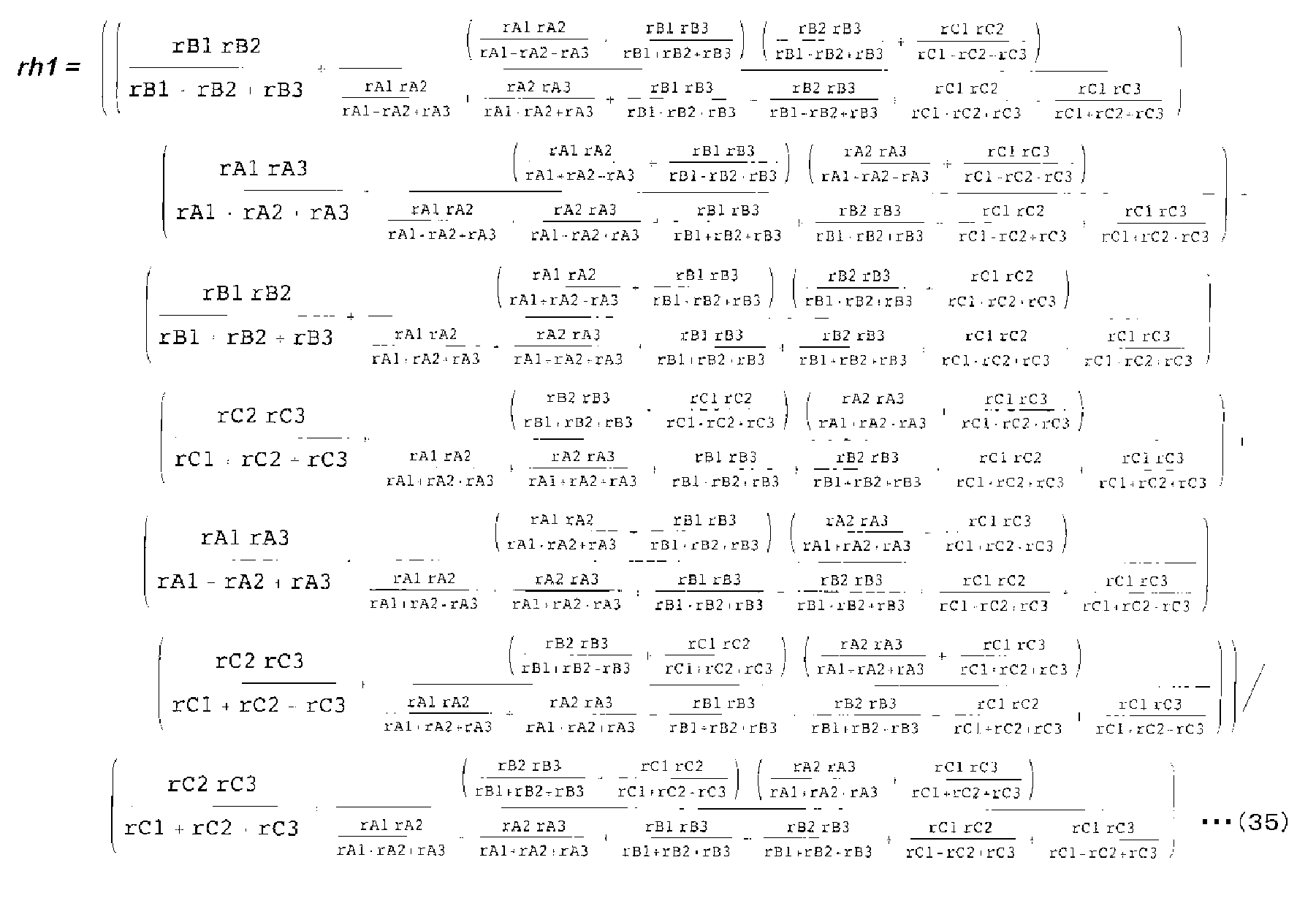
図22は、上述したΔ→Y変換およびY→Δ変換において、合成抵抗に対する、Δ要素の各抵抗値におけるばらつきの影響を説明するための図である。本例では、Δ要素の各辺に対応する抵抗値がそれぞれ異なっている場合を想定し、数値計算により、合成抵抗の分散発展をシミュレートした。上述した漸化関係における階数X=1,・・・,5における合成抵抗Rxに対し、確率密度関数を計算した。なお、X=5における抵抗R5は、X=1のΔ要素に対し、2(5-1)=16倍のスケールをもつ相似なΔ要素における合成抵抗に相当する。これらの合成抵抗Rxは、Δ要素の抵抗値におけるばらつきが、正規分布に従うものと仮定して計算される。この正規分布においては、上記抵抗値の平均、標準偏差、および乱数発生個数を、それぞれ10、5、および24,300に設定した。
合成抵抗の確率密度関数によれば、階数Xが1から5にインクリメントされるに応じて、抵抗値の平均は、略5/3倍ずつ増大していく。これは、等価六方格子の項比が5/3であることに対応する。他方、標準偏差も上記インクリメントに応じ増大していくものの、相対標準偏差(RSD=標準偏差/平均)は、略0.8倍ずつ減少していく。即ち、X=1ではRSD=0.48であるが、X=5においてはRSD=0.19となった。
合成抵抗を計算するにあたり、実際のスケールに相当する条件を設定した。その条件として、間隔dおよび間隔Dを、それぞれ10nmおよび1.0mmに設定した。この条件の場合、上述した(28)式によれば、L=17.6となり、対応する相対標準偏差は、略2.0%となった。これは、簡易なΔ→Y変換およびY→Δ変換の繰り返しのみで、発生させた乱数の分散が、略2.0%まで激減することを意味する。即ち、プローブ間隔の距離を、D=1.0mmに対応させれば、抵抗値の誤差を略2.0%に収斂させることができる(この計算結果は、電極への分子鎖の結線が、部分的になされていなくてもよいことを、示唆している。)。このように、Δ要素の各辺に対応する抵抗値がそれぞれ異なっており、ばらつきがある場合であっても、分子の伝導性の評価に対し、十分な信頼性を得ることができる。
また、上記実施形態においては、上述の漸化関係における階数Xに自然数を適用していたが、これにかえて、階数Xに実数を適用してもよい。
<抵抗値rの評価についての検証>
次に、本実施形態の分子配線基板における抵抗値rの評価についての、検証の例を説明する。具体的には、上記式(33)と、上記間隔dと、上記間隔Dと、グロス抵抗GRとを用い、実際に決定される抵抗値rが、妥当であることを検証した。すなわち、上述したプロセスに則すれば、十分に信頼性ある抵抗値rを取得できる旨を説明する。なお、この検証例においては、基板における電極の配置が六方格子とされ、それらが細線で接続されていれば十分である。従って、スケールの大小は無関係である。
次に、本実施形態の分子配線基板における抵抗値rの評価についての、検証の例を説明する。具体的には、上記式(33)と、上記間隔dと、上記間隔Dと、グロス抵抗GRとを用い、実際に決定される抵抗値rが、妥当であることを検証した。すなわち、上述したプロセスに則すれば、十分に信頼性ある抵抗値rを取得できる旨を説明する。なお、この検証例においては、基板における電極の配置が六方格子とされ、それらが細線で接続されていれば十分である。従って、スケールの大小は無関係である。
図23は、この検証に用いた模擬的な分子配線基板を示す図である。模擬的な分子配線基板は、模擬基板100(本実施形態の基板10に対応)と、模擬電極200(本実施形態の電極20に対応)と、模擬分子鎖300(本実施形態の分子鎖30に対応)とを備える。模擬基板100上には、無数の模擬電極200を、それぞれ三角格子状となるよう配設した。各模擬電極は、それぞれ円形のドットで構成される。隣り合う模擬電極200における各中心間距離(本実施形態の間隔dに対応)は、200μmであり、隣り合う模擬電極200間を、模擬分子鎖300にてそれぞれ架橋した。模擬分子鎖300の断面は、長方形状を呈している。模擬基板100は、14mm角の平板であり、非ドープシリコンウェハ(3000 Ωcm)で構成されている。模擬電極200および模擬分子鎖300は、それぞれ銀を主材として構成されている。なお、模擬基板100上には、所定の模擬電極200と導通する複数の測定点400,410,420,430が備えられている。これらの測定点は、後述の針状プローブの先端が接触可能となっている。
上記構成の模擬的な分子配線基板は、下記のとおり作成した。模擬基板100上に、模擬電極200および模擬分子鎖300を、上記構成となるように超微細インクジェット装置(株式会社SIJテクノロジ製)にて描画した。インクジェット原料には、銀ナノ粒子を分散させたインク(ハリマ化成株式会社製)を用いた。描画条件としては、On:1mm/s、Off:4mm/sとし、2回描画した。描画後の基板を全体的に焼成し(220℃,1hr、真空中)、インク内の分散剤を分解・脱離させた。
上述のように作成した模擬的な分子配線基板において、隣り合う模擬電極200間における模擬分子鎖300の抵抗値r’(本実施形態の抵抗値rに対応)を決定した。この抵抗値r’を、隣り合う模擬電極200間における距離(200μm)で除すことで、単位長さあたりの抵抗値ρを算出した。
上記抵抗値r’を、下記のとおり決定した。2つの針状プローブを5通りに配置させて(第1配置、第2配置、第3配置、第4配置、および第5配置)、その配置に応じた抵抗値r’を決定した。複数の測定点400,410,420,430から任意の2つをピックアップし、針状プローブをそれらに接触させるようにして、プローブ間隔を異ならせた。第1~第5配置におけるプローブ間隔(本実施形態の間隔Dに対応)は、それぞれ2336 μm,2312 μm,3991 μm,3790 μm,1318 μmの5通りである。これらのプローブの配置状態にて、プローブに向けて電流をそれぞれ出力した。出力電流を、-100 mAから100 mAまで変化させた。これら変化させた各電流に対応する電圧をそれぞれ測定した。この測定を、1通りのプローブ配置毎に計5回実施することで、I-V特性を取得した。
図24は、プローブ配置が第1配置(プローブ間隔:2336 μm)である場合における、上記I-V特性に相当する電流と電圧との関係を示すグラフである。計5回の測定においても、各直線は略一致し、良好な再現性を有していた。電流および電圧は、互いに一次の比例関係を有する。従って、直線の勾配が、グロス抵抗GRに相当する。本知見に基づき、図24のグラフより、第1配置に対応するグロス抵抗GR=1.98×101±0.01×101 Ωと決定した。同様に、第2配置、第3配置、第4配置、および第5配置に対応するグロス抵抗GRを、1.97×101±0.00×101 Ω,4.09×101±0.01×101 Ω,3.26×101±0.00×101 Ω,1.53×101±0.00×101 Ωと決定した。ここにおいて、上述した模擬基板100の構成より、間隔d=200 μm、間隔D=2336 μm(第1配置)、2312 μm(第2配置)、3991 μm(第3配置)、3790 μm(第4配置)、1318 μm(第5配置)とみなすことができる。これらの値と、上記式(31)とに基づき、第1~第5配置に対応する抵抗値r’=2.66 Ω,2.66 Ω,4.64 Ω,3.66 Ω,2.70 Ωとそれぞれ決定した。
以上決定された抵抗値r’と、隣り合う模擬電極200間における距離(間隔d=200 μm)とに基づき、第1~第5配置に対応する単位長さあたりの抵抗値ρ(r’/d)=1.33×102 Ω/cm, 1.33×10² Ω/cm,2.32×102 Ω/cm,1.83×102 Ω/cm,1.35×102 Ω/cmと算出した(後述する表1を参照。)。
次に、上述のように算出した単位長さあたりの抵抗値ρと比較するため、別途銀で構成された細線を作成し、その抵抗値r’、および単位長さあたりの抵抗値ρを取得した。
図25は、この検証に用いた細線基板を示す図である。細線基板は、上述した模擬的な分子配線基板に対し、描画のパターンのみ異なる。この細線基板の作成方法も、上記模擬的な分子配線基板のものと同様である。模擬基板100上には、直線状の細線500を等間隔に配設した。この細線500も、銀を主材として構成されている。この模擬基板100上には、細線500の1本あたりの両端に、測定点600,610,620,630,640が備えられている。これらの測定点も、前述の針状プローブの先端が接触可能となっており、各両端の2つの測定点にて、細線500の1本あたりの抵抗が測定可能となっている。即ち、これらの測定点を用いる事で、計5本の細線500を個別に評価することができる。なお、測定点600~640を両端に備える各細線500の線長は、それぞれ1 cmである。
2つの針状プローブを、各測定点に対して5通りに配置させて、その配置に応じた抵抗値r’を決定した。第1~第5配置としては、プローブを、その先端が上記測定点600~640にそれぞれ接触するよう、個別に配置させた。これらのプローブの配置状態にて、細線500における第1~第5配置に対応する抵抗値r’を、1.13×10²±0.00×10² Ω,1.02×102±0.00×10² Ω,8.86×101±0.01×101 Ω,1.13×102±0.00×10² Ω,1.10×102±0.00×10² Ωと決定した。なお、模擬基板100のみの抵抗値は、5.34×10⁴±0.02×10⁴ Ωであり、抵抗値r’および上述のグロス抵抗GRよりもオーダーが大きく異なる。従って、本測定により、銀線の抵抗が妥当に決定されていると考えられる。
以上決定された抵抗値r’と、端子間距離とに基づき、第1~第5配置に対応する単位長さあたりの抵抗値ρ(r’/d)=6.62×102 Ω/cm,3.96×102 Ω/cm, 5.01×10² Ω/cm,5.63×102 Ω/cm,5.51×102 Ω/cmと算出した。
表1は、上述のように模擬的な分子配線基板および細線基板にて算出された、単位長さあたりの抵抗値ρをそれぞれ示す表である。模擬的な分子配線基板における単位長さあたりの抵抗値ρは、上記プローブの第1~第5配置において、それぞれオーダー的に同様の値となった。加え、模擬的な分子配線基板における単位長さあたりの抵抗値ρは、細線における単位長さあたりの抵抗値ρに対しても、それぞれオーダー的に同様の値となった。従って、模擬的な分子配線基板にて決定された抵抗値r’は、妥当な値であると言える。すなわち、上述した<4.抵抗値取得ステップ>にて、上記式(31)と、上記間隔dと、上記間隔Dと、グロス抵抗GRとを用い、決定される抵抗値rは、妥当であると言える。上述のとおり、本実施形態の分子配線基板における抵抗値rの評価について、検証がなされた。
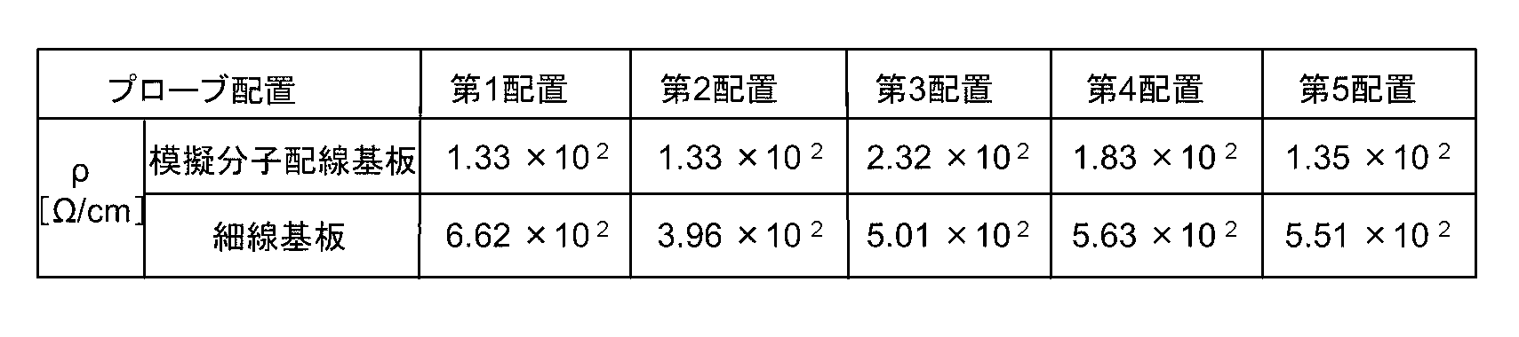
<抵抗値rの評価におけるアルゴリズムの妥当性>
次に、本実施形態の分子配線基板の抵抗値rの評価におけるアルゴリズムの妥当性ついて、説明する。図26は、上述したΔ→Y変換およびY→Δ変換の工程を示す図であって、特に、階数X=2に対応するΔ要素に注目したものである。この工程は、原理的には、図15に示すものと同じであるので、対応する符号はそれぞれ同一とすることで、構成の説明を省略する。変換前においては、頂点をなす電極a、b、cに加え、各辺の中間に電極ab、bc、caが規定される。これら中間の電極ab、bc、ca同士も、相互に伝導する経路が構成される。ここにおいて、実際のモデルとして、電極ab、bc、caは、それぞれΔ要素の外側に対し、分子鎖30ab、30bc、30caとそれぞれ結合されている。また、分子鎖30ab、30bc、30caは、更に外側の電極・分子鎖群と結合されている。従って、電極ab、bc、caは、分子鎖30ab、30bc、30caを介して、Δ要素外側の無数の電極群と接続されていることになる。
次に、本実施形態の分子配線基板の抵抗値rの評価におけるアルゴリズムの妥当性ついて、説明する。図26は、上述したΔ→Y変換およびY→Δ変換の工程を示す図であって、特に、階数X=2に対応するΔ要素に注目したものである。この工程は、原理的には、図15に示すものと同じであるので、対応する符号はそれぞれ同一とすることで、構成の説明を省略する。変換前においては、頂点をなす電極a、b、cに加え、各辺の中間に電極ab、bc、caが規定される。これら中間の電極ab、bc、ca同士も、相互に伝導する経路が構成される。ここにおいて、実際のモデルとして、電極ab、bc、caは、それぞれΔ要素の外側に対し、分子鎖30ab、30bc、30caとそれぞれ結合されている。また、分子鎖30ab、30bc、30caは、更に外側の電極・分子鎖群と結合されている。従って、電極ab、bc、caは、分子鎖30ab、30bc、30caを介して、Δ要素外側の無数の電極群と接続されていることになる。
図26における破線囲み部の等価関係は、分子鎖30ab、30bc、30caによって、階数X=2に対応するΔ要素の外側への接続が考慮されていない。本実施形態のアルゴリズムは、このように「Δ要素の外側への接続が考慮されていない」仮定を採ることで単純化されているが、妥当性を損なうものではない。以下、妥当性についての定量的な評価を行うため、Δ要素の外側への接続を考慮した補正について説明する。
図27は、本実施形態の分子配線基板のモデルを説明する図である。階数X=2に相当する電極群(電極a、b、cおよび電極ab、bc、ca)で構成される三角形を基本として(以下、この三角形を「基本三角形Δbase」と称呼する。)、基本三角形Δbaseの外側における電極・分子鎖の結合が、グロス抵抗値GRに与える影響を算出することで、誤差を定量的に検討した。具体的には、上記基本三角形Δbaseの外側領域の大きさ(外側における電極・分子鎖の結合数と等価)と、グロス抵抗GRとの関係を、シミュレータを用いて算出した。
基本三角形Δbaseの外側領域の大きさを、4種類(Δ0,Δ1,Δ2,Δ3)設定した。ここにおいて、外側領域Δ0,Δ1,Δ2,Δ3は、それぞれ、X=2,X=4,X=6,X=8のΔ要素内側の電極・分子鎖群から基本三角形Δbase分を差し引いた領域に相当している。即ち、Δ0においては、外部領域が実質的には無いことを意味している。
シミュレータとしては、電子回路シミュレータであるLTSpice(登録商標)を用いた。LTSpiceにて、基板の電極20に相当する位置をそれぞれ規定し、その間に仮想の分子鎖30として、抵抗をそれぞれ配置することでネットワーク化した。基本三角形Δbaseと、各外側領域Δ0,Δ1,Δ2,Δ3に対応する抵抗ネットワークモデルを、それぞれ構築した。外側領域Δ0,Δ1,Δ2,Δ3に対応して構築された抵抗ネットワークモデルは、図28、図29、図30、図31にて示される。
ここにおいて、仮想のプローブPを電極bおよび電極cに対応させることとして、グロス抵抗GRを、電極bおよび電極c間から算出した。外側領域の大きさがΔ0,Δ1,Δ2,Δ3のいずれの場合においても、電極間の分子鎖に対応する抵抗を10Ω、電流を100mAとした。
図32は、上記抵抗ネットワークモデルから算出されるグロス抵抗GR(縦軸)と、基本三角形Δbaseの外側領域の大きさ(横軸)との関係を示すグラフである。外側領域Δ0,Δ1,Δ2,Δ3に対応するグロス抵抗GRは、それぞれ、11.1Ω,5.87Ω,5.12Ω,4.88Ωとなった。実線は、この計算値に対応するプロットを結んだものである。なお、破線については、後に詳述する。実線の変化傾向によれば、外側領域Δ1以上となると、グロス抵抗GRの値は、ほぼ収束値に推移していく。
ところで、本実施形態のアルゴリズムを適用する場合について考える。上述のシミュレータ計算では、外側領域を考慮してグロスGRが算出された。一方、本実施形態のアルゴリズムは、外側領域が考慮されない仮定が入る点で、シミュレータ計算と大きく異なる。本実施形態のアルゴリズムによれば、階数X=2に相当するΔ要素(電極a,b,cが頂点の三角形)において、Y⇔Δ変換にて一辺相当の抵抗値が「(5/3)r」となることを説明した(例えば、図26を参照。)。一辺相当の抵抗値が「(5/3)r」であるΔ要素において、シミュレータ計算と同様に、仮想のプローブPを電極bおよび電極cに対応させることとした場合には、グロス抵抗GRと、抵抗値rとの間に、下記式(36)の関係が成立する。
1/GR=1/((5/3)r)+1/((5/3)r+(5/3)r) ・・・(36)
1/GR=1/((5/3)r)+1/((5/3)r+(5/3)r) ・・・(36)
上記式(36)を更に整理すると、グロス抵抗GR=(10/9)rとなる。この式に、r=10Ω(上述のシミュレータ計算における抵抗値と同値)を代入した場合、グロス抵抗GRは、11.1Ωとなる。この値は、上述のシミュレータ計算にて外側領域Δ0とした場合のグロス抵抗GRに一致している。このことは、外側領域Δ0の条件(シミュレータ計算)は、実質的に外側領域を考慮していない仮定(本実施形態のアルゴリズム)と同様であることを意味している。
本実施形態のアルゴリズムにおいては、外側領域を考慮していないので、例えば、外側領域の大きさがΔ0,Δ1,Δ2,Δ3の何れであっても、上記式(36)に則ることになる。従って、r=10Ωである場合、図32の破線に示すように、外側領域の大きさに関わらず、グロス抵抗GRは、11.1Ωの値に推移する。
図32の破線・実線間の乖離は、外側領域の大きさがΔ0,Δ1,Δ2,Δ3とした場合に対応して、それぞれ0%,47%,54%,56%となった。上記実線(グロス抵抗GR)が収束するのに応じて、この乖離もΔ1以上にて収束し得ることが解る。即ち、本実施形態のアルゴリズムによれば、グロス抵抗GR(に基づく抵抗値r)が結果的に略2倍のファクタを含むことになるが、オーダー的には妥当な値であることが解る。
このように、本実施形態のアルゴリズムにおいては、Y⇔Δ変換の際に、上述のように外側領域を考慮しない仮定が含まれ単純化されている。この仮定の下であっても、以上説明した補正の結果、本実施形態のアルゴリズムは妥当であることが示された。
なお、本出願は、2014年7月29日に日本国に本出願人により出願された、特願2014-154107号に基づく。その全内容は、参照により本出願に組み込まれる。
本発明の特定の実施形態についての上記説明は、例示を目的として提示したものである。それらは、網羅的であったり、記載した形態そのままに本発明を制限したりすることを、意図したものではない。数多くの変形や変更が、上記の記載内容に照らして可能であることは、当業者に自明である。
本発明の分子配線基板によれば、分子伝導性の評価に対し、例えば、測定回数が一回であっても、十分な信頼性を得ることができる。この分子配線基板によれば、特別な大型装置を必要とせず、例えば、ラボベンチ上で簡易に分子伝導性を評価できる。従って、市場規模の大きいインターフェイス(分子機能を最大限に活用するもの、例えば、分子センサ(ガスセンサ、バイオセンサなど)の検出デバイス、ナノ・マイクロ流体チップの検出デバイス、分子集積回路の他、架橋分子の熱伝導や応力伝搬などの分子の輸送特性を計測するためのシステムにおけるインターフェイス部材など)に応用され得るので、産業上有用である。
より具体的には、例えば以下の態様にて、分子伝導性が評価され得る。
・分子ワイヤ :真の分子伝導特性
・ダイオード :pn接合の2種連結した分子鎖
・スイッチ :分子鎖に、水酸基、カルボキシル基、アミノ基、光異性化機能基など外場応答する官能基を置換したもの
・トランジスタ:基板への電圧印可による、分子鎖における電界効果、溶液界面の電気二重層制御などによるField Effect Transistor
・分子集積回路:基板上の微小領域において、分子鎖に対して量産可能なオンチップ修飾・加工(化学的修飾または物理的加工、例えば、極細ビーム描画、フォトリソグラフィによる領域選択的なもの)したもの。
・分子ワイヤ :真の分子伝導特性
・ダイオード :pn接合の2種連結した分子鎖
・スイッチ :分子鎖に、水酸基、カルボキシル基、アミノ基、光異性化機能基など外場応答する官能基を置換したもの
・トランジスタ:基板への電圧印可による、分子鎖における電界効果、溶液界面の電気二重層制御などによるField Effect Transistor
・分子集積回路:基板上の微小領域において、分子鎖に対して量産可能なオンチップ修飾・加工(化学的修飾または物理的加工、例えば、極細ビーム描画、フォトリソグラフィによる領域選択的なもの)したもの。
更に、上述したアルゴリズムは、分子伝導性にかかる全ての輸送現象に適用できる。即ち、分子鎖あたりの熱伝導、イオン伝導、応力伝搬などの輸送特性が、例えば、1回の測定で得られる。
Claims (13)
- 基板と、
前記基板上に、間隔をもって相互離間するとともに、所定の規則をもって無数に配設された電極と、
前記電極のうち隣り合う前記電極間の伝導を許容するように前記隣り合う前記電極間を架橋する、所定の分子の集合体にて構成される分子鎖と、
を備えた分子配線基板であって、
前記分子鎖は、
前記架橋を達成するために、前記電極が前記基板上へ配設された後に、前記所定の分子の一部を前記電極に接合し、前記一部の分子を起端・終端として残りの分子を重合または自己組織化することで構成され、
前記所定の分子に対して、分光分析を実施した場合において、
前記電極への接合後であって前記重合および前記自己組織化のいずれも開始されていない状態での前記分光分析の実施により検出されるスペクトルである開始前スペクトルと、
前記重合または前記自己組織化の開始後での前記分光分析の実施により検出されるスペクトルである開始後スペクトルとの所定の差異に基づいて、前記隣り合う前記電極間における前記分子鎖の架橋数が決定され、
前記隣り合う前記電極の間隔よりも大きい間隔である検出間隔の両端点にて検出される抵抗値と、
前記検出間隔と、
前記隣り合う前記電極の間隔と、
に基づいて、
前記隣り合う前記電極の間隔における抵抗値が決定され、
前記決定された架橋数と、前記決定された抵抗値とに基づいて、前記電極の間隔における前記分子鎖の伝導性を決定することを特徴とする分子配線基板。 - 請求項1に記載の分子配線基板において、
前記分光分析は、ラマン分光分析または蛍光分光分析であり、
前記開始前スペクトルおよび前記開始後スペクトルは、前記分光分析が前記ラマン分光分析である場合には、振動スペクトルであり、前記分光分析が前記蛍光分光分析である場合には、電子スペクトルであることを特徴とする分子配線基板。 - 請求項2に記載の分子配線基板において、
前記分光分析は、前記ラマン分光分析であり、
前記開始前スペクトルおよび前記開始後スペクトルにおける前記所定の差異は、
前記開始前スペクトルにおける前記接合された分子の振動に対応するピークである開始前ピークの強度と、前記開始後スペクトルにおける前記接合された分子の振動に対応するピークである開始後ピークの強度との差異であることを特徴とする分子配線基板。 - 請求項3に記載の分子配線基板において、
前記開始前ピークおよび前記開始後ピークは、それぞれの波数が同一となるものが用いられ、
前記分子鎖の架橋数は、
前記開始前ピークおよび前記開始後ピークの強度の差異が大きいほど、より大きい数に決定されることを特徴とする分子配線基板。 - 請求項4に記載の分子配線基板において、
前記分子鎖は、前記分子を重合することで構成され、
前記開始後スペクトルは、前記重合の開始後であって前記重合の完了後に、前記ラマン分光分析が実施されることで取得され、
前記開始前ピークおよび前記開始後ピークは、前記電極に接合された分子であって前記重合の終端となる分子の振動に対応するとともに、前記開始前ピークの強度が前記開始後ピークの強度よりも大きいものを用いることを特徴とする分子配線基板。 - 請求項1乃至請求項5の何れか一項に記載の分子配線基板において、
前記分子鎖は、前記分子を重合することで構成され、
前記電極に接合する分子であって前記重合の起端となる分子は、表面開始剤であり、
前記電極に接合する分子であって前記重合の終端となる分子は、表面停止剤であり、
前記表面開始剤、および前記表面停止剤は、
炭素-炭素間に3重結合を少なくとも1つ備えるとともに、前記3重結合にかかる炭素を介し、前記電極と接合されることを特徴とする分子配線基板。 - 請求項6に記載の分子配線基板において、
前記分子鎖の架橋数は、
前記開始前スペクトルおよび前記開始後スペクトルの前記所定の差異と、更に、前記電極に接合された前記表面開始剤および/または前記表面停止剤の接合数とに基づいて決定され、
前記接合数は、
前記表面開始剤および/または前記表面停止剤に対して、前記分光分析を実施した場合において、
前記基板への前記電極の配設後であって、前記電極への前記表面開始剤および前記表面停止剤がいずれも接合されていない状態での前記分光分析の実施により検出されるスペクトルである接合前スペクトルと、
前記電極への前記表面開始剤および/または前記表面停止剤が接合された後であって、前記重合が開始されていない状態での前記分光分析の実施により検出されるスペクトルである接合後スペクトルとの所定の差異に基づいて決定されることを特徴とする分子配線基板。 - 請求項6又は請求項7に記載の分子配線基板において、
前記分子鎖は、パイ共役系高分子で構成されることを特徴とする分子配線基板。 - 請求項8に記載の分子配線基板において、
前記分光分析は、
ラマン分光分析であり、
前記開始前スペクトル、前記開始後スペクトル、前記接合前スペクトル、および前記接合後スペクトルは、
振動スペクトルであり、
前記開始後スペクトルは、
前記重合の開始後であって前記重合の完了後に、前記ラマン分光分析が実施されることで取得され、
前記開始前スペクトルおよび前記開始後スペクトルにおける前記所定の差異は、
前記開始前スペクトルにおける前記表面停止剤の前記3重結合にかかる炭素の振動に対応するピークである開始前ピークの強度と、前記開始後スペクトルにおける前記表面停止剤の前記3重結合にかかる炭素の振動に対応するピークである開始後ピークの強度との差異であり、
前記接合前スペクトルおよび前記接合後スペクトルにおける前記所定の差異は、
前記接合前スペクトルにおける前記表面停止剤の前記3重結合にかかる炭素の振動に対応するピークである接合前ピークの強度と、前記接合後スペクトルにおける前記表面停止剤の前記3重結合にかかる炭素の振動に対応するピークである接合後ピークの強度との差異であり、
前記接合数は、
前記接合前ピークおよび前記接合後ピークの強度の差異が大きいほど、より大きい数に決定され、
前記分子鎖の架橋数は、
前記開始前ピークおよび前記開始後ピークの強度の差異が大きいほど、より大きい数に決定されることを特徴とする分子配線基板。 - 請求項1乃至請求項9の何れか一項に記載の分子配線基板において、
前記電極は、
前記所定の規則として、前記分子鎖が前記電極に架橋したときに三角格子が形成されるよう配設され、
前記隣り合う前記電極の間隔における抵抗値は、
前記検出間隔の両端点にて検出される抵抗値をGR、前記検出間隔をD、前記隣り合う前記電極の間隔をd、前記隣り合う前記電極の間隔における抵抗値をr、係数をJ,Kとした場合に、
logGR=(J)log(D/d)+log(Kr)なる関係式を用いて決定されることを特徴とする分子配線基板。 - 請求項10に記載の分子配線基板において、
前記検出間隔の両端点にて検出される抵抗値は、
各先端で、前記検出間隔に相当するよう相互離間した2つの針状プローブであって、前記各先端を前記電極に近接させることで、前記各先端の間隔に対応する抵抗値を検出するプローブにて検出される抵抗値であることを特徴とする分子配線基板。 - 請求項1乃至請求項11の何れか一項に記載の分子配線基板において、
前記電極は、
その形状および配列が規定のものとなるよう、前記形状および前記配列に対応する空間を有するテンプレートを用いて、前記基板上に配設されることを特徴とする分子配線基板。 - 請求項12に記載の分子配線基板において、
前記テンプレートは、
材料として、ポリエチレンオキサイド-ポリメタクリレート誘導体ブロック共重合体、又は、ポリスチレン-ポリ(4-ビニリピリジン)ブロック共重合体を用いるよう構成され、
前記電極は、
材料として、金、銀、および銅のうち少なくとも1つの元素を用い、各々ドット形状に構成されるとともに、前記隣り合う前記電極の間隔の距離範囲が5乃至50ナノメートルとなるよう構成されたことを特徴とする分子配線基板。
Applications Claiming Priority (2)
| Application Number | Priority Date | Filing Date | Title |
|---|---|---|---|
| JP2014154107A JP2017166821A (ja) | 2014-07-29 | 2014-07-29 | 分子配線基板 |
| JP2014-154107 | 2014-07-29 |
Publications (1)
| Publication Number | Publication Date |
|---|---|
| WO2016017522A1 true WO2016017522A1 (ja) | 2016-02-04 |
Family
ID=55217423
Family Applications (1)
| Application Number | Title | Priority Date | Filing Date |
|---|---|---|---|
| PCT/JP2015/070966 Ceased WO2016017522A1 (ja) | 2014-07-29 | 2015-07-23 | 分子配線基板 |
Country Status (2)
| Country | Link |
|---|---|
| JP (1) | JP2017166821A (ja) |
| WO (1) | WO2016017522A1 (ja) |
Cited By (1)
| Publication number | Priority date | Publication date | Assignee | Title |
|---|---|---|---|---|
| CN115955899A (zh) * | 2023-01-16 | 2023-04-11 | 浙江师范大学 | 一种基于局域阳离子调控的可逆单分子开关 |
Citations (3)
| Publication number | Priority date | Publication date | Assignee | Title |
|---|---|---|---|---|
| JP2010073916A (ja) * | 2008-09-19 | 2010-04-02 | Sony Corp | 分子素子およびその製造方法ならびに集積回路装置およびその製造方法ならびに三次元集積回路装置およびその製造方法 |
| JP5313664B2 (ja) * | 2006-04-19 | 2013-10-09 | 独立行政法人科学技術振興機構 | 表面に微小金属塊が整列した基板の製法 |
| WO2015079824A1 (ja) * | 2013-11-26 | 2015-06-04 | 国立大学法人東京工業大学 | パイ共役系高分子およびそのパイ共役系高分子を備えるブロック共重合体 |
-
2014
- 2014-07-29 JP JP2014154107A patent/JP2017166821A/ja active Pending
-
2015
- 2015-07-23 WO PCT/JP2015/070966 patent/WO2016017522A1/ja not_active Ceased
Patent Citations (3)
| Publication number | Priority date | Publication date | Assignee | Title |
|---|---|---|---|---|
| JP5313664B2 (ja) * | 2006-04-19 | 2013-10-09 | 独立行政法人科学技術振興機構 | 表面に微小金属塊が整列した基板の製法 |
| JP2010073916A (ja) * | 2008-09-19 | 2010-04-02 | Sony Corp | 分子素子およびその製造方法ならびに集積回路装置およびその製造方法ならびに三次元集積回路装置およびその製造方法 |
| WO2015079824A1 (ja) * | 2013-11-26 | 2015-06-04 | 国立大学法人東京工業大学 | パイ共役系高分子およびそのパイ共役系高分子を備えるブロック共重合体 |
Non-Patent Citations (3)
| Title |
|---|
| SHINGO HADANO ET AL.: "Block Copolymer Template-ho de Sakusei shita Kin Nano Ryushi Array no Hyomen Zokyo Raman Koka to Bunshi Sensing eno Oyo", DAI 61 KAI SYMPOSIUM ON MACROMOLECULES, 19 September 2012 (2012-09-19), Yokoshu, pages 4045 * |
| TATSUYA KONISHI ET AL.: "Single Molecule Dynamics at a Mechanically Controllable Break Junction in Solution at Room Temperature", JOURNAL OF THE AMERICAN CHEMICAL SOCIETY, vol. 135, 2012, pages 1009 - 1014 * |
| WEI ZOU ET AL.: "Solvent induced formation of an ordered nanorod array of gold/polymer composite by block copolymer film templating", NANOTECHNOLOGY, vol. 22, 2011, pages 335301.1 - 335301.6 * |
Cited By (1)
| Publication number | Priority date | Publication date | Assignee | Title |
|---|---|---|---|---|
| CN115955899A (zh) * | 2023-01-16 | 2023-04-11 | 浙江师范大学 | 一种基于局域阳离子调控的可逆单分子开关 |
Also Published As
| Publication number | Publication date |
|---|---|
| JP2017166821A (ja) | 2017-09-21 |
Similar Documents
| Publication | Publication Date | Title |
|---|---|---|
| Magyarkuti et al. | Electronic and mechanical characteristics of stacked dimer molecular junctions | |
| Bergren et al. | Musical molecules: the molecular junction as an active component in audio distortion circuits | |
| JP5016649B2 (ja) | センサ | |
| KR101737525B1 (ko) | 나노크랙을 이용한 고 민감도, 고 변형율 측정센서 및 그 제조방법 및 변형율 측정 시스템 | |
| Brophy et al. | Ultra Responsive NO2 silicon nanowires gas sensor | |
| Guselnikova et al. | Large‐Scale, Ultrasensitive, Highly Reproducible and Reusable Smart SERS Platform Based on PNIPAm‐Grafted Gold Grating | |
| Jiang et al. | Ordered‐assembly conductive nanowires array with tunable polymeric structure for specific organic vapor detection | |
| Wang et al. | Direct‐print 3D electrodes for large‐scale, high‐density, and customizable neural interfaces | |
| Mohan et al. | Risk assessment of a multiplexed carbon nanotube network biosensor | |
| Aragones et al. | Nearfield trapping increases lifetime of single-molecule junction by one order of magnitude | |
| US20160341688A1 (en) | Method of manufacturing nano gap sensor using residual stress and nano gap sensor manufactured thereby | |
| CN103134456B (zh) | 膜厚测量方法及膜厚测量装置、半导体集成电路的制造方法 | |
| WO2016017522A1 (ja) | 分子配線基板 | |
| CN110632126A (zh) | 一种有机磷化合物传感器及其制备方法 | |
| Mondal et al. | Fabrication and packaging of MEMS based platform for hydrogen sensor using ZnO–SnO2 composites | |
| Cho et al. | Nanoscale mapping of molecular vibrational modes via vibrational noise spectroscopy | |
| Koecher et al. | Characterization of nickel nanostrand nanocomposites through dielectric spectroscopy and nanoindentation | |
| JP5288120B2 (ja) | ガスセンサ及びガス検出装置 | |
| CN110174185B (zh) | 表征有基底纳米线的空间扫描双波长拉曼闪光方法及装置 | |
| US20190086458A1 (en) | System and method for non-contact measurement of optoelectronic properties of thin film | |
| Lillemose et al. | Epoxy based photoresist/carbon nanoparticle composites | |
| Rastegar et al. | Measurement of signal‐to‐noise ratio in graphene‐based passive microelectrode arrays | |
| Savu et al. | Gas sensors based on locally heated multiwall carbon nanotubes decorated with metal nanoparticles | |
| US7816906B2 (en) | Method for determining anisotropy of 1-D conductor or semiconductor synthesis | |
| CN205898685U (zh) | 一种一次性使用的表面增强拉曼光谱芯片 |
Legal Events
| Date | Code | Title | Description |
|---|---|---|---|
| 121 | Ep: the epo has been informed by wipo that ep was designated in this application |
Ref document number: 15827649 Country of ref document: EP Kind code of ref document: A1 |
|
| NENP | Non-entry into the national phase |
Ref country code: DE |
|
| 122 | Ep: pct application non-entry in european phase |
Ref document number: 15827649 Country of ref document: EP Kind code of ref document: A1 |
|
| NENP | Non-entry into the national phase |
Ref country code: JP |