WO2016009503A1 - 受信回路、送信回路、情報処理装置、システム、および伝送方法 - Google Patents
受信回路、送信回路、情報処理装置、システム、および伝送方法 Download PDFInfo
- Publication number
- WO2016009503A1 WO2016009503A1 PCT/JP2014/068868 JP2014068868W WO2016009503A1 WO 2016009503 A1 WO2016009503 A1 WO 2016009503A1 JP 2014068868 W JP2014068868 W JP 2014068868W WO 2016009503 A1 WO2016009503 A1 WO 2016009503A1
- Authority
- WO
- WIPO (PCT)
- Prior art keywords
- data
- code
- reception
- unit
- clock
- Prior art date
- Legal status (The legal status is an assumption and is not a legal conclusion. Google has not performed a legal analysis and makes no representation as to the accuracy of the status listed.)
- Ceased
Links
Images










Classifications
-
- G—PHYSICS
- G06—COMPUTING OR CALCULATING; COUNTING
- G06F—ELECTRIC DIGITAL DATA PROCESSING
- G06F13/00—Interconnection of, or transfer of information or other signals between, memories, input/output devices or central processing units
- G06F13/38—Information transfer, e.g. on bus
- G06F13/42—Bus transfer protocol, e.g. handshake; Synchronisation
-
- H—ELECTRICITY
- H04—ELECTRIC COMMUNICATION TECHNIQUE
- H04L—TRANSMISSION OF DIGITAL INFORMATION, e.g. TELEGRAPHIC COMMUNICATION
- H04L7/00—Arrangements for synchronising receiver with transmitter
Definitions
- the present invention relates to a receiving circuit, a transmitting circuit, an information processing apparatus, a system, and a transmission method. About.
- a difference adjustment code string (SKIP order set) is inserted.
- SKIP order set is composed of specific special data strings, and is different from other special data strings and valid data.
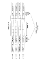
- FIG. 1 is a diagram showing a conventional SKIP order set.
- the SKIP order set is inserted between valid data among the data received by the receiving side.
- the SKIP order set is composed of a COM symbol and two SKP symbols.
- two SKP symbols are arranged immediately after the COM symbol.
- the COM symbol is a symbol arranged at the head of the SKIP order set.
- the SKP symbol is a symbol used for adjusting the frequency difference by addition or deletion on the reception side.
- the data receiving circuit operates at the pace of the received data (hereinafter referred to as receiving clock), and when it detects the SKIP order set, it expands / contracts (adds or deletes) the absorption code (SKP symbol).
- the transfer rate is adjusted to the clock (hereinafter referred to as internal clock).
- FIG. 2A is a diagram showing frequency difference adjustment processing using a conventional SKIP order set.
- the top data in FIG. 2A indicates data received by the receiving side as in FIG. As described in FIG. 1, a SKIP order set (COM symbol and two SKP symbols) is inserted between valid data.
- the SKIP order set is further added as shown in the second data from the top in FIG. 2A. Add the SKP symbol to delay the timing to pass to the subsequent circuit.
- the SKP symbol is deleted from the SKIP order set as shown in the third data from the top in FIG. Make the timing of passing faster.
- the SKIP order set is left as it is as shown in the fourth data from the top in FIG. 2A.
- a technique is known in which a transmission unit inserts a SKIP order set into a data packet and transmits the data packet to a reception unit, and the reception unit inserts or deletes an SKP character so as to absorb a frequency difference (for example, Patent Documents). 1).
- the SKIP order set is detected, and the SKP symbol in the SKIP order set is added and deleted based on the timing error between the reception clock and the internal clock.
- the SKIP order set including the first COM symbol to the last SKP symbol needs to stay in the vicinity of the processing circuit that performs addition / deletion of the SKP symbol until the addition / deletion of the SKP symbol is performed.
- causes delay
- an object of the present invention is to reduce a transfer delay (latency) for adjusting a frequency difference in a circuit.
- the receiving circuit includes a detection unit, a determination unit, and a code length control unit.
- the detection unit detects a start code indicating the start of the frequency difference adjustment code string from the received data.
- the determination unit determines a timing error between the reception clock and the internal clock.
- the code length control unit is configured to adjust the length of the adjustment code inserted at a position away from the position where the start code is detected in the received data by a specified distance according to the timing error determined by the determination unit. Adjust the height.
- the transfer delay in the circuit can be reduced.
- FIG. 1 is a configuration diagram of a system according to an embodiment.
- 2 is a configuration diagram of a transmission LSI and a reception LSI according to an embodiment.
- FIG. It is a block diagram of the transmission lane process part which concerns on embodiment.
- FIG. 2B is a diagram illustrating an example of the configuration and processing of the receiving LSI.
- the receiving LSI 10 is connected to a transmitting LSI (not shown) by four lanes k (not shown).
- the reception lane processing unit 11-k receives the data transmitted via the lane k and processes the data.
- FIG. 2B only the configuration of the reception lane processing unit 11-3 is described in detail. Since the configuration of the reception lane processing units 11-0 to 11-2 is the same as that of the reception lane processing unit 11-3, description thereof is omitted.
- the reception lane processing unit 11-3 includes a reception unit 12, flip-flops 13-1, 13-2, and 13-3, a SKIP order set detection unit 14, a data addition / deletion processing unit 15, and a clock transfer buffer 16.
- the receiving unit 12 receives data from the transmission LSI, performs processing such as serial / parallel conversion, and outputs the data to the flip-flop 13-1.
- the flip-flops 13-1, 13-2, and 13-3 hold the input data and output the data in synchronization with the reception clock.
- the data is data for one symbol.
- the flip-flop 13-1 outputs the data to the SKIP order set detection unit 14 and the flip-flop 13-2.
- the flip-flop 13-2 outputs the data to the SKIP order set detection unit 14 and the flip-flop 13-3.
- the flip-flop 13-3 outputs the data to the clock transfer buffer 16.
- the SKIP order set detection unit 14 checks the data input from the flip-flops 13-1 and 13-2 and detects the SKIP order set. When detecting the SKIP order set, the SKIP order set detection unit 14 notifies the reception control unit 21 of the detection of the SKIP order set.
- the receiving unit 12, the flip-flops 13-1, 13-2, 13-3, and the SKIP order set detecting unit 14 operate in synchronization with the reception clock.
- the data addition / deletion processing unit 15 adds or deletes an SKP symbol based on an instruction from the reception control unit 21. Specifically, for example, the data addition / deletion processing unit 15 adjusts the read pointer of the clock transfer buffer 16 based on an instruction from the reception control unit.
- the reception control unit 21 receives the notification from the SKIP order set detection unit 14 of each reception lane processing unit 11-k, and adds or deletes the SKP symbol to the data addition / deletion processing unit 15 of each reception lane processing unit 11-k. Give instructions.
- the frequency difference absorption operation described in the background art consists of two phases: (1) “Detect SKIP order set” and (2) “Add or delete SKP symbols as necessary as a result of detection”. In the received data stream (stream), this must be executed in order for the same part (the part of the SKIP order set).
- the process (1) is performed by the SKIP order set detection unit 14, and the process (2) is performed by the data addition / deletion processing unit 15.
- a plurality of serial transmissions are bundled into a unit having a certain width, and data is often handled in that unit inside the LSI (before the receiving unit).
- a code is added to the SKIP order set sent simultaneously to the reception lane processing unit 11-k. It is necessary to determine whether to add or delete the data in synchronization with each other between the reception lane processing units 11-k.
- the data in the part is a circuit that performs those processes until the process of (2) is completed. It is necessary to stay in the vicinity (the flip-flop 13 and the clock transfer buffer 16).
- FIG. 3 is a diagram showing a SKIP order set according to the embodiment.
- the SKIP order set of the embodiment includes a detection part (A) and an expansion / contraction part (B).
- the SKIP order set is an example of a frequency difference adjustment code string.
- the detection part (A) is composed of one COM symbol and one SKP symbol.
- the SKP symbol is arranged immediately after the COM symbol.
- the detection part is an example of a start code.
- Extensible part (B) is composed of one SKP symbol.
- the stretchable part (B) is an example of an adjustment code.
- the detection part (A) and the expansion / contraction part (B) are arranged apart by a distance N (number of symbols).
- the distance N may be a fixed symbol length, may be specified according to a predefined symbol included in the detection portion, or obtained from data between the detection portion (A) and the stretchable portion (B). It may be calculated from the packet length information.
- Valid data (payload) or invalid data is inserted between the detection part (A) and the expansion / contraction part (B).
- FIG. 4 is a configuration diagram of a system according to the embodiment.
- CPU central processing unit
- XB crossbar switch
- I / O adapter 204-ik 0-3.
- the CPU 202-i-1 and the CPU 202-i-2 are connected by a plurality of lanes (serial buses).
- CPU 202-i-j and XB 203-i are connected by a plurality of lane serial buses.
- XB 203-1 and XB 203-2 are connected by a plurality of lanes (serial buses).
- the CPU 202-ij is a processing device that performs various processes.
- the XB 203-i is a switch that dynamically selects a data path.
- the XB 203-i receives the packet from the XB 203-i or the CPU 202-ij, recognizes the destination included in the packet, and transfers it to the transmission destination.
- the transmission LSI and the reception LSI are mounted on the CPUs 202-ij and XB203-i, and are used for communication between the CPU and CPU, between the CPU and XB, and between XB and XB.
- FIG. 5 is a configuration diagram of a transmission LSI and a reception LSI according to the embodiment.
- the reception LSI 401 includes a reception lane processing unit 411-k, a reception control unit 421, and a reception packet analysis unit 431.
- the transmission LSI 301 is connected to the reception LSI 401 through four lanes (serial bus).
- the transmission lane processing unit 321-k is connected to the reception lane processing unit 411-k via the lane.
- a lane connecting the transmission lane processing unit 321 -k and the reception lane processing unit 411 -k is denoted as lane k.
- the transmission packet generation unit 311 generates a transmission packet to be transmitted to the reception LSI, and divides the transmission packet and transmits it to the transmission lane processing unit 321 -k.
- the transmission lane processing unit 321-k generates a SKIP order set, inserts the SKIP order set into the input packet, and transmits it to the reception lane processing unit 411-k. Details of the transmission lane processing unit 321 -k will be described later.
- the reception lane processing unit 411-k detects the detection part of the SKIP order set and the distance N from the input data, and notifies the reception control unit 421 of it.
- the reception lane processing unit 411-k adds or deletes the expansion / contraction portion (SKP symbol) of the SKIP order set based on an instruction from the reception control unit 421. Details of the reception lane processing unit 411-k will be described later.
- the reception lane processing unit 411-k outputs the reception packet to the reception packet analysis unit 431.
- the reception control unit 421 determines an error between the reception clock and the internal clock, that is, a frequency difference between the reception clock and the internal clock.
- the reception control unit 421 instructs the reception lane processing unit 411-k to add or delete the expansion / contraction part based on the determined error and the notification of the reception lane processing unit 411-k.
- the reception control unit 421 is an example of a code length control unit.
- the reception clock is generated by clock data recovery of the reception data.
- the internal clock is generated by a clock generation circuit (not shown) in the reception LSI 401.
- the received packet analysis unit 431 performs processing such as analysis on the packet input from the transmission lane processing unit 411-k.
- the received packet analysis unit 431 is an example of a data processing unit.
- FIG. 6 is a configuration diagram of a transmission lane processing unit according to the embodiment.
- the transmission lane processing unit 321-k includes a SKIP order set generation unit 322-k and a parallel / serial conversion circuit 323-k.
- the SKIP order set generation unit 322-k generates, for example, the SKIP order set shown in FIG. 3, inserts the SKIP order set between the input packets, and outputs it to the parallel / serial conversion circuit 323-k.
- the parallel / serial conversion circuit 323-k mutually converts parallel data and serial data.
- the parallel / serial conversion circuit 323-k converts the input parallel data into serial data, and outputs the serial data to the reception lane processing unit 411-k via the lane k.
- FIG. 7 is a configuration diagram of a reception lane processing unit according to the embodiment.
- the reception lane processing unit 411-k includes a parallel / serial conversion circuit 412-k, a SKIP order set detection unit 413-k, and a clock transfer buffer 414-k.
- the parallel / serial conversion circuit 412-k converts parallel data and serial data to each other.
- the parallel / serial conversion circuit 412-k converts the input serial data into parallel data, and outputs the parallel data to the SKIP order set detection unit 413-k and the clock transfer buffer 414-k.
- the SKIP order set detection unit 413-k detects the detected part of the SKIP order set and the distance N, and notifies the reception control unit 421 of it.
- the clock transfer buffer 414-k is a buffer used for transfer from the reception clock to the internal clock. That is, the clock transfer buffer 414-k writes data using the reception clock and reads data using the internal clock.
- the clock transfer buffer 414-k is a buffer for adjusting a frequency difference by adding or deleting an SKP symbol.
- FIG. 8 is a flowchart of a transmission process according to the embodiment. Steps S501, S502, S504, S505, and S507 are executed in each transmission lane processing unit 321-k.
- step S501 the transmission lane processing unit 321-k determines whether a SKIP order set transmission instruction has been received from the transmission packet generation unit 311. If received, the control proceeds to step S502. If not received, it waits until it receives a SKIP order set transmission instruction.
- step S502 the transmission lane processing unit 321-k receives the notification of the distance N from the transmission packet generation unit 311. If the distance N is a fixed symbol length, that is, if the distance N is determined in advance, the processing in step 502 may be omitted.
- step S503 the transmission packet generation unit 311 creates a gap enough to insert the detection part.
- step S504 the transmission lane processing unit 321-k inserts the detection portion into the input packet and transmits the packet to the reception lane processing unit 411-k.
- step S505 the transmission lane processing unit 321-k receives the filling packet (that is, valid data) from the transmission packet generation unit 311 and transmits it to the reception lane processing unit 411-k.
- step S506 the transmission packet generation unit 311 creates a gap for inserting the expansion / contraction portion.
- step S507 the transmission lane processing unit 321-k inserts an expansion / contraction part into the input packet and transmits the packet to the reception lane processing unit 411-k.
- FIG. 9 is a flowchart of a reception process according to the embodiment. Steps S601 to S603, S606, and S607 are executed in each reception lane processing unit 411-k.
- step S601 the SKIP order set detection unit 413-k checks the input data, and if the detection part (A) is detected, the control proceeds to step S602.
- the SKIP order set detection unit 413-k specifies the distance N.
- the SKIP order set detection unit 413-k specifies the distance N from the type of the detection portion (A) and data between the detection portion (A) and the expansion / contraction portion (B). If the distance N is a fixed symbol length, that is, if the distance N is determined in advance, the processing in step 602 may be omitted.
- step S603 the SKIP order set detection unit 413-k notifies the reception control unit 421 of the detection of the detection portion (A) and the distance N.
- step S604 the reception control unit 421 waits for synchronization between lanes. That is, the reception control unit 421 waits for notifications from all the SKIP order set detection units 413-k, and when receiving notifications from all the SKIP order set detection units 413-k, the control proceeds to step S605.
- the transmission LSI 301 and the reception LSI 401 a plurality of lanes are bundled into a unit having a certain width, and data is often handled in the unit inside the reception LSI 301 (after the reception lane processing unit 411-k). .
- step S604 In order to prevent misalignment between lanes when processing SKP symbols among a plurality of lanes as a unit, synchronization waiting between lanes is performed in step S604. If synchronization between lanes is unnecessary, step S604 may be omitted.
- step S605 the reception control unit 421 determines a timing error (frequency difference between the reception clock and the internal clock) between the reception clock and the internal clock, and expands / contracts to each reception lane processing unit 411-k based on the determination result.
- An instruction to add or delete the SKP symbol of part (B) is given.
- the reception control unit 421 notifies the distance N to each reception lane processing unit 411-k. When the distance N is a fixed symbol length, the reception control unit 421 does not need to notify the distance N.
- step S606 the reception lane processing unit 411-k adjusts the timing for adding or deleting the SKP symbol to the expansion / contraction part (B) received after a distance N from the detection part (A).
- step S607 the reception lane processing unit 411-k adds or deletes the SKP symbol to the expansion / contraction portion (B).
- FIG. 10 is a diagram illustrating a configuration and processing of the reception LSI according to the embodiment.
- FIG. 10 only the configuration of the reception lane processing unit 411-3 is described in detail. Since the configuration of the reception lane processing units 411-0 to 411-2 is the same as the configuration of the reception lane processing unit 411-3, description thereof is omitted.
- the reception lane processing unit 411-3 includes a reception unit 415-3, flip-flops 416-3-1 and 416-3-2, a SKIP order set detection unit 413-3, a data addition / deletion processing unit 417-3, and a clock transfer.
- a buffer 414-3 is provided.
- the reception unit 415-3 receives data from the transmission LSI 301, performs processing such as serial / parallel conversion on the data, and outputs the data to the flip-flop 416-3-1 and the clock transfer buffer 414-3.
- the receiving unit 415-3 generates a reception clock from the reception data by clock data recovery.
- the receiving unit 415-3 includes the serial / parallel conversion circuit 412-3 of FIG.
- the flip-flops 416-3-1 and 416-3-2 hold the input data and output the data in synchronization with the reception clock.
- the data is data for one symbol.
- the flip-flop 416-3-1 outputs the data to the SKIP order set detection unit 413-3 and the flip-flop 416-3-2.
- the flip-flop 416-3-2 outputs the data to the SKIP order set detection unit 413-3.
- the SKIP order set detection unit 413-3 checks data input from the flip-flops 416-3-1 and 416-3-2, and detects a detection part of the SKIP order set. For example, the SKIP order set detection unit 413-3 detects the detection portion (A) when the input from the flip-flop 416-3-1 is an SKP symbol and the input from the flip-flop 416-3-2 is a COM symbol. To do. When detecting the detection part (A), the SKIP order set detection unit 413-3 notifies the reception control unit 421 of the detection of the detection part (A). The SKIP order set detection unit 413-3 may identify the distance N and notify the reception control unit 421 of it.
- the reception unit 415-3, the flip-flops 416-3-1 and 416-3-2, and the SKIP order set detection unit 413-3 operate in synchronization with the reception clock.
- the data addition / deletion processing unit 417-3 adds or deletes the SKP symbol of the expansion / contraction portion (B) based on an instruction from the reception control unit 421. Specifically, for example, the data addition / deletion processing unit 417-3 adjusts the read pointer of the clock transfer buffer 414-3 based on an instruction from the reception control unit.
- the clock transfer buffer 414-3 writes data in synchronization with the reception clock, reads data in synchronization with the internal clock, and passes the read data to the reception packet analysis unit 431 in the subsequent stage.
- the above-described processing (1) ⁇ (1 ′) ⁇ (2) needs to be performed in the expansion / contraction processing as in the conventional case.
- the detection portion (A) is not necessary and the expansion / contraction portion (B) to be expanded / contracted passes through the vicinity of the expansion / contraction circuit (clock transfer buffer 414). If you do.
- the detection part (A) is not used after it has been detected that it is a SKIP order set, so it can be discarded and does not hinder prompt data transfer (pipelining). Before the process of expanding / contracting the SKP symbol is completed, at least a part of the data between the detection part (A) and the expansion / contraction part (B) is sent to the received packet analysis unit 431 at the subsequent stage for processing. Data transfer is possible.
- the distance N between the detection part (A) and the expansion / contraction part (B) is a number exceeding the number of symbols passing through the corresponding part during the process of (1) ⁇ (1 ′) ⁇ (2). By doing so, it is possible not to interfere with the processing pipeline.
- FIG. 11 is a diagram showing a frequency difference adjustment process between the conventional SKIP order set and the SKIP order set according to the embodiment.
- FIG. 11 shows frequency difference adjustment processing using a conventional SKIP order set
- the lower half of FIG. 11 shows frequency difference adjustment processing using the SKIP order set of the embodiment.
- the top data in FIG. 11 indicates data received by the conventional receiving side as in FIG. As described in FIG. 1, a SKIP order set (COM symbol and two SKP symbols) is inserted between valid data.
- the second and third data from the top of the upper half of FIG. 11 indicate data when the received data is relatively fast and when the received data is relatively slow in the transfer from the received clock to the internal clock, respectively.
- the SKP symbol is added when the received data is relatively fast, and the SKP symbol is added when the received data is relatively slow.
- the top data indicates data received by the receiving side in the same embodiment as in FIG.
- the SKIP order set of the embodiment includes a detection part (one COM symbol and one SKP symbol) and an expansion / contraction part (one SKP symbol).
- the stretchable part is arranged at a distance N from the stretchable part.
- Valid data (payload) is inserted between the detection portion and the expansion / contraction portion.
- the second and third data from the top are the data when the received data is relatively fast and when the received data is relatively slow in the transfer from the received clock to the internal clock, respectively. Show.
- the transfer delay in the circuit can be reduced.
- FIG. 12A shows transmission data transmitted from lane 0 to lane 3 in order from the top.
- the detection part is composed of COM symbols and SKP-A symbols.
- the distance between the detection part and the expansion / contraction part is 6.
- Valid data is inserted between the detection portion and the expansion / contraction portion.
- FIG. 12B shows transmission data transmitted from Lane 0 to Lane 3 in order from the top.
- the detection part is composed of COM symbols and SKP-B symbols.
- the distance between the detection part and the expansion / contraction part is 8.
- Valid data is inserted between the detection portion and the expansion / contraction portion.
- FIG. 12C shows transmission data transmitted from Lane 0 to Lane 3 in order from the top.
- the detection part is composed of COM symbols and SKP-C symbols.
- the distance between the detection part and the expansion / contraction part is 10.
- Valid data is inserted between the detection portion and the expansion / contraction portion.
- FIG. 12D shows transmission data transmitted from lane 0 to lane 3 in order from the top.
- the detection part is composed of COM symbols and SKP-D symbols.
- the distance between the detection part and the expansion / contraction part is 12.
- Valid data is inserted between the detection portion and the expansion / contraction portion.
- the configuration of the detection portion corresponding to the distance as described above is defined in advance.
- the SKP-A symbol, SKP-B symbol, SKP-C symbol, and SKP-D symbol are defined in advance as data.
- the SKP-A symbol, SKP-B symbol, SKP-C symbol, and SKP-D symbol may be arbitrary data as long as they can be distinguished from other symbols.
- the transmission packet generation unit 311 notifies the SKIP order set generation unit 322-k of the transmission lane processing unit 321-k of the SKIP order set insertion instruction and the distance N.
- the transmission packet generator 311 creates a gap that allows the detection part (A) to be inserted.
- the SKIP order set generation unit 322-k of the transmission lane processing unit 321-k inserts the detection portion (A) corresponding to the distance N into the gap and transmits it to the reception LSI 401.
- the transmission packet generation unit 311 transmits a packet to be filled in the detection part (A) and the expansion / contraction part (B) to the transmission lane processing unit 321 -k, and then allows a gap sufficient to insert the expansion / contraction part (B). to make.
- the SKIP order set generation unit 322-k transmits the filling packet, inserts the expansion / contraction portion (B) in the gap, and transmits it.
- FIG. 13 is a configuration diagram of the receiving LSI of the first modification.
- the configuration of the reception lane processing unit 411-3 is described in detail. Since the configuration of the reception lane processing units 411-0 to 411-2 is the same as the configuration of the reception lane processing unit 411-3, description thereof is omitted.
- Reception lane processing unit 411-3 includes reception unit 415-3, flip-flops 416-3-1 and 416-3-2, SKIP order set / distance detection unit 1413-3, data addition / deletion processing unit 417-3, clock A transfer buffer write pointer notification unit 1418-3 and a clock transfer buffer 414-3 are provided.
- the reception unit 415-3, flip-flops 416-3-1 and 416-3-2, the data addition / deletion processing unit 417-3, and the clock transfer buffer 414-3 have the same functions as those in FIG.
- the clock transfer buffer write pointer notifying unit 1418-3 notifies the clock transfer buffer side of the write pointer value of the clock transfer buffer 414-3 at the time of detection of the detection portion.
- the processing when the receiving LSI 401 of the first modification receives the SKIP order set is as follows.
- the SKIP order set / distance detection unit 1413 of each reception lane processing unit 411-k detects the SKIP order set detection and the distance N from the received detection part (A). The detected information is notified to the reception control unit 421. Further, the write pointer value of the clock transfer buffer at the time of detecting the SKIP order set is changed from the reception clock to the internal clock and notified to the reading side.
- the reception control unit 421 changes the notified SKIP order set and distance N from the reception clock to the internal clock.
- the reception control unit 421 determines by majority vote (judgment between lanes).
- the reception control unit 421 instructs each reception lane processing unit 411-k to add or delete a code (SKP symbol). Also, the reception control unit 421 notifies the distance N.
- the clock transfer buffer 414-k receives the expansion / contraction part received after the distance N from the detection part (A) based on the distance N notified from the reception control unit 421 and the write pointer value of the clock transfer buffer notified from the writing side.
- the position in the clock transfer buffer in (B) is specified.
- the data addition / deletion processing unit 417-3 adds / deletes the SKP symbol to / from the expansion / contraction portion (B) according to an instruction from the reception control unit 421.
- the packet filled between the detection part (A) and the expansion / contraction part (B) is received by each reception lane processing unit 411-k.
- the packet is immediately transferred to the subsequent packet analysis unit 431.
- 14A and 14B are time charts when the SKIP order set of the first modification is received.
- 14A and 14B are as follows in order from the top.
- Reception clock The time when the head of valid data 1 reaches the SKIP order set detection circuit is set to t0.
- Received data in the SKIP order set detection circuit The received data is (i) valid data 1 (6 symbol length), (ii) SKIP order set detection part (A), (iii) valid data 2 (filled packet) (6 symbol length), (iv) SKIP order This is data configured in the order of the expansion / contraction part (B) of the set, (v) effective data 3 (6 symbol length). Thereafter, valid data 4 and 5 are continued.
- SKIP order set detection part (A) Detection / distance N detection timing (4) Write pointer value of clock transfer buffer (5) Write data to clock transfer buffer (6) Internal clock.
- the reception clock is t0, the internal clock is T0.
- Detection part (A) Detection notification / distance N notification transfer timing from reception clock to internal clock (8)
- Inter-lane synchronization of detection part (A) detection / distance N / code addition / deletion (9)
- Reception lane Sign addition / deletion instruction and distance N notified to the processing unit (10) Transfer of the write pointer value at the time of detection of the detection portion (A) from the reception clock to the internal clock.
- the beginning of valid data 1 can be read at time T2
- the beginning of valid data 2 can be read at time t10
- the beginning of valid data 3 can be read out at times T17 to T19. Is passed on.
- FIGS. 15A and 15B are time charts when receiving a conventional SKIP order set.
- Each chart in FIGS. 15A and 15B is as follows in order from the top.
- Reception clock T0 is the time when the start of valid data 1 reaches the skip order set detection circuit.
- Received data in the SKIP order set detection circuit (3) SKIP order set detection timing (4) Clock transfer buffer write pointer value (5) Clock transfer buffer write data (6) Internal clock.
- the reception clock is t0, the internal clock is T0.
- the received data is the same as that in the first modification.
- the latch for switching from the reception clock to the internal clock is the same as that in the first modification.
- the write pointer value of the SKIP order set expansion / contraction part is calculated from “write pointer value at the time of detecting SKIP order set” by using the result of (ki).
- a constant may be added.
- the beginning of valid data 1 is read from the clock transfer buffer at time T6
- the beginning of valid data 2 is read from time T14 to T16
- the start of valid data 3 is read from the clock transfer buffer at times T16 to T18.
- FIG. 16 is a diagram showing a SKIP order set of the second modification.
- FIG. 16 shows transmission data transmitted from Lane 0 to Lane 3 in order from the top.
- the SKIP order set of the second modified example is composed of a detection part and an expansion / contraction part.
- the detection part is composed of one COM symbol and one SKP symbol.
- the SKP symbol is arranged immediately after the COM symbol.
- the stretchable part is composed of one SKP symbol.
- the detection part and the expansion / contraction part are arranged apart from each other by a distance N (number of symbols). Valid data is inserted between the detection portion and the expansion / contraction portion.
- the data filled between the detection part and the expansion / contraction part transmitted via the four lanes is a single packet.
- the packet is, for example, a transaction layer packet (TLP).
- TLP transaction layer packet
- a single packet is divided into four, and the divided packets are inserted between the detection portion and the expansion / contraction portion transmitted in each lane.
- the packet has a field (packet header) in which the packet length (PKT length) is described.
- the transmission packet generation unit 311 transmits a field in which the packet length is described in a specific lane.
- the packet length is inserted between the detection portion and the expansion / contraction portion of the data transmitted via the lane 3.
- the transmission packet generation unit 311 notifies the SKIP order set generation unit 322-k of the transmission lane processing unit 321-k of the SKIP order set insertion instruction and the distance N.
- the transmission packet generator 311 creates a gap that allows the detection part (A) to be inserted.
- the SKIP order set generation unit 322-k of the transmission lane processing unit 321-k inserts the detection portion (A) into the gap and transmits it to the reception LSI 401.
- the transmission packet generation unit 311 transmits a packet to be filled in the detection part (A) and the expansion / contraction part (B) to the transmission lane processing unit 321 -k, and then allows a gap sufficient to insert the expansion / contraction part (B). to make.
- the SKIP order set generation unit 322-k transmits the filling packet, inserts the expansion / contraction portion (B) in the gap, and transmits it.
- FIG. 17 is a configuration diagram of a receiving LSI according to the second modification.
- FIG. 17 only the configuration of the reception lane processing unit 411-3 is described in detail. Since the configuration of the reception lane processing units 411-0 to 411-2 is the same as the configuration of the reception lane processing unit 411-3, description thereof is omitted.
- the reception lane processing unit 411-3 includes a reception unit 415-3, flip-flops 416-3-1, 416-3-2, 416-3-3, a SKIP order set detection unit 413-3, and a data addition / deletion processing unit 417. -3, a clock transfer buffer write pointer notification unit 1418-3, a distance calculation unit 1419-3, and a clock transfer buffer 414-3.
- the receiving unit 415-3, flip-flops 416-3-1 and 416-3-2, the data addition / deletion processing unit 417-3, the clock transfer buffer write pointer notification unit 1418-3, and the clock transfer buffer 414-3 are Since it has functions 10 and 13, the description thereof is omitted.
- the flip-flop 416-3-3 holds the input data and outputs the data in synchronization with the reception clock.
- the data is data for one symbol.
- the flip-flop 416-3-2 outputs the data from the reception unit 415-3 to the distance calculation unit 1419-3.
- the distance calculation unit 1419-3 acquires the packet length from data (packet header) between the detection part and the expansion / contraction part, calculates the distance N, and notifies the reception control unit 421 of the calculated distance N. For example, the distance calculation unit 1419-3 calculates the distance N by dividing the packet length by the number of lanes.
- the distance calculation unit may not be the reception lane processing units 411-0 to 411-2.
- Processing at the time of receiving the SKIP order set of the receiving LSI 401 of the second modified example is as follows.
- the SKIP order set detection unit 413-k of each reception lane processing unit 411-k detects from the received detection part (A) that it is a SKIP order set, and notifies the reception control unit 421.
- the distance calculation unit 1419-3 of the specific reception lane processing unit acquires the packet length from the subsequent filling packet, and performs reception control on the calculated distance N Notify the department.
- the reception control unit 421 changes the notified SKIP order set and distance N from the reception clock to the internal clock.
- the reception control unit 421 determines by majority vote (judgment between lanes).
- the reception control unit 421 instructs each reception lane processing unit 411-k to add or delete a code (SKP symbol). Also, the reception control unit 421 notifies the distance N.
- the clock transfer buffer 414-k receives the expansion / contraction part received after the distance N from the detection part (A) based on the distance N notified from the reception control unit 421 and the write pointer value of the clock transfer buffer notified from the writing side.
- the position in the clock transfer buffer in (B) is specified.
- the data addition / deletion processing unit 417-3 adds / deletes the SKP symbol to / from the expansion / contraction portion (B) according to an instruction from the reception control unit 421.
- the packet filled between the detection part (A) and the expansion / contraction part (B) is received by each reception lane processing unit 411-k.
- the packet is immediately transferred to the subsequent packet analysis unit 431.
- the transmission packet generation unit 311 uses the same packet format as the valid packet. Fill certain invalid packets.
- the receiving side adds / deletes the SKIP code to the expansion / contraction part (B) by calculating the distance N from the packet length of the invalid packet, as in the case of filling the valid packet. Invalid packets are discarded by the packet analysis unit 431.
- the filling packet and the expansion / contraction part (B) Insert invalid data (hereinafter PAD).
- PAD Insert invalid data
- the amount of insertion of the PAD is only that the total length of the PAD and the filling packet satisfies the symbol time necessary for the phase (1 ').
- the stretchable part (B) is inserted and transmitted by the SKIP order set generation unit 322-k after the PAD.
- the receiving side calculates the distance N including the PAD and notifies the reception control unit 421 when the packet length is detected.
- the timing of the SKIP symbol addition / deletion instruction coincides with the timing of receiving the expansion / contraction portion (B), and the SKIP symbol addition / deletion is performed.
- 18A and 18B are time charts when the SKIP order set of the second modification is received.
- Reception clock T0 is the time when the start of valid data 1 reaches the skip order set detection circuit.
- Received data in the SKIP order set detection circuit The received data is (i) valid data 1 (6 symbol length), (ii) SKIP order set detection part (A), (iii) valid data 2 (filled packet) (6 symbol length), (iv) SKIP order This is data configured in the order of the expansion / contraction part (B) of the set, (v) effective data 3 (6 symbol length). Thereafter, valid data 4 and 5 are continued.
- SKIP order set detection part A) Detection / distance N detection timing (4) Write pointer value of clock transfer buffer (5) Write data to clock transfer buffer (6) Internal clock.
- the internal clock is T0.
- Detection part (A) Detection notification / distance N notification transfer timing from reception clock to internal clock (8)
- Reception lane Sign addition / deletion instruction and distance N notified to the processing unit 10
- the received data is the same as that in the first modification.
- the latch for switching from the reception clock to the internal clock is the same as that in the first modification.
- the beginning of valid data 1 can be read at time T2
- the beginning of valid data 2 can be read at time T10
- the beginning of valid data 3 can be read out at times T17 to T19. Passed.
- FIG. 19 is a diagram showing a SKIP order set of the third modified example.
- FIG. 19 shows transmission data transmitted from Lane 0 to Lane 3 in order from the top.
- the SKIP order set of the third modified example is composed of a detection portion and an expansion / contraction portion.
- the detection part is composed of one COM symbol and one SKP symbol.
- the SKP symbol is arranged immediately after the COM symbol.
- the stretchable part is composed of one SKP symbol.
- the detection part and the expansion / contraction part are arranged apart from each other by a distance N (number of symbols).
- the distance N is a fixed value.
- Valid data is inserted between the detection portion and the expansion / contraction portion.
- the transmission packet generation unit 311 notifies the SKIP order set western part 322-k of each transmission lane processing unit 321-k of a SKIP order set insertion instruction.
- the transmission packet generator 311 creates a gap that allows the detection part (A) to be inserted.
- the SKIP order set generation unit 322-k of the transmission lane processing unit 321-k inserts the detection portion (A) into the gap and transmits it to the reception LSI 401.
- the transmission packet generation unit 311 transmits a packet to be filled in the detection part (A) and the expansion / contraction part (B) to the transmission lane processing unit 321 -k, and then allows a gap sufficient to insert the expansion / contraction part (B). to make.
- the SKIP order set generation unit 322-k transmits the filling packet, inserts the expansion / contraction portion (B) in the gap, and transmits it.
- FIG. 20 is a configuration diagram of a receiving LSI according to the third modification.
- FIG. 20 only the configuration of the reception lane processing unit 411-3 is described in detail. Since the configuration of the reception lane processing units 411-0 to 411-2 is the same as the configuration of the reception lane processing unit 411-3, description thereof is omitted.
- the reception lane processing unit 411-3 includes a reception unit 415-3, flip-flops 416-3-1 and 416-3-2, a SKIP order set detection unit 413-3, a data addition / deletion processing unit 417-3, and a clock transfer buffer.
- a write pointer notification unit 1418-3 and a clock transfer buffer 414-3 are provided.
- the receiving unit 415-3, flip-flops 416-3-1 and 416-3-2, the data addition / deletion processing unit 417-3, the clock transfer buffer write pointer notification unit 1418-3, and the clock transfer buffer 414-3 are Since it has functions 10 and 13, the description thereof is omitted.
- Processing at the time of receiving the SKIP order set of the receiving LSI 401 of the third modified example is as follows.
- the SKIP order set detection unit 413-k of each reception lane processing unit 411-k detects the SKIP order set from the received detection part (A) and notifies the reception control unit 431 of it.
- the reception control unit 421 changes the notified SKIP order set and distance N from the reception clock to the internal clock.
- the reception control unit 421 determines by majority vote (judgment between lanes).
- the reception control unit 421 instructs each reception lane processing unit 411-k to add or delete a code (SKP symbol). Also, the reception control unit 421 notifies the distance N.
- the clock transfer buffer 414-k receives the expansion / contraction part received after the distance N from the detection part (A) based on the distance N notified from the reception control unit 421 and the write pointer value of the clock transfer buffer notified from the writing side.
- the position in the clock transfer buffer in (B) is specified.
- the data addition / deletion processing unit 417-3 adds / deletes the SKP symbol to / from the expansion / contraction portion (B) according to an instruction from the reception control unit 421.
- the packet filled between the detection part (A) and the expansion / contraction part (B) is received by each reception lane processing unit 411-k.
- the packet is immediately transferred to the subsequent packet analysis unit 431.
- the transmission packet generation unit 311 uses the same packet format as the valid packet. Fill invalid packets that are Invalid packets are discarded by the packet analysis unit 431.
- the transmission packet generation unit 311 does not fill the packet between the detection part (A) and the expansion / contraction part (b). Instead, an invalid packet is filled, and after the expansion / contraction part (B) is transmitted, the packet is transmitted.
- 21A and 21B are time charts when the SKIP order set of the third modification is received.
- Each chart in FIGS. 21A and 21B is as follows in order from the top.
- Reception clock T0 is the time when the start of valid data 1 reaches the skip order set detection circuit.
- Received data in the SKIP order set detection circuit The received data is (i) valid data 1 (6 symbol length), (ii) SKIP order set detection part (A), (iii) valid data 2 (filled packet) (6 symbol length), (iv) SKIP order This is data configured in the order of stretchable part (B) of the set, (v) effective data 3 (6 symbol length). Thereafter, valid data 4 and 5 are continued.
- SKIP order set detection part A) Detection timing (4) Clock transfer buffer write pointer value (5) Clock transfer buffer write data (6) Internal clock.
- the internal clock is T0.
- Detection part (A) Transfer notification timing from reception clock to internal clock (8) Inter-lane synchronization of detection part (A) detection / addition / deletion of code (9) Code notified to reception lane processing unit Additional delete instruction and distance N (10) Transfer of the write pointer value at the time of detection of the detection portion (A) from the reception clock to the internal clock. (11) The write pointer value notified when the detection part (A) is detected, notified to the clock transfer buffer reading side.
- Clock transfer buffer write pointer value of expansion / contraction part (calculated value from write pointer value of (11) and distance N (fixed length)) (13) Read pointer value in clock transfer buffer (when not added or deleted) (14) Data read from clock transfer buffer (when not added or deleted) (15) Read pointer value in clock transfer buffer (if added) (16) Data read from clock transfer buffer (when added) (17) Read pointer value in clock transfer buffer (when deleting) (18) Data read from clock transfer buffer (when deleting)
- the received data is the same as that in the first modification.
- the beginning of valid data 1 can be read at time T2
- the beginning of valid data 2 can be read at time T10
- the beginning of valid data 3 can be read out at times T17 to T19. Passed.
Landscapes
- Engineering & Computer Science (AREA)
- Theoretical Computer Science (AREA)
- Physics & Mathematics (AREA)
- General Engineering & Computer Science (AREA)
- General Physics & Mathematics (AREA)
- Computer Networks & Wireless Communication (AREA)
- Signal Processing (AREA)
- Synchronisation In Digital Transmission Systems (AREA)
- Communication Control (AREA)
Abstract
受信データから周波数差調整符号列の開始を表す開始符号を検出し、受信クロックと内部クロックとの間のタイミング誤差を判定し、前記タイミング誤差に応じて、前記受信データ中の前記開始符号が検出された位置から指定された距離だけ離れた位置に挿入されている調整符号の長さを調整する。
Description
本発明は、受信回路、送信回路、情報処理装置、システム、および伝送方法に関する。に関する。
Large Scale Integration(LSI)間のシリアル通信のデータ転送において、送信側LSIが送信に用いるクロックと、受信側LSIが受信に用いるクロックは、高速伝送の厳しいジッタ要件などの都合により、同期したクロックを用いることが難しい。
そこで、送信クロックと受信クロックの間である程度の周波数の差を許容し(一般的に数百ppm(parts per million)程度)、かわりに、伝送データに、想定する周波数差を上回る頻度で、周波数差調整用の符号列(SKIPオーダーセット)を挿入している。
SKIPオーダーセットは、特定の特殊データ列で構成され、その他の特殊データ列および有効データと異なるデータである。
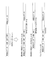
図1は、従来のSKIPオーダーセットを示す図である。
図1において、受信側が受信するデータのうち、SKIPオーダーセットは、有効なデータの間に挿入されている。
図1において、受信側が受信するデータのうち、SKIPオーダーセットは、有効なデータの間に挿入されている。
図1において、SKIPオーダーセットは、COMシンボルと2つのSKPシンボルから構成されている。図1のSKIPオーダーセットでは、COMシンボルの直後に2つのSKPシンボルが配置されている。
COMシンボルは、SKIPオーダーセットの先頭に配置されるシンボルである。
SKPシンボルは、受信側において追加または削除により、周波数差の調整に用いられるシンボルである。
SKPシンボルは、受信側において追加または削除により、周波数差の調整に用いられるシンボルである。
受信側LSIにおいて、データ受信回路は受信データのペースのクロック(以降、受信クロック)で動作し、SKIPオーダーセットを検出したら、吸収符号(SKPシンボル)を伸縮(追加または削除)することで、自分のクロック(以降、内部クロック)に転送レートを合わせる。
図2Aは、従来のSKIPオーダーセットを用いた周波数差の調整処理を示す図である。
図2Aの一番上のデータは、図1と同様の受信側が受信するデータを示す。図1で述べたように、有効なデータの間にSKIPオーダーセット(COMシンボルと2つのSKPシンボル)が挿入されている。
受信クロックから内部クロックへの乗換えにおいて、相対的に受信データが速い場合(すなわち、受信クロックが内部クロックより早い場合)、図2Aの上から2番目のデータに示すように、SKIPオーダーセットにさらにSKPシンボルを追加して、後段の回路へ渡すタイミングを遅くする。
相対的に受信データが遅い場合(すなわち、受信クロックが内部クロックより遅い場合)、図2Aの上から3番目のデータに示すように、SKIPオーダーセットからSKPシンボルを削除して、後段の回路へ渡すタイミングを速くする。
ちょうど良い場合(すなわち、受信クロックが内部クロックとほぼ同じ場合)、図2Aの上から4番目のデータに示すように、SKIPオーダーセットはそのままとする。
送信部は、データパケットにSKIPオーダーセットを挿入して、受信部に送信し、受信部は、周波数差を吸収するようにSKPキャラクタを挿入又は削除する技術が知られている(例えば、特許文献1参照)。
従来、SKIPオーダーセットを検出して、受信クロックと内部クロックとのタイミング誤差に基づいて、SKIPオーダーセット内のSKPシンボルの追加削除を行っている。その場合、先頭のCOMシンボルから最後尾のSKPシンボルまでを含むSKIPオーダーセットは、SKPシンボルの追加削除を行うまで、SKPシンボルの追加削除を行う処理回路近辺に滞留させておく必要があり、転送遅延の原因となる。
1つの側面において、本発明の課題は、回路内の周波数差を調整するための転送遅延(レイテンシ)を小さくすることである。
実施の形態の受信回路は、検出部と、判定部と、符号長制御部と、を有する。
前記検出部は、受信データから周波数差調整符号列の開始を表す開始符号を検出する。
前記判定部は、受信クロックと内部クロックとの間のタイミング誤差を判定する。
前記検出部は、受信データから周波数差調整符号列の開始を表す開始符号を検出する。
前記判定部は、受信クロックと内部クロックとの間のタイミング誤差を判定する。
符号長制御部は、前記判定部により判定されるタイミング誤差に応じて、前記受信データ中の前記開始符号が検出された位置から指定された距離だけ離れた位置に挿入されている調整符号の長さを調整する。
実施の形態の受信回路によれば、回路内の転送遅延を小さくすることができる。
LSI内の遅延を小さくするため、LSI内のさまざまな処理はパイプライン化を行うのが一般的である。
すなわち、ある処理が済んだデータは次段へ、その次の処理が済んだデータはさらに次段へと、LSI内でデータを遅滞なくスムーズに転送させてゆくことで、LSI内の転送遅延を小さくすることができる。
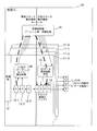
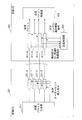
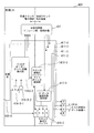
図2Bは、受信LSIの構成と処理の一例を示す図である。
受信LSI10は、受信レーン処理部11-k(k=0~3)および受信制御部21を備える。
受信LSI10は、受信レーン処理部11-k(k=0~3)および受信制御部21を備える。
受信LSI10は、送信LSI(不図示)と4本のレーンk(不図示)により接続されている。受信レーン処理部11-kは、レーンkを介して送信されたデータを受信して、該データに対して処理を行う。
図2Bでは、受信レーン処理部11-3の構成のみ詳細を記載している。受信レーン処理部11-0~11-2の構成は、受信レーン処理部11-3の構成と同様のため記載は省略する。
受信レーン処理部11-3は、受信部12、フリップフロップ13-1、13-2、13-3、SKIPオーダーセット検出部14、データ追加削除処理部15、およびクロック乗り換えバッファ16を備える。
受信部12は、送信LSIからデータを受信し、データをシリアルパラレル変換等の処理を施して、フリップフロップ13-1に出力する。
フリップフロップ13-1、13-2、13-3は、入力されたデータを保持し、受信クロックと同期して該データを出力する。ここで、データは1シンボル分のデータとする。
フリップフロップ13-1は、データをSKIPオーダーセット検出部14とフリップフロップ13-2に出力する。フリップフロップ13-2は、データをSKIPオーダーセット検出部14とフリップフロップ13-3に出力する。フリップフロップ13-3は、データをクロック乗換えバッファ16に出力する。
SKIPオーダーセット検出部14は、フリップフロップ13-1、13-2から入力されるデータをチェックし、SKIPオーダーセットを検出する。SKIPオーダーセット検出部14は、SKIPオーダーセットを検出すると、受信制御部21にSKIPオーダーセットの検出の通知をする。
受信部12、フリップフロップ13-1、13-2、13-3、およびSKIPオーダーセット検出部14は、受信クロックと同期して動作する。
データ追加削除処理部15は、受信制御部21の指示に基づいて、SKPシンボルの追加または削除を行う。詳細には、例えば、データ追加削除処理部15は、受信制御部の指示に基づいて、クロック乗換えバッファ16のリードポインタを調整する。
受信制御部21は、各受信レーン処理部11-kのSKIPオーダーセット検出部14から通知を受信し、各受信レーン処理部11-kのデータ追加削除処理部15にSKPシンボルの追加または削除の指示をする。
背景技術で述べた周波数差吸収動作は、(1)「SKIPオーダーセットを検出する」と(2)「検出の結果、必要に応じSKPシンボルを追加または削除する」の2つのフェーズから成っており、受信したデータの流れ(stream)のうちの、同じ箇所(SKIPオーダーセットの箇所)に対し、これを順番に実行せねばならない。(1)の処理はSKIPオーダーセット検出部14、(2)の処理はデータ追加削除処理部15によりそれぞれ行われる。
さらに、LSI間の伝送においては、複数のシリアル伝送(レーン)を束ねて、ある幅をもった単位にし、LSI内部(受信部より先)ではその単位でデータを取り扱う場合が多い。
一単位である複数のレーンの間で、SKPシンボルの処理時にレーン間の束ねがズレないようにするためには、受信レーン処理部11-kに同時に送られてくるSKIPオーダーセットに対し、符号の追加・削除を、受信レーン処理部11-k間で同期して判断する必要がある。
そのため、複数レーンを束ねてデータ転送をおこなう場合は、(1)と(2)のフェーズの間に、(1')受信制御部21において全受信レーン処理部11-kで判断を同期するフェーズを入れる必要がある。
データストリーム中の同じ箇所に対し、(1)→(1')→(2)の順番で処理を行うため、該箇所のデータは、(2)の処理が終わるまで、それらの処理をおこなう回路近辺(フリップフロップ13、クロック乗換えバッファ16)に滞留させておく必要がある。
これは、LSI内でのスムーズなデータの転送(処理のパイプライン化)を妨げ、転送遅延(レイテンシ)を大きくする要因になっている。
以下、図面を参照しながら実施の形態について説明する。
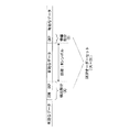
図3は、実施の形態に係るSKIPオーダーセットを示す図である。
図3は、実施の形態に係るSKIPオーダーセットを示す図である。
実施の形態のSKIPオーダーセットは、検出部分(A)と伸縮部分(B)から構成される。SKIPオーダーセットは、周波数差調整符号列の一例である。
検出部分(A)は、1つのCOMシンボルと1つのSKPシンボルで構成されている。検出部分(A)は、COMシンボルの直後にSKPシンボルが配置されている。検出部分は、開始符号の一例である。
伸縮部分(B)は、1つのSKPシンボルで構成されている。伸縮部分(B)は、調整符号の一例である。
検出部分(A)と伸縮部分(B)は、距離N(シンボル数)だけ離れて配置されている。距離Nは、固定シンボル長としても良いし、検出部分に含まれる予め定義したシンボルに応じて特定しても良いし、検出部分(A)と伸縮部分(B)との間のデータから取得したパケット長の情報から算出しても良い。
検出部分(A)と伸縮部分(B)の間には有効なデータ(ペイロード)または無効データが挿入される。
図4は、実施の形態に係るシステムの構成図である。
システム101は、情報処理装置201-i(i=1、2)を備える。
システム101は、情報処理装置201-i(i=1、2)を備える。
情報処理装置201-iは、Central Processing Unit(CPU)202-i-j(j-1、2)、クロスバースイッチ(XB)203-i、およびI/Oアダプタ204-i-k(k=0~3)を備える。
CPU202-i-1とCPU202-i-2は、複数のレーン(シリアルバス)により接続している。CPU202-i-jとXB203-iは、複数のレーンシリアルバス)により接続している。XB203-1とXB203-2は、複数のレーン(シリアルバス)により接続している。
CPU202-i-jは、各種処理を行う処理装置である。
XB203-iは、データの経路を動的に選択するスイッチである。XB203-iは、XB203-iまたはCPU202-i-jからパケットを受信し、そのパケットに含まれる宛先を認識し、送信先に転送する。
XB203-iは、データの経路を動的に選択するスイッチである。XB203-iは、XB203-iまたはCPU202-i-jからパケットを受信し、そのパケットに含まれる宛先を認識し、送信先に転送する。
I/Oアダプタ204-i-m(m=1~4)は、入出力装置と接続するアダプタである。
後述の実施の形態に係る送信LSIおよび受信LSIは、CPU202-i-jおよびXB203-iに搭載され、CPU-CPU間、CPU-XB間、およびXB-XB間の通信で使用される。
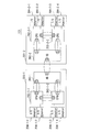
図5は、実施の形態に係る送信LSIおよび受信LSIの構成図である。
送信LSI301は、送信パケット生成部311および送信レーン処理部321-k(k=0~3)を備える。
送信LSI301は、送信パケット生成部311および送信レーン処理部321-k(k=0~3)を備える。
受信LSI401は、受信レーン処理部411-k、受信制御部421、および受信パケット解析部431を備える。
送信LSI301は、受信LSI401と4本のレーン(シリアルバス)で接続されている。送信レーン処理部321-kは、受信レーン処理部411-kとレーンを介して接続されている。以下、送信レーン処理部321-kと受信レーン処理部411-kとを接続するレーンをレーンkと表記する。
送信パケット生成部311は、受信LSIに送信する送信パケットを生成し、送信レーン処理部321-kに送信パケットを分割して送信する。
送信レーン処理部321-kは、SKIPオーダーセットを生成し、入力されたパケットにSKIPオーダーセットを挿入し、受信レーン処理部411-kに送信する。尚、送信レーン処理部321-kの詳細については後述する。
受信レーン処理部411-kは、入力されたデータからSKIPオーダーセットの検出部分と距離Nを検出し、受信制御部421に通知する。受信レーン処理部411-kは、受信制御部421から指示に基づいて、SKIPオーダーセットの伸縮部分(SKPシンボル)の追加または削除を行う。尚、受信レーン処理部411-kの詳細については後述する。受信レーン処理部411-kは、受信パケットを受信パケット解析部431に出力する。
受信制御部421は、受信クロックと内部クロックとの誤差、すなわち受信クロックと内部クロックとの周波数差を判定する。受信制御部421は、判定した誤差と受信レーン処理部411-kの通知に基づいて、受信レーン処理部411-kに伸縮部分の追加または削除の指示を行う。受信制御部421は、符号長制御部の一例である。尚、受信クロックは、受信データをクロックデータリカバリすることにより生成される。また、内部クロックは、受信LSI401内のクロック生成回路(不図示)により生成される。
受信パケット解析部431は、送信レーン処理部411-kから入力されたパケットに対して解析などの処理をする。受信パケット解析部431は、データ処理部の一例である。
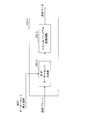
図6は、実施の形態に係る送信レーン処理部の構成図である。
送信レーン処理部321-kは、SKIPオーダーセット生成部322-kおよびパラレル/シリアル変換回路323-kを備える。
送信レーン処理部321-kは、SKIPオーダーセット生成部322-kおよびパラレル/シリアル変換回路323-kを備える。
SKIPオーダーセット生成部322-kは、例えば図3に示すSKIPオーダーセットを生成し、入力されたパケットの間にSKIPオーダーセットを挿入し、パラレル/シリアル変換回路323-kに出力する。
パラレル/シリアル変換回路323-kは、パラレルデータとシリアルデータを相互に変換する。パラレル/シリアル変換回路323-kは、入力されたパラレルデータをシリアルデータに変換し、レーンkを介して受信レーン処理部411-kに出力する。
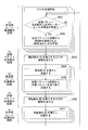
図7は、実施の形態に係る受信レーン処理部の構成図である。
受信レーン処理部411-kは、パラレル/シリアル変換回路412-k、SKIPオーダーセット検出部413-k、およびクロック乗り換えバッファ414-kを備える。
受信レーン処理部411-kは、パラレル/シリアル変換回路412-k、SKIPオーダーセット検出部413-k、およびクロック乗り換えバッファ414-kを備える。
パラレル/シリアル変換回路412-kは、パラレルデータとシリアルデータを相互に変換する。パラレル/シリアル変換回路412-kは、入力されたシリアルデータをパラレルデータに変換し、SKIPオーダーセット検出部413-kおよびクロック乗り換えバッファ414-kに出力する。
SKIPオーダーセット検出部413-kは、SKIPオーダーセットの検出部分と距離Nを検出し、受信制御部421に通知する。
クロック乗り換えバッファ414-kは、受信クロックから内部クロックへの乗り換えに用いるバッファである。すなわち、クロック乗り換えバッファ414-kは、受信クロックによりデータを書き込み、内部クロックによりデータを読み出す。クロック乗り換えバッファ414-kは、SKPシンボルの追加または削除により、周波数差の調整を行うためのバッファである。
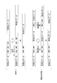
図8は、実施の形態に係る送信処理のフローチャートである。
ステップS501、S502、S504、S505、およびS507は、各送信レーン処理部321-kにおいて、それぞれ実行される。
ステップS501、S502、S504、S505、およびS507は、各送信レーン処理部321-kにおいて、それぞれ実行される。
ステップS501において、送信レーン処理部321-kは、送信パケット生成部311からSKIPオーダーセット送信指示を受信したか判定し、受信した場合、制御はステップS502に進む。受信していない場合、SKIPオーダーセット送信指示を受信するまで待機する。
ステップS502において、送信レーン処理部321-kは、送信パケット生成部311から距離Nの通知を受信する。尚、距離Nが固定シンボル長の場合、すなわち、距離Nが予め決まっている場合、ステップ502の処理は、無くても良い。
ステップS503において、送信パケット生成部311は、検出部分を挿入するだけの隙間をあける。
ステップS504において、送信レーン処理部321-kは、入力されたパケットに検出部分を挿入し、受信レーン処理部411-kに送信する。
ステップS505において、送信レーン処理部321-kは、送信パケット生成部311から充填パケット(すなわち、有効なデータ)を受信し、受信レーン処理部411-kに送信する。
ステップS506において、送信パケット生成部311は、伸縮部分を挿入するだけの隙間をあける。
ステップS507において、送信レーン処理部321-kは、入力されたパケットに伸縮部分を挿入し、受信レーン処理部411-kに送信する。
図9は、実施の形態に係る受信処理のフローチャートである。
ステップS601~S603、S606、およびS607は、各受信レーン処理部411-kにおいて、それぞれ実行される。
ステップS601~S603、S606、およびS607は、各受信レーン処理部411-kにおいて、それぞれ実行される。
ステップS601において、SKIPオーダーセット検出部413-kは、入力されたデータをチェックし、検出部分(A)を検出した場合、制御はステップS602に進む。
ステップS602において、SKIPオーダーセット検出部413-kは、距離Nを特定する。SKIPオーダーセット検出部413-kは、例えば、検出部分(A)の種類や検出部分(A)と伸縮部分(B)の間のデータから距離Nを特定する。尚、距離Nが固定シンボル長の場合、すなわち、距離Nが予め決まっている場合、ステップ602の処理は、無くても良い。
ステップS603において、SKIPオーダーセット検出部413-kは、検出部分(A)の検出と距離Nを受信制御部421に通知する。
ステップS604において、受信制御部421は、レーン間の同期待ちをする。すなわち、受信制御部421は、すべてのSKIPオーダーセット検出部413-kからの通知を待ち、すべてのSKIPオーダーセット検出部413-kから通知を受信したら、制御はステップS605に進む。送信LSI301と受信LSI401間の伝送においては、複数のレーンを束ねて、ある幅をもった単位にし、受信LSI301内部(受信レーン処理部411-kより後)ではその単位でデータを取り扱う場合が多い。一単位である複数のレーンの間で、SKPシンボルの処理時にレーン間の束ねがズレないようにするために、ステップS604においてレーン間の同期待ちを行っている。尚、レーン間の同期が不要の場合、ステップS604は省略しても良い。
ステップS605において、受信制御部421は、受信クロックと内部クロックとのタイミング誤差(受信クロックと内部クロックとの周波数差)を判定し、判定結果に基づいて、各受信レーン処理部411-kに伸縮部分(B)のSKPシンボルの追加または削除の指示をする。受信制御部421は、各受信レーン処理部411-kに距離Nを通知する。尚、距離Nが固定シンボル長の場合、受信制御部421は、距離Nを通知をしなくてもよい。
ステップS606において、受信レーン処理部411-kは、検出部分(A)から距離N後に受信する伸縮部分(B)に対して、SKPシンボルの追加または削除を行うためのタイミングの調整を行う。
ステップS607において、受信レーン処理部411-kは、伸縮部分(B)に対して、SKPシンボルの追加または削除を行う。
図10は、実施の形態に係る受信LSIの構成と処理を示す図である。
図10では、受信レーン処理部411-3の構成のみ詳細を記載している。受信レーン処理部411-0~411-2の構成は、受信レーン処理部411-3の構成と同様のため記載は省略する。
図10では、受信レーン処理部411-3の構成のみ詳細を記載している。受信レーン処理部411-0~411-2の構成は、受信レーン処理部411-3の構成と同様のため記載は省略する。
受信レーン処理部411-3は、受信部415-3、フリップフロップ416-3-1、416-3-2、SKIPオーダーセット検出部413-3、データ追加削除処理部417-3、およびクロック乗り換えバッファ414-3を備える。
受信部415-3は、送信LSI301からデータを受信し、データにシリアルパラレル変換等の処理を施して、フリップフロップ416-3-1とクロック乗換えバッファ414-3に出力する。また、受信部415-3は、クロックデータリカバリにより受信データから受信クロックを生成する。受信部415-3は、図7のシリアル/パラレル変換回路412-3を含む。
フリップフロップ416-3-1、416-3-2は、入力されたデータを保持し、受信クロックと同期して該データを出力する。ここで、データは1シンボル分のデータとする。
フリップフロップ416-3-1は、データをSKIPオーダーセット検出部413-3とフリップフロップ416-3-2に出力する。フリップフロップ416-3-2は、データをSKIPオーダーセット検出部413-3に出力する。
SKIPオーダーセット検出部413-3は、フリップフロップ416-3-1、416-3-2から入力されるデータをチェックし、SKIPオーダーセットの検出部分を検出する。例えば、SKIPオーダーセット検出部413-3は、フリップフロップ416-3-1からの入力がSKPシンボル、且つフリップフロップ416-3-2からの入力がCOMシンボルの場合、検出部分(A)を検出する。SKIPオーダーセット検出部413-3は、検出部分(A)を検出すると、受信制御部421に検出部分(A)の検出の通知をする。SKIPオーダーセット検出部413-3は、距離Nを特定して、受信制御部421に通知しても良い。
受信部415-3、フリップフロップ416-3-1、416-3-2、およびSKIPオーダーセット検出部413-3は、受信クロックと同期して動作する。
データ追加削除処理部417-3は、受信制御部421の指示に基づいて、伸縮部分(B)のSKPシンボルの追加または削除を行う。詳細には、例えば、データ追加削除処理部417-3は、受信制御部の指示に基づいて、クロック乗換えバッファ414-3のリードポインタを調整する。
クロック乗り換えバッファ414-3は、受信クロックと同期してデータを書き込み、内部クロックと同期してデータが読み出され、読み出されたデータは後段の受信パケット解析部431に渡される。
実施の形態のSKIPオーダーセットのように、符号列の方式を変えても、伸縮処理において、従来と同様に上述の(1)→(1')→(2)の処理を行う必要がある。実施の形態の受信処理では、SKPシンボルの伸縮の処理を行うときには、すでに検出部分(A)は必要なく、伸縮回路(クロック乗り換えバッファ414)の近辺を、伸縮対象の伸縮部分(B)が通過していればよい。
検出部分(A)については、SKIPオーダーセットであることを検出したあとは用いないので破棄してよく、すみやかなデータ転送(パイプライン化)の妨げとならない。SKPシンボルの伸縮の処理が終了する前に、検出部分(A)と伸縮部分(B)との間のデータの少なくとも一部は、後段の受信パケット解析部431に送られて処理され、すみやかなデータ転送が可能となる。
検出部分(A)と伸縮部分(B)との間の距離Nは、(1)→(1')→(2)の処理をおこなっている間に該当箇所を通過するシンボル数を上回る数とすることで、処理のパイプライン化の妨げとならないようにできる。
図11は、従来のSKIPオーダーセットと実施の形態に係るSKIPオーダーセットの周波数差の調整処理を示す図である。
図11の上半分は、従来のSKIPオーダーセットを用いた周波数差の調整処理を示し、図11の下半分は、実施の形態のSKIPオーダーセットを用いた周波数差の調整処理を示す。
図11の一番上のデータは、図1と同様の従来の受信側が受信するデータを示す。図1で述べたように、有効なデータの間にSKIPオーダーセット(COMシンボルと2つのSKPシンボル)が挿入されている。
図11の上半分の上から2番目と3番目のデータは、それぞれ受信クロックから内部クロックへの乗換えにおいて、相対的に受信データが速い場合と相対的に受信データが遅い場合のデータを示す。
図2Aで述べたように、相対的に受信データが速い場合は、SKPシンボルが追加され、相対的に受信データが遅い場合は、SKPシンボルは追加される。
図11の下半分のうち、一番上データは、図3と同様の実施の形態の受信側が受信するデータを示す。
実施の形態のSKIPオーダーセットは、検出部分(1つのCOMシンボルと1つのSKPシンボル)と伸縮部分(1つのSKPシンボル)から構成される。伸縮部分は、伸縮部分と距離N離れて配置されている。検出部分と伸縮部分の間には有効なデータ(ペイロード)が挿入されている。
図11の下半分のうち、上から2番目と3番目のデータは、それぞれ受信クロックから内部クロックへの乗換えにおいて、相対的に受信データが速い場合と相対的に受信データが遅い場合のデータを示す。
実施の形態において、相対的に受信データが速い場合は、伸縮部分にSKPシンボルが追加され、相対的に受信データが遅い場合は、伸縮部分にSKPシンボルが追加される。
実施の形態の受信LSIによれば、回路内の転送遅延を小さくすることができる。
実施の形態の受信LSIによれば、回路内の転送遅延を小さくすることができる。
(第1の変形例)
次に、SKIPオーダーセットの検出部分と伸縮部分との間の距離N(シンボル数)が可変シンボル長であり、距離Nを示す情報をSKIPオーダーセットに含める第1の変形例を説明する。
次に、SKIPオーダーセットの検出部分と伸縮部分との間の距離N(シンボル数)が可変シンボル長であり、距離Nを示す情報をSKIPオーダーセットに含める第1の変形例を説明する。
図12Aは、第1の変形例の距離N=6の場合のSKIPオーダーセットを示す図である。図12Aでは、上から順にレーン0からレーン3でそれぞれ送信される送信データを示している。
距離N=6の場合、検出部分は、COMシンボルとSKP-Aシンボルで構成する。検出部分と伸縮部分の間の距離は6である。検出部分と伸縮部分の間には、有効なデータが挿入されている。
図12Bは、第1の変形例の距離N=8の場合のSKIPオーダーセットを示す図である。図12Bでは、上から順にレーン0からレーン3でそれぞれ送信される送信データを示している。
距離N=8の場合、検出部分は、COMシンボルとSKP-Bシンボルで構成する。検出部分と伸縮部分の間の距離は8である。検出部分と伸縮部分の間には、有効なデータが挿入されている。
図12Cは、第1の変形例の距離N=10の場合のSKIPオーダーセットを示す図である。図12Cでは、上から順にレーン0からレーン3でそれぞれ送信される送信データを示している。
距離N=10の場合、検出部分は、COMシンボルとSKP-Cシンボルで構成する。検出部分と伸縮部分の間の距離は10である。検出部分と伸縮部分の間には、有効なデータが挿入されている。
図12Dは、第1の変形例の距離N=12の場合のSKIPオーダーセットを示す図である。図12Dでは、上から順にレーン0からレーン3でそれぞれ送信される送信データを示している。
距離N=12の場合、検出部分は、COMシンボルとSKP-Dシンボルで構成する。検出部分と伸縮部分の間の距離は12である。検出部分と伸縮部分の間には、有効なデータが挿入されている。
送信LSI301および受信LSI401において、上記のような距離に対応する検出部分の構成は、予め定義しておく。
送信LSI301および受信LSI401において、SKP-Aシンボル、SKP-Bシンボル、SKP-Cシンボル、およびSKP-Dシンボルをどのようなデータとするか予め定義しておく。
SKP-Aシンボル、SKP-Bシンボル、SKP-Cシンボル、およびSKP-Dシンボルは、他のシンボルと識別可能であれば、任意のデータでよい。
ここで、第1の変形例の送信側のSKIPオーダーセット挿入時の処理を説明する。
(a)送信パケット生成部311は、送信レーン処理部321-kのSKIPオーダーセット生成部322-kへ、SKIPオーダーセット挿入指示および距離Nを通知する。
(b)送信パケット生成部311は、検出部分(A)が挿入できるだけの隙間をつくる。送信レーン処理部321-kのSKIPオーダーセット生成部322-kは、その隙間に、距離Nに対応した検出部分(A)を挿入し、受信LSI401へ送信する。
(c)送信パケット生成部311は、検出部分(A)と伸縮部分(B)に充填するパケットを送信レーン処理部321-kに送信したのち、伸縮部分(B)を挿入するだけの隙間をつくる。SKIPオーダーセット生成部322-kは充填パケットを送信したのち、隙間に伸縮部分(B)を挿入して送信する。
図13は、第1の変形例の受信LSIの構成図である。
図13では、受信レーン処理部411-3の構成のみ詳細を記載している。受信レーン処理部411-0~411-2の構成は、受信レーン処理部411-3の構成と同様のため記載は省略する。
図13では、受信レーン処理部411-3の構成のみ詳細を記載している。受信レーン処理部411-0~411-2の構成は、受信レーン処理部411-3の構成と同様のため記載は省略する。
受信レーン処理部411-3は、受信部415-3、フリップフロップ416-3-1、416-3-2、SKIPオーダーセット/距離検出部1413-3、データ追加削除処理部417-3、クロック乗換えバッファライトポインタ通知部1418-3、およびクロック乗り換えバッファ414-3を備える。
受信部415-3、フリップフロップ416-3-1、416-3-2、データ追加削除処理部417-3、およびクロック乗り換えバッファ414-3は、図10と機能を有するため説明は省略する。
SKIPオーダーセット/距離検出部1413-3は、フリップフロップ416-3-1、416-3-2から入力されるデータをチェックし、SKIPオーダーセットの検出部分と距離N検出する。例えば、SKIPオーダーセット検出部413-3は、フリップフロップ416-3-1からの入力がSKPシンボル、且つフリップフロップ416-3-2からの入力がCOM-Aシンボルの場合、検出部分と距離N=6検出する。SKIPオーダーセット検出部413-3は、検出部分を検出すると、受信制御部421に検出部分の検出と距離Nを通知する。
クロック乗換えバッファライトポインタ通知部1418-3は、検出部分の検出時のクロック乗換えバッファ414-3のライトポインタ値をクロック乗換えバッファ側に通知する。
第1の変形例の受信LSI401のSKIPオーダーセット受信時の処理は、以下のようになる。
(1)各受信レーン処理部411-kのSKIPオーダーセット/距離検出部1413は、受信した検出部分(A)から、SKIPオーダーセット検出および距離Nを検出する。検出した情報を、受信制御部421に通知する。また、SKIPオーダーセット検出時のクロック乗換えバッファのライトポインタ値を受信クロックから内部クロックに乗換え、読出し側に通知する。
(1’)受信制御部421は、通知されたSKIPオーダーセットおよび距離Nを、受信クロックから内部クロックへ乗換える。受信制御部421は、各受信レーン処理部411-kから通知された情報が異なっていた場合は、多数決にて決定する(レーン間の同期判断)。受信制御部421は、各受信レーン処理部411-kに符号(SKPシンボル)の追加または削除を指示する。また、受信制御部421は距離Nを通知する。
(2)クロック乗換えバッファ414-kは、受信制御部421から通知された距離Nと書き込み側から通知されたクロック乗換えバッファのライトポインタ値により、検出部分(A)から距離N後に受信した伸縮部分(B)のクロック乗換えバッファ内位置を特定する。そして、データ追加削除処理部417-3は、受信制御部421からの指示により伸縮部分(B)に対してSKPシンボルの追加・削除を行う。
この(1)→(1’)→(2)の処理の間において、検出部分(A)と伸縮部分(B)の間に充填されたパケットは、各受信レーン処理部411-kで受信後、すみやかに後段のパケット解析部431に受け渡される。
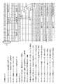
図14A、14Bは、第1の変形例のSKIPオーダーセット受信時のタイムチャートである。
図14A、14Bの各チャートは上から順に下記の通りである。
(1)受信クロック。SKIPオーダーセット検出回路に有効データ1の先頭が到達したときをt0とする。
(2)SKIPオーダーセット検出回路内の受信データ。受信データは、(i)有効データ1 (6シンボル長)、(ii)SKIPオーダーセットの検出部分(A)、(iii)有効データ2(充填パケット)(6シンボル長)、(iv)SKIPオーダーセットの伸縮部分(B)、(v)有効データ3 (6シンボル長)の順に構成されたデータである。以降、有効データ4、5と続く。
(3)SKIPオーダーセット検出部分(A)検出・距離N検出のタイミング
(4)クロック乗換えバッファのライトポインタ値
(5)クロック乗換えバッファへの書込みデータ
(6)内部クロック。受信クロックがt0のとき、内部クロックをT0とする。
(7)検出部分(A)検出通知・距離N通知の、受信クロックから内部クロックへの乗換えタイミング
(8)検出部分(A)検出・距離N・符号追加削除のレーン間同期
(9)受信レーン処理部に通知された符号追加削除指示と距離N
(10)検出部分(A)の検出時におけるライトポインタ値の、受信クロックから内部クロックへの乗換え。
(11)クロック乗換バッファ読出し側に通知された、検出部分(A)検出時のライトポインタ値。
(12)伸縮部分(B)のクロック乗換えバッファライトポインタ値((11)のライトポインタ値と(9)の距離Nからの算出値)
(13)クロック乗換えバッファ内のリードポインタ値(追加削除しない場合)
(14)クロック乗換えバッファからの読出しデータ(追加削除しない場合)
(15)クロック乗換えバッファ内のリードポインタ値 (追加する場合)
(16)クロック乗換えバッファからの読出しデータ(追加する場合)
(17)クロック乗換えバッファ内のリードポインタ値(削除する場合)
(18)クロック乗換えバッファからの読出しデータ(削除する場合)
(1)受信クロック。SKIPオーダーセット検出回路に有効データ1の先頭が到達したときをt0とする。
(2)SKIPオーダーセット検出回路内の受信データ。受信データは、(i)有効データ1 (6シンボル長)、(ii)SKIPオーダーセットの検出部分(A)、(iii)有効データ2(充填パケット)(6シンボル長)、(iv)SKIPオーダーセットの伸縮部分(B)、(v)有効データ3 (6シンボル長)の順に構成されたデータである。以降、有効データ4、5と続く。
(3)SKIPオーダーセット検出部分(A)検出・距離N検出のタイミング
(4)クロック乗換えバッファのライトポインタ値
(5)クロック乗換えバッファへの書込みデータ
(6)内部クロック。受信クロックがt0のとき、内部クロックをT0とする。
(7)検出部分(A)検出通知・距離N通知の、受信クロックから内部クロックへの乗換えタイミング
(8)検出部分(A)検出・距離N・符号追加削除のレーン間同期
(9)受信レーン処理部に通知された符号追加削除指示と距離N
(10)検出部分(A)の検出時におけるライトポインタ値の、受信クロックから内部クロックへの乗換え。
(11)クロック乗換バッファ読出し側に通知された、検出部分(A)検出時のライトポインタ値。
(12)伸縮部分(B)のクロック乗換えバッファライトポインタ値((11)のライトポインタ値と(9)の距離Nからの算出値)
(13)クロック乗換えバッファ内のリードポインタ値(追加削除しない場合)
(14)クロック乗換えバッファからの読出しデータ(追加削除しない場合)
(15)クロック乗換えバッファ内のリードポインタ値 (追加する場合)
(16)クロック乗換えバッファからの読出しデータ(追加する場合)
(17)クロック乗換えバッファ内のリードポインタ値(削除する場合)
(18)クロック乗換えバッファからの読出しデータ(削除する場合)
図14A、14Bのタイムチャートの流れを以下で説明する。ここで、受信クロックから内部クロックへの乗換えのためのラッチは3段とする。
(ア)時刻t0において、有効データ1の先頭が、SKIPオーダーセット検出回路への到達し、クロック乗換えバッファへ書き込まれる。
(イ)時刻t7において、(2)より、SKIPオーダーセット検出回路でCOMおよびSKP-Aを検出する。したがって、(3)より、SKIPオーダーセット検出部分(A)の検出および距離Nの検出を行う。
(ウ)時刻T7-T9において、(7)より、(イ)のSKIPオーダーセット検出部分(A)検出・距離N検出の受信クロックから内部クロックへクロックを乗換える。
尚、受信クロックと内部クロックのタイミングによっては、時刻T8-T10となるケースもある。この場合は、以下(エ)~(カ)、(ク)の実行タイミングが変わり、内部クロックが+1となる。しかし、(14)、(16)(18)に示す読出しデータは変わらない。
(エ)時刻T10において、(8)より、(ウ)の結果を用いてSKIPオーダーセット検出・距離Nのレーン間同期を行う。
(オ)時刻T11において、(9)より、(エ)の結果を用いて、各受信レーン処理部411-kのデータ追加削除処理部417-3へ、符号追加削除指示および距離Nを通知する。通知された指示は、符号追加削除を実行するまで、各各受信レーン処理部411-kのデータ追加削除処理部417-3で保持しておく。
(カ)時刻T7-T9において、(10)より、(イ)の結果を用いて、SKIPオーダーセット検出部分(A)の検出時の(4)クロック乗換えバッファのライトポインタ値の、受信クロックから内部クロックへのクロック乗り換えを行う。
尚、受信クロックと内部クロックのタイミングによっては、時刻T8-T10となるケースもある。この場合は、以下(キ)の実行タイミングが変わり、内部クロックが+1となる。しかし、(14)、(16)(18)に示す読出しデータは変わらない。
(キ)時刻T10において、(11)より、(カ)の結果を用いて、検出部分(A)検出時のライトポインタ値(時刻t7の(4)の値)を、クロック乗換えバッファ側に通知する。
(ク)時刻T12において、(12)により、(オ)と(キ)の結果を用いて、「検出部分(A)検出時のライトポインタ値」と「距離N」から、伸縮部分(B)のライトポインタ値を算出する。
(ケ)時刻T15において、(12)と(13)により、クロック乗換えバッファのリードポインタが伸縮部分(B)の直前を指していることを検出し、(オ)の結果を用いて、以下の制御を行う。
(ケ-1) SKPシンボルの追加削除をしない場合
時刻T16でリードポインタ値を+1する。
これによりリードポインタ値は(13)、読み出しデータは(14)に示す通りになり、伸縮部分(B)が1度だけ読み出される。
(ケ-2) SKPシンボルを追加する場合
時刻T16でリードポインタ値を+1したのち、T17でホールドする。
これによりリードポインタ値は(15)、読み出しデータは(16)に示す通りになり、伸縮部分(B)が2度読み出される。
(ケー3)SKPシンボルを削除する場合
時刻T16でリードポインタ値を+2する。
これにより、伸縮部分(B)が読み飛ばされる。
(ケ-1) SKPシンボルの追加削除をしない場合
時刻T16でリードポインタ値を+1する。
これによりリードポインタ値は(13)、読み出しデータは(14)に示す通りになり、伸縮部分(B)が1度だけ読み出される。
(ケ-2) SKPシンボルを追加する場合
時刻T16でリードポインタ値を+1したのち、T17でホールドする。
これによりリードポインタ値は(15)、読み出しデータは(16)に示す通りになり、伸縮部分(B)が2度読み出される。
(ケー3)SKPシンボルを削除する場合
時刻T16でリードポインタ値を+2する。
これにより、伸縮部分(B)が読み飛ばされる。
以上の制御を行うため、有効データ1の先頭は時刻T2で、有効データ2の先頭は時刻t10で、有効データ3の先頭は時刻T17~T19で読み出すことができ、すみやかに後段のパケット解析部に受け渡される。
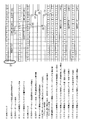
ここで、比較のために、従来のタイムチャートを図15A、15Bに示す。
図15A、15Bは、従来のSKIPオーダーセット受信時のタイムチャートである。
図15A、15Bは、従来のSKIPオーダーセット受信時のタイムチャートである。
図15A、15Bの各チャートは上から順に下記の通りである。
(1)受信クロック。SKIPオーダーセット検出回路に有効データ1の先頭が到達したときをt0とする。
(2)SKIPオーダーセット検出回路内の受信データ。
(3)SKIPオーダーセット検出のタイミング
(4)クロック乗換えバッファのライトポインタ値
(5)クロック乗換えバッファへの書込みデータ
(6)内部クロック。受信クロックがt0のとき、内部クロックをT0とする。
(7)SKIPオーダーセット検出通知の、受信クロックから内部クロックへの乗換えタイミング
(8)SKIPオーダーセット検出・符号追加削除のレーン間同期
(9)各レーンへ通知された符号追加削除指示
(10)SKIPオーダーセット検出時におけるライトポインタ値の、受信クロックから内部クロックへの乗換え。
(11)クロック乗換バッファ読出し側に通知されたSKIPオーダーセット検出時のライトポインタ値。
(12)伸縮部分のクロック乗換えバッファのライトポインタ値((11)のライトポインタ値と(9)の距離Nからの算出値)
(13)クロック乗換えバッファ内のリードポインタ値(追加削除しない場合)
(14)クロック乗換えバッファからの読出しデータ(追加削除しない場合)
(15)クロック乗換えバッファ内のリードポインタ値(追加する場合)
(16)クロック乗換えバッファからの読出しデータ(追加する場合)
(17)クロック乗換えバッファ内のリードポインタ値(削除する場合)
(18)クロック乗換えバッファからの読出しデータ(削除する場合)
(1)受信クロック。SKIPオーダーセット検出回路に有効データ1の先頭が到達したときをt0とする。
(2)SKIPオーダーセット検出回路内の受信データ。
(3)SKIPオーダーセット検出のタイミング
(4)クロック乗換えバッファのライトポインタ値
(5)クロック乗換えバッファへの書込みデータ
(6)内部クロック。受信クロックがt0のとき、内部クロックをT0とする。
(7)SKIPオーダーセット検出通知の、受信クロックから内部クロックへの乗換えタイミング
(8)SKIPオーダーセット検出・符号追加削除のレーン間同期
(9)各レーンへ通知された符号追加削除指示
(10)SKIPオーダーセット検出時におけるライトポインタ値の、受信クロックから内部クロックへの乗換え。
(11)クロック乗換バッファ読出し側に通知されたSKIPオーダーセット検出時のライトポインタ値。
(12)伸縮部分のクロック乗換えバッファのライトポインタ値((11)のライトポインタ値と(9)の距離Nからの算出値)
(13)クロック乗換えバッファ内のリードポインタ値(追加削除しない場合)
(14)クロック乗換えバッファからの読出しデータ(追加削除しない場合)
(15)クロック乗換えバッファ内のリードポインタ値(追加する場合)
(16)クロック乗換えバッファからの読出しデータ(追加する場合)
(17)クロック乗換えバッファ内のリードポインタ値(削除する場合)
(18)クロック乗換えバッファからの読出しデータ(削除する場合)
図15A、15Bのタイムチャートの流れを以下で説明する。尚、受信データは、上記の第1の変形例と同じとする。また、受信クロックから内部クロックへの乗換えのためのラッチも、上記の第1の変形例と同じとする。
(ア)時刻t0において、有効データ1の先頭が、SKIPオーダーセット検出回路へ到達する。
(イ)時刻t7において、(2)より、SKIPオーダーセット検出回路でCOMシンボルおよびSKPシンボルを検出する。したがって、(3)より、SKIPオーダーセット検出を行う。
(ウ)時刻T7-T9において、(7)より、(イ)のSKIPオーダーセット検出の受信クロックから内部クロックへクロック乗換えを行う。
受信クロックと内部クロックのタイミングによっては、クロック乗換えは時刻T8-T10となるケースもある。この場合は、以下(エ)~(カ)、(ク)の実行タイミングが変わり、内部クロックが+1となる。しかし、(14)、(16)、および(18に示す読出しデータは変わらない。
(エ)時刻T10において、(8)より、(ウ)の結果を用いてSKIPオーダーセット検出のレーン間同期を行う。
(オ)時刻T11において、(9)より、(エ)の結果を用いて、各受信レーン処理部411-kのデータ追加削除処理部417-3へ符号追加削除指示を通知する。通知された指示は、符号追加削除を実行するまで、各受信レーン処理部411-kのデータ追加削除処理部417-3で保持しておく。
(カ)時刻T7-T9において、(10)より、(イ)の結果を用いて、SKIPオーダーセット検出時の(4)クロック乗換えバッファのライトポインタ値の、受信クロックから内部クロックへの、クロック乗換えを行う。
受信クロックと内部クロックのタイミングによっては、時刻T8-T10となるケースもある。この場合は、以下(キ)の実行タイミングが変わり、内部クロックが+1となる。しかし、(14)、(16)、および(18)に示す読出しデータは変わらない。
(キ)時刻T10において、(11)より、(カ)の結果を用いて、SKIPオーダーセット検出時のライトポインタ値(t7の(4)の値)を、クロック乗換えバッファ側に通知する
(ク)時刻T10において、(12)により、(キ)の結果を用いて「SKIPオーダーセット検出時のライトポインタ値」から、SKIPオーダーセット伸縮部分のライトポインタ値を算出する。ここで、SKIPオーダーセット検出時のライトポインタ値とSKIPオーダーセット伸縮部分のライトポインタ値は一意に決まるため、定数を加算すればよい。
(ケ)時刻T14において、(12)と(13)により、クロック乗換えバッファのリードポインタ値が伸縮部分の直前を指していることを検出し、(オ)の結果を用いて、以下の制御を行う。
(ケ-1) 符号の追加削除をしない場合
時刻T15でリードポインタ値を+1する。
これによりリードポインタ値は(13)、読み出しデータは(14)に示す通りとなり、伸縮部分が1度だけ読み出される。
(ケ-2) 符号を追加する場合
時刻T15でリードポインタ値を+1したのち、T16でホールドする。
これによりリードポインタ値は(15)、読み出しデータは(16)に示す通りとなり、伸縮部分)が2度読み出される。
(ケー3) 符号を削除する場合、T15でリードポインタ値を+2する。
これにより、伸縮部分が読み飛ばされる。
(ケ-1) 符号の追加削除をしない場合
時刻T15でリードポインタ値を+1する。
これによりリードポインタ値は(13)、読み出しデータは(14)に示す通りとなり、伸縮部分が1度だけ読み出される。
(ケ-2) 符号を追加する場合
時刻T15でリードポインタ値を+1したのち、T16でホールドする。
これによりリードポインタ値は(15)、読み出しデータは(16)に示す通りとなり、伸縮部分)が2度読み出される。
(ケー3) 符号を削除する場合、T15でリードポインタ値を+2する。
これにより、伸縮部分が読み飛ばされる。
以上の制御により、有効データ1の先頭は時刻T6で、有効データ2の先頭は時刻T14~T16で、有効データ3の先頭は時刻T16~T18でクロック乗換えバッファから読み出されることになる。
(第2の変形例)
次に、SKIPオーダーセットの検出部分と伸縮部分との間の距離N(シンボル数)を検出部分と伸縮部分との間に挿入されているデータから判断する第2の変形例を説明する。
次に、SKIPオーダーセットの検出部分と伸縮部分との間の距離N(シンボル数)を検出部分と伸縮部分との間に挿入されているデータから判断する第2の変形例を説明する。
図16は、第2の変形例のSKIPオーダーセットを示す図である。
図16では、上から順にレーン0からレーン3でそれぞれ送信される送信データを示している。
図16では、上から順にレーン0からレーン3でそれぞれ送信される送信データを示している。
第2の変形例のSKIPオーダーセットは、検出部分と伸縮部分から構成される。
検出部分は、1つのCOMシンボルと1つのSKPシンボルで構成されている。検出部分は、COMシンボルの直後にSKPシンボルが配置されている。
検出部分は、1つのCOMシンボルと1つのSKPシンボルで構成されている。検出部分は、COMシンボルの直後にSKPシンボルが配置されている。
伸縮部分は、1つのSKPシンボルで構成されている。
検出部分と伸縮部分は、距離N(シンボル数)だけ離れて配置されている。検出部分と伸縮部分の間には有効なデータが挿入されている。
検出部分と伸縮部分は、距離N(シンボル数)だけ離れて配置されている。検出部分と伸縮部分の間には有効なデータが挿入されている。
4つのレーンを介して送信された検出部分と伸縮部分との間に充填されるデータは、単一のパケットとする。パケットは、例えばトランザクションレイヤパケット(TLP)である。送信LSIでは、単一のパケットを4つに分割して、分割したパケットをそれぞれ各レーンで送信される検出部分と伸縮部分との間に挿入する。
パケットは、パケット長(PKT長)が記述されたフィールド(パケットヘッダ)を有する。送信パケット生成部311は、パケット長が記述されたフィールドが特定のレーンで送信されるようにする。
図16において、パケット長は、レーン3を介して送信されるデータの検出部分と伸縮部分との間に挿入される。
ここで、第2の変形例の送信側のSKIPオーダーセット挿入時の処理を説明する。
(a)送信パケット生成部311は、送信レーン処理部321-kのSKIPオーダーセット生成部322-kへ、SKIPオーダーセット挿入指示および距離Nを通知する。
(b)送信パケット生成部311は、検出部分(A)が挿入できるだけの隙間をつくる。送信レーン処理部321-kのSKIPオーダーセット生成部322-kは、その隙間に、検出部分(A)を挿入し、受信LSI401へ送信する。
(c)送信パケット生成部311は、検出部分(A)と伸縮部分(B)に充填するパケットを送信レーン処理部321-kに送信したのち、伸縮部分(B)を挿入するだけの隙間をつくる。SKIPオーダーセット生成部322-kは充填パケットを送信したのち、隙間に伸縮部分(B)を挿入して送信する。
図17は、第2の変形例に係る受信LSIの構成図である。
図17では、受信レーン処理部411-3の構成のみ詳細を記載している。受信レーン処理部411-0~411-2の構成は、受信レーン処理部411-3の構成と同様のため記載は省略する。
図17では、受信レーン処理部411-3の構成のみ詳細を記載している。受信レーン処理部411-0~411-2の構成は、受信レーン処理部411-3の構成と同様のため記載は省略する。
受信レーン処理部411-3は、受信部415-3、フリップフロップ416-3-1、416-3-2、416-3-3、SKIPオーダーセット検出部413-3、データ追加削除処理部417-3、クロック乗換えバッファライトポインタ通知部1418-3、距離算出部1419-3、およびクロック乗り換えバッファ414-3を備える。
受信部415-3、フリップフロップ416-3-1、416-3-2、データ追加削除処理部417-3、クロック乗換えバッファライトポインタ通知部1418-3、およびクロック乗り換えバッファ414-3は、図10、13と機能を有するため説明は省略する。
フリップフロップ416-3-3は、入力されたデータを保持し、受信クロックと同期して該データを出力する。ここで、データは1シンボル分のデータとする。フリップフロップ416-3-2は、受信部415-3からのデータを距離算出部1419-3に出力する。
距離算出部1419-3は、検出部分と伸縮部分の間のあるデータ(パケットのヘッダ)からパケット長を取得し、距離Nを算出し、算出した距離Nを受信制御部421に通知する。距離算出部1419-3は、例えば、パケット長をレーン数で除算して、距離Nを算出する。尚、距離算出部は、受信レーン処理部411-0~411-2では無くても良い。
第2の変形例の受信LSI401のSKIPオーダーセット受信時の処理は、以下のようになる。
(1)各受信レーン処理部411-kのSKIPオーダーセット検出部413-kは、受信した検出部分(A)から、SKIPオーダーセットであることを検出し、受信制御部421に通知する。
(1’’)特定の受信レーン処理部(ここでは、受信レーン処理部411-3)の距離算出部1419-3において、後続の充填パケットからパケット長を取得し、算出した距離Nを受信制御部に通知する。
(1’)受信制御部421は、通知されたSKIPオーダーセットおよび距離Nを、受信クロックから内部クロックへ乗換える。受信制御部421は、各受信レーン処理部411-kから通知された情報が異なっていた場合は、多数決にて決定する(レーン間の同期判断)。受信制御部421は、各受信レーン処理部411-kに符号(SKPシンボル)の追加または削除を指示する。また、受信制御部421は距離Nを通知する。
(2)クロック乗換えバッファ414-kは、受信制御部421から通知された距離Nと書き込み側から通知されたクロック乗換えバッファのライトポインタ値により、検出部分(A)から距離N後に受信した伸縮部分(B)のクロック乗換えバッファ内位置を特定する。そして、データ追加削除処理部417-3は、受信制御部421からの指示により伸縮部分(B)に対してSKPシンボルの追加・削除を行う。
この(1)→(1’)→(2)の処理の間において、検出部分(A)と伸縮部分(B)の間に充填されたパケットは、各受信レーン処理部411-kで受信後、すみやかに後段のパケット解析部431に受け渡される。
ここで、送信側においてSKIPオーダーセット挿入時に検出部分(A)と伸縮部分(b)との間に充填すべきパケットがない場合、送信パケット生成部311は、有効なパケットと同様のパケットフォーマットである無効パケットを充填する。受信側は、有効パケット充填時と同様に、無効パケットのパケット長から距離Nを算出することで伸縮部分(B)に対して、SKIP符号の追加・削除を行う。無効パケットはパケット解析部431で破棄される。
また、送信側において、全レーンで追加・削除判断を同期するフェーズ(1')を行うために必要なシンボル時間に対して充填パケットが短い場合は、充填パケットと伸縮部分(B)の間に無効データ(以降、PAD)を挿入する。PADの挿入量は、PADと充填パケットの合計の長さが、フェーズ(1’)に必要なシンボル時間を満たす分だけである。伸縮部分(B)はPADのあとにSKIPオーダーセット生成部322-kにより挿入され、送信される。
PADを入れる必要のあるパケット長はあらかじめ決まるため、受信側は、パケット長を検出した際にPADを含めた距離Nを算出して、受信制御部421に通知する。これによりSKIPシンボルの追加削除指示のタイミングと伸縮部分(B)を受信するタイミングとが一致し、SKIPシンボルの追加削除を行う。
図18A、18Bは、第2の変形例のSKIPオーダーセット受信時のタイムチャートである。
図18A、18Bの各チャートは上から順に下記の通りである。
(1)受信クロック。SKIPオーダーセット検出回路に有効データ1の先頭が到達したときをt0とする。
(2)SKIPオーダーセット検出回路内の受信データ。受信データは、(i)有効データ1 (6シンボル長)、(ii)SKIPオーダーセットの検出部分(A)、(iii)有効データ2(充填パケット)(6シンボル長)、(iv)SKIPオーダーセットの伸縮部分(B)、(v)有効データ3 (6シンボル長)の順に構成されたデータである。以降、有効データ4、5と続く。
(3)SKIPオーダーセット検出部分(A)検出・距離N検出のタイミング
(4)クロック乗換えバッファのライトポインタ値
(5)クロック乗換えバッファへの書込みデータ
(6)内部クロック。受信クロックがt0のとき、内部クロックをT0とする。
(7)検出部分(A)検出通知・距離N通知の、受信クロックから内部クロックへの乗換えタイミング
(8)検出部分(A)検出・距離N・符号追加削除のレーン間同期
(9)受信レーン処理部に通知された符号追加削除指示と距離N
(10)検出部分(A)の検出時におけるライトポインタ値の、受信クロックから内部クロックへの乗換え。
(11)クロック乗換バッファ読出し側に通知された、検出部分(A)検出時のライトポインタ値。
(12)伸縮部分(B)のクロック乗換えバッファライトポインタ値((11)のライトポインタ値と(9)の距離Nからの算出値)
(13)クロック乗換えバッファ内のリードポインタ値(追加削除しない場合)
(14)クロック乗換えバッファからの読出しデータ(追加削除しない場合)
(15)クロック乗換えバッファ内のリードポインタ値 (追加する場合)
(16)クロック乗換えバッファからの読出しデータ(追加する場合)
(17)クロック乗換えバッファ内のリードポインタ値(削除する場合)
(18)クロック乗換えバッファからの読出しデータ(削除する場合)
(1)受信クロック。SKIPオーダーセット検出回路に有効データ1の先頭が到達したときをt0とする。
(2)SKIPオーダーセット検出回路内の受信データ。受信データは、(i)有効データ1 (6シンボル長)、(ii)SKIPオーダーセットの検出部分(A)、(iii)有効データ2(充填パケット)(6シンボル長)、(iv)SKIPオーダーセットの伸縮部分(B)、(v)有効データ3 (6シンボル長)の順に構成されたデータである。以降、有効データ4、5と続く。
(3)SKIPオーダーセット検出部分(A)検出・距離N検出のタイミング
(4)クロック乗換えバッファのライトポインタ値
(5)クロック乗換えバッファへの書込みデータ
(6)内部クロック。受信クロックがt0のとき、内部クロックをT0とする。
(7)検出部分(A)検出通知・距離N通知の、受信クロックから内部クロックへの乗換えタイミング
(8)検出部分(A)検出・距離N・符号追加削除のレーン間同期
(9)受信レーン処理部に通知された符号追加削除指示と距離N
(10)検出部分(A)の検出時におけるライトポインタ値の、受信クロックから内部クロックへの乗換え。
(11)クロック乗換バッファ読出し側に通知された、検出部分(A)検出時のライトポインタ値。
(12)伸縮部分(B)のクロック乗換えバッファライトポインタ値((11)のライトポインタ値と(9)の距離Nからの算出値)
(13)クロック乗換えバッファ内のリードポインタ値(追加削除しない場合)
(14)クロック乗換えバッファからの読出しデータ(追加削除しない場合)
(15)クロック乗換えバッファ内のリードポインタ値 (追加する場合)
(16)クロック乗換えバッファからの読出しデータ(追加する場合)
(17)クロック乗換えバッファ内のリードポインタ値(削除する場合)
(18)クロック乗換えバッファからの読出しデータ(削除する場合)
図18A、18Bのタイムチャートの流れを以下で説明する。尚、受信データは、上記の第1の変形例と同じとする。また、受信クロックから内部クロックへの乗換えのためのラッチも、上記の第1の変形例と同じとする。
(ア)時刻t0において、有効データ1の先頭が、SKIPオーダーセット検出回路への到達し、クロック乗換えバッファへ書き込まれる。
(イ)時刻t7において、(2)より、SKIPオーダーセット検出回路でCOMシンボルおよびSKPシンボルを検出する。したがって、(3)より、SKIPオーダーセット検出部分(A)の検出を行う。
(イ’)時刻t8において、(2)と(3)より、(イ)の検出部分(A)の検出の次のタイミングで、特定レーン、すなわち第2の変形例ではレーン#3において、有効データ2、すなわち充填パケットのPKT長を取得し距離Nを算出する。
(ウ)時刻T7-T9において、(7)より、(イ)のSKIPオーダーセット検出部分(A)検出の受信クロックから内部クロックへのクロック乗換えを行う。
受信クロックと内部クロックのタイミングによっては、時刻T8-T10となるケースもある。この場合は、以下(エ)~(カ)、(ク)の実行タイミングが変わり、内部クロックが+1となる。しかし、(14)、(16)、および(18)に示す読出しデータは変わらない。
受信クロックと内部クロックのタイミングによっては、時刻T8-T10となるケースもある。この場合は、以下(エ)~(カ)、(ク)の実行タイミングが変わり、内部クロックが+1となる。しかし、(14)、(16)、および(18)に示す読出しデータは変わらない。
(ウ’)時刻T8-T10において、(7’)より、(イ’)の距離N算出の受信クロックから内部クロックへクロック乗換えを行う。
受信クロックと内部クロックのタイミングによっては、時刻T9-T11となるケースもある。この場合は、以下(オ’)の実行タイミングが変わり、内部クロックが+1となる。しかし、(14)、(16)、(18)に示す読出しデータは変わらない。
(エ)時刻T10において、(8)より、(ウ)の結果を用いてSKIPオーダーセット検出のレーン間同期を行う。
(オ)時刻T11において、(エ)の結果を用いて、各受信レーン処理部411-kのデータ追加削除処理部417-3へ符号追加削除指示を通知する。通知された指示は、符号追加削除を実行するまで、各受信レーン処理部411-kのデータ追加削除処理部417-3で保持しておく。
(オ’)時刻T11において、(ウ’)の結果を用いて、各受信レーン処理部411-kのデータ追加削除処理部417-3へ距離Nを通知する。
(カ)時刻T7-T9において、(10)より、(イ)の結果を用いて、SKIPオーダーセット検出部分(A)の検出時の(4)クロック乗換えバッファのライトポインタ値の、受信クロックから内部クロックへのクロック乗り換えを行う。
尚、受信クロックと内部クロックのタイミングによっては、時刻T8-T10となるケースもある。この場合は、以下(キ)の実行タイミングが変わり、内部クロックが+1となる。しかし、(14)、(16)、および(18)に示す読出しデータは変わらない。
(キ)時刻T10において、(11)より、(カ)の結果を用いて、検出部分(A)検出時のライトポインタ値(時刻t7の(4)の値)を、クロック乗換えバッファ側に通知する。
(ク) T12において、(12)により、(オ’)と(キ)の結果を用いて、「検出部分(A)検出時のライトポインタ値」と「距離N」から、伸縮部分(B)のライトポインタ値を算出する。
(ケ)時刻T15において、(12)と(13)により、クロック乗換えバッファのリードポインタが伸縮部分(B)の直前を指していることを検出し、(オ)の結果を用いて、以下の制御を行う。
(ケ-1) SKPシンボルの追加削除をしない場合
時刻T16でリードポインタ値を+1する。
これによりリードポインタ値は(13)、読み出しデータは(14)に示す通りになり、伸縮部分(B)が1度だけ読み出される。
(ケ-2) SKPシンボルを追加する場合
時刻T16でリードポインタ値を+1したのち、T17でホールドする。
これによりリードポインタ値は(15)、読み出しデータは(16)に示す通りになり、伸縮部分(B)が2度読み出される。
(ケ-3)SKPシンボルを削除する場合
時刻T16でリードポインタ値を+2する。
(ケ-1) SKPシンボルの追加削除をしない場合
時刻T16でリードポインタ値を+1する。
これによりリードポインタ値は(13)、読み出しデータは(14)に示す通りになり、伸縮部分(B)が1度だけ読み出される。
(ケ-2) SKPシンボルを追加する場合
時刻T16でリードポインタ値を+1したのち、T17でホールドする。
これによりリードポインタ値は(15)、読み出しデータは(16)に示す通りになり、伸縮部分(B)が2度読み出される。
(ケ-3)SKPシンボルを削除する場合
時刻T16でリードポインタ値を+2する。
以上の制御により、有効データ1の先頭は時刻T2で、有効データ2の先頭は時刻T10で、有効データ3の先頭は時刻T17~T19で読み出すことができ、すみやかに後段のパケット解析部に受け渡される。
(第3の変形例)
次に、SKIPオーダーセットの検出部分と伸縮部分との間の距離N(シンボル数)が固定長である第3の変形例を説明する。
次に、SKIPオーダーセットの検出部分と伸縮部分との間の距離N(シンボル数)が固定長である第3の変形例を説明する。
図19は、第3の変形例のSKIPオーダーセットを示す図である。
図19では、上から順にレーン0からレーン3でそれぞれ送信される送信データを示している。
図19では、上から順にレーン0からレーン3でそれぞれ送信される送信データを示している。
第3の変形例のSKIPオーダーセットは、検出部分と伸縮部分から構成される。
検出部分は、1つのCOMシンボルと1つのSKPシンボルで構成されている。検出部分は、COMシンボルの直後にSKPシンボルが配置されている。
検出部分は、1つのCOMシンボルと1つのSKPシンボルで構成されている。検出部分は、COMシンボルの直後にSKPシンボルが配置されている。
伸縮部分は、1つのSKPシンボルで構成されている。
検出部分と伸縮部分は、距離N(シンボル数)だけ離れて配置されている。第3の変形例において、距離Nは固定値である。検出部分と伸縮部分の間には有効なデータが挿入されている。
検出部分と伸縮部分は、距離N(シンボル数)だけ離れて配置されている。第3の変形例において、距離Nは固定値である。検出部分と伸縮部分の間には有効なデータが挿入されている。
ここで、第3の変形例の送信側のSKIPオーダーセット挿入時の処理を説明する。
(a)送信パケット生成部311は、各送信レーン処理部321-kのSKIPオーダーセット製西部322-kへ、SKIPオーダーセット挿入指示を通知する。
(b)送信パケット生成部311は、検出部分(A)が挿入できるだけの隙間をつくる。送信レーン処理部321-kのSKIPオーダーセット生成部322-kは、その隙間に、検出部分(A)を挿入し、受信LSI401へ送信する。
(c)送信パケット生成部311は、検出部分(A)と伸縮部分(B)に充填するパケットを送信レーン処理部321-kに送信したのち、伸縮部分(B)を挿入するだけの隙間をつくる。SKIPオーダーセット生成部322-kは充填パケットを送信したのち、隙間に伸縮部分(B)を挿入して送信する。
図20は、第3の変形例に係る受信LSIの構成図である。
図20では、受信レーン処理部411-3の構成のみ詳細を記載している。受信レーン処理部411-0~411-2の構成は、受信レーン処理部411-3の構成と同様のため記載は省略する。
図20では、受信レーン処理部411-3の構成のみ詳細を記載している。受信レーン処理部411-0~411-2の構成は、受信レーン処理部411-3の構成と同様のため記載は省略する。
受信レーン処理部411-3は、受信部415-3、フリップフロップ416-3-1、416-3-2、SKIPオーダーセット検出部413-3、データ追加削除処理部417-3、クロック乗換えバッファライトポインタ通知部1418-3、およびクロック乗り換えバッファ414-3を備える。
受信部415-3、フリップフロップ416-3-1、416-3-2、データ追加削除処理部417-3、クロック乗換えバッファライトポインタ通知部1418-3、およびクロック乗り換えバッファ414-3は、図10、13と機能を有するため説明は省略する。
第3の変形例の受信LSI401のSKIPオーダーセット受信時の処理は、以下のようになる。
(1)各受信レーン処理部411-kのSKIPオーダーセット検出部413-kは、受信した検出部分(A)からSKIPオーダーセットを検出し、受信制御部431に通知する。
(1’)受信制御部421は、通知されたSKIPオーダーセットおよび距離Nを、受信クロックから内部クロックへ乗換える。受信制御部421は、各受信レーン処理部411-kから通知された情報が異なっていた場合は、多数決にて決定する(レーン間の同期判断)。受信制御部421は、各受信レーン処理部411-kに符号(SKPシンボル)の追加または削除を指示する。また、受信制御部421は距離Nを通知する。
(2)クロック乗換えバッファ414-kは、受信制御部421から通知された距離Nと書き込み側から通知されたクロック乗換えバッファのライトポインタ値により、検出部分(A)から距離N後に受信した伸縮部分(B)のクロック乗換えバッファ内位置を特定する。そして、データ追加削除処理部417-3は、受信制御部421からの指示により伸縮部分(B)に対してSKPシンボルの追加・削除を行う。
この(1)→(1’)→(2)の処理の間において、検出部分(A)と伸縮部分(B)の間に充填されたパケットは、各受信レーン処理部411-kで受信後、すみやかに後段のパケット解析部431に受け渡される。
ここで、送信側でSKIPオーダーセット挿入時に、検出部分(A)と伸縮部分(b)との間に充填すべきパケットがない場合、送信パケット生成部311は、有効なパケットと同様のパケットフォーマットである無効パケットを充填する。無効パケットはパケット解析部431で破棄される。
また、送信側でSKIPオーダーセット挿入時に送信すべきパケットが距離N以上の場合、送信パケット生成部311は、検出部分(A)と伸縮部分(b)との間に該パケットは充填しない。代わりに無効パケットを充填し、伸縮部分(B)を送信し終わったのち、該パケットを送信する。
図21A、21Bは、第3の変形例のSKIPオーダーセット受信時のタイムチャートである。
図21A、21Bの各チャートは上から順に下記の通りである。
(1)受信クロック。SKIPオーダーセット検出回路に有効データ1の先頭が到達したときをt0とする。
(2)SKIPオーダーセット検出回路内の受信データ。受信データは、(i)有効データ1 (6シンボル長)、(ii)SKIPオーダーセットの検出部分(A)、(iii)有効データ2(充填パケット)(6シンボル長)、(iv)SKIPオーダーセットの伸縮部分(B)、(v)有効データ3 (6シンボル長)の順に構成されたデータである。以降、有効データ4、5と続く。
(3)SKIPオーダーセット検出部分(A)検出のタイミング
(4)クロック乗換えバッファのライトポインタ値
(5)クロック乗換えバッファへの書込みデータ
(6)内部クロック。受信クロックがt0のとき、内部クロックをT0とする。
(7)検出部分(A)検出通知の、受信クロックから内部クロックへの乗換えタイミング(8)検出部分(A)検出・符号追加削除のレーン間同期
(9)受信レーン処理部に通知された符号追加削除指示と距離N
(10)検出部分(A)の検出時におけるライトポインタ値の、受信クロックから内部クロックへの乗換え。
(11)クロック乗換バッファ読出し側に通知された、検出部分(A)検出時のライトポインタ値。
(12)伸縮部分(B)のクロック乗換えバッファライトポインタ値((11)のライトポインタ値と距離N(固定長)からの算出値)
(13)クロック乗換えバッファ内のリードポインタ値(追加削除しない場合)
(14)クロック乗換えバッファからの読出しデータ(追加削除しない場合)
(15)クロック乗換えバッファ内のリードポインタ値 (追加する場合)
(16)クロック乗換えバッファからの読出しデータ(追加する場合)
(17)クロック乗換えバッファ内のリードポインタ値(削除する場合)
(18)クロック乗換えバッファからの読出しデータ(削除する場合)
(1)受信クロック。SKIPオーダーセット検出回路に有効データ1の先頭が到達したときをt0とする。
(2)SKIPオーダーセット検出回路内の受信データ。受信データは、(i)有効データ1 (6シンボル長)、(ii)SKIPオーダーセットの検出部分(A)、(iii)有効データ2(充填パケット)(6シンボル長)、(iv)SKIPオーダーセットの伸縮部分(B)、(v)有効データ3 (6シンボル長)の順に構成されたデータである。以降、有効データ4、5と続く。
(3)SKIPオーダーセット検出部分(A)検出のタイミング
(4)クロック乗換えバッファのライトポインタ値
(5)クロック乗換えバッファへの書込みデータ
(6)内部クロック。受信クロックがt0のとき、内部クロックをT0とする。
(7)検出部分(A)検出通知の、受信クロックから内部クロックへの乗換えタイミング(8)検出部分(A)検出・符号追加削除のレーン間同期
(9)受信レーン処理部に通知された符号追加削除指示と距離N
(10)検出部分(A)の検出時におけるライトポインタ値の、受信クロックから内部クロックへの乗換え。
(11)クロック乗換バッファ読出し側に通知された、検出部分(A)検出時のライトポインタ値。
(12)伸縮部分(B)のクロック乗換えバッファライトポインタ値((11)のライトポインタ値と距離N(固定長)からの算出値)
(13)クロック乗換えバッファ内のリードポインタ値(追加削除しない場合)
(14)クロック乗換えバッファからの読出しデータ(追加削除しない場合)
(15)クロック乗換えバッファ内のリードポインタ値 (追加する場合)
(16)クロック乗換えバッファからの読出しデータ(追加する場合)
(17)クロック乗換えバッファ内のリードポインタ値(削除する場合)
(18)クロック乗換えバッファからの読出しデータ(削除する場合)
図21A、21Bのタイムチャートの流れを以下で説明する。尚、受信データは、上記の第1の変形例と同じとする。また、受信クロックから内部クロックへの乗換えのためのラッチも、上記の第1の変形例と同じとする。また、距離N=6とする。
(ア)時刻t0において、有効データ1の先頭が、SKIPオーダーセット検出回路への到達し、クロック乗換えバッファへ書き込まれる。
(イ)時刻t7において、(2)より、SKIPオーダーセット検出回路でCOMシンボルおよびSKPシンボルを検出する。したがって、(3)より、SKIPオーダーセット検出部分(A)の検出を行う。
(ウ)時刻T7-T9において、(7)より、(イ)のSKIPオーダーセット検出部分(A)検出の受信クロックから内部クロックへのクロック乗換えを行う。
受信クロックと内部クロックのタイミングによっては、時刻T8-T10となるケースもある。この場合は、以下(エ)~(カ)、(ク)の実行タイミングが変わり、内部クロックが+1となる。しかし、(14)、(16)、および(18)に示す読出しデータは変わらない。
受信クロックと内部クロックのタイミングによっては、時刻T8-T10となるケースもある。この場合は、以下(エ)~(カ)、(ク)の実行タイミングが変わり、内部クロックが+1となる。しかし、(14)、(16)、および(18)に示す読出しデータは変わらない。
(エ)時刻T10において、(8)より、(ウ)の結果を用いてSKIPオーダーセット検出のレーン間同期を行う。
(オ)時刻T11において、(エ)の結果を用いて、各受信レーン処理部411-kのデータ追加削除処理部417-3へ符号追加削除指示を通知する。通知された指示は、符号追加削除を実行するまで、各受信レーン処理部411-kのデータ追加削除処理部417-3で保持しておく。
(カ)時刻T7-T9において、(10)より、(イ)の結果を用いて、SKIPオーダーセット検出部分(A)の検出時の(4)クロック乗換えバッファのライトポインタ値の、受信クロックから内部クロックへのクロック乗り換えを行う。
尚、受信クロックと内部クロックのタイミングによっては、時刻T8-T10となるケースもある。この場合は、以下(キ)の実行タイミングが変わり、内部クロックが+1となる。しかし、(14)、(16)、および(18)に示す読出しデータは変わらない。
(キ)時刻T10において、(11)より、(カ)の結果を用いて、検出部分(A)検出時のライトポインタ値(時刻t7の(4)の値)を、クロック乗換えバッファ側に通知する。
(ク)時刻T12において、(12)により、(キ)の結果を用いて、「検出部分(A)検出時のライトポインタ値」と「距離N(固定長)」から、伸縮部分(B)のライトポインタ値を算出する。
(ケ)時刻T15において、(12)と(13)により、クロック乗換えバッファのリードポインタが伸縮部分(B)の直前を指していることを検出し、(オ)の結果を用いて、以下の制御を行う。
(ケ-1) SKPシンボルの追加削除をしない場合
時刻T16でリードポインタ値を+1する。
これによりリードポインタ値は(13)、読み出しデータは(14)に示す通りになり、伸縮部分(B)が1度だけ読み出される。
(ケ-2) SKPシンボルを追加する場合
時刻T16でリードポインタ値を+1したのち、T17でホールドする。
これによりリードポインタ値は(15)、読み出しデータは(16)に示す通りになり、伸縮部分(B)が2度読み出される。
(ケ-3)SKPシンボルを削除する場合
時刻T16でリードポインタ値を+2する。
(ケ-1) SKPシンボルの追加削除をしない場合
時刻T16でリードポインタ値を+1する。
これによりリードポインタ値は(13)、読み出しデータは(14)に示す通りになり、伸縮部分(B)が1度だけ読み出される。
(ケ-2) SKPシンボルを追加する場合
時刻T16でリードポインタ値を+1したのち、T17でホールドする。
これによりリードポインタ値は(15)、読み出しデータは(16)に示す通りになり、伸縮部分(B)が2度読み出される。
(ケ-3)SKPシンボルを削除する場合
時刻T16でリードポインタ値を+2する。
以上の制御により、有効データ1の先頭は時刻T2で、有効データ2の先頭は時刻T10で、有効データ3の先頭は時刻T17~T19で読み出すことができ、すみやかに後段のパケット解析部に受け渡される。
Claims (18)
- 受信データから周波数差調整符号列の開始を表す開始符号を検出する検出部と、
受信クロックと内部クロックとの間のタイミング誤差を判定する判定部と、
前記タイミング誤差に応じて、前記受信データ中の前記開始符号が検出された位置から指定された距離だけ離れた位置に挿入されている調整符号の長さを調整する符号長制御部と、
を備える受信回路。 - 前記検出部は、前記開始符号に対応する前記距離を検出することを特徴とする請求項1記載の受信回路。
- 前記開始符号と前記調整符号の間に挿入されているデータから前記距離を算出する距離算出部をさらに備えることを特徴とする請求項1記載の受信回路。
- 前記距離は、固定長であることを特徴とする請求項1記載の受信回路。
- 前記受信データ中の有効データを処理するデータ処理部をさらに有し、
前記符号長制御部による前記調整符号の長さを制御する処理が終了する前に、前記開始符号と前記調整符号との間の有効データの少なくとも一部は、前記データ処理部により処理されることを特徴とする請求項1乃至4のいずれか1項に記載の受信回路。 - 受信データから周波数差調整符号列の開始を表す開始符号を検出し、前記開始符号の検出を通知する複数の検出部と、
受信クロックと内部クロックとの間のタイミング誤差を判定する判定部と、
前記開始符号の検出の通知と前記タイミング誤差に基づいて、前記調整符号の長さの調整を指示する指示部と、
前記指示に応じて、前記受信データ中の前記開始符号が検出された位置から指定された距離だけ離れた位置に挿入されている調整符号の長さを調整する複数の符号長制御部と、
を備える受信回路。 - 送信データを生成する送信データ生成部と、
周波数差調整符号列の開始を表す開始符号を前記送信データに挿入し、前記開始符号から指定された距離だけ離れた位置に調整符号を挿入する周波数差調整符号列生成部と、
前記開始符号と前記調整符号を含む前記送信データを受信装置に送信する送信部と、
を備える送信回路。 - 送信装置と受信装置とを備える情報処理装置であって、
前記送信装置は、
前記受信装置に送信する送信データを生成する送信データ生成部と、
周波数差調整符号列の開始を表す開始符号を前記送信データに挿入し、前記開始符号から指定された距離だけ離れた位置に調整符号を挿入する周波数差調整符号列生成部と、
前記開始符号と前記調整符号を含む前記送信データを前記受信装置に送信する送信部
と、
を備え、
前記受信装置は、
受信データから前記開始符号を検出する検出部と、
受信クロックと内部クロックとの間のタイミング誤差を判定する判定部と、
前記タイミング誤差に応じて、前記受信データ中の前記開始符号が検出された位置から指定された距離だけ離れた位置に挿入されている前記調整符号の長さを調整する符号長制御部と、
を備えることを特徴とする情報処理装置。 - 前記検出部は、前記開始符号に対応する前記距離を検出することを特徴とする請求項8記載の情報処理装置。
- 前記開始符号と前記調整符号の間に挿入されているデータから前記距離を算出する距離算出部をさらに備えることを特徴とする請求項8記載の情報処理装置。
- 前記距離は、固定長であることを特徴とする請求項8記載の情報処理装置。
- 前記受信データ中の有効データを処理するデータ処理部をさらに有し、
前記符号長制御部による前記調整符号の長さを制御する処理が終了する前に、前記開始符号と前記調整符号との間の有効データの少なくとも一部は、前記データ処理部に処理されることを特徴とする請求項8乃至11のいずれか1項に記載の情報処理装置。 - 送信装置を有する第1の情報処理装置と受信装置を有する第2の情報処理装置とを備えるシステムであって、
前記送信装置は、
前記受信装置に送信する送信データを生成する送信データ生成部と、
周波数差調整符号列の開始を表す開始符号を前記送信データに挿入し、前記開始符号から指定された距離だけ離れた位置に調整符号を挿入する周波数差調整符号列生成部と、
前記開始符号と前記調整符号を含む前記送信データを前記受信装置に送信する送信部と、
を備え、
前記受信装置は、
受信データから前記開始符号を検出する検出部と、
受信クロックと内部クロックとの間のタイミング誤差を判定する判定部と、
前記タイミング誤差に応じて、前記受信データ中の前記開始符号が検出された位置から指定された距離だけ離れた位置に挿入されている前記調整符号の長さを調整する符号長制御部と、
を備えることを特徴とするシステム。 - 送信装置と受信装置間の伝送方法であって、
前記送信装置は、
前記受信装置に送信する送信データを生成し、
周波数差調整符号列の開始を表す開始符号を前記送信データに挿入し、
前記開始符号から指定された距離だけ離れた位置に調整符号を挿入し、
前記開始符号と前記調整符号を含む前記送信データを前記受信装置に送信し、
前記受信装置は、
受信データから前記開始符号を検出し、
受信クロックと内部クロックとの間のタイミング誤差を判定し、
前記タイミング誤差に応じて、前記受信データ中の前記開始符号が検出された位置から指定された距離だけ離れた位置に挿入されている前記調整符号の長さを制御する、
処理を備える伝送方法。 - 前記受信装置は、前記開始符号に対応する前記距離を検出することを特徴とする請求項14記載の伝送方法。
- 前記受信装置は、前記開始符号と前記調整符号の間に挿入されているデータから前記距離を算出することを特徴とする請求項14記載の伝送方法。
- 前記距離は、固定長であることを特徴とする請求項14記載の伝送方法。
- 前記受信装置は、前記受信データ中の有効データを処理するデータ処理部をさらに有し、
前記調整符号の長さを制御する処理が終了する前に、前記開始符号と前記調整符号との間の有効データの少なくとも一部は、前記データ処理部に処理されることを特徴とする請求項14乃至17のいずれか1項に記載の伝送方法。
Priority Applications (2)
| Application Number | Priority Date | Filing Date | Title |
|---|---|---|---|
| JP2015534300A JP5950049B2 (ja) | 2014-07-16 | 2014-07-16 | 受信回路、送信回路、情報処理装置、システム、および伝送方法 |
| PCT/JP2014/068868 WO2016009503A1 (ja) | 2014-07-16 | 2014-07-16 | 受信回路、送信回路、情報処理装置、システム、および伝送方法 |
Applications Claiming Priority (1)
| Application Number | Priority Date | Filing Date | Title |
|---|---|---|---|
| PCT/JP2014/068868 WO2016009503A1 (ja) | 2014-07-16 | 2014-07-16 | 受信回路、送信回路、情報処理装置、システム、および伝送方法 |
Publications (1)
| Publication Number | Publication Date |
|---|---|
| WO2016009503A1 true WO2016009503A1 (ja) | 2016-01-21 |
Family
ID=55078023
Family Applications (1)
| Application Number | Title | Priority Date | Filing Date |
|---|---|---|---|
| PCT/JP2014/068868 Ceased WO2016009503A1 (ja) | 2014-07-16 | 2014-07-16 | 受信回路、送信回路、情報処理装置、システム、および伝送方法 |
Country Status (2)
| Country | Link |
|---|---|
| JP (1) | JP5950049B2 (ja) |
| WO (1) | WO2016009503A1 (ja) |
Citations (2)
| Publication number | Priority date | Publication date | Assignee | Title |
|---|---|---|---|---|
| JP2011049635A (ja) * | 2009-08-25 | 2011-03-10 | Renesas Electronics Corp | データ受信装置、データ受信方法及びプログラム |
| JP2011250183A (ja) * | 2010-05-27 | 2011-12-08 | Nec System Technologies Ltd | シリアル受信装置並びにシリアル受信装置の制御方法及びプログラム |
-
2014
- 2014-07-16 JP JP2015534300A patent/JP5950049B2/ja active Active
- 2014-07-16 WO PCT/JP2014/068868 patent/WO2016009503A1/ja not_active Ceased
Patent Citations (2)
| Publication number | Priority date | Publication date | Assignee | Title |
|---|---|---|---|---|
| JP2011049635A (ja) * | 2009-08-25 | 2011-03-10 | Renesas Electronics Corp | データ受信装置、データ受信方法及びプログラム |
| JP2011250183A (ja) * | 2010-05-27 | 2011-12-08 | Nec System Technologies Ltd | シリアル受信装置並びにシリアル受信装置の制御方法及びプログラム |
Also Published As
| Publication number | Publication date |
|---|---|
| JP5950049B2 (ja) | 2016-07-13 |
| JPWO2016009503A1 (ja) | 2017-04-27 |
Similar Documents
| Publication | Publication Date | Title |
|---|---|---|
| US20160179710A1 (en) | Physical interface for a serial interconnect | |
| CN105578585B (zh) | 一种确定链路延时的方法、装置和通信设备 | |
| EP2500826A2 (en) | Synchronous data processing system and method | |
| US20010038633A1 (en) | Communications interface between clock domains with minimal latency | |
| CN115699668B (zh) | 宽弹性缓冲器 | |
| CN105718413A (zh) | 一种通道对齐方法、装置及系统 | |
| WO2015176475A1 (zh) | Fifo数据缓存器及其进行时延控制的方法、计算机存储介质 | |
| CN102754407B (zh) | 串行接收机及其方法与通信系统 | |
| US8891966B2 (en) | Optical communication device and signal adjusting method | |
| KR102173881B1 (ko) | 스큐 제거 동작을 수행하는 반도체 장치 | |
| JP5950049B2 (ja) | 受信回路、送信回路、情報処理装置、システム、および伝送方法 | |
| US9160338B2 (en) | Adaptive interface for coupling FPGA modules | |
| JP4956713B2 (ja) | 互いに同期しない回路モジュールを備える回路 | |
| CN102882585A (zh) | 用于数据记录与回放的装置、系统及方法 | |
| JP6895176B2 (ja) | 送信装置、受信装置、送信方法および受信方法 | |
| US8803714B2 (en) | Transmitting device and receiving device | |
| US10579573B2 (en) | Method of implementing a network ASIC in a network device | |
| EP1696599B1 (en) | Source synchronous communication channel interface receive logic | |
| US12399524B2 (en) | Deskew and clock domain crossing for multilane link | |
| JP6026001B2 (ja) | データ転送装置及びデータ転送方法 | |
| US10516548B2 (en) | Electronic communications control | |
| EP3349399B1 (en) | Message dropout minimization when transporting isochronous packets across a plesiochronous boundary | |
| JP2016092743A (ja) | 伝送フレーム変換回路 | |
| JP5307525B2 (ja) | データ処理装置及びその制御方法 | |
| CN119884012A (zh) | 用于传输顺序控制的装置和方法以及芯片 |
Legal Events
| Date | Code | Title | Description |
|---|---|---|---|
| ENP | Entry into the national phase |
Ref document number: 2015534300 Country of ref document: JP Kind code of ref document: A |
|
| 121 | Ep: the epo has been informed by wipo that ep was designated in this application |
Ref document number: 14897516 Country of ref document: EP Kind code of ref document: A1 |
|
| NENP | Non-entry into the national phase |
Ref country code: DE |
|
| 122 | Ep: pct application non-entry in european phase |
Ref document number: 14897516 Country of ref document: EP Kind code of ref document: A1 |