WO2015199602A1 - Detection of surface contamination - Google Patents
Detection of surface contamination Download PDFInfo
- Publication number
- WO2015199602A1 WO2015199602A1 PCT/SE2015/050724 SE2015050724W WO2015199602A1 WO 2015199602 A1 WO2015199602 A1 WO 2015199602A1 SE 2015050724 W SE2015050724 W SE 2015050724W WO 2015199602 A1 WO2015199602 A1 WO 2015199602A1
- Authority
- WO
- WIPO (PCT)
- Prior art keywords
- light
- light paths
- contamination
- transmission
- subset
- Prior art date
Links
Classifications
-
- G—PHYSICS
- G01—MEASURING; TESTING
- G01N—INVESTIGATING OR ANALYSING MATERIALS BY DETERMINING THEIR CHEMICAL OR PHYSICAL PROPERTIES
- G01N21/00—Investigating or analysing materials by the use of optical means, i.e. using sub-millimetre waves, infrared, visible or ultraviolet light
- G01N21/17—Systems in which incident light is modified in accordance with the properties of the material investigated
- G01N21/55—Specular reflectivity
- G01N21/552—Attenuated total reflection
-
- G—PHYSICS
- G01—MEASURING; TESTING
- G01N—INVESTIGATING OR ANALYSING MATERIALS BY DETERMINING THEIR CHEMICAL OR PHYSICAL PROPERTIES
- G01N21/00—Investigating or analysing materials by the use of optical means, i.e. using sub-millimetre waves, infrared, visible or ultraviolet light
- G01N21/17—Systems in which incident light is modified in accordance with the properties of the material investigated
- G01N21/59—Transmissivity
-
- G—PHYSICS
- G01—MEASURING; TESTING
- G01N—INVESTIGATING OR ANALYSING MATERIALS BY DETERMINING THEIR CHEMICAL OR PHYSICAL PROPERTIES
- G01N21/00—Investigating or analysing materials by the use of optical means, i.e. using sub-millimetre waves, infrared, visible or ultraviolet light
- G01N21/84—Systems specially adapted for particular applications
- G01N21/88—Investigating the presence of flaws or contamination
- G01N21/94—Investigating contamination, e.g. dust
-
- G—PHYSICS
- G01—MEASURING; TESTING
- G01N—INVESTIGATING OR ANALYSING MATERIALS BY DETERMINING THEIR CHEMICAL OR PHYSICAL PROPERTIES
- G01N21/00—Investigating or analysing materials by the use of optical means, i.e. using sub-millimetre waves, infrared, visible or ultraviolet light
- G01N21/84—Systems specially adapted for particular applications
- G01N21/88—Investigating the presence of flaws or contamination
- G01N21/95—Investigating the presence of flaws or contamination characterised by the material or shape of the object to be examined
- G01N21/958—Inspecting transparent materials or objects, e.g. windscreens
-
- G—PHYSICS
- G06—COMPUTING; CALCULATING OR COUNTING
- G06F—ELECTRIC DIGITAL DATA PROCESSING
- G06F3/00—Input arrangements for transferring data to be processed into a form capable of being handled by the computer; Output arrangements for transferring data from processing unit to output unit, e.g. interface arrangements
- G06F3/01—Input arrangements or combined input and output arrangements for interaction between user and computer
- G06F3/03—Arrangements for converting the position or the displacement of a member into a coded form
- G06F3/041—Digitisers, e.g. for touch screens or touch pads, characterised by the transducing means
- G06F3/042—Digitisers, e.g. for touch screens or touch pads, characterised by the transducing means by opto-electronic means
- G06F3/0421—Digitisers, e.g. for touch screens or touch pads, characterised by the transducing means by opto-electronic means by interrupting or reflecting a light beam, e.g. optical touch-screen
-
- G—PHYSICS
- G01—MEASURING; TESTING
- G01N—INVESTIGATING OR ANALYSING MATERIALS BY DETERMINING THEIR CHEMICAL OR PHYSICAL PROPERTIES
- G01N21/00—Investigating or analysing materials by the use of optical means, i.e. using sub-millimetre waves, infrared, visible or ultraviolet light
- G01N21/84—Systems specially adapted for particular applications
- G01N21/88—Investigating the presence of flaws or contamination
- G01N21/94—Investigating contamination, e.g. dust
- G01N2021/945—Liquid or solid deposits of macroscopic size on surfaces, e.g. drops, films, or clustered contaminants
-
- G—PHYSICS
- G01—MEASURING; TESTING
- G01N—INVESTIGATING OR ANALYSING MATERIALS BY DETERMINING THEIR CHEMICAL OR PHYSICAL PROPERTIES
- G01N2201/00—Features of devices classified in G01N21/00
- G01N2201/12—Circuits of general importance; Signal processing
- G01N2201/124—Sensitivity
-
- G—PHYSICS
- G06—COMPUTING; CALCULATING OR COUNTING
- G06F—ELECTRIC DIGITAL DATA PROCESSING
- G06F2203/00—Indexing scheme relating to G06F3/00 - G06F3/048
- G06F2203/041—Indexing scheme relating to G06F3/041 - G06F3/045
- G06F2203/04109—FTIR in optical digitiser, i.e. touch detection by frustrating the total internal reflection within an optical waveguide due to changes of optical properties or deformation at the touch location
Definitions
- the present invention relates to contamination sensing systems and data processing techniques in relation to such systems.
- Contamination of glass surfaces by water, grease, dirt, dust, or any other substance can be a problem in a range of circumstances.
- applications such as windows or vehicle windscreens
- contamination such as rain or dirt on a windscreen panel can obscure the driver's view and create a driving hazard.
- US20070096015 Al describes the use of FTIR (frustrated total internal reflection) to determine the presence of rain on the surface of a vehicle windscreen by directing a beam of light into the glass windscreen.
- the beam of light is totally internally reflected and received by a sensor.
- the light is absorbed by the water and the total internal reflection is frustrated.
- the change in the reflective properties of the glass can be detected in order to determine the presence of rain on the glass.
- glass (or simply transparent) panels that might benefit from a means for detecting the presence of contamination may include shop windows or museum displays, where the need for optical clarity is high, while the risk of contamination from human hands is also high.
- Human fingers usually deposit grease on the surface of any object they touch and, over time, the build-up of grease can result in a visible dirty effect on the touched surface.
- the presence of surface contamination on a transparent panel may have consequences that extend beyond merely degrading the optical clarity of the panel.
- Touch sensitive panels such as those used on touch sensitive displays, are known to suffer from performance degradation when the touch sensitive surface is contaminated with water, finger grease, etc.
- the presence of surface contamination may represent additional problems beyond those of optical performance or touch performance.
- the use of a touch display in an operating theatre may allow surgeons to access vital information during a surgical operation.
- the touch display becomes contaminated with fluids or dirt during the operation, it might be critical that the display is able to detect and react to the contamination.
- a first aspect of the invention describes a surface contamination sensing apparatus, comprising: a light transmissive element that defines a surface; a set of emitters arranged to emit beams of light into the light transmissive element, wherein the beams of light propagate inside the light transmissive element while illuminating the surface such that an object or surface contamination on the surface causes an attenuation of the propagating light, a set of light detectors arranged proximal to the surface to receive light from the set of emitters on a plurality of light paths, a processing element configured to: determine, based on output signals from the light detectors, a
- transmission value for each light path generates a transmission variance value in dependence on a comparison between transmission values of a first subset of light paths of a superset of light paths and transmission values of a second subset of light paths of the superset of light paths, determine a surface contamination on the surface in a region defined by the first and second subsets of light paths in dependence on the transmission variance value.
- the transmission variance may be generated in dependence on a comparison of a lowest transmission value of the first subset of light paths and a highest transmission value of the second subset of light paths. This allows the highest ratio possible to be generated and can increase the sensitivity of the system when the quantity of contamination is low.
- the transmission variance value may be generated in dependence on a comparison of an average value of the transmission values of the first subset of light paths and an average value of the transmission values of the second subset of light paths. This variation is less susceptible to noise but provides less sensitivity to contamination.
- the first and second subsets of light paths comprise light paths with an angle within 40 degrees of any other member of their respective set.
- the first and second subsets of light paths may comprise light paths having a length with a maximum variance of 10% from the length of any other member of their respective set.
- the first subset of light paths may comprise light paths originating from the same emitter.
- the second subset of light paths may comprise light paths originating from the same emitter. This ensures that the light paths of a set which are compared are all of a similar length and should have a similar transmission value when the panel is clean. This increases sensitivity to contamination of the panel.
- the average length of light paths of first subset is longer than average length of light paths of second subset. This increases the difference between the highest and lowest transmission value.
- the surface contamination is determined in dependence on a comparison of the transmission variance value with a predetermined threshold.
- a threshold to be selected such that if the transmission variance value exceeds the value, an action may be taken by the system (e.g. notify the user of the contamination).
- each of the first and second subset of light paths each comprise a single light path and wherein the transmission variance value is a ratio between the transmission value of the light path of the first subset and a transmission value of the light path of the second subset.
- the light path of the first subset may be the light path of the superset of light paths with the lowest transmission value and light path of the second subset may be the light path of the superset of light paths with the highest transmission value. This allows the highest ratio possible to be generated and can increase the sensitivity of the system when the quantity of contamination is low.
- the superset of light paths may be configured to comprise light paths with an angle within 40 degrees of any other member of the superset and may be configured to have a length with a maximum variance of 10% from the length of any other member of the superset.
- the superset of light paths comprises light paths originating from the same emitter.
- the processing element may be further configured to: generate a plurality of transmission variance values for a plurality of supersets of light paths, and determine a surface contamination on the surface (1) in a region defined by the plurality of supersets of light paths in dependence on the average of the plurality of transmission variance values. This can provide a determination of a global contamination of the panel.
- the processing element may be further configured to: generate a plurality of transmission variance values for a plurality of supersets of light paths, and determine, from the plurality of transmission variance values, a map of a surface contamination on at least a portion of the surface.
- the map of the surface contamination on at least a portion of the surface may be generated by means of a back-projection of the plurality of transmission variance values onto the map. This can provide a regional determination of the panel.
- a second aspect describes a method in a contamination detecting apparatus, said contamination detecting apparatus comprising: a light transmissive element that defines a surface; a set of emitters arranged to emit beams of light into the light transmissive element, wherein the beams of light propagate inside the light transmissive element while illuminating the surface such that an object or surface contamination on the surface causes an attenuation of the propagating light, and a set of light detectors arranged proximal to the surface to receive light from the set of emitters on a plurality of light paths: said method comprising the steps of: determining, based on output signals of the light detectors, a transmission value for each light path; generating a transmission variance value in dependence on a comparison between transmission values of a first subset of light paths of a superset of light paths and transmission values of a second subset of light paths of the superset of light paths, determining a surface contamination on the surface in a region defined by the first and second subsets of light paths in dependence on the transmission variance value
- a third aspect describes a computer-readable medium storing processing instructions that, when executed by a processor, performs the method of the second aspect.
- Figs la- lb are section and top plan views of an FTIR-based system of projection- type.
- Fig. 2 is a flowchart of a data extraction process in the system of Fig. 1.
- Fig. 3 is a flowchart of a global contamination detection process.
- Fig. 4a-4b illustrate a globally contaminated panel and the detection lines used to detect the global contamination.
- Fig. 5 is a flowchart of a regional contamination detection process.
- Figs 6a-6f a regionally contaminated panel and the detection lines used to detect the regional contamination.
- Figs 7a-7c show user interface configurations to alert the user to the presence, type, and location of the contamination.
- Fig. 8 shows an example of a data processing device. Detailed Description of Example Embodiments
- Figs 1A-1B illustrate an example embodiment of a surface contamination detection apparatus 100 that is based on the concept of FTIR (Frustrated Total Internal Reflection), also denoted "FTIR system".
- the apparatus operates by transmitting light inside a panel 1, from light emitters 2 to light sensors or detectors 3, so as to illuminate a surface 4 from within the panel 1.
- the panel 1 is made of solid material in one or more layers and may have any shape.
- the panel 1 defines an internal radiation propagation channel, in which light propagates by internal reflections. In the example of Fig. 1, the propagation channel is defined between the boundary surfaces 4, 5 of the panel 1, where the top surface 4 allows the propagating light to interact with contamination 7.
- TIR total internal reflection
- the light may be reflected by TIR in the bottom surface 5 or against a reflective coating thereon. It is also conceivable that the propagation channel is spaced from the bottom surface 5, e.g. if the panel comprises multiple layers of different materials.
- the apparatus 100 allows surface contamination 7 that is in contact with the surface 4 to interact with the propagating light. In this interaction, part of the light may be scattered by the surface contamination 7, part of the light may be absorbed by the surface contamination 7, and part of the light may continue to propagate in its original direction across the panel 1. Thus, the surface contamination 7 causes a local frustration of the total internal reflection, which leads to a decrease in the energy (power/intensity) of the transmitted light, as indicated by the thinned lines downstream of the surface contamination 7 in Fig. 1 A. Emitters
- the emitters 2 are distributed along the perimeter of the surface 4 to generate a corresponding number of light sheets inside the panel 1.
- each emitter 2 generates a beam of light that expands in the plane of the panel 1 while propagating in the panel 1.
- Each beam propagates from one or more entry or incoupling points on the panel 1.
- the sensors 3 are distributed along the perimeter of the surface 4 to receive the light from the emitters 2 at a number of spaced-apart outcoupling points on the panel 1.
- the incoupling and outcoupling points merely refer to the position where the beam enters and leaves, respectively, the panel 1.
- one emitter/sensor may be optically coupled to a number of incoupling/outcoupling points.
- a "detection line" is defined as the line extending from one incoupling point to one outcoupling point. In the example of Fig. IB, however, the detection lines D are defined by individual emitter-sensor pairs.
- the sensors 3 collectively provide an output signal, which is received and samp- led by a signal processor 10.
- the output signal contains a number of sub-signals, also denoted "projection signals", each representing the energy of light emitted by a certain light emitter 2 and received by a certain light sensor 3.
- the signal processor 10 may need to process the output signal for separation of the individual projection signals.
- the apparatus 100 is considered to define a grid of detection lines D on the surface 4, where each detection line D corresponds to a light propagation path from an emitter 2 to a sensor 3, as projected onto the surface 4.
- the projection signals represent the received energy or power of light on the individual detection lines D. It is realized that the surface contamination 7 results in a decrease (attenuation) of the received energy on one or more detection lines D.
- the signal processor 10 may be configured to process the projection signals to provide transmission values which may then be used to determine one or more variances in the attenuation of the individual signals.
- the variances can then be processed according to the algorithms of the present invention to determine a surface contamination of the panel surface 4. Controller
- the apparatus 100 also includes a controller 12 which is connected to selectively control the activation of the emitters 2 and, possibly, the readout of data from the sensors 3.
- the signal processor 10 and the controller 12 may be configured as separate units, or they may be incorporated in a single unit.
- One or both of the signal processor 10 and the controller 12 may be at least partially implemented by software executed by a processing unit 14.
- Figs, la and lb merely illustrates one example of an FTIR system.
- the detection lines may instead be generated by sweeping or scanning one or more beams of light inside the panel 1, and the light may instead be coupled into and out of the panel 1 via the top and bottom surfaces 4, 5, e.g. by the use of dedicated coupling elements attached to the panel 1.
- Prior art documents disclosing alternative FTIR systems are listed in the Background section, all of which are incorporated herein by this reference. The inventive concept may be applied to such alternative FTIR systems as well.
- Fig. 2 is a flow chart of a contamination detection process in an FTIR system.
- the process involves a sequence of steps 20-23 that are repeatedly executed, e.g. by the signal processor 10 (Fig. 1).
- each sequence of steps 20-23 is denoted a frame or an iteration.
- Each frame starts by a data collection step 20, in which measurement values are obtained from the light sensors 3 in the FTIR system, typically by sampling a value from each of the aforesaid projection signals.
- the data collection step 20 results in one transmission value for each detection line. It may be noted that the data may, but need not, be collected for all available detection lines in the FTIR system.
- the data collection step 20 may also include pre-processing of the measurement values, e.g. filtering for noise reduction, normalisation with a respective reference value, applying a logarithm on each measurement value.
- step 21 a determination of a global contamination on the surface of panel 1 of the FTIR system is performed according to the methods described below.
- step 22 a determination of the regional contamination of the surface of panel 1 of the FTIR system is performed according to the methods described below.
- step 23 the contamination handling module receives the measured global and regional
- contamination values and operates to perform a response e.g. notify the user of a detected contamination.
- step 21 or step 22 may be performed on its own, i.e. either step 21 or step 22 would be omitted. In another embodiment, step 21 and step 22 are reversed.
- Fig. 3 is a flow chart of a global contamination detection process in an FTIR system.
- the process involves a sequence of steps 310-350 that are executed each time a determination of global contamination on the panel is required.
- a measure of the global contamination is defined as a single measure indicating the amount of contamination covering the surface. This can therefore be used to indicate total contamination regardless of whether the contamination is localized or is spread across the entire surface of the panel.
- An example of contamination covering the entire surface may be dust and grime collected over a long period of time, fine water droplets dispersed across the panel from rain or other sources, etc.
- the first technique makes use of the fact that, on average, long detection lines will pass through more contamination than short ones. Consequently, longer detection lines are likely to be more attenuated than short ones. All detection lines suffer from a degree of attenuation due to 'bulk absorption' i.e. absorption of the light by the glass itself. However, for a clean panel, the transmission value for a long detection line will be only slightly less than the corresponding transmission value for a short detection line.
- the second technique makes use of the fact that contamination is rarely completely uniform.
- the transmission values are compared for a set of detection lines that have approximately the same transmission value when the panel is clean.
- a determination of contamination of the panel can be made. i.e.
- the variation between the strongest and weakest detection lines i.e. the detection lines with the strongest and weakest transmission values
- the strongest line from this subset will be the detection line that goes through the least amount of contamination and the weakest line will go through the most amount of contamination.
- the ratio between the strongest and weakest transmission value rises, the probability of the presence of contamination in the region which the lines pass through is increased
- a combination of the two techniques is employed.
- the maximum transmission values for a set of short detection lines is compared to the minimum transmission values for a set of long detection lines. This combination of the presented techniques becomes even more suitable for determining the global contamination level.
- the maximum transmission value of a relatively large set of short detection lines is the detection line that has been attenuated by the least amount of contamination.
- the minimum transmission value of a relatively large set of long detection lines is the detection line that has gone through the most amount of contamination. The ratio between these two transmission values is a good indicator of the global level of contamination on the panel
- Figure 4a shows a surface 4 with global contamination 17.
- a set of detection lines are selected for use in the contamination determination.
- detection lines from each emitter are used.
- a set (Uxi, Ux2 , Ux3 ...) of detection lines within ⁇ 20 degrees of the horizontal axis of the panel is selected for use with the process, i.e. Uxi is a set of detection lines from emitter xi.
- a set (U y i, Uy2 , Uy3 ... ) of detection lines within ⁇ 20 degrees of the vertical axis of the panel is selected for use with the process, i.e.
- U y i is a set of detection lines from emitter yi.
- step 320 the detection line with the lowest transmission values (i.e. weakest projection signal) from each of set (Uxi, Ux2 , Ux3 ...) is selected.
- the transmission values of the selected detection lines are summed.
- step 330 the detection line with the highest transmission values (i.e. strongest projection signals) from each of set (Uyi, U y2 , U y3 ...) is selected.
- the transmission values of the selected detection lines are summed.
- step 340 a ratio of the sum of the highest transmission values and the sum of the lowest transmission values is output as a global contamination value by the system.
- both the first and second techniques described above are employed in this embodiment. However, each of these techniques may be employed alone or independently to determine the global contamination of the panel.
- the average of set (U y i, U y2 , U y3 %) is calculated and compared to the average of set (Uxi, U x2 , U x3 ). The result is a ratio that increases with increasing contamination level of the panel.
- either the average or maximum ratio within the subsets is used. This means that for each subset, the ratio between the strongest and weakest detection lines is calculated. All these ratios are averaged and used as a measure of the global contamination level. Alternatively, the highest ratio is determined and used as a measure of the global contamination level.
- step 350 the global contamination is indicated on a display to a user with an instruction to clean the contaminated panel.
- Fig. 5 is a flow chart of a regional contamination detection process in an FTIR system. The process involves a sequence of steps 510-550 that are executed each time a determination of contamination on the panel is required which provides regional specific information about the location of the contamination.
- a measure of the regional contamination is most useful when the contamination is concentrated in a small area.
- An example of regional contamination may be a finger smudge, a water droplet, an object resting on the surface etc.
- the technique presented for regional contamination is similar to the second technique presented for global contamination determination.
- the detection lines with the strongest and weakest transmission values respectively are determined.
- the ratio between the detection lines with the strongest and weakest transmission values increases as the contamination level on the panel increases.
- the line with the strongest transmission value from this subset will be the detection line that passes through the least amount of contamination and the detection line with the weakest transmission value will pass through the most amount of contamination.
- the ratios for a plurality of subsets of the set of detection lines are determined.
- subsets each comprise detection lines from a respective emitter, i.e. each subset has detection lines from one emitter.
- the detection line most affected by contamination i.e. the detection line with the minimum transmission value
- the detection line most affected by contamination is determined and used to determine a direction from the single emitter of the contamination affecting the detection line. This direction is determined from the known angle of the detection line from the single emitter. If the ratio determined from the subset is small, it is determined that no real indication of a regionalized contaminated area is made by the single emitter. If the ratio determined from the subset is high, probability is high of contamination in the direction indicated by the detection line with the weakest transmission value.
- Figure 6a shows a surface 4 with regional or local contamination 27.
- a set of detection lines are selected for use in the contamination determination.
- detection lines from each emitter are used.
- a set (Uxi, Ux2 , Ux3 %) of detection lines within ⁇ 20 degrees of the horizontal axis is selected for use with the process.
- a set (U y i, U y2 , U y3 %) of detection lines within ⁇ 20 degrees of the vertical axis is selected for use with the process. It is envisaged that different angular ranges are used to determine which detection lines are included in each set. A range of between 5 degrees and 45 degrees may provide useful results.
- step 520 the detection lines with the highest and lowest transmission values from each of set Uxi, U x2 , U x3 are compared and a ratio (Rxi, R x2 , R x3 ...) between the highest and lowest transmission values is calculated for each set.
- Contaminated regions of the panel are likely to produce a greater variation in the transmission values of the set of detection lines traversing the contaminated region. This results in sets of detection lines with a higher ratio R value.
- Figure 6c shows the surface 4 divided up into a grid in dependence on the horizontally and vertically facing emitters and corresponding detection line positions.
- the ratio value R for each horizontal set (Uxi, Ux2 , Ux3, ... ) and vertical set (Uyi, Uy2 , Uy3, ... ) of detection lines are back projected (described below) to the grid locations covered by at least one detection line from the set.
- the weakest detection line from each set i.e. the detection line from the set used to calculate R with the weakest transmission value
- Figure 6d shows the a map of surface 4 divided up into a grid comprising rectangular grid locations 30, each having centre point p; j .
- the contribution to all centre points of grid locations in the map is computed for the weakest line 35 in each set, U.
- U the minimum distance between the detection line, from emitter e x to detector d k , and all grid points (by projection onto the normal vector n k i ) is computed:
- R v is the ratio value calculated for the respective horizontal or vertical set and where the weight function, w, describes how much contribution a point gets depending on the distance from the detection line to the grid point.
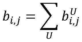
- the contribution to grid location b - j is computed according to the length of the detection line that passes that particular grid location.
- back projection of detection line is performed on two different maps comprising the grid shown in figure 6c.
- the first map is used to calculate back-projection values using the horizontal sets (Uxi, Ux2 , Ux3, ... ) and the second map is used to calculate back-projection values using the vertical sets (U y i, U y2 , U y3 , . . . ).
- step 540 the value of each grid location is compared with a threshold value to determine the presence of contamination.
- the grid coordinate (x 2 , y4) from figure 6c is determined to comprise contamination on the surface of the panel.
- step 550 shown in figure 6f the contaminated region is indicated on a display to a user with an instruction to clean the contaminated region of the panel.
- a triangulation technique is used to determine the location of contamination on the panel.
- the highest ratio from set (Rxi, Rx2, Rx3...) is determined.
- the direction of the weakest detection line corresponding to the highest ratio from set (Rxi, R x2 , R x3 ...) is determined.
- the highest ratio from set (R y i, R y2 , R y3 %) is determined.
- the direction of the weakest detection line corresponding to the highest ratio from set (R y i, R y2 , R y3 ...) is determined.
- Triangulating the direction of the weakest detection line corresponding to the highest ratio from set (Rxi, R x2 , Rx3...) with the direction of the weakest detection line corresponding to the highest ratio from set (R y i, R y2 , Ry3 ...) will provide an indication of the most contaminated region of the panel.
- FIG. 8 shows an example of a data processing device 10, which includes an input 810 for receiving the projection signals.
- the device 10 further includes a global contamination element (or means) 820 for performing steps 310-340, a regional contamination detection element (or means) 830 for performing steps 510-550, and an output element (or means) 840 for providing global and regional contamination determination values via an output 850.
- the device 10 may be implemented by special-purpose software (or firmware) run on one or more general-purpose or special-purpose computing devices.
- each "element” or “means” of such a computing device refers to a conceptual equivalent of a method step; there is not always a one-to-one correspondence between elements/means and particular pieces of hardware or software routines.
- One piece of hardware sometimes comprises different means/elements.
- a processing unit may serve as one element/means when executing one instruction, but serve as another element/means when executing another instruction.
- one element/means may be implemented by one instruction in some cases, but by a plurality of instructions in some other cases.
- the software controlled device 10 may include one or more processing units, e.g. a CPU ("Central Processing Unit"), a DSP ("Digital Signal Processor"), an ASIC ("Application-Specific Integrated Circuit”), discrete analogue and/or digital
- processing units e.g. a CPU ("Central Processing Unit"), a DSP ("Digital Signal Processor"), an ASIC ("Application-Specific Integrated Circuit"), discrete analogue and/or digital
- the device 10 may further include a system memory and a system bus that couples various system components including the system memory to the processing unit.
- the system bus may be any of several types of bus structures including a memory bus or memory controller, a peripheral bus, and a local bus using any of a variety of bus architectures.
- the system memory may include computer storage media in the form of volatile and/or non-volatile memory such as read only memory (ROM), random access memory (RAM) and flash memory.
- the special-purpose software and associated control parameter values may be stored in the system memory, or on other removable/non-removable volatile/nonvolatile computer storage media which is included in or accessible to the computing device, such as magnetic media, optical media, flash memory cards, digital tape, solid state RAM, solid state ROM, etc.
- the data processing device 10 may include one or more communication interfaces, such as a serial interface, a parallel interface, a USB interface, a wireless interface, a network adapter, etc, as well as one or more data acquisition devices, such as an AID converter.
- the special -purpose software may be provided to the device 10 on any suitable computer-readable medium, including a record medium, and a read-only memory. Touch Display
- the contamination detection function takes advantage of existing FTIR touch components such as those described in PCT publication WO2014042576 A3 "Touch force estimation in an FTIR-based projection- type touch-sensing apparatus".
- WO2014042576 is used to determine contact between an object and the panel
- an embodiment of the present invention uses the same apparatus for determination of surface contamination of the panel.
- surface 4 is also a touch sensitive surface and processing element 10 is configured to determine, based on output signals of the light detectors 3, a light energy value for each light path; to generate a transmission value for each light path based on the light energy value; and to operate an image reconstruction algorithm on at least part of the thus-generated transmission values so as to determine the position of an object on the touch surface.
- the image reconstruction algorithm may be an algorithm for transmission tomography with a fan beam geometry.
- the apparatus may be configured to be switchable between a touch detection mode and a contamination detection mode.
- the contamination detection runs in parallel to the touch detection and uses the same signals recorded for touch determination.
- the contamination detection runs in parallel to the touch detection and uses the same signals recorded for touch determination.
- contamination detection may be executed on separate processing hardware or on the same signal processing hardware provided for touch determination.
- the contamination detection process runs at a lower frame rate than a touch detection process.
- the contamination detection process may be configured to collect and process only part of the contamination data in each frame. For example, contamination detection process is operated to use only emitters 1- 5 from a first frame and collect the corresponding detector data, and then use only emitters 6-10 in the second frame etc. until all the emitters have been used. This method allows a reduction in the amount of processing used but leads to a slower update of the contamination mapping.
- detection of contamination is substantially less latency critical.
- embodiments of the invention may use the same recorded signal values to determine surface contamination as those recorded to determine touch, it is important to note that the techniques for determining touch as described by the prior art are fundamentally different to the techniques described herein for determining surface contamination.
- the contamination detection apparatus is overlaid on or integrated into a display device or monitor.
- This may be part of an FTIR type touch system (for example, a touch display) or just a contamination detection panel for a display, e.g. for applications requiring exceptional optical clarity.
- Contamination handling module 23 is configured to provide alerts to a user via an operating system call, a direct software interaction, or a hardware alert e.g. via an LED, separate display, or sound alert.
- Figures 7a - 7c show embodiment of a software interface for providing contamination information to the user.
- a determination of the global contamination is used to display a contamination value and corresponding
- the contamination value and corresponding bar are used to indicate the general level of surface contamination on the screen and provides a prompt to the user to clean the screen.
- the contamination value is updated as the user cleans the screen, providing the user with a real time update on the effectiveness of his cleaning efforts.
- a determination of the regional contamination is used to display a region of the screen that is contaminated.
- contaminated region of the screen is marked 'clean here' as an indication to the user that the screen should be cleaned.
- the size and position of a 'clean here' box corresponds to the position and size of the contaminated region.
- the size or colour of the box may correspond to the degree of
- the contamination value is updated as the user cleans the screen, providing the user with a real time update on the
- the size of the box may shrink to indicate less contamination.
- the colour of the box fades from a first colour (e.g. red) to a second colour (e.g. green) as the screen becomes cleaner.
- the 'clean here' box is repositioned from a first area to a second area of contamination once a first area of contamination has been successfully cleaned.
- a regional contamination indicator is combined with the global contamination indicator. This provides the user with an indicator of which section of the panel to focus his or her cleaning efforts, as well as an indicator of their overall progress towards a completely clean screen.
- the software interface is configured to provide the user with an indication of success once either the regional contamination or the global contamination has been successfully cleaned.
- the user interface is configured to provide an indication of the estimated loss of clarity in contaminated regions of the panel.
- the estimated loss of clarity may be calculated as a function of the determined regional or global contamination.
- the user interface is configured to provide a warning once either global or regional contamination passes a threshold.
- the warning may indicate the possibility and/or degree of degradation in touch performance of a touch sensitive panel.
- the warning may indicate to the user the risk of spread of infection from fluids deposited on the panel.
- the user interface is configured to provide an indication of the environment humidity and/or condensation affecting the panel in dependence on the global and/or regional contamination determinations.
- the contamination detection is used to determine whether contamination is present on optically critical applications, including solar panels, windows, museum displays, eye wear, and lenses of all types.
- contamination 7 maybe detected on both the top surface 4 and bottom surface 5 simultaneously.
Abstract
A device implements a method for detecting contamination of an FTIR-based panel. The apparatus generates projection signals representing detection lines that have propagated on a plurality of propagation paths by total internal reflection (TIR) inside a transmissive panel such that contamination on the panel surface causes attenuation (frustration) of at least one of the projection signals. The device generates a transmission value for each detection line in the transmissive panel, and determines the presence of contamination on the surface of the panel by comparing the transmission values ac- cording to at least one of the presented comparison techniques.
Description
DETECTION OF SURFACE CONTAMINATION
Cross-reference to Related Applications
The present application claims the benefit of Swedish patent application No. 1450796-6, filed 27-Jun-2014.
Technical Field
The present invention relates to contamination sensing systems and data processing techniques in relation to such systems.
Background
Contamination of glass surfaces by water, grease, dirt, dust, or any other substance, can be a problem in a range of circumstances. In applications such as windows or vehicle windscreens, it is important to maintain excellent optical clarity through the glass panel. In the example of the vehicle windscreen, contamination such as rain or dirt on a windscreen panel can obscure the driver's view and create a driving hazard. There is a need to detect the presence of contamination and provide a response mechanism, such as activating the use of windscreen washer fluid and windscreen wipers. US20070096015 Al describes the use of FTIR (frustrated total internal reflection) to determine the presence of rain on the surface of a vehicle windscreen by directing a beam of light into the glass windscreen. When the windscreen is clean, the beam of light is totally internally reflected and received by a sensor. When the windscreen is wet, the light is absorbed by the water and the total internal reflection is frustrated. The change in the reflective properties of the glass can be detected in order to determine the presence of rain on the glass.
Other examples of glass (or simply transparent) panels that might benefit from a means for detecting the presence of contamination may include shop windows or museum displays, where the need for optical clarity is high, while the risk of contamination from human hands is also high. Human fingers usually deposit grease on the surface of any object they touch and, over time, the build-up of grease can result in a visible dirty effect on the touched surface.
In certain applications, the presence of surface contamination on a transparent panel may have consequences that extend beyond merely degrading the optical clarity of the panel. Touch sensitive panels, such as those used on touch sensitive displays, are known to suffer from performance degradation when the touch sensitive surface is contaminated with water, finger grease, etc. This effect can be observed particularly with projected capacitive touch technology and in-glass optical touch technologies using techniques such as scatter detection or detection of light attenuation. An example of an FTIR optical touch technology which might suffer from contamination is shown in US patent 7,432,893. Further examples of touch sensitive systems operating by FTIR are disclosed in US 8,581,884, US 2013/0044073 and US 2011/0074735. Therefore, there may be a particular need for a touch sensitive surface to detect and react to surface contamination of a touch sensitive panel.
In other applications, the presence of surface contamination may represent additional problems beyond those of optical performance or touch performance. In the field of medical instruments, it may be critical that certain surfaces remain free of contamination which may host infectious agents. The use of a touch display in an operating theatre, for example, may allow surgeons to access vital information during a surgical operation. However, if the touch display becomes contaminated with fluids or dirt during the operation, it might be critical that the display is able to detect and react to the contamination.
Therefore, there is a need for an accurate and fast method of determining contamination of a transparent panel which can provide contamination information across a contamination sensitive area. Summary
A first aspect of the invention describes a surface contamination sensing apparatus, comprising: a light transmissive element that defines a surface; a set of emitters arranged to emit beams of light into the light transmissive element, wherein the beams of light propagate inside the light transmissive element while illuminating the surface such that an object or surface contamination on the surface causes an attenuation of the propagating light, a set of light detectors arranged proximal to the surface to
receive light from the set of emitters on a plurality of light paths, a processing element configured to: determine, based on output signals from the light detectors, a
transmission value for each light path; generate a transmission variance value in dependence on a comparison between transmission values of a first subset of light paths of a superset of light paths and transmission values of a second subset of light paths of the superset of light paths, determine a surface contamination on the surface in a region defined by the first and second subsets of light paths in dependence on the transmission variance value.
The transmission variance may be generated in dependence on a comparison of a lowest transmission value of the first subset of light paths and a highest transmission value of the second subset of light paths. This allows the highest ratio possible to be generated and can increase the sensitivity of the system when the quantity of contamination is low. Alternatively, the transmission variance value may be generated in dependence on a comparison of an average value of the transmission values of the first subset of light paths and an average value of the transmission values of the second subset of light paths. This variation is less susceptible to noise but provides less sensitivity to contamination.
Preferably, the first and second subsets of light paths comprise light paths with an angle within 40 degrees of any other member of their respective set. The first and second subsets of light paths may comprise light paths having a length with a maximum variance of 10% from the length of any other member of their respective set. The first subset of light paths may comprise light paths originating from the same emitter. Also, the second subset of light paths may comprise light paths originating from the same emitter. This ensures that the light paths of a set which are compared are all of a similar length and should have a similar transmission value when the panel is clean. This increases sensitivity to contamination of the panel. Preferably, the average length of light paths of first subset is longer than average length of light paths of second subset. This increases the difference between the highest and lowest transmission value.
Preferably, the surface contamination is determined in dependence on a comparison of the transmission variance value with a predetermined threshold. This
allows a threshold to be selected such that if the transmission variance value exceeds the value, an action may be taken by the system (e.g. notify the user of the contamination).
In one embodiment, each of the first and second subset of light paths each comprise a single light path and wherein the transmission variance value is a ratio between the transmission value of the light path of the first subset and a transmission value of the light path of the second subset. This arrangement allows the comparison of individual light paths within the superset, leading to a potentially more regionally focused contamination detection. The light path of the first subset may be the light path of the superset of light paths with the lowest transmission value and light path of the second subset may be the light path of the superset of light paths with the highest transmission value. This allows the highest ratio possible to be generated and can increase the sensitivity of the system when the quantity of contamination is low. In this embodiment, the superset of light paths may be configured to comprise light paths with an angle within 40 degrees of any other member of the superset and may be configured to have a length with a maximum variance of 10% from the length of any other member of the superset. Preferably, the superset of light paths comprises light paths originating from the same emitter.
The processing element may be further configured to: generate a plurality of transmission variance values for a plurality of supersets of light paths, and determine a surface contamination on the surface (1) in a region defined by the plurality of supersets of light paths in dependence on the average of the plurality of transmission variance values. This can provide a determination of a global contamination of the panel.
Alternatively, the processing element may be further configured to: generate a plurality of transmission variance values for a plurality of supersets of light paths, and determine, from the plurality of transmission variance values, a map of a surface contamination on at least a portion of the surface. The map of the surface contamination on at least a portion of the surface may be generated by means of a back-projection of the plurality of transmission variance values onto the map. This can provide a regional determination of the panel.
A second aspect describes a method in a contamination detecting apparatus, said contamination detecting apparatus comprising: a light transmissive element that defines
a surface; a set of emitters arranged to emit beams of light into the light transmissive element, wherein the beams of light propagate inside the light transmissive element while illuminating the surface such that an object or surface contamination on the surface causes an attenuation of the propagating light, and a set of light detectors arranged proximal to the surface to receive light from the set of emitters on a plurality of light paths: said method comprising the steps of: determining, based on output signals of the light detectors, a transmission value for each light path; generating a transmission variance value in dependence on a comparison between transmission values of a first subset of light paths of a superset of light paths and transmission values of a second subset of light paths of the superset of light paths, determining a surface contamination on the surface in a region defined by the first and second subsets of light paths in dependence on the transmission variance value.
A third aspect describes a computer-readable medium storing processing instructions that, when executed by a processor, performs the method of the second aspect.
Brief Description of Drawings
Embodiments of the invention will now be described in more detail with reference to the accompanying schematic drawings.
Figs la- lb are section and top plan views of an FTIR-based system of projection- type.
Fig. 2 is a flowchart of a data extraction process in the system of Fig. 1.
Fig. 3 is a flowchart of a global contamination detection process.
Fig. 4a-4b illustrate a globally contaminated panel and the detection lines used to detect the global contamination.
Fig. 5 is a flowchart of a regional contamination detection process.
Figs 6a-6f a regionally contaminated panel and the detection lines used to detect the regional contamination.
Figs 7a-7c show user interface configurations to alert the user to the presence, type, and location of the contamination.
Fig. 8 shows an example of a data processing device.
Detailed Description of Example Embodiments
Throughout the following description, the same reference numerals are used to identify corresponding elements.
Panel
Figs 1A-1B illustrate an example embodiment of a surface contamination detection apparatus 100 that is based on the concept of FTIR (Frustrated Total Internal Reflection), also denoted "FTIR system". The apparatus operates by transmitting light inside a panel 1, from light emitters 2 to light sensors or detectors 3, so as to illuminate a surface 4 from within the panel 1. The panel 1 is made of solid material in one or more layers and may have any shape. The panel 1 defines an internal radiation propagation channel, in which light propagates by internal reflections. In the example of Fig. 1, the propagation channel is defined between the boundary surfaces 4, 5 of the panel 1, where the top surface 4 allows the propagating light to interact with contamination 7. This is achieved by injecting the light into the panel 1 such that the light is reflected by total internal reflection (TIR) in the surface 4 as it propagates through the panel 1. The light may be reflected by TIR in the bottom surface 5 or against a reflective coating thereon. It is also conceivable that the propagation channel is spaced from the bottom surface 5, e.g. if the panel comprises multiple layers of different materials.
Attenuation
The apparatus 100 allows surface contamination 7 that is in contact with the surface 4 to interact with the propagating light. In this interaction, part of the light may be scattered by the surface contamination 7, part of the light may be absorbed by the surface contamination 7, and part of the light may continue to propagate in its original direction across the panel 1. Thus, the surface contamination 7 causes a local frustration of the total internal reflection, which leads to a decrease in the energy (power/intensity) of the transmitted light, as indicated by the thinned lines downstream of the surface contamination 7 in Fig. 1 A.
Emitters
The emitters 2 are distributed along the perimeter of the surface 4 to generate a corresponding number of light sheets inside the panel 1. In the example of Fig. IB, each emitter 2 generates a beam of light that expands in the plane of the panel 1 while propagating in the panel 1. Each beam propagates from one or more entry or incoupling points on the panel 1.
Detectors
The sensors 3 are distributed along the perimeter of the surface 4 to receive the light from the emitters 2 at a number of spaced-apart outcoupling points on the panel 1. It should be understood that the incoupling and outcoupling points merely refer to the position where the beam enters and leaves, respectively, the panel 1. Thus, one emitter/sensor may be optically coupled to a number of incoupling/outcoupling points. As used herein, a "detection line" is defined as the line extending from one incoupling point to one outcoupling point. In the example of Fig. IB, however, the detection lines D are defined by individual emitter-sensor pairs.
Signal Processor
The sensors 3 collectively provide an output signal, which is received and samp- led by a signal processor 10. The output signal contains a number of sub-signals, also denoted "projection signals", each representing the energy of light emitted by a certain light emitter 2 and received by a certain light sensor 3. The signal processor 10 may need to process the output signal for separation of the individual projection signals. Conceptually, the apparatus 100 is considered to define a grid of detection lines D on the surface 4, where each detection line D corresponds to a light propagation path from an emitter 2 to a sensor 3, as projected onto the surface 4. Thus, the projection signals represent the received energy or power of light on the individual detection lines D. It is realized that the surface contamination 7 results in a decrease (attenuation) of the received energy on one or more detection lines D.
As will be explained below, the signal processor 10 may be configured to process the projection signals to provide transmission values which may then be used to
determine one or more variances in the attenuation of the individual signals. The variances can then be processed according to the algorithms of the present invention to determine a surface contamination of the panel surface 4. Controller
In the illustrated example, the apparatus 100 also includes a controller 12 which is connected to selectively control the activation of the emitters 2 and, possibly, the readout of data from the sensors 3. The signal processor 10 and the controller 12 may be configured as separate units, or they may be incorporated in a single unit. One or both of the signal processor 10 and the controller 12 may be at least partially implemented by software executed by a processing unit 14.
Similar sequence methods
It is to be understood that Figs, la and lb merely illustrates one example of an FTIR system. For example, the detection lines may instead be generated by sweeping or scanning one or more beams of light inside the panel 1, and the light may instead be coupled into and out of the panel 1 via the top and bottom surfaces 4, 5, e.g. by the use of dedicated coupling elements attached to the panel 1. Prior art documents disclosing alternative FTIR systems are listed in the Background section, all of which are incorporated herein by this reference. The inventive concept may be applied to such alternative FTIR systems as well.
Data Extraction Process
Fig. 2 is a flow chart of a contamination detection process in an FTIR system. The process involves a sequence of steps 20-23 that are repeatedly executed, e.g. by the signal processor 10 (Fig. 1). In the context of this description, each sequence of steps 20-23 is denoted a frame or an iteration.
Each frame starts by a data collection step 20, in which measurement values are obtained from the light sensors 3 in the FTIR system, typically by sampling a value from each of the aforesaid projection signals. The data collection step 20 results in one transmission value for each detection line. It may be noted that the data may, but need
not, be collected for all available detection lines in the FTIR system. The data collection step 20 may also include pre-processing of the measurement values, e.g. filtering for noise reduction, normalisation with a respective reference value, applying a logarithm on each measurement value.
In step 21, a determination of a global contamination on the surface of panel 1 of the FTIR system is performed according to the methods described below. In step 22, a determination of the regional contamination of the surface of panel 1 of the FTIR system is performed according to the methods described below. In step 23, the contamination handling module receives the measured global and regional
contamination values and operates to perform a response e.g. notify the user of a detected contamination.
In other embodiments, global contamination detection or regional contamination detection may be performed on its own, i.e. either step 21 or step 22 would be omitted. In another embodiment, step 21 and step 22 are reversed.
Surface Contamination Detection Algorithm
Below are described two methods of determining contamination on the surface of the panel. Global contamination determination
Fig. 3 is a flow chart of a global contamination detection process in an FTIR system. The process involves a sequence of steps 310-350 that are executed each time a determination of global contamination on the panel is required. In this case, a measure of the global contamination is defined as a single measure indicating the amount of contamination covering the surface. This can therefore be used to indicate total contamination regardless of whether the contamination is localized or is spread across the entire surface of the panel. An example of contamination covering the entire surface may be dust and grime collected over a long period of time, fine water droplets dispersed across the panel from rain or other sources, etc.
To determine a value of the total contamination level on the panel, two techniques are presented. These two techniques may be used individually or independently to
determine a global contamination level or may be combined to produce a more accurate value of the global contamination level.
The first technique makes use of the fact that, on average, long detection lines will pass through more contamination than short ones. Consequently, longer detection lines are likely to be more attenuated than short ones. All detection lines suffer from a degree of attenuation due to 'bulk absorption' i.e. absorption of the light by the glass itself. However, for a clean panel, the transmission value for a long detection line will be only slightly less than the corresponding transmission value for a short detection line.
However, for a contaminated panel, the difference between the transmission value for the long detection line and the transmission value for the short detection line will increase. For a heavily contaminated panel, the difference between the transmission values is significant. Consequently, a measure of the differences in transmission values between long and short detection lines can provide a determination of the contamination in the areas crossed by the detection lines. This technique gives particularly good estimation of attenuation of the panel when the panel is uniformly contaminated.
The second technique makes use of the fact that contamination is rarely completely uniform. The transmission values are compared for a set of detection lines that have approximately the same transmission value when the panel is clean. By determining a ratio between strongest and weakest transmission values of the compared detection lines, a determination of contamination of the panel can be made. i.e. The variation between the strongest and weakest detection lines (i.e. the detection lines with the strongest and weakest transmission values) increases as the contamination has a random effect on the attenuation of the detection lines. The strongest line from this subset will be the detection line that goes through the least amount of contamination and the weakest line will go through the most amount of contamination. As the ratio between the strongest and weakest transmission value rises, the probability of the presence of contamination in the region which the lines pass through is increased
In a preferred embodiment, a combination of the two techniques is employed. In the preferred embodiment, the maximum transmission values for a set of short detection lines is compared to the minimum transmission values for a set of long detection lines. This combination of the presented techniques becomes even more suitable for
determining the global contamination level. The maximum transmission value of a relatively large set of short detection lines is the detection line that has been attenuated by the least amount of contamination. The minimum transmission value of a relatively large set of long detection lines is the detection line that has gone through the most amount of contamination. The ratio between these two transmission values is a good indicator of the global level of contamination on the panel
Implementation
Figure 4a shows a surface 4 with global contamination 17.
In step 310 of figure 3, a set of detection lines are selected for use in the contamination determination. In a preferred embodiment shown in figure 4b, detection lines from each emitter are used. For each of the emitters (xi, x2, x3...) along the short edge, a set (Uxi, Ux2 , Ux3 ...) of detection lines within ±20 degrees of the horizontal axis of the panel is selected for use with the process, i.e. Uxi is a set of detection lines from emitter xi. For each of the emitters (yi, y2, y3...) along the long edge, a set (Uyi, Uy2 , Uy3 ... ) of detection lines within ±20 degrees of the vertical axis of the panel is selected for use with the process, i.e. Uyi is a set of detection lines from emitter yi.
In step 320, the detection line with the lowest transmission values (i.e. weakest projection signal) from each of set (Uxi, Ux2 , Ux3 ...) is selected. The transmission values of the selected detection lines are summed.
In step 330, the detection line with the highest transmission values (i.e. strongest projection signals) from each of set (Uyi, Uy2 , Uy3 ...) is selected. The transmission values of the selected detection lines are summed.
In step 340, a ratio of the sum of the highest transmission values and the sum of the lowest transmission values is output as a global contamination value by the system. n m
Global Contamination =

As can be seen, both the first and second techniques described above are employed in this embodiment. However, each of these techniques may be employed
alone or independently to determine the global contamination of the panel. In one embodiment using only the first technique, the average of set (Uyi, Uy2 , Uy3 ...) is calculated and compared to the average of set (Uxi, Ux2 , Ux3 ...). The result is a ratio that increases with increasing contamination level of the panel.
In an embodiment using only the second technique, either the average or maximum ratio within the subsets is used. This means that for each subset, the ratio between the strongest and weakest detection lines is calculated. All these ratios are averaged and used as a measure of the global contamination level. Alternatively, the highest ratio is determined and used as a measure of the global contamination level.
In optional step 350, the global contamination is indicated on a display to a user with an instruction to clean the contaminated panel.
Regional contamination determination
Fig. 5 is a flow chart of a regional contamination detection process in an FTIR system. The process involves a sequence of steps 510-550 that are executed each time a determination of contamination on the panel is required which provides regional specific information about the location of the contamination.
A measure of the regional contamination is most useful when the contamination is concentrated in a small area. An example of regional contamination may be a finger smudge, a water droplet, an object resting on the surface etc.
The technique presented for regional contamination is similar to the second technique presented for global contamination determination. For a set of detection lines that have approximately the same transmission value when the panel is clean, the detection lines with the strongest and weakest transmission values respectively are determined. The ratio between the detection lines with the strongest and weakest transmission values increases as the contamination level on the panel increases. The line with the strongest transmission value from this subset will be the detection line that passes through the least amount of contamination and the detection line with the weakest transmission value will pass through the most amount of contamination.
In the technique presented for regional contamination, the ratios for a plurality of subsets of the set of detection lines are determined. Preferably, subsets each comprise
detection lines from a respective emitter, i.e. each subset has detection lines from one emitter.
For each subset, the detection line most affected by contamination (i.e. the detection line with the minimum transmission value) is determined and used to determine a direction from the single emitter of the contamination affecting the detection line. This direction is determined from the known angle of the detection line from the single emitter. If the ratio determined from the subset is small, it is determined that no real indication of a regionalized contaminated area is made by the single emitter. If the ratio determined from the subset is high, probability is high of contamination in the direction indicated by the detection line with the weakest transmission value. By combining the contamination probability with the directional information from several different subsets, it becomes possible to determine a localized region on the panel that is contaminated, using techniques such as Filtered Back Projection, FFT-based algorithms, ART (Algebraic Reconstruction Technique), SART (Simultaneous Algebraic
Reconstruction Technique), etc.
Implementation
Figure 6a shows a surface 4 with regional or local contamination 27.
In step 510 of figure 5, a set of detection lines are selected for use in the contamination determination. In a preferred embodiment shown in figure 6b, detection lines from each emitter are used. For each of the emitters (xi, x2, x3...) along the short edge, a set (Uxi, Ux2 , Ux3 ...) of detection lines within ±20 degrees of the horizontal axis is selected for use with the process. For each of the emitters (yi, y2, y3...) along the long edge, a set (Uyi, Uy2 , Uy3 ...) of detection lines within ±20 degrees of the vertical axis is selected for use with the process. It is envisaged that different angular ranges are used to determine which detection lines are included in each set. A range of between 5 degrees and 45 degrees may provide useful results.
In step 520, the detection lines with the highest and lowest transmission values from each of set Uxi, Ux2 , Ux3 are compared and a ratio (Rxi, Rx2, Rx3...) between the highest and lowest transmission values is calculated for each set. Contaminated regions of the panel are likely to produce a greater variation in the transmission values of the set
of detection lines traversing the contaminated region. This results in sets of detection lines with a higher ratio R value.
Figure 6c shows the surface 4 divided up into a grid in dependence on the horizontally and vertically facing emitters and corresponding detection line positions. In step 530, the ratio value R for each horizontal set (Uxi, Ux2 , Ux3, ... ) and vertical set (Uyi, Uy2 , Uy3, ... ) of detection lines are back projected (described below) to the grid locations covered by at least one detection line from the set. In a preferred embodiment, the weakest detection line from each set (i.e. the detection line from the set used to calculate R with the weakest transmission value) is used to determine how each grid location is affected by the ratio value R for each set.
Figure 6d shows the a map of surface 4 divided up into a grid comprising rectangular grid locations 30, each having centre point p; j.
Define py = (x, y) to be the centre points of grid locations 30 of the map. Define i = (x > y) to be the positions of the emitters, dk = (x, y) to be the positions of the detectors. The normal to the detection line given by emitter I and detector k is defined
_ _ normal(¾-e() _ (-Ay,Ax)
aS Uk'1 ~ Wdk-et - jAxZ +Ayf
In a preferred embodiment shown in figure 6e, the contribution to all centre points of grid locations in the map is computed for the weakest line 35 in each set, U. For each set, U, the minimum distance between the detection line, from emitter ex to detector dk, and all grid points (by projection onto the normal vector nk i) is computed:

For each set, U, the contribution to all grid points is computed according to
¾ = Ru■ w(Slj)
Where Rv is the ratio value calculated for the respective horizontal or vertical set and where the weight function, w, describes how much contribution a point gets depending on the distance from the detection line to the grid point. Some examples are
(s) = e~s2l <y2
if \s\ < sthreshold
if |s | > sthreshold
 if \s\≥ sthreshold
The contributions from all sets, U, are aggregated into a single map using contributions from all sets
In another embodiment, the contribution to grid location b -j is computed according to the length of the detection line that passes that particular grid location.
In a preferred embodiment, back projection of detection line is performed on two different maps comprising the grid shown in figure 6c. The first map is used to calculate back-projection values using the horizontal sets (Uxi, Ux2 , Ux3, ... ) and the second map is used to calculate back-projection values using the vertical sets (Uyi, Uy2 , Uy3, . . . ). This results in two maps, bh (accumulated using horizontal sets) and bv (accumulated using rtical sets).

such as a summing of the maps.
In step 540, the value of each grid location is compared with a threshold value to determine the presence of contamination. The grid coordinate (x2, y4) from figure 6c is determined to comprise contamination on the surface of the panel.
In optional step 550 shown in figure 6f, the contaminated region is indicated on a display to a user with an instruction to clean the contaminated region of the panel.
In an alternative embodiment of the invention, a triangulation technique is used to determine the location of contamination on the panel. First, the highest ratio from set (Rxi, Rx2, Rx3...) is determined. Then, the direction of the weakest detection line corresponding to the highest ratio from set (Rxi, Rx2, Rx3...) is determined. Similarly, the highest ratio from set (Ryi, Ry2, Ry3 ...) is determined. Then, the direction of the weakest detection line corresponding to the highest ratio from set (Ryi, Ry2, Ry3 ...) is determined. Triangulating the direction of the weakest detection line corresponding to
the highest ratio from set (Rxi, Rx2, Rx3...) with the direction of the weakest detection line corresponding to the highest ratio from set (Ryi, Ry2, Ry3 ...) will provide an indication of the most contaminated region of the panel.
Process Execution
The contamination determination in Figures 3 and 5 may be executed separately from the data collection process in Fig. 2, e.g. on separate devices or on a single device (e.g. the signal processor 10 in Fig. 1). Alternatively, the processes in Fig. 2, 3 and 5 may be integrated into one process for execution on a single device. Fig. 8 shows an example of a data processing device 10, which includes an input 810 for receiving the projection signals. The device 10 further includes a global contamination element (or means) 820 for performing steps 310-340, a regional contamination detection element (or means) 830 for performing steps 510-550, and an output element (or means) 840 for providing global and regional contamination determination values via an output 850.
Hardware Device
The device 10 may be implemented by special-purpose software (or firmware) run on one or more general-purpose or special-purpose computing devices. In this context, it is to be understood that each "element" or "means" of such a computing device refers to a conceptual equivalent of a method step; there is not always a one-to-one correspondence between elements/means and particular pieces of hardware or software routines. One piece of hardware sometimes comprises different means/elements. For example, a processing unit may serve as one element/means when executing one instruction, but serve as another element/means when executing another instruction. In addition, one element/means may be implemented by one instruction in some cases, but by a plurality of instructions in some other cases. Naturally, it is conceivable that one or more elements (means) are implemented entirely by analogue hardware components. The software controlled device 10 may include one or more processing units, e.g. a CPU ("Central Processing Unit"), a DSP ("Digital Signal Processor"), an ASIC
("Application-Specific Integrated Circuit"), discrete analogue and/or digital
components, or some other programmable logical device, such as an FPGA ("Field Programmable Gate Array"). The device 10 may further include a system memory and a system bus that couples various system components including the system memory to the processing unit. The system bus may be any of several types of bus structures including a memory bus or memory controller, a peripheral bus, and a local bus using any of a variety of bus architectures. The system memory may include computer storage media in the form of volatile and/or non-volatile memory such as read only memory (ROM), random access memory (RAM) and flash memory. The special-purpose software and associated control parameter values may be stored in the system memory, or on other removable/non-removable volatile/nonvolatile computer storage media which is included in or accessible to the computing device, such as magnetic media, optical media, flash memory cards, digital tape, solid state RAM, solid state ROM, etc. The data processing device 10 may include one or more communication interfaces, such as a serial interface, a parallel interface, a USB interface, a wireless interface, a network adapter, etc, as well as one or more data acquisition devices, such as an AID converter. The special -purpose software may be provided to the device 10 on any suitable computer-readable medium, including a record medium, and a read-only memory. Touch Display
In one embodiment of the invention, the contamination detection function takes advantage of existing FTIR touch components such as those described in PCT publication WO2014042576 A3 "Touch force estimation in an FTIR-based projection- type touch-sensing apparatus". Where the apparatus described in WO2014042576 is used to determine contact between an object and the panel, an embodiment of the present invention uses the same apparatus for determination of surface contamination of the panel.
In a preferred embodiment, surface 4 is also a touch sensitive surface and processing element 10 is configured to determine, based on output signals of the light detectors 3, a light energy value for each light path; to generate a transmission value for each light path based on the light energy value; and to operate an image reconstruction
algorithm on at least part of the thus-generated transmission values so as to determine the position of an object on the touch surface. The image reconstruction algorithm may be an algorithm for transmission tomography with a fan beam geometry.
In one embodiment, the apparatus may be configured to be switchable between a touch detection mode and a contamination detection mode. In an alternative
embodiment, the contamination detection runs in parallel to the touch detection and uses the same signals recorded for touch determination. In this embodiment, the
contamination detection may be executed on separate processing hardware or on the same signal processing hardware provided for touch determination.
In one embodiment, the contamination detection process runs at a lower frame rate than a touch detection process. Alternatively, the contamination detection process may be configured to collect and process only part of the contamination data in each frame. For example, contamination detection process is operated to use only emitters 1- 5 from a first frame and collect the corresponding detector data, and then use only emitters 6-10 in the second frame etc. until all the emitters have been used. This method allows a reduction in the amount of processing used but leads to a slower update of the contamination mapping. However, compared with touch detection, detection of contamination is substantially less latency critical. Furthermore, there should be no changes in contamination during the time when the contamination detection process is used as it is preferably employed when there are no fingers present on the touch panel.
Although embodiments of the invention may use the same recorded signal values to determine surface contamination as those recorded to determine touch, it is important to note that the techniques for determining touch as described by the prior art are fundamentally different to the techniques described herein for determining surface contamination.
User Alerts
In one embodiment of the invention, the contamination detection apparatus is overlaid on or integrated into a display device or monitor. This may be part of an FTIR type touch system (for example, a touch display) or just a contamination detection panel for a display, e.g. for applications requiring exceptional optical clarity. Contamination
handling module 23 is configured to provide alerts to a user via an operating system call, a direct software interaction, or a hardware alert e.g. via an LED, separate display, or sound alert.
Figures 7a - 7c show embodiment of a software interface for providing contamination information to the user. In figure 7a, a determination of the global contamination is used to display a contamination value and corresponding
'contamination bar' to a user. The contamination value and corresponding bar are used to indicate the general level of surface contamination on the screen and provides a prompt to the user to clean the screen. In one embodiment, the contamination value is updated as the user cleans the screen, providing the user with a real time update on the effectiveness of his cleaning efforts.
In figure 7b, a determination of the regional contamination is used to display a region of the screen that is contaminated. In the embodiment shown, contaminated region of the screen is marked 'clean here' as an indication to the user that the screen should be cleaned. In one embodiment, the size and position of a 'clean here' box corresponds to the position and size of the contaminated region. In an alternative embodiment, the size or colour of the box may correspond to the degree of
contamination in that region. In one embodiment, the contamination value is updated as the user cleans the screen, providing the user with a real time update on the
effectiveness of his or her cleaning efforts, e.g. as the indicated portion of the screen is cleaned, the size of the box may shrink to indicate less contamination. Alternatively, the colour of the box fades from a first colour (e.g. red) to a second colour (e.g. green) as the screen becomes cleaner.
In one embodiment, the 'clean here' box is repositioned from a first area to a second area of contamination once a first area of contamination has been successfully cleaned.
In an embodiment shown in figure 7c, a regional contamination indicator is combined with the global contamination indicator. This provides the user with an indicator of which section of the panel to focus his or her cleaning efforts, as well as an indicator of their overall progress towards a completely clean screen.
In other embodiments of the invention, the software interface is configured to provide the user with an indication of success once either the regional contamination or the global contamination has been successfully cleaned.
In another embodiment of the invention, the user interface is configured to provide an indication of the estimated loss of clarity in contaminated regions of the panel. The estimated loss of clarity may be calculated as a function of the determined regional or global contamination.
In another embodiment of the invention, the user interface is configured to provide a warning once either global or regional contamination passes a threshold. The warning may indicate the possibility and/or degree of degradation in touch performance of a touch sensitive panel. In an alternative embodiment, the warning may indicate to the user the risk of spread of infection from fluids deposited on the panel.
In another embodiment of the invention, the user interface is configured to provide an indication of the environment humidity and/or condensation affecting the panel in dependence on the global and/or regional contamination determinations.
Non- Touch Panel
In other embodiment, the contamination detection is used to determine whether contamination is present on optically critical applications, including solar panels, windows, museum displays, eye wear, and lenses of all types.
In one embodiment, contamination 7 maybe detected on both the top surface 4 and bottom surface 5 simultaneously.
While the invention has been described in connection with what is presently considered to be the most practical and preferred embodiments, it is to be understood that the invention is not to be limited to the disclosed embodiments, but on the contrary, is intended to cover various modifications and equivalent arrangements included within the spirit and the scope of the appended claims.
Claims
1. A surface contamination sensing apparatus, comprising:
a light transmissive element (1) that defines a surface (4);
a set of emitters (2) arranged to emit beams of light into the light transmissive element (1),
wherein the beams of light propagate inside the light transmissive element (1) while illuminating the surface (4) such that surface contamination on the surface (4) causes an attenuation of the propagating light,
a set of light detectors (3) arranged proximal to the surface (4) to receive light from the set of emitters (2) on a plurality of light paths,
a processing element (10) configured to:
determine, based on output signals from the light detectors (3), a transmission value for each light path;
generate a transmission variance value in dependence on a comparison between transmission values of a first subset of light paths of a superset of light paths and transmission values of a second subset of light paths of the superset of light paths, determine a surface contamination on the surface (4) in a region defined by the first and second subsets of light paths in dependence on the transmission variance value.
2. The apparatus of claim 1, wherein the transmission variance is generated in dependence on a comparison of a lowest transmission value of the first subset of light paths and a highest transmission value of the second subset of light paths.
3. The apparatus of claim 1, wherein the transmission variance value is generated in dependence on a comparison of an average value of the transmission values of the first subset of light paths and an average value of the transmission values of the second subset of light paths.
4. The apparatus of any preceding claim, wherein the first and second subsets of light paths comprise light paths with an angle within 40 degrees of any other member of their respective set.
5. The apparatus of any preceding claim, wherein the first and second subsets of light paths comprise light paths having a length with a maximum variance of 10% from the length of any other member of their respective set.
6. The apparatus of any preceding claim, wherein the average length of light paths of the first subset is longer than average length of light paths of the second subset
7. The apparatus of any preceding claim, wherein the first subset of light paths comprises light paths originating from the same emitter.
8. The apparatus of any preceding claim, wherein the second subset of light paths comprises light paths originating from the same emitter.
9. The apparatus of any preceding claim, wherein surface contamination is determined in dependence on a comparison of the transmission variance value with a predetermined threshold.
10. The apparatus of any preceding claim, wherein the first subset of light paths are substantially perpendicular to the second subset of light paths.
11. The apparatus of claim 1, wherein each of the first and second subset of light paths each comprise a single light path and wherein the transmission variance value is a ratio between the transmission value of the light path of the first subset and a transmission value of the light path of the second subset.
12. The apparatus of claim 11, wherein the light path of the first subset is the light path of the superset of light paths with the lowest transmission value and light path of
the second subset is the light path of the superset of light paths with the highest transmission value.
13. The apparatus of any of claims 11 to 12, wherein the superset of light paths comprises light paths with an angle within 40 degrees of any other member of the superset.
14. The apparatus of any of claims 11 to 13, wherein the superset of light paths comprises light paths having a length with a maximum variance of 10% from the length of any other member of the superset.
15. The apparatus of any of claims 11 to 14, wherein the superset of light paths comprises light paths originating from the same emitter.
16. The apparatus of any of claims 11 to 15, the processing element further configured to:
generate a plurality of transmission variance values for a plurality of supersets of light paths, and
determine a surface contamination on the surface (4) in a region defined by the plurality of supersets of light paths in dependence on the average of the plurality of transmission variance values.
17. The apparatus of any of claims 11 to 15, the processing element further configured to:
generate a plurality of transmission variance values for a plurality of supersets of light paths, and
determine, from the plurality of transmission variance values, a map of a surface contamination on at least a portion of the surface (4).
18. The apparatus of claim 17, wherein the map of the surface contamination on at least a portion of the surface (4) is generated by means of a back-projection of the plurality of transmission variance values onto the map.
19. A method in a contamination detecting apparatus, said contamination detecting apparatus comprising:
a light transmissive element (1) that defines a surface (4);
a set of emitters (2) arranged to emit beams of light into the light transmissive element (1),
wherein the beams of light propagate inside the light transmissive element (1) while illuminating the surface (4) such that surface contamination on the surface (4) causes an attenuation of the propagating light, and
a set of light detectors (3) arranged proximal to the surface (4) to receive light from the set of emitters (2) on a plurality of light paths:
said method comprising the steps of:
determining, based on output signals from the light detectors (3), a transmission value for each light path;
generating a transmission variance value in dependence on a comparison between transmission values of a first subset of light paths of a superset of light paths and transmission values of a second subset of light paths of the superset of light paths, determining a surface contamination on the surface (4) in a region defined by the first and second subsets of light paths in dependence on the transmission variance value.
20. A computer-readable medium storing processing instructions that, when executed by a processor, performs the method according to claim 19.
Priority Applications (2)
| Application Number | Priority Date | Filing Date | Title |
|---|---|---|---|
| US15/317,360 US10161886B2 (en) | 2014-06-27 | 2015-06-22 | Detection of surface contamination |
| EP15812234.1A EP3161594A4 (en) | 2014-06-27 | 2015-06-22 | Detection of surface contamination |
Applications Claiming Priority (2)
| Application Number | Priority Date | Filing Date | Title |
|---|---|---|---|
| SE1450796 | 2014-06-27 | ||
| SE1450796-6 | 2014-06-27 |
Publications (1)
| Publication Number | Publication Date |
|---|---|
| WO2015199602A1 true WO2015199602A1 (en) | 2015-12-30 |
Family
ID=54938539
Family Applications (1)
| Application Number | Title | Priority Date | Filing Date |
|---|---|---|---|
| PCT/SE2015/050724 WO2015199602A1 (en) | 2014-06-27 | 2015-06-22 | Detection of surface contamination |
Country Status (3)
| Country | Link |
|---|---|
| US (1) | US10161886B2 (en) |
| EP (1) | EP3161594A4 (en) |
| WO (1) | WO2015199602A1 (en) |
Cited By (5)
| Publication number | Priority date | Publication date | Assignee | Title |
|---|---|---|---|---|
| EP3333685A4 (en) * | 2016-10-31 | 2018-08-08 | Shenzhen Goodix Technology Co., Ltd. | Touchscreen wet state detection method and capacitive touch device |
| EP3406269A1 (en) * | 2017-05-23 | 2018-11-28 | Koninklijke Philips N.V. | Safety improvement for uv applications by monitoring changes in uv outcoupling |
| US20210173514A1 (en) * | 2016-12-07 | 2021-06-10 | Flatfrog Laboratories Ab | Touch device |
| US20210247327A1 (en) * | 2019-05-28 | 2021-08-12 | Pixart Imaging Inc. | Electronic device which can determine a dirtiness level |
| US11893189B2 (en) | 2020-02-10 | 2024-02-06 | Flatfrog Laboratories Ab | Touch-sensing apparatus |
Families Citing this family (43)
| Publication number | Priority date | Publication date | Assignee | Title |
|---|---|---|---|---|
| US10853873B2 (en) | 2008-10-02 | 2020-12-01 | Ecoatm, Llc | Kiosks for evaluating and purchasing used electronic devices and related technology |
| SE533704C2 (en) | 2008-12-05 | 2010-12-07 | Flatfrog Lab Ab | Touch sensitive apparatus and method for operating the same |
| US10168835B2 (en) | 2012-05-23 | 2019-01-01 | Flatfrog Laboratories Ab | Spatial resolution in touch displays |
| US10019113B2 (en) | 2013-04-11 | 2018-07-10 | Flatfrog Laboratories Ab | Tomographic processing for touch detection |
| WO2015005847A1 (en) | 2013-07-12 | 2015-01-15 | Flatfrog Laboratories Ab | Partial detect mode |
| US10126882B2 (en) | 2014-01-16 | 2018-11-13 | Flatfrog Laboratories Ab | TIR-based optical touch systems of projection-type |
| US10146376B2 (en) | 2014-01-16 | 2018-12-04 | Flatfrog Laboratories Ab | Light coupling in TIR-based optical touch systems |
| WO2015199602A1 (en) | 2014-06-27 | 2015-12-30 | Flatfrog Laboratories Ab | Detection of surface contamination |
| CA2964214C (en) | 2014-10-02 | 2020-08-04 | ecoATM, Inc. | Wireless-enabled kiosk for recycling consumer devices |
| CA2964223C (en) | 2014-10-02 | 2020-04-14 | ecoATM, Inc. | Application for device evaluation and other processes associated with device recycling |
| EP3250993B1 (en) | 2015-01-28 | 2019-09-04 | FlatFrog Laboratories AB | Dynamic touch quarantine frames |
| US10318074B2 (en) | 2015-01-30 | 2019-06-11 | Flatfrog Laboratories Ab | Touch-sensing OLED display with tilted emitters |
| EP3537269A1 (en) | 2015-02-09 | 2019-09-11 | FlatFrog Laboratories AB | Optical touch system |
| WO2016140612A1 (en) | 2015-03-02 | 2016-09-09 | Flatfrog Laboratories Ab | Optical component for light coupling |
| EP3268240B1 (en) * | 2015-03-09 | 2020-02-26 | Jaguar Land Rover Limited | Windshield monitoring system |
| EP3113477B1 (en) * | 2015-06-30 | 2017-08-02 | Axis AB | Monitoring camera |
| EP4075246A1 (en) | 2015-12-09 | 2022-10-19 | FlatFrog Laboratories AB | Stylus for optical touch system |
| US10269110B2 (en) | 2016-06-28 | 2019-04-23 | Ecoatm, Llc | Methods and systems for detecting cracks in illuminated electronic device screens |
| WO2018096430A1 (en) | 2016-11-24 | 2018-05-31 | Flatfrog Laboratories Ab | Automatic optimisation of touch signal |
| US10963104B2 (en) | 2017-02-06 | 2021-03-30 | Flatfrog Laboratories Ab | Optical coupling in touch-sensing systems |
| EP3602257A4 (en) | 2017-03-22 | 2021-01-13 | Flatfrog Laboratories | Eraser for touch displays |
| US10144356B2 (en) | 2017-03-24 | 2018-12-04 | Ford Global Technologies, Llc | Condensation detection for vehicle surfaces via light transmitters and receivers |
| CN110663015A (en) | 2017-03-28 | 2020-01-07 | 平蛙实验室股份公司 | Touch sensitive device and method for assembly |
| CN111052058B (en) | 2017-09-01 | 2023-10-20 | 平蛙实验室股份公司 | Improved optical component |
| US10053059B1 (en) | 2017-10-04 | 2018-08-21 | Ford Global Technologies, Llc | Detection and identification of opaqueness of vehicle windows |
| US10732761B2 (en) * | 2017-12-06 | 2020-08-04 | Paypal, Inc. | Arranging content based on detection of a substance on display |
| US11567610B2 (en) | 2018-03-05 | 2023-01-31 | Flatfrog Laboratories Ab | Detection line broadening |
| US10654450B2 (en) | 2018-09-11 | 2020-05-19 | Rockwell Automation Technologies, Inc. | Droplet sensor |
| US11039899B2 (en) | 2018-09-28 | 2021-06-22 | American Sterilizer Company | Surgical lighting system sterile field encroachment indicator |
| US11943563B2 (en) | 2019-01-25 | 2024-03-26 | FlatFrog Laboratories, AB | Videoconferencing terminal and method of operating the same |
| CN109829904B (en) * | 2019-01-29 | 2022-01-14 | 京东方科技集团股份有限公司 | Method and device for detecting dust on screen, electronic equipment and readable storage medium |
| WO2020167849A1 (en) | 2019-02-12 | 2020-08-20 | Ecoatm, Llc | Connector carrier for electronic device kiosk |
| KR20210126068A (en) | 2019-02-12 | 2021-10-19 | 에코에이티엠, 엘엘씨 | Kiosks for evaluating and purchasing used electronic devices |
| JP2021530793A (en) * | 2019-02-18 | 2021-11-11 | エコエーティーエム, エルエルシー | Neural networks based on physical state assessment of electronic devices, and associated systems and methods |
| US11137485B2 (en) | 2019-08-06 | 2021-10-05 | Waymo Llc | Window occlusion imager near focal plane |
| US11922467B2 (en) | 2020-08-17 | 2024-03-05 | ecoATM, Inc. | Evaluating an electronic device using optical character recognition |
| US11457204B1 (en) | 2020-11-06 | 2022-09-27 | Waymo Llc | Localized window contaminant detection |
| JP2022182376A (en) * | 2021-05-28 | 2022-12-08 | セイコーエプソン株式会社 | Display apparatus, display control method for display apparatus, and display control program |
| US11644411B2 (en) | 2021-06-17 | 2023-05-09 | Rosemount Aerospace Inc. | Window contamination sensor |
| WO2022264115A1 (en) * | 2021-06-19 | 2022-12-22 | Agp America S.A. | Automotive glazing with safety status detection |
| US20230055880A1 (en) * | 2021-08-18 | 2023-02-23 | Robert Bosch Gmbh | Systems and methods for detecting windshield cracks |
| CN113866135A (en) * | 2021-09-24 | 2021-12-31 | 深圳市华腾半导体设备有限公司 | Pollution detection method, light splitting management method and system |
| US20230152429A1 (en) * | 2021-11-15 | 2023-05-18 | Waymo Llc | Auto-Exposure Occlusion Camera |
Citations (5)
| Publication number | Priority date | Publication date | Assignee | Title |
|---|---|---|---|---|
| US5526422A (en) * | 1994-06-20 | 1996-06-11 | At&T Corp. | System and method for cleaning the display screen of a touch screen device |
| WO2001027867A1 (en) * | 1999-10-13 | 2001-04-19 | Elo Touchsystems, Inc. | Contaminant processing system for an acoustic touchscreen |
| US20100033444A1 (en) * | 2008-08-06 | 2010-02-11 | Panasonic Corporation | Information terminal device |
| WO2011049512A1 (en) * | 2009-10-19 | 2011-04-28 | Flatfrog Laboratories Ab | Touch surface with two-dimensional compensation |
| US20130055080A1 (en) * | 2011-08-23 | 2013-02-28 | Garmin International, Inc. | System and methods for detecting debris on a touchscreen system display screen |
Family Cites Families (511)
| Publication number | Priority date | Publication date | Assignee | Title |
|---|---|---|---|---|
| FR1452041A (en) | 1965-04-26 | 1966-02-25 | Electronique & Automatisme Sa | Communication device with an electronic calculator |
| US3440426A (en) | 1966-01-11 | 1969-04-22 | Us Navy | Solar attitude encoder |
| US3673327A (en) | 1970-11-02 | 1972-06-27 | Atomic Energy Commission | Touch actuable data input panel assembly |
| IT961146B (en) | 1971-03-12 | 1973-12-10 | Schlumberger Compteurs | DEVICE PERMITTING ME TO DETERMINE THE DIRECTION OF A BRIGHT RADIATION |
| FR2172828B1 (en) | 1972-02-23 | 1974-12-13 | Dassault Electronique | |
| DE2654464A1 (en) | 1976-12-01 | 1978-06-08 | Sick Optik Elektronik Erwin | PHOTOELECTRIC LIGHT RECEIVING ARRANGEMENT |
| US4129384A (en) | 1977-06-08 | 1978-12-12 | Batelle Memorial Institute | Optical extensometer |
| US4254333A (en) | 1978-05-31 | 1981-03-03 | Bergstroem Arne | Optoelectronic circuit element |
| US4209255A (en) | 1979-03-30 | 1980-06-24 | United Technologies Corporation | Single source aiming point locator |
| US4213707A (en) | 1979-04-25 | 1980-07-22 | Eastman Kodak Company | Device for improving the accuracy of optical measuring apparatus and the like |
| US4254407A (en) | 1979-07-18 | 1981-03-03 | Ncr Corporation | Data processing system having optically linked subsystems, including an optical keyboard |
| US4294543A (en) | 1979-11-13 | 1981-10-13 | Command Control & Communications Corporation | Optical system for developing point coordinate information |
| US4484179A (en) | 1980-04-16 | 1984-11-20 | At&T Bell Laboratories | Touch position sensitive surface |
| US4346376A (en) | 1980-04-16 | 1982-08-24 | Bell Telephone Laboratories, Incorporated | Touch position sensitive surface |
| US4420261A (en) | 1980-09-02 | 1983-12-13 | Lowbar, Inc. | Optical position location apparatus |
| JPS58111705A (en) | 1981-12-25 | 1983-07-02 | Mitsutoyo Mfg Co Ltd | Optical measuring device |
| US4542375A (en) | 1982-02-11 | 1985-09-17 | At&T Bell Laboratories | Deformable touch sensitive surface |
| GB2131544B (en) | 1982-12-07 | 1986-03-05 | Lowbar Inc | Optical postition location apparatus |
| US4593191A (en) | 1982-12-29 | 1986-06-03 | At&T Bell Laboratories | Pressure and optical sensitive device with deformable protrusions |
| GB8302997D0 (en) | 1983-02-03 | 1983-03-09 | Bergstrom A | Electromagnetic radiation circuit element |
| US4507557A (en) | 1983-04-01 | 1985-03-26 | Siemens Corporate Research & Support, Inc. | Non-contact X,Y digitizer using two dynamic ram imagers |
| US4550250A (en) | 1983-11-14 | 1985-10-29 | Hei, Inc. | Cordless digital graphics input device |
| US4752655A (en) | 1984-11-16 | 1988-06-21 | Nippon Telegraph & Telephone Corporation | Coordinate input device |
| US4692809A (en) | 1984-11-20 | 1987-09-08 | Hughes Aircraft Company | Integrated touch paint system for displays |
| US4673918A (en) | 1984-11-29 | 1987-06-16 | Zenith Electronics Corporation | Light guide having focusing element and internal reflector on same face |
| JPH0325219Y2 (en) | 1985-02-15 | 1991-05-31 | ||
| JPH0325220Y2 (en) | 1985-02-15 | 1991-05-31 | ||
| US4710760A (en) | 1985-03-07 | 1987-12-01 | American Telephone And Telegraph Company, At&T Information Systems Inc. | Photoelastic touch-sensitive screen |
| US4688993A (en) | 1985-03-21 | 1987-08-25 | United Technologies Corporation | Tangential link swashplate centering member |
| DE3511330A1 (en) | 1985-03-28 | 1986-10-02 | Siemens Ag | Arrangement for inputting graphic patterns |
| US5159322A (en) | 1985-04-19 | 1992-10-27 | Loebner Hugh G | Apparatus to digitize graphic and scenic information and to determine the position of a stylus for input into a computer or the like |
| US4949079A (en) | 1985-04-19 | 1990-08-14 | Hugh Loebner | Brightpen/pad graphic device for computer inputs and the like |
| US5073770A (en) | 1985-04-19 | 1991-12-17 | Lowbner Hugh G | Brightpen/pad II |
| US4688933A (en) | 1985-05-10 | 1987-08-25 | The Laitram Corporation | Electro-optical position determining system |
| US4736191A (en) | 1985-08-02 | 1988-04-05 | Karl E. Matzke | Touch activated control method and apparatus |
| JPH0762821B2 (en) | 1986-05-30 | 1995-07-05 | 株式会社日立製作所 | Touch panel input device |
| US4782328A (en) | 1986-10-02 | 1988-11-01 | Product Development Services, Incorporated | Ambient-light-responsive touch screen data input method and system |
| US4891829A (en) | 1986-11-19 | 1990-01-02 | Exxon Research And Engineering Company | Method and apparatus for utilizing an electro-optic detector in a microtomography system |
| US4868912A (en) | 1986-11-26 | 1989-09-19 | Digital Electronics | Infrared touch panel |
| US4746770A (en) | 1987-02-17 | 1988-05-24 | Sensor Frame Incorporated | Method and apparatus for isolating and manipulating graphic objects on computer video monitor |
| US4820050A (en) | 1987-04-28 | 1989-04-11 | Wells-Gardner Electronics Corporation | Solid-state optical position determining apparatus |
| FR2614711B1 (en) | 1987-04-29 | 1992-03-13 | Photonetics | METHOD AND DEVICE FOR OPERATING THE SCREEN SIGNAL OF A TOUCH SCREEN |
| FR2617620B1 (en) | 1987-07-02 | 1992-09-25 | Photonetics | OPTICAL TYPE TOUCH SCREEN |
| FR2617619B1 (en) | 1987-07-02 | 1990-01-05 | Photonetics | OPTICAL TOUCH SCREEN MOUNTING DEVICE |
| US4772763A (en) | 1987-08-25 | 1988-09-20 | International Business Machines Corporation | Data processing information input using optically sensed stylus features |
| JPH01195526A (en) | 1988-01-29 | 1989-08-07 | Sony Corp | Touch panel device |
| FR2631438B1 (en) | 1988-05-11 | 1991-06-21 | Photonetics | METHOD FOR POSITIONING AN OBJECT RELATIVE TO A PLANE, METHOD FOR MEASURING LENGTH AND DEVICES FOR CARRYING OUT SAID METHODS |
| US4988983A (en) | 1988-09-02 | 1991-01-29 | Carroll Touch, Incorporated | Touch entry system with ambient compensation and programmable amplification |
| US4986662A (en) | 1988-12-19 | 1991-01-22 | Amp Incorporated | Touch entry using discrete reflectors |
| FR2645645B1 (en) | 1989-04-06 | 1991-07-12 | Photonetics | IMPROVEMENTS IN METHODS AND DEVICES FOR DETERMINING THE ANGLE OF CONTACT OF A DROP OF LIQUID PLACED ON A SUBSTRATE |
| US5065185A (en) | 1989-08-21 | 1991-11-12 | Powers Edward A | Multi-function detecting device for a document reproduction machine |
| ES2067693T3 (en) | 1989-10-16 | 1995-04-01 | Chiroscience Ltd | CHABAL AZABICICLOHEPTANONE AND A PROCEDURE FOR ITS PREPARATION. |
| US5105186A (en) | 1990-05-25 | 1992-04-14 | Hewlett-Packard Company | Lcd touch screen |
| US6390370B1 (en) | 1990-11-15 | 2002-05-21 | Symbol Technologies, Inc. | Light beam scanning pen, scan module for the device and method of utilization |
| DE4111710C2 (en) | 1991-04-10 | 1995-01-12 | Data Stream Corp | Wireless input device for computers |
| FR2676275A1 (en) | 1991-05-07 | 1992-11-13 | Photonetics | DEVICE FOR REMOTELY MEASURING THE POSITION OF AN OBJECT. |
| US5539514A (en) * | 1991-06-26 | 1996-07-23 | Hitachi, Ltd. | Foreign particle inspection apparatus and method with front and back illumination |
| US5345490A (en) | 1991-06-28 | 1994-09-06 | General Electric Company | Method and apparatus for converting computed tomography (CT) data into finite element models |
| US5335557A (en) | 1991-11-26 | 1994-08-09 | Taizo Yasutake | Touch sensitive input control device |
| CA2060564C (en) | 1992-02-06 | 1996-05-21 | Toru Suzuki | Wireless input system for computer |
| US5483261A (en) | 1992-02-14 | 1996-01-09 | Itu Research, Inc. | Graphical input controller and method with rear screen image detection |
| CH683370A5 (en) | 1992-04-10 | 1994-02-28 | Zumbach Electronic Ag | Method and apparatus for measuring the dimension of an object. |
| CA2068191C (en) | 1992-05-07 | 1994-11-22 | Fernand Sergerie | Reinforced composite backing tape |
| US7084859B1 (en) | 1992-09-18 | 2006-08-01 | Pryor Timothy R | Programmable tactile touch screen displays and man-machine interfaces for improved vehicle instrumentation and telematics |
| US5248856A (en) | 1992-10-07 | 1993-09-28 | Microfield Graphics, Inc. | Code-based, electromagnetic-field-responsive graphic data-acquisition system |
| FI935222A (en) | 1992-11-25 | 1994-05-26 | Sumitomo Electric Industries | Foerfarande Foer detektering av foeroreningar i smaelt harts |
| JP3400485B2 (en) | 1993-03-23 | 2003-04-28 | 株式会社ワコム | Optical position detecting device and optical coordinate input device |
| US5502568A (en) | 1993-03-23 | 1996-03-26 | Wacom Co., Ltd. | Optical position detecting unit, optical coordinate input unit and optical position detecting method employing a pattern having a sequence of 1's and 0's |
| DE4334937A1 (en) | 1993-10-13 | 1995-10-05 | Siemens Ag | Computer tomograph |
| JP3135183B2 (en) | 1993-10-29 | 2001-02-13 | 株式会社ワコム | Position indicator |
| WO1995014286A1 (en) | 1993-11-17 | 1995-05-26 | Microsoft Corporation | Wireless pen computer input system |
| US5484966A (en) | 1993-12-07 | 1996-01-16 | At&T Corp. | Sensing stylus position using single 1-D image sensor |
| JPH07200137A (en) | 1993-12-28 | 1995-08-04 | Wacom Co Ltd | Position detection device and its position indicator |
| JPH07261920A (en) | 1994-03-17 | 1995-10-13 | Wacom Co Ltd | Optical position detector and optical coordinate input device |
| JP3421416B2 (en) | 1994-03-18 | 2003-06-30 | 株式会社ワコム | Position detecting device and its position indicator |
| US5525764A (en) | 1994-06-09 | 1996-06-11 | Junkins; John L. | Laser scanning graphic input system |
| US5740224A (en) | 1994-09-27 | 1998-04-14 | University Of Delaware | Cone beam synthetic arrays in three-dimensional computerized tomography |
| US5686942A (en) | 1994-12-01 | 1997-11-11 | National Semiconductor Corporation | Remote computer input system which detects point source on operator |
| US5736686A (en) | 1995-03-01 | 1998-04-07 | Gtco Corporation | Illumination apparatus for a digitizer tablet with improved light panel |
| US5764223A (en) | 1995-06-07 | 1998-06-09 | International Business Machines Corporation | Touch-screen input device using the monitor as a light source operating at an intermediate frequency |
| CA2225734C (en) | 1995-06-29 | 2006-11-14 | Lynn Wiese | Localized illumination using tir technology |
| GB9516441D0 (en) | 1995-08-10 | 1995-10-11 | Philips Electronics Uk Ltd | Light pen input systems |
| WO1997041527A1 (en) | 1996-05-01 | 1997-11-06 | Xros, Inc. | Compact, simple, 2d raster, image-building fingerprint scanner |
| JP2001502078A (en) | 1996-05-29 | 2001-02-13 | ドイッチェ テレコム アーゲー | Equipment for inputting information |
| US6067079A (en) | 1996-06-13 | 2000-05-23 | International Business Machines Corporation | Virtual pointing device for touchscreens |
| DE19631414A1 (en) | 1996-08-05 | 1998-02-19 | Daimler Benz Ag | Device for recording the retinal reflex image and superimposing additional images in the eye |
| AU723301B2 (en) | 1996-08-12 | 2000-08-24 | Elo Touchsystems, Inc. | Acoustic condition sensor employing a plurality of mutually non-orthogonal waves |
| US5767517A (en) | 1996-10-21 | 1998-06-16 | Board Of Regents -Univ. Of Ne | Hybrid resampling method for fan beam spect |
| DE69739633D1 (en) | 1996-11-28 | 2009-12-10 | Casio Computer Co Ltd | display device |
| US6061177A (en) | 1996-12-19 | 2000-05-09 | Fujimoto; Kenneth Noboru | Integrated computer display and graphical input apparatus and method |
| US6380732B1 (en) | 1997-02-13 | 2002-04-30 | Super Dimension Ltd. | Six-degree of freedom tracking system having a passive transponder on the object being tracked |
| JPH113169A (en) | 1997-06-13 | 1999-01-06 | Tokai Rika Co Ltd | Touch operation information output device |
| US6229529B1 (en) | 1997-07-11 | 2001-05-08 | Ricoh Company, Ltd. | Write point detecting circuit to detect multiple write points |
| US6480187B1 (en) | 1997-08-07 | 2002-11-12 | Fujitsu Limited | Optical scanning-type touch panel |
| US6141104A (en) | 1997-09-09 | 2000-10-31 | Image Guided Technologies, Inc. | System for determination of a location in three dimensional space |
| US6909419B2 (en) | 1997-10-31 | 2005-06-21 | Kopin Corporation | Portable microdisplay system |
| US5945980A (en) | 1997-11-14 | 1999-08-31 | Logitech, Inc. | Touchpad with active plane for pen detection |
| WO1999038149A1 (en) | 1998-01-26 | 1999-07-29 | Wayne Westerman | Method and apparatus for integrating manual input |
| US9292111B2 (en) | 1998-01-26 | 2016-03-22 | Apple Inc. | Gesturing with a multipoint sensing device |
| DE19809934A1 (en) | 1998-03-07 | 1999-09-09 | Bosch Gmbh Robert | Laser display panel with contact detection |
| AU6633798A (en) | 1998-03-09 | 1999-09-27 | Gou Lite Ltd. | Optical translation measurement |
| US6172667B1 (en) | 1998-03-19 | 2001-01-09 | Michel Sayag | Optically-based touch screen input device |
| US6748098B1 (en) | 1998-04-14 | 2004-06-08 | General Electric Company | Algebraic reconstruction of images from non-equidistant data |
| US7268774B2 (en) | 1998-08-18 | 2007-09-11 | Candledragon, Inc. | Tracking motion of a writing instrument |
| JP3827450B2 (en) | 1998-08-18 | 2006-09-27 | 富士通株式会社 | Optical scanning touch panel |
| US6972753B1 (en) | 1998-10-02 | 2005-12-06 | Semiconductor Energy Laboratory Co., Ltd. | Touch panel, display device provided with touch panel and electronic equipment provided with display device |
| JP3530758B2 (en) | 1998-12-03 | 2004-05-24 | キヤノン株式会社 | Pointer for inputting coordinates |
| JP4007705B2 (en) | 1998-11-20 | 2007-11-14 | 富士通株式会社 | Optical scanning touch panel |
| JP4245721B2 (en) | 1999-03-05 | 2009-04-02 | プラスビジョン株式会社 | Coordinate input pen |
| US6333735B1 (en) | 1999-03-16 | 2001-12-25 | International Business Machines Corporation | Method and apparatus for mouse positioning device based on infrared light sources and detectors |
| JP4097353B2 (en) | 1999-04-07 | 2008-06-11 | 富士通株式会社 | Optical scanning touch panel |
| JP4939682B2 (en) | 1999-04-27 | 2012-05-30 | エーユー オプトロニクス コーポレイション | Display device |
| DE19924448A1 (en) | 1999-05-28 | 2000-12-07 | Siemens Ag | Three-dimensional data set extraction method for magnetic resonance imaging |
| FR2794246B1 (en) | 1999-05-31 | 2001-08-10 | Saint Louis Inst | DEVICE CAPABLE OF DETERMINING THE POSITION OF AN OBJECT IN AN OXZ MARK |
| EP1188069A2 (en) | 1999-06-09 | 2002-03-20 | Beamcontrol Aps | A method for determining the channel gain between emitters and receivers |
| FR2795877B1 (en) | 1999-06-30 | 2001-10-05 | Photonetics | PARTIALLY REFLECTIVE OPTICAL COMPONENT AND LASER SOURCE INCORPORATING SUCH COMPONENT |
| JP3606138B2 (en) | 1999-11-05 | 2005-01-05 | セイコーエプソン株式会社 | Driver IC, electro-optical device and electronic apparatus |
| JP2001147772A (en) | 1999-11-19 | 2001-05-29 | Fujitsu Takamisawa Component Ltd | Touch panel |
| JP3780785B2 (en) | 1999-11-30 | 2006-05-31 | 三菱電機株式会社 | Concavity and convexity pattern detector |
| MXPA02005431A (en) | 1999-12-02 | 2003-02-12 | Elo Touchsystems Inc | Apparatus and method to improve resolution of infrared touch systems. |
| JP2001183987A (en) | 1999-12-27 | 2001-07-06 | Pioneer Electronic Corp | Cooling structure and display device using the same |
| US20040252867A1 (en) | 2000-01-05 | 2004-12-16 | Je-Hsiung Lan | Biometric sensor |
| JP3881148B2 (en) | 2000-02-18 | 2007-02-14 | 株式会社リコー | Photodetection device for coordinate detection, coordinate input / detection device, electronic blackboard, mounting position detection method, and storage medium |
| US6495832B1 (en) | 2000-03-15 | 2002-12-17 | Touch Controls, Inc. | Photoelectric sensing array apparatus and method of using same |
| WO2001078052A1 (en) | 2000-04-05 | 2001-10-18 | Dimensional Media Associates, Inc. | Methods and apparatus for virtual touchscreen computer interface controller |
| US7859519B2 (en) | 2000-05-01 | 2010-12-28 | Tulbert David J | Human-machine interface |
| US6864882B2 (en) | 2000-05-24 | 2005-03-08 | Next Holdings Limited | Protected touch panel display system |
| US6690363B2 (en) | 2000-06-19 | 2004-02-10 | Next Holdings Limited | Touch panel display system |
| US6724489B2 (en) | 2000-09-22 | 2004-04-20 | Daniel Freifeld | Three dimensional scanning camera |
| US6660964B1 (en) | 2000-09-22 | 2003-12-09 | David Benderly | Optical modification of laser beam cross section in object marking systems |
| JP2004534974A (en) | 2000-10-27 | 2004-11-18 | エロ・タッチシステムズ・インコーポレイテッド | Touch confirmation type touch screen using multiple touch sensors |
| ATE463004T1 (en) | 2000-11-06 | 2010-04-15 | Koninkl Philips Electronics Nv | METHOD FOR MEASURING THE MOTION OF AN INPUT DEVICE |
| US6648485B1 (en) | 2000-11-13 | 2003-11-18 | International Business Machines Corporation | Highly collimating tapered light guide for uniform illumination of flat panel displays |
| EP1347706B1 (en) | 2000-12-30 | 2008-05-21 | The University Of Leeds | Electrical impedance tomography |
| JP4004025B2 (en) | 2001-02-13 | 2007-11-07 | 日東電工株式会社 | Transparent conductive laminate and touch panel |
| DE10110744A1 (en) | 2001-03-07 | 2002-09-26 | Franc Godler | Large, touch-sensitive area with time and location-controlled transmitter and receiver modules |
| US6452996B1 (en) | 2001-03-16 | 2002-09-17 | Ge Medical Systems Global Technology Company, Llc | Methods and apparatus utilizing generalized helical interpolation algorithm |
| JP4768143B2 (en) | 2001-03-26 | 2011-09-07 | 株式会社リコー | Information input / output device, information input / output control method, and program |
| US6738051B2 (en) | 2001-04-06 | 2004-05-18 | 3M Innovative Properties Company | Frontlit illuminated touch panel |
| JP4812181B2 (en) | 2001-04-20 | 2011-11-09 | オリンパス株式会社 | Observation optical system, imaging optical system, and apparatus using the same |
| US6992659B2 (en) | 2001-05-22 | 2006-01-31 | Palmone, Inc. | High transparency integrated enclosure touch screen assembly for a portable hand held device |
| JP3959678B2 (en) | 2001-07-13 | 2007-08-15 | ミネベア株式会社 | Touch panel for display device |
| DE10136611C1 (en) | 2001-07-23 | 2002-11-21 | Jenoptik Laserdiode Gmbh | Optical device, for laser light emitted by laser diode device, has collimation optical element and homogenizing element using multiple reflection of laser beam |
| US6985137B2 (en) | 2001-08-13 | 2006-01-10 | Nokia Mobile Phones Ltd. | Method for preventing unintended touch pad input due to accidental touching |
| US6927384B2 (en) | 2001-08-13 | 2005-08-09 | Nokia Mobile Phones Ltd. | Method and device for detecting touch pad unit |
| US6765193B2 (en) | 2001-08-21 | 2004-07-20 | National Science And Technology Development Agency | Optical touch switch structures |
| US20030048257A1 (en) | 2001-09-06 | 2003-03-13 | Nokia Mobile Phones Ltd. | Telephone set having a touch pad device |
| US7254775B2 (en) | 2001-10-03 | 2007-08-07 | 3M Innovative Properties Company | Touch panel system and method for distinguishing multiple touch inputs |
| KR20040045490A (en) | 2001-10-09 | 2004-06-01 | 코닌클리케 필립스 일렉트로닉스 엔.브이. | Device having touch sensitivity functionality |
| US20120188206A1 (en) | 2001-11-02 | 2012-07-26 | Neonode, Inc. | Optical touch screen with tri-directional micro-lenses |
| US9471170B2 (en) | 2002-11-04 | 2016-10-18 | Neonode Inc. | Light-based touch screen with shift-aligned emitter and receiver lenses |
| US8339379B2 (en) | 2004-04-29 | 2012-12-25 | Neonode Inc. | Light-based touch screen |
| US20100238139A1 (en) | 2009-02-15 | 2010-09-23 | Neonode Inc. | Optical touch screen systems using wide light beams |
| US6948840B2 (en) | 2001-11-16 | 2005-09-27 | Everbrite, Llc | Light emitting diode light bar |
| US6664498B2 (en) | 2001-12-04 | 2003-12-16 | General Atomics | Method and apparatus for increasing the material removal rate in laser machining |
| KR100449710B1 (en) | 2001-12-10 | 2004-09-22 | 삼성전자주식회사 | Remote pointing method and apparatus therefor |
| US7006080B2 (en) | 2002-02-19 | 2006-02-28 | Palm, Inc. | Display system |
| DE10211307A1 (en) | 2002-03-13 | 2003-11-20 | Mechaless Systems Gmbh | Device and method for optoelectronic detection of the movement and / or position of an object |
| EP1493124B1 (en) | 2002-03-13 | 2006-07-26 | O-Pen ApS | A touch pad and a method of operating the touch pad |
| US7855716B2 (en) | 2002-03-27 | 2010-12-21 | Nellcor Puritan Bennett Llc | Infrared touchframe system |
| EP1376872B1 (en) | 2002-05-07 | 2007-10-10 | Schott Ag | Illumination device for touchscreens |
| JP2003330603A (en) | 2002-05-13 | 2003-11-21 | Ricoh Co Ltd | Coordinate detecting device and method, coordinate detecting program for making computer execute the same method and recording medium with its program recorded |
| US7176897B2 (en) | 2002-05-17 | 2007-02-13 | 3M Innovative Properties Company | Correction of memory effect errors in force-based touch panel systems |
| US7952570B2 (en) | 2002-06-08 | 2011-05-31 | Power2B, Inc. | Computer navigation |
| US20090143141A1 (en) | 2002-08-06 | 2009-06-04 | Igt | Intelligent Multiplayer Gaming System With Multi-Touch Display |
| US7151532B2 (en) | 2002-08-09 | 2006-12-19 | 3M Innovative Properties Company | Multifunctional multilayer optical film |
| JP2004078613A (en) | 2002-08-19 | 2004-03-11 | Fujitsu Ltd | Touch panel system |
| US7133031B2 (en) | 2002-10-31 | 2006-11-07 | Microsoft Corporation | Optical system design for a universal computing device |
| JP4093308B2 (en) | 2002-11-01 | 2008-06-04 | 富士通株式会社 | Touch panel device and contact position detection method |
| US8587562B2 (en) | 2002-11-04 | 2013-11-19 | Neonode Inc. | Light-based touch screen using elliptical and parabolic reflectors |
| US8902196B2 (en) | 2002-12-10 | 2014-12-02 | Neonode Inc. | Methods for determining a touch location on a touch screen |
| US7042444B2 (en) | 2003-01-17 | 2006-05-09 | Eastman Kodak Company | OLED display and touch screen |
| US7629967B2 (en) | 2003-02-14 | 2009-12-08 | Next Holdings Limited | Touch screen signal processing |
| US7532206B2 (en) | 2003-03-11 | 2009-05-12 | Smart Technologies Ulc | System and method for differentiating between pointers used to contact touch surface |
| US7435940B2 (en) | 2003-03-12 | 2008-10-14 | Flatfrog Laboratories Ab | System and a method of determining the position of a radiation emitting element |
| CN1777860A (en) | 2003-03-12 | 2006-05-24 | O-笔公司 | Multi-task ray sensor |
| KR100533839B1 (en) | 2003-03-14 | 2005-12-07 | 삼성전자주식회사 | Control device of electronic devices based on motion |
| US7159777B2 (en) | 2003-04-07 | 2007-01-09 | Silverbrook Research Pty Ltd | Transparent conveyor for check-out scanning |
| US7786983B2 (en) | 2003-04-08 | 2010-08-31 | Poa Sana Liquidating Trust | Apparatus and method for a data input device using a light lamina screen |
| US7133032B2 (en) | 2003-04-24 | 2006-11-07 | Eastman Kodak Company | OLED display and touch screen |
| US7362320B2 (en) | 2003-06-05 | 2008-04-22 | Hewlett-Packard Development Company, L.P. | Electronic device having a light emitting/detecting display screen |
| JP2005004278A (en) | 2003-06-09 | 2005-01-06 | Ricoh Elemex Corp | Coordinate input device |
| US7432893B2 (en) | 2003-06-14 | 2008-10-07 | Massachusetts Institute Of Technology | Input device based on frustrated total internal reflection |
| US7474772B2 (en) | 2003-06-25 | 2009-01-06 | Atrua Technologies, Inc. | System and method for a miniature user input device |
| JP4405766B2 (en) | 2003-08-07 | 2010-01-27 | キヤノン株式会社 | Coordinate input device, coordinate input method |
| US7796173B2 (en) | 2003-08-13 | 2010-09-14 | Lettvin Jonathan D | Imaging system |
| US7359041B2 (en) | 2003-09-04 | 2008-04-15 | Avago Technologies Ecbu Ip Pte Ltd | Method and system for optically tracking a target using a triangulation technique |
| US7442914B2 (en) | 2003-09-12 | 2008-10-28 | Flatfrog Laboratories Ab | System and method of determining a position of a radiation emitting element |
| EP1665024B1 (en) | 2003-09-12 | 2011-06-29 | FlatFrog Laboratories AB | A system and method of determining a position of a radiation scattering/reflecting element |
| KR100534968B1 (en) | 2003-09-16 | 2005-12-08 | 현대자동차주식회사 | cooling structure of an electronic element |
| JP2007506180A (en) | 2003-09-22 | 2007-03-15 | コニンクリユケ フィリップス エレクトロニクス エヌ.ブイ. | Coordinate detection system for display monitor |
| EP1668482A2 (en) | 2003-09-22 | 2006-06-14 | Koninklijke Philips Electronics N.V. | Touch input screen using a light guide |
| US7221374B2 (en) | 2003-10-21 | 2007-05-22 | Hewlett-Packard Development Company, L.P. | Adjustment of color in displayed images based on identification of ambient light sources |
| US7265748B2 (en) | 2003-12-11 | 2007-09-04 | Nokia Corporation | Method and device for detecting touch pad input |
| KR20080099352A (en) | 2003-12-11 | 2008-11-12 | 필립스 솔리드-스테이트 라이팅 솔루션스, 인크. | Thermal management methods and apparatus for lighting devices |
| GB2409304B (en) | 2003-12-19 | 2007-11-14 | Westerngeco Ltd | Processing geophysical data |
| JP4616559B2 (en) | 2004-01-15 | 2011-01-19 | 大日本印刷株式会社 | Display device and display system |
| US7087907B1 (en) * | 2004-02-02 | 2006-08-08 | Advanced Micro Devices, Inc. | Detection of contamination in imaging systems by fluorescence and/or absorption spectroscopy |
| US7342705B2 (en) | 2004-02-03 | 2008-03-11 | Idc, Llc | Spatial light modulator with integrated optical compensation structure |
| JP4522113B2 (en) | 2004-03-11 | 2010-08-11 | キヤノン株式会社 | Coordinate input device |
| US20060033725A1 (en) | 2004-06-03 | 2006-02-16 | Leapfrog Enterprises, Inc. | User created interactive interface |
| US7310090B2 (en) | 2004-03-25 | 2007-12-18 | Avago Technologies Ecbm Ip (Singapore) Pte Ltd. | Optical generic switch panel |
| US6965836B2 (en) | 2004-04-19 | 2005-11-15 | Battelle Energy Alliance, Llc | Method and apparatus for two dimensional surface property analysis based on boundary measurement |
| US7538759B2 (en) | 2004-05-07 | 2009-05-26 | Next Holdings Limited | Touch panel display system with illumination and detection provided from a single edge |
| EP1794740A4 (en) | 2004-05-11 | 2012-01-25 | Motion Computing Inc | Improved display for stylus input displays |
| JP4429083B2 (en) | 2004-06-03 | 2010-03-10 | キヤノン株式会社 | Shading type coordinate input device and coordinate input method thereof |
| GB0413747D0 (en) | 2004-06-19 | 2004-07-21 | Atomic Energy Authority Uk | Optical keyboard |
| US7743348B2 (en) | 2004-06-30 | 2010-06-22 | Microsoft Corporation | Using physical objects to adjust attributes of an interactive display application |
| US8184108B2 (en) | 2004-06-30 | 2012-05-22 | Poa Sana Liquidating Trust | Apparatus and method for a folded optical element waveguide for use with light based touch screens |
| US7565020B2 (en) | 2004-07-03 | 2009-07-21 | Microsoft Corp. | System and method for image coding employing a hybrid directional prediction and wavelet lifting |
| PT1779222E (en) | 2004-07-06 | 2015-11-20 | Maricare Oy | Sensor product for electric field sensing |
| JP2006039686A (en) | 2004-07-22 | 2006-02-09 | Pioneer Electronic Corp | Touch panel device, touch region detecting method, and touch region detecting program |
| US7653883B2 (en) | 2004-07-30 | 2010-01-26 | Apple Inc. | Proximity detector in handheld device |
| US20060038698A1 (en) | 2004-08-19 | 2006-02-23 | Chen Jim T | Multi-purpose remote control input device |
| US20060061861A1 (en) | 2004-09-23 | 2006-03-23 | Reflexite Corporation | High performance rear-projection screen |
| US20060066586A1 (en) | 2004-09-27 | 2006-03-30 | Gally Brian J | Touchscreens for displays |
| EP2602743B1 (en) | 2004-11-15 | 2014-11-05 | Hologic, Inc. | Matching geometry generation and display of mammograms and tomosynthesis images |
| US8599140B2 (en) | 2004-11-17 | 2013-12-03 | International Business Machines Corporation | Providing a frustrated total internal reflection touch interface |
| US7847789B2 (en) | 2004-11-23 | 2010-12-07 | Microsoft Corporation | Reducing accidental touch-sensitive device activation |
| US20060132454A1 (en) | 2004-12-16 | 2006-06-22 | Deng-Peng Chen | Systems and methods for high resolution optical touch position systems |
| US20060158437A1 (en) | 2005-01-20 | 2006-07-20 | Blythe Michael M | Display device |
| US7800594B2 (en) | 2005-02-03 | 2010-09-21 | Toshiba Matsushita Display Technology Co., Ltd. | Display device including function to input information from screen by light |
| US8298078B2 (en) | 2005-02-28 | 2012-10-30 | Wms Gaming Inc. | Wagering game machine with biofeedback-aware game presentation |
| JP2008533581A (en) | 2005-03-10 | 2008-08-21 | コーニンクレッカ フィリップス エレクトロニクス エヌ ヴィ | System and method for detecting position, size and shape of multiple objects interacting with a touch screen display |
| US20060202974A1 (en) | 2005-03-10 | 2006-09-14 | Jeffrey Thielman | Surface |
| US7705835B2 (en) | 2005-03-28 | 2010-04-27 | Adam Eikman | Photonic touch screen apparatus and method of use |
| US7840625B2 (en) | 2005-04-07 | 2010-11-23 | California Institute Of Technology | Methods for performing fast discrete curvelet transforms of data |
| WO2006124551A2 (en) | 2005-05-12 | 2006-11-23 | Lee Daniel J | A reconfigurable interactive interface device including an optical display and optical touchpad that use aerogel to direct light in a desired direction |
| US7646833B1 (en) | 2005-05-23 | 2010-01-12 | Marvell International Ltd. | Channel equalization in receivers |
| EP1907918A2 (en) | 2005-07-05 | 2008-04-09 | O-Pen ApS | A touch pad system |
| US7916144B2 (en) | 2005-07-13 | 2011-03-29 | Siemens Medical Solutions Usa, Inc. | High speed image reconstruction for k-space trajectory data using graphic processing unit (GPU) |
| US7629968B2 (en) | 2005-07-29 | 2009-12-08 | Avago Technologies Fiber Ip (Singapore) Pte. Ltd. | Methods and systems for detecting selections on a touch screen display |
| US7737959B2 (en) | 2005-09-08 | 2010-06-15 | Avago Technologies Ecbu Ip (Singapore) Pte. Ltd. | Position detection system using laser speckle |
| JP4510738B2 (en) | 2005-09-28 | 2010-07-28 | 株式会社 日立ディスプレイズ | Display device |
| US8847924B2 (en) | 2005-10-03 | 2014-09-30 | Hewlett-Packard Development Company, L.P. | Reflecting light |
| JP2007128497A (en) | 2005-10-05 | 2007-05-24 | Sony Corp | Display apparatus and method thereof |
| US20070109239A1 (en) | 2005-11-14 | 2007-05-17 | Den Boer Willem | Integrated light sensitive liquid crystal display |
| US7655901B2 (en) | 2005-11-18 | 2010-02-02 | Research In Motion Limited | Light assisted keyboard for mobile communication device |
| JP2007163891A (en) | 2005-12-14 | 2007-06-28 | Sony Corp | Display apparatus |
| US8013845B2 (en) | 2005-12-30 | 2011-09-06 | Flatfrog Laboratories Ab | Optical touch pad with multilayer waveguide |
| US8077147B2 (en) | 2005-12-30 | 2011-12-13 | Apple Inc. | Mouse with optical sensing surface |
| EP1835464A1 (en) | 2006-03-14 | 2007-09-19 | GSF-Forschungszentrum für Umwelt und Gesundheit GmbH | Method of reconstructing an image function from radon data |
| WO2007112742A1 (en) | 2006-03-30 | 2007-10-11 | Flatfrog Laboratories Ab | A system and a method of determining a position of a scattering/reflecting element on the surface of a radiation transmissive element |
| US7397418B1 (en) | 2006-06-05 | 2008-07-08 | Sandia Corporation | SAR image formation with azimuth interpolation after azimuth transform |
| JP4891666B2 (en) | 2006-06-22 | 2012-03-07 | 東芝モバイルディスプレイ株式会社 | Liquid crystal display |
| CN101479691B (en) | 2006-06-28 | 2011-12-14 | 皇家飞利浦电子股份有限公司 | Method and apparatus for object learning and recognition based on optical parameters |
| US8094136B2 (en) | 2006-07-06 | 2012-01-10 | Flatfrog Laboratories Ab | Optical touchpad with three-dimensional position determination |
| US8031186B2 (en) | 2006-07-06 | 2011-10-04 | Flatfrog Laboratories Ab | Optical touchpad system and waveguide for use therein |
| US20080007541A1 (en) | 2006-07-06 | 2008-01-10 | O-Pen A/S | Optical touchpad system and waveguide for use therein |
| US7351949B2 (en) | 2006-07-10 | 2008-04-01 | Avago Technologies General Ip Pte Ltd | Optical generic switch panel |
| US7394058B2 (en) | 2006-07-12 | 2008-07-01 | Agilent Technologies, Inc. | Touch screen with light-enhancing layer |
| US8144271B2 (en) | 2006-08-03 | 2012-03-27 | Perceptive Pixel Inc. | Multi-touch sensing through frustrated total internal reflection |
| US20090189874A1 (en) | 2006-08-03 | 2009-07-30 | France Telecom | Image capture and haptic input device |
| US8441467B2 (en) | 2006-08-03 | 2013-05-14 | Perceptive Pixel Inc. | Multi-touch sensing display through frustrated total internal reflection |
| KR20090060283A (en) | 2006-08-03 | 2009-06-11 | 퍼셉티브 픽셀 인코포레이티드 | Multi touch sensing display through frustrated total internal reflection |
| US7969410B2 (en) | 2006-08-23 | 2011-06-28 | Avago Technologies General Ip (Singapore) Pte. Ltd. | Optically detecting click events |
| KR20080023832A (en) | 2006-09-12 | 2008-03-17 | 삼성전자주식회사 | Touch screen for mobile terminal and power saving method thereof |
| DE602007010801D1 (en) | 2006-09-13 | 2011-01-05 | Koninkl Philips Electronics Nv | DETERMINING THE ORIENTATION OF AN OBJECT |
| JP4842747B2 (en) | 2006-09-20 | 2011-12-21 | 株式会社リコー | Optical scanning apparatus, image forming apparatus, and color image forming apparatus |
| JP4567028B2 (en) | 2006-09-26 | 2010-10-20 | エルジー ディスプレイ カンパニー リミテッド | Liquid crystal display device having multi-touch sensing function and driving method thereof |
| KR100782431B1 (en) | 2006-09-29 | 2007-12-05 | 주식회사 넥시오 | Multi position detecting method and area detecting method in infrared rays type touch screen |
| US9063617B2 (en) | 2006-10-16 | 2015-06-23 | Flatfrog Laboratories Ab | Interactive display system, tool for use with the system, and tool management apparatus |
| US8269746B2 (en) | 2006-11-27 | 2012-09-18 | Microsoft Corporation | Communication with a touch screen |
| US7924272B2 (en) | 2006-11-27 | 2011-04-12 | Microsoft Corporation | Infrared sensor integrated in a touch panel |
| US8094129B2 (en) | 2006-11-27 | 2012-01-10 | Microsoft Corporation | Touch sensing using shadow and reflective modes |
| WO2008066004A1 (en) | 2006-11-30 | 2008-06-05 | Sega Corporation | Position inputting apparatus |
| EP2126673A4 (en) | 2006-12-08 | 2015-03-04 | Flatfrog Lab Ab | Position determination in optical interface systems |
| TWM314487U (en) | 2006-12-20 | 2007-06-21 | Amtran Technology Co Ltd | Remote control having the audio-video function |
| JP4775247B2 (en) | 2006-12-21 | 2011-09-21 | 三菱電機株式会社 | Position detection device |
| KR100833753B1 (en) | 2006-12-21 | 2008-05-30 | 삼성에스디아이 주식회사 | Organic light emitting diode display and driving method thereof |
| CN101211246B (en) | 2006-12-26 | 2010-06-23 | 乐金显示有限公司 | Organic light-emitting diode panel and touch-screen system including the same |
| US8125455B2 (en) | 2007-01-03 | 2012-02-28 | Apple Inc. | Full scale calibration measurement for multi-touch surfaces |
| JP2008181411A (en) | 2007-01-25 | 2008-08-07 | Nitto Denko Corp | Optical waveguide for touch panel |
| TWM318760U (en) | 2007-01-26 | 2007-09-11 | Pixart Imaging Inc | Remote controller |
| US20080189046A1 (en) | 2007-02-02 | 2008-08-07 | O-Pen A/S | Optical tool with dynamic electromagnetic radiation and a system and method for determining the position and/or motion of an optical tool |
| US20080192025A1 (en) | 2007-02-13 | 2008-08-14 | Denny Jaeger | Touch input devices for display/sensor screen |
| US20100142823A1 (en) | 2007-03-07 | 2010-06-10 | Ze Wang | 2d partially parallel imaging with k-space surrounding neighbors based data reconstruction |
| WO2008112886A1 (en) | 2007-03-13 | 2008-09-18 | Evident Technologies, Inc. | Infrared display with luminescent quantum dots |
| US8243048B2 (en) | 2007-04-25 | 2012-08-14 | Elo Touch Solutions, Inc. | Touchscreen for detecting multiple touches |
| CA2688214A1 (en) | 2007-05-11 | 2008-11-20 | Rpo Pty Limited | A transmissive body |
| TW200907502A (en) | 2007-05-21 | 2009-02-16 | Rohm & Haas Denmark Finance As | Mini lightbar illuminators for LCD displays |
| US7936341B2 (en) | 2007-05-30 | 2011-05-03 | Microsoft Corporation | Recognizing selection regions from multiple simultaneous inputs |
| KR20100027123A (en) | 2007-05-30 | 2010-03-10 | 마틴 포인팅 디바이스 | Touch-sensitive pointing device with guiding lines |
| CN101075168B (en) | 2007-06-22 | 2014-04-02 | 北京汇冠新技术股份有限公司 | Method for discriminating multiple points on infrared touch screen |
| JP4368392B2 (en) | 2007-06-13 | 2009-11-18 | 東海ゴム工業株式会社 | Deformation sensor system |
| US7835999B2 (en) | 2007-06-27 | 2010-11-16 | Microsoft Corporation | Recognizing input gestures using a multi-touch input device, calculated graphs, and a neural network with link weights |
| EP2009541B1 (en) | 2007-06-29 | 2015-06-10 | Barco N.V. | Night vision touchscreen |
| JP2009043636A (en) | 2007-08-10 | 2009-02-26 | Mitsubishi Electric Corp | Surface light source device and display device |
| US8760400B2 (en) | 2007-09-07 | 2014-06-24 | Apple Inc. | Gui applications for use with 3D remote controller |
| WO2009036001A1 (en) | 2007-09-10 | 2009-03-19 | Lighting Science Group Corporation | Warm white lighting device |
| US20090067178A1 (en) | 2007-09-11 | 2009-03-12 | Kismart Corporation | Method of forming light-scattering dots inside the diffusion plate and light guide plate by laser engraving |
| US8122384B2 (en) | 2007-09-18 | 2012-02-21 | Palo Alto Research Center Incorporated | Method and apparatus for selecting an object within a user interface by performing a gesture |
| US8395588B2 (en) | 2007-09-19 | 2013-03-12 | Canon Kabushiki Kaisha | Touch panel |
| US8587559B2 (en) | 2007-09-28 | 2013-11-19 | Samsung Electronics Co., Ltd. | Multipoint nanostructure-film touch screen |
| US8004502B2 (en) | 2007-10-05 | 2011-08-23 | Microsoft Corporation | Correcting for ambient light in an optical touch-sensitive device |
| WO2009048365A1 (en) | 2007-10-10 | 2009-04-16 | Flatfrog Laboratories Ab | A touch pad and a method of operating the touch pad |
| US20100073318A1 (en) | 2008-09-24 | 2010-03-25 | Matsushita Electric Industrial Co., Ltd. | Multi-touch surface providing detection and tracking of multiple touch points |
| JP5082779B2 (en) | 2007-11-07 | 2012-11-28 | 株式会社日立製作所 | Flat panel display |
| KR101407300B1 (en) | 2007-11-19 | 2014-06-13 | 엘지디스플레이 주식회사 | Multi touch flat display module |
| WO2009078350A1 (en) | 2007-12-17 | 2009-06-25 | Nec Corporation | Input device, information terminal device provided with the same and input method |
| AR064377A1 (en) | 2007-12-17 | 2009-04-01 | Rovere Victor Manuel Suarez | DEVICE FOR SENSING MULTIPLE CONTACT AREAS AGAINST OBJECTS SIMULTANEOUSLY |
| US20090168459A1 (en) | 2007-12-27 | 2009-07-02 | Qualcomm Incorporated | Light guide including conjugate film |
| US20090174679A1 (en) | 2008-01-04 | 2009-07-09 | Wayne Carl Westerman | Selective Rejection of Touch Contacts in an Edge Region of a Touch Surface |
| US20090187842A1 (en) | 2008-01-22 | 2009-07-23 | 3Dlabs Inc., Ltd. | Drag and Drop User Interface for Portable Electronic Devices with Touch Sensitive Screens |
| US9857915B2 (en) | 2008-01-25 | 2018-01-02 | Microsoft Technology Licensing, Llc | Touch sensing for curved displays |
| EP2469399B1 (en) | 2008-02-11 | 2019-09-11 | Idean Enterprises Oy | Layer-based user interface |
| CN101971129A (en) | 2008-02-11 | 2011-02-09 | 奈克斯特控股有限公司 | Systems and methods for resolving multitouch scenarios for optical touchscreens |
| CA2714534C (en) | 2008-02-28 | 2018-03-20 | Kenneth Perlin | Method and apparatus for providing input to a processor, and a sensor pad |
| US9454256B2 (en) | 2008-03-14 | 2016-09-27 | Apple Inc. | Sensor configurations of an input device that are switchable based on mode |
| US9372591B2 (en) | 2008-04-10 | 2016-06-21 | Perceptive Pixel, Inc. | Methods of interfacing with multi-input devices and multi-input display systems employing interfacing techniques |
| US8209628B1 (en) | 2008-04-11 | 2012-06-26 | Perceptive Pixel, Inc. | Pressure-sensitive manipulation of displayed objects |
| TW200945123A (en) | 2008-04-25 | 2009-11-01 | Ind Tech Res Inst | A multi-touch position tracking apparatus and interactive system and image processing method there of |
| US20090278816A1 (en) | 2008-05-06 | 2009-11-12 | Next Holdings Limited | Systems and Methods For Resolving Multitouch Scenarios Using Software Filters |
| US8830181B1 (en) | 2008-06-01 | 2014-09-09 | Cypress Semiconductor Corporation | Gesture recognition system for a touch-sensing surface |
| US8553014B2 (en) | 2008-06-19 | 2013-10-08 | Neonode Inc. | Optical touch screen systems using total internal reflection |
| TW201005606A (en) | 2008-06-23 | 2010-02-01 | Flatfrog Lab Ab | Detecting the locations of a plurality of objects on a touch surface |
| TW201001258A (en) | 2008-06-23 | 2010-01-01 | Flatfrog Lab Ab | Determining the location of one or more objects on a touch surface |
| US8542217B2 (en) | 2008-06-23 | 2013-09-24 | Flatfrog Laboratories Ab | Optical touch detection using input and output beam scanners |
| TW201013492A (en) | 2008-06-23 | 2010-04-01 | Flatfrog Lab Ab | Determining the location of one or more objects on a touch surface |
| TW201007530A (en) | 2008-06-23 | 2010-02-16 | Flatfrog Lab Ab | Detecting the location of an object on a touch surface |
| CN101644854A (en) | 2008-08-04 | 2010-02-10 | 鸿富锦精密工业(深圳)有限公司 | Direct backlight module |
| CN201233592Y (en) | 2008-08-05 | 2009-05-06 | 北京汇冠新技术有限公司 | Reflective light path construction used for infrared touch screen |
| JP5588982B2 (en) | 2008-08-07 | 2014-09-10 | ラプト アイピー リミテッド | Optical control system with modulated emitter |
| EP2338104B1 (en) | 2008-08-07 | 2018-06-06 | Rapt IP Limited | Method and apparatus for detecting a multitouch event in an optical touch-sensitive device |
| WO2010015409A1 (en) | 2008-08-07 | 2010-02-11 | Owen Drumm | Optical control systems with feedback control |
| US8093545B2 (en) | 2008-09-26 | 2012-01-10 | Avago Technologies Ecbu Ip (Singapore) Pte. Ltd. | Lensless user input device with optical interference based on diffraction with a small aperture |
| US8237684B2 (en) | 2008-09-26 | 2012-08-07 | Avago Technologies Ecbu Ip (Singapore) Pte. Ltd. | User input device with planar light guide illumination plate |
| US9317159B2 (en) | 2008-09-26 | 2016-04-19 | Hewlett-Packard Development Company, L.P. | Identifying actual touch points using spatial dimension information obtained from light transceivers |
| KR100972932B1 (en) | 2008-10-16 | 2010-07-28 | 인하대학교 산학협력단 | Touch Screen Panel |
| KR101323045B1 (en) | 2008-10-21 | 2013-10-29 | 엘지디스플레이 주식회사 | Sensing deving and method for amplifying output thereof |
| FI121862B (en) | 2008-10-24 | 2011-05-13 | Valtion Teknillinen | Arrangement for touch screen and corresponding manufacturing method |
| WO2010056177A1 (en) | 2008-11-12 | 2010-05-20 | Flatfrog Laboratories Ab | Integrated touch-sensing display apparatus and method of operating the same |
| US20100125438A1 (en) | 2008-11-15 | 2010-05-20 | Mathieu Audet | Method of scanning, analyzing and identifying electro magnetic field sources |
| KR100940435B1 (en) | 2008-11-26 | 2010-02-10 | 한국광기술원 | Two dimensional optical fiber scanning module, optical fiber scanning system having the same and optical fiber scanning method |
| SE533704C2 (en) | 2008-12-05 | 2010-12-07 | Flatfrog Lab Ab | Touch sensitive apparatus and method for operating the same |
| US8317352B2 (en) | 2008-12-11 | 2012-11-27 | Robert Saccomanno | Non-invasive injection of light into a transparent substrate, such as a window pane through its face |
| JP5239835B2 (en) | 2008-12-24 | 2013-07-17 | 富士ゼロックス株式会社 | Optical waveguide and optical waveguide type touch panel |
| US8407606B1 (en) | 2009-01-02 | 2013-03-26 | Perceptive Pixel Inc. | Allocating control among inputs concurrently engaging an object displayed on a multi-touch device |
| EP2377005B1 (en) | 2009-01-14 | 2014-12-17 | Citron GmbH | Multitouch control panel |
| CA2750163A1 (en) | 2009-01-23 | 2010-07-29 | Manish Kothari | Integrated light emitting and light detecting device |
| US20130181896A1 (en) | 2009-01-23 | 2013-07-18 | Qualcomm Mems Technologies, Inc. | Integrated light emitting and light detecting device |
| US8487914B2 (en) | 2009-06-18 | 2013-07-16 | Avago Technologies General Ip (Singapore) Pte. Ltd. | Optical fingerprint navigation device with light guide film |
| WO2010092993A1 (en) | 2009-02-13 | 2010-08-19 | 株式会社 東芝 | Information processing device |
| US9158416B2 (en) | 2009-02-15 | 2015-10-13 | Neonode Inc. | Resilient light-based touch surface |
| EP2654016A3 (en) | 2009-02-20 | 2017-03-22 | Werth Messtechnik GmbH | Method for measuring an object |
| US8331751B2 (en) | 2009-03-02 | 2012-12-11 | mBio Diagnositcs, Inc. | Planar optical waveguide with core of low-index-of-refraction interrogation medium |
| JP5269648B2 (en) | 2009-03-02 | 2013-08-21 | パナソニック株式会社 | Portable terminal device and input device |
| TWI399677B (en) | 2009-03-31 | 2013-06-21 | Arima Lasers Corp | Optical detection apparatus and method |
| TWI524238B (en) | 2009-03-31 | 2016-03-01 | 萬國商業機器公司 | Multi-touch optical touch panel |
| JP5146389B2 (en) | 2009-04-03 | 2013-02-20 | ソニー株式会社 | Information processing apparatus and estimation method |
| TW201044568A (en) | 2009-04-20 | 2010-12-16 | 3M Innovative Properties Co | Non-radiatively pumped wavelength converter |
| FI124221B (en) | 2009-04-24 | 2014-05-15 | Valtion Teknillinen | User Feed Arrangement and Related Production Method |
| US20100277436A1 (en) | 2009-04-29 | 2010-11-04 | Hong Kong Applied Science And Technology Research Institute Co., Ltd. | Sensing System for a Touch Sensitive Device |
| WO2010127241A2 (en) | 2009-04-30 | 2010-11-04 | The Regents Of The University Of California | System and methods for fast implementation of equally-sloped tomography |
| US20100283785A1 (en) | 2009-05-11 | 2010-11-11 | Agilent Technologies, Inc. | Detecting peaks in two-dimensional signals |
| US8154529B2 (en) | 2009-05-14 | 2012-04-10 | Atmel Corporation | Two-dimensional touch sensors |
| EP2433204A4 (en) | 2009-05-18 | 2014-07-23 | Flatfrog Lab Ab | Determining the location of an object on a touch surface |
| US20100295821A1 (en) | 2009-05-20 | 2010-11-25 | Tom Chang | Optical touch panel |
| US20100315379A1 (en) | 2009-05-22 | 2010-12-16 | Matthew Allard | Display Devices With Integrated Optical Components For Use in Position Detection |
| US8358901B2 (en) | 2009-05-28 | 2013-01-22 | Microsoft Corporation | Optic having a cladding |
| US9323396B2 (en) | 2009-06-01 | 2016-04-26 | Perceptive Pixel, Inc. | Touch sensing |
| US8736581B2 (en) | 2009-06-01 | 2014-05-27 | Perceptive Pixel Inc. | Touch sensing with frustrated total internal reflection |
| TWI414974B (en) | 2009-06-17 | 2013-11-11 | Novatek Microelectronics Corp | Touch position sensing method and position sensing system of touch panel |
| EP2446238B1 (en) | 2009-06-23 | 2016-08-03 | Imec | Optical tactile sensors |
| TWI420371B (en) | 2009-06-23 | 2013-12-21 | Raydium Semiconductor Corportation | Optical touch system and operating method thereof |
| CN201437963U (en) | 2009-07-07 | 2010-04-14 | 台湾奈普光电科技股份有限公司 | Structural improvement for light guide plate |
| KR100941927B1 (en) | 2009-08-21 | 2010-02-18 | 이성호 | Method and device for detecting touch input |
| US8730212B2 (en) | 2009-08-21 | 2014-05-20 | Microsoft Corporation | Illuminator for touch- and object-sensitive display |
| US7932899B2 (en) | 2009-09-01 | 2011-04-26 | Next Holdings Limited | Determining the location of touch points in a position detection system |
| US8692807B2 (en) | 2009-09-02 | 2014-04-08 | Flatfrog Laboratories Ab | Touch surface with a compensated signal profile |
| SE534244C2 (en) | 2009-09-02 | 2011-06-14 | Flatfrog Lab Ab | Touch sensitive system and method for functional control thereof |
| EP2476047A1 (en) | 2009-09-11 | 2012-07-18 | FlatFrog Laboratories AB | Touch surface with variable refractive index |
| KR101606883B1 (en) | 2009-09-18 | 2016-04-12 | 삼성디스플레이 주식회사 | Touch sensing apparatus |
| KR20110032640A (en) | 2009-09-23 | 2011-03-30 | 삼성전자주식회사 | Multi-touch sensing display apparatus |
| DE102009042922B4 (en) | 2009-09-24 | 2019-01-24 | Siemens Healthcare Gmbh | Method and apparatus for image determination from x-ray projections taken when traversing a trajectory |
| US8749512B2 (en) | 2009-09-30 | 2014-06-10 | Apple Inc. | Negative pixel compensation |
| WO2011049513A1 (en) | 2009-10-19 | 2011-04-28 | Flatfrog Laboratories Ab | Determining touch data for one or more objects on a touch surface |
| WO2011049511A1 (en) | 2009-10-19 | 2011-04-28 | Flatfrog Laboratories Ab | Extracting touch data that represents one or more objects on a touch surface |
| JP5483996B2 (en) | 2009-10-23 | 2014-05-07 | キヤノン株式会社 | Compensating optical device, imaging device, and compensating optical method |
| CN201927010U (en) | 2009-11-12 | 2011-08-10 | 北京汇冠新技术股份有限公司 | Touch screen, touch system and light source |
| US20110115748A1 (en) | 2009-11-18 | 2011-05-19 | Amlogic Co., Ltd. | Infrared Touch Screen |
| KR101627715B1 (en) | 2009-11-18 | 2016-06-14 | 엘지전자 주식회사 | Touch Panel, Driving Method for Touch Panel, and Display Apparatus having a Touch Panel |
| KR20110056892A (en) | 2009-11-23 | 2011-05-31 | 삼성전자주식회사 | Multi touch detecting apparatus for lcd display unit and multi touch detecting method using the same |
| US8436833B2 (en) | 2009-11-25 | 2013-05-07 | Corning Incorporated | Methods and apparatus for sensing touch events on a display |
| TWI425396B (en) | 2009-11-25 | 2014-02-01 | Coretronic Corp | Optical touch apparatus and optical touch display apparatus |
| TWM379163U (en) | 2009-11-26 | 2010-04-21 | Truelight Corp | Packaging apparatus for high power and high orientation matrix semiconductor light-emitting devices |
| GB0921216D0 (en) | 2009-12-03 | 2010-01-20 | St Microelectronics Res & Dev | Improved touch screen device |
| EP2507692A2 (en) | 2009-12-04 | 2012-10-10 | Next Holdings Limited | Imaging methods and systems for position detection |
| WO2011078769A1 (en) | 2009-12-21 | 2011-06-30 | Flatfrog Laboratories Ab | Touch surface with identification of reduced performance |
| KR101579091B1 (en) | 2010-01-07 | 2015-12-22 | 삼성디스플레이 주식회사 | Method for detecting touch position, detecting apparatus of touch position for performing the method and display apparatus having the detecting apparatus of touch position |
| US8502789B2 (en) | 2010-01-11 | 2013-08-06 | Smart Technologies Ulc | Method for handling user input in an interactive input system, and interactive input system executing the method |
| KR101704695B1 (en) | 2010-03-09 | 2017-02-09 | 삼성디스플레이 주식회사 | Method for detecting touch position, detecting apparatus of touch position for performing the method and display apparatus having the detecting apparatus of touch position |
| KR20110103140A (en) | 2010-03-12 | 2011-09-20 | 삼성전자주식회사 | Apparatus for multi touch and proximated object sensing by irradiating light selectively |
| FR2957718B1 (en) | 2010-03-16 | 2012-04-20 | Commissariat Energie Atomique | HYBRID HIGH PERFORMANCE ELECTROLUMINESCENT DIODE |
| KR101749266B1 (en) | 2010-03-24 | 2017-07-04 | 삼성디스플레이 주식회사 | Touch sensing display device and cumputer-readable medium |
| JP2011227574A (en) | 2010-04-15 | 2011-11-10 | Rohm Co Ltd | Arithmetic apparatus, motion detecting apparatus, electronic device |
| WO2011130919A1 (en) | 2010-04-23 | 2011-10-27 | Motorola Mobility, Inc. | Electronic device and method using touch-detecting surface |
| JP5523191B2 (en) | 2010-04-30 | 2014-06-18 | 株式会社ジャパンディスプレイ | Display device with touch detection function |
| TW201203052A (en) | 2010-05-03 | 2012-01-16 | Flatfrog Lab Ab | Touch determination by tomographic reconstruction |
| US8274495B2 (en) | 2010-05-25 | 2012-09-25 | General Display, Ltd. | System and method for contactless touch screen |
| US8294168B2 (en) | 2010-06-04 | 2012-10-23 | Samsung Electronics Co., Ltd. | Light source module using quantum dots, backlight unit employing the light source module, display apparatus, and illumination apparatus |
| WO2012002894A1 (en) | 2010-07-01 | 2012-01-05 | Flatfrog Laboratories Ab | Data processing in relation to a multi-touch sensing apparatus |
| CN102339168B (en) | 2010-07-21 | 2013-10-16 | 北京汇冠新技术股份有限公司 | Touch screen and multi-channel sampling method thereof |
| US20120019448A1 (en) | 2010-07-22 | 2012-01-26 | Nokia Corporation | User Interface with Touch Pressure Level Sensing |
| US8648970B2 (en) | 2010-08-02 | 2014-02-11 | Chip Goal Electronics Corporation, Roc | Remote controllable video display system and controller and method therefor |
| US9092089B2 (en) | 2010-09-15 | 2015-07-28 | Advanced Silicon Sa | Method for detecting an arbitrary number of touches from a multi-touch device |
| US9411444B2 (en) | 2010-10-11 | 2016-08-09 | Flatfrog Laboratories Ab | Touch determination by tomographic reconstruction |
| TWI422908B (en) | 2010-10-12 | 2014-01-11 | Au Optronics Corp | Touch display device |
| JP6021812B2 (en) | 2010-10-12 | 2016-11-09 | ニューヨーク・ユニバーシティ | Apparatus for sensing using tiles, sensor with a series of plates, object identification and method for multi-touch surfaces |
| US8654064B2 (en) | 2010-10-18 | 2014-02-18 | Samsung Display Co., Ltd. | Backlight having blue light emitting diodes and method of driving same |
| US9092135B2 (en) | 2010-11-01 | 2015-07-28 | Sony Computer Entertainment Inc. | Control of virtual object using device touch interface functionality |
| US20120131490A1 (en) | 2010-11-22 | 2012-05-24 | Shao-Chieh Lin | Touch-controlled device and method for displaying a virtual keyboard on the touch-controlled device thereof |
| US8503753B2 (en) | 2010-12-02 | 2013-08-06 | Kabushiki Kaisha Toshiba | System and method for triangular interpolation in image reconstruction for PET |
| EP2652582A4 (en) | 2010-12-15 | 2017-06-21 | FlatFrog Laboratories AB | Touch determination with signal enhancement |
| EP2466429A1 (en) | 2010-12-16 | 2012-06-20 | FlatFrog Laboratories AB | Scanning ftir systems for touch detection |
| EP2466428A3 (en) | 2010-12-16 | 2015-07-29 | FlatFrog Laboratories AB | Touch apparatus with separated compartments |
| US8546741B2 (en) | 2011-01-13 | 2013-10-01 | Avago Technologies General Ip (Singapore) Pte. Ltd. | Compact optical finger navigation system based on speckles with an optical element including an optical redirection surface |
| EP2479642B1 (en) | 2011-01-21 | 2017-08-16 | BlackBerry Limited | System and method for reducing power consumption in an electronic device having a touch-sensitive display |
| US8635560B2 (en) | 2011-01-21 | 2014-01-21 | Blackberry Limited | System and method for reducing power consumption in an electronic device having a touch-sensitive display |
| KR101942114B1 (en) | 2011-02-02 | 2019-01-24 | 플라트프로그 라보라토리즈 에이비 | Optical incoupling for touch-sensitive systems |
| US8619062B2 (en) | 2011-02-03 | 2013-12-31 | Microsoft Corporation | Touch-pressure sensing in a display panel |
| US8624858B2 (en) | 2011-02-14 | 2014-01-07 | Blackberry Limited | Portable electronic device including touch-sensitive display and method of controlling same |
| US8912905B2 (en) | 2011-02-28 | 2014-12-16 | Chon Meng Wong | LED lighting system |
| EP2684113A4 (en) | 2011-03-09 | 2015-01-21 | Flatfrog Lab Ab | Touch determination with signal compensation |
| TW201239710A (en) | 2011-03-29 | 2012-10-01 | Genius Electronic Optical Co Ltd | Optical touch system |
| WO2012145496A1 (en) | 2011-04-19 | 2012-10-26 | Perceptive Pixel Inc. | Optical filtered sensor-in-pixel technology for touch sensing |
| US8558788B2 (en) | 2011-04-29 | 2013-10-15 | Hewlett-Packard Development Company, L.P. | Diffusing light of a laser |
| US9541701B2 (en) | 2011-05-13 | 2017-01-10 | 3M Innovative Properties Company | Back-lit transmissive display having variable index light extraction layer |
| WO2012158105A2 (en) | 2011-05-16 | 2012-11-22 | Flatfrog Laboratories Ab | Device and method for determining reduced performance of a touch sensitive apparatus |
| GB201110218D0 (en) | 2011-06-16 | 2011-08-03 | St Microelectronics Res & Dev | Optical navigation device |
| JP5453351B2 (en) | 2011-06-24 | 2014-03-26 | 株式会社Nttドコモ | Mobile information terminal, operation state determination method, program |
| US8963886B2 (en) | 2011-07-13 | 2015-02-24 | Flatfrog Laboratories Ab | Touch-sensing display panel |
| US8884900B2 (en) | 2011-07-13 | 2014-11-11 | Flatfrog Laboratories Ab | Touch-sensing display apparatus and electronic device therewith |
| WO2013014534A2 (en) | 2011-07-22 | 2013-01-31 | Owen Drumm | Optical coupler for use in an optical touch sensitive device |
| US9075561B2 (en) | 2011-07-29 | 2015-07-07 | Apple Inc. | Systems, methods, and computer-readable media for managing collaboration on a virtual work of art |
| WO2013062471A2 (en) | 2011-10-27 | 2013-05-02 | Flatfrog Laboratories Ab | Touch determination by tomographic reconstruction |
| US9389732B2 (en) | 2011-09-09 | 2016-07-12 | Flatfrog Laboratories Ab | Light coupling structures for optical touch panels |
| TW201329821A (en) | 2011-09-27 | 2013-07-16 | Flatfrog Lab Ab | Image reconstruction for touch determination |
| US9019240B2 (en) | 2011-09-29 | 2015-04-28 | Qualcomm Mems Technologies, Inc. | Optical touch device with pixilated light-turning features |
| TW201333787A (en) | 2011-10-11 | 2013-08-16 | Flatfrog Lab Ab | Improved multi-touch detection in a touch system |
| JP5846631B2 (en) | 2011-11-02 | 2016-01-20 | 株式会社エンプラス | Light guide plate and optical system including the same |
| US9582178B2 (en) | 2011-11-07 | 2017-02-28 | Immersion Corporation | Systems and methods for multi-pressure interaction on touch-sensitive surfaces |
| US20130125016A1 (en) | 2011-11-11 | 2013-05-16 | Barnesandnoble.Com Llc | System and method for transferring content between devices |
| WO2013081894A1 (en) | 2011-11-28 | 2013-06-06 | Corning Incorporated | Optical touch-screen systems and methods using a planar transparent sheet |
| CN104160366A (en) | 2011-11-28 | 2014-11-19 | 康宁股份有限公司 | Robust optical touch-screen systems and methods using a planar transparent sheet |
| US9823781B2 (en) | 2011-12-06 | 2017-11-21 | Nri R&D Patent Licensing, Llc | Heterogeneous tactile sensing via multiple sensor types |
| US9927920B2 (en) | 2011-12-16 | 2018-03-27 | Flatfrog Laboratories Ab | Tracking objects on a touch surface |
| EP2673697A4 (en) | 2011-12-16 | 2014-07-02 | Flatfrog Lab Ab | Tracking objects on a touch surface |
| WO2013089622A2 (en) | 2011-12-16 | 2013-06-20 | Flatfrog Laboratories Ab | Tracking objects on a touch surface |
| JP5296185B2 (en) | 2011-12-21 | 2013-09-25 | シャープ株式会社 | Touch sensor system |
| US9639210B2 (en) | 2011-12-22 | 2017-05-02 | Flatfrog Laboratories Ab | Touch determination with interaction compensation |
| US9250794B2 (en) | 2012-01-23 | 2016-02-02 | Victor Manuel SUAREZ ROVERE | Method and apparatus for time-varying tomographic touch imaging and interactive system using same |
| EP2810146B1 (en) | 2012-01-31 | 2018-10-03 | FlatFrog Laboratories AB | Performance monitoring and correction in a touch-sensitive apparatus |
| US9811209B2 (en) | 2012-02-21 | 2017-11-07 | Flatfrog Laboratories Ab | Touch determination with improved detection of weak interactions |
| TWI439907B (en) | 2012-02-29 | 2014-06-01 | Pixart Imaging Inc | Optical touch device and detection method thereof |
| EP2823388B1 (en) | 2012-03-09 | 2019-01-23 | FlatFrog Laboratories AB | Efficient tomographic processing for touch determination |
| EP2823382B1 (en) | 2012-03-09 | 2018-10-03 | FlatFrog Laboratories AB | Efficient tomographic processing for touch determination |
| US20130241887A1 (en) | 2012-03-14 | 2013-09-19 | Texas Instruments Incorporated | Detecting and Tracking Touch on an Illuminated Surface |
| US8928590B1 (en) | 2012-04-03 | 2015-01-06 | Edge 3 Technologies, Inc. | Gesture keyboard method and apparatus |
| US9448066B2 (en) | 2012-04-17 | 2016-09-20 | Massachusetts Institute Of Technology | Methods and apparatus for jammable HCI interfaces |
| US9904457B2 (en) | 2012-04-25 | 2018-02-27 | Nokia Technologies Oy | Causing display of a three dimensional graphical user interface with dynamic selectability of items |
| US9626018B2 (en) | 2012-05-02 | 2017-04-18 | Flatfrog Laboratories Ab | Object detection in touch systems |
| EP2845081A4 (en) | 2012-05-02 | 2015-12-16 | Flatfrog Lab Ab | Object detection in touch systems |
| EP2852879A4 (en) | 2012-05-23 | 2016-02-17 | Flatfrog Lab Ab | Touch-sensitive apparatus with improved spatial resolution |
| WO2013176615A2 (en) | 2012-05-23 | 2013-11-28 | Flatfrog Laboratories Ab | Touch-sensitive apparatus with improved spatial resolution |
| EP2852878A4 (en) | 2012-05-23 | 2016-02-17 | Flatfrog Lab Ab | Touch-sensitive apparatus with improved spatial resolution |
| WO2014017973A1 (en) | 2012-07-24 | 2014-01-30 | Flatfrog Laboratories Ab | Optical coupling in touch-sensing systems using diffusively transmitting element |
| US9405382B2 (en) | 2012-07-24 | 2016-08-02 | Rapt Ip Limited | Augmented optical waveguide for use in an optical touch sensitive device |
| US9886116B2 (en) | 2012-07-26 | 2018-02-06 | Apple Inc. | Gesture and touch input detection through force sensing |
| US20140036203A1 (en) | 2012-07-31 | 2014-02-06 | Apple Inc. | Light mixture for a display utilizing quantum dots |
| US20140063853A1 (en) | 2012-08-29 | 2014-03-06 | Flex Lighting Ii, Llc | Film-based lightguide including a wrapped stack of input couplers and light emitting device including the same |
| EP3327557A1 (en) | 2012-09-11 | 2018-05-30 | FlatFrog Laboratories AB | Touch force estimation in a projection-type touch-sensing apparatus based on frustrated total internal reflection |
| US9891759B2 (en) | 2012-09-28 | 2018-02-13 | Apple Inc. | Frustrated total internal reflection and capacitive sensing |
| US20140210770A1 (en) | 2012-10-04 | 2014-07-31 | Corning Incorporated | Pressure sensing touch systems and methods |
| US9557846B2 (en) | 2012-10-04 | 2017-01-31 | Corning Incorporated | Pressure-sensing touch system utilizing optical and capacitive systems |
| US9229576B2 (en) | 2012-10-09 | 2016-01-05 | Stmicroelectronics Asia Pacific Pte Ltd | Apparatus and method for preventing false touches in touch screen systems |
| US8694791B1 (en) | 2012-10-15 | 2014-04-08 | Google Inc. | Transitioning between access states of a computing device |
| US20140139467A1 (en) | 2012-11-21 | 2014-05-22 | Princeton Optronics Inc. | VCSEL Sourced Touch Screen Sensor Systems |
| US20140160762A1 (en) | 2012-12-07 | 2014-06-12 | GE Lighting Solutions, LLC | Diffuser element and lighting device comprised thereof |
| US20150331545A1 (en) | 2012-12-17 | 2015-11-19 | FlatFrog Laboraties AB | Laminated optical element for touch-sensing systems |
| WO2014098742A1 (en) | 2012-12-17 | 2014-06-26 | Flatfrog Laboratories Ab | Edge-coupled touch-sensitive apparatus |
| WO2014098740A1 (en) | 2012-12-17 | 2014-06-26 | Flatfrog Laboratories Ab | Optical coupling of light into touch-sensing systems |
| US9785287B2 (en) | 2012-12-17 | 2017-10-10 | Flatfrog Laboratories Ab | Optical coupling in touch-sensing systems |
| US10365768B2 (en) | 2012-12-20 | 2019-07-30 | Flatfrog Laboratories Ab | TIR-based optical touch systems of projection-type |
| US9817514B2 (en) | 2012-12-27 | 2017-11-14 | Flatfrog Laboratories Ab | Touch-sensing apparatus and a method for enabling control of a touch-sensing apparatus by an external device |
| WO2014104967A1 (en) | 2012-12-27 | 2014-07-03 | Flatfrog Laboratories Ab | Method and apparatus for detecting visible ambient light |
| US9223442B2 (en) | 2013-01-10 | 2015-12-29 | Samsung Display Co., Ltd. | Proximity and touch sensing surface for integration with a display |
| WO2014112913A1 (en) | 2013-01-16 | 2014-07-24 | Flatfrog Laboratories Ab | Touch-sensing display panel |
| WO2014117728A1 (en) | 2013-01-30 | 2014-08-07 | 福建科创光电有限公司 | One glass solution capacitive touch screen and manufacturing method thereof |
| US20140237422A1 (en) | 2013-02-15 | 2014-08-21 | Flatfrog Laboratories Ab | Interpretation of pressure based gesture |
| US9910527B2 (en) | 2013-02-15 | 2018-03-06 | Flatfrog Laboratories Ab | Interpretation of pressure based gesture |
| US20140237401A1 (en) | 2013-02-15 | 2014-08-21 | Flatfrog Laboratories Ab | Interpretation of a gesture on a touch sensing device |
| US20140237408A1 (en) | 2013-02-15 | 2014-08-21 | Flatfrog Laboratories Ab | Interpretation of pressure based gesture |
| US9158411B2 (en) | 2013-07-12 | 2015-10-13 | Tactual Labs Co. | Fast multi-touch post processing |
| US10019113B2 (en) | 2013-04-11 | 2018-07-10 | Flatfrog Laboratories Ab | Tomographic processing for touch detection |
| US20160050746A1 (en) | 2013-04-11 | 2016-02-18 | Flatfrog Laboratories Ab | Printed Circuit Assembly And A Touch Sensitive System Comprising The Assembly |
| US20160070416A1 (en) | 2013-04-11 | 2016-03-10 | Flatfrog Laboratories Ab | A Coupling Arrangement, A Panel and a Touch Sensitive System |
| US10187520B2 (en) | 2013-04-24 | 2019-01-22 | Samsung Electronics Co., Ltd. | Terminal device and content displaying method thereof, server and controlling method thereof |
| US9256290B2 (en) | 2013-07-01 | 2016-02-09 | Blackberry Limited | Gesture detection using ambient light sensors |
| WO2015005847A1 (en) | 2013-07-12 | 2015-01-15 | Flatfrog Laboratories Ab | Partial detect mode |
| CN105531653A (en) | 2013-07-19 | 2016-04-27 | 惠普发展公司,有限责任合伙企业 | Light guide panel including diffraction gratings |
| US9366565B2 (en) | 2013-08-26 | 2016-06-14 | Flatfrog Laboratories Ab | Light out-coupling arrangement and a touch sensitive system comprising the out-coupling arrangement |
| WO2015076731A1 (en) | 2013-11-22 | 2015-05-28 | Flatfrog Laboratories Ab | A touch sensitive apparatus with improved spatial resolution |
| WO2015108478A2 (en) | 2014-01-16 | 2015-07-23 | Flatfrog Laboratories Ab | Oled display panel |
| US20160342282A1 (en) | 2014-01-16 | 2016-11-24 | Flatfrog Laboratories Ab | Touch-sensing quantum dot lcd panel |
| US10146376B2 (en) | 2014-01-16 | 2018-12-04 | Flatfrog Laboratories Ab | Light coupling in TIR-based optical touch systems |
| US10126882B2 (en) | 2014-01-16 | 2018-11-13 | Flatfrog Laboratories Ab | TIR-based optical touch systems of projection-type |
| US9864470B2 (en) | 2014-05-30 | 2018-01-09 | Flatfrog Laboratories Ab | Enhanced interaction touch system |
| WO2015199602A1 (en) | 2014-06-27 | 2015-12-30 | Flatfrog Laboratories Ab | Detection of surface contamination |
| US20160216844A1 (en) | 2015-01-28 | 2016-07-28 | Flatfrog Laboratories Ab | Arrangement For a Touch Sensitive Apparatus |
| US10318074B2 (en) | 2015-01-30 | 2019-06-11 | Flatfrog Laboratories Ab | Touch-sensing OLED display with tilted emitters |
-
2015
- 2015-06-22 WO PCT/SE2015/050724 patent/WO2015199602A1/en active Application Filing
- 2015-06-22 US US15/317,360 patent/US10161886B2/en not_active Expired - Fee Related
- 2015-06-22 EP EP15812234.1A patent/EP3161594A4/en not_active Withdrawn
Patent Citations (5)
| Publication number | Priority date | Publication date | Assignee | Title |
|---|---|---|---|---|
| US5526422A (en) * | 1994-06-20 | 1996-06-11 | At&T Corp. | System and method for cleaning the display screen of a touch screen device |
| WO2001027867A1 (en) * | 1999-10-13 | 2001-04-19 | Elo Touchsystems, Inc. | Contaminant processing system for an acoustic touchscreen |
| US20100033444A1 (en) * | 2008-08-06 | 2010-02-11 | Panasonic Corporation | Information terminal device |
| WO2011049512A1 (en) * | 2009-10-19 | 2011-04-28 | Flatfrog Laboratories Ab | Touch surface with two-dimensional compensation |
| US20130055080A1 (en) * | 2011-08-23 | 2013-02-28 | Garmin International, Inc. | System and methods for detecting debris on a touchscreen system display screen |
Non-Patent Citations (1)
| Title |
|---|
| See also references of EP3161594A4 * |
Cited By (8)
| Publication number | Priority date | Publication date | Assignee | Title |
|---|---|---|---|---|
| EP3333685A4 (en) * | 2016-10-31 | 2018-08-08 | Shenzhen Goodix Technology Co., Ltd. | Touchscreen wet state detection method and capacitive touch device |
| US10345976B2 (en) | 2016-10-31 | 2019-07-09 | Shenzhen GOODIX Technology Co., Ltd. | Touch panel wet state detection method and capacitive touch apparatus |
| US20210173514A1 (en) * | 2016-12-07 | 2021-06-10 | Flatfrog Laboratories Ab | Touch device |
| US11579731B2 (en) * | 2016-12-07 | 2023-02-14 | Flatfrog Laboratories Ab | Touch device |
| EP3406269A1 (en) * | 2017-05-23 | 2018-11-28 | Koninklijke Philips N.V. | Safety improvement for uv applications by monitoring changes in uv outcoupling |
| WO2018215272A1 (en) * | 2017-05-23 | 2018-11-29 | Koninklijke Philips N.V. | Safety improvement for uv applications by monitoring changes in uv outcoupling |
| US20210247327A1 (en) * | 2019-05-28 | 2021-08-12 | Pixart Imaging Inc. | Electronic device which can determine a dirtiness level |
| US11893189B2 (en) | 2020-02-10 | 2024-02-06 | Flatfrog Laboratories Ab | Touch-sensing apparatus |
Also Published As
| Publication number | Publication date |
|---|---|
| EP3161594A4 (en) | 2018-01-17 |
| US10161886B2 (en) | 2018-12-25 |
| EP3161594A1 (en) | 2017-05-03 |
| US20170115235A1 (en) | 2017-04-27 |
Similar Documents
| Publication | Publication Date | Title |
|---|---|---|
| US10161886B2 (en) | Detection of surface contamination | |
| US11029783B2 (en) | Optical touch system comprising means for projecting and detecting light beams above and inside a transmissive panel | |
| US11099688B2 (en) | Eraser for touch displays | |
| US8692807B2 (en) | Touch surface with a compensated signal profile | |
| JP5527782B2 (en) | Touch sensor system and control method thereof | |
| JP5782446B2 (en) | Determination of contact data for one or more objects on the contact surface | |
| US20120200538A1 (en) | Touch surface with two-dimensional compensation | |
| US9626018B2 (en) | Object detection in touch systems | |
| CN108369470B (en) | Improved stylus recognition | |
| US20160070415A1 (en) | Touch determination with improved detection of weak interactions | |
| WO2013165305A2 (en) | Object detection in touch systems | |
| TW201013492A (en) | Determining the location of one or more objects on a touch surface | |
| TW201346683A (en) | Performance monitoring and correction in a touch-sensitive apparatus | |
| WO2013047445A1 (en) | Touch panel and display device comprising touch panel |
Legal Events
| Date | Code | Title | Description |
|---|---|---|---|
| 121 | Ep: the epo has been informed by wipo that ep was designated in this application |
Ref document number: 15812234 Country of ref document: EP Kind code of ref document: A1 |
|
| REEP | Request for entry into the european phase |
Ref document number: 2015812234 Country of ref document: EP |
|
| WWE | Wipo information: entry into national phase |
Ref document number: 2015812234 Country of ref document: EP |
|
| WWE | Wipo information: entry into national phase |
Ref document number: 15317360 Country of ref document: US |
|
| NENP | Non-entry into the national phase |
Ref country code: DE |