WO2015198973A1 - 有機エレクトロルミネッセンス素子製造用マスク、有機エレクトロルミネッセンス素子の製造装置、及び、有機エレクトロルミネッセンス素子の製造方法 - Google Patents
有機エレクトロルミネッセンス素子製造用マスク、有機エレクトロルミネッセンス素子の製造装置、及び、有機エレクトロルミネッセンス素子の製造方法 Download PDFInfo
- Publication number
- WO2015198973A1 WO2015198973A1 PCT/JP2015/067675 JP2015067675W WO2015198973A1 WO 2015198973 A1 WO2015198973 A1 WO 2015198973A1 JP 2015067675 W JP2015067675 W JP 2015067675W WO 2015198973 A1 WO2015198973 A1 WO 2015198973A1
- Authority
- WO
- WIPO (PCT)
- Prior art keywords
- mask
- opening
- openings
- mask openings
- vapor deposition
- Prior art date
- Legal status (The legal status is an assumption and is not a legal conclusion. Google has not performed a legal analysis and makes no representation as to the accuracy of the status listed.)
- Ceased
Links
Images






Classifications
-
- C—CHEMISTRY; METALLURGY
- C23—COATING METALLIC MATERIAL; COATING MATERIAL WITH METALLIC MATERIAL; CHEMICAL SURFACE TREATMENT; DIFFUSION TREATMENT OF METALLIC MATERIAL; COATING BY VACUUM EVAPORATION, BY SPUTTERING, BY ION IMPLANTATION OR BY CHEMICAL VAPOUR DEPOSITION, IN GENERAL; INHIBITING CORROSION OF METALLIC MATERIAL OR INCRUSTATION IN GENERAL
- C23C—COATING METALLIC MATERIAL; COATING MATERIAL WITH METALLIC MATERIAL; SURFACE TREATMENT OF METALLIC MATERIAL BY DIFFUSION INTO THE SURFACE, BY CHEMICAL CONVERSION OR SUBSTITUTION; COATING BY VACUUM EVAPORATION, BY SPUTTERING, BY ION IMPLANTATION OR BY CHEMICAL VAPOUR DEPOSITION, IN GENERAL
- C23C14/00—Coating by vacuum evaporation, by sputtering or by ion implantation of the coating forming material
- C23C14/04—Coating on selected surface areas, e.g. using masks
- C23C14/042—Coating on selected surface areas, e.g. using masks using masks
-
- C—CHEMISTRY; METALLURGY
- C23—COATING METALLIC MATERIAL; COATING MATERIAL WITH METALLIC MATERIAL; CHEMICAL SURFACE TREATMENT; DIFFUSION TREATMENT OF METALLIC MATERIAL; COATING BY VACUUM EVAPORATION, BY SPUTTERING, BY ION IMPLANTATION OR BY CHEMICAL VAPOUR DEPOSITION, IN GENERAL; INHIBITING CORROSION OF METALLIC MATERIAL OR INCRUSTATION IN GENERAL
- C23C—COATING METALLIC MATERIAL; COATING MATERIAL WITH METALLIC MATERIAL; SURFACE TREATMENT OF METALLIC MATERIAL BY DIFFUSION INTO THE SURFACE, BY CHEMICAL CONVERSION OR SUBSTITUTION; COATING BY VACUUM EVAPORATION, BY SPUTTERING, BY ION IMPLANTATION OR BY CHEMICAL VAPOUR DEPOSITION, IN GENERAL
- C23C14/00—Coating by vacuum evaporation, by sputtering or by ion implantation of the coating forming material
- C23C14/06—Coating by vacuum evaporation, by sputtering or by ion implantation of the coating forming material characterised by the coating material
- C23C14/12—Organic material
-
- C—CHEMISTRY; METALLURGY
- C23—COATING METALLIC MATERIAL; COATING MATERIAL WITH METALLIC MATERIAL; CHEMICAL SURFACE TREATMENT; DIFFUSION TREATMENT OF METALLIC MATERIAL; COATING BY VACUUM EVAPORATION, BY SPUTTERING, BY ION IMPLANTATION OR BY CHEMICAL VAPOUR DEPOSITION, IN GENERAL; INHIBITING CORROSION OF METALLIC MATERIAL OR INCRUSTATION IN GENERAL
- C23C—COATING METALLIC MATERIAL; COATING MATERIAL WITH METALLIC MATERIAL; SURFACE TREATMENT OF METALLIC MATERIAL BY DIFFUSION INTO THE SURFACE, BY CHEMICAL CONVERSION OR SUBSTITUTION; COATING BY VACUUM EVAPORATION, BY SPUTTERING, BY ION IMPLANTATION OR BY CHEMICAL VAPOUR DEPOSITION, IN GENERAL
- C23C14/00—Coating by vacuum evaporation, by sputtering or by ion implantation of the coating forming material
- C23C14/22—Coating by vacuum evaporation, by sputtering or by ion implantation of the coating forming material characterised by the process of coating
- C23C14/24—Vacuum evaporation
-
- H—ELECTRICITY
- H05—ELECTRIC TECHNIQUES NOT OTHERWISE PROVIDED FOR
- H05B—ELECTRIC HEATING; ELECTRIC LIGHT SOURCES NOT OTHERWISE PROVIDED FOR; CIRCUIT ARRANGEMENTS FOR ELECTRIC LIGHT SOURCES, IN GENERAL
- H05B33/00—Electroluminescent light sources
- H05B33/10—Apparatus or processes specially adapted to the manufacture of electroluminescent light sources
-
- H—ELECTRICITY
- H10—SEMICONDUCTOR DEVICES; ELECTRIC SOLID-STATE DEVICES NOT OTHERWISE PROVIDED FOR
- H10K—ORGANIC ELECTRIC SOLID-STATE DEVICES
- H10K71/00—Manufacture or treatment specially adapted for the organic devices covered by this subclass
- H10K71/10—Deposition of organic active material
- H10K71/16—Deposition of organic active material using physical vapour deposition [PVD], e.g. vacuum deposition or sputtering
- H10K71/164—Deposition of organic active material using physical vapour deposition [PVD], e.g. vacuum deposition or sputtering using vacuum deposition
-
- H—ELECTRICITY
- H10—SEMICONDUCTOR DEVICES; ELECTRIC SOLID-STATE DEVICES NOT OTHERWISE PROVIDED FOR
- H10K—ORGANIC ELECTRIC SOLID-STATE DEVICES
- H10K71/00—Manufacture or treatment specially adapted for the organic devices covered by this subclass
- H10K71/10—Deposition of organic active material
- H10K71/16—Deposition of organic active material using physical vapour deposition [PVD], e.g. vacuum deposition or sputtering
- H10K71/166—Deposition of organic active material using physical vapour deposition [PVD], e.g. vacuum deposition or sputtering using selective deposition, e.g. using a mask
Definitions
- the present invention relates to an organic electroluminescence (Electro Luminescence, hereinafter abbreviated as EL) element manufacturing mask, an organic EL element manufacturing apparatus, and an organic EL element manufacturing method. More specifically, the present invention relates to an organic EL element manufacturing mask suitable for manufacturing an organic EL element on a large substrate, an organic EL element manufacturing apparatus, and an organic EL element manufacturing method.
- EL Electro Luminescence
- flat panel displays have been used in various products and fields, and further flat panel displays are required to have larger sizes, higher image quality, and lower power consumption.
- an organic EL device including an organic EL element using electroluminescence of an organic material is an all-solid-state type, and is excellent in terms of low voltage driving, high-speed response, self-luminous property, and the like. It has attracted a great deal of attention as a display device for flat panel displays.
- the organic EL device has, for example, a thin film transistor (TFT) and an organic EL element connected to the TFT on a substrate such as a glass substrate.
- the organic EL element has a structure in which a first electrode, an organic EL layer, and a second electrode are stacked in this order. Of these, the first electrode is connected to the TFT.
- the organic EL layer has a structure in which layers such as a hole injection layer, a hole transport layer, an electron blocking layer, a light emitting layer, a hole blocking layer, an electron transport layer, and an electron injection layer are stacked.
- Organic EL devices for full-color display generally include red (R), green (G), and blue (B) organic EL elements as sub-pixels, and these sub-pixels are arranged in a matrix.
- One pixel is composed of sub-pixels of three colors.
- Image display is performed by selectively emitting light from these organic EL elements with desired luminance.
- a light emitting layer pattern is formed from a light emitting material in correspondence with each color organic EL element (subpixel).
- vapor deposition is performed while a mask having the same size as the substrate is in contact with the substrate (hereinafter also referred to as contact film formation method), or a mask that is smaller than the substrate.
- contact film formation method a method of performing vapor deposition on the entire substrate while moving the substrate relative to the vapor deposition source (scanning) (hereinafter also referred to as a scan film formation method) has been proposed.
- scanning a method of performing vapor deposition on the entire substrate while moving the substrate relative to the vapor deposition source (scanning)
- scanning hereinafter also referred to as a scan film formation method
- a shadow mask having an opening and an area smaller than the vapor deposition region of the deposition target substrate, and a vapor deposition source having an ejection port for ejecting vapor deposition particles, the ejection port being arranged to face the shadow mask
- a mask unit that fixes the relative position of the shadow mask and the evaporation source, adjust the amount of gap between the shadow mask and the film formation substrate, and adjust the gap between the mask unit and the film formation substrate.
- a vapor deposition apparatus is disclosed in which at least one of a mask unit and a deposition target substrate is relatively moved with a gap amount kept constant, and vapor deposition particles are sequentially deposited on a vapor deposition region through an opening of a shadow mask (for example, (See Patent Document 1).
- a method for manufacturing an organic EL device having a film with a predetermined pattern on a substrate comprising a vapor deposition step of depositing vapor deposition particles on the substrate to form the film, wherein the vapor deposition step releases the vapor deposition particles.
- the substrate and the deposition mask are spaced apart from each other by using a deposition unit including a deposition source having a deposition source opening and a deposition mask disposed between the deposition source opening and the substrate.
- the vapor deposition unit has the vapor deposition source opening and the vapor deposition unit.
- a plurality of limiting plates having different positions in the second direction between the plurality of limiting plates, and each of the plurality of limiting plates is along the first direction of the vapor deposition particles incident on each of the plurality of mask openings.
- band-like luminance unevenness (hereinafter also referred to as stitching mura) regularly occurs in the entire display region, resulting in light emission failure. was there.
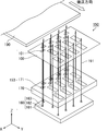
- FIG. 20 is a schematic perspective view of an organic EL element manufacturing apparatus according to Comparative Embodiment 1 examined by the present inventors.
- the organic EL element manufacturing apparatus according to Comparative Embodiment 1 is a vacuum vapor deposition apparatus that employs a scan film formation method, and is provided in a vapor deposition chamber (a vacuum chamber, not shown) and a vapor deposition chamber.
- the vapor deposition unit 1153 and a transport mechanism (not shown) for transporting the organic EL display device substrate 1190 to be vapor deposited are provided.
- the vapor deposition unit 1153 includes a plurality of vapor deposition sources 1160 provided with a plurality of nozzles 1162 and a plurality of vapor deposition sources 1160.
- a plurality of openings 1171 corresponding to the nozzles 1162 are formed, a limiting plate 1170 for defining a flight range of vapor deposition particles (vaporized material) emitted from the nozzles 1162, and a plurality of mask openings (through holes) for pattern formation
- an organic EL element manufacturing mask 1100 provided with a plurality of opening regions 1101 each including 1102. Then, vapor deposition particles are deposited on the substrate 1190 via the mask 1100 while the substrate 1190 is transported along the Y-axis direction above the mask 1100 by the transport mechanism.
- a hole transport layer is formed on the substrate 1190 so as to cover all pixels, and a light emitting layer material is used as an evaporation material. As a result, a light emitting layer is formed on the hole transport layer in a pattern following the pattern of the mask opening 1102, that is, in a stripe pattern.
- the adjacent opening regions 1101 are separated by the same width as the width of the opening region 1101 in the X-axis direction, a pattern cannot be formed over the entire region to be deposited only by transporting the substrate 1190 once. Therefore, in this comparative embodiment, after the substrate 1190 is transported once, the first light emitting layer pattern is formed in substantially half of the deposition region, and then each opening region 1101 is opposed to the region where the pattern is not formed. Then, the vapor deposition unit 1153 or the substrate 1190 is moved in the X-axis direction, and the substrate 1190 is transported again to form the second light emitting layer pattern on the remaining half of the deposition area.
- contamination generated from a member (for example, a transport mechanism) in the vapor deposition chamber. It will adhere to the surface.
- contamination the grease component which scattered from the member is mentioned, for example.
- the first light emitting layer pattern is formed, and after the deposition unit 1153 or the substrate 1190 is moved in the X-axis direction, the second light emitting layer pattern is formed. Therefore, the amount of contamination adhered to the region where the second light emitting layer pattern is formed is larger than the region where the first light emitting layer pattern is formed, and the luminance of the latter region is higher than that of the former region. It will be lower than the brightness. Then, the luminance difference between these two areas is observed as stitch unevenness. That is, it is considered that the cause of stitch unevenness is that the time difference between the two regions until the start of vapor deposition is large.
- T / S the directivity of the flow of vapor deposition particles (hereinafter also referred to as vapor deposition flow) is high, and the width of the vapor deposition flow is narrowed.
- the width of the vapor deposition flow is narrow, it is necessary to arrange the nozzles 1162 at a narrow pitch in order to form a pattern over the entire vapor deposition region of the substrate 1190 by one transport.
- the nozzles 1162 are arranged at a narrow pitch, the density of the vapor deposition particles increases in the vicinity of the nozzles 1162, and the scattering of the vapor deposition particles increases, resulting in problems such as blurring.
- the blur means a side portion of the formed film (deposited film) where the film thickness formed on both sides of the intermediate portion having a constant film thickness gradually decreases.
- FIG. 21 is a perspective plan view of the vapor deposition block as seen from the vapor deposition mask side in the organic EL element manufacturing apparatus described in Patent Document 2.
- FIG. 21 in the organic EL element manufacturing apparatus shown in FIG. 17 of Patent Document 2, a plurality of vapor deposition source openings 1261 formed in the vapor deposition source 1260 are arranged in a staggered pattern in two rows, and the X-axis direction A pair of limiting plates 1281 adjacent to each other, a single vapor deposition source opening 1261 disposed between the pair of limiting plates 1281, and a plurality of mask openings 1271 disposed between the pair of limiting plates 1281.
- a block 1251 is configured, and a plurality of vapor deposition blocks 1251 are arranged in a staggered manner. As a result, the degree of freedom in device design can be increased, and the light emitting layer pattern can be formed over the entire area to be deposited by transporting the substrate once.
- the region to be deposited by the second row deposition block 1251 is exposed to contamination, and this region is more exposed by the first row deposition block 1251. More contaminants will adhere than the area to be deposited. Therefore, the amount of contamination adhered to the region deposited by the deposition block 1251 in the second row is larger than the region deposited by the deposition block 1251 in the first row, and as a result, stitch unevenness is also caused. Will occur.
- the present invention has been made in view of the above situation, and is a mask for manufacturing an organic EL element, an organic EL element manufacturing apparatus, and an organic EL capable of reducing luminance unevenness and relaxing restrictions on the manufacturing apparatus.
- An object of the present invention is to provide a method for manufacturing an element.
- the organic electroluminescence element manufacturing mask includes a pattern forming portion provided with a plurality of mask openings for pattern formation,
- the pattern forming portion includes first to fourth opening regions arranged in a staggered manner, The first, second, third and fourth opening regions are arranged in this order along a first direction parallel to the pattern forming portion, The first opening region, the second opening region, the third opening region, and the fourth opening region are parallel to the pattern forming portion and in the first direction, respectively.
- a plurality of first mask openings, a plurality of second mask openings, a plurality of third mask openings, and a plurality of fourth mask openings are provided in a second direction orthogonal to each other,
- the plurality of third mask openings are arranged corresponding to the plurality of first mask openings, Each of the plurality of first mask openings and the third mask opening corresponding to the first mask opening are located on the same straight line parallel to the first direction
- the plurality of fourth mask openings are arranged corresponding to the plurality of second mask openings, Each of the plurality of second mask openings and the fourth mask opening corresponding to the second mask opening are located on the same straight line parallel to the first direction,
- No mask opening is provided on the opposite side of the first opening region from the third opening region,
- the lengths of each of the plurality of first mask openings and the plurality of second mask openings in the first direction are the plurality of third mask openings and the plurality of fourth masks. It may be a mask for manufacturing an organic electrolumin
- the organic electroluminescent element manufacturing apparatus includes a mask according to the present invention, and a vapor deposition unit including a vapor deposition source that emits vapor deposition particles, A transport mechanism for moving the substrate relative to the vapor deposition unit along the first direction in a state where the substrate is separated from the mask according to the present invention;
- the first, second, third, and fourth opening regions are opposed to the substrate in this order, or the fourth, third, second, and first opening regions.
- the organic electroluminescence element manufacturing apparatus may be arranged so as to face the substrate in this order.
- this organic EL element manufacturing apparatus is also referred to as a manufacturing apparatus according to the present invention.
- Still another embodiment of the present invention is a method for producing an organic electroluminescent element using a mask for producing an organic electroluminescent element
- the organic electroluminescence element manufacturing mask includes a pattern forming portion provided with a plurality of mask openings for pattern formation,
- the pattern forming portion includes first to fourth opening regions arranged in a staggered manner, The first, second, third and fourth opening regions are arranged in this order along a first direction parallel to the pattern forming portion, The first opening region, the second opening region, the third opening region, and the fourth opening region are parallel to the pattern forming portion and in the first direction, respectively.
- a plurality of first mask openings, a plurality of second mask openings, a plurality of third mask openings, and a plurality of fourth mask openings are provided in a second direction orthogonal to each other,
- the plurality of third mask openings are arranged corresponding to the plurality of first mask openings, Each of the plurality of first mask openings and the third mask opening corresponding to the first mask opening are located on the same straight line parallel to the first direction
- the plurality of fourth mask openings are arranged corresponding to the plurality of second mask openings, Each of the plurality of second mask openings and the fourth mask opening corresponding to the second mask opening are located on the same straight line parallel to the first direction,
- No mask opening is provided on the opposite side of the first opening region from the third opening region,
- the lengths of each of the plurality of first mask openings and the plurality of second mask openings in the first direction are the plurality of third mask openings and the plurality of fourth masks.
- the manufacturing method includes vapor deposition including the organic electroluminescence element manufacturing mask and a deposition source that emits vapor deposition particles along the first direction in a state where the substrate is separated from the organic electroluminescence element manufacturing mask.
- the organic electroluminescence element manufacturing mask is arranged such that the first, second, third, and fourth opening regions are opposed to the substrate in this order, or the fourth, third, It may be a method for manufacturing an organic electroluminescence element arranged so that the second and first opening regions are opposed to the substrate in this order.
- this method for producing an organic EL element is also referred to as a production method according to the present invention.
- the phrase “moving a certain object (for example, a substrate) along a certain direction (for example, the first direction)” refers not only to moving that object in that direction but also to that direction. This includes moving the object in the opposite direction. Therefore, for example, in the manufacturing apparatus according to the present invention, the substrate may be moved relative to the vapor deposition unit in the first direction by the transport mechanism, or opposite to the first direction. It may be moved relative to the vapor deposition unit in the direction of.
- the lengths of the plurality of first mask openings in the first direction and the lengths of the plurality of second mask openings in the first direction may be substantially the same.
- the pattern forming unit further includes fifth and sixth opening regions, The first to sixth opening regions are arranged in a staggered manner, The first, second, fifth, sixth, third and fourth opening regions are arranged in this order along the first direction, Each of the fifth opening region and the sixth opening region is provided with a plurality of fifth mask openings and a plurality of sixth mask openings in the second direction.
- the plurality of fifth mask openings are arranged corresponding to the plurality of first mask openings and the plurality of third mask openings, Each of the plurality of first mask openings and the fifth mask opening and the third mask opening corresponding to the first mask opening are on the same straight line parallel to the first direction.
- the plurality of sixth mask openings are arranged corresponding to the plurality of second mask openings and the plurality of fourth mask openings, Each of the plurality of second mask openings and the sixth mask opening and the fourth mask opening corresponding to the second mask opening are on the same straight line parallel to the first direction.
- Position to, The length of each of the plurality of fifth mask openings and the plurality of sixth mask openings in the first direction is equal to the plurality of third mask openings and the plurality of fourth masks. Each of the openings may be shorter than the length in the first direction.
- the pattern forming unit further includes fifth and sixth opening regions, The first to sixth opening regions are arranged in a staggered manner, The first, second, third, fourth, fifth and sixth opening regions are arranged in this order along the first direction, Each of the fifth opening region and the sixth opening region is provided with a plurality of fifth mask openings and a plurality of sixth mask openings in the second direction.
- the plurality of fifth mask openings are arranged corresponding to the plurality of first mask openings and the plurality of third mask openings, Each of the plurality of first mask openings and the fifth mask opening and the third mask opening corresponding to the first mask opening are on the same straight line parallel to the first direction.
- the plurality of sixth mask openings are arranged corresponding to the plurality of second mask openings and the plurality of fourth mask openings, Each of the plurality of second mask openings and the sixth mask opening and the fourth mask opening corresponding to the second mask opening are on the same straight line parallel to the first direction.
- Position to, The length of each of the plurality of fifth mask openings and the plurality of sixth mask openings in the first direction is equal to the plurality of third mask openings and the plurality of fourth masks. Each of the openings may be shorter than the length in the first direction.
- the lengths of the plurality of fifth mask openings in the first direction and the lengths of the plurality of sixth mask openings in the first direction may be substantially the same.
- the vapor deposition source may be provided with first, second, third and fourth outlets corresponding to the first, second, third and fourth opening regions, respectively.
- the vapor deposition source may be provided with a first injection port corresponding to the first and third opening regions and a second injection port corresponding to the second and fourth opening regions.
- the first injection port when viewed along the first direction and a third direction orthogonal to the second direction, the center of the first opening region, and the third Placed in the center between the center of the opening area of The second injection port is disposed at the center between the center portion of the second opening region and the center portion of the fourth opening region when viewed along the third direction. Also good.
- the manufacturing apparatus according to the present invention further comprises a mask according to the present invention, and a limiting plate provided between the vapor deposition sources,
- the restriction plate may be provided with first, second, third, and fourth openings corresponding to the first, second, third, and fourth opening regions, respectively.
- a limiting plate provided with first, second, third, and fourth openings corresponding to the first, second, third, and fourth opening regions, respectively, is provided with the organic electroluminescence. You may arrange
- the manufacturing apparatus according to the present invention further includes a mask according to the present invention, and a plurality of additional restriction plates provided between the restriction plates,
- the plurality of additional limiting plates are divided into four spaces corresponding to the first, second, third, and fourth opening regions, respectively, by partitioning a space between the mask according to the present invention and the limiting plate. Also good.
- the space between the organic electroluminescence element manufacturing mask and the restriction plate is partitioned to be divided into four spaces corresponding to the first, second, third, and fourth opening regions, respectively.
- a plurality of additional restriction plates may be disposed between the organic electroluminescence element manufacturing mask and the restriction plate.
- an organic EL element manufacturing mask it is possible to realize an organic EL element manufacturing mask, an organic EL element manufacturing apparatus, and an organic EL element manufacturing method capable of reducing luminance unevenness and relaxing restrictions on a manufacturing apparatus. it can.
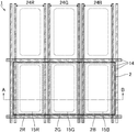
- FIG. 2 is a schematic plan view illustrating a configuration in a display region of the organic EL display device illustrated in FIG. 1.
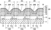
- FIG. 3 is a schematic cross-sectional view showing a configuration of a TFT substrate of the organic EL display device shown in FIG. 1, and corresponds to a cross section taken along line AB in FIG. 5 is a flowchart for explaining a manufacturing process of the organic EL element and the organic EL display device according to the first embodiment.
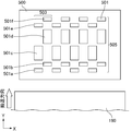
- 2 is a schematic plan view of an organic EL element manufacturing mask according to Embodiment 1.
- FIG. FIG. 1 is a schematic plan view of an organic EL element manufacturing mask according to Embodiment 1.
- FIG. 3 is a schematic plan view of an organic EL element manufacturing mask according to Embodiment 1, and shows an enlarged opening block.
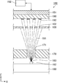
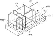
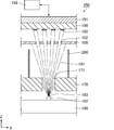
- 1 is a schematic perspective view of an organic EL element manufacturing apparatus according to Embodiment 1.
- FIG. 1 is a schematic plan view of an organic EL element manufacturing apparatus according to Embodiment 1.
- FIG. It is a cross-sectional schematic diagram of the organic EL element manufacturing apparatus according to Embodiment 1, and shows a cross section perpendicular to the Y-axis direction.
- FIG. 6 is a schematic plan view of an organic EL element manufacturing apparatus according to Embodiment 2.
- 5 is a schematic perspective view of an organic EL element manufacturing apparatus according to Embodiment 2.
- FIG. 6 is a schematic perspective view of an organic EL element manufacturing apparatus according to Embodiment 3.
- FIG. 6 is a schematic plan view of an organic EL element manufacturing apparatus according to Embodiment 3.
- FIG. 6 is a schematic plan view of an organic EL element manufacturing mask according to Embodiment 4.
- FIG. 10 is a schematic plan view of an organic EL element manufacturing mask according to Embodiment 4 and shows an enlarged opening block.
- 6 is a schematic plan view of an organic EL element manufacturing mask according to Embodiment 5.
- FIG. 10 is a schematic plan view of an organic EL element manufacturing mask according to Embodiment 5 and shows an enlarged opening block.
- 10 is a schematic plan view of an organic EL element manufacturing mask according to Embodiment 6.
- FIG. It is a perspective schematic diagram of the manufacturing apparatus of the organic EL element which concerns on the comparison form 1 which the present inventors examined. In the manufacturing apparatus of the organic EL element of patent document 2, it is the perspective top view seen from the vapor deposition mask side of the vapor deposition block. It is a plane schematic diagram of the organic EL element manufacturing mask which concerns on the comparative form 2 which the present inventors examined.
- the X-axis direction, the Y-axis direction, and the Z-axis direction are respectively the second direction, the first direction, and the mask according to the present invention and the manufacturing apparatus according to the present invention. And corresponds to the third direction.
- Embodiment 1 a bottom emission type organic EL element manufacturing apparatus and manufacturing method for an organic EL display device for RGB full color display that extracts light from the TFT substrate side, and an organic EL element manufactured by the manufacturing apparatus or manufacturing method thereof
- this embodiment can also be applied to methods for manufacturing other types of organic EL elements.
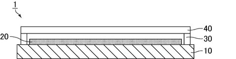
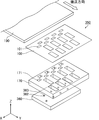
- FIG. 1 is a schematic cross-sectional view of an organic EL display device including an organic EL element manufactured by the method for manufacturing an organic EL element according to Embodiment 1.
- FIG. 2 is a schematic plan view showing a configuration in the display area of the organic EL display device shown in FIG. 3 is a schematic cross-sectional view showing the configuration of the TFT substrate of the organic EL display device shown in FIG. 1, and shows a cross section taken along the line AB in FIG.
- the organic EL display device 1 includes a TFT substrate 10 provided with a TFT 12 (see FIG. 3), and an organic EL element provided on the TFT substrate 10 and connected to the TFT 12. 20, an adhesive layer 30 provided in a frame shape so as to surround the organic EL element 20, and a sealing substrate 40 disposed so as to cover the organic EL element 20.
- the adhesive layer 30 bonds the peripheral edge of the TFT substrate 10 and the peripheral edge of the sealing substrate 40 together.
- the organic EL element 20 is sealed between the pair of substrates 10 and 40 by bonding the sealing substrate 40 and the TFT substrate 10 on which the organic EL element 20 is laminated using the adhesive layer 30. . This prevents oxygen and moisture from entering the organic EL element 20 from the outside.
- the TFT substrate 10 has a transparent insulating substrate 11 such as a glass substrate as a support substrate.
- a plurality of wirings 14 are formed on the insulating substrate 11, and the plurality of wirings 14 includes a plurality of gate lines provided in a horizontal (vertical) direction and a vertical (lateral) direction. And a plurality of signal lines intersecting with the gate lines.
- a gate line driving circuit (not shown) for driving the gate line is connected to the gate line
- a signal line driving circuit (not shown) for driving the signal line is connected to the signal line.
- the organic EL display device 1 is an active matrix display device for RGB full-color display, and each region partitioned by the wiring 14 has red (R), green (G), or blue (B) sub-pixels (dots). ) 2R, 2G or 2B is arranged. The subpixels 2R, 2G, and 2B are arranged in a matrix. Corresponding color organic EL elements 20 and light emitting regions are formed in the sub-pixels 2R, 2G, and 2B of the respective colors.
- the red, green, and blue sub-pixels 2R, 2G, and 2B emit light with red light, green light, and blue light, respectively, and one pixel 2 is configured from the three sub-pixels 2R, 2G, and 2B. Yes.
- the sub-pixels 2R, 2G, and 2B are provided with openings 15R, 15G, and 15B, respectively, and the openings 15R, 15G, and 15B are formed by red, green, and blue light emitting layers 24R, 24G, and 24B, respectively. Covered.
- the light emitting layers 24R, 24G, and 24B are formed in stripes in the vertical (longitudinal) direction.
- the patterns of the light emitting layers 24R, 24G, and 24B are formed by vapor deposition for each color.
- the openings 15R, 15G, and 15B will be described later.
- Each subpixel 2R, 2G, 2B is provided with a TFT 12 connected to the first electrode 21 of the organic EL element 20.
- the light emission intensity of each of the sub-pixels 2R, 2G, and 2B is determined by scanning and selection by the wiring 14 and the TFT 12.
- the organic EL display device 1 realizes image display by selectively emitting the organic EL elements 20 of each color with desired luminance using the TFT 12.
- the configuration of the TFT substrate 10 and the organic EL element 20 will be described in detail. First, the TFT substrate 10 will be described.
- the TFT substrate 10 includes a TFT 12 (switching element) and a wiring 14 formed on the insulating substrate 11, an interlayer film (interlayer insulating film, planarizing film) 13 covering them, and an interlayer film 13. And an edge cover 15 which is an insulating layer formed thereon.
- the TFT 12 is provided corresponding to each sub-pixel 2R, 2G, 2B.
- illustration and description of each layer in TFT12 are abbreviate
- the interlayer film 13 is formed on the insulating substrate 11 over the entire region of the insulating substrate 11.
- a first electrode 21 of the organic EL element 20 is formed on the interlayer film 13.
- the interlayer film 13 is provided with a contact hole 13 a for electrically connecting the first electrode 21 to the TFT 12. Thereby, the TFT 12 is electrically connected to the organic EL element 20 through the contact hole 13a.
- the edge cover 15 prevents the first electrode 21 and the second electrode 27 of the organic EL element 20 from being short-circuited due to a thin organic EL layer or an electric field concentration at the end of the first electrode 21. Is formed for. Therefore, the edge cover 15 is formed so as to partially cover the end portion of the first electrode 21.
- the edge cover 15 is provided with the above-described openings 15R, 15G, and 15B.
- Each opening 15R, 15G, 15B of the edge cover 15 becomes a light emitting region of the sub-pixels 2R, 2G, 2B.
- the sub-pixels 2R, 2G, and 2B are partitioned by the edge cover 15 having an insulating property.
- the edge cover 15 also functions as an element isolation film.
- the organic EL element 20 is a light emitting element that can emit light with high luminance by direct current drive, and includes a first electrode 21, an organic EL layer, and a second electrode 27, which are stacked in this order.
- the first electrode 21 is a layer having a function of injecting (supplying) holes into the organic EL layer.
- the first electrode 21 is connected to the TFT 12 through the contact hole 13a as described above.
- a hole injection layer 22 As an organic EL layer, from the first electrode 21 side, a hole injection layer 22, a hole transport layer 23, a light emitting layer 24R, 24G or 24B, the electron transport layer 25, and the electron injection layer 26 are laminated in this order.
- the order of lamination is that when the first electrode 21 is an anode and the second electrode 27 is a cathode, and when the first electrode 21 is a cathode and the second electrode 27 is an anode, the organic layer is organic.
- the stacking order of the EL layers is reversed.
- the hole injection layer 22 is a layer having a function of increasing the efficiency of hole injection into each of the light emitting layers 24R, 24G, and 24B.
- the hole transport layer 23 is a layer having a function of increasing the hole transport efficiency to each of the light emitting layers 24R, 24G, and 24B.
- the hole injection layer 22 is uniformly formed on the entire display region of the TFT substrate 10 so as to cover the first electrode 21 and the edge cover 15.
- the hole transport layer 23 is uniformly formed on the entire display region of the TFT substrate 10 so as to cover the hole injection layer 22.
- the hole injection layer 22 and the hole transport layer 23 may be formed as independent layers as described above, or may be provided integrally with each other. That is, the organic EL display device 1 may include a hole injection / hole transport layer instead of the hole injection layer 22 and the hole transport layer 23.
- the hole injection / hole transport layer is a layer having both the function of the hole injection layer and the function of the hole transport layer.
- light emitting layers 24R, 24G and 24B are formed corresponding to the sub-pixels 2R, 2G and 2B so as to cover the openings 15R, 15G and 15B of the edge cover 15, respectively. Yes.
- Each of the light emitting layers 24R, 24G, and 24B is a layer having a function of emitting light by recombining holes injected from the first electrode 21 side and electrons injected from the second electrode 27 side. is there.
- Each of the light emitting layers 24R, 24G, and 24B is formed of a material having high light emission efficiency, such as a low molecular fluorescent dye or a metal complex.
- the electron transport layer 25 is a layer having a function of increasing the electron transport efficiency from the second electrode 27 to each of the light emitting layers 24R, 24G, and 24B.
- the electron injection layer 26 is a layer having a function of increasing the efficiency of electron injection from the second electrode 27 to each of the light emitting layers 24R, 24G, and 24B.
- the electron transport layer 25 is uniformly formed on the entire display region of the TFT substrate 10 so as to cover the light emitting layers 24R, 24G and 24B and the hole transport layer 23.
- the electron injection layer 26 is uniformly formed on the entire display region of the TFT substrate 10 so as to cover the electron transport layer 25.
- the electron transport layer 25 and the electron injection layer 26 may be formed as independent layers as described above, or may be provided integrally with each other. That is, the organic EL display device 1 may include an electron transport / electron injection layer instead of the electron transport layer 25 and the electron injection layer 26.
- the electron transport / electron injection layer is a layer having both the function of the electron injection layer and the function of the electron transport layer.
- the second electrode 27 is a layer having a function of injecting electrons into the organic EL layer.
- the second electrode 27 is uniformly formed on the entire display region of the TFT substrate 10 so as to cover the electron injection layer 26.
- the organic layers other than the light emitting layers 24R, 24G, and 24B are not essential layers as the organic EL layer, and can be appropriately formed according to the required characteristics of the organic EL element 20.
- a carrier blocking layer can also be added to the organic EL layer as necessary.
- a hole blocking layer may be added as a carrier blocking layer between the light emitting layers 24R, 24G, and 24B and the electron transport layer 25, thereby preventing holes from reaching the electron transport layer 25. , Luminous efficiency can be improved.
- first electrode / positive Hole injection layer / hole transport layer / electron injection layer / electron injection layer / electron injection layer / electron injection layer / second electrode (2) First electrode / hole transport layer / light emitting layer / electron transport layer / second electrode (3) First electrode / hole transport layer / light emitting layer / Hole blocking layer / electron transport layer / second electrode (4) first electrode / hole transport layer / light emitting layer / hole blocking layer / electron transport layer / electron injection layer / second electrode (5) first electrode / Hole injection layer / hole transport layer / light emitting layer / electron transport layer / electron injection layer / second electrode (6) first electrode / hole injection layer / hole transport layer / light emitting layer / hole blocking layer / electron Transport layer / second electrode (7) first electrode / hole injection layer / hole transport layer / light emitting layer / hole blocking layer / electron transport layer / electron injection layer / second electrode (8) first electrode / positive Hole injection layer / hole transport layer / electron transport layer
- the configuration of the organic EL element 20 is not particularly limited to the layer configurations of the above (1) to (8), and a desired layer configuration can be adopted according to the required characteristics of the organic EL element 20.
- FIG. 4 is a flowchart for explaining a manufacturing process of the organic EL element and the organic EL display device according to the first embodiment.
- the manufacturing method of the organic EL element and the organic EL display device includes, for example, a TFT substrate / first electrode manufacturing step S1, a hole injection layer deposition step S2, a hole transport layer. It includes a vapor deposition step S3, a light emitting layer vapor deposition step S4, an electron transport layer vapor deposition step S5, an electron injection layer vapor deposition step S6, a second electrode vapor deposition step S7, and a sealing step S8.
- the light emitting layer deposition step S4 is usually performed in an in-line manner, but may be performed in a single wafer manner. Other vapor deposition processes may be performed by an in-line method or a single wafer method.
- the stacking order described in the present embodiment is a case where the first electrode 21 is an anode and the second electrode 27 is a cathode, and conversely, the first electrode 21 is a cathode,
- the electrode 27 is used as an anode, the stacking order of the organic EL layers is reversed.
- the materials constituting the first electrode 21 and the second electrode 27 are also reversed.
- a photosensitive resin is applied on the insulating substrate 11 on which the TFTs 12, the wirings 14 and the like are formed by a general method, and patterning is performed on the insulating substrate 11 by photolithography.
- An interlayer film 13 is formed.
- the thickness is 0.7 to 1.1 mm
- the length in the Y-axis direction is 400 to 500 mm
- the length in the X-axis direction is 300.
- Examples include a glass substrate or a plastic substrate of ⁇ 400 mm.
- a resin such as an acrylic resin or a polyimide resin can be used as a material of the interlayer film 13.
- the acrylic resin include Optomer series manufactured by JSR Corporation.
- a polyimide resin the photo nice series by Toray Industries, Inc. is mentioned, for example.
- the polyimide resin is generally not transparent but colored. Therefore, when a bottom emission type organic EL display device is manufactured as the organic EL display device 1 as shown in FIG. 3, a transparent resin such as an acrylic resin is more preferably used as the interlayer film 13. .
- the film thickness of the interlayer film 13 is not particularly limited as long as the step due to the TFT 12 is filled and the surface of the interlayer film 13 becomes flat. For example, it may be approximately 2 ⁇ m.
- a contact hole 13 a for electrically connecting the first electrode 21 to the TFT 12 is formed in the interlayer film 13.
- a conductive film for example, an ITO (Indium Tin Oxide) film is formed to a thickness of 100 nm by a sputtering method or the like.
- ITO Indium Tin Oxide
- the ITO film is etched using ferric chloride as an etchant. Thereafter, the photoresist is stripped using a resist stripping solution, and substrate cleaning is further performed. As a result, the first electrodes 21 are formed in a matrix on the interlayer film 13.
- Examples of the conductive film material used for the first electrode 21 include transparent conductive materials such as ITO, IZO (Indium Zinc Oxide), and gallium-doped zinc oxide (GZO); gold (Au), nickel Metal materials such as (Ni) and platinum (Pt) can be used.
- transparent conductive materials such as ITO, IZO (Indium Zinc Oxide), and gallium-doped zinc oxide (GZO); gold (Au), nickel Metal materials such as (Ni) and platinum (Pt) can be used.
- a vacuum deposition method As a method for laminating the conductive film, in addition to the sputtering method, a vacuum deposition method, a CVD (Chemical Vapor Deposition) method, a plasma CVD method, a printing method, or the like can be used.
- a vacuum deposition method As a method for laminating the conductive film, in addition to the sputtering method, a vacuum deposition method, a CVD (Chemical Vapor Deposition) method, a plasma CVD method, a printing method, or the like can be used.
- CVD Chemical Vapor Deposition
- the thickness of the 1st electrode 21 is not specifically limited, As above-mentioned, it can be 100 nm, for example.
- the edge cover 15 is formed with a film thickness of, for example, approximately 1 ⁇ m by the same method as the interlayer film 13.
- the same insulating material as that of the interlayer film 13 can be used.
- the TFT substrate 10 and the first electrode 21 are manufactured (S1).
- the TFT substrate 10 that has undergone the above steps is subjected to reduced pressure baking for dehydration and oxygen plasma treatment for cleaning the surface of the first electrode 21.
- the hole injection layer 22 is deposited on the entire surface of the display area of the TFT substrate 10 on the TFT substrate 10 using a general vacuum deposition apparatus (S2).
- an open mask having an opening corresponding to the entire surface of the display area is adhered and bonded to the TFT substrate 10 after alignment adjustment. Then, while rotating the TFT substrate 10 and the open mask together, the vapor deposition particles scattered from the vapor deposition source are uniformly vapor deposited on the entire display area through the opening of the open mask.
- vapor deposition on the entire surface of the display region means vapor deposition without interruption between adjacent sub-pixels of different colors.
- the hole transport layer 23 is deposited on the entire display region of the TFT substrate 10 so as to cover the hole injection layer 22 (S3).
- the material of the hole injection layer 22 and the hole transport layer 23 is not particularly limited.
- the hole injection layer 22 and the hole transport layer 23 may be integrated as described above, or may be formed as independent layers.
- Each film thickness is, for example, 10 to 100 nm.
- a hole injection / hole transport layer is formed as the hole injection layer 22 and the hole transport layer 23
- a material of the hole injection / hole transport layer for example, 4,4′-bis [N- (1- Naphthyl) -N-phenylamino] biphenyl ( ⁇ -NPD) can be used.
- the film thickness of a positive hole injection and positive hole transport layer can be 30 nm, for example.
- light emitting layers 24R, 24G, and 24B are separately formed on the hole transport layer 23 so as to cover the openings 15R, 15G, and 15B of the edge cover 15 and corresponding to the sub-pixels 2R, 2G, and 2B. (Pattern formation) is performed (S4).
- a material having high light emission efficiency such as a low molecular fluorescent dye or a metal complex is used.
- the material of the light emitting layers 24R, 24G, and 24B is not particularly limited.
- each light emitting layer 24R, 24G, 24B is, for example, 10 to 100 nm.
- the manufacturing method and the manufacturing apparatus according to the present invention can be particularly preferably used for forming such light emitting layers 24R, 24G, and 24B.
- the electron transport layer 25 is deposited on the entire display region of the TFT substrate 10 so as to cover the hole transport layer 23 and the light emitting layers 24R, 24G, and 24B by the same method as in the hole injection layer deposition step S2. (S5).
- the electron injection layer 26 is deposited on the entire display region of the TFT substrate 10 so as to cover the electron transport layer 25 by the same method as in the hole injection layer deposition step S2 (S6).
- the material for the electron transport layer 25 and the electron injection layer 26 is not particularly limited.
- Alq3 tris (8-hydroxyquinoline) aluminum
- anthracene naphthalene
- phenanthrene pyrene
- anthracene perylene
- butadiene coumarin
- acridine stilbene
- 1,10-phenanthroline and derivatives thereof Metal complex
- LiF LiF
- the electron transport layer 25 and the electron injection layer 26 may be integrated or formed as independent layers.
- Each film thickness is, for example, 1 to 100 nm, preferably 10 to 100 nm.
- the total film thickness of the electron transport layer 25 and the electron injection layer 26 is, for example, 20 to 200 nm.
- the electron transport layer 25 has a thickness of 30 nm
- the electron injection layer 26 has a thickness of 1 nm.
- the second electrode 27 is deposited on the entire display region of the TFT substrate 10 so as to cover the electron injection layer 26 by the same method as in the hole injection layer deposition step S2 (S7).
- the organic EL element 20 including the organic EL layer, the first electrode 21 and the second electrode 27 is formed on the TFT substrate 10.
- Electrode material of the second electrode 27 a metal having a small work function is preferably used.
- examples of such electrode materials include magnesium alloys (MgAg, etc.), aluminum alloys (AlLi, AlCa, AlMg, etc.), metallic calcium, and the like.
- the thickness of the second electrode 27 is, for example, 50 to 100 nm.
- the second electrode 27 is formed from an aluminum thin film having a thickness of 50 nm.
- the TFT substrate 10 on which the organic EL element 20 is formed and the sealing substrate 40 are bonded together using the adhesive layer 30, and the organic EL element 20 is sealed (S8). .
- sealing resin for example, sealing resin, frit glass, or the like can be used.
- sealing substrate 40 for example, an insulating substrate such as a glass substrate or a plastic substrate having a thickness of 0.4 to 1.1 mm is used. Further, an engraved glass may be used as the sealing substrate 40.
- the vertical length and the horizontal length of the sealing substrate 40 may be appropriately adjusted according to the size of the target organic EL display device 1, and an insulating substrate having substantially the same size as the insulating substrate 11 of the TFT substrate 10 is used. After sealing the organic EL element 20, the organic EL element 20 may be divided according to the size of the target organic EL display device 1.
- the sealing method of the organic EL element 20 is not particularly limited to the above-described method, and any other sealing method can be employed. Examples of other sealing methods include a method of filling a resin between the TFT substrate 10 and the sealing substrate 40.
- a protective film (not shown) is provided on the second electrode 27 so as to cover the second electrode 27 and prevent oxygen and moisture from entering the organic EL element 20 from the outside. It may be.
- the protective film can be formed of an insulating or conductive material. Examples of such a material include silicon nitride and silicon oxide.
- the thickness of the protective film is, for example, 100 to 1000 nm.
- the organic EL display device 1 is completed.
- the organic EL display device 1 when the TFT 12 is turned on by signal input from the wiring 14, holes are injected from the first electrode 21 to the organic EL layer. On the other hand, electrons are injected from the second electrode 27 into the organic EL layer, and holes and electrons are recombined in each of the light emitting layers 24R, 24G, and 24B.
- the light emitting material is excited by the energy of recombination of holes and electrons, and light is emitted when the excited state returns to the ground state.
- a predetermined image is displayed by controlling the light emission luminance of each of the sub-pixels 2R, 2G, and 2B.
- the organic EL element manufacturing mask according to the present embodiment performs vapor deposition while moving the substrate relative to the vapor deposition unit including the mask and the vapor deposition source in this order from the substrate side. It is used for an EL element manufacturing apparatus and manufacturing method. First, the organic EL element manufacturing mask according to the present embodiment will be described in detail, and the manufacturing apparatus and manufacturing method (particularly, the light emitting layer deposition step S4) according to the present embodiment will be described later.
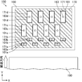
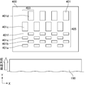
- FIG. 5 is a schematic plan view of the organic EL element manufacturing mask according to the first embodiment.
- the organic EL element manufacturing mask 100 according to the present embodiment is a flat plate member, and includes a thin flat plate pattern forming portion 105 in which an opening pattern is formed.
- the pattern forming unit 105 is provided with a plurality of opening regions 101 each having a plurality of mask openings for pattern formation (through holes, not shown in FIG. 5).
- the plurality of opening regions 101 are arranged in a staggered manner in four rows and eight rows.
- both the Y-axis direction and the X-axis direction are set to be parallel to the pattern forming unit 105.
- the number of columns in the vertical direction (Y-axis direction) of the opening region 101 is four, but the number of columns in the horizontal direction (X-axis direction) of the opening region 101 is two or more. If it is, it will not specifically limit, It can increase / decrease suitably according to the length of the X-axis direction of the vapor deposition area
- the plurality of opening regions 101 includes a first opening region 101a, a second opening region 101b, a third opening region 101c, and a fourth opening region 101d arranged in a staggered manner, and the opening region 101a , 101b, 101c and 101d are alternately arranged in this order in the Y-axis direction.
- the opening areas 101a and 101c are arranged at the same position in the X-axis direction, and the opening areas 101b and 101d are arranged at the same position in the X-axis direction, but the Y of the opening areas 101a, 101b, 101c and 101d
- the positions in the axial direction are different from each other, and the opening regions 101a, 101b, 101c, and 101d do not overlap in the Y-axis direction.
- the opening region 101a is located at the extreme end in the Y-axis direction, and on the opposite side of the opening region 101c to the opening region 101c, that is, the opening region 101a and the mask 100 adjacent to the opening region 101a in the Y-axis direction. No other mask opening for pattern formation is formed between the end 104. Further, no other mask opening for pattern formation is formed on the opposite side of the opening region 101 b from the opening region 101 d, that is, between the opening region 101 b and the end portion 104.
- the mask 100 includes a plurality of opening blocks 103 including first to fourth opening regions 101a to 101d, and the plurality of opening blocks 103 are arranged at an equal pitch in the X-axis direction. , Including the same configuration, ie, the same opening pattern.
- a device for manufacturing an organic EL element including the mask 100 (a device for manufacturing an organic EL element according to this embodiment to be described later), a light emitting layer deposition step S4 using the mask 100 (a method for manufacturing an organic EL element according to this embodiment), Then, the substrate 190 is moved relative to the mask 100 at a constant speed in the Y-axis direction so as to face the first, second, third, and fourth opening regions 101a, 101b, 101c, and 101d in this order. While transporting (moving), the light emitting material is deposited on the substrate 190.
- vapor deposition particles (vaporized material) are deposited on the substrate 190 through the plurality of mask openings in the first opening region 101a, and then through the plurality of mask openings in the second opening region 101b.
- the deposited particles are deposited on the substrate 190, and then the deposited particles are deposited on the substrate 190 through the plurality of mask openings in the third opening region 101c, and finally the plurality of masks in the fourth opening region 101d.
- the vapor deposition particles are vapor-deposited on the substrate 190 through the opening.
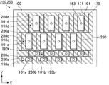
- FIG. 6 is a schematic plan view of the organic EL element manufacturing mask according to the first embodiment, and shows one enlarged opening block.
- a plurality of mask openings (through holes) 102 are provided in each opening region 101.
- 102a, 102b, 102c and 102d are provided in the first, second, third and fourth mask openings arranged in the X-axis direction, respectively.
- 102a, 102b, 102c and 102d are provided.
- Each mask opening 102a, 102b, 102c, 102d has a longitudinal shape in a plan view (when viewed along the Z-axis direction), and is disposed along the Y-axis direction.
- the third mask opening 102c has a one-to-one correspondence with the first mask opening 102a, and each mask opening 102c is disposed at the same position as the corresponding mask opening 102a in the X-axis direction.
- the mask opening 102c and the corresponding mask opening 102a are arranged on the same straight line 120a parallel to the Y-axis direction. Accordingly, when the substrate (not shown in FIG. 6) is moved relative to the mask 100 in the Y-axis direction, the mask opening 102c is formed in the region (subpixel) where the vapor deposition material is deposited through the mask opening 102a. Then, the vapor deposition material is again vapor-deposited.
- the fourth mask opening 102d has a one-to-one correspondence with the second mask opening 102b, and each mask opening 102d is disposed at the same position as the corresponding mask opening 102b in the X-axis direction.
- Each mask opening 102d and the corresponding mask opening 102b are arranged on the same straight line 120b parallel to the Y-axis direction. Accordingly, when the substrate is moved relative to the mask 100 in the Y-axis direction, the deposition material is again deposited through the mask opening 102d in the region (sub-pixel) where the deposition material is deposited through the mask opening 102b. Will be.
- the mask opening group including all the first mask openings 102a and all the second mask openings 102b is arranged at an equal pitch in the X-axis direction, and the pitch is equal to the pixel pitch in the X-axis direction.
- a group of mask openings including all the third mask openings 102c and all the fourth mask openings 102d are arranged at an equal pitch in the X-axis direction, and the pitch is a pixel pitch in the X-axis direction. Is set to the same.
- a stripe pattern is formed as the light emitting layer 24R, 24G, or 24B over the entire deposition area of the substrate only by moving the substrate relative to the mask 100 once in the Y-axis direction. be able to.
- the major feature of this embodiment is that the length of each of the mask openings on the upstream side facing the substrate, that is, the lengths of the first and second mask openings 102a and 102b in the Y-axis direction are all masks.
- the shortest of the openings 102 is set to be shorter than the lengths of the third and fourth mask openings 102c and 102d in the Y-axis direction.
- the region deposited through the fourth mask opening 102d is in the deposition chamber while the deposition through the third mask opening 102c is performed. Will be exposed to contamination. The longer the deposition time through the third mask opening 102c, the thicker the contamination layer formed on the hole transport layer 23 in the region deposited through the fourth mask opening 102d. And the decrease in luminance becomes more prominent.
- the stitch unevenness can be suppressed by reducing the amount of contamination adhering immediately above the hole transport layer and providing an extremely thin light emitting layer thereon.
- the lengths of the first and second mask openings 102a and 102b on the upstream side are shortened.
- the vapor deposition through the second mask opening 102b can be performed for a short time immediately after the vapor deposition through the first mask opening 102a is started. Therefore, not only in the region deposited through the first and third mask openings 102a and 102c, but also in the region deposited through the second and fourth mask openings 102b and 102d, the hole transport layer.
- the contamination layer formed immediately above 23 can be made extremely thin, and an extremely thin light-emitting layer can be formed on the extremely thin contamination layer. Therefore, it is possible to suppress a decrease in luminance in the region deposited through the second and fourth mask openings 102b and 102d.
- the reason why the decrease in luminance is suppressed is that, firstly, since the amount of contamination immediately above the hole transport layer 23 is small, that is, the resistance component is small, the decrease in the injection efficiency of holes into the light emitting layer is suppressed. Secondly, the presence of an extremely thin light-emitting layer facilitates hole hopping movement.
- the light emitting layer pattern is not formed until the deposition is completed through the third mask opening 102c. . That is, in the region deposited through the first and third mask openings 102a and 102c, the ultrathin first contamination layer, the ultrathin light emitting layer, and the second on the hole transport layer 23. And a normal light emitting layer having a desired thickness (that is, the light emitting layer 24R, 24G, or 24B) are stacked in this order, and are deposited through the second and fourth mask openings 102b and 102d.
- an ultrathin third contamination layer, an ultrathin light emitting layer, a fourth contamination layer, and a normal light emitting layer having a desired thickness are stacked in this order, and the fourth contamination layer is expected to be thicker than the second contamination layer.
- the third contamination layer is extremely thin, holes injected from the hole transport layer 23 into the third contamination layer can be injected into the ultrathin light emitting layer with almost no decrease in injection efficiency.
- the holes are hopped through the ultrathin light-emitting layer and the fourth contamination layer and injected into a normal light-emitting layer having a desired thickness, where they recombine with electrons to form excitons and emit light. Will occur. That is, the presence of an extremely thin light emitting layer having the same energy level as that of a normal light emitting layer facilitates hopping movement of holes, and holes can be efficiently injected into a normal light emitting layer having a desired thickness.
- the holes injected from the hole transport layer 23 into the first contamination layer are very similar to the first contamination layer. Since it is thin, it is injected into a very thin light-emitting layer without reducing the injection efficiency, and the hole is hopped through the ultra-thin light-emitting layer and the second contamination layer and has a desired thickness. Where they recombine with electrons to form excitons and emit light.
- the hole transport layer is a layer adjacent to the light emitting layer 24R, 24G, or 24B.
- a hole injection layer or an electron blocking layer is formed instead of 23.
- stitch unevenness can be suppressed by the same principle.
- the hole injection layer, the hole transport layer, or the electron blocking layer is also collectively referred to as a hole injection / transport layer.
- the thickness of each of the ultra-thin light emitting layers is not particularly limited as long as it causes a hopping movement of holes. However, the thickness is preferably 10% or less with respect to the thickness of a normal light emitting layer. It is more preferable that If the ultrathin light emitting layer is too thick, the third contamination layer formed on the hole injection / transport layer in the region deposited through the second and fourth mask openings 102b and 102d becomes thick, There is a possibility that the decrease in luminance in the region becomes large. On the contrary, if the extremely thin light emitting layer is too thin, it is formed in an island shape, and the holes cannot be efficiently hopped. Therefore, the thickness of each ultrathin light emitting layer is preferably 1 nm (10 cm) or more.
- the length of each of the first and second mask openings 102a and 102b in the Y-axis direction is not particularly limited as long as hopping movement of holes occurs through the ultrathin light emitting layer formed by the first and second mask openings 102a and 102b. It is preferable that the thickness of each of the light emitting layers is set so as to be the above preferable thickness. Therefore, the length of each mask opening 102a is preferably 10% or less, more preferably 5% or less, of the length of the third mask opening 102c corresponding to the mask opening 102a. The length of each mask opening 102a is preferably set so that the film thickness of the ultrathin light emitting layer formed by the mask opening 102a is 1 nm or more.
- each mask opening 102b is preferably 10% or less, more preferably 5% or less, of the length of the fourth mask opening 102d corresponding to the mask opening 102b.
- the length of each mask opening 102b is preferably set so that the thickness of the ultrathin light emitting layer formed by the mask opening 102b is 1 nm or more.
- the preferred lower limit of the length of each mask opening 102a, 102b is easily determined from the thickness of the ultra-thin light emitting layer, the relative movement speed of the substrate with respect to the mask 100, and the film formation rate on the substrate surface. It is possible to calculate.
- each of the first and second mask openings 102a and 102b when viewed along the Z-axis direction is not particularly limited, and the mask openings 102a and 102b are arranged in the Y-axis direction as shown in FIG.
- One slit-like opening extending may be used.
- each mask opening 102a, 102b may be divided
- the length in the Y-axis direction of each of the first and second mask openings 102a and 102b is the sum of the lengths in the Y-axis direction of all the mask openings included in the mask openings 102a and 102b. Means.
- each of the third and fourth mask openings 102c and 102d is not particularly limited, and the thickness (that is, the light emitting layer 24R, 24G, or 24B) formed by them (the light emitting layer 24R, 24G, or 24B) For example, it can be set appropriately according to 10 to 100 nm.
- the lengths of the mask openings 102c and 102d can be easily calculated from the thickness of the normal light emitting layer, the relative movement speed of the substrate with respect to the mask, and the film formation rate on the substrate surface.
- each of the third and fourth mask openings 102c and 102d when viewed along the Z-axis direction is not particularly limited, and the mask openings 102c and 102d are arranged in the Y-axis direction as shown in FIG.
- One slit-like opening extending may be used.
- Each of the mask openings 102c and 102d may be divided into a plurality of portions (mask openings), and these mask openings may be arranged along the Y-axis direction. That is, each mask opening 102c, 102d may be a mask opening row including a plurality of mask openings arranged along the Y-axis direction.
- the length in the Y-axis direction of each of the third and fourth mask openings 102c and 102d is the sum of the lengths in the Y-axis direction of all the mask openings included in the mask openings 102c and 102d. Means.
- each of the third and fourth mask openings 102c and 102d is not particularly limited, and a normal light emitting layer formed by them (that is, the light emitting layers 24R, 24G, or 24B). Can be appropriately set according to the length (width) in the X-axis direction. Usually, the widths of the light emitting layers 24R, 24G, and 24B are set larger than the widths of the light emitting regions of the sub-pixels 2R, 2G, and 2B, respectively.
- the length (width) in the X-axis direction of each of the first and second mask openings 102a and 102b is not particularly limited, and the length (width) in the X-axis direction of the ultrathin light emitting layer formed by them.
- the width of each mask opening 102a, 102b is preferably set to be substantially the same as the width of the corresponding mask opening 102c or 102d. If the width of each of the mask openings 102a and 102b is different from the width of the corresponding mask opening 102c or 102d, the shape may be different between an extremely thin light emitting layer and a normal light emitting layer, which may cause defective light emission. .
- the second mask openings 102b are normally formed in substantially the same pattern with the same number as the first mask openings 102a, but may be formed in different patterns with different numbers.
- the fourth mask openings 102d are normally formed in substantially the same pattern with the same number as the third mask openings 102c, but may be formed in different patterns with different numbers.
- the second mask openings 102b are formed in the same number as the fourth mask openings 102d, and the first mask openings 102a are formed in the same number as the third mask openings 102c.
- the number of mask openings 102a, 102b, 102c, or 102d included in one opening region 101a, 101b, 101c, or 101d is not particularly limited, and vapor deposition particles limited by the pitch of a nozzle of a vapor deposition source described later or a limiting plate described later. Can be set as appropriate in consideration of conditions such as the above range and pixel definition.
- the vapor deposition particles (vaporized material) contained in the vapor deposition flow injected from the nozzle of the vapor deposition source described later that is, the closer to the front of the nozzle, the more evaporated particles, and the farther from the front of the nozzle, the fewer evaporated particles. Therefore, if the lengths of all the third mask openings 102c are made uniform, when the nozzle is disposed so as to face the center of the third opening region 101c in the X-axis direction, the mask opening 102c located at the end is further arranged. As the film is formed, the film thickness becomes thinner and the light emission becomes uneven.
- the length in the Y-axis direction of the mask opening located at the center in the X-axis direction is minimized, and the longer the mask opening from the mask opening in the X-axis direction, the longer the length in the Y-axis direction.
- the size is larger.
- the length of the mask opening located at the center in the X-axis direction is made the shortest in the Y-axis direction, and the mask opening farther from the mask opening in the X-axis direction is The length in the Y-axis direction is made larger.
- the length of the mask opening 102a in the Y-axis direction can be set independently of each other, The length of the mask opening 102b in the Y-axis direction can be set independently of each other. However, it is preferable that all the mask openings 102a and 102b have substantially the same length in the Y-axis direction.
- the mask 100 is usually joined (for example, spot welding) to a mask frame that is a reinforcing member in a tensioned state. However, if all the mask openings 102a and 102b have the same length in the Y-axis direction, the mask 100 is aligned. Since the tension is applied more uniformly by the mask 100 than in the case where the mask opening 102 is not, the positional accuracy and pitch accuracy of the mask opening 102 can be further increased.
- the material of the mask 100 is not particularly limited.
- a metal material such as an invar material (an alloy obtained by adding approximately 36% by mass of nickel to iron. Further, a small amount of Co may be mixed); a resin material such as polyimide A hybrid material using a resin material such as polyimide and a metal material such as an invar material; a glass material; and the like.
- the thickness of the mask 100 is not particularly limited, and may be, for example, about several tens of ⁇ m.
- the organic EL element manufacturing mask 100 includes the pattern forming portion 105 provided with a plurality of mask openings 102 for pattern formation, and the pattern forming portions 105 are arranged in a staggered manner.
- the first, second, third, and fourth opening regions 101a, 101b, 101c, and 101d include first to fourth opening regions 101a to 101d, and the Y-axis direction (first The first opening region 101a, the second opening region 101b, the third opening region 101c, and the fourth opening region 101d are respectively arranged in this order.
- the plurality of second mask openings 102b and the fourth mask opening 102d corresponding to the second mask openings 102b are on the same straight line 120b parallel to the Y-axis direction.
- the mask opening is not provided on the opposite side of the first opening region 101a to the third opening region 101c, and a plurality of first mask openings 102a and a plurality of second mask openings are provided.
- the organic EL element manufacturing mask 100 includes the pattern forming portion 105 provided with a plurality of mask openings 102 for pattern formation, and the pattern forming portions 105 are arranged in a staggered manner.
- the first, second, third, and fourth opening regions 101a, 101b, 101c, and 101d include first to fourth opening regions 101a to 101d along the Y-axis direction parallel to the pattern forming unit 105.
- the first opening region 101a, the second opening region 101b, the third opening region 101c, and the fourth opening region 101d are arranged in this order, and are parallel to the pattern forming unit 105, and In the X-axis direction orthogonal to the Y-axis direction, a plurality of first mask openings 102a, a plurality of second mask openings 102b, a plurality of third mask openings 102c, and a plurality of fourth masks Since the disk opening 102d is provided, restrictions on the manufacturing apparatus of the organic EL element including the mask 100 can be eased, and a pattern can be formed over the entire deposition region of the substrate 190 by carrying the substrate 190 once. .
- the plurality of third mask openings 102c are arranged corresponding to the plurality of first mask openings 102a, and each of the plurality of first mask openings 102a and the first mask opening 102a corresponding to the first mask opening 102a.
- the third mask openings 102c are located on the same straight line 120a parallel to the Y-axis direction
- the plurality of fourth mask openings 102d are arranged corresponding to the plurality of second mask openings 102b
- the second mask opening 102b and the fourth mask opening 102d corresponding to the second mask opening 102b are located on the same straight line 120b parallel to the Y-axis direction.
- the first, second, third, and fourth opening regions 101a, 101b, 101c, and 101d are disposed on the deposition unit including the mask 100 along the Y-axis direction so that the substrates 190 are opposed to the substrate 190 in this order.
- first, vapor deposition particles can be deposited on the region corresponding to the first mask opening 102a through the first mask opening 102a, and then the second mask.
- Vapor deposition particles can be deposited via the opening 102b in a region different from the region deposited via the first mask opening 102a, and then the first mask opening via the third mask opening 102c.
- Vapor deposition particles can be deposited in the same region as that deposited via 102a, and finally deposited via the second mask opening 102b via the fourth mask opening 102d. It can be deposited deposition particles in the same region as band.
- the substrate 190 is exposed to contamination during a period in which deposition by the mask openings 102 is not performed, and thus a contamination layer is formed on the entire exposed surface of the substrate 190.
- no mask opening is provided on the opposite side of the first opening region 101a to the third opening region 101c, and the Y of each of the plurality of first mask openings 102a and the plurality of second mask openings 102b. Since the length in the axial direction is shorter than the length in the Y-axis direction of each of the plurality of third mask openings 102c and the plurality of fourth mask openings 102d, the length first passes through the first mask openings 102a. Vapor deposition can be performed, and each vapor deposition time through the first and second mask openings 102a and 102b can be shortened.
- the time during which the hole injecting / transporting layer is exposed to the contamination before the vapor deposition through the first mask opening 102a can be shortened as much as possible, and a slight delay from the start of the vapor deposition through the first mask opening 102a.
- the vapor deposition through the second mask opening 102b can be started.
- a very thin contamination layer and a very thin light emitting layer can be formed in this order on the hole injection / transport layer, and the second mask opening 102b.
- a very thin contamination layer and a very thin light emitting layer can be formed in this order on the hole injecting / transporting layer also in the region deposited via the.
- the vapor deposition through the third mask opening 102c is performed on the very thin light-emitting layer formed by the first mask opening 102a through the contamination layer.
- a normal light-emitting layer having a thickness of 2 mm can be formed, and after the vapor deposition through the second mask opening 102b, the thin film formed by the second mask opening 102b is formed by vapor deposition through the fourth mask opening 102d.
- a normal light emitting layer having a desired thickness can be formed on the light emitting layer via a contamination layer.
- the very thin first contamination layer is formed on the hole injection / transport layer.
- a very thin light-emitting layer, a second contamination layer, and a normal light-emitting layer having a desired thickness can be formed in this order, and are deposited through the second and fourth mask openings 102b and 102d.
- a back row region has a very thin third contamination layer, a very thin light emitting layer, a fourth contamination layer, and a desired thickness on the hole injection / transport layer.
- a normal light emitting layer can be formed in this order.
- the vapor deposition through the fourth mask opening 102d is not usually started until the vapor deposition through the third mask opening 102c is completed, and the vapor deposition through the third mask opening 102c is desired. It is necessary to carry out for a period sufficient to form a normal light emitting layer having a thickness of 1 mm. Therefore, the fourth contamination layer is usually thicker than the second contamination layer. However, in the rear row region, since the third contamination layer is extremely thin, holes injected from the hole injection / transport layer into the third contamination layer become a very thin light emitting layer with almost no decrease in injection efficiency. Can be injected.
- the holes are injected into a very light emitting layer and a normal light emitting layer having a desired thickness by hopping and moving through the fourth contamination layer, where they recombine with electrons to form excitons, Luminescence will occur. That is, the presence of a very thin light emitting layer having the same energy level as that of a normal light emitting layer facilitates hopping movement of holes, and holes can be efficiently injected into a normal light emitting layer having a desired thickness. For this reason, a decrease in luminance in the rear row region can be suppressed, and a luminance difference between the rear row region and the front row region can be reduced. That is, luminance unevenness, particularly stitch unevenness can be suppressed.
- the holes injected from the hole injection / transport layer into the first contamination layer are very thin without reducing the injection efficiency because the first contamination layer is extremely thin.
- the holes are injected into a normal light-emitting layer having a desired thickness by hopping and moving through a very thin light-emitting layer and the second contamination layer, where they recombine with electrons to form excitons. As a result, light emission occurs.
- the length in the Y-axis direction of the plurality of first mask openings 102a and the length in the Y-axis direction of the plurality of second mask openings 102b are substantially the same. For this reason, when the mask 100 is joined (for example, spot welding) to the mask frame that is a reinforcing member in a tensioned state, the mask 100 is uniformly tensioned, so that the positional accuracy and pitch accuracy of the mask opening 102 are increased. Is possible.
- the lengths of the plurality of mask openings in the Y-axis direction are substantially the same” means the maximum length and the minimum length of the lengths of the plurality of mask openings in the Y-axis direction.
- Ymax and Ymin respectively, it means that the value (percentage) calculated from the following mathematical formula (1) is 10% or less. Therefore, the length of the plurality of first mask openings 102a in the Y-axis direction is substantially the same as the length of the plurality of second mask openings 102b in the Y-axis direction.
- the value calculated from the following mathematical formula (1) is preferably 5% or less, more preferably 2% or less.
- the above formula (1) is obtained by dividing the width (numerator) of the change in the finishing accuracy of the length in the Y-axis direction of the plurality of mask openings by the average level (denominator) of the finishing accuracy.
- the extent to which the change in length in the direction falls is derived. Note that it is sufficiently possible to form a plurality of mask openings by using a general mask manufacturing method so that the value calculated from the formula (1) falls within 10%.
- FIG. 7 is a schematic perspective view of the organic EL element manufacturing apparatus according to the first embodiment.
- FIG. 8 is a schematic plan view of the organic EL device manufacturing apparatus according to the first embodiment.
- FIG. 9 is a schematic cross-sectional view of the organic EL element manufacturing apparatus according to Embodiment 1, and shows a cross section perpendicular to the Y-axis direction.
- the organic EL element manufacturing apparatus 150 is a vacuum deposition apparatus employing a scan film formation method, and includes a deposition chamber (a vacuum chamber, not shown), a deposition chamber, and the like.
- a vacuum pump (not shown), a substrate holder 151, a transport mechanism 152, a shutter (not shown), an alignment means (not shown), and a drive for driving and controlling the manufacturing apparatus 150.
- a control device (not shown) and a vapor deposition unit 153 are provided.
- the vapor deposition unit 153 includes a vapor deposition source 160, a limiting plate 170, the organic EL element manufacturing mask 100 according to the first embodiment, and a mask.
- a frame (not shown) and a unit holder (not shown) are included. Then, a substrate 190 to be vacuum-deposited (film formation) is transferred above the mask 100.
- the mask 100, the limiting plate 170, and the vapor deposition source 160 are arranged in this order from the substrate 190 side.
- the vapor deposition chamber is a container that forms a space for vacuum vapor deposition.
- the vapor deposition unit 153, the substrate holder 151, at least a part of the transport mechanism 152, and at least a part of the alignment means are provided in the vapor deposition chamber. Yes.
- the vapor deposition chamber is evacuated (depressurized) by a vacuum pump, and the vapor deposition chamber is maintained in a high vacuum state (for example, ultimate vacuum: 10 ⁇ 4 Pa or less) at least during the vapor deposition.
- the unit holder is a member for integrating the mask 100, the limiting plate 170, and the vapor deposition source 160 at least during the vapor deposition.
- the purpose of integration is to keep the relative position and posture of the mask 100, the limiting plate 170, and the nozzle 162 of the vapor deposition source 160 constant during the period.
- the substrate holder 151 is a member that can hold the substrate 190 and is provided in an upper portion of the vapor deposition chamber.
- the substrate holder 151 holds the substrate 190 so that the deposition surface faces the mask 100.
- an electrostatic chuck is suitable as the substrate holder 151.
- the TFT 12 By the light emitting layer deposition step S4, on the insulating substrate 11 of the substrate 190, as described above, the TFT 12, the wiring 14, the interlayer film 13, the first electrode 21, the edge cover 15, the hole injection, A transport layer (a hole injection layer 22, a hole transport layer 23, and / or an electron blocking layer) is formed.
- the substrate holder 151 is connected to the transport mechanism 152.
- the transport mechanism 152 guides the substrate holder 151 in the Y-axis direction so that the substrate 190 faces the mask 100. Then, the transport mechanism 152 moves the substrate holder 151 and the substrate 190 held by the substrate holder 151 at a constant speed along the Y-axis direction to pass the vicinity of the mask 100.
- the vapor deposition unit 153 is fixed to the vapor deposition chamber and is stationary at least during the vapor deposition period. Accordingly, the transport mechanism 152 can move the substrate 190 relative to the vapor deposition unit 153 along the Y-axis direction.
- the transport mechanism 152 rotates, for example, a linear guide extending in the Y-axis direction, a ball screw extending in the Y-axis direction, a ball nut screwed to the ball screw, and a ball screw such as a servo motor or a stepping motor.
- the mechanism may include a drive motor (electric motor) and a motor drive control device electrically connected to the drive motor.
- the transport mechanism 152 only needs to move the substrate 190 relative to the vapor deposition unit 153. Therefore, the transport mechanism 152 may be connected to the substrate holder 151 and the vapor deposition unit 153, and both the substrate holder 151 and the vapor deposition unit 153 may be moved by the transport mechanism 152. Further, the transport mechanism 152 may be connected to the vapor deposition unit 153, the vapor deposition unit 153 may be moved by the transport mechanism 152, and the substrate 190 and the substrate holder 151 may be fixed to the vapor deposition chamber.
- each mask opening is arranged along the Y-axis direction, and the first, second, third, and fourth opening regions 101a, 101b, 101c, and 101d are opposed to the substrate 190 in this order. Have been placed.
- the mask 100 is smaller than the substrate 190, and the length of the mask 100 in the Y-axis direction is smaller than the length of the substrate 190 in the Y-axis direction. Thereby, the mask 100 can be miniaturized, and the manufacturability of the mask 100 can be ensured even when the substrate 190 is enlarged. Further, it is possible to reduce the deflection of the mask 100 due to its own weight.
- the mask frame is a frame-shaped reinforcing member, and the mask 100 is joined (for example, spot welded) to the mask frame in a tensioned state. Thereby, the bending of the mask 100 due to its own weight is suppressed.
- the substrate 190 is moved over the mask 100 at a predetermined interval during the deposition.
- interval is not specifically limited, It can set suitably.
- this gap may be set to the same degree as the distance between the mask and the substrate employed in a general scan deposition method.
- the deposition source 160 is a member that heats and vaporizes, that is, evaporates or sublimates, a material to be vacuum-deposited (here, a light emitting material, preferably an organic material), and releases the vaporized material into the deposition chamber. It is provided in the lower part of the vapor deposition chamber. More specifically, the vapor deposition source 160 includes an evaporation unit (not shown), a diffusion unit 161 connected to the evaporation unit to form a space in which the vaporized material diffuses, and an upper part of the diffusion unit 161 (on the mask 100 side). And a plurality of nozzles 162 periodically provided in the portion).
- the evaporation unit includes a heat-resistant container (not shown) for storing the material, for example, a crucible, and a heating device (not shown) for heating the material stored in the container, for example, a heater and a heating power source.
- An injection port (opening) 163 is formed at the tip of each nozzle 162, and each injection port 163 penetrates to the diffusion part 161.
- the injection ports 163 are arranged in a staggered manner like the opening region 101 and correspond to the opening region 101 on a one-to-one basis.
- the injection port 163 includes first, second, third, and fourth injection ports 163a, 163b, 163c, and corresponding to the first, second, third, and fourth opening regions 101a, 101b, 101c, and 101d, respectively. 163d is included.
- the “injection port corresponding to the opening region” means an injection port designed to allow vapor deposition particles emitted from the injection port to pass through the opening region.
- each injection port 163 may be arranged so as to face the center of the opening region 101 corresponding thereto. Further, when viewed along the Z-axis direction, each injection port 163 may be disposed so as to overlap with the corresponding opening region 101.
- each injection port 163 when viewed along the Z-axis direction is not particularly limited and can be set as appropriate. Examples thereof include a circle, an ellipse, a rectangle, and a square.
- the planar shape of the injection port 163 when viewed along the Z-axis direction can be set independently of each other, but usually the planar shape of the injection port 163 when viewed along the Z-axis direction is All are set to the same planar shape.
- the size (area) of each injection port 163 is not particularly limited, and can be set as appropriate. The size (area) of the injection ports 163 can be set independently of each other, but usually all the injection ports 163 are set to the same size.
- the kind of vapor deposition source 160 is not specifically limited, For example, a point vapor deposition source (point source) may be sufficient, a linear vapor deposition source (line source) may be sufficient, and a surface vapor deposition source may be sufficient.
- the heating method of the vapor deposition source 160 is not particularly limited, and examples thereof include a resistance heating method, an electron beam method, a laser vapor deposition method, a high frequency induction heating method, and an arc method.
- the distance between the mask 100 and the formation surface of each injection port 163 is also kept at a predetermined size.
- This interval is not particularly limited and can be set as appropriate. For example, even if the interval between the mask employed in a general scan vapor deposition method and the formation surface of the injection port is set to the same level. Good.
- the shutter is provided in a state where it can be inserted between the vapor deposition source 160 and the limiting plate 170.
- the deposition flow 191 is blocked by inserting a shutter between them.
- vapor deposition on an extra portion (non-deposition region) of the substrate 190 can be prevented.
- the limiting plate 170 is a thick plate-like member provided with a plurality of openings (through holes) 171 and is separated from the vapor deposition source 160 and substantially parallel to the XY plane (planes parallel to the X axis and the Y axis). Has been placed. As shown in FIG. 8, the openings 171 are arranged in a staggered manner like the opening area 101 and correspond to the opening area 101 on a one-to-one basis. When viewed along the Z-axis direction, each opening 171 substantially overlaps the corresponding opening region 101.
- the opening 171 includes first, second, third, and fourth openings 171a, 171b, 171c, and 171d corresponding to the first, second, third, and fourth opening regions 101a, 101b, 101c, and 101d, respectively. Contains.
- interval between the vapor deposition source 160 and the limiting plate 170 is not specifically limited, It can set suitably,
- All the openings 171 have substantially the same dimensions and are formed in substantially the same shape, and the shape of each opening 171 when viewed along the Z-axis direction is, for example, a rectangle or a square.
- the shape of each opening 171 when viewed along the Z-axis direction is not particularly limited and can be appropriately set independently of each other, but is usually a shape including a pair of sides parallel to the Y-axis direction. .
- One injection port 163 is disposed below each opening 171, and the opening 171 and the injection port 163 correspond to each other on a one-to-one basis. Further, when viewed along the Z-axis direction, the position of each injection port 163 substantially coincides with the position of the central portion of the corresponding opening 171. When viewed along the Y-axis direction, each injection port 163 is It is located almost directly below the center of the corresponding opening 171.
- the correspondence relationship between the opening 171 and the injection port 163 is not particularly limited.
- a plurality of openings 171 may be arranged corresponding to one injection port 163, or the plurality of injection ports 163 may be arranged.
- one opening 171 may be arranged correspondingly.
- the former case will be described in detail in Embodiment 3.
- each injection port 163 may be disposed at a location shifted from directly below the center of the corresponding opening 171.
- the “opening corresponding to the injection port” means an opening designed to allow vapor deposition particles emitted from the injection port to pass through.
- the vapor deposition flow 191 discharged from the injection port 163 rises from the lower side to each opening 171 with a certain spread. Some of the vapor deposition particles included in the vapor deposition flow 191 can pass through the opening 171. On the other hand, the remaining vapor deposition particles collide with and adhere to the bottom surface portion of the limiting plate 170 or the wall portion of the limiting plate 170 in the opening 171, and therefore cannot pass through the opening 171 and reach the mask 100. I can't. Further, the restriction plate 170 prevents each vapor deposition flow 191 from passing through an opening 171 other than the corresponding opening 171 (for example, the opening 171 adjacent to the corresponding opening 171).
- the restricting plate 170 restricts the flight range of the vapor deposition particles that are isotropically expanded immediately after being ejected from each injection port 163, and the component having poor directivity, specifically, the velocity component in the X-axis direction is relatively Large vapor deposition particles are blocked, and highly directional components, specifically, vapor particles having a relatively small velocity component in the X-axis direction are allowed to pass through.
- limiting board 170 suppresses that the incident angle of the vapor deposition flow 191 with respect to the board
- the vapor deposition particles that have reached the mask 100 can pass through the mask opening 102.
- the vapor deposition particles can be deposited on the substrate 190 in a pattern corresponding to the mask opening 102.
- the pressure in the vapor deposition chamber is reduced to a high vacuum state.
- the material is heated to generate a vapor deposition flow 191.
- the substrate 190 is carried into the vapor deposition chamber from a carry-in entrance (not shown), and the substrate 190 is held by the substrate holder 151.
- the substrate 190 and the mask 100 are aligned by alignment means at a standby position outside the vapor deposition range.
- the shutter is retracted from between the vapor deposition source 160 and the limiting plate 170 and waits for the film formation rate to stabilize.
- the dummy substrate is placed within the vapor deposition range, and vapor deposition is performed on the dummy substrate (dummy vapor deposition). After the deposition rate is stabilized, the dummy substrate is removed.
- the substrate 190 is moved with respect to the vapor deposition unit 153 at a constant relative speed along the Y-axis direction by the transport mechanism 152 so that the substrate 190 and the mask 100 pass each other.
- the transport mechanism 152 moves relative.
- the vapor deposition particles that have passed through the mask opening 102 successively adhere to the vapor deposition region of the substrate 190 that is moving relative to the vapor deposition unit 153, thereby forming a stripe-like shape.
- a pattern (deposited film) 192 is formed.
- the organic EL element manufacturing apparatus 150 includes three identical configurations including the above-described vapor deposition unit 153 and the like, and these configurations are arranged in the Y-axis direction.
- the order of forming the light emitting layers 24R, 24G, and 24B is not particularly limited and can be set as appropriate.
- the substrate 190 is transported to a position before a carry-out port (not shown) by the transport mechanism 152, and the substrate 190 is carried out of the vapor deposition chamber from the carry-out port. Thereby, the light emitting layer deposition step S4 is completed.
- the light emitting layer vapor deposition step S4 may be performed not by an inline method but by a single wafer method.
- the organic EL element manufacturing apparatus 150 is an organic EL element manufacturing apparatus that forms a film on the substrate 190, and the manufacturing apparatus 150 includes the organic EL element according to the present embodiment.
- the vapor deposition unit 153 including the element manufacturing mask 100 and a vapor deposition source 160 that emits vapor deposition particles, and the vapor deposition unit 153 along the Y-axis direction (first direction) in a state where the substrate 190 is separated from the mask 100.
- the mask 100 includes a transfer mechanism 152 that relatively moves the substrate 190, and the first, second, third, and fourth opening regions 101a, 101b, 101c, and 101d of the mask 100 face the substrate 190 in this order.
- the organic EL element manufacturing apparatus 150 includes an organic EL element manufacturing mask 100 according to the present embodiment, a vapor deposition unit 153 including a vapor deposition source 160 that emits vapor deposition particles, and a substrate.
- the organic EL element manufacturing mask 100 includes a transport mechanism 152 that moves the substrate 190 relative to the vapor deposition unit 153 along the Y-axis direction in a state where the 190 is separated from the mask 100.
- the pattern forming unit 105 includes a plurality of mask openings 102 for pattern formation, and the pattern forming unit 105 includes first to fourth opening regions 101a to 101d arranged in a staggered manner.
- the second, third, and fourth opening regions 101a, 101b, 101c, and 101d are arranged along the Y-axis direction (first direction) parallel to the pattern forming unit 105.
- the first opening area 101a, the second opening area 101b, the third opening area 101c, and the fourth opening area 101d are arranged in order, and are parallel to the pattern forming unit 105 and have a Y axis.
- the organic EL element manufacturing apparatus 150 moves the substrate 190 relative to the vapor deposition unit 153 along the Y-axis direction in a state where the substrate 190 is separated from the mask 100.
- the mask 100 is arranged such that the first, second, third, and fourth opening regions 101a, 101b, 101c, and 101d face the substrate 190 in this order, and the plurality of third mask openings 102c
- Each of the plurality of first mask openings 102a and the third mask opening 102c corresponding to the first mask opening 102a are arranged in correspondence with the plurality of first mask openings 102a.
- the plurality of fourth mask openings 102d are disposed corresponding to the plurality of second mask openings 102b, and are arranged on the same straight line 120a parallel to the plurality of second mask openings 102b. And 102b, and the fourth mask opening 102d corresponding to the second mask opening 102b, positioned in the Y-axis direction parallel to the on line 120b. Therefore, first, vapor deposition particles can be deposited in a region corresponding to the first mask opening 102a through the first mask opening 102a, and then the first mask opening 102b through the first mask opening 102a.
- Vapor deposition particles can be deposited in a region different from the region deposited through the mask opening 102a, and then the region deposited through the first mask opening 102a through the third mask opening 102c. Vapor deposition particles can be deposited in the same region, and finally, vapor deposition particles can be deposited in the same region as the region deposited through the second mask opening 102b through the fourth mask opening 102d.
- the substrate 190 is exposed to contamination during a period in which deposition by the mask openings 102 is not performed, and thus a contamination layer is formed on the entire exposed surface of the substrate 190.
- no mask opening is provided on the opposite side of the first opening region 101a to the third opening region 101c, and each of the Y of each of the plurality of first mask openings 102a and the plurality of second mask openings 102b. Since the length in the axial direction is shorter than the length in the Y-axis direction of each of the plurality of third mask openings 102c and the plurality of fourth mask openings 102d, as described above, the first and third mask openings 102c are shorter than the length in the Y-axis direction.
- a very thin first contamination layer, a very thin light emitting layer, and a second contamination layer are formed on the hole injection / transport layer.
- a normal light emitting layer having a desired thickness can be formed in this order, and in the region (rear row region) deposited through the second and fourth mask openings 102b and 102d, the hole injection / transport layer is formed. ,very There a third contamination layer, a very thin light-emitting layer, and the fourth contaminant layer thicker than the second contamination layer, and a normal light-emitting layer having a desired thickness can be formed in this order.
- the holes In the rear row region, the holes easily move by hopping, and the holes can be efficiently injected into a normal light emitting layer having a desired thickness. For this reason, a decrease in luminance in the rear row region can be suppressed, and a luminance difference between the rear row region and the front row region can be reduced. That is, luminance unevenness, particularly stitch unevenness can be suppressed.
- the manufacturing method of the organic EL element which concerns on this embodiment is a manufacturing method of the organic EL element using the organic EL element manufacturing mask 100 which concerns on this embodiment, Comprising:
- the mask 100 is a plurality of patterns for pattern formation.
- the pattern forming unit 105 includes mask openings 102.
- the pattern forming unit 105 includes first to fourth opening regions 101a to 101d arranged in a staggered pattern, and includes first, second, third, and second.
- the four opening areas 101a, 101b, 101c and 101d are arranged in this order along the Y-axis direction (first direction) parallel to the pattern forming unit 105, and the first opening area 101a and the second opening area 101b, the third opening region 101c, and the fourth opening region 101d are each in the X-axis direction (second direction) parallel to the pattern forming unit 105 and orthogonal to the Y-axis direction.
- a plurality of first mask openings 102a, a plurality of second mask openings 102b, a plurality of third mask openings 102c, and a plurality of fourth mask openings 102d are provided, and the plurality of third mask openings 102c are Each of the plurality of first mask openings 102a and the third mask opening 102c corresponding to the first mask opening 102a are arranged in correspondence with the plurality of first mask openings 102a.
- the plurality of fourth mask openings 102d are arranged on the same straight line 120a parallel to the plurality of second mask openings 102b, and are arranged corresponding to the plurality of second mask openings 102b.
- the fourth mask opening 102d corresponding to the mask opening 102b is located on the same straight line 120b parallel to the Y-axis direction, and is opposite to the third opening area 101c of the first opening area 101a.
- the mask openings are not provided, and the lengths of the plurality of first mask openings 102a and the plurality of second mask openings 102b in the Y-axis direction are the plurality of third mask openings 102c and the plurality of mask openings.
- the fourth mask opening 102d is shorter than the length of each of the fourth mask openings 102d in the Y-axis direction, and the method of manufacturing the organic EL element according to the present embodiment allows the mask to be moved along the Y-axis direction while the substrate 190 is separated from the mask 100.
- the mask 100 includes the first, second, third, and fourth opening regions 101a, 101b, 101c, and 101d in this order with the substrate 190. It arrange
- the vapor deposition source 160 includes first, second, third, and fourth outlets 163a, corresponding to the first, second, third, and fourth opening regions 101a, 101b, 101c, and 101d, respectively. Since 163b, 163c, and 163d are provided, it is possible to use a region with a high density of vapor deposition particles (a region with a large number of vapor deposition particles) in the distribution of the vapor deposition flow 191. Therefore, film formation is performed in a short time. be able to.
- the organic EL element manufacturing apparatus 150 further includes a limiting plate 170 provided between the mask 100 and the vapor deposition source 160, and the limiting plate 170 includes the first, second, and second plates.
- First, second, third and fourth openings 171a, 171b, 171c and 171d are provided corresponding to the third and fourth opening regions 101a, 101b, 101c and 101d, respectively.
- the first, second, third, and fourth openings 171a corresponding to the first, second, third, and fourth opening areas 101a, 101b, 101c, and 101d, respectively.
- 171b, 171c, and 171d are disposed between the mask 100 and the vapor deposition source 160. As a result, it is possible to reduce the blur size of the film formation pattern.
- the vapor deposition flow that has passed through the opening of the limiting plate facing the first or third opening region interferes with the vapor deposition flow that has passed through the opening of the limiting plate facing the second or fourth opening region.
- the vapor deposition flow toward the first or third opening region may spread and flow into the second or fourth opening region.
- problems such as color mixing and blurring may occur.
- an additional limiting plate is used in addition to the limiting plate. Note that color mixing refers to a phenomenon in which other colors are mixed with the original emission color.
- Embodiment 1 is substantially the same as Embodiment 1 except that an additional limiting plate is further used.
- FIG. 10 is a schematic plan view of the organic EL element manufacturing apparatus according to the second embodiment.
- FIG. 11 is a schematic perspective view of an organic EL element manufacturing apparatus according to the second embodiment.
- FIG. 12 is a schematic cross-sectional view of an organic EL element manufacturing apparatus according to Embodiment 2, showing a cross section perpendicular to the Y-axis direction.
- the vapor deposition unit 253 of the organic EL element manufacturing apparatus 250 according to the present embodiment includes a plurality of additional restriction plates 280 provided between the mask 100 and the restriction plate 170 described above. I have.
- the additional restriction plate 280 is a plate-like member, and partitions the space between the mask 100 and the restriction plate 170 into the first, second, third, and fourth opening regions 101a, 101b, 101c, and 101d. Each of the four spaces 193a, 193b, 193c, and 193d is divided.
- the additional restriction plate 280 includes a plurality of additional restriction plates 280a arranged alternately with the first opening region 101a when viewed from the Z-axis direction, and the additional restriction plate 280 when viewed from the Z-axis direction.
- the additional limiting plate 280e disposed, the additional limiting plate 280f disposed between the second opening region 101b and the third opening region 101c when viewed from the Z-axis direction
- the additional limiting plates 280a to 280d are provided along the Y-axis direction
- the additional limiting plates 280e to 280g are provided along the X-axis direction.
- the additional limiting plates 280a to 280g are joined to each other (for example, spot welding) and integrated with the mask 100, the limiting plate 170, and the vapor deposition source 160 by a unit holder.
- each additional restriction plate 280 is not particularly limited and can be appropriately set independently of each other.
- each additional restriction plate 280 may have a flat plate shape, and may be bent or curved. Alternatively, it may be corrugated.
- Each additional restriction plate 280 may be in contact with the restriction plate 170 as shown in FIGS. 11 and 12 or may be arranged away from the restriction plate 170.
- the organic EL element manufacturing apparatus 250 includes the plurality of additional restriction plates 280 provided between the mask 100 and the restriction plate 170, and the plurality of additional restriction plates 280 include: The four spaces 193a, 193b, 193c, and 193d corresponding to the first, second, third, and fourth opening regions 101a, 101b, 101c, and 101d by partitioning the space between the mask 100 and the limiting plate 170, respectively. Since the vapor deposition flow toward the first or third opening region 101a or 101c spreads, the vapor deposition flow is prevented from flowing into the second or fourth opening region 101b or 101d. can do. Therefore, compared with the first embodiment, it is possible to reduce the possibility of problems such as color mixing and blurring.
- the first, second, third, and fourth openings are formed by partitioning the space between the mask 100 and the limiting plate 170 in the light emitting layer deposition step S4.
- a plurality of additional restriction plates 280 are arranged between the mask 100 and the restriction plate 170 so as to be divided into four spaces 193a, 193b, 193c, and 193d corresponding to the regions 101a, 101b, 101c, and 101d, respectively. . Therefore, as described above, the possibility of occurrence of problems such as color mixing and blurring can be reduced compared to the first embodiment.
- the nozzles are densely arranged, and the vapor deposition particles injected from the adjacent nozzles easily collide with each other. Scattering is likely to occur. As a result, defects such as blur may occur. In order to dispel such concerns, in this embodiment, the arrangement of the injection ports is changed.
- FIG. 13 is a schematic perspective view of an organic EL element manufacturing apparatus according to the third embodiment.
- FIG. 14 is a schematic plan view of an organic EL element manufacturing apparatus according to Embodiment 3.
- the organic EL element manufacturing apparatus 350 according to the present embodiment includes a vapor deposition source 360, and the vapor deposition source 360 includes a plurality of nozzles 362 each provided with an injection port 363 at the tip. .
- the present embodiment is substantially the same as the first embodiment except that the vapor deposition source 360 is used instead of the vapor deposition source of the first embodiment, and the vapor deposition source 360 is different in the arrangement of the nozzles. This is substantially the same as the vapor deposition source of Embodiment 1.
- the injection ports 363 are arranged in a staggered manner, but one injection port 363 is arranged corresponding to two opening regions 101 adjacent in the Y-axis direction. That is, the injection port 363 includes a first injection port 363a corresponding to the first and third opening regions 101a and 101c, and a second injection port 363b corresponding to the second and fourth opening regions 101b and 101d. Is included.
- the arrangement density of the nozzles 362 can be lowered, and scattering of vapor deposition particles can be suppressed. Therefore, compared with the first embodiment, it is possible to reduce the possibility that a defect such as blur occurs.
- each injection port 363 is not particularly limited and can be set as appropriate.
- the first injection port 363a has the first opening region 101a.
- the second injection port 363b is arranged at the center between the center and the center of the third opening region 101c, and the second injection port 363b is the center of the second opening region 101b and the center of the fourth opening region 101d. It is preferable to arrange
- the distribution of the vapor deposition particles is symmetric about this axis, a region where the density of the vapor deposition particles is substantially the same in the vapor deposition flow can be used as the opening region 101a and the opening region 101c.
- the vapor deposition source 360 includes the first injection port 363a corresponding to the first and third opening regions 101a and 101c, Since the second injection ports 363b corresponding to the second and fourth opening regions 101b and 101d are provided, the arrangement density of the nozzles 362 can be reduced, and scattering of vapor deposition particles can be suppressed. Therefore, compared with the first embodiment, it is possible to reduce the possibility that a defect such as blur occurs.
- the first injection port 363a is located at the center between the center portion of the first opening region 101a and the center portion of the third opening region 101c when viewed along the Z-axis direction.
- the second injection port 363b is arranged at the center between the center portion of the second opening region 101b and the center portion of the fourth opening region 101d when viewed along the Z-axis direction.
- the organic EL element manufacturing mask according to the present embodiment includes the fifth and sixth opening regions in addition to the first to fourth opening regions as a plurality of opening regions arranged in a staggered pattern.
- the organic EL element manufacturing mask according to the first embodiment is substantially the same.
- FIG. 15 is a schematic plan view of an organic EL element manufacturing mask according to the fourth embodiment.
- the organic EL element manufacturing mask 400 (pattern forming portion 405) according to this embodiment has a plurality of mask openings for pattern formation (through holes, not shown in FIG. 15).
- a plurality of opening regions 401 are included, and the plurality of opening regions 401 are arranged in a staggered manner in six rows and eight rows.
- the number of columns in the vertical direction (Y-axis direction) of the opening region 401 is six or more, but the number of columns in the horizontal direction (X-axis direction) of the opening region 401 is two. If it is above, it will not specifically limit, It can increase / decrease suitably according to the length of the X-axis direction of the vapor deposition area
- the mask 400 (pattern forming portion 405) includes a fifth opening region 401e and a sixth opening region 401 in addition to the first to fourth opening regions 401a to 401d as a plurality of opening regions 401 arranged in a staggered pattern.
- An opening region 401f is further included.
- the first to sixth opening regions 401a to 401f are arranged in a staggered manner, and the first, second, fifth, sixth, third and fourth opening regions 401a, 401b, 401e, 401f, 401c, and 401d is alternately arranged in this order in the Y-axis direction.
- the opening regions 401a, 401e, and 401c are arranged at the same position in the X-axis direction, and the opening regions 401b, 401f, and 401d are arranged at the same position in the X-axis direction, but the opening regions 401a, 401b, and 401e.
- 401f, 401c, and 401d are different from each other in the Y-axis direction, and the opening regions 401a, 401b, 401e, 401f, 401c, and 401d do not overlap in the Y-axis direction.
- the mask 400 (pattern forming unit 405) includes a plurality of opening blocks 403 including first to sixth opening regions 401a to 401f, and the plurality of opening blocks 403 are arranged at an equal pitch in the X-axis direction. , Including the same configuration, ie, the same opening pattern.
- the organic EL element manufacturing apparatus includes a mask 400 instead of the organic EL element manufacturing mask according to Embodiment 1, and faces the opening regions 401a, 401b, 401e, 401f, 401c, and 401d in this order.
- the substrate 190 is vapor-deposited on the substrate 190 while being transported (moved) relative to the mask 400 at a constant speed in the Y-axis direction.
- the mask 400 is used instead of the organic EL element manufacturing mask according to Embodiment 1, and the opening regions 401a, 401b, 401e, 401f, 401c, and 401d are sequentially arranged.
- a light emitting material is deposited on the substrate 190 while the substrate 190 is transported (moved) relative to the mask 400 at a constant speed in the Y-axis direction so as to face each other. Therefore, first, vapor deposition particles are vapor-deposited on the substrate 190 through a plurality of mask openings in the first opening region 401a, and then the vapor deposition particles are introduced into the substrate through the plurality of mask openings in the second opening region 401b. 190, and then vapor deposition particles are deposited on the substrate 190 through a plurality of mask openings in the fifth opening region 401e, and then through a plurality of mask openings in the sixth opening region 401f.
- Vapor deposition particles are deposited on the substrate 190, then vapor deposition particles are deposited on the substrate 190 through a plurality of mask openings in the third opening region 401c, and finally a plurality of mask openings in the fourth opening region 401d. Thus, the vapor deposition particles are vapor-deposited on the substrate 190.
- FIG. 16 is a schematic plan view of an organic EL element manufacturing mask according to Embodiment 4, and shows one enlarged opening block.
- a plurality of mask openings (through holes) 402 are provided in each of the opening areas 401 e and 401 f as in the case of the other opening areas 401.
- the fifth and sixth opening areas 401e and 401f are provided with a plurality of fifth and sixth mask openings 402e and 402f, respectively, arranged in the X-axis direction.
- Each of the mask openings 402e and 402f has a long shape in a plan view (when viewed along the Z-axis direction) and is disposed along the Y-axis direction.
- first, second, third, and fourth mask openings 402a, 402b, 402c, and 402d are provided in the opening regions 401a, 401b, 401c, and 401d, respectively.
- the fifth mask opening 402e has a one-to-one correspondence with the first mask opening 402a and has a one-to-one correspondence with the third mask opening 402c.
- Each mask opening 402e has a corresponding mask opening.
- 402a and 402c are arranged at the same position in the X-axis direction, and each mask opening 402e and the corresponding mask openings 402a and 402c are arranged on the same straight line 420a parallel to the Y-axis direction.
- the sixth mask opening 402f has a one-to-one correspondence with the second mask opening 402b and has a one-to-one correspondence with the fourth mask opening 402d, and each mask opening 402f has a corresponding one.
- the mask opening 402b and the mask opening 402d are arranged at the same position in the X-axis direction, and each mask opening 402d and the corresponding mask openings 402b and 402d are arranged on the same straight line 420b parallel to the Y-axis direction. Has been.
- the deposition material is again returned to the region (sub-pixel) where the deposition material is deposited through the mask opening 402b through the mask opening 402f.
- Vapor deposition is performed, and then the vapor deposition material is again deposited through the mask opening 402d.
- the mask opening group including all the fifth mask openings 402e and all the sixth mask openings 402f includes all the first mask openings 402a and all the second mask openings 402b.
- the pitch is set to be the same as the pixel pitch in the X-axis direction.
- the major feature of this embodiment is that not only the first and second mask openings 402a and 402b but also the lengths of the fifth and sixth mask openings 402e and 402f in the Y-axis direction are all masks.
- the shortest of the openings 402 is set to be shorter than the length of each of the third and fourth mask openings 402c and 402d in the Y-axis direction.
- a contamination layer, an ultra-thin light-emitting layer, an ultra-thin contamination layer, an ultra-thin light-emitting layer, a contamination layer, and a normal light-emitting layer having a desired thickness can be laminated in this order.
- an ultrathin contamination layer and a pole are formed on the hole injection / transport layer.
- a thin light emitting layer, an ultrathin contamination layer, an ultrathin light emitting layer, a contamination layer having a certain thickness, and a normal light emitting layer having a desired thickness can be laminated in this order.
- each of the front row region and the rear row region it is possible to form a structure (sliced structure) in which ultrathin contamination layers and ultrathin light emitting layers are alternately stacked. Therefore, between the front row region and the rear row region, the difference in the hole injection efficiency and the ease of hopping movement of the holes in the vicinity immediately above the hole injection / transport layer, compared to the case of the first embodiment, It can be made smaller. Therefore, stitch unevenness can be further suppressed as compared with the first embodiment.
- the thickness of each of the ultra-thin light-emitting layers formed by the fifth and sixth mask openings 402e and 402f is not particularly limited as long as the hopping movement of holes occurs. It is preferably 10% or less, more preferably 5% or less, and preferably 1 nm (10 cm) or more with respect to the thickness of a normal light emitting layer.
- each of the fifth and sixth mask openings 402e and 402f is not particularly limited as long as hopping movement of holes occurs through the ultrathin light emitting layer formed by them, but the ultrathin It is preferable that the thickness of each of the light emitting layers is set so as to be the above preferable thickness. Therefore, the length of each mask opening 402e is preferably 10% or less, more preferably 5% or less, of the length of the third mask opening 402c corresponding to the mask opening 402e. The length of each mask opening 402e is preferably set so that the thickness of the ultrathin light emitting layer formed by the mask opening 402e is 1 nm or more.
- each mask opening 402f is preferably 10% or less of the length of the fourth mask opening 402d corresponding to the mask opening 402f, and more preferably 5% or less.
- the length of each mask opening 402f is preferably set so that the thickness of the ultrathin light-emitting layer formed by the mask opening 402f is 1 nm or more. The preferred lower limit of the length of each mask opening 402e, 402f is easily calculated from the thickness of the ultra-thin luminescent layer, the relative movement speed of the substrate with respect to the mask, and the film formation rate on the substrate surface. Is possible.
- each of the fifth and sixth mask openings 402e and 402f when viewed along the Z-axis direction is not particularly limited, and the mask openings 102a and 102b are arranged in the Y-axis direction as shown in FIG.
- One slit-like opening extending may be used.
- Each mask opening 402e, 402f may be divided into a plurality of portions (mask openings), and these mask openings may be arranged along the Y-axis direction. That is, each mask opening 402e, 402f may be a mask opening row including a plurality of mask openings arranged along the Y-axis direction.
- the length in the Y-axis direction of each of the fifth and sixth mask openings 402e and 402f is the sum of the lengths in the Y-axis direction of all the mask openings included in the mask openings 402e and 402f. Means.
- the length (width) in the X-axis direction of each of the fifth and sixth mask openings 402e and 402f is not particularly limited, and the length (width) in the X-axis direction of the ultrathin light emitting layer formed by them.
- the width of each mask opening 402e, 402f is preferably set to be substantially the same as the width of the corresponding mask opening 402c or 402d. If the width of each mask opening 402e, 402f is different from the width of the corresponding mask opening 402c or 402d, the shape of the ultrathin light emitting layer may be different from that of a normal light emitting layer, which may cause defective light emission. .
- the sixth mask openings 402f are normally formed in substantially the same pattern with the same number as the fifth mask openings 402e, but may be formed in different patterns with different numbers. On the other hand, the sixth mask openings 402f are formed in the same number as the fourth mask openings 402d, and the fifth mask openings 402e are formed in the same number as the third mask openings 402c.
- the number of mask openings 402e or 402f included in one opening region 401e or 401f is not particularly limited, and considers conditions such as the nozzle pitch of the evaporation source, the range of vapor deposition particles limited by the limiting plate, and the pixel definition. Thus, it can be set as appropriate.
- the length of the mask opening 402e in the Y-axis direction can be set independently of each other.
- the length of the mask opening 402f in the Y-axis direction can be set independently of each other.
- it is preferable that the lengths of all the mask openings 402e and 402f in the Y-axis direction are substantially the same.
- the organic EL element manufacturing mask 400 (pattern forming unit 405) according to this embodiment further includes the fifth and sixth opening regions 401e and 401f, and the first to sixth opening regions 401a to 401f. Are arranged in a staggered manner, and the first, second, fifth, sixth, third and fourth opening regions 401a, 401b, 401e, 401f, 401c and 401d are in the Y-axis direction (first direction).
- a plurality of fifth mask openings 402e and A plurality of sixth mask openings 402f are provided, and a plurality of fifth mask openings 402e are arranged corresponding to the plurality of first mask openings 402a and the plurality of third mask openings 402c.
- the first of Each of the mask openings 402a and the fifth mask opening 402e and the third mask opening 402c corresponding to the first mask opening 402a are located on the same straight line 420a parallel to the Y-axis direction,
- the plurality of sixth mask openings 402f are arranged corresponding to the plurality of second mask openings 402b and the plurality of fourth mask openings 402d, and each of the plurality of second mask openings 402b and its first
- the sixth mask opening 402f and the fourth mask opening 402d corresponding to the second mask opening 402b are located on the same straight line 420b parallel to the Y-axis direction, and a plurality of fifth mask openings 402e,
- the length of each of the plurality of sixth mask openings 402f in the Y-axis direction is the Y-axis direction of each of the plurality of third mask openings 402c and each of the plurality of fourth mask openings 402d. Shorter than the length in.
- the organic EL element manufacturing mask 400 (pattern forming unit 405) according to this embodiment further includes the fifth and sixth opening regions 401e and 401f, and the first to sixth opening regions 401a to 401f.
- the first, second, fifth, sixth, third and fourth opening regions 401a, 401b, 401e, 401f, 401c and 401d are arranged in this order along the Y-axis direction.
- the fifth opening region 401e and the sixth opening region 401f that are arranged are provided with a plurality of fifth mask openings 402e and a plurality of sixth mask openings 402f in the X-axis direction, respectively. Therefore, restrictions on the manufacturing apparatus of the organic EL element including the mask 400 can be eased, and a pattern can be formed in the entire area of the deposition area of the substrate 190 by carrying the substrate 190 once.
- the plurality of fifth mask openings 402e are arranged corresponding to the plurality of first mask openings 402a and the plurality of third mask openings 402c, and each of the plurality of first mask openings 402a;
- the fifth mask opening 402e and the third mask opening 402c corresponding to the first mask opening 402a are located on the same straight line 420a parallel to the Y-axis direction, and a plurality of sixth mask openings.
- 402f is arranged corresponding to the plurality of second mask openings 402b and the plurality of fourth mask openings 402d, and corresponds to each of the plurality of second mask openings 402b and the second mask opening 402b.
- the sixth mask opening 402f and the fourth mask opening 402d are located on the same straight line 420b parallel to the Y-axis direction. Accordingly, the first, second, fifth, sixth, third, and fourth opening regions 401a, 401b, 401e, 401f, 401c, and 401d are arranged along the Y-axis direction so that the substrate 190 is opposed to the substrate 190 in this order.
- the substrate 190 is moved relative to the vapor deposition unit including the mask 400, first, vapor deposition particles are vapor-deposited in a region corresponding to the first mask opening 402a through the first mask opening 402a.
- the deposited particles can then be deposited via the second mask opening 402b in a region different from the region deposited via the first mask opening 402a, and then the fifth mask opening.
- the vapor deposition particles can be deposited in the same region as that deposited through the first mask opening 402a through 402e, and then the second mask through the sixth mask opening 402f.
- Vapor deposition particles can be deposited in the same region as that deposited through opening 402b and then deposited through first and fifth mask openings 402a and 402e through third mask opening 402c.
- the deposited particles can be deposited in the same region as the formed region, and finally in the same region as the region deposited through the second and sixth mask openings 402b and 402f through the fourth mask opening 402d. Vapor deposited particles can be deposited.
- the substrate 190 is exposed to contamination during a period in which deposition by the mask openings 402 is not performed, and thus a contamination layer is entirely formed on the exposed surface of the substrate 190.
- the lengths of the plurality of fifth mask openings 402e and the plurality of sixth mask openings 402f in the Y-axis direction are the plurality of third mask openings 402c and the plurality of fourth mask openings. Since each of 402d is shorter than the length in the first direction, each deposition time through the fifth and sixth mask openings 402e and 402f can be shortened. Therefore, in the region (front row region) deposited via the first, fifth and third mask openings 402a, 402e and 402c, a very thin contamination layer and a very thin layer are formed on the hole injection / transport layer.
- a structure in which a light emitting layer, a very thin contamination layer, a very thin light emitting layer, a contamination layer, and a normal light emitting layer having a desired thickness are stacked in this order. Also in the region (back row region) deposited through the four mask openings 402b, 402f, and 402d, a very thin contamination layer, a very thin light emitting layer, and a very thin contamination are formed on the hole injection / transport layer.
- a structure in which a layer, a very thin light emitting layer, a contamination layer having a certain thickness, and a normal light emitting layer having a desired thickness are laminated in this order can be formed.
- the difference in the hole injection efficiency and the ease of hopping movement of the holes in the vicinity immediately above the hole injection / transport layer compared to the case of the first embodiment, It can be made smaller. Therefore, compared to the first embodiment, luminance unevenness, particularly stitch unevenness, can be further suppressed.
- the length in the Y-axis direction of the plurality of fifth mask openings 402e is substantially the same as the length in the Y-axis direction of the plurality of sixth mask openings 402f.
- the length in the Y-axis direction of the plurality of fifth mask openings 402e is substantially the same as the length in the Y-axis direction of the plurality of sixth mask openings 402f.
- the above formula (1 ) Is 10% or less (preferably 5% or less, more preferably 2% or less).
- the vapor deposition sources are respectively provided in the first, second, fifth, sixth, third, and fourth opening regions 401a, 401b, 401e, 401f, 401c, and 401d.
- Corresponding first, second, fifth, sixth, third and fourth outlets may be included, and the first corresponding to the first, fifth and third opening regions 401a, 401e and 401c.
- the injection port may include a second injection port corresponding to the second, sixth, and fourth opening regions 401b, 401f, and 401d.
- opening regions 401 that is, first, second, fifth, and sixth opening regions 401a, 401b, 401e, and 401f are provided.
- the number of the opening regions 401 for forming the ultrathin light emitting layer is not particularly limited, and may be more than four.
- first, second, fifth, sixth, seventh and eighth opening regions are provided, and the first, second, fifth, sixth and seventh are provided.
- the eighth, third, and fourth opening regions may be arranged in this order along the Y-axis direction.
- the region (front row region) deposited through the first and third mask openings is exposed to contamination while the deposition through the fourth mask opening is performed. Therefore, in the front row region, the thickness of the contamination layer formed on the normal light emitting layer having a desired thickness is larger than the region (back row region) deposited through the second and fourth mask openings. Become. From the examination results of the present inventors, it is found that the contamination between the hole transport layer and the light emitting layer has a larger influence on the luminance than the contamination between the electron transport layer and the light emitting layer. Qualitatively known.
- any contamination layer becomes a barrier for carriers, the energy level of the contamination layer and the adjacent layer (for example, hole injection layer, hole transport layer, electron blocking layer, electron injection layer, electron transport layer) It is considered that the influence on luminance varies depending on the energy level of the hole blocking layer. That is, it is considered that the degree of influence on luminance varies depending on the structure and material of the organic EL element. Therefore, in the first embodiment, due to the thick contamination layer formed on the normal light emitting layer, the electron injection efficiency from the electron injection layer, the electron transport layer, or the hole blocking layer is reduced, resulting in luminance. May be low. Therefore, in the first embodiment, there may be room for further improving stitch unevenness.
- the fifth and sixth opening regions are further provided in the organic EL element manufacturing mask according to the present embodiment.
- the electron injection layer, the electron transport layer, or the hole blocking layer is also collectively referred to as an electron injection / transport layer.
- the organic EL element manufacturing mask according to this embodiment is substantially the same as the organic EL element manufacturing mask according to Embodiment 4 except that the arrangement positions of the fifth opening region and the sixth opening region are different. Is the same.
- FIG. 17 is a schematic plan view of an organic EL element manufacturing mask according to the fifth embodiment.
- the organic EL element manufacturing mask 500 (pattern forming portion 505) according to this embodiment has a plurality of mask openings (through holes, not shown in FIG. 17) for pattern formation.
- the plurality of opening regions 501 are arranged in a staggered manner with six rows in the vertical direction and eight rows in the horizontal direction.
- the number of columns in the vertical direction (Y-axis direction) of the opening region 501 is six or more, but the number of columns in the horizontal direction (X-axis direction) of the opening region 501 is two. If it is above, it will not specifically limit, It can increase / decrease suitably according to the length of the X-axis direction of the vapor deposition area
- the mask 500 (pattern forming portion 505) includes a plurality of opening areas 501 arranged in a staggered manner, in addition to the first to fourth opening areas 501a to 501d, the fifth opening area 501e, and the sixth opening area 501e.
- An opening region 501f is further included.
- the first to sixth opening regions 501a to 501f are arranged in a staggered manner, and the first, second, third, fourth, fifth and sixth opening regions 501a, 501b, 501c, 501d, 501e and 501f are alternately arranged in this order in the Y-axis direction.
- the opening regions 501a, 501c, and 501e are arranged at the same position in the X-axis direction, and the opening regions 501b, 501d, and 501f are arranged at the same position in the X-axis direction, but the opening regions 501a, 501b, and 501c are arranged.
- 501d, 501e, and 501f are different from each other in the Y-axis direction, and the opening regions 501a, 501b, 501c, 501d, 501e, and 501f do not overlap in the Y-axis direction.
- the mask 500 (pattern forming portion 505) includes a plurality of opening blocks 503 including first to sixth opening regions 501a to 501f, and the plurality of opening blocks 503 are arranged at an equal pitch in the X-axis direction. , Including the same configuration, ie, the same opening pattern.
- the organic EL element manufacturing apparatus includes a mask 500 instead of the organic EL element manufacturing mask according to Embodiment 1, and is opposed to the opening regions 501a, 501b, 501c, 501d, 501e, and 501f in this order.
- a light emitting material is deposited on the substrate 190 while the substrate 190 is transported (moved) relative to the mask 500 at a constant speed in the Y-axis direction.
- the mask 500 is used instead of the organic EL element manufacturing mask according to the first embodiment, and the opening regions 501a, 501b, 501c, 501d, 501e, and 501f are sequentially arranged.
- a light emitting material is deposited on the substrate 190 while being transported (moved) relative to the mask 500 at a constant speed in the Y-axis direction so as to face each other. Therefore, vapor deposition particles are first deposited on the substrate 190 through the plurality of mask openings in the first opening region 501a, and then the deposition particles are deposited on the substrate through the plurality of mask openings in the second opening region 501b. 190, and then vapor deposition particles are deposited on the substrate 190 through a plurality of mask openings in the third opening region 501c, and then through a plurality of mask openings in the fourth opening region 501d.
- Vapor deposition particles are deposited on the substrate 190, then vapor deposition particles are deposited on the substrate 190 through a plurality of mask openings in the fifth opening region 501e, and finally a plurality of mask openings in the sixth opening region 501f. Thus, the vapor deposition particles are vapor-deposited on the substrate 190.
- FIG. 18 is a schematic plan view of an organic EL element manufacturing mask according to Embodiment 5, and shows one enlarged opening block.
- a plurality of mask openings (through holes) 502 are provided in each of the opening areas 501 e and 501 f, as in the other opening areas 501.
- a plurality of first, second, third, fourth, fifth and sixth mask openings 502a, as in the fourth embodiment. 502b, 502c, 502d, 502e and 502f are provided. Therefore, when the substrate (not shown in FIG.
- the mask opening 502c is formed in a region (subpixel) where the evaporation material is deposited through the mask opening 502a. Then, the deposition material is again deposited, and the deposition material is again deposited through the mask opening 502e. Further, when the substrate is moved relative to the mask 500 in the Y-axis direction, the deposition material is again deposited through the mask opening 502d in the region (sub-pixel) where the deposition material is deposited through the mask opening 502b. Thereafter, the deposition material is again deposited through the mask opening 502f.
- the ultrathin layer is formed on the hole injection / transport layer.
- the transport layer can be stacked in this order, and in the regions deposited through the second, fourth, and sixth mask openings 502b, 502d, and 502f (hereinafter also referred to as rear row regions), holes are formed.
- an extremely thin contamination layer, an extremely thin light emitting layer, a certain thickness of the contamination layer, a normal light emitting layer having a desired thickness, an ultra thin contamination layer, and an ultra thin Light emitting layer, ultrathin contamination layer, electron injection / transport It can be laminated a layer in this order.
- the electron injection efficiency can be improved also on the electron injection / transport layer side, and the electron hopping movement can be easily caused. Therefore, the difference in electron injection efficiency and easiness of hopping movement of electrons in the vicinity immediately below the electron injection / transport layer between the front row region and the rear row region is more compared to the case of the first embodiment. Can be small. Therefore, stitch unevenness can be further suppressed as compared with the first embodiment.
- the thickness of each of the ultra-thin light-emitting layers formed by the fifth and sixth mask openings 502e and 502f is not particularly limited as long as the hopping movement of electrons occurs. It is preferably 10% or less, more preferably 5% or less, and preferably 1 nm (10 cm) or more with respect to the thickness of a normal light emitting layer.
- the length of each of the fifth and sixth mask openings 502e and 502f in the Y-axis direction is not particularly limited as long as electron hopping movement occurs through the ultra-thin light-emitting layer formed by them. It is preferable that the thickness of each of the light emitting layers is set so as to be the above preferable thickness. Therefore, the length of each mask opening 502e is preferably 10% or less of the length of the third mask opening 502c corresponding to the mask opening 502e, and more preferably 5% or less. In addition, the length of each mask opening 502e is preferably set so that the film thickness of the extremely thin light-emitting layer formed by the mask opening 502e is 1 nm or more.
- each mask opening 502f is preferably 10% or less, more preferably 5% or less, of the length of the fourth mask opening 502d corresponding to the mask opening 502f.
- the length of each mask opening 502f is preferably set so that the film thickness of the ultra-thin light emitting layer formed by the mask opening 502f is 1 nm or more.
- the preferred lower limit of the length of each mask opening 502e, 502f is easily calculated from the thickness of the ultra-thin light-emitting layer, the relative movement speed of the substrate with respect to the mask, and the film formation rate on the substrate surface. Is possible.
- each of the fifth and sixth mask openings 502e and 502f when viewed along the Z-axis direction is not particularly limited, and the mask openings 502e and 502f are arranged in the Y-axis direction as shown in FIG.
- One slit-like opening extending may be used.
- Each of the mask openings 502e and 502f may be divided into a plurality of portions (mask openings), and these mask openings may be arranged along the Y-axis direction.
- each mask opening 502e, 502f may be a mask opening row including a plurality of mask openings arranged along the Y-axis direction.
- the length in the Y-axis direction of each of the fifth and sixth mask openings 502e and 502f is the sum of the lengths in the Y-axis direction of all the mask openings included in the mask openings 502e and 502f. Means.
- each of the fifth and sixth mask openings 502e and 502f is not particularly limited, and the length (width) in the X-axis direction of the ultrathin light emitting layer formed by them.
- the width of each mask opening 502e, 502f is preferably set to be substantially the same as the width of the corresponding mask opening 502c or 502d. If the width of each of the mask openings 502e and 502f is different from the width of the corresponding mask opening 502c or 502d, the shape may be different between an extremely thin light emitting layer and a normal light emitting layer, which may cause defective light emission. .
- the sixth mask openings 502f are normally formed in substantially the same pattern with the same number as the fifth mask openings 502e, but may be formed in different patterns with different numbers. On the other hand, the sixth mask openings 502f are formed in the same number as the fourth mask openings 502d, and the fifth mask openings 502e are formed in the same number as the third mask openings 502c.
- the number of mask openings 502e or 502f included in one opening region 501e or 501f is not particularly limited, and consideration is given to conditions such as the nozzle pitch of the evaporation source, the range of vapor deposition particles limited by the limiting plate, and the pixel definition. Thus, it can be set as appropriate.
- the length of the mask opening 502e in the Y-axis direction can be set independently of each other, The length of the mask opening 502f in the Y-axis direction can be set independently of each other. However, as in the fourth embodiment, it is preferable that all mask openings 502e and 502f have substantially the same length in the Y-axis direction.
- the first, second, fifth and sixth mask openings 502a, 502b, 502e and 502f are used.
- the lengths in the Y-axis direction are preferably substantially the same.
- the mask openings 502a and 502e are arranged symmetrically around the third mask opening 502c, and the mask openings 502b and 502f are arranged symmetrically around the fourth mask opening 502d. Therefore, it is possible to apply a very uniform tension to the mask 500 by aligning the lengths of the mask openings 502a, 502b, 502e, and 502f in the Y-axis direction.
- the organic EL element manufacturing mask 500 (pattern forming portion 505) according to this embodiment further includes the fifth and sixth opening regions 501e and 501f, and the first to sixth opening regions 501a to 501f.
- the first, second, third, fourth, fifth and sixth opening regions 501a, 501b, 501c, 501d, 501e and 501f are in the Y-axis direction (first direction).
- a plurality of fifth mask openings 502e, and A plurality of sixth mask openings 502f are provided, and a plurality of fifth mask openings 502e are arranged corresponding to the plurality of first mask openings 502a and the plurality of third mask openings 502c, and The first of Each of the mask openings 502a and the fifth mask opening 502e and the third mask opening 502c corresponding to the first mask opening 502a are located on the same straight line 520a parallel to the Y-axis direction,
- the plurality of sixth mask openings 502f are arranged corresponding to the plurality of second mask openings 502b and the plurality of fourth mask openings 502d, and each of the plurality of second mask openings 502b and its first
- the sixth mask opening 502f and the fourth mask opening 502d corresponding to the second mask opening 502b are located on the same
- the organic EL element manufacturing mask 500 (pattern forming portion 505) according to this embodiment further includes the fifth and sixth opening regions 501e and 501f, and the first to sixth opening regions 501a to 501f.
- the first, second, third, fourth, fifth and sixth opening regions 501a, 501b, 501c, 501d, 501e and 501f are arranged in this order along the Y-axis direction.
- the fifth opening region 501e and the sixth opening region 501f are provided with a plurality of fifth mask openings 502e and a plurality of sixth mask openings 502f in the X-axis direction, respectively. Therefore, the restrictions on the manufacturing apparatus of the organic EL element including the mask 500 can be alleviated, and a pattern can be formed over the entire deposition area of the substrate 190 by carrying the substrate 190 once.
- the plurality of fifth mask openings 502e are arranged corresponding to the plurality of first mask openings 502a and the plurality of third mask openings 502c, and each of the plurality of first mask openings 502a;
- the fifth mask opening 502e and the third mask opening 502c corresponding to the first mask opening 502a are located on the same straight line 520a parallel to the Y-axis direction, and a plurality of sixth mask openings.
- 502f is arranged corresponding to the plurality of second mask openings 502b and the plurality of fourth mask openings 502d, and corresponds to each of the plurality of second mask openings 502b and the second mask opening 502b.
- the sixth mask opening 502f and the fourth mask opening 502d are located on the same straight line 520b parallel to the Y-axis direction. Therefore, the first, second, third, fourth, fifth, and sixth opening regions 501a, 501b, 501c, 501d, 501e, and 501f are arranged along the Y-axis direction so as to face the substrate 190 in this order.
- the substrate 190 is moved relative to the vapor deposition unit including the mask 500, first, vapor deposition particles are vapor-deposited in a region corresponding to the first mask opening 502a through the first mask opening 502a.
- the deposited particles can then be deposited via the second mask opening 502b in a region different from the region deposited via the first mask opening 502a, and then the third mask opening.
- vapor deposition particles can be deposited in the same region as that deposited through the first mask opening 502a, and then through the fourth mask opening 502d, the second mass.
- Vapor deposition particles can be deposited in the same region as that deposited through opening 502b, and then deposited through first and fifth mask openings 502a and 502e through fifth mask opening 502e.
- the deposited particles can be deposited in the same region as the deposited region, and finally, in the same region as the region deposited through the second and sixth mask openings 502b and 502f through the sixth mask opening 502f. Vapor deposited particles can be deposited.
- the substrate 190 is exposed to contamination during a period in which deposition by the mask openings 502 is not performed, and thus a contamination layer is formed on the entire exposed surface of the substrate 190.
- the lengths of the plurality of fifth mask openings 502e and the plurality of sixth mask openings 502f in the Y-axis direction are the plurality of third mask openings 502c and the plurality of fourth mask openings. Since each of 502d is shorter than the length in the first direction, each deposition time through the fifth and sixth mask openings 502e and 502f can be shortened. Therefore, in the region (front row region) deposited through the first, third and fifth mask openings 502a, 502c and 502e, an ultrathin contamination layer and an ultrathin layer are formed on the hole injection / transport layer.
- an ultrathin contamination layer and a pole are formed on the hole injection / transport layer.
- Thin light-emitting layer, contamination layer with a certain thickness, normal light-emitting layer with desired thickness, ultra-thin contamination layer, ultra-thin light-emitting layer, ultra-thin contamination layer, electron injection / transport The layers can be formed in this order.
- the difference in electron injection efficiency and easiness of electron hopping movement between the front row region and the rear row region in the vicinity immediately below the electron injection / transport layer is more than that in the first embodiment.
- the length in the Y-axis direction of the plurality of fifth mask openings 502e and the length in the Y-axis direction of the plurality of sixth mask openings 502f are substantially the same. For this reason, when the mask 500 is joined (for example, spot welding) to the mask frame that is a reinforcing member in a tensioned state, the mask 500 is uniformly tensioned, so that the positional accuracy and pitch accuracy of the mask opening 502 are increased. Is possible.
- the length in the Y-axis direction of the plurality of first mask openings 502a, the length in the Y-axis direction of the plurality of second mask openings 502b, and the length in the Y-axis direction of the plurality of fifth mask openings 502e are substantially the same.
- the tension applied to the mask 500 can be made more uniform, and the positional accuracy and pitch accuracy of the mask opening 502 can be further increased.
- the length in the Y-axis direction of the plurality of fifth mask openings 502e is substantially the same as the length in the Y-axis direction of the plurality of sixth mask openings 502f, in other words, the plurality of fifth mask openings 502e.
- the above formula (1 ) Is 10% or less (preferably 5% or less, more preferably 2% or less).
- the length of the plurality of first mask openings 502a in the Y-axis direction, the length of the plurality of second mask openings 502b in the Y-axis direction, the length of the plurality of fifth mask openings 502e in the Y-axis direction, The lengths of the plurality of sixth mask openings 502f in the Y-axis direction are substantially the same, in other words, the lengths of the plurality of first mask openings 502a in the Y-axis direction, and the plurality of second masks.
- the vapor deposition sources are respectively provided in the first, second, third, fourth, fifth, and sixth opening regions 501a, 501b, 501c, 501d, 501e, and 501f.
- Corresponding first, second, third, fourth, fifth and sixth outlets may be included, and the first corresponding to the first, third and fifth opening regions 501a, 501c and 501e.
- the injection port may include a second injection port corresponding to the second, fourth, and sixth opening regions 501b, 501d, and 501f.
- opening regions 501 that is, first, second, fifth, and sixth opening regions 501a, 501b, 501e, and 501f are provided.
- the number of opening regions 501 for forming an ultrathin light emitting layer is not particularly limited, and may be more than four.
- first, second, fifth, sixth, seventh, eighth, ninth, and tenth opening regions are provided to form an ultrathin light emitting layer, and the first, second, seventh The eighth, third, fourth, ninth, tenth, fifth and sixth opening regions may be arranged in this order along the Y-axis direction.
- the present embodiment is substantially the same as the first embodiment except that the substrate transport direction is opposite.
- FIG. 19 is a schematic plan view of an organic EL element manufacturing mask according to the sixth embodiment.
- the present embodiment uses the organic EL element manufacturing mask 100 according to the first embodiment.
- the mask 100 includes the fourth, third, second, and first masks.
- the opening areas 101d, 101c, 101b, and 101a are arranged so as to face the substrate 190 in this order, and the relative movement direction of the substrate 190 with respect to the mask 100 is set opposite to that in the first embodiment. . That is, in the present embodiment, the substrate 190 is moved relative to the mask 100 in the direction opposite to the Y-axis direction.
- the organic EL element manufacturing apparatus and method according to the present embodiment allows the substrate 190 to move at a constant speed in a direction opposite to the Y-axis direction so as to face the opening regions 101d, 101c, 101b, and 101a in this order.
- a light emitting material is deposited on the substrate 190 while being transported (moved) relative to the mask 100. Therefore, first, vapor deposition particles are vapor-deposited on the substrate 190 through the plurality of mask openings in the fourth opening region 101d, and then the vapor deposition particles are introduced into the substrate through the plurality of mask openings in the third opening region 101c.
- vapor deposition particles are vapor-deposited on the substrate 190 through a plurality of mask openings in the second opening region 101b, and finally vapor deposition is performed through the plurality of mask openings in the first opening region 101a. Particles will be deposited on the substrate 190.
- a contamination layer having a certain thickness and a desired thickness are provided on the hole injection / transport layer.
- a normal light emitting layer, a contamination layer, an ultrathin light emitting layer, an ultrathin contamination layer, and an electron injection / transport layer can be laminated in this order, and the second and fourth mask openings 102b and 102d can be stacked in this order.
- an extremely thin contamination layer In the region (back row region) deposited through the substrate, an extremely thin contamination layer, a normal light emitting layer having a desired thickness, a contamination layer having a certain thickness, A thin light emitting layer, an ultrathin contamination layer, and an electron injection / transport layer can be laminated in this order. Therefore, on the electron injection / transport layer side, electron injection efficiency can be improved, and electron hopping movement can be easily caused. Accordingly, it is possible to reduce the difference between the electron injection efficiency and the ease of electron hopping movement between the front row region and the rear row region in the vicinity immediately below the electron injection / transport layer. Therefore, stitch unevenness can be suppressed.
- the organic EL element manufacturing apparatus is an organic EL element manufacturing apparatus that forms a film on the substrate 190, and the manufacturing apparatus includes the organic EL element according to the present embodiment.
- the mask 100 includes a transfer mechanism 152 that relatively moves the substrate 190, and the mask 100 is arranged such that the fourth, third, second, and first opening regions 101d, 101c, 101b, and 101a face the substrate 190 in this order. Placed in. Therefore, as in the first embodiment, the restrictions on the organic EL device manufacturing apparatus according to the present embodiment can be relaxed, and a pattern is formed over the entire deposition area of the substrate 190 by carrying the substrate 190 once by the carrying mechanism. can do.
- vapor deposition particles can be deposited in a region corresponding to the fourth mask opening 102d through the fourth mask opening 102d, and then the fourth mask opening 102c through the fourth mask opening 102d.
- Vapor deposition particles can be deposited in a region different from the region deposited via the mask opening 102d, and then the region deposited via the fourth mask opening 102d via the second mask opening 102b Vapor deposition particles can be deposited in the same region, and finally, vapor deposition particles can be deposited through the first mask opening 102a and in the same region as the region deposited through the third mask opening 102c. .
- the substrate 190 is exposed to contamination during a period in which deposition by the mask openings 102 is not performed, and thus a contamination layer is formed on the entire exposed surface of the substrate 190.
- a contamination layer having a certain thickness on the hole injection / transport layer and a desired layer A normal light emitting layer, a contamination layer, an ultrathin light emitting layer, an ultrathin contamination layer, and an electron injecting / transporting layer can be laminated in this order, and the second and fourth masks.
- a very thin contamination layer, a normal light emitting layer having a desired thickness, and a certain amount of contamination are formed on the hole injection / transport layer.
- the layer, the ultrathin light emitting layer, the ultrathin contamination layer, and the electron injection / transport layer can be laminated in this order. Therefore, in the back row region, electrons are easily hopped and moved, and electrons can be efficiently injected into a normal light emitting layer having a desired thickness. For this reason, a decrease in luminance in the rear row region can be suppressed, and a luminance difference between the front row region and the rear row region can be reduced. That is, luminance unevenness, particularly stitch unevenness can be suppressed.
- the manufacturing method of the organic EL element which concerns on this embodiment is a manufacturing method of the organic EL element using the organic EL element manufacturing mask 100 which concerns on this embodiment, Comprising: Manufacturing of the organic EL element which concerns on this embodiment
- the substrate 190 is moved relative to the vapor deposition unit 153 including the mask 100 and the vapor deposition source 160 that emits vapor deposition particles along the Y-axis direction while the substrate 190 is separated from the mask 100.
- the mask 100 includes fourth, third, second and first opening regions 101d, 101c.
- the two opening regions 101 that is, the first and second opening regions 101a and 101b are provided in order to form the ultrathin light emitting layer
- the ultrathin light emitting layer is formed.
- the number of opening regions 101 for the purpose is not particularly limited, and may be more than two.
- the organic EL element manufacturing mask 400 according to the fourth embodiment in which first, second, fifth, and sixth opening regions are provided. It may be used.
- the above-described mask according to each embodiment and the organic EL element manufacturing apparatus and manufacturing method according to each embodiment are applied to a deposition process other than the light-emitting layer deposition process S4, for example, an electron transport layer deposition process S5. Also good. Thereby, it is possible to easily cause carrier hopping movement at the interface of the organic EL layer other than the light emitting layer.
- a thin film pattern may be formed in the same manner as the light emitting layer vapor deposition process. For example, an electron transport layer may be formed for each color subpixel.
- the orientation of the constituent members of the organic EL element manufacturing apparatus is not particularly limited.
- all of the constituent members described above may be arranged upside down, or in a state where the substrate is vertical, The deposition flow may be sprayed from the side (side) to the substrate.
- the organic EL display device including the organic EL element manufactured using the manufacturing apparatus and manufacturing method of the organic EL element according to each embodiment may be a monochrome display device, and each pixel includes a plurality of sub-pixels. It does not have to be divided. In this case, in the light emitting layer vapor deposition step, only one color of the light emitting material may be deposited to form only one color of the light emitting layer.
- a plurality of additional limiting plates may be provided in the organic EL element manufacturing apparatus according to Embodiment 4 or 5, and the plurality of additional limiting plates partition the space between the organic EL element manufacturing mask and the limiting plate. You may divide
- the organic EL element manufacturing mask according to the first embodiment is divided into a small mask including the first and second opening regions and a small mask including the third and fourth opening regions. Except for use, it is substantially the same as the first embodiment.
- FIG. 22 is a schematic plan view of an organic EL element manufacturing mask according to Comparative Example 2 examined by the present inventors. As shown in FIG. 22, this comparative embodiment includes a small mask 1300a including first and second opening regions 1301a and 1301b, and a small mask 1300b including third and fourth opening regions 1301c and 1301d. Use. Even in this comparative embodiment, the same effects as in the first embodiment can be considered, but there are the following problems.
- the first opening region 1301a and the third opening region 1301c are in charge of the same region, and the second opening region 1301b and the fourth opening region 1301d are in charge of the same region. Therefore, it is necessary to strictly match the position (pitch) accuracy and the opening accuracy between the opening region 1301a and the opening region 1301c and between the opening region 1301b and the opening region 1301d.
- the position (pitch) accuracy and the opening accuracy between the opening region 1301a and the opening region 1301c and between the opening region 1301b and the opening region 1301d are in charge of the same region. Therefore, it is necessary to strictly match the position (pitch) accuracy and the opening accuracy between the opening region 1301a and the opening region 1301c and between the opening region 1301b and the opening region 1301d.
- each mask 1300a, 1300b is strip-shaped and only two sides of each mask 1300a, 1300b are welded to the mask frame, the above method is a general method of welding the four sides of the mask to the mask frame. Compared to accuracy is difficult.
- a method of using one mask frame for each mask 1300a, 1300b is also conceivable. According to this method, four sides of each mask 1300a, 1300b can be welded to the mask frame. However, in this method, each mask 1300a, 1300b and each mask frame are bonded together with high accuracy, and a plurality of sets of masks and mask frames must be installed with high accuracy, and the number of members increases. Therefore, accuracy cannot be ensured. In this method, the size of each mask frame must be changed according to the size of each mask 1300a, 1300b. Although it is conceivable to unify the outer shapes of the masks 1300a and 1300b, this is not preferable from the viewpoint of contamination, as will be described later.
- the interval between the adjacent opening areas is narrower in the substrate transport direction, because the time during which the substrate is exposed to contamination becomes shorter.
- the mask openings are provided for the exclusive areas of the masks 1300a and 1300b (for example, due to interference of the welding machine). And the interval between adjacent opening regions cannot be narrowed.
- the mask openings provided in the first and second opening regions 1301a and 1301b are very short, so that the exclusive region of the mask 1300a is very wide. Therefore, it takes time until the deposition by the third and fourth opening regions 1301c and 1301d is started after the deposition by the first and second opening regions 1301a and 1301b is completed. The amount of contamination that adheres will increase.
- Organic EL display device 2 Pixel 2R, 2G, 2B: Sub-pixel 10: TFT substrate 11: Insulating substrate 12: TFT 13: Interlayer film 13a: Contact hole 14: Wiring 15: Edge covers 15R, 15G, 15B: Opening 20: Organic EL element 21: First electrode 22: Hole injection layer (organic layer) 23: Hole transport layer (organic layer) 24R, 24G, 24B: Light emitting layer (organic layer) 25: Electron transport layer (organic layer) 26: Electron injection layer (organic layer) 27: second electrode 30: adhesive layer 40: sealing substrates 100, 400, 500: organic EL element manufacturing masks 101, 401, 501: opening regions 101a, 401a, 501a: first opening regions 101b, 401b, 501b : Second opening region 101c, 401c, 501c: third opening region 101d, 401d, 501d: fourth opening region 102, 402: mask opening 102a, 402a, 502a: first mask opening 102b
Landscapes
- Chemical & Material Sciences (AREA)
- Engineering & Computer Science (AREA)
- Chemical Kinetics & Catalysis (AREA)
- Materials Engineering (AREA)
- Mechanical Engineering (AREA)
- Metallurgy (AREA)
- Organic Chemistry (AREA)
- Manufacturing & Machinery (AREA)
- Electroluminescent Light Sources (AREA)
- Physical Vapour Deposition (AREA)
- Devices For Indicating Variable Information By Combining Individual Elements (AREA)
Abstract
本発明は、輝度ムラの軽減と、製造装置上の制約の緩和とが可能な有機EL素子製造用マスク、有機EL素子の製造装置、及び、有機EL素子の製造方法を提供する。 本発明は、千鳥状に配置された第1~第4の開口領域を含み、第1、第2、第3及び第4の開口領域は、第1の方向に沿って、この順に配置され、第1、第2、第3及び第4の開口領域内には、それぞれ、第1の方向に直交する第2の方向に、複数の第1のマスク開口、複数の第2のマスク開口、複数の第3のマスク開口、及び、複数の第4のマスク開口が設けられ、第1の開口領域の第3の開口領域と反対側にはマスク開口が設けられず、第1及び第2のマスク開口の各々の第1の方向における長さは、第3及び第4のマスク開口の各々の第1の方向における長さより短い有機EL素子製造用マスクである。
Description
本発明は、有機エレクトロルミネッセンス(Electro Luminescence、以下、ELとも略記する。)素子製造用マスク、有機EL素子の製造装置、及び、有機EL素子の製造方法に関する。より詳しくは、大型基板上への有機EL素子の製造に好適な有機EL素子製造用マスク、有機EL素子の製造装置、及び、有機EL素子の製造方法に関するものである。
近年、様々な商品や分野でフラットパネルディスプレイが活用されており、フラットパネルディスプレイのさらなる大型化、高画質化及び低消費電力化が求められている。
そのような状況下、有機材料の電界発光(Electro Luminescence)を利用した有機EL素子を備えた有機EL装置は、全固体型で、低電圧駆動、高速応答性、自発光性等の点で優れたフラットパネルディスプレイ用の表示装置として高い注目を浴びている。
有機EL装置は、例えば、ガラス基板等の基板上に、薄膜トランジスタ(Thin Film Transistor:TFT)と、TFTに接続された有機EL素子とを有している。有機EL素子は、第1電極、有機EL層、及び、第2電極が、この順に積層された構造を有している。そのうち、第1電極は、TFTと接続されている。有機EL層は、正孔注入層、正孔輸送層、電子ブロッキング層、発光層、正孔ブロッキング層、電子輸送層、電子注入層等の層が積層された構造を有している。
フルカラー表示のディスプレイ用の有機EL装置は、一般的に、赤(R)、緑(G)及び青(B)の3色の有機EL素子をサブ画素として備え、これらのサブ画素はマトリクス状に配列され、3色のサブ画素から1つの画素が構成されている。そして、これらの有機EL素子を選択的に所望の輝度で発光させることによって画像表示が行われる。
このような有機EL装置の製造においては、各色の有機EL素子(サブ画素)に対応させて、発光材料から発光層のパターンが形成される。
発光層のパターンの形成方法としては、基板に基板と同程度の大きさのマスクを接触させた状態で蒸着を行う方法(以下、コンタクト成膜法とも言う。)や、基板よりも小型のマスクを使用し、マスク、及び、蒸着源に対して基板を相対的に移動(走査)させながら基板全体に蒸着を行う方法(以下、スキャン成膜法とも言う。)等の方法が提案されている。スキャン成膜法に関する技術としては、例えば、以下が開示されている。
開口部を有し、かつ、被成膜基板の蒸着領域よりも面積が小さいシャドウマスクと、蒸着粒子を射出する射出口を有し、射出口がシャドウマスクに対向配置された蒸着源とを備え、シャドウマスクと蒸着源との相対的な位置を固定したマスクユニットを使用し、シャドウマスクと被成膜基板との間の空隙量の調整を行い、マスクユニットと被成膜基板との間の空隙量を一定にしてマスクユニット及び被成膜基板のうち少なくとも一方を相対移動させて、蒸着粒子をシャドウマスクの開口部を介して蒸着領域に順次蒸着させる蒸着装置が開示されている(例えば、特許文献1参照。)。
基板上に所定パターンの被膜を有する有機EL素子の製造方法であって、前記基板上に蒸着粒子を付着させて前記被膜を形成する蒸着工程を有し、前記蒸着工程は、前記蒸着粒子を放出する蒸着源開口を備えた蒸着源と、前記蒸着源開口と前記基板との間に配置された蒸着マスクとを備えた蒸着ユニットを用いて、前記基板と前記蒸着マスクとを一定間隔だけ離間させた状態で、前記基板及び前記蒸着ユニットのうちの一方を他方に対して相対的に移動させながら、前記蒸着マスクに形成された複数のマスク開口を通過した前記蒸着粒子を前記基板に付着させる工程であり、前記基板及び前記蒸着ユニット間の相対的移動方向を第1方向、前記第1方向に直交する方向を第2方向としたとき、前記蒸着ユニットは、前記蒸着源開口と前記蒸着マスクとの間に前記第2方向の位置が異なる複数の制限板を備え、前記複数の制限板のそれぞれは、前記複数のマスク開口のそれぞれに入射する前記蒸着粒子の前記第1方向に沿って見たときの入射角度を制限する有機EL素子の製造方法が開示されている(例えば、特許文献2参照。)。
しかしながら、スキャン成膜法を用いて作製された有機EL装置では、帯状の輝度ムラ(以下、スティッチムラ(stitching mura)とも言う。)が表示領域全体に規則的に発生し、発光不良となることがあった。
ここで、本発明者らが検討を行った比較形態1に係る有機EL素子の製造装置を例にして、スティッチムラが発生する原因について説明する。以下、水平面内にX軸及びY軸が存在し、鉛直方向にZ軸が向く直交座標を適宜用いて説明する。
図20は、本発明者らが検討を行った比較形態1に係る有機EL素子の製造装置の斜視模式図である。
図20に示すように、比較形態1に係る有機EL素子の製造装置は、スキャン成膜法を採用した真空蒸着装置であり、蒸着室(真空チャンバ、図示せず)と、蒸着室内に設けられた蒸着ユニット1153と、蒸着対象である有機EL表示装置用基板1190を搬送する搬送機構(図示せず)とを備え、蒸着ユニット1153は、複数のノズル1162が設けられた蒸着源1160と、複数のノズル1162に対応して複数の開口1171が形成され、各ノズル1162から放出される蒸着粒子(気化した材料)の飛行範囲を規定する制限板1170と、パターン形成用の複数のマスク開口(貫通口)1102を各々含む複数の開口領域1101が設けられた有機EL素子製造用マスク1100とを含んでいる。そして、搬送機構によってマスク1100の上方を基板1190をY軸方向に沿って搬送しながら、マスク1100を介して基板1190に蒸着粒子を蒸着する。また、基板1190には全画素を覆うように正孔輸送層が形成されており、蒸着材料として発光層材料が用いられている。これにより、マスク開口1102のパターンに倣ったパターンで、すなわち、ストライプ状のパターンで、正孔輸送層上に発光層が形成される。
図20に示すように、比較形態1に係る有機EL素子の製造装置は、スキャン成膜法を採用した真空蒸着装置であり、蒸着室(真空チャンバ、図示せず)と、蒸着室内に設けられた蒸着ユニット1153と、蒸着対象である有機EL表示装置用基板1190を搬送する搬送機構(図示せず)とを備え、蒸着ユニット1153は、複数のノズル1162が設けられた蒸着源1160と、複数のノズル1162に対応して複数の開口1171が形成され、各ノズル1162から放出される蒸着粒子(気化した材料)の飛行範囲を規定する制限板1170と、パターン形成用の複数のマスク開口(貫通口)1102を各々含む複数の開口領域1101が設けられた有機EL素子製造用マスク1100とを含んでいる。そして、搬送機構によってマスク1100の上方を基板1190をY軸方向に沿って搬送しながら、マスク1100を介して基板1190に蒸着粒子を蒸着する。また、基板1190には全画素を覆うように正孔輸送層が形成されており、蒸着材料として発光層材料が用いられている。これにより、マスク開口1102のパターンに倣ったパターンで、すなわち、ストライプ状のパターンで、正孔輸送層上に発光層が形成される。
隣り合う開口領域1101は、開口領域1101のX軸方向の幅と同程度だけ離れているため、基板1190を一度搬送するだけでは、被蒸着領域の全域にパターンを形成することはできない。そのため、本比較形態では、基板1190を一度搬送することによって被蒸着領域の略半分に第1の発光層パターンを形成した後、そのパターンが形成されていない領域に各開口領域1101が対向するように、蒸着ユニット1153、又は、基板1190をX軸方向に移動させ、そして、基板1190を再び搬送することによって被蒸着領域の残りの略半分に第2の発光層パターンを形成する。
蒸着室内には、部材(例えば搬送機構)から発生するコンタミネーション(以下、コンタミとも略記する。)が存在し、基板1190を蒸着室内に搬入してから搬出するまでの間にコンタミが基板1190の表面に付着してしまう。コンタミとしては、例えば、部材から飛散したグリス成分が挙げられる。
比較形態1では、上述のように、第1の発光層パターンを形成し、そして、蒸着ユニット1153、又は、基板1190をX軸方向に移動させた後に、第2の発光層パターンが形成されるため、第1の発光層パターンが形成される領域に比べて、第2の発光層パターンが形成される領域の方が付着するコンタミの量がより多くなり、後者の領域の輝度が前者の領域の輝度よりも低くなってしまう。そして、この両領域の間の輝度差がスティッチムラとして観測される。すなわち、両領域の間で蒸着開始までの時間差が大きいことがスティッチムラの原因と考えられる。
なお、有機EL素子製造用マスクにマスク開口を一様に形成し、基板を一度搬送するだけで被蒸着領域の全域に発光層パターンを形成する方法も考えられるが、比較形態1において基板1190を複数回搬送してパターンを形成する理由は、ノズル1162のピッチや蒸着源1160と基板1190の間の距離(以下、T/Sとも言う。)等、製造装置上の制約が存在するためである。例えば、T/Sが短い場合、蒸着粒子の流れ(以下、蒸着流とも言う。)の指向性が高くなり、蒸着流の幅が狭くなる。蒸着流の幅が狭いと、一度の搬送で基板1190の被蒸着領域の全域にパターンを形成するためには、狭いピッチでノズル1162を配置する必要がある。しかしながら、狭いピッチでノズル1162を配置すると、ノズル1162近傍で蒸着粒子の密度が高くなり、蒸着粒子の散乱が強くなり、結果として、ボケ等の不具合を引き起こす。なお、ボケとは、形成された膜(蒸着膜)のうち、膜厚が一定の中間部の両側に形成された膜厚が徐々に減少する側部を意味する。
図21は、特許文献2に記載の有機EL素子の製造装置において、蒸着ブロックの、蒸着マスク側から見た透視平面図である。
図21に示すように、特許文献2の図17に記載の有機EL素子の製造装置では、蒸着源1260に形成された複数の蒸着源開口1261が2列に千鳥状に配置され、X軸方向に隣り合う一対の制限板1281と、一対の制限板1281の間に配置された1つの蒸着源開口1261と、一対の制限板1281の間に配置された複数のマスク開口1271とが1つの蒸着ブロック1251を構成し、複数の蒸着ブロック1251が千鳥状に配置されている。これにより、装置設計の自由度を高めることが可能となり、基板を一度搬送するだけで被蒸着領域の全域に発光層パターンを形成することができる。
図21に示すように、特許文献2の図17に記載の有機EL素子の製造装置では、蒸着源1260に形成された複数の蒸着源開口1261が2列に千鳥状に配置され、X軸方向に隣り合う一対の制限板1281と、一対の制限板1281の間に配置された1つの蒸着源開口1261と、一対の制限板1281の間に配置された複数のマスク開口1271とが1つの蒸着ブロック1251を構成し、複数の蒸着ブロック1251が千鳥状に配置されている。これにより、装置設計の自由度を高めることが可能となり、基板を一度搬送するだけで被蒸着領域の全域に発光層パターンを形成することができる。
しかしながら、第I列の蒸着ブロック1251による蒸着が行われる期間中、第II列の蒸着ブロック1251によって蒸着されるべき領域はコンタミにさらされ、この領域の方が、第I列の蒸着ブロック1251によって蒸着される領域よりも多くのコンタミが付着することになる。したがって、第I列の蒸着ブロック1251によって蒸着された領域に比べて、第II列の蒸着ブロック1251によって蒸着された領域の方が付着するコンタミの量がより多くなり、その結果、やはりスティッチムラが発生してしまう。
以上より、スキャン成膜法を用いる場合、製造装置上の制約を小さくしつつ、輝度ムラを抑制するという点で更に改善の余地があった。
本発明は、上記現状に鑑みてなされたものであり、輝度ムラの軽減と、製造装置上の制約の緩和とが可能な有機EL素子製造用マスク、有機EL素子の製造装置、及び、有機EL素子の製造方法を提供することを目的とするものである。
本発明の一態様は、有機エレクトロルミネッセンス素子製造用マスクであって、
前記有機エレクトロルミネッセンス素子製造用マスクは、パターン形成用の複数のマスク開口が設けられたパターン形成部を含み、
前記パターン形成部は、千鳥状に配置された第1~第4の開口領域を含み、
前記第1、第2、第3及び第4の開口領域は、前記パターン形成部と平行な第1の方向に沿って、この順に配置され、
前記第1の開口領域、前記第2の開口領域、前記第3の開口領域、及び、前記第4の開口領域内には、それぞれ、前記パターン形成部と平行で、かつ前記第1の方向に直交する第2の方向に、複数の第1のマスク開口、複数の第2のマスク開口、複数の第3のマスク開口、及び、複数の第4のマスク開口が設けられ、
前記複数の第3のマスク開口は、前記複数の第1のマスク開口に対応して配置され、
前記複数の第1のマスク開口の各々と、その第1のマスク開口に対応する第3のマスク開口とは、前記第1の方向と平行な同一直線上に位置し、
前記複数の第4のマスク開口は、前記複数の第2のマスク開口に対応して配置され、
前記複数の第2のマスク開口の各々と、その第2のマスク開口に対応する第4のマスク開口とは、前記第1の方向と平行な同一直線上に位置し、
前記第1の開口領域の前記第3の開口領域と反対側にはマスク開口が設けられず、
前記複数の第1のマスク開口、及び、前記複数の第2のマスク開口の各々の前記第1の方向における長さは、前記複数の第3のマスク開口、及び、前記複数の第4のマスク開口の各々の前記第1の方向における長さより短い有機エレクトロルミネッセンス素子製造用マスクであってもよい。
以下、この有機EL素子製造用マスクを本発明に係るマスクとも言う。
前記有機エレクトロルミネッセンス素子製造用マスクは、パターン形成用の複数のマスク開口が設けられたパターン形成部を含み、
前記パターン形成部は、千鳥状に配置された第1~第4の開口領域を含み、
前記第1、第2、第3及び第4の開口領域は、前記パターン形成部と平行な第1の方向に沿って、この順に配置され、
前記第1の開口領域、前記第2の開口領域、前記第3の開口領域、及び、前記第4の開口領域内には、それぞれ、前記パターン形成部と平行で、かつ前記第1の方向に直交する第2の方向に、複数の第1のマスク開口、複数の第2のマスク開口、複数の第3のマスク開口、及び、複数の第4のマスク開口が設けられ、
前記複数の第3のマスク開口は、前記複数の第1のマスク開口に対応して配置され、
前記複数の第1のマスク開口の各々と、その第1のマスク開口に対応する第3のマスク開口とは、前記第1の方向と平行な同一直線上に位置し、
前記複数の第4のマスク開口は、前記複数の第2のマスク開口に対応して配置され、
前記複数の第2のマスク開口の各々と、その第2のマスク開口に対応する第4のマスク開口とは、前記第1の方向と平行な同一直線上に位置し、
前記第1の開口領域の前記第3の開口領域と反対側にはマスク開口が設けられず、
前記複数の第1のマスク開口、及び、前記複数の第2のマスク開口の各々の前記第1の方向における長さは、前記複数の第3のマスク開口、及び、前記複数の第4のマスク開口の各々の前記第1の方向における長さより短い有機エレクトロルミネッセンス素子製造用マスクであってもよい。
以下、この有機EL素子製造用マスクを本発明に係るマスクとも言う。
本発明の他の態様は、基板上に成膜する有機エレクトロルミネッセンス素子の製造装置であって、
前記有機エレクトロルミネッセンス素子の製造装置は、本発明に係るマスクと、蒸着粒子を放出する蒸着源とを含む蒸着ユニットと、
前記基板を本発明に係るマスクから離した状態で、前記第1の方向に沿って前記蒸着ユニットに対して前記基板を相対的に移動させる搬送機構とを備え、
本発明に係るマスクは、前記第1、第2、第3及び第4の開口領域がこの順に前記基板と対向するように、又は、前記第4、第3、第2及び第1の開口領域がこの順に前記基板と対向するように、配置される有機エレクトロルミネッセンス素子の製造装置であってもよい。
以下、この有機EL素子の製造装置を本発明に係る製造装置とも言う。
前記有機エレクトロルミネッセンス素子の製造装置は、本発明に係るマスクと、蒸着粒子を放出する蒸着源とを含む蒸着ユニットと、
前記基板を本発明に係るマスクから離した状態で、前記第1の方向に沿って前記蒸着ユニットに対して前記基板を相対的に移動させる搬送機構とを備え、
本発明に係るマスクは、前記第1、第2、第3及び第4の開口領域がこの順に前記基板と対向するように、又は、前記第4、第3、第2及び第1の開口領域がこの順に前記基板と対向するように、配置される有機エレクトロルミネッセンス素子の製造装置であってもよい。
以下、この有機EL素子の製造装置を本発明に係る製造装置とも言う。
本発明の更に他の態様は、有機エレクトロルミネッセンス素子製造用マスクを用いた有機エレクトロルミネッセンス素子の製造方法であって、
前記有機エレクトロルミネッセンス素子製造用マスクは、パターン形成用の複数のマスク開口が設けられたパターン形成部を含み、
前記パターン形成部は、千鳥状に配置された第1~第4の開口領域を含み、
前記第1、第2、第3及び第4の開口領域は、前記パターン形成部と平行な第1の方向に沿って、この順に配置され、
前記第1の開口領域、前記第2の開口領域、前記第3の開口領域、及び、前記第4の開口領域内には、それぞれ、前記パターン形成部と平行で、かつ前記第1の方向に直交する第2の方向に、複数の第1のマスク開口、複数の第2のマスク開口、複数の第3のマスク開口、及び、複数の第4のマスク開口が設けられ、
前記複数の第3のマスク開口は、前記複数の第1のマスク開口に対応して配置され、
前記複数の第1のマスク開口の各々と、その第1のマスク開口に対応する第3のマスク開口とは、前記第1の方向と平行な同一直線上に位置し、
前記複数の第4のマスク開口は、前記複数の第2のマスク開口に対応して配置され、
前記複数の第2のマスク開口の各々と、その第2のマスク開口に対応する第4のマスク開口とは、前記第1の方向と平行な同一直線上に位置し、
前記第1の開口領域の前記第3の開口領域と反対側にはマスク開口が設けられず、
前記複数の第1のマスク開口、及び、前記複数の第2のマスク開口の各々の前記第1の方向における長さは、前記複数の第3のマスク開口、及び、前記複数の第4のマスク開口の各々の前記第1の方向における長さより短く、
前記製造方法は、基板を前記有機エレクトロルミネッセンス素子製造用マスクから離した状態で、前記第1の方向に沿って、前記有機エレクトロルミネッセンス素子製造用マスクと蒸着粒子を放出する蒸着源とを含む蒸着ユニットに対して前記基板を相対的に移動させながら、前記有機エレクトロルミネッセンス素子製造用マスクを介して前記蒸着粒子を前記基板に付着させる蒸着工程を含み、
前記蒸着工程において、前記有機エレクトロルミネッセンス素子製造用マスクは、前記第1、第2、第3及び第4の開口領域がこの順に前記基板と対向するように、又は、前記第4、第3、第2及び第1の開口領域がこの順に前記基板と対向するように、配置される有機エレクトロルミネッセンス素子の製造方法であってもよい。
以下、この有機EL素子の製造方法を本発明に係る製造方法とも言う。
前記有機エレクトロルミネッセンス素子製造用マスクは、パターン形成用の複数のマスク開口が設けられたパターン形成部を含み、
前記パターン形成部は、千鳥状に配置された第1~第4の開口領域を含み、
前記第1、第2、第3及び第4の開口領域は、前記パターン形成部と平行な第1の方向に沿って、この順に配置され、
前記第1の開口領域、前記第2の開口領域、前記第3の開口領域、及び、前記第4の開口領域内には、それぞれ、前記パターン形成部と平行で、かつ前記第1の方向に直交する第2の方向に、複数の第1のマスク開口、複数の第2のマスク開口、複数の第3のマスク開口、及び、複数の第4のマスク開口が設けられ、
前記複数の第3のマスク開口は、前記複数の第1のマスク開口に対応して配置され、
前記複数の第1のマスク開口の各々と、その第1のマスク開口に対応する第3のマスク開口とは、前記第1の方向と平行な同一直線上に位置し、
前記複数の第4のマスク開口は、前記複数の第2のマスク開口に対応して配置され、
前記複数の第2のマスク開口の各々と、その第2のマスク開口に対応する第4のマスク開口とは、前記第1の方向と平行な同一直線上に位置し、
前記第1の開口領域の前記第3の開口領域と反対側にはマスク開口が設けられず、
前記複数の第1のマスク開口、及び、前記複数の第2のマスク開口の各々の前記第1の方向における長さは、前記複数の第3のマスク開口、及び、前記複数の第4のマスク開口の各々の前記第1の方向における長さより短く、
前記製造方法は、基板を前記有機エレクトロルミネッセンス素子製造用マスクから離した状態で、前記第1の方向に沿って、前記有機エレクトロルミネッセンス素子製造用マスクと蒸着粒子を放出する蒸着源とを含む蒸着ユニットに対して前記基板を相対的に移動させながら、前記有機エレクトロルミネッセンス素子製造用マスクを介して前記蒸着粒子を前記基板に付着させる蒸着工程を含み、
前記蒸着工程において、前記有機エレクトロルミネッセンス素子製造用マスクは、前記第1、第2、第3及び第4の開口領域がこの順に前記基板と対向するように、又は、前記第4、第3、第2及び第1の開口領域がこの順に前記基板と対向するように、配置される有機エレクトロルミネッセンス素子の製造方法であってもよい。
以下、この有機EL素子の製造方法を本発明に係る製造方法とも言う。
なお、本明細書において、「ある方向(例えば第1の方向)に沿って、ある物(例えば基板)を移動させる」という場合は、その方向にその物を移動させる場合のみならず、その方向と反対の方向にその物を移動させる場合も含む。したがって、例えば、本発明に係る製造装置において、前記基板は、前記搬送機構によって、前記第1の方向に前記蒸着ユニットに対して相対的に移動されてもよいし、前記第1の方向と反対の方向に前記蒸着ユニットに対して相対的に移動されてもよい。
本発明に係るマスク、本発明に係る製造装置、及び、本発明に係る製造方法における好ましい実施形態について以下に説明する。なお、以下の好ましい実施形態は、適宜、互いに組み合わされてもよく、以下の2以上の好ましい実施形態を互いに組み合わせた実施形態もまた、好ましい実施形態の一つである。
前記複数の第1のマスク開口の前記第1の方向における長さと、前記複数の第2のマスク開口の前記第1の方向における長さとは、実質的に同じであってもよい。
前記パターン形成部は、第5及び第6の開口領域を更に含み、
前記第1~第6の開口領域は、千鳥状に配置され、
前記第1、第2、第5、第6、第3及び第4の開口領域は、前記第1の方向に沿って、この順に配置され、
前記第5の開口領域、及び、前記第6の開口領域には、それぞれ、前記第2の方向に、複数の第5のマスク開口、及び、複数の第6のマスク開口が設けられ、
前記複数の第5のマスク開口は、前記複数の第1のマスク開口、及び、前記複数の第3のマスク開口に対応して配置され、
前記複数の第1のマスク開口の各々と、その第1のマスク開口に対応する、第5のマスク開口、及び、第3のマスク開口とは、前記第1の方向と平行な同一直線上に位置し、
前記複数の第6のマスク開口は、前記複数の第2のマスク開口、及び、前記複数の第4のマスク開口に対応して配置され、
前記複数の第2のマスク開口の各々と、その第2のマスク開口に対応する、第6のマスク開口、及び、第4のマスク開口とは、前記第1の方向と平行な同一直線上に位置し、
前記複数の第5のマスク開口、及び、前記複数の第6のマスク開口の各々の前記第1の方向における長さは、前記複数の第3のマスク開口、及び、前記複数の第4のマスク開口の各々の前記第1の方向における長さより短くてもよい。
前記第1~第6の開口領域は、千鳥状に配置され、
前記第1、第2、第5、第6、第3及び第4の開口領域は、前記第1の方向に沿って、この順に配置され、
前記第5の開口領域、及び、前記第6の開口領域には、それぞれ、前記第2の方向に、複数の第5のマスク開口、及び、複数の第6のマスク開口が設けられ、
前記複数の第5のマスク開口は、前記複数の第1のマスク開口、及び、前記複数の第3のマスク開口に対応して配置され、
前記複数の第1のマスク開口の各々と、その第1のマスク開口に対応する、第5のマスク開口、及び、第3のマスク開口とは、前記第1の方向と平行な同一直線上に位置し、
前記複数の第6のマスク開口は、前記複数の第2のマスク開口、及び、前記複数の第4のマスク開口に対応して配置され、
前記複数の第2のマスク開口の各々と、その第2のマスク開口に対応する、第6のマスク開口、及び、第4のマスク開口とは、前記第1の方向と平行な同一直線上に位置し、
前記複数の第5のマスク開口、及び、前記複数の第6のマスク開口の各々の前記第1の方向における長さは、前記複数の第3のマスク開口、及び、前記複数の第4のマスク開口の各々の前記第1の方向における長さより短くてもよい。
前記パターン形成部は、第5及び第6の開口領域を更に含み、
前記第1~第6の開口領域は、千鳥状に配置され、
前記第1、第2、第3、第4、第5及び第6の開口領域は前記第1の方向に沿って、この順に配置され、
前記第5の開口領域、及び、前記第6の開口領域には、それぞれ、前記第2の方向に、複数の第5のマスク開口、及び、複数の第6のマスク開口が設けられ、
前記複数の第5のマスク開口は、前記複数の第1のマスク開口、及び、前記複数の第3のマスク開口に対応して配置され、
前記複数の第1のマスク開口の各々と、その第1のマスク開口に対応する、第5のマスク開口、及び、第3のマスク開口とは、前記第1の方向と平行な同一直線上に位置し、
前記複数の第6のマスク開口は、前記複数の第2のマスク開口、及び、前記複数の第4のマスク開口に対応して配置され、
前記複数の第2のマスク開口の各々と、その第2のマスク開口に対応する、第6のマスク開口、及び、第4のマスク開口とは、前記第1の方向と平行な同一直線上に位置し、
前記複数の第5のマスク開口、及び、前記複数の第6のマスク開口の各々の前記第1の方向における長さは、前記複数の第3のマスク開口、及び、前記複数の第4のマスク開口の各々の前記第1の方向における長さより短くてもよい。
前記第1~第6の開口領域は、千鳥状に配置され、
前記第1、第2、第3、第4、第5及び第6の開口領域は前記第1の方向に沿って、この順に配置され、
前記第5の開口領域、及び、前記第6の開口領域には、それぞれ、前記第2の方向に、複数の第5のマスク開口、及び、複数の第6のマスク開口が設けられ、
前記複数の第5のマスク開口は、前記複数の第1のマスク開口、及び、前記複数の第3のマスク開口に対応して配置され、
前記複数の第1のマスク開口の各々と、その第1のマスク開口に対応する、第5のマスク開口、及び、第3のマスク開口とは、前記第1の方向と平行な同一直線上に位置し、
前記複数の第6のマスク開口は、前記複数の第2のマスク開口、及び、前記複数の第4のマスク開口に対応して配置され、
前記複数の第2のマスク開口の各々と、その第2のマスク開口に対応する、第6のマスク開口、及び、第4のマスク開口とは、前記第1の方向と平行な同一直線上に位置し、
前記複数の第5のマスク開口、及び、前記複数の第6のマスク開口の各々の前記第1の方向における長さは、前記複数の第3のマスク開口、及び、前記複数の第4のマスク開口の各々の前記第1の方向における長さより短くてもよい。
前記複数の第5のマスク開口の前記第1の方向における長さと、前記複数の第6のマスク開口の前記第1の方向における長さとは、実質的に同じであってもよい。
前記蒸着源には、前記第1、第2、第3及び第4の開口領域にそれぞれ対応して第1、第2、第3及び第4の射出口が設けられてもよい。
前記蒸着源には、前記第1及び第3の開口領域に対応する第1の射出口と、前記第2及び第4の開口領域に対応する第2の射出口とが設けられてもよい。
前記第1の射出口は、前記第1の方向、及び、前記第2の方向に直交する第3の方向に沿って見たときに、前記第1の開口領域の中心部と、前記第3の開口領域の中心部との間の中心に配置され、
前記第2の射出口は、前記第3の方向に沿って見たときに、前記第2の開口領域の中心部と、前記第4の開口領域の中心部との間の中心に配置されてもよい。
前記第2の射出口は、前記第3の方向に沿って見たときに、前記第2の開口領域の中心部と、前記第4の開口領域の中心部との間の中心に配置されてもよい。
本発明に係る製造装置は、本発明に係るマスク、及び、前記蒸着源の間に設けられた制限板を更に備え、
前記制限板には、前記第1、第2、第3及び第4の開口領域にそれぞれ対応して第1、第2、第3及び第4の開口が設けられてもよい。
前記制限板には、前記第1、第2、第3及び第4の開口領域にそれぞれ対応して第1、第2、第3及び第4の開口が設けられてもよい。
前記蒸着工程において、前記第1、第2、第3及び第4の開口領域にそれぞれ対応して第1、第2、第3及び第4の開口が設けられた制限板を、前記有機エレクトロルミネッセンス素子製造用マスク、及び、前記蒸着源の間に配置してもよい。
本発明に係る製造装置は、本発明に係るマスク、及び、前記制限板の間に設けられた複数の追加制限板を更に備え、
前記複数の追加制限板は、本発明に係るマスク、及び、前記制限板の間の空間を仕切って前記第1、第2、第3及び第4の開口領域にそれぞれ対応する4つの空間に分割してもよい。
前記複数の追加制限板は、本発明に係るマスク、及び、前記制限板の間の空間を仕切って前記第1、第2、第3及び第4の開口領域にそれぞれ対応する4つの空間に分割してもよい。
前記蒸着工程において、前記有機エレクトロルミネッセンス素子製造用マスク、及び、前記制限板の間の空間を仕切って前記第1、第2、第3及び第4の開口領域にそれぞれ対応する4つの空間に分割するように、前記有機エレクトロルミネッセンス素子製造用マスク、及び、前記制限板の間に複数の追加制限板を配置してもよい。
本発明によれば、輝度ムラの軽減と、製造装置上の制約の緩和とが可能な有機EL素子製造用マスク、有機EL素子の製造装置、及び、有機EL素子の製造方法を実現することができる。
以下に実施形態を掲げ、本発明を図面に参照して更に詳細に説明するが、本発明はこれらの実施形態のみに限定されるものではない。
なお、以下の実施形態では、水平面内にX軸及びY軸が存在し、鉛直方向にZ軸が向く直交座標を適宜用いて説明する。また、以下の実施形態において、X軸方向、Y軸方向、及び、Z軸方向は、それぞれ、本発明に係るマスクと本発明に係る製造装置とにおける、第2の方向、第1の方向、及び、第3の方向に対応する。
(実施形態1)
本実施形態では、TFT基板側から光を取り出すボトムエミッション型でRGBフルカラー表示の有機EL表示装置用の有機EL素子の製造装置及び製造方法と、その製造装置又は製造方法により作製された有機EL素子を備える有機EL表示装置とについて主に説明するが、本実施形態は、他のタイプの有機EL素子の製造方法にも適用可能である。
本実施形態では、TFT基板側から光を取り出すボトムエミッション型でRGBフルカラー表示の有機EL表示装置用の有機EL素子の製造装置及び製造方法と、その製造装置又は製造方法により作製された有機EL素子を備える有機EL表示装置とについて主に説明するが、本実施形態は、他のタイプの有機EL素子の製造方法にも適用可能である。
まず、本実施形態に係る有機EL表示装置の全体の構成について説明する。
図1は、実施形態1に係る有機EL素子の製造方法により作製された有機EL素子を備える有機EL表示装置の断面模式図である。図2は、図1に示した有機EL表示装置の表示領域内の構成を示す平面模式図である。図3は、図1に示した有機EL表示装置のTFT基板の構成を示す断面模式図であり、図2のA-B線断面を示す。
図1は、実施形態1に係る有機EL素子の製造方法により作製された有機EL素子を備える有機EL表示装置の断面模式図である。図2は、図1に示した有機EL表示装置の表示領域内の構成を示す平面模式図である。図3は、図1に示した有機EL表示装置のTFT基板の構成を示す断面模式図であり、図2のA-B線断面を示す。
図1に示すように、本実施形態に係る有機EL表示装置1は、TFT12(図3参照)が設けられたTFT基板10と、TFT基板10上に設けられ、TFT12に接続された有機EL素子20と、有機EL素子20を取り囲むように枠状に設けられた接着層30と、有機EL素子20を覆うように配置された封止基板40とを備えている。接着層30は、TFT基板10の周縁部と、封止基板40の周縁部とを互いに貼り合わせている。
封止基板40と、有機EL素子20が積層されたTFT基板10とを接着層30を用いて貼り合わせることで、これら一対の基板10及び40の間に有機EL素子20を封止している。これにより、酸素及び水分が外部から有機EL素子20へ浸入することを防止している。
図3に示すように、TFT基板10は、支持基板として、例えばガラス基板等の透明な絶縁基板11を有している。図2に示すように、絶縁基板11上には、複数の配線14が形成されており、複数の配線14は、水平(縦)方向に設けられた複数のゲート線と、垂直(横)方向に設けられ、ゲート線と交差する複数の信号線とを含んでいる。ゲート線には、ゲート線を駆動するゲート線駆動回路(図示せず)が接続され、信号線には、信号線を駆動する信号線駆動回路(図示せず)が接続されている。
有機EL表示装置1は、RGBフルカラー表示のアクティブマトリクス型の表示装置であり、配線14で区画された各領域には、赤(R)、緑(G)又は青(B)のサブ画素(ドット)2R、2G又は2Bが配置されている。サブ画素2R、2G及び2Bは、マトリクス状に配列されている。各色のサブ画素2R、2G、2Bには、対応する色の有機EL素子20及び発光領域が形成されている。
赤、緑及び青のサブ画素2R、2G及び2Bは、それぞれ、赤色の光、緑色の光及び青色の光で発光し、3つのサブ画素2R、2G及び2Bから1つの画素2が構成されている。
サブ画素2R、2G及び2Bには、それぞれ、開口部15R、15G及び15Bが設けられており、開口部15R、15G及び15Bは、それぞれ、赤、緑及び青の発光層24R、24G及び24Bによって覆われている。発光層24R、24G及び24Bは、垂直(縦)方向にストライプ状に形成されている。発光層24R、24G及び24Bのパターンは、各色毎に、蒸着により形成されている。なお、開口部15R、15G及び15Bについては後述する。
各サブ画素2R、2G、2Bには、有機EL素子20の第1電極21に接続されたTFT12が設けられている。各サブ画素2R、2G、2Bの発光強度は、配線14及びTFT12による走査及び選択により決定される。このように、有機EL表示装置1は、TFT12を用いて、各色の有機EL素子20を選択的に所望の輝度で発光させることにより画像表示を実現している。
次に、TFT基板10及び有機EL素子20の構成について詳述する。まず、TFT基板10について説明する。
図3に示すように、TFT基板10は、絶縁基板11上に形成されたTFT12(スイッチング素子)及び配線14と、これらを覆う層間膜(層間絶縁膜、平坦化膜)13と、層間膜13上に形成された絶縁層であるエッジカバー15とを有している。
TFT12は、各サブ画素2R、2G、2Bに対応して設けられている。なお、TFT12の構成は、一般的なものでよいので、TFT12における各層の図示及び説明は省略する。
層間膜13は、絶縁基板11上に、絶縁基板11の全領域に渡って形成されている。層間膜13上には、有機EL素子20の第1電極21が形成されている。また、層間膜13には、第1電極21をTFT12に電気的に接続するためのコンタクトホール13aが設けられている。これにより、TFT12は、コンタクトホール13aを介して、有機EL素子20に電気的に接続されている。
エッジカバー15は、第1電極21の端部で有機EL層が薄くなったり電界集中が起こったりすることによって有機EL素子20の第1電極21と第2電極27とが短絡することを防止するために形成されている。そのため、エッジカバー15は、第1電極21の端部を部分的に被覆するように形成されている。
エッジカバー15には、上述の開口部15R、15G及び15Bが設けられている。このエッジカバー15の各開口部15R、15G、15Bが、サブ画素2R、2G、2Bの発光領域となる。言い換えれば、サブ画素2R、2G及び2Bは、絶縁性を有するエッジカバー15によって仕切られている。エッジカバー15は、素子分離膜としても機能する。
次に、有機EL素子20について説明する。
有機EL素子20は、直流駆動による高輝度発光が可能な発光素子であり、第1電極21、有機EL層及び第2電極27を含み、これらは、この順に積層されている。
第1電極21は、有機EL層に正孔を注入(供給)する機能を有する層である。第1電極21は、上述のようにコンタクトホール13aを介してTFT12と接続されている。
第1電極21と第2電極27との間には、図3に示すように、有機EL層として、第1電極21側から、正孔注入層22、正孔輸送層23、発光層24R、24G又は24B、電子輸送層25、及び、電子注入層26が、この順に積層されている。
なお、上記積層順は、第1電極21を陽極とし、第2電極27を陰極とした場合のものであり、第1電極21を陰極とし、第2電極27を陽極とする場合には、有機EL層の積層順は反転する。
正孔注入層22は、各発光層24R、24G、24Bへの正孔注入効率を高める機能を有する層である。また、正孔輸送層23は、各発光層24R、24G、24Bへの正孔輸送効率を高める機能を有する層である。正孔注入層22は、第1電極21及びエッジカバー15を覆うように、TFT基板10の表示領域全面に一様に形成されている。また、正孔輸送層23は、正孔注入層22を覆うように、TFT基板10の表示領域全面に一様に形成されている。
なお、正孔注入層22と正孔輸送層23とは、上述のように互いに独立した層として形成されていてもよいし、互いに一体化して設けられていてもよい。すなわち、有機EL表示装置1は、正孔注入層22及び正孔輸送層23に代えて、正孔注入兼正孔輸送層を備えていてもよい。正孔注入兼正孔輸送層は、正孔注入層の機能と正孔輸送層の機能とを兼ね備えた層である。
正孔輸送層23上には、発光層24R、24G及び24Bが、それぞれ、エッジカバー15の開口部15R、15G及び15Bを覆うように、サブ画素2R、2G及び2Bに対応して形成されている。
各発光層24R、24G、24Bは、第1電極21側から注入されたホール(正孔)と第2電極27側から注入された電子とを再結合させて光を出射する機能を有する層である。各発光層24R、24G、24Bは、低分子蛍光色素、金属錯体等の、発光効率が高い材料から形成されている。
電子輸送層25は、第2電極27から各発光層24R、24G、24Bへの電子輸送効率を高める機能を有する層である。また、電子注入層26は、第2電極27から各発光層24R、24G、24Bへの電子注入効率を高める機能を有する層である。
電子輸送層25は、発光層24R、24G及び24B並びに正孔輸送層23を覆うように、TFT基板10の表示領域全面に一様に形成されている。また、電子注入層26は、電子輸送層25を覆うように、TFT基板10の表示領域全面に一様に形成されている。
なお、電子輸送層25と電子注入層26とは、上述のように互いに独立した層として形成されていてもよいし、互いに一体化して設けられていてもよい。すなわち、有機EL表示装置1は、電子輸送層25及び電子注入層26に代えて、電子輸送兼電子注入層を備えていてもよい。電子輸送兼電子注入層は、電子注入層の機能と電子輸送層の機能とを兼ね備えた層である。
第2電極27は、有機EL層に電子を注入する機能を有する層である。第2電極27は、電子注入層26を覆うように、TFT基板10の表示領域全面に一様に形成されている。
なお、発光層24R、24G及び24B以外の有機層は、有機EL層として必須の層ではなく、要求される有機EL素子20の特性に応じて適宜形成することができる。また、有機EL層には、必要に応じて、キャリアブロッキング層を追加することもできる。例えば、発光層24R、24G及び24Bと電子輸送層25との間にキャリアブロッキング層として正孔ブロッキング層を追加してもよく、これにより、正孔が電子輸送層25に到達することを抑制でき、発光効率を向上することができる。
有機EL素子20の構成としては、例えば、下記(1)~(8)に示すような層構成を採用することができる。
(1)第1電極/発光層/第2電極
(2)第1電極/正孔輸送層/発光層/電子輸送層/第2電極
(3)第1電極/正孔輸送層/発光層/正孔ブロッキング層/電子輸送層/第2電極
(4)第1電極/正孔輸送層/発光層/正孔ブロッキング層/電子輸送層/電子注入層/第2電極
(5)第1電極/正孔注入層/正孔輸送層/発光層/電子輸送層/電子注入層/第2電極
(6)第1電極/正孔注入層/正孔輸送層/発光層/正孔ブロッキング層/電子輸送層/第2電極
(7)第1電極/正孔注入層/正孔輸送層/発光層/正孔ブロッキング層/電子輸送層/電子注入層/第2電極
(8)第1電極/正孔注入層/正孔輸送層/電子ブロッキング層(キャリアブロッキング層)/発光層/正孔ブロッキング層/電子輸送層/電子注入層/第2電極
なお、上述のように、正孔注入層と正孔輸送層とは、一体化されていてもよい。また、電子輸送層と電子注入層とは、一体化されていてもよい。
(1)第1電極/発光層/第2電極
(2)第1電極/正孔輸送層/発光層/電子輸送層/第2電極
(3)第1電極/正孔輸送層/発光層/正孔ブロッキング層/電子輸送層/第2電極
(4)第1電極/正孔輸送層/発光層/正孔ブロッキング層/電子輸送層/電子注入層/第2電極
(5)第1電極/正孔注入層/正孔輸送層/発光層/電子輸送層/電子注入層/第2電極
(6)第1電極/正孔注入層/正孔輸送層/発光層/正孔ブロッキング層/電子輸送層/第2電極
(7)第1電極/正孔注入層/正孔輸送層/発光層/正孔ブロッキング層/電子輸送層/電子注入層/第2電極
(8)第1電極/正孔注入層/正孔輸送層/電子ブロッキング層(キャリアブロッキング層)/発光層/正孔ブロッキング層/電子輸送層/電子注入層/第2電極
なお、上述のように、正孔注入層と正孔輸送層とは、一体化されていてもよい。また、電子輸送層と電子注入層とは、一体化されていてもよい。
また、有機EL素子20の構成は上記(1)~(8)の層構成に特に限定されず、要求される有機EL素子20の特性に応じて所望の層構成を採用することができる。
次に、有機EL素子20及び有機EL表示装置1の製造方法について説明する。
図4は、実施形態1に係る有機EL素子及び有機EL表示装置の製造工程を説明するためのフローチャートである。
図4は、実施形態1に係る有機EL素子及び有機EL表示装置の製造工程を説明するためのフローチャートである。
図4に示すように、本実施形態に係る有機EL素子及び有機EL表示装置の製造方法は、例えば、TFT基板・第1電極の作製工程S1、正孔注入層蒸着工程S2、正孔輸送層蒸着工程S3、発光層蒸着工程S4、電子輸送層蒸着工程S5、電子注入層蒸着工程S6、第2電極蒸着工程S7、及び、封止工程S8を含んでいる。
発光層蒸着工程S4は、通常、インライン式で行われるが、枚葉式で行ってもよい。その他の蒸着工程は、インライン式で行ってもよいし、枚葉式で行ってもよい。
以下に、図4に示すフローチャートに従って、図1~図3を参照して説明した各構成要素の製造工程について説明する。ただし、本実施形態に記載されている各構成要素の寸法、材質、形状等はあくまで一例に過ぎず、これによって本発明の範囲が限定解釈されるものではない。
また、上述したように、本実施形態に記載の積層順は、第1電極21を陽極、第2電極27を陰極とした場合のものであり、反対に第1電極21を陰極とし、第2電極27を陽極とする場合には、有機EL層の積層順は反転する。同様に、第1電極21及び第2電極27を構成する材料も反転する。
まず、図3に示すように、一般的な方法によりTFT12、配線14等が形成された絶縁基板11上に感光性樹脂を塗布し、フォトリソグラフィ技術によりパターニングを行うことで、絶縁基板11上に層間膜13を形成する。
絶縁基板11としては、例えば、厚さが0.7~1.1mmであり、Y軸方向の長さ(縦長さ)が400~500mmであり、X軸方向の長さ(横長さ)が300~400mmのガラス基板又はプラスチック基板が挙げられる。
層間膜13の材料としては、例えば、アクリル樹脂やポリイミド樹脂等の樹脂を用いることができる。アクリル樹脂としては、例えば、JSR株式会社製のオプトマーシリーズが挙げられる。また、ポリイミド樹脂としては、例えば、東レ株式会社製のフォトニースシリーズが挙げられる。ただし、ポリイミド樹脂は、一般に透明ではなく、有色である。このため、図3に示すように有機EL表示装置1としてボトムエミッション型の有機EL表示装置を製造する場合には、層間膜13としては、アクリル樹脂等の透明性樹脂が、より好適に用いられる。
層間膜13の膜厚は、TFT12による段差が埋まり、層間膜13の表面が平坦になる程度である限り、特に限定されるものではない。例えば、略2μmとしてもよい。
次に、層間膜13に、第1電極21をTFT12に電気的に接続するためのコンタクトホール13aを形成する。
次に、導電膜(電極膜)として、例えばITO(Indium Tin Oxide:インジウム錫酸化物)膜を、スパッタ法等により、100nmの厚さで成膜する。
次いで、ITO膜上にフォトレジストを塗布し、フォトリソグラフィ技術を用いてフォトレジストのパターニングを行った後、塩化第二鉄をエッチング液として、ITO膜をエッチングする。その後、レジスト剥離液を用いてフォトレジストを剥離し、さらに基板洗浄を行う。これにより、層間膜13上に第1電極21をマトリクス状に形成する。
なお、第1電極21に用いられる導電膜材料としては、例えば、ITO、IZO(Indium Zinc Oxide:インジウム亜鉛酸化物)、ガリウム添加酸化亜鉛(GZO)等の透明導電材料;金(Au)、ニッケル(Ni)、白金(Pt)等の金属材料;を用いることができる。
また、導電膜の積層方法としては、スパッタ法以外に、真空蒸着法、CVD(Chemical Vapor Deposition、化学蒸着)法、プラズマCVD法、印刷法等を用いることができる。
第1電極21の厚さは特に限定されるものではないが、上述のように、例えば、100nmとすることができる。
次に、層間膜13と同様の方法により、エッジカバー15を、例えば略1μmの膜厚で形成する。エッジカバー15の材料としては、層間膜13と同様の絶縁材料を使用することができる。
以上の工程により、TFT基板10及び第1電極21が作製される(S1)。
次に、上記工程を経たTFT基板10に対し、脱水のための減圧ベークと、第1電極21の表面洗浄のための酸素プラズマ処理とを施す。
次いで、一般的な真空蒸着装置を用いて、TFT基板10上に、正孔注入層22を、TFT基板10の表示領域全面に蒸着する(S2)。
具体的には、表示領域全面に対応して開口したオープンマスクを、TFT基板10に対しアライメント調整を行った後に密着して貼り合わせる。そして、TFT基板10とオープンマスクとを共に回転させながら、蒸着源より飛散した蒸着粒子を、オープンマスクの開口部を通じて表示領域全面に均一に蒸着する。
なお、表示領域全面への蒸着とは、隣接した色の異なるサブ画素間に渡って途切れることなく蒸着することを意味する。
続いて、上記正孔注入層蒸着工程S2と同様の方法により、正孔輸送層23を、正孔注入層22を覆うように、TFT基板10の表示領域全面に蒸着する(S3)。
正孔注入層22及び正孔輸送層23の材料としては特に限定されず、例えば、ベンジン、スチリルアミン、トリフェニルアミン、ポルフィリン、トリアゾール、イミダゾール、オキサジアゾール、ポリアリールアルカン、フェニレンジアミン、アリールアミン、オキザゾール、アントラセン、フルオレノン、ヒドラゾン、スチルベン、トリフェニレン、アザトリフェニレン、及び、これらの誘導体;ポリシラン系化合物;ビニルカルバゾール系化合物;チオフェン系化合物、アニリン系化合物等の、複素環式共役系のモノマー、オリゴマー、又は、ポリマー;等が挙げられる。
正孔注入層22と正孔輸送層23とは、上述のように一体化されていてもよいし、独立した層として形成されていてもよい。各々の膜厚は、例えば、10~100nmである。
正孔注入層22及び正孔輸送層23として、正孔注入兼正孔輸送層を形成する場合、正孔注入兼正孔輸送層の材料として、例えば、4,4’-ビス[N-(1-ナフチル)-N-フェニルアミノ]ビフェニル(α-NPD)を使用することができる。また、正孔注入兼正孔輸送層の膜厚は、例えば30nmとすることができる。
次に、正孔輸送層23上に、エッジカバー15の開口部15R、15G及び15Bを覆うように、サブ画素2R、2G及び2Bに対応して発光層24R、24G及び24Bをそれぞれ別々に形成(パターン形成)する(S4)。
上述したように、各発光層24R、24G、24Bには、低分子蛍光色素、金属錯体等の発光効率が高い材料が用いられる。
発光層24R、24G及び24Bの材料としては特に限定されず、例えば、アントラセン、ナフタレン、インデン、フェナントレン、ピレン、ナフタセン、トリフェニレン、アントラセン、ペリレン、ピセン、フルオランテン、アセフェナントリレン、ペンタフェン、ペンタセン、コロネン、ブタジエン、クマリン、アクリジン、スチルベン、及び、これらの誘導体;トリス(8-キノリノラト)アルミニウム錯体;ビス(ベンゾキノリノラト)ベリリウム錯体;トリ(ジベンゾイルメチル)フェナントロリンユーロピウム錯体;ジトルイルビニルビフェニル;等が挙げられる。
各発光層24R、24G、24Bの膜厚は、例えば、10~100nmである。
本発明に係る製造方法及び製造装置は、このような発光層24R、24G及び24Bの形成に特に好適に使用することができる。
本発明に係る製造方法及び製造装置を用いた各発光層24R、24G、24Bのパターンの形成方法については、後で詳述する。
次に、上記正孔注入層蒸着工程S2と同様の方法により、電子輸送層25を、正孔輸送層23並びに発光層24R、24G及び24Bを覆うように、TFT基板10の表示領域全面に蒸着する(S5)。
続いて、上記正孔注入層蒸着工程S2と同様の方法により、電子注入層26を、電子輸送層25を覆うように、TFT基板10の表示領域全面に蒸着する(S6)。
電子輸送層25及び電子注入層26の材料としては特に限定されず、例えば、キノリン、ペリレン、フェナントロリン、ビススチリル、ピラジン、トリアゾール、オキサゾール、オキサジアゾール、フルオレノン、及び、これらの誘導体や金属錯体;LiF(フッ化リチウム);等が挙げられる。
より具体的には、Alq3(トリス(8-ヒドロキシキノリン)アルミニウム)、アントラセン、ナフタレン、フェナントレン、ピレン、アントラセン、ペリレン、ブタジエン、クマリン、アクリジン、スチルベン、1,10-フェナントロリン、及び、これらの誘導体や金属錯体;LiF;等が挙げられる。
上述したように、電子輸送層25と電子注入層26とは、一体化されていても独立した層として形成されていてもよい。各々の膜厚は、例えば1~100nmであり、好ましくは10~100nmである。また、電子輸送層25及び電子注入層26の合計の膜厚は、例えば20~200nmである。
代表的には、電子輸送層25の材料にAlq3を使用し、電子注入層26の材料にはLiFを使用する。また、例えば、電子輸送層25の膜厚は30nmとし、電子注入層26の膜厚は1nmとする。
次に、上記正孔注入層蒸着工程S2と同様の方法により、第2電極27を、電子注入層26を覆うように、TFT基板10の表示領域全面に蒸着する(S7)。この結果、TFT基板10上に、有機EL層、第1電極21及び第2電極27を含む有機EL素子20が形成される。
第2電極27の材料(電極材料)としては、仕事関数の小さい金属等が好適に用いられる。このような電極材料としては、例えば、マグネシウム合金(MgAg等)、アルミニウム合金(AlLi、AlCa、AlMg等)、金属カルシウム等が挙げられる。第2電極27の厚さは、例えば50~100nmである。
代表的には、第2電極27は、厚み50nmのアルミニウム薄膜から形成される。
次いで、図1に示したように、有機EL素子20が形成されたTFT基板10と、封止基板40とを、接着層30を用いて貼り合わせ、有機EL素子20の封入を行う(S8)。
接着層30の材料としては、例えば、封止樹脂、フリットガラス等を用いることができる。封止基板40としては、例えば、厚さが0.4~1.1mmのガラス基板又はプラスチック基板等の絶縁基板が用いられる。また、封止基板40として掘り込みガラスを使用してもよい。
なお、封止基板40の縦長さ及び横長さは、目的とする有機EL表示装置1のサイズにより適宜調整してもよく、TFT基板10の絶縁基板11と略同一のサイズの絶縁基板を使用し、有機EL素子20を封止した後で、目的とする有機EL表示装置1のサイズに従って分断してもよい。
また、有機EL素子20の封止方法は、上述の方法に特に限定されず、他のあらゆる封止方法を採用することが可能である。他の封止方式としては、例えば、TFT基板10と封止基板40との間に樹脂を充填する方法等が挙げられる。
また、第2電極27上には、第2電極27を覆うように、酸素や水分が外部から有機EL素子20内に浸入することを阻止するために、保護膜(図示せず)が設けられていてもよい。
保護膜は、絶縁性又は導電性の材料で形成することができる。このような材料としては、例えば、窒化シリコンや酸化シリコン等が挙げられる。保護膜の厚さは、例えば100~1000nmである。
上記工程の結果、有機EL表示装置1が完成する。
この有機EL表示装置1においては、配線14からの信号入力によりTFT12をON(オン)させると、第1電極21から有機EL層へホール(正孔)が注入される。一方で、第2電極27から有機EL層に電子が注入され、正孔と電子とが各発光層24R、24G、24B内で再結合する。正孔及び電子の再結合によるエネルギーにより発光材料が励起され、その励起状態が基底状態に戻る際に光が出射される。各サブ画素2R、2G、2Bの発光輝度を制御することで、所定の画像が表示される。
次に、本実施形態に係る有機EL素子の製造方法の発光層蒸着工程S4、本実施形態に係る有機EL素子製造用マスク、及び、本実施形態に係る有機EL素子の製造装置について説明する。
本実施形態に係る有機EL素子製造用マスクは、該マスク、及び、蒸着源を基板側からこの順に含む蒸着ユニットに対して基板を相対的に移動させながら蒸着を行う、本実施形態に係る有機EL素子の製造装置及び製造方法に用いられる。まず、本実施形態に係る有機EL素子製造用マスクについて詳述し、本実施形態に係る有機EL素子の製造装置及び製造方法(特に発光層蒸着工程S4)については後で説明する。
図5は、実施形態1に係る有機EL素子製造用マスクの平面模式図である。
図5に示すように、本実施形態に係る有機EL素子製造用マスク100は、平板状の部材であり、開口パターンが形成された薄い平板状のパターン形成部105を含んでいる。パターン形成部105には、パターン形成用の複数のマスク開口(貫通口、図5では図示せず)が各々形成された複数の開口領域101が設けられている。複数の開口領域101は、縦4列、横8列で、千鳥状に配置されている。これにより、マスク100を備える有機EL素子の製造装置の設計の自由度を高めることが可能であるため、該製造装置の制約を緩和することが可能である。
図5に示すように、本実施形態に係る有機EL素子製造用マスク100は、平板状の部材であり、開口パターンが形成された薄い平板状のパターン形成部105を含んでいる。パターン形成部105には、パターン形成用の複数のマスク開口(貫通口、図5では図示せず)が各々形成された複数の開口領域101が設けられている。複数の開口領域101は、縦4列、横8列で、千鳥状に配置されている。これにより、マスク100を備える有機EL素子の製造装置の設計の自由度を高めることが可能であるため、該製造装置の制約を緩和することが可能である。
各実施形態において、Y軸方向及びX軸方向は、いずれもパターン形成部105と平行となるように設定されている。
なお、開口領域101の縦方向(Y軸方向)の列の数は、4列であることが重要であるが、開口領域101の横方向(X軸方向)の列の数は、2列以上であれば特に限定されず、基板の被蒸着領域のX軸方向の長さに応じて適宜、増減することができる。
複数の開口領域101は、千鳥に配置された、第1の開口領域101a、第2の開口領域101b、第3の開口領域101c、及び、第4の開口領域101dを含んでおり、開口領域101a、101b、101c及び101dは、Y軸方向にこの順に交互に配置されている。開口領域101a及び101cは、X軸方向における同じ位置に配置されており、開口領域101b及び101dは、X軸方向における同じ位置に配置されているが、開口領域101a、101b、101c及び101dのY軸方向の位置は、互いに異なり、開口領域101a、101b、101c及び101dは、Y軸方向において重なり合っていない。開口領域101aは、Y軸方向において最も端に位置しており、開口領域101aの開口領域101cと反対側には、すなわち、開口領域101aと、開口領域101aにY軸方向において隣接するマスク100の端部104との間には、他にパターン形成用のマスク開口は形成されていない。また、開口領域101bの開口領域101dと反対側には、すなわち、開口領域101bと、端部104との間には、他にパターン形成用のマスク開口は形成されていない。
マスク100(パターン形成部105)は、第1~第4の開口領域101a~101dを含む開口ブロック103を複数備えており、複数の開口ブロック103は、X軸方向に等ピッチで配置されており、同じ構成、すなわち同じ開口パターンを含んでいる。
マスク100を備える有機EL素子の製造装置(後述する本実施形態に係る有機EL素子の製造装置)と、マスク100を用いる発光層蒸着工程S4(本実施形態に係る有機EL素子の製造方法)とでは、第1、第2、第3及び第4の開口領域101a、101b、101c及び101dの順に対向するように、基板190を、Y軸方向に定速で、マスク100に対して相対的に搬送(移動)させながら、基板190に対する発光材料の蒸着が行われる。したがって、初めに第1の開口領域101a内の複数のマスク開口を介して蒸着粒子(気化した材料)が基板190に蒸着され、次に、第2の開口領域101b内の複数のマスク開口を介して蒸着粒子が基板190に蒸着され、次に、第3の開口領域101c内の複数のマスク開口を介して蒸着粒子が基板190に蒸着され、最後に第4の開口領域101d内の複数のマスク開口を介して蒸着粒子が基板190に蒸着されることになる。
図6は、実施形態1に係る有機EL素子製造用マスクの平面模式図であり、1つの開口ブロックを拡大して示す。
図6に示すように、各開口領域101内には、複数のマスク開口(貫通口)102が設けられている。第1、第2、第3及び第4の開口領域101a、101b、101c及び101dには、それぞれ、X軸方向に配置された、複数の第1、第2、第3及び第4のマスク開口102a、102b、102c及び102dが設けられている。各マスク開口102a、102b、102c、102dは、平面視において(Z軸方向に沿って見たときに)、長手状であり、Y軸方向に沿って配置されている。
図6に示すように、各開口領域101内には、複数のマスク開口(貫通口)102が設けられている。第1、第2、第3及び第4の開口領域101a、101b、101c及び101dには、それぞれ、X軸方向に配置された、複数の第1、第2、第3及び第4のマスク開口102a、102b、102c及び102dが設けられている。各マスク開口102a、102b、102c、102dは、平面視において(Z軸方向に沿って見たときに)、長手状であり、Y軸方向に沿って配置されている。
第3のマスク開口102cは、第1のマスク開口102aと1対1で対応しており、各マスク開口102cは、それに対応するマスク開口102aとX軸方向において同じ位置に配置されており、各マスク開口102cと、それに対応するマスク開口102aとは、Y軸方向と平行な同一直線120a上に配置されている。これにより、マスク100に対して基板(図6では図示せず)をY軸方向に相対的に移動させると、マスク開口102aを介して蒸着材料が蒸着された領域(サブ画素)にマスク開口102cを介して再び蒸着材料が蒸着されることとなる。
同様に、第4のマスク開口102dは、第2のマスク開口102bと1対1で対応しており、各マスク開口102dは、それに対応するマスク開口102bとX軸方向において同じ位置に配置されており、各マスク開口102dと、それに対応するマスク開口102bとは、Y軸方向と平行な同一直線120b上に配置されている。これにより、マスク100に対して基板をY軸方向に相対的に移動させると、マスク開口102bを介して蒸着材料が蒸着された領域(サブ画素)にマスク開口102dを介して再び蒸着材料が蒸着されることとなる。
また、全ての第1のマスク開口102aと、全ての第2のマスク開口102bとを合わせたマスク開口群は、X軸方向において等ピッチで配置され、該ピッチは、X軸方向における画素ピッチと同じに設定されている。同様に、全ての第3のマスク開口102cと、全ての第4のマスク開口102dとを合わせたマスク開口群は、X軸方向において等ピッチで配置され、該ピッチは、X軸方向における画素ピッチと同じに設定されている。これにより、マスク100に対して基板をY軸方向に沿って相対的に一度移動させるだけで、基板の被蒸着領域の全域に、発光層24R、24G又は24Bとして、ストライプ状のパターンを形成することができる。
そして、本実施形態の大きな特徴は、まず始めに基板に対向する上流側のマスク開口、すなわち、第1及び第2のマスク開口102a及び102bの各々のY軸方向の長さが、全てのマスク開口102の中で最も短く、第3及び第4のマスク開口102c及び102dの各々のY軸方向の長さよりも短く設定されている点である。
仮に第1及び第2のマスク開口102a及び102bを設けない場合、第3のマスク開口102cを介した蒸着を行っている間、第4のマスク開口102dを介して蒸着される領域は、蒸着室内のコンタミにさらされることになる。そして、第3のマスク開口102cを介した蒸着時間が長ければ長いほど、第4のマスク開口102dを介して蒸着される領域内において、正孔輸送層23上に形成されるコンタミ層はより厚くなり、そして、輝度低下がより顕著になる。
また、本発明者らによる実験結果から、正孔輸送層直上に付着するコンタミの量を減らし、かつ、その上に極薄の発光層を設けることによってスティッチムラを抑制できることが分かっている。
そこで、本実施形態では、上述のように、上流側の第1及び第2のマスク開口102a及び102bの各々の長さを短くしている。これにより、第1のマスク開口102aを介した蒸着の開始後、直ぐに第2のマスク開口102bを介した蒸着を短時間行うことができる。そのため、第1及び第3のマスク開口102a及び102cを介して蒸着される領域内のみならず、第2及び第4のマスク開口102b及び102dを介して蒸着される領域内において、正孔輸送層23直上に形成されるコンタミ層を限りなく薄くでき、且つ、その極薄のコンタミ層上に極薄の発光層を形成することができる。したがって、第2及び第4のマスク開口102b及び102dを介して蒸着される領域における輝度の低下を抑制することができる。
輝度の低下が抑制される理由としては、第一に、正孔輸送層23直上のコンタミ量が少ない、つまり抵抗成分が少ないため、ホールの発光層への注入効率の低下が抑制されることが挙げられ、第二に、極薄の発光層が存在するため、ホールのホッピング移動が助長されることが挙げられる。
ここで、第二の理由について詳述する。
第4のマスク開口102dを介して蒸着される領域に関しては、第3のマスク開口102cを介して蒸着が終了するまで発光層パターンが形成されないため、付着するコンタミ量が多くなることが予想される。すなわち、第1及び第3のマスク開口102a及び102cを介して蒸着される領域においては、正孔輸送層23上に、極薄の第1のコンタミ層と、極薄の発光層と、第2のコンタミ層と、所望の厚みを有する通常の発光層(すなわち、発光層24R、24G又は24B)とがこの順に積層され、第2及び第4のマスク開口102b及び102dを介して蒸着される領域においては、正孔輸送層23上に、極薄の第3のコンタミ層と、極薄の発光層と、第4のコンタミ層と、所望の厚みを有する通常の発光層(すなわち、発光層24R、24G又は24B)とがこの順に積層され、そして、第4のコンタミ層は、第2のコンタミ層よりも厚くなることが予想される。
第4のマスク開口102dを介して蒸着される領域に関しては、第3のマスク開口102cを介して蒸着が終了するまで発光層パターンが形成されないため、付着するコンタミ量が多くなることが予想される。すなわち、第1及び第3のマスク開口102a及び102cを介して蒸着される領域においては、正孔輸送層23上に、極薄の第1のコンタミ層と、極薄の発光層と、第2のコンタミ層と、所望の厚みを有する通常の発光層(すなわち、発光層24R、24G又は24B)とがこの順に積層され、第2及び第4のマスク開口102b及び102dを介して蒸着される領域においては、正孔輸送層23上に、極薄の第3のコンタミ層と、極薄の発光層と、第4のコンタミ層と、所望の厚みを有する通常の発光層(すなわち、発光層24R、24G又は24B)とがこの順に積層され、そして、第4のコンタミ層は、第2のコンタミ層よりも厚くなることが予想される。
しかしながら、第3のコンタミ層が極めて薄いため、正孔輸送層23から第3のコンタミ層に注入されたホールを、注入効率をほとんど低下させることなく極薄の発光層へ注入させることができる。そして、そのホールは、極薄の発光層、第4のコンタミ層をホッピング移動して所望の厚みを有する通常の発光層に注入され、そこで電子と再結合して励起子が形成され、発光が生じることになる。すなわち、通常の発光層と同じエネルギー準位の極薄の発光層が存在することでホールがホッピング移動しやすくなり、所望の厚みを有する通常の発光層にホールを効率良く注入することができる。このため、第2及び第4のマスク開口102b及び102dを介して蒸着される領域において輝度の低下を抑制することができ、この領域と、第1及び第3のマスク開口102a及び102cを介して蒸着される領域との間において輝度差を小さくすることができる。すなわち、スティッチムラを抑制することができる。
なお、第1及び第3のマスク開口102a及び102cを介して蒸着される領域においても同様に、正孔輸送層23から第1のコンタミ層に注入されたホールは、第1のコンタミ層が極めて薄いため、注入効率を低下することなく極薄の発光層へ注入され、そして、そのホールは、極薄の発光層、第2のコンタミ層をホッピング移動して所望の厚みを有する通常の発光層に注入され、そこで電子と再結合して励起子が形成され、発光が生じることになる。
また、正孔輸送層23直上に付着するコンタミの量を減らすことによってスティッチムラを効果的に抑制することが可能であるが、発光層24R、24G又は24Bに隣接する層として、正孔輸送層23の代わりに、正孔注入層、又は、電子ブロッキング層を形成した場合も、同様の原理により、スティッチムラを抑制することができる。以下、正孔注入層、正孔輸送層、又は、電子ブロッキング層を正孔注入・輸送層とも総称する。
極薄の発光層の各々の厚さは、ホールのホッピング移動が生じる厚さであれば特に限定されないが、通常の発光層の厚みに対して、10%以下であることが好ましく、5%以下であることがより好ましい。極薄の発光層が厚すぎると、第2及び第4のマスク開口102b及び102dを介して蒸着される領域において正孔注入・輸送層上に形成される第3のコンタミ層が厚くなり、該領域における輝度の低下が大きくなるおそれがある。反対に極薄の発光層が薄すぎると、島状に形成され、ホールが効率良くホッピング移動できなくなる。したがって、極薄の発光層の各々の厚さは、1nm(10Å)以上であることが好ましい。
第1及び第2のマスク開口102a及び102bの各々のY軸方向の長さは、それらによって形成される極薄の発光層を介してホールのホッピング移動が生じる限り、特に限定されないが、極薄の発光層の各々の厚みが上記好適な厚みとなるように設定されることが好ましい。したがって、各マスク開口102aの長さは、そのマスク開口102aに対応する第3のマスク開口102cの長さの10%以下であることが好ましく、5%以下であることがより好ましい。また、各マスク開口102aの長さは、そのマスク開口102aによって形成される極薄の発光層の膜厚が1nm以上となるように設定されることが好ましい。同様に、各マスク開口102bの長さは、そのマスク開口102bに対応する第4のマスク開口102dの長さの10%以下であることが好ましく、5%以下であることがより好ましい。また、各マスク開口102bの長さは、そのマスク開口102bによって形成される極薄の発光層の膜厚が1nm以上となるように設定されることが好ましい。なお、各マスク開口102a、102bの長さの好適な下限値については、極薄の発光層の厚みと、基板のマスク100に対する相対的な移動速度と、基板表面における成膜レートとから容易に算出することが可能である。
Z軸方向に沿って見たときの第1及び第2のマスク開口102a及び102bの各々の形状は、特に限定されず、マスク開口102a、102bは、図6に示すように、Y軸方向に延在する1つのスリット状の開口であってもよい。また、各マスク開口102a、102bは、複数の部分(マスク開口部)に分割されていてもよく、これらのマスク開口部がY軸方向に沿って配置されていてもよい。すなわち、各マスク開口102a、102bは、Y軸方向に沿って配置された複数のマスク開口部を含むマスク開口列であってもよい。この場合、第1及び第2のマスク開口102a及び102bの各々のY軸方向の長さとは、各マスク開口102a、102bに含まれる全てのマスク開口部のY軸方向の長さを合計したものを意味する。
第3及び第4のマスク開口102c及び102dの各々のY軸方向の長さは、特に限定されず、それらによって形成される通常の発光層(すなわち、発光層24R、24G又は24B)の厚み(例えば、10~100nm)に応じて適宜設定することができる。なお、各マスク開口102c、102dの長さは、通常の発光層の厚みと、基板のマスクに対する相対的な移動速度と、基板表面における成膜レートとから容易に算出することが可能である。
Z軸方向に沿って見たときの第3及び第4のマスク開口102c及び102dの各々の形状は、特に限定されず、マスク開口102c、102dは、図6に示すように、Y軸方向に延在する1つのスリット状の開口であってもよい。また、各マスク開口102c、102dは、複数の部分(マスク開口部)に分割されていてもよく、これらのマスク開口部がY軸方向に沿って配置されていてもよい。すなわち、各マスク開口102c、102dは、Y軸方向に沿って配置された複数のマスク開口部を含むマスク開口列であってもよい。この場合、第3及び第4のマスク開口102c及び102dの各々のY軸方向の長さとは、各マスク開口102c、102dに含まれる全てのマスク開口部のY軸方向の長さを合計したものを意味する。
第3及び第4のマスク開口102c及び102dの各々のX軸方向の長さ(幅)は、特に限定されず、それらによって形成される通常の発光層(すなわち、発光層24R、24G又は24B)のX軸方向の長さ(幅)に応じて適宜設定することができる。通常、発光層24R、24G及び24Bの幅は、それぞれ、サブ画素2R、2G及び2Bの発光領域の幅よりも大きく設定される。
第1及び第2のマスク開口102a及び102bの各々のX軸方向の長さ(幅)は、特に限定されず、それらによって形成される極薄の発光層のX軸方向の長さ(幅)に応じて適宜設定することができるが、各マスク開口102a、102bの幅は、対応するマスク開口102c又は102dの幅と実質的に同じ大きさに設定されることが好ましい。各マスク開口102a、102bの幅が、対応するマスク開口102c又は102dの幅と異なると、極薄の発光層と通常の発光層との間で形状に違いが生じ、不良発光を生じるおそれがある。
第2のマスク開口102bは、通常、第1のマスク開口102aと同じ本数で実質的に同じパターンに形成されているが、異なる本数で異なるパターンに形成されていてもよい。同様に、第4のマスク開口102dは、通常、第3のマスク開口102cと同じ本数で実質的に同じパターンに形成されているが、異なる本数で異なるパターンに形成されていてもよい。他方、第2のマスク開口102bは、第4のマスク開口102dと同じ本数で形成され、第1のマスク開口102aは、第3のマスク開口102cと同じ本数で形成されている。
1つの開口領域101a、101b、101c又は101dに含まれるマスク開口102a、102b、102c又は102dの本数は特に限定されず、後述する蒸着源のノズルのピッチや、後述する制限板によって制限する蒸着粒子の範囲、画素の精細度等の条件を考慮して、適宜設定可能である。
後述する蒸着源のノズルから射出される蒸着流に含まれる蒸着粒子(気化した材料)には分布が存在する。すなわち、ノズルの正面に近いほど蒸着粒子が多くなり、ノズルの正面から離れるほど蒸着粒子が少なくなる。したがって、全ての第3のマスク開口102cの長さを均一にすると、第3の開口領域101cのX軸方向における中心に対向するようにノズルを配置した場合、より端に位置するマスク開口102cを介して形成された膜ほど、膜厚がより薄くなり、発光が不均一になる。そこで、マスク開口102cのうち、X軸方向の中央に位置するマスク開口のY軸方向の長さを最も短くし、そのマスク開口からX軸方向においてより遠いマスク開口ほど、そのY軸方向の長さをより大きしている。これにより、開口領域101cのX軸方向における中心に対向するようにノズルを配置した場合、蒸着粒子の分布を相殺できるため、マスク開口102cを介して形成された膜の膜厚ムラを低減でき、均一な発光を得ることができる。
同様の観点から、第4のマスク開口102dのうち、X軸方向の中央に位置するマスク開口のY軸方向の長さを最も短くし、そのマスク開口からX軸方向においてより遠いマスク開口ほど、そのY軸方向の長さをより大きくしている。
第1及び第2のマスク開口102a及び102bは、極薄の発光層を形成するためのものであるため、マスク開口102aのY軸方向の長さは、互いに独立して設定することができ、マスク開口102bのY軸方向の長さは、互いに独立して設定することができる。しかしながら、全てのマスク開口102a及び102bのY軸方向の長さは、実質的に同じであることが好ましい。マスク100は、通常、テンションがかかった状態で補強部材であるマスクフレームに接合(例えばスポット溶接)されるが、全てのマスク開口102a及び102bのY軸方向の長さが揃っていると、揃っていない場合に比べて、マスク100により均一にテンションがかかるため、マスク開口102の位置精度及びピッチ精度をより高くすることが可能である。
マスク100の材料は、特に限定されず、例えば、インバー材(鉄に略36質量%のニッケルを加えた合金。さらに微量のCoを混ぜてもよい。)等の金属材料;ポリイミド等の樹脂材料;ポリイミド等の樹脂材料とインバー材等の金属材料とを用いたハイブリッド材料;ガラス材;等が挙げられる。また、マスク100の厚みも特に限定されず、例えば、数十μm程度であってもよい。
以上の通り、本実施形態に係る有機EL素子製造用マスク100は、パターン形成用の複数のマスク開口102が設けられたパターン形成部105を含み、パターン形成部105は、千鳥状に配置された第1~第4の開口領域101a~101dを含み、第1、第2、第3及び第4の開口領域101a、101b、101c及び101dは、パターン形成部105と平行なY軸方向(第1の方向)に沿って、この順に配置され、第1の開口領域101a、第2の開口領域101b、第3の開口領域101c、及び、第4の開口領域101d内には、それぞれ、パターン形成部105と平行で、かつY軸方向に直交するX軸方向(第2の方向)に、複数の第1のマスク開口102a、複数の第2のマスク開口102b、複数の第3のマスク開口102c、及び、複数の第4のマスク開口102dが設けられ、複数の第3のマスク開口102cは、複数の第1のマスク開口102aに対応して配置され、複数の第1のマスク開口102aの各々と、その第1のマスク開口102aに対応する第3のマスク開口102cとは、Y軸方向と平行な同一直線120a上に位置し、複数の第4のマスク開口102dは、複数の第2のマスク開口102bに対応して配置され、複数の第2のマスク開口102bと、その第2のマスク開口102bに対応する第4のマスク開口102dとは、Y軸方向と平行な同一直線120b上に位置し、第1の開口領域101aの第3の開口領域101cと反対側にはマスク開口が設けられず、複数の第1のマスク開口102a、及び、複数の第2のマスク開口102bの各々のY軸方向における長さは、複数の第3のマスク開口102c、及び、複数の第4のマスク開口102dの各々のY軸方向における長さより短い。
このように、本実施形態に係る有機EL素子製造用マスク100は、パターン形成用の複数のマスク開口102が設けられたパターン形成部105を含み、パターン形成部105は、千鳥状に配置された第1~第4の開口領域101a~101dを含み、第1、第2、第3及び第4の開口領域101a、101b、101c及び101dは、パターン形成部105と平行なY軸方向に沿って、この順に配置され、第1の開口領域101a、第2の開口領域101b、第3の開口領域101c、及び、第4の開口領域101d内には、それぞれ、パターン形成部105と平行で、かつY軸方向に直交するX軸方向に、複数の第1のマスク開口102a、複数の第2のマスク開口102b、複数の第3のマスク開口102c、及び、複数の第4のマスク開口102dが設けられることから、マスク100を備える有機EL素子の製造装置上の制約を緩和でき、1回の基板190の搬送で基板190の被蒸着領域の全域にパターンを形成することができる。
また、複数の第3のマスク開口102cは、複数の第1のマスク開口102aに対応して配置され、複数の第1のマスク開口102aの各々と、その第1のマスク開口102aに対応する第3のマスク開口102cとは、Y軸方向と平行な同一直線120a上に位置し、複数の第4のマスク開口102dは、複数の第2のマスク開口102bに対応して配置され、複数の第2のマスク開口102bと、その第2のマスク開口102bに対応する第4のマスク開口102dとは、Y軸方向と平行な同一直線120b上に位置する。したがって、第1、第2、第3及び第4の開口領域101a、101b、101c及び101dがこの順に基板190と対向するように、Y軸方向に沿って、マスク100を含む蒸着ユニットに対して基板190を相対的に移動させた場合、まず、第1のマスク開口102aを介して、第1のマスク開口102aに対応する領域に蒸着粒子を蒸着することができ、次に、第2のマスク開口102bを介して、第1のマスク開口102aを介して蒸着された領域と異なる領域に蒸着粒子を蒸着することができ、次に、第3のマスク開口102cを介して、第1のマスク開口102aを介して蒸着された領域と同じ領域に蒸着粒子を蒸着することができ、最後に第4のマスク開口102dを介して、第2のマスク開口102bを介して蒸着された領域と同じ領域に蒸着粒子を蒸着することができる。
なお、各マスク開口102による蒸着を行っていない期間中は、基板190はコンタミにさらされることから、基板190の露出面には全体的にコンタミ層が形成される。
また、第1の開口領域101aの第3の開口領域101cと反対側にはマスク開口が設けられず、複数の第1のマスク開口102a、及び、複数の第2のマスク開口102bの各々のY軸方向における長さは、複数の第3のマスク開口102c、及び、複数の第4のマスク開口102dの各々のY軸方向における長さより短いことから、最初に第1のマスク開口102aを介した蒸着を行うことができ、また、第1及び第2のマスク開口102a及び102bを介した各蒸着時間を短くすることができる。したがって、第1のマスク開口102aを介した蒸着までに正孔注入・輸送層がコンタミにさらされる時間をできる限り短くでき、また、第1のマスク開口102aを介した蒸着の開始から僅かに遅れて第2のマスク開口102bを介した蒸着を開始することができる。その結果、第1のマスク開口102aを介して蒸着される領域において、正孔注入・輸送層上に非常に薄いコンタミ層と非常に薄い発光層とをこの順に形成でき、第2のマスク開口102bを介して蒸着される領域においても同様に、正孔注入・輸送層上に非常に薄いコンタミ層と、非常に薄い発光層とをこの順に形成することができる。
また、第1のマスク開口102aを介した蒸着の後、第3のマスク開口102cを介した蒸着によって、第1のマスク開口102aによって形成された非常に薄い発光層上にコンタミ層を介して所望の厚みを有する通常の発光層を形成でき、第2のマスク開口102bを介した蒸着の後、第4のマスク開口102dを介した蒸着によって、第2のマスク開口102bによって形成された非常に薄い発光層上にコンタミ層を介して所望の厚みを有する通常の発光層を形成することができる。
以上の結果、第1及び第3のマスク開口102a及び102cを介して蒸着される領域(以下、前列領域とも言う。)において、正孔注入・輸送層上に、非常に薄い第1のコンタミ層と、非常に薄い発光層と、第2のコンタミ層と、所望の厚みを有する通常の発光層とをこの順に形成でき、第2及び第4のマスク開口102b及び102dを介して蒸着される領域(以下、後列領域とも言う。)においては、正孔注入・輸送層上に、非常に薄い第3のコンタミ層と、非常に薄い発光層と、第4のコンタミ層と、所望の厚みを有する通常の発光層とをこの順に形成することができる。
ここで、第4のマスク開口102dを介した蒸着は、通常、第3のマスク開口102cを介した蒸着が終了するまで開始されず、また、第3のマスク開口102cを介した蒸着は、所望の厚みを有する通常の発光層を形成できるだけの期間行われる必要がある。したがって、第4のコンタミ層は、通常、第2のコンタミ層よりも厚くなってしまう。しかしながら、後列領域においては、第3のコンタミ層が極めて薄いため、正孔注入・輸送層から第3のコンタミ層に注入されたホールを、注入効率をほとんど低下させることなく非常に薄い発光層へ注入させることができる。そして、そのホールは、非常に薄い発光層、及び、第4のコンタミ層をホッピング移動して所望の厚みを有する通常の発光層に注入され、そこで電子と再結合して励起子が形成され、発光が生じることになる。すなわち、通常の発光層と同じエネルギー準位の非常に薄い発光層が存在することでホールがホッピング移動しやすくなり、所望の厚みを有する通常の発光層にホールを効率良く注入することができる。このため、後列領域における輝度の低下を抑制することができ、後列領域と前列領域との間の輝度差を小さくすることができる。すなわち、輝度ムラ、中でもスティッチムラを抑制することができる。
なお、前列領域においても同様に、正孔注入・輸送層から第1のコンタミ層に注入されたホールは、第1のコンタミ層が極めて薄いため、注入効率を低下することなく非常に薄い発光層へ注入され、そして、そのホールは、非常に薄い発光層、第2のコンタミ層をホッピング移動して所望の厚みを有する通常の発光層に注入され、そこで電子と再結合して励起子が形成され、発光が生じることになる。
また、複数の第1のマスク開口102aのY軸方向における長さと、複数の第2のマスク開口102bのY軸方向における長さとは、実質的に同じである。このため、テンションがかかった状態で補強部材であるマスクフレームにマスク100を接合(例えばスポット溶接)したときに、マスク100に均一にテンションがかかるため、マスク開口102の位置精度及びピッチ精度を高くすることが可能である。
なお、本明細書において、「複数のマスク開口のY軸方向における長さが実質的に同じである」とは、複数のマスク開口のY軸方向における長さのうち、最大長及び最小長をそれぞれYmax及びYminとした場合、下記数式(1)から算出される値(百分率)が10%以下であることを意味する。したがって、複数の第1のマスク開口102aのY軸方向における長さと、複数の第2のマスク開口102bのY軸方向における長さとが実質的に同じであるとは、換言すると、複数の第1のマスク開口102aのY軸方向における長さ、及び、複数の第2のマスク開口102bのY軸方向における長さのうち、最大長及び最小長をそれぞれYmax及びYminとした場合、下記数式(1)から算出される値が10%以下であることを意味する。下記数式(1)から算出される値は、好ましくは5%以下であり、より好ましくは2%以下である。

上記数式(1)は、複数のマスク開口のY軸方向における長さの仕上がり精度の変化の幅(分子)を該仕上がり精度の平均レベル(分母)で割ることによって、複数のマスク開口のY軸方向における長さの変化がどの程度の範囲におさまっているかを導出している。なお、マスクの一般的な製造方法を用いて、上記数式(1)から算出される値が10%以下におさまるように複数のマスク開口を形成することは充分に可能である。
次に、本実施形態に係る有機EL素子の製造装置及び製造方法(特に発光層蒸着工程S4)について詳述する。
図7は、実施形態1に係る有機EL素子の製造装置の斜視模式図である。図8は、実施形態1に係る有機EL素子の製造装置の平面模式図である。図9は、実施形態1に係る有機EL素子の製造装置の断面模式図であり、Y軸方向に垂直な断面を示す。
図7は、実施形態1に係る有機EL素子の製造装置の斜視模式図である。図8は、実施形態1に係る有機EL素子の製造装置の平面模式図である。図9は、実施形態1に係る有機EL素子の製造装置の断面模式図であり、Y軸方向に垂直な断面を示す。
図7~9に示すように、本実施形態に係る有機EL素子の製造装置150は、スキャン成膜法を採用した真空蒸着装置であり、蒸着室(真空チャンバ、図示せず)と、蒸着室に接続された真空ポンプ(図示せず)と、基板ホルダ151と、搬送機構152と、シャッター(図示せず)と、アライメント手段(図示せず)と、製造装置150を駆動制御するための駆動制御装置(図示せず)と、蒸着ユニット153とを備えており、蒸着ユニット153は、蒸着源160と、制限板170と、上述の実施形態1に係る有機EL素子製造用マスク100と、マスクフレーム(図示せず)と、ユニットホルダ(図示せず)とを含んでいる。そして、マスク100の上方を真空蒸着(成膜)される基板190が搬送される。マスク100、制限板170、及び、蒸着源160は、基板190側からこの順に配置されている。
蒸着室は、真空蒸着を行う空間を形成する容器であり、蒸着ユニット153と、基板ホルダ151と、搬送機構152の少なくとも一部と、アライメント手段の少なくとも一部とは、蒸着室内に設けられている。蒸着を行う際には真空ポンプによって蒸着室内が排気(減圧)され、少なくとも蒸着を行う期間中、蒸着室内は高真空状態(例えば、到達真空度:10-4Pa以下)に維持される。
ユニットホルダは、少なくとも蒸着を行う期間中、マスク100、制限板170、及び、蒸着源160を互いに一体化するための部材である。一体化する目的は、当該期間中、マスク100、制限板170、及び、蒸着源160のノズル162の相対的な位置、及び、姿勢を一定に維持するためである。
基板ホルダ151は、基板190を保持可能な部材であり、蒸着室内の上部に設けられている。基板ホルダ151は、被蒸着面がマスク100に対向するように基板190を保持する。基板ホルダ151としては、静電チャックが好適である。
発光層蒸着工程S4までに、基板190の絶縁基板11上には、上述のように、TFT12と、配線14と、層間膜13と、第1電極21と、エッジカバー15と、正孔注入・輸送層(正孔注入層22、正孔輸送層23、及び/又は、電子ブロッキング層)とが形成されている。
基板ホルダ151は、搬送機構152に接続されている。搬送機構152は、基板190がマスク100と対向するように、基板ホルダ151をY軸方向に案内する。そして、搬送機構152は、基板ホルダ151と、基板ホルダ151に保持された基板190とをY軸方向に沿って定速で移動させて、マスク100の近傍を通過させる。他方、蒸着ユニット153は、少なくとも蒸着を行う期間中、蒸着室に固定され、静止している。したがって、搬送機構152により、基板190をY軸方向に沿って蒸着ユニット153に対して相対的に移動させることが可能となる。搬送機構152は、例えば、Y軸方向に延在する直線ガイドと、Y軸方向に延在するボールネジと、ボールネジに螺合されたボールナットと、サーボモータ、ステッピングモータ等のボールネジを回転駆動する駆動モータ(電動機)と、駆動モータに電気的に接続されたモータ駆動制御装置とを含む機構であってもよい。
なお、搬送機構152は、基板190を蒸着ユニット153に対して相対的に移動させることができればよい。したがって、搬送機構152は、基板ホルダ151、及び、蒸着ユニット153に接続されてもよく、基板ホルダ151、及び、蒸着ユニット153の両方が搬送機構152によって移動させられてもよい。また、搬送機構152は、蒸着ユニット153に接続されてもよく、蒸着ユニット153が搬送機構152によって移動させられ、基板190、及び、基板ホルダ151は、蒸着室に固定されてもよい。
マスク100は、各マスク開口がY軸方向に沿って配置され、かつ、第1、第2、第3及び第4の開口領域101a、101b、101c及び101dがこの順に基板190に対向するように、配置されている。
マスク100は、基板190より小さく、マスク100のY軸方向の長さは、基板190のY軸方向の長さよりも小さい。これにより、マスク100の小型化が可能となり、基板190が大型化した場合もマスク100の製造性を確保することができる。また、自重によるマスク100の撓みを低減することが可能である。
マスクフレームは、枠状の補強部材であり、マスク100は、テンションがかかった状態でマスクフレームに接合(例えばスポット溶接)されている。これにより、自重によるマスク100の撓みを抑制している。
基板190の搬送中に基板190が損傷することを防止するために、蒸着を行う期間中、基板190は、マスク100の上を一定の間隔を空けて移動される。なお、この間隔の大きさは、特に限定されず、適宜設定することができる。例えば、このギャップは、一般的なスキャン蒸着法において採用されるマスク及び基板の間の間隔と同程度に設定されてもよい。
蒸着源160は、真空蒸着される材料(ここでは、発光材料。好適には有機材料)を加熱して気化、すなわち蒸発又は昇華させ、そして、気化した材料を蒸着室内に放出する部材であり、蒸着室内の下部に設けられている。より詳細には、蒸着源160は、蒸発部(図示せず)と、蒸発部に接続され、気化した材料が拡散する空間を形成する拡散部161と、拡散部161の上部(マスク100側の部分)に周期的に設けられた複数のノズル162とを含んでいる。蒸発部は、材料を収容する耐熱性の容器(図示せず)、例えば坩堝と、容器に収容された材料を加熱する加熱装置(図示せず)、例えばヒータ及び加熱電源とを含んでいる。各ノズル162の先端には、射出口(開口)163が形成され、各射出口163は、拡散部161まで貫通している。蒸発部の容器内に材料を入れ、材料を加熱装置で加熱して気化させると、気体となった材料(蒸着粒子)は、拡散部161内を拡散し、最終的に射出口163から放出される。その結果、射出口163からは、蒸着粒子の流れである蒸着流191が発生し、蒸着流191(蒸着粒子)は、射出口163から等方的に広がっていく。
図8に示すように、射出口163は、開口領域101と同様に千鳥状に配置され、開口領域101と1対1で対応している。射出口163を千鳥状に配置することによって、隣り合う射出口163の間の間隔を広くすることができる。したがって、各ノズル162近傍において蒸着粒子の散乱を抑制でき、ボケ等の不具合を低減することができる。射出口163は、第1、第2、第3及び第4の開口領域101a、101b、101c及び101dにそれぞれ対応する第1、第2、第3及び第4の射出口163a、163b、163c及び163dを含んでいる。
なお、本明細書において、「開口領域に対応する射出口」とは、その射出口から放出された蒸着粒子が、その開口領域を通過可能なように設計された射出口を意味する。
各射出口163の具体的な配置場所は特に限定されず、例えば、各射出口163は、それに対応する開口領域101の中心部に対向するように配置されていてもよい。また、Z軸方向に沿って見たときに、各射出口163は、それに対応する開口領域101に重なって配置されていてもよい。
各開口領域101に対応して1つずつ射出口163を配置することによって、蒸着流191の分布のうち、蒸着粒子の密度の高い領域(蒸着粒子数が多い領域)を用いることが可能となるため、短時間で成膜を行うことができる。
Z軸方向に沿って見たときの各射出口163の形状は特に限定されず、適宜設定でき、例えば、円形、楕円形、矩形、正方形等が挙げられる。また、Z軸方向に沿って見たときの射出口163の平面形状は、互いに独立して設定可能であるが、通常、Z軸方向に沿って見たときの射出口163の平面形状は、全て同じ平面形状に設定されている。各射出口163の大きさ(面積)も特に限定されず、適宜設定することができる。射出口163の大きさ(面積)は、互いに独立して設定可能であるが、通常、全ての射出口163は、同じ大きさに設定されている。
また、蒸着源160の種類は、特に限定されず、例えば、点蒸着源(ポイントソース)でもよいし、線蒸着源(ラインソース)でもよいし、面蒸着源であってもよい。また、蒸着源160の加熱方法は、特に限定されず、例えば、抵抗加熱法、電子ビーム法、レーザ蒸着法、高周波誘導加熱法、アーク法等が挙げられる。
蒸着を行っている期間中、マスク100と、各射出口163の形成面との間の間隔も所定の大きさに保たれている。なお、この間隔は、特に限定されず、適宜設定することができ、例えば、一般的なスキャン蒸着法において採用されるマスクと射出口の形成面との間の間隔と同程度に設定されてもよい。
シャッターは、蒸着源160、及び、制限板170の間に挿入可能な状態で設けられている。シャッターがこれらの間に挿入されることで蒸着流191が遮断される。このように、蒸着源160、及び、制限板170の間にシャッターを適宜差し挟むことによって、基板190の余計な部分(非蒸着領域)への蒸着を防止することができる。
制限板170は、複数の開口(貫通口)171が設けられた厚板状の部材であり、蒸着源160から離れてXY平面(X軸、及び、Y軸に平行な平面)と略平行に配置されている。図8に示すように、開口171は、開口領域101と同様に千鳥状に配置され、開口領域101と1対1で対応している。Z軸方向に沿って見たとき、各開口171は、それに対応する開口領域101とほぼ重なっている。開口171は、第1、第2、第3及び第4の開口領域101a、101b、101c及び101dにそれぞれ対応する第1、第2、第3及び第4の開口171a、171b、171c及び171dを含んでいる。
なお、蒸着源160、及び、制限板170の間の間隔は、特に限定されず、適宜設定することができ、例えば、一般的なスキャン蒸着法において採用される蒸着源、及び、制限板の間の間隔と同程度に設定されてもよい。
全ての開口171は、略同一寸法で略同一の形状に形成されており、Z軸方向に沿って見たときの各開口171の形状は、例えば、矩形又は正方形である。Z軸方向に沿って見たときの各開口171の形状は、特に限定されず、互いに独立して適宜設定することができるが、通常、Y軸方向と平行な一対の辺を含む形状である。
各開口171の下方には1つの射出口163が配置されており、開口171と、射出口163とが1対1に対応している。また、Z軸方向に沿って見たとき、各射出口163の位置は、対応する開口171の中心部の位置と略一致し、Y軸方向に沿って見たとき、各射出口163は、対応する開口171の中心部の略真下に位置している。
ただし、開口171と、射出口163との対応関係は特に限定されず、例えば、1つの射出口163に対して複数の開口171が対応して配置されてもよいし、複数の射出口163に対して1つの開口171が対応して配置されてもよい。前者の場合については、実施形態3で詳述する。また、Y軸方向に沿って見たときに、各射出口163は、対応する開口171の中心の真下からずれた場所に配置されてもよい。
なお、「射出口に対応する開口」とは、その射出口から放出された蒸着粒子が通過可能なように設計された開口を意味する。
各開口171には下方から、ある広がりをもって射出口163から放出された蒸着流191が上昇してくる。蒸着流191に含まれる蒸着粒子のうちの一部は、開口171を通過することができる。他方、残りの蒸着粒子は、制限板170の底面部、又は、開口171内の制限板170の壁部に衝突して付着するため、開口171を通過することができず、マスク100に到達することができない。また、制限板170は、各蒸着流191が対応する開口171以外の開口171(例えば対応する開口171の隣の開口171)を通過することを防止している。
制限板170は、各射出口163から噴き出した直後では等方的に広がっていた蒸着粒子の飛行範囲を制限し、指向性の悪い成分、具体的にはX軸方向の速度成分が相対的に大きい蒸着粒子を遮り、指向性の高い成分、具体的にはX軸方向の速度成分が相対的に小さい蒸着粒子を通過させる。そして、制限板170は、Y軸方向に沿って見たときの基板190に対する蒸着流191の入射角が必要以上に大きくなるのを抑制し、基板190に入射する蒸着粒子のX軸方向における指向性を向上する。このような制限板170を配置することによって、成膜パターンのボケの大きさを低減することができる。
また、図9に示すように、マスク100には、パターン形成用の複数のマスク開口102が形成されているため、マスク100に到達した蒸着粒子の一部がマスク開口102を通過することができ、マスク開口102に対応したパターンで基板190上に蒸着粒子を堆積させることができる。
以下、発光層蒸着工程S4と、発光層蒸着工程S4における有機EL素子の製造装置150の動作とについて説明する。
発光層蒸着工程S4では、まず、蒸着室内を減圧し、高真空状態にする。また、材料を加熱して蒸着流191を発生させる。次に、搬入口(図示せず)から基板190を蒸着室内に搬入し、基板ホルダ151によって基板190を保持する。次に、蒸着範囲外の待機位置において、アライメント手段によって、基板190、及び、マスク100のアライメントを行う。そして、基板190を蒸着範囲外の待機位置に置いたまま、シャッターを蒸着源160、及び、制限板170の間から後退させ、成膜レートが安定するのを待つ。この間、ダミー基板を蒸着範囲内に設置し、ダミー基板に蒸着する(ダミー蒸着)。成膜レートの安定化後、ダミー基板を除去する。
次に、図7に示したように、基板190、及び、マスク100が互いにすれ違うように、搬送機構152によって、Y軸方向に沿って、一定の相対速度で、基板190を蒸着ユニット153に対して相対的に移動させる。その結果、図9に示すように、蒸着ユニット153に対して相対的に移動している基板190の被蒸着領域に、マスク開口102を通過した蒸着粒子が次々に付着していき、ストライプ状のパターン(蒸着膜)192が形成される。基板190の被蒸着領域がマスク100上を通過したところでシャッターを蒸着源160、及び、制限板170の間に挿入し、基板190上への蒸着を終了する。
発光層蒸着工程S4では、3種類の発光材料を用いて、インライン式で上述の一連の蒸着を3回行い、3色の発光層24R、24G及び24Bを順に形成する。すなわち、有機EL素子の製造装置150は、上述の蒸着ユニット153等を含む3つの同じ構成を備えており、これらの構成がY軸方向に配置されている。なお、発光層24R、24G及び24Bの形成順序は、特に限定されず、適宜設定することが可能である。
全ての発光層の蒸着が終了後、搬送機構152によって基板190を搬出口(図示せず)の手前まで搬送し、搬出口から基板190を蒸着室の外に搬出する。これにより、発光層蒸着工程S4が完了する。
なお、発光層蒸着工程S4は、インライン式ではなく、枚葉式で行われてもよい。
以上、説明したように、本実施形態に係る有機EL素子の製造装置150は、基板190上に成膜する有機EL素子の製造装置であって、製造装置150は、本実施形態に係る有機EL素子製造用マスク100と、蒸着粒子を放出する蒸着源160とを含む蒸着ユニット153と、基板190をマスク100から離した状態で、Y軸方向(第1の方向)に沿って蒸着ユニット153に対して基板190を相対的に移動させる搬送機構152とを備え、マスク100は、第1、第2、第3及び第4の開口領域101a、101b、101c及び101dがこの順に基板190と対向するように配置される。したがって、上述のように、輝度ムラの軽減と、有機EL素子の製造装置150上の制約の緩和とが可能である。
より詳細には、本実施形態に係る有機EL素子の製造装置150は、本実施形態に係る有機EL素子製造用マスク100と、蒸着粒子を放出する蒸着源160とを含む蒸着ユニット153と、基板190をマスク100から離した状態で、Y軸方向に沿って蒸着ユニット153に対して基板190を相対的に移動させる搬送機構152とを備え、本実施形態に係る有機EL素子製造用マスク100は、パターン形成用の複数のマスク開口102が設けられたパターン形成部105を含み、パターン形成部105は、千鳥状に配置された第1~第4の開口領域101a~101dを含み、第1、第2、第3及び第4の開口領域101a、101b、101c及び101dは、パターン形成部105と平行なY軸方向(第1の方向)に沿って、この順に配置され、第1の開口領域101a、第2の開口領域101b、第3の開口領域101c、及び、第4の開口領域101d内には、それぞれ、パターン形成部105と平行で、かつY軸方向に直交するX軸方向(第2の方向)に、複数の第1のマスク開口102a、複数の第2のマスク開口102b、複数の第3のマスク開口102c、及び、複数の第4のマスク開口102dが設けられることから、製造装置150上の制約を緩和でき、搬送機構152による1回の基板190の搬送で基板190の被蒸着領域の全域にパターンを形成することができる。
また、本実施形態に係る有機EL素子の製造装置150は、基板190をマスク100から離した状態で、Y軸方向に沿って蒸着ユニット153に対して基板190を相対的に移動させる搬送機構152を備え、マスク100は、第1、第2、第3及び第4の開口領域101a、101b、101c及び101dがこの順に基板190と対向するように配置され、複数の第3のマスク開口102cは、複数の第1のマスク開口102aに対応して配置され、複数の第1のマスク開口102aの各々と、その第1のマスク開口102aに対応する第3のマスク開口102cとは、Y軸方向と平行な同一直線120a上に位置し、複数の第4のマスク開口102dは、複数の第2のマスク開口102bに対応して配置され、複数の第2のマスク開口102bと、その第2のマスク開口102bに対応する第4のマスク開口102dとは、Y軸方向と平行な同一直線120b上に位置する。したがって、まず、第1のマスク開口102aを介して、第1のマスク開口102aに対応する領域に蒸着粒子を蒸着することができ、次に、第2のマスク開口102bを介して、第1のマスク開口102aを介して蒸着された領域と異なる領域に蒸着粒子を蒸着することができ、次に、第3のマスク開口102cを介して、第1のマスク開口102aを介して蒸着された領域と同じ領域に蒸着粒子を蒸着することができ、最後に第4のマスク開口102dを介して、第2のマスク開口102bを介して蒸着された領域と同じ領域に蒸着粒子を蒸着することができる。
なお、各マスク開口102による蒸着を行っていない期間中は、基板190はコンタミにさらされることから、基板190の露出面には全体的にコンタミ層が形成される。
更に、第1の開口領域101aの第3の開口領域101cと反対側にはマスク開口が設けられず、複数の第1のマスク開口102a、及び、複数の第2のマスク開口102bの各々のY軸方向における長さは、複数の第3のマスク開口102c、及び、複数の第4のマスク開口102dの各々のY軸方向における長さより短いことから、上述のように、第1及び第3のマスク開口102a及び102cを介して蒸着される領域(前列領域)において、正孔注入・輸送層上に、非常に薄い第1のコンタミ層と、非常に薄い発光層と、第2のコンタミ層と、所望の厚みを有する通常の発光層とをこの順に形成でき、第2及び第4のマスク開口102b及び102dを介して蒸着される領域(後列領域)においては、正孔注入・輸送層上に、非常に薄い第3のコンタミ層と、非常に薄い発光層と、第2のコンタミ層よりも厚い第4のコンタミ層と、所望の厚みを有する通常の発光層とをこの順に形成することができる。そして、後列領域において、ホールがホッピング移動しやすくなり、所望の厚みを有する通常の発光層にホールを効率良く注入することができる。このため、後列領域における輝度の低下を抑制することができ、後列領域と前列領域との間の輝度差を小さくすることができる。すなわち、輝度ムラ、中でもスティッチムラを抑制することができる。
また、本実施形態に係る有機EL素子の製造方法は、本実施形態に係る有機EL素子製造用マスク100を用いた有機EL素子の製造方法であって、マスク100は、パターン形成用の複数のマスク開口102が設けられたパターン形成部105を含み、パターン形成部105は、千鳥状に配置された第1~第4の開口領域101a~101dを含み、第1、第2、第3及び第4の開口領域101a、101b、101c及び101dは、パターン形成部105と平行なY軸方向(第1の方向)に沿って、この順に配置され、第1の開口領域101a、第2の開口領域101b、第3の開口領域101c、及び、第4の開口領域101d内には、それぞれ、パターン形成部105と平行で、かつY軸方向に直交するX軸方向(第2の方向)に、複数の第1のマスク開口102a、複数の第2のマスク開口102b、複数の第3のマスク開口102c、及び、複数の第4のマスク開口102dが設けられ、複数の第3のマスク開口102cは、複数の第1のマスク開口102aに対応して配置され、複数の第1のマスク開口102aの各々と、その第1のマスク開口102aに対応する第3のマスク開口102cとは、Y軸方向と平行な同一直線120a上に位置し、複数の第4のマスク開口102dは、複数の第2のマスク開口102bに対応して配置され、複数の第2のマスク開口102bと、その第2のマスク開口102bに対応する第4のマスク開口102dとは、Y軸方向と平行な同一直線120b上に位置し、第1の開口領域101aの第3の開口領域101cと反対側にはマスク開口が設けられず、複数の第1のマスク開口102a、及び、複数の第2のマスク開口102bの各々のY軸方向における長さは、複数の第3のマスク開口102c、及び、複数の第4のマスク開口102dの各々のY軸方向における長さより短く、本実施形態に係る有機EL素子の製造方法は、基板190をマスク100から離した状態で、Y軸方向に沿って、マスク100と蒸着粒子を放出する蒸着源160とを含む蒸着ユニット153に対して基板190を相対的に移動させながら、マスク100を介して蒸着粒子を基板190に付着させる発光層蒸着工程S4を含み、発光層蒸着工程S4において、マスク100は、第1、第2、第3及び第4の開口領域101a、101b、101c及び101dがこの順に基板190と対向するように配置される。したがって、本実施形態に係る有機EL素子の製造装置150の場合と同様に、輝度ムラの軽減と、有機EL素子の製造装置150上の制約の緩和とが可能である。
また、蒸着源160には、第1、第2、第3及び第4の開口領域101a、101b、101c及び101dにそれぞれ対応して第1、第2、第3及び第4の射出口163a、163b、163c及び163dが設けられることから、蒸着流191の分布のうち、蒸着粒子の密度の高い領域(蒸着粒子数が多い領域)を用いることが可能となるため、短時間で成膜を行うことができる。
また、本実施形態に係る有機EL素子の製造装置150は、マスク100、及び、蒸着源160の間に設けられた制限板170を更に備え、制限板170には、第1、第2、第3及び第4の開口領域101a、101b、101c及び101dにそれぞれ対応して第1、第2、第3及び第4の開口171a、171b、171c及び171dが設けられている。同様に、発光層蒸着工程S4において、第1、第2、第3及び第4の開口領域101a、101b、101c及び101dにそれぞれ対応して第1、第2、第3及び第4の開口171a、171b、171c及び171dが設けられた制限板170をマスク100、及び、蒸着源160の間に配置している。これらにより、成膜パターンのボケの大きさを低減することができる。
(実施形態2)
本実施形態では、本実施形態に特有の特徴について主に説明し、実施形態1と重複する内容については説明を省略する。また、本実施形態と実施形態1とにおいて、同一又は同様の機能を有する部材には同一又は同様の符号を付し、本実施形態において、その部材の説明は省略する。
本実施形態では、本実施形態に特有の特徴について主に説明し、実施形態1と重複する内容については説明を省略する。また、本実施形態と実施形態1とにおいて、同一又は同様の機能を有する部材には同一又は同様の符号を付し、本実施形態において、その部材の説明は省略する。
実施形態1では、第1又は第3の開口領域に対向する制限板の開口を通過した蒸着流と、第2又は第4の開口領域に対向する制限板の開口を通過した蒸着流とが干渉し合う可能性がある。すなわち、第1又は第3の開口領域に向かう蒸着流が広がってしまい、第2又は第4の開口領域にも流入してしまうおそれがある。その結果、混色やボケ等の不具合が発生する可能性がある。このような懸念を払拭するために、本実施形態では、制限板に加えて追加制限板を用いる。なお、混色とは、本来の発光色に他の色が混じる現象のことを言う。
本実施形態は、追加制限板を更に用いることを除いて、実施形態1と実質的に同じである。
図10は、実施形態2に係る有機EL素子の製造装置の平面模式図である。図11は、実施形態2に係る有機EL素子の製造装置の斜視模式図である。図12は、実施形態2に係る有機EL素子の製造装置の断面模式図であり、Y軸方向に垂直な断面を示す。
図10~12に示すように、本実施形態に係る有機EL素子の製造装置250の蒸着ユニット253は、上述のマスク100、及び、制限板170の間に設けられた複数の追加制限板280を備えている。
図10~12に示すように、本実施形態に係る有機EL素子の製造装置250の蒸着ユニット253は、上述のマスク100、及び、制限板170の間に設けられた複数の追加制限板280を備えている。
追加制限板280は、板状の部材であり、マスク100、及び、制限板170の間の空間を仕切って第1、第2、第3及び第4の開口領域101a、101b、101c及び101dにそれぞれ対応する4つの空間193a、193b、193c及び193dに分割している。追加制限板280を配置することにより、第1又は第3の開口領域101a又は101cに向かう蒸着流が広がったとしても、その蒸着流が第2又は第4の開口領域101b又は101dに流入することを抑制することができる。したがって、実施形態1に比べて、混色やボケ等の不具合が発生する可能性を低くすることができる。
図10に示すように、追加制限板280は、Z軸方向から見たときに第1の開口領域101aと交互に配置された複数の追加制限板280aと、Z軸方向から見たときに第2の開口領域101bと交互に配置された複数の追加制限板280bと、Z軸方向から見たときに第3の開口領域101cと交互に配置された複数の追加制限板280cと、Z軸方向から見たときに第4の開口領域101dと交互に配置された複数の追加制限板280dと、Z軸方向から見たときに第1の開口領域101aと第2の開口領域101bとの間に配置された追加制限板280eと、Z軸方向から見たときに第2の開口領域101bと第3の開口領域101cとの間に配置された追加制限板280fと、Z軸方向から見たときに第3の開口領域101cと第4の開口領域101dとの間に配置された追加制限板280gとを含んでいる。追加制限板280a~280dは、Y軸方向に沿って設けられ、追加制限板280e~280gは、X軸方向に沿って設けられている。
追加制限板280a~280gは、互いに接合(例えばスポット溶接)されており、ユニットホルダによって、マスク100、制限板170、及び、蒸着源160と一体化されている。
なお、各追加制限板280の形状は、特に限定されず、互いに独立して適宜設定することができ、例えば、各追加制限板280は、平板状であってもよいし、屈曲又は湾曲していてもよいし、波板状であってもよい。
また、各追加制限板280は、図11及び12に示すように、制限板170に接触していてもよいし、制限板170から離れて配置されていてもよい。
以上のように、本実施形態に係る有機EL素子の製造装置250は、マスク100、及び、制限板170の間に設けられた複数の追加制限板280を備え、複数の追加制限板280は、マスク100、及び、制限板170の間の空間を仕切って第1、第2、第3及び第4の開口領域101a、101b、101c及び101dにそれぞれ対応する4つの空間193a、193b、193c及び193dに分割していることから、第1又は第3の開口領域101a又は101cに向かう蒸着流が広がったとしても、その蒸着流が第2又は第4の開口領域101b又は101dに流入することを抑制することができる。したがって、実施形態1に比べて、混色やボケ等の不具合が発生する可能性を低くすることができる。
また、本実施形態に係る有機EL素子の製造方法は、発光層蒸着工程S4において、マスク100、及び、制限板170の間の空間を仕切って第1、第2、第3及び第4の開口領域101a、101b、101c及び101dにそれぞれ対応する4つの空間193a、193b、193c及び193dに分割するように、マスク100、及び、制限板170の間に複数の追加制限板280を配置している。したがって、上述のように、実施形態1に比べて、混色やボケ等の不具合が発生する可能性を低くすることができる。
(実施形態3)
本実施形態では、本実施形態に特有の特徴について主に説明し、実施形態1~2と重複する内容については説明を省略する。また、本実施形態と実施形態1~2とにおいて、同一又は同様の機能を有する部材には同一又は同様の符号を付し、本実施形態において、その部材の説明は省略する。
本実施形態では、本実施形態に特有の特徴について主に説明し、実施形態1~2と重複する内容については説明を省略する。また、本実施形態と実施形態1~2とにおいて、同一又は同様の機能を有する部材には同一又は同様の符号を付し、本実施形態において、その部材の説明は省略する。
実施形態1では、各開口領域に対応して射出口が1つずつ設けられていたため、ノズルが密に配置されることとなり、隣り合うノズルから射出された蒸着粒子同士が衝突しやすく、蒸着粒子の散乱が発生しやすい。その結果、ボケ等の不具合が発生する可能性がある。このような懸念を払拭するために、本実施形態では、射出口の配置を変更している。
図13は、実施形態3に係る有機EL素子の製造装置の斜視模式図である。図14は、実施形態3に係る有機EL素子の製造装置の平面模式図である。
図13に示すように、本実施形態に係る有機EL素子の製造装置350は、蒸着源360を備え、蒸着源360は、先端に射出口363が各々設けられた複数のノズル362を含んでいる。
図13に示すように、本実施形態に係る有機EL素子の製造装置350は、蒸着源360を備え、蒸着源360は、先端に射出口363が各々設けられた複数のノズル362を含んでいる。
本実施形態態は、実施形態1の蒸着源の代わりに蒸着源360を用いることを除いて、実施形態1と実質的に同じであり、蒸着源360は、ノズルの配置が異なることを除いて、実施形態1の蒸着源と実質的に同じである。
図14に示すように、射出口363は、千鳥状に配置されているが、Y軸方向において隣り合う2つの開口領域101に対応して1つの射出口363が配置されている。すなわち、射出口363は、第1及び第3の開口領域101a及び101cに対応する第1の射出口363aと、第2及び第4の開口領域101b及び101dに対応する第2の射出口363bとを含んでいる。このように、1つの射出口363で2つの開口領域101をまかなうことによって、ノズル362の配置密度を低くすることができ、蒸着粒子の散乱を抑制することができる。したがって、実施形態1に比べて、ボケ等の不具合が発生する可能性を低くすることができる。
各射出口363の具体的な配置場所は特に限定されず、適宜、設定可能であるが、Z軸方向に沿って見たときに、第1の射出口363aは、第1の開口領域101aの中心部と、第3の開口領域101cの中心部との間の中心に配置され、第2の射出口363bは、第2の開口領域101bの中心部と、第4の開口領域101dの中心部との間の中心に配置されることが好ましい。これにより、第1の開口領域101aの中心部と第3の開口領域101cの中心部とが射出口363aの通る軸を中心にして対称に配置されることとなる。そのため、この軸を中心に蒸着粒子の分布を対称にした場合、蒸着流の中で蒸着粒子の密度がほぼ同じ領域を開口領域101aと開口領域101cに使用することができる。射出口363bについても同様である。したがって、マスク100等の設計が容易になる。
以上のように、本実施形態に係る有機EL素子の製造装置350及び製造方法では、蒸着源360には、第1及び第3の開口領域101a及び101cに対応する第1の射出口363aと、第2及び第4の開口領域101b及び101dに対応する第2の射出口363bとが設けられることから、ノズル362の配置密度を低くすることができ、蒸着粒子の散乱を抑制することができる。したがって、実施形態1に比べて、ボケ等の不具合が発生する可能性を低くすることができる。
また、好ましくは、第1の射出口363aは、Z軸方向に沿って見たときに、第1の開口領域101aの中心部と、第3の開口領域101cの中心部との間の中心に配置され、第2の射出口363bは、Z軸方向に沿って見たときに、第2の開口領域101bの中心部と、第4の開口領域101dの中心部との間の中心に配置される。したがって、蒸着流の中で蒸着粒子の密度がほぼ同じ領域を開口領域101aと開口領域101cに使用することができ、また、蒸着流の中で蒸着粒子の密度がほぼ同じ領域を開口領域101bと開口領域101dに使用することができる。したがって、マスク100等の設計が容易になる。
(実施形態4)
本実施形態では、本実施形態に特有の特徴について主に説明し、実施形態1~3と重複する内容については説明を省略する。また、本実施形態と実施形態1~3とにおいて、同一又は同様の機能を有する部材には同一又は同様の符号を付し、本実施形態において、その部材の説明は省略する。
本実施形態では、本実施形態に特有の特徴について主に説明し、実施形態1~3と重複する内容については説明を省略する。また、本実施形態と実施形態1~3とにおいて、同一又は同様の機能を有する部材には同一又は同様の符号を付し、本実施形態において、その部材の説明は省略する。
本実施形態に係る有機EL素子製造用マスクは、千鳥状に配置された複数の開口領域として、第1~第4の開口領域に加えて第5及び第6の開口領域を更に含むことを除いて、実施形態1に係る有機EL素子製造用マスクと実質的に同じである。
図15は、実施形態4に係る有機EL素子製造用マスクの平面模式図である。
図15に示すように、本実施形態に係る有機EL素子製造用マスク400(パターン形成部405)は、パターン形成用の複数のマスク開口(貫通口、図15では図示せず)が各々形成された複数の開口領域401を含んでおり、複数の開口領域401は、縦6列、横8列で、千鳥状に配置されている。これにより、マスク400を備える有機EL素子の製造装置の設計の自由度を高めることが可能であるため、該製造装置の制約を緩和することが可能である。
図15に示すように、本実施形態に係る有機EL素子製造用マスク400(パターン形成部405)は、パターン形成用の複数のマスク開口(貫通口、図15では図示せず)が各々形成された複数の開口領域401を含んでおり、複数の開口領域401は、縦6列、横8列で、千鳥状に配置されている。これにより、マスク400を備える有機EL素子の製造装置の設計の自由度を高めることが可能であるため、該製造装置の制約を緩和することが可能である。
なお、開口領域401の縦方向(Y軸方向)の列の数は、6列以上であることが重要であるが、開口領域401の横方向(X軸方向)の列の数は、2列以上であれば特に限定されず、基板の被蒸着領域のX軸方向の長さに応じて適宜、増減することができる。
マスク400(パターン形成部405)は、千鳥状に配置された複数の開口領域401として、第1~第4の開口領域401a~401dに加えて、第5の開口領域401e、及び、第6の開口領域401fを更に含む。
第1~第6の開口領域401a~401fは、千鳥に配置されており、第1、第2、第5、第6、第3及び第4の開口領域401a、401b、401e、401f、401c及び401dは、Y軸方向にこの順に交互に配置されている。開口領域401a、401e及び401cは、X軸方向における同じ位置に配置されており、開口領域401b、401f及び401dは、X軸方向における同じ位置に配置されているが、開口領域401a、401b、401e、401f、401c及び401dのY軸方向の位置は、互いに異なり、開口領域401a、401b、401e、401f、401c及び401dは、Y軸方向において重なり合っていない。
マスク400(パターン形成部405)は、第1~第6の開口領域401a~401fを含む開口ブロック403を複数備えており、複数の開口ブロック403は、X軸方向に等ピッチで配置されており、同じ構成、すなわち同じ開口パターンを含んでいる。
本実施形態に係る有機EL素子の製造装置は、実施形態1に係る有機EL素子製造用マスクの代わりにマスク400を備え、開口領域401a、401b、401e、401f、401c及び401dの順に対向するように、基板190を、Y軸方向に定速で、マスク400に対して相対的に搬送(移動)しながら、基板190に対して発光材料を蒸着する。同様に、本実施形態に係る有機EL素子の製造方法は、実施形態1に係る有機EL素子製造用マスクの代わりにマスク400を用い、開口領域401a、401b、401e、401f、401c及び401dの順に対向するように、基板190を、Y軸方向に定速で、マスク400に対して相対的に搬送(移動)しながら、基板190に対して発光材料を蒸着する。したがって、初めに第1の開口領域401a内の複数のマスク開口を介して蒸着粒子が基板190に蒸着され、次に、第2の開口領域401b内の複数のマスク開口を介して蒸着粒子が基板190に蒸着され、次に、第5の開口領域401e内の複数のマスク開口を介して蒸着粒子が基板190に蒸着され、次に、第6の開口領域401f内の複数のマスク開口を介して蒸着粒子が基板190に蒸着され、次に、第3の開口領域401c内の複数のマスク開口を介して蒸着粒子が基板190に蒸着され、最後に第4の開口領域401d内の複数のマスク開口を介して蒸着粒子が基板190に蒸着されることになる。
図16は、実施形態4に係る有機EL素子製造用マスクの平面模式図であり、1つの開口ブロックを拡大して示す。
図16に示すように、各開口領域401e、401f内には、他の開口領域401と同様に、複数のマスク開口(貫通口)402が設けられている。第5及び第6の開口領域401e及び401fには、それぞれ、X軸方向に配置された、複数の第5及び第6のマスク開口402e及び402fが設けられている。各マスク開口402e、402fは、平面視において(Z軸方向に沿って見たときに)、長手状であり、Y軸方向に沿って配置されている。
図16に示すように、各開口領域401e、401f内には、他の開口領域401と同様に、複数のマスク開口(貫通口)402が設けられている。第5及び第6の開口領域401e及び401fには、それぞれ、X軸方向に配置された、複数の第5及び第6のマスク開口402e及び402fが設けられている。各マスク開口402e、402fは、平面視において(Z軸方向に沿って見たときに)、長手状であり、Y軸方向に沿って配置されている。
開口領域401a、401b、401c及び401d内には、それぞれ、実施形態1と同様に、第1、第2、第3及び第4のマスク開口402a、402b、402c及び402dが設けられている。
第5のマスク開口402eは、第1のマスク開口402aと1対1で対応するとともに、第3のマスク開口402cと1対1で対応しており、各マスク開口402eは、それに対応するマスク開口402a及び402cとX軸方向において同じ位置に配置されており、各マスク開口402eと、それに対応するマスク開口402a及び402cとは、Y軸方向と平行な同一直線420a上に配置されている。これにより、マスク400に対して基板(図16では図示せず)をY軸方向に相対的に移動させると、マスク開口402aを介して蒸着材料が蒸着された領域(サブ画素)に、マスク開口402eを介して再び蒸着材料が蒸着され、更にその後、マスク開口402cを介して再び蒸着材料が蒸着されることとなる。
同様に、第6のマスク開口402fは、第2のマスク開口402bと1対1で対応するとともに、第4のマスク開口402dと1対1で対応しており、各マスク開口402fは、それに対応するマスク開口402b及びマスク開口402dとX軸方向において同じ位置に配置されており、各マスク開口402dと、それに対応するマスク開口402b及び402dとは、Y軸方向と平行な同一直線420b上に配置されている。これにより、マスク400に対して基板をY軸方向に相対的に移動させると、マスク開口402bを介して蒸着材料が蒸着された領域(サブ画素)に、マスク開口402fを介して再び蒸着材料が蒸着され、更にその後、マスク開口402dを介して再び蒸着材料が蒸着されることとなる。
また、全ての第5のマスク開口402eと、全ての第6のマスク開口402fとを合わせたマスク開口群は、全ての第1のマスク開口402aと、全ての第2のマスク開口402bとを合わせたマスク開口群と同様に、X軸方向において等ピッチで配置され、該ピッチは、X軸方向における画素ピッチと同じに設定されている。これにより、マスク400に対して基板をY軸方向に沿って相対的に一度だけ移動させるだけで、基板の被蒸着領域の全域に、発光層として、ストライプ状のパターンが形成される。
そして、本実施形態の大きな特徴は、第1及び第2のマスク開口402a及び402bのみならず、第5及び第6のマスク開口402e及び402fの各々のY軸方向の長さが、全てのマスク開口402の中で最も短く、第3、第4のマスク開口402c、402dの各々のY軸方向の長さよりも短く設定されている点である。これにより、第1、第5及び第3のマスク開口402a、402e及び402cを介して蒸着される領域(以下、前列領域とも言う。)においては、正孔注入・輸送層上に、極薄のコンタミ層と、極薄の発光層と、極薄のコンタミ層と、極薄の発光層と、コンタミ層と、所望の厚みを有する通常の発光層とをこの順に積層することができ、第2、第6及び第4のマスク開口402b、402f及び402dを介して蒸着される領域(以下、後列領域とも言う。)においては、正孔注入・輸送層上に、極薄のコンタミ層と、極薄の発光層と、極薄のコンタミ層と、極薄の発光層と、ある程度の厚みのコンタミ層と、所望の厚みを有する通常の発光層とをこの順に積層することができる。このように、前列領域及び後列領域の各々において、極薄のコンタミ層と極薄の発光層とが交互に積層された構造(細切れ構造)を形成することができる。そのため、前列領域と後列領域との間において、正孔注入・輸送層の直上近傍における、ホールの注入効率、及び、ホールのホッピング移動し易さの差を、実施形態1の場合に比べて、より小さくすることができる。したがって、実施形態1に比べて、スティッチムラをより抑制することができる。
実施形態1と同様に、第5及び第6のマスク開口402e及び402fによって形成される極薄の発光層の各々の厚さは、ホールのホッピング移動が生じる厚さであれば特に限定されないが、通常の発光層の厚みに対して、10%以下であることが好ましく、5%以下であることがより好ましく、1nm(10Å)以上であることが好ましい。
第5及び第6のマスク開口402e及び402fの各々のY軸方向の長さは、それらによって形成される極薄の発光層を介してホールのホッピング移動が生じる限り、特に限定されないが、極薄の発光層の各々の厚みが上記好適な厚みとなるように設定されることが好ましい。したがって、各マスク開口402eの長さは、そのマスク開口402eに対応する第3のマスク開口402cの長さの10%以下であることが好ましく、5%以下であることがより好ましい。また、各マスク開口402eの長さは、そのマスク開口402eによって形成される極薄の発光層の膜厚が1nm以上となるように設定されることが好ましい。同様に、各マスク開口402fの長さは、そのマスク開口402fに対応する第4のマスク開口402dの長さの10%以下であることが好ましく、5%以下であることがより好ましい。また、各マスク開口402fの長さは、そのマスク開口402fによって形成される極薄の発光層の膜厚が1nm以上となるように設定されることが好ましい。なお、各マスク開口402e、402fの長さの好適な下限値については、極薄の発光層の厚みと、基板のマスクに対する相対的な移動速度と、基板表面における成膜レートとから容易に算出することが可能である。
Z軸方向に沿って見たときの第5及び第6のマスク開口402e及び402fの各々の形状は、特に限定されず、マスク開口102a、102bは、図16に示すように、Y軸方向に延在する1つのスリット状の開口であってもよい。また、各マスク開口402e、402fは、複数の部分(マスク開口部)に分割されていてもよく、これらのマスク開口部がY軸方向に沿って配置されていてもよい。すなわち、各マスク開口402e、402fは、Y軸方向に沿って配置された複数のマスク開口部を含むマスク開口列であってもよい。この場合、第5及び第6のマスク開口402e及び402fの各々のY軸方向の長さとは、各マスク開口402e、402fに含まれる全てのマスク開口部のY軸方向の長さを合計したものを意味する。
第5及び第6のマスク開口402e及び402fの各々のX軸方向の長さ(幅)は、特に限定されず、それらによって形成される極薄の発光層のX軸方向の長さ(幅)に応じて適宜設定することができるが、各マスク開口402e、402fの幅は、対応するマスク開口402c又は402dの幅と実質的に同じ大きさに設定されることが好ましい。各マスク開口402e、402fの幅が、対応するマスク開口402c又は402dの幅と異なると、極薄の発光層と通常の発光層との間で形状に違いが生じ、不良発光を生じるおそれがある。
第6のマスク開口402fは、通常、第5のマスク開口402eと同じ本数で実質的に同じパターンに形成されているが、異なる本数で異なるパターンに形成されていてもよい。他方、第6のマスク開口402fは、第4のマスク開口402dと同じ本数で形成され、第5のマスク開口402eは、第3のマスク開口402cと同じ本数で形成されている。
1つの開口領域401e又は401fに含まれるマスク開口402e又は402fの本数は特に限定されず、蒸着源のノズルのピッチや、制限板によって制限する蒸着粒子の範囲、画素の精細度等の条件を考慮して、適宜設定可能である。
第5及び第6のマスク開口402e及び402fは、極薄の発光層を形成するためのものであるため、マスク開口402eのY軸方向の長さは、互いに独立して設定することができ、マスク開口402fのY軸方向の長さは、互いに独立して設定することができる。しかしながら、実施形態1と同様の観点から、全てのマスク開口402e及び402fのY軸方向の長さは、実質的に同じであることが好ましい。
以上の通り、本実施形態に係る有機EL素子製造用マスク400(パターン形成部405)は、第5及び第6の開口領域401e及び401fを更に含み、第1~第6の開口領域401a~401fは、千鳥状に配置され、第1、第2、第5、第6、第3及び第4の開口領域401a、401b、401e、401f、401c及び401dは、Y軸方向(第1の方向)に沿って、この順に配置され、第5の開口領域401e、及び、第6の開口領域401fには、それぞれ、X軸方向(第2の方向)に、複数の第5のマスク開口402e、及び、複数の第6のマスク開口402fが設けられ、複数の第5のマスク開口402eは、複数の第1のマスク開口402a、及び、複数の第3のマスク開口402cに対応して配置され、複数の第1のマスク開口402aの各々と、その第1のマスク開口402aに対応する、第5のマスク開口402e、及び、第3のマスク開口402cとは、Y軸方向と平行な同一直線420a上に位置し、複数の第6のマスク開口402fは、複数の第2のマスク開口402b、及び、複数の第4のマスク開口402dに対応して配置され、複数の第2のマスク開口402bの各々と、その第2のマスク開口402bに対応する、第6のマスク開口402f、及び、第4のマスク開口402dとは、Y軸方向と平行な同一直線420b上に位置し、複数の第5のマスク開口402e、及び、複数の第6のマスク開口402fの各々のY軸方向における長さは、複数の第3のマスク開口402c、及び、複数の第4のマスク開口402dの各々のY軸方向における長さより短い。
このように、本実施形態に係る有機EL素子製造用マスク400(パターン形成部405)は、第5及び第6の開口領域401e及び401fを更に含み、第1~第6の開口領域401a~401fは、千鳥状に配置され、第1、第2、第5、第6、第3及び第4の開口領域401a、401b、401e、401f、401c及び401dは、Y軸方向に沿って、この順に配置され、第5の開口領域401e、及び、第6の開口領域401fには、それぞれ、X軸方向に、複数の第5のマスク開口402e、及び、複数の第6のマスク開口402fが設けられることから、マスク400を備える有機EL素子の製造装置上の制約を緩和でき、1回の基板190の搬送で基板190の被蒸着領域の全域にパターンを形成することができる。
また、複数の第5のマスク開口402eは、複数の第1のマスク開口402a、及び、複数の第3のマスク開口402cに対応して配置され、複数の第1のマスク開口402aの各々と、その第1のマスク開口402aに対応する、第5のマスク開口402e、及び、第3のマスク開口402cとは、Y軸方向と平行な同一直線420a上に位置し、複数の第6のマスク開口402fは、複数の第2のマスク開口402b、及び、複数の第4のマスク開口402dに対応して配置され、複数の第2のマスク開口402bの各々と、その第2のマスク開口402bに対応する、第6のマスク開口402f、及び、第4のマスク開口402dとは、Y軸方向と平行な同一直線420b上に位置する。したがって、第1、第2、第5、第6、第3及び第4の開口領域401a、401b、401e、401f、401c及び401dがこの順に基板190と対向するように、Y軸方向に沿って、マスク400を含む蒸着ユニットに対して基板190を相対的に移動させた場合、まず、第1のマスク開口402aを介して、第1のマスク開口402aに対応する領域に蒸着粒子を蒸着することができ、次に、第2のマスク開口402bを介して、第1のマスク開口402aを介して蒸着された領域と異なる領域に蒸着粒子を蒸着することができ、次に、第5のマスク開口402eを介して、第1のマスク開口402aを介して蒸着された領域と同じ領域に蒸着粒子を蒸着することができ、次に、第6のマスク開口402fを介して、第2のマスク開口402bを介して蒸着された領域と同じ領域に蒸着粒子を蒸着することができ、次に、第3のマスク開口402cを介して、第1及び第5のマスク開口402a及び402eを介して蒸着された領域と同じ領域に蒸着粒子を蒸着することができ、最後に第4のマスク開口402dを介して、第2及び第6のマスク開口402b及び402fを介して蒸着された領域と同じ領域に蒸着粒子を蒸着することができる。
なお、各マスク開口402による蒸着を行っていない期間中は、基板190はコンタミにさらされることから、基板190の露出面には全体的にコンタミ層が形成される。
また、複数の第5のマスク開口402e、及び、複数の第6のマスク開口402fの各々のY軸方向における長さは、複数の第3のマスク開口402c、及び、複数の第4のマスク開口402dの各々の前記第1の方向における長さより短いことから、第5及び第6のマスク開口402e及び402fを介した各蒸着時間を短くすることができる。したがって、第1、第5及び第3のマスク開口402a、402e及び402cを介して蒸着される領域(前列領域)において、正孔注入・輸送層上に、非常に薄いコンタミ層と、非常に薄い発光層と、非常に薄いコンタミ層と、非常に薄い発光層と、コンタミ層と、所望の厚みを有する通常の発光層とがこの順に積層された構造を形成でき、第2、第6及び第4のマスク開口402b、402f及び402dを介して蒸着される領域(後列領域)においても、正孔注入・輸送層上に、非常に薄いコンタミ層と、非常に薄い発光層と、非常に薄いコンタミ層と、非常に薄い発光層と、ある程度の厚みのコンタミ層と、所望の厚みを有する通常の発光層とがこの順に積層された構造を形成することができる。そのため、前列領域と後列領域との間において、正孔注入・輸送層の直上近傍における、ホールの注入効率、及び、ホールのホッピング移動し易さの差を、実施形態1の場合に比べて、より小さくすることができる。したがって、実施形態1に比べて、輝度ムラ、中でもスティッチムラをより抑制することができる。
また、複数の第5のマスク開口402eのY軸方向における長さと、複数の第6のマスク開口402fのY軸方向における長さとは、実質的に同じである。このため、テンションがかかった状態で補強部材であるマスクフレームにマスク400を接合(例えばスポット溶接)したときに、マスク400に均一にテンションがかかるため、マスク開口402の位置精度及びピッチ精度を高くすることが可能である。
なお、複数の第5のマスク開口402eのY軸方向における長さと、複数の第6のマスク開口402fのY軸方向における長さとが実質的に同じであるとは、換言すると、複数の第5のマスク開口402eのY軸方向における長さ、及び、複数の第6のマスク開口402fのY軸方向における長さのうち、最大長及び最小長をそれぞれYmax及びYminとした場合、上記数式(1)から算出される値が10%以下(好ましくは5%以下、より好ましくは2%以下)であることを意味する。
本実施形態においても、実施形態1と同様に、蒸着源は、第1、第2、第5、第6、第3及び第4の開口領域401a、401b、401e、401f、401c及び401dにそれぞれ対応する第1、第2、第5、第6、第3及び第4の射出口を含んでもよいし、第1、第5及び第3の開口領域401a、401e及び401cに対応する第1の射出口と、第2、第6及び第4の開口領域401b、401f及び401dに対応する第2の射出口とを含んでもよい。
また、本実施形態では、極薄の発光層を形成するために、4つの開口領域401、すなわち第1、第2、第5及び第6の開口領域401a、401b、401e及び401fを設ける場合について説明したが、極薄の発光層を形成するための開口領域401の数は、特に限定されず、4よりも多くてもよい。例えば、極薄の発光層を形成するために、第1、第2、第5、第6、第7及び第8の開口領域を設け、第1、第2、第5、第6、第7、第8、第3及び第4の開口領域を、Y軸方向に沿って、この順に配置してもよい。
(実施形態5)
本実施形態では、本実施形態に特有の特徴について主に説明し、実施形態1~4と重複する内容については説明を省略する。また、本実施形態と実施形態1~4とにおいて、同一又は同様の機能を有する部材には同一又は同様の符号を付し、本実施形態において、その部材の説明は省略する。
本実施形態では、本実施形態に特有の特徴について主に説明し、実施形態1~4と重複する内容については説明を省略する。また、本実施形態と実施形態1~4とにおいて、同一又は同様の機能を有する部材には同一又は同様の符号を付し、本実施形態において、その部材の説明は省略する。
実施形態1では、第1及び第3のマスク開口を介して蒸着される領域(前列領域)は、第4のマスク開口を介した蒸着が行われている間、コンタミにさらされることになる。したがって、前列領域では、第2及び第4のマスク開口を介して蒸着される領域(後列領域)に比べて、所望の厚みを有する通常の発光層の上に形成されるコンタミ層の厚みが大きくなる。本発明者らの検討結果からは、電子輸送層、及び、発光層の間のコンタミに比べて、正孔輸送層、及び、発光層の間のコンタミの方が輝度に与える影響は大きいことが定性的に分かっている。しかしながら、いずれのコンタミ層もキャリアの障壁となるため、コンタミ層のエネルギー準位と、それに隣接する層(例えば、正孔注入層、正孔輸送層、電子ブロッキング層、電子注入層、電子輸送層、正孔ブロッキング層)のエネルギー準位とによって、輝度への影響は変動すると考えられる。すなわち、有機EL素子の構造及び材料によって輝度への影響の度合いは異なると考えられる。したがって、実施形態1では、通常の発光層の上に形成される厚いコンタミ層に起因して、電子注入層、電子輸送層、又は、正孔ブロッキング層からの電子の注入効率が低下して輝度が低くなる可能性がある。そのため、実施形態1では、スティッチムラを更に改善する余地が存在し得る。そこで、本実施形態では、陰極側にも極薄の発光層と極薄のコンタミ層とを形成すべく、本実施形態に係る有機EL素子製造用マスクに第5及び第6の開口領域を更に設けている。以下、電子注入層、電子輸送層、又は、正孔ブロッキング層を電子注入・輸送層とも総称する。
本実施形態に係る有機EL素子製造用マスクは、第5の開口領域、及び、第6の開口領域の配置場所が異なることを除いて、実施形態4に係る有機EL素子製造用マスクと実質的に同じである。
図17は、実施形態5に係る有機EL素子製造用マスクの平面模式図である。
図17に示すように、本実施形態に係る有機EL素子製造用マスク500(パターン形成部505)は、パターン形成用の複数のマスク開口(貫通口、図17では図示せず)が各々形成された複数の開口領域501を含んでおり、複数の開口領域501は、縦6列、横8列で、千鳥状に配置されている。これにより、マスク500を備える有機EL素子の製造装置の設計の自由度を高めることが可能であるため、該製造装置の制約を緩和することが可能である。
図17に示すように、本実施形態に係る有機EL素子製造用マスク500(パターン形成部505)は、パターン形成用の複数のマスク開口(貫通口、図17では図示せず)が各々形成された複数の開口領域501を含んでおり、複数の開口領域501は、縦6列、横8列で、千鳥状に配置されている。これにより、マスク500を備える有機EL素子の製造装置の設計の自由度を高めることが可能であるため、該製造装置の制約を緩和することが可能である。
なお、開口領域501の縦方向(Y軸方向)の列の数は、6列以上であることが重要であるが、開口領域501の横方向(X軸方向)の列の数は、2列以上であれば特に限定されず、基板の被蒸着領域のX軸方向の長さに応じて適宜、増減することができる。
マスク500(パターン形成部505)は、千鳥状に配置された複数の開口領域501として、第1~第4の開口領域501a~501dに加えて、第5の開口領域501e、及び、第6の開口領域501fを更に含む。
第1~第6の開口領域501a~501fは、千鳥に配置されており、第1、第2、第3、第4、第5及び第6の開口領域501a、501b、501c、501d、501e及び501fは、Y軸方向にこの順に交互に配置されている。開口領域501a、501c及び501eは、X軸方向における同じ位置に配置されており、開口領域501b、501d及び501fは、X軸方向における同じ位置に配置されているが、開口領域501a、501b、501c、501d、501e及び501fのY軸方向の位置は、互いに異なり、開口領域501a、501b、501c、501d、501e及び501fは、Y軸方向において重なり合っていない。
マスク500(パターン形成部505)は、第1~第6の開口領域501a~501fを含む開口ブロック503を複数備えており、複数の開口ブロック503は、X軸方向に等ピッチで配置されており、同じ構成、すなわち同じ開口パターンを含んでいる。
本実施形態に係る有機EL素子の製造装置は、実施形態1に係る有機EL素子製造用マスクの代わりにマスク500を備え、開口領域501a、501b、501c、501d、501e及び501fの順に対向するように、基板190を、Y軸方向に定速で、マスク500に対して相対的に搬送(移動)しながら、基板190に対して発光材料を蒸着する。同様に、本実施形態に係る有機EL素子の製造方法は、実施形態1に係る有機EL素子製造用マスクの代わりにマスク500を用い、開口領域501a、501b、501c、501d、501e及び501fの順に対向するように、基板190を、Y軸方向に定速で、マスク500に対して相対的に搬送(移動)しながら、基板190に対して発光材料を蒸着する。したがって、初めに第1の開口領域501a内の複数のマスク開口を介して蒸着粒子が基板190に蒸着され、次に、第2の開口領域501b内の複数のマスク開口を介して蒸着粒子が基板190に蒸着され、次に、第3の開口領域501c内の複数のマスク開口を介して蒸着粒子が基板190に蒸着され、次に、第4の開口領域501d内の複数のマスク開口を介して蒸着粒子が基板190に蒸着され、次に、第5の開口領域501e内の複数のマスク開口を介して蒸着粒子が基板190に蒸着され、最後に第6の開口領域501f内の複数のマスク開口を介して蒸着粒子が基板190に蒸着されることになる。
図18は、実施形態5に係る有機EL素子製造用マスクの平面模式図であり、1つの開口ブロックを拡大して示す。
図18に示すように、各開口領域501e、501f内には、他の開口領域501と同様に、複数のマスク開口(貫通口)502が設けられている。開口領域501a、501b、501c、501d、501e及び501f内には、それぞれ、実施形態4と同様に、複数の第1、第2、第3、第4、第5及び第6のマスク開口502a、502b、502c、502d、502e及び502fが設けられている。したがって、マスク500に対して基板(図16では図示せず)をY軸方向に相対的に移動させると、マスク開口502aを介して蒸着材料が蒸着された領域(サブ画素)に、マスク開口502cを介して再び蒸着材料が蒸着され、更にその後、マスク開口502eを介して再び蒸着材料が蒸着されることとなる。また、マスク500に対して基板をY軸方向に相対的に移動させると、マスク開口502bを介して蒸着材料が蒸着された領域(サブ画素)に、マスク開口502dを介して再び蒸着材料が蒸着され、更にその後、マスク開口502fを介して再び蒸着材料が蒸着されることとなる。
図18に示すように、各開口領域501e、501f内には、他の開口領域501と同様に、複数のマスク開口(貫通口)502が設けられている。開口領域501a、501b、501c、501d、501e及び501f内には、それぞれ、実施形態4と同様に、複数の第1、第2、第3、第4、第5及び第6のマスク開口502a、502b、502c、502d、502e及び502fが設けられている。したがって、マスク500に対して基板(図16では図示せず)をY軸方向に相対的に移動させると、マスク開口502aを介して蒸着材料が蒸着された領域(サブ画素)に、マスク開口502cを介して再び蒸着材料が蒸着され、更にその後、マスク開口502eを介して再び蒸着材料が蒸着されることとなる。また、マスク500に対して基板をY軸方向に相対的に移動させると、マスク開口502bを介して蒸着材料が蒸着された領域(サブ画素)に、マスク開口502dを介して再び蒸着材料が蒸着され、更にその後、マスク開口502fを介して再び蒸着材料が蒸着されることとなる。
そして、本実施形態においても、実施形態4と同様に、第1及び第2のマスク開口502a及び502bのみならず、第5及び第6のマスク開口502e及び502fの各々のY軸方向の長さが、全てのマスク開口502の中で最も短く、第3及び第4のマスク開口502c及び502dの各々のY軸方向の長さよりも短く設定されている。これにより、第1、第3及び第5のマスク開口502a、502c及び502eを介して蒸着される領域(以下、前列領域とも言う。)においては、正孔注入・輸送層上に、極薄のコンタミ層と、極薄の発光層と、コンタミ層と、所望の厚みを有する通常の発光層と、ある程度の厚みのコンタミ層と、極薄の発光層と、極薄のコンタミ層と、電子注入・輸送層とをこの順に積層することができ、第2、第4及び第6のマスク開口502b、502d及び502fを介して蒸着される領域(以下、後列領域とも言う。)においては、正孔注入・輸送層上に、極薄のコンタミ層と、極薄の発光層と、ある程度の厚みのコンタミ層と、所望の厚みを有する通常の発光層と、極薄のコンタミ層と、極薄の発光層と、極薄のコンタミ層と、電子注入・輸送層とをこの順に積層することができる。そのため、正孔注入・輸送層側と同様の原理により、電子注入・輸送層側においても、電子の注入効率を向上でき、また、電子のホッピング移動を起こしやすくすることができる。したがって、前列領域と後列領域との間において、電子注入・輸送層の直下近傍における、電子の注入効率、及び、電子のホッピング移動し易さの差を、実施形態1の場合に比べて、より小さくすることができる。したがって、実施形態1に比べて、スティッチムラをより抑制することができる。
実施形態1と同様に、第5及び第6のマスク開口502e及び502fによって形成される極薄の発光層の各々の厚さは、電子のホッピング移動が生じる厚さであれば特に限定されないが、通常の発光層の厚みに対して、10%以下であることが好ましく、5%以下であることがより好ましく、1nm(10Å)以上であることが好ましい。
第5及び第6のマスク開口502e及び502fの各々のY軸方向の長さは、それらによって形成される極薄の発光層を介して電子のホッピング移動が生じる限り、特に限定されないが、極薄の発光層の各々の厚みが上記好適な厚みとなるように設定されることが好ましい。したがって、各マスク開口502eの長さは、そのマスク開口502eに対応する第3のマスク開口502cの長さの10%以下であることが好ましく、5%以下であることがより好ましい。また、各マスク開口502eの長さは、そのマスク開口502eによって形成される極薄の発光層の膜厚が1nm以上となるように設定されることが好ましい。同様に、各マスク開口502fの長さは、そのマスク開口502fに対応する第4のマスク開口502dの長さの10%以下であることが好ましく、5%以下であることがより好ましい。また、各マスク開口502fの長さは、そのマスク開口502fによって形成される極薄の発光層の膜厚が1nm以上となるように設定されることが好ましい。なお、各マスク開口502e、502fの長さの好適な下限値については、極薄の発光層の厚みと、基板のマスクに対する相対的な移動速度と、基板表面における成膜レートとから容易に算出することが可能である。
Z軸方向に沿って見たときの第5及び第6のマスク開口502e及び502fの各々の形状は、特に限定されず、マスク開口502e、502fは、図18に示すように、Y軸方向に延在する1つのスリット状の開口であってもよい。また、各マスク開口502e、502fは、複数の部分(マスク開口部)に分割されていてもよく、これらのマスク開口部がY軸方向に沿って配置されていてもよい。すなわち、各マスク開口502e、502fは、Y軸方向に沿って配置された複数のマスク開口部を含むマスク開口列であってもよい。この場合、第5及び第6のマスク開口502e及び502fの各々のY軸方向の長さとは、各マスク開口502e、502fに含まれる全てのマスク開口部のY軸方向の長さを合計したものを意味する。
第5及び第6のマスク開口502e及び502fの各々のX軸方向の長さ(幅)は、特に限定されず、それらによって形成される極薄の発光層のX軸方向の長さ(幅)に応じて適宜設定することができるが、各マスク開口502e、502fの幅は、対応するマスク開口502c又は502dの幅と実質的に同じ大きさに設定されることが好ましい。各マスク開口502e、502fの幅が、対応するマスク開口502c又は502dの幅と異なると、極薄の発光層と通常の発光層との間で形状に違いが生じ、不良発光を生じるおそれがある。
第6のマスク開口502fは、通常、第5のマスク開口502eと同じ本数で実質的に同じパターンに形成されているが、異なる本数で異なるパターンに形成されていてもよい。他方、第6のマスク開口502fは、第4のマスク開口502dと同じ本数で形成され、第5のマスク開口502eは、第3のマスク開口502cと同じ本数で形成されている。
1つの開口領域501e又は501fに含まれるマスク開口502e又は502fの本数は特に限定されず、蒸着源のノズルのピッチや、制限板によって制限する蒸着粒子の範囲、画素の精細度等の条件を考慮して、適宜設定可能である。
第5及び第6のマスク開口502e及び502fは、極薄の発光層を形成するためのものであるため、マスク開口502eのY軸方向の長さは、互いに独立して設定することができ、マスク開口502fのY軸方向の長さは、互いに独立して設定することができる。しかしながら、実施形態4と同様に、全てのマスク開口502e及び502fのY軸方向の長さは、実質的に同じであることが好ましい。
マスク500にかかるテンションを更に均一にし、マスク開口502の位置精度及びピッチ精度を更に高くする観点からは、全ての第1、第2、第5及び第6のマスク開口502a、502b、502e及び502fのY軸方向の長さは、実質的に同じであることが好ましい。本実施形態では、第3のマスク開口502cを中心にしてマスク開口502a及び502eが対照的に配置されることともに、第4のマスク開口502dを中心にしてマスク開口502b及び502fが対照的に配置されているため、このようにマスク開口502a、502b、502e及び502fのY軸方向の長さを揃えることによって、マスク500に非常に均一にテンションをかけることが可能である。
以上の通り、本実施形態に係る有機EL素子製造用マスク500(パターン形成部505)は、第5及び第6の開口領域501e及び501fを更に含み、第1~第6の開口領域501a~501fは、千鳥状に配置され、第1、第2、第3、第4、第5及び第6の開口領域501a、501b、501c、501d、501e及び501fは、Y軸方向(第1の方向)に沿って、この順に配置され、第5の開口領域501e、及び、第6の開口領域501fには、それぞれ、X軸方向(第2の方向)に、複数の第5のマスク開口502e、及び、複数の第6のマスク開口502fが設けられ、複数の第5のマスク開口502eは、複数の第1のマスク開口502a、及び、複数の第3のマスク開口502cに対応して配置され、複数の第1のマスク開口502aの各々と、その第1のマスク開口502aに対応する、第5のマスク開口502e、及び、第3のマスク開口502cとは、Y軸方向と平行な同一直線520a上に位置し、複数の第6のマスク開口502fは、複数の第2のマスク開口502b、及び、複数の第4のマスク開口502dに対応して配置され、複数の第2のマスク開口502bの各々と、その第2のマスク開口502bに対応する、第6のマスク開口502f、及び、第4のマスク開口502dとは、Y軸方向と平行な同一直線520b上に位置し、複数の第5のマスク開口502e、及び、複数の第6のマスク開口502fの各々のY軸方向における長さは、複数の第3のマスク開口502c、及び、複数の第4のマスク開口502dの各々のY軸方向における長さより短い。
このように、本実施形態に係る有機EL素子製造用マスク500(パターン形成部505)は、第5及び第6の開口領域501e及び501fを更に含み、第1~第6の開口領域501a~501fは、千鳥状に配置され、第1、第2、第3、第4、第5及び第6の開口領域501a、501b、501c、501d、501e及び501fは、Y軸方向に沿って、この順に配置され、第5の開口領域501e、及び、第6の開口領域501fには、それぞれ、X軸方向に、複数の第5のマスク開口502e、及び、複数の第6のマスク開口502fが設けられることから、マスク500を備える有機EL素子の製造装置上の制約を緩和でき、1回の基板190の搬送で基板190の被蒸着領域の全域にパターンを形成することができる。
また、複数の第5のマスク開口502eは、複数の第1のマスク開口502a、及び、複数の第3のマスク開口502cに対応して配置され、複数の第1のマスク開口502aの各々と、その第1のマスク開口502aに対応する、第5のマスク開口502e、及び、第3のマスク開口502cとは、Y軸方向と平行な同一直線520a上に位置し、複数の第6のマスク開口502fは、複数の第2のマスク開口502b、及び、複数の第4のマスク開口502dに対応して配置され、複数の第2のマスク開口502bの各々と、その第2のマスク開口502bに対応する、第6のマスク開口502f、及び、第4のマスク開口502dとは、Y軸方向と平行な同一直線520b上に位置する。したがって、第1、第2、第3、第4、第5及び第6の開口領域501a、501b、501c、501d、501e及び501fがこの順に基板190と対向するように、Y軸方向に沿って、マスク500を含む蒸着ユニットに対して基板190を相対的に移動させた場合、まず、第1のマスク開口502aを介して、第1のマスク開口502aに対応する領域に蒸着粒子を蒸着することができ、次に、第2のマスク開口502bを介して、第1のマスク開口502aを介して蒸着された領域と異なる領域に蒸着粒子を蒸着することができ、次に、第3のマスク開口502cを介して、第1のマスク開口502aを介して蒸着された領域と同じ領域に蒸着粒子を蒸着することができ、次に、第4のマスク開口502dを介して、第2のマスク開口502bを介して蒸着された領域と同じ領域に蒸着粒子を蒸着することができ、次に、第5のマスク開口502eを介して、第1及び第5のマスク開口502a及び502eを介して蒸着された領域と同じ領域に蒸着粒子を蒸着することができ、最後に第6のマスク開口502fを介して、第2及び第6のマスク開口502b及び502fを介して蒸着された領域と同じ領域に蒸着粒子を蒸着することができる。
なお、各マスク開口502による蒸着を行っていない期間中は、基板190はコンタミにさらされることから、基板190の露出面には全体的にコンタミ層が形成される。
また、複数の第5のマスク開口502e、及び、複数の第6のマスク開口502fの各々のY軸方向における長さは、複数の第3のマスク開口502c、及び、複数の第4のマスク開口502dの各々の前記第1の方向における長さより短いことから、第5及び第6のマスク開口502e及び502fを介した各蒸着時間を短くすることができる。したがって、第1、第3及び第5のマスク開口502a、502c及び502eを介して蒸着される領域(前列領域)において、正孔注入・輸送層上に、極薄のコンタミ層と、極薄の発光層と、コンタミ層と、所望の厚みを有する通常の発光層と、ある程度の厚みのコンタミ層と、極薄の発光層と、極薄のコンタミ層と、電子注入・輸送層とをこの順に形成でき、第2、第6及び第4のマスク開口502b、502d及び502fを介して蒸着される領域(後列領域)においても、正孔注入・輸送層上に、極薄のコンタミ層と、極薄の発光層と、ある程度の厚みのコンタミ層と、所望の厚みを有する通常の発光層と、極薄のコンタミ層と、極薄の発光層と、極薄のコンタミ層と、電子注入・輸送層とをこの順に形成することができる。そのため、前列領域と後列領域との間において、電子注入・輸送層の直下近傍における、電子の注入効率、及び、電子のホッピング移動し易さの差を、実施形態1の場合に比べて、より小さくすることができる。したがって、実施形態1に比べて、輝度ムラ、中でもスティッチムラをより抑制することができる。
また、複数の第5のマスク開口502eのY軸方向における長さと、複数の第6のマスク開口502fのY軸方向における長さとは、実質的に同じである。このため、テンションがかかった状態で補強部材であるマスクフレームにマスク500を接合(例えばスポット溶接)したときに、マスク500に均一にテンションがかかるため、マスク開口502の位置精度及びピッチ精度を高くすることが可能である。
好ましくは、複数の第1のマスク開口502aのY軸方向における長さと、複数の第2のマスク開口502bのY軸方向における長さと、複数の第5のマスク開口502eのY軸方向における長さと、複数の第6のマスク開口502fのY軸方向における長さとは、実質的に同じである。これにより、マスク500にかかるテンションを更に均一にすることができ、マスク開口502の位置精度及びピッチ精度を更に高くすることが可能である。
なお、複数の第5のマスク開口502eのY軸方向における長さと、複数の第6のマスク開口502fのY軸方向における長さとが実質的に同じであるとは、換言すると、複数の第5のマスク開口502eのY軸方向における長さ、及び、複数の第6のマスク開口502fのY軸方向における長さのうち、最大長及び最小長をそれぞれYmax及びYminとした場合、上記数式(1)から算出される値が10%以下(好ましくは5%以下、より好ましくは2%以下)であることを意味する。
また、複数の第1のマスク開口502aのY軸方向における長さと、複数の第2のマスク開口502bのY軸方向における長さと、複数の第5のマスク開口502eのY軸方向における長さと、複数の第6のマスク開口502fのY軸方向における長さとが実質的に同じであるとは、換言すると、複数の第1のマスク開口502aのY軸方向における長さ、複数の第2のマスク開口502bのY軸方向における長さ、複数の第5のマスク開口502eのY軸方向における長さ、及び、複数の第6のマスク開口502fのY軸方向における長さのうち、最大長及び最小長をそれぞれYmax及びYminとした場合、上記数式(1)から算出される値が10%以下(好ましくは5%以下、より好ましくは2%以下)であることを意味する。
本実施形態においても、実施形態1と同様に、蒸着源は、第1、第2、第3、第4、第5及び第6の開口領域501a、501b、501c、501d、501e及び501fにそれぞれ対応する第1、第2、第3、第4、第5及び第6の射出口を含んでもよいし、第1、第3及び第5の開口領域501a、501c及び501eに対応する第1の射出口と、第2、第4及び第6の開口領域501b、501d及び501fに対応する第2の射出口とを含んでもよい。
また、本実施形態では、極薄の発光層を形成するために、4つの開口領域501、すなわち第1、第2、第5及び第6の開口領域501a、501b、501e及び501fを設ける場合について説明したが、極薄の発光層を形成するための開口領域501の数は、特に限定されず、4よりも多くてもよい。例えば、極薄の発光層を形成するために、第1、第2、第5、第6、第7、第8、第9及び第10の開口領域を設け、第1、第2、第7、第8、第3、第4、第9、第10、第5及び第6の開口領域を、Y軸方向に沿って、この順に配置してもよい。
(実施形態6)
本実施形態では、本実施形態に特有の特徴について主に説明し、実施形態1~5と重複する内容については説明を省略する。また、本実施形態と実施形態1~5とにおいて、同一又は同様の機能を有する部材には同一又は同様の符号を付し、本実施形態において、その部材の説明は省略する。
本実施形態では、本実施形態に特有の特徴について主に説明し、実施形態1~5と重複する内容については説明を省略する。また、本実施形態と実施形態1~5とにおいて、同一又は同様の機能を有する部材には同一又は同様の符号を付し、本実施形態において、その部材の説明は省略する。
本実施形態は、基板の搬送方向が反対であることを除いて、実施形態1と実質的に同じである。
図19は、実施形態6に係る有機EL素子製造用マスクの平面模式図である。
図19に示すように、本実施形態は、実施形態1に係る有機EL素子製造用マスク100を用いているが、本実施形態では、マスク100は、第4、第3、第2及び第1の開口領域101d、101c、101b及び101aがこの順に基板190に対向するように、配置されており、基板190のマスク100に対する相対的な移動方向が実施形態1の場合と逆に設定されている。すなわち、本実施形態では、基板190は、Y軸方向と反対の方向に、マスク100に対して相対的に移動される。
図19に示すように、本実施形態は、実施形態1に係る有機EL素子製造用マスク100を用いているが、本実施形態では、マスク100は、第4、第3、第2及び第1の開口領域101d、101c、101b及び101aがこの順に基板190に対向するように、配置されており、基板190のマスク100に対する相対的な移動方向が実施形態1の場合と逆に設定されている。すなわち、本実施形態では、基板190は、Y軸方向と反対の方向に、マスク100に対して相対的に移動される。
また、本実施形態に係る有機EL素子の製造装置及び製造方法は、開口領域101d、101c、101b及び101aの順に対向するように、基板190を、Y軸方向と反対の方向に定速で、マスク100に対して相対的に搬送(移動)しながら、基板190に対して発光材料を蒸着する。したがって、初めに第4の開口領域101d内の複数のマスク開口を介して蒸着粒子が基板190に蒸着され、次に、第3の開口領域101c内の複数のマスク開口を介して蒸着粒子が基板190に蒸着され、次に、第2の開口領域101b内の複数のマスク開口を介して蒸着粒子が基板190に蒸着され、最後に第1の開口領域101a内の複数のマスク開口を介して蒸着粒子が基板190に蒸着されることになる。
この結果、第1及び第3のマスク開口102a及び102cを介して蒸着される領域(前列領域)においては、正孔注入・輸送層上に、ある程度の厚みのコンタミ層と、所望の厚みを有する通常の発光層と、コンタミ層と、極薄の発光層と、極薄のコンタミ層と、電子注入・輸送層とをこの順に積層することができ、第2及び第4のマスク開口102b及び102dを介して蒸着される領域(後列領域)においては、正孔注入・輸送層上に、極薄のコンタミ層と、所望の厚みを有する通常の発光層と、ある程度の厚みのコンタミ層と、極薄の発光層と、極薄のコンタミ層と、電子注入・輸送層とをこの順に積層することができる。そのため、電子注入・輸送層側において、電子の注入効率を向上でき、また、電子のホッピング移動を起こしやすくすることができる。したがって、前列領域と後列領域との間において、電子注入・輸送層の直下近傍における、電子の注入効率、及び、電子のホッピング移動し易さの差を小さくすることができる。したがって、スティッチムラを抑制することができる。
以上、説明したように、本実施形態に係る有機EL素子の製造装置は、基板190上に成膜する有機EL素子の製造装置であって、該製造装置は、本実施形態に係る有機EL素子製造用マスク100と、蒸着粒子を放出する蒸着源160とを含む蒸着ユニット153と、基板190をマスク100から離した状態で、Y軸方向(第1の方向)に沿って蒸着ユニット153に対して基板190を相対的に移動させる搬送機構152とを備え、マスク100は、第4、第3、第2及び第1の開口領域101d、101c、101b及び101aがこの順に基板190と対向するように配置される。したがって、実施形態1と同様に、本実施形態に係る有機EL素子の製造装置上の制約を緩和でき、搬送機構による1回の基板190の搬送で基板190の被蒸着領域の全域にパターンを形成することができる。
また、まず、第4のマスク開口102dを介して、第4のマスク開口102dに対応する領域に蒸着粒子を蒸着することができ、次に、第3のマスク開口102cを介して、第4のマスク開口102dを介して蒸着された領域と異なる領域に蒸着粒子を蒸着することができ、次に、第2のマスク開口102bを介して、第4のマスク開口102dを介して蒸着された領域と同じ領域に蒸着粒子を蒸着することができ、最後に、第1のマスク開口102aを介して、第3のマスク開口102cを介して蒸着された領域と同じ領域に蒸着粒子を蒸着することができる。
なお、各マスク開口102による蒸着を行っていない期間中は、基板190はコンタミにさらされることから、基板190の露出面には全体的にコンタミ層が形成される。
そして、上述のように、第1及び第3のマスク開口102a及び102cを介して蒸着される領域(前列領域)においては、正孔注入・輸送層上に、ある程度の厚みのコンタミ層と、所望の厚みを有する通常の発光層と、コンタミ層と、極薄の発光層と、極薄のコンタミ層と、電子注入・輸送層とをこの順に積層することができ、第2及び第4のマスク開口102b及び102dを介して蒸着される領域(後列領域)においては、正孔注入・輸送層上に、極薄のコンタミ層と、所望の厚みを有する通常の発光層と、ある程度の厚みのコンタミ層と、極薄の発光層と、極薄のコンタミ層と、電子注入・輸送層とをこの順に積層することができる。したがって、後列領域において、電子がホッピング移動しやすくなり、所望の厚みを有する通常の発光層に電子を効率良く注入することができる。このため、後列領域における輝度の低下を抑制することができ、前列領域と後列領域との間の輝度差を小さくすることができる。すなわち、輝度ムラ、中でもスティッチムラを抑制することができる。
また、本実施形態に係る有機EL素子の製造方法は、本実施形態に係る有機EL素子製造用マスク100を用いた有機EL素子の製造方法であって、本実施形態に係る有機EL素子の製造方法は、基板190をマスク100から離した状態で、Y軸方向に沿って、マスク100と蒸着粒子を放出する蒸着源160とを含む蒸着ユニット153に対して基板190を相対的に移動させながら、マスク100を介して蒸着粒子を基板190に付着させる発光層蒸着工程S4を含み、発光層蒸着工程S4において、マスク100は、第4、第3、第2及び第1の開口領域101d、101c、101b及び101aがこの順に基板190と対向するように配置される。したがって、本実施形態に係る有機EL素子の製造装置の場合と同様に、輝度ムラの軽減と、有機EL素子の製造装置上の制約の緩和とが可能である。
本実施形態では、極薄の発光層を形成するために、2つの開口領域101、すなわち第1及び第2の開口領域101a及び101bを設ける場合について説明したが、極薄の発光層を形成するための開口領域101の数は、特に限定されず、2よりも多くてもよい。例えば、実施形態1に係る有機EL素子製造用マスク100の代わりに、第1、第2、第5及び第6の開口領域が設けられた、実施形態4に係る有機EL素子製造用マスク400を用いてもよい。
以下、実施形態1~6における他の変形例について説明する。
上述した、各実施形態に係るマスクと、各実施形態に係る有機EL素子の製造装置及び製造方法とは、発光層蒸着工程S4以外の蒸着工程、例えば、電子輸送層蒸着工程S5に適用されてもよい。これにより、発光層以外の有機EL層の界面においても、キャリアのホッピング移動を起こしやすくすることが可能である。このように、発光層蒸着工程以外の蒸着工程において、発光層蒸着工程と同様にして、薄膜のパターンを形成してもよい。例えば、電子輸送層を各色のサブ画素毎に形成してもよい。
各実施形態に係る有機EL素子の製造装置の構成部材の向きは、特に限定されず、例えば、上述した構成部材全てを上下反転させて配置してもよいし、基板を縦にした状態で、蒸着流を横(側方)から基板に吹き付けてもよい。
各実施形態に係る有機EL素子の製造装置及び製造方法を用いて製造される有機EL素子を備える有機EL表示装置は、モノクロ表示の表示装置であってもよいし、各画素は複数のサブ画素に分割されていなくてもよい。この場合、発光層蒸着工程では、1色の発光材料の蒸着だけを行い、1色の発光層のみを形成してもよい。
上述した実施形態は、本発明の要旨を逸脱しない範囲において、適宜組み合わされてもよい。また、各実施形態の変形例は、他の実施形態に組み合わされてもよい。例えば、実施形態4又は5に係る有機EL素子の製造装置に複数の追加制限板を設けてもよく、複数の追加制限板は、有機EL素子製造用マスク、及び、制限板の間の空間を仕切って第1、第2、第3、第4、第5及び第6の開口領域にそれぞれ対応する6つの空間に分割してもよい。
(比較形態2)
本比較形態は、実施形態1に係る有機EL素子製造用マスクを、第1及び第2の開口領域を含む小型のと、第3及び第4の開口領域を含む小型のマスクとに分割して用いることを除いて、実施形態1と実質的に同じである。
本比較形態は、実施形態1に係る有機EL素子製造用マスクを、第1及び第2の開口領域を含む小型のと、第3及び第4の開口領域を含む小型のマスクとに分割して用いることを除いて、実施形態1と実質的に同じである。
図22は、本発明者らが検討を行った比較形態2に係る有機EL素子製造用マスクの平面模式図である。
図22に示すように、本比較形態は、第1及び第2の開口領域1301a及び1301bを含む小型のマスク1300aと、第3及び第4の開口領域1301c及び1301dを含む小型のマスク1300bとを用いる。本比較形態においても、実施形態1と同様の効果を奏するようにも考えられるが、以下の課題がある。
図22に示すように、本比較形態は、第1及び第2の開口領域1301a及び1301bを含む小型のマスク1300aと、第3及び第4の開口領域1301c及び1301dを含む小型のマスク1300bとを用いる。本比較形態においても、実施形態1と同様の効果を奏するようにも考えられるが、以下の課題がある。
第1の開口領域1301aと第3の開口領域1301cとは、同じ領域を担当し、第2の開口領域1301bと第4の開口領域1301dとは、同じ領域を担当する。したがって、開口領域1301a、及び、開口領域1301cの間と、開口領域1301b、及び、開口領域1301dの間とにおいて、位置(ピッチ)精度、及び、開口精度を厳密に合わせる必要がある。しかしながら、各マスク1300a、1300bを1つのマスクフレームに溶接する際に、マスク1300a及び1300bの間で、位置精度、及び、開口精度を精度良く合わせることは困難である。各マスク1300a、1300bは、短冊状であり、各マスク1300a、1300bの2辺のみがマスクフレームに溶接されるため、上記の方法は、マスクの4辺をマスクフレームに溶接する一般的な方法に比べて、精度が出にくい。
各マスク1300a、1300bに対して1つのマスクフレームを使用するという方法も考えられ、この方法によれば、各マスク1300a、1300bの4辺をマスクフレームに溶接することができる。しかしながら、この方法では、各マスク1300a、1300bと各マスクフレームとを精度良く貼り合わせることはもちろん、複数組のマスク及びマスクフレームを精度良く設置しなければならず、更に、部材数が多くなることから、やはり精度を確保することができない。また、この方法では、各マスク1300a、1300bの大きさに応じて各マスクフレームの大きさを変更しなければならない。マスク1300a及び1300bの外形を統一することも考えられるが、後述すように、これはコンタミの観点から好ましくない。
一般的に、開口領域を千鳥状に配置した場合は、基板の搬送方向において、隣り合う開口領域間の間隔は狭ければ狭いほど基板がコンタミにさらされる時間が短くなるため、好ましい。
しかしながら、本比較形態では、異なるマスク1300a及び1300bを用いて開口領域1301a~1301dを千鳥状に配置すると、各マスク1300a、1300bの排他領域(例えば、溶接機の干渉のためにマスク開口が設けられない領域等)が発生し、隣り合う開口領域間の間隔を狭くすることができない。また、上述のように、マスク1300a及び1300bの外形を統一した場合は、第1及び第2の開口領域1301a及び1301bに設けられるマスク開口が非常に短いため、マスク1300aの排他領域が非常に広くなり、第1及び第2の開口領域1301a及び1301bによる蒸着が終了してから第3及び第4の開口領域1301c及び1301dによる蒸着が開始されるまで時間がかかってしまい、結果的に基板1390に付着するコンタミの量が増加してしまう。
それに対して、実施形態1~6では、1枚のマスクに対して千鳥状に開口領域を設けていることから、上述のような課題は生じない。
1:有機EL表示装置
2:画素
2R、2G、2B:サブ画素
10:TFT基板
11:絶縁基板
12:TFT
13:層間膜
13a:コンタクトホール
14:配線
15:エッジカバー
15R、15G、15B:開口部
20:有機EL素子
21:第1電極
22:正孔注入層(有機層)
23:正孔輸送層(有機層)
24R、24G、24B:発光層(有機層)
25:電子輸送層(有機層)
26:電子注入層(有機層)
27:第2電極
30:接着層
40:封止基板
100、400、500:有機EL素子製造用マスク
101、401、501:開口領域
101a、401a、501a:第1の開口領域
101b、401b、501b:第2の開口領域
101c、401c、501c:第3の開口領域
101d、401d、501d:第4の開口領域
102、402:マスク開口
102a、402a、502a:第1のマスク開口
102b、402b、502b:第2のマスク開口
102c、402c、502c:第3のマスク開口
102d、402d、502d:第4のマスク開口
103、403、503:開口ブロック
104:端部
105、405、505:パターン形成部
120a、120b、420a、420b、520a、520b:直線
150、250、350:有機EL素子の製造装置
151:基板ホルダ
152:搬送機構
153、253:蒸着ユニット
160、360:蒸着源
161:拡散部
162、362:ノズル
163、363:射出口
163a、363a:第1の射出口
163b、363b:第2の射出口
163c:第3の射出口
163d:第4の射出口
170:制限板
171:開口
171a:第1の開口
171b:第2の開口
171c:第3の開口
171d:第4の開口
190:基板
191:蒸着流
192:パターン(蒸着膜)
193a~193d:空間
280、280a~280g:追加制限板
401e、501e:第5の開口領域
401f、501f:第6の開口領域
402e、502e:第5のマスク開口
402f、502f:第6のマスク開口
2:画素
2R、2G、2B:サブ画素
10:TFT基板
11:絶縁基板
12:TFT
13:層間膜
13a:コンタクトホール
14:配線
15:エッジカバー
15R、15G、15B:開口部
20:有機EL素子
21:第1電極
22:正孔注入層(有機層)
23:正孔輸送層(有機層)
24R、24G、24B:発光層(有機層)
25:電子輸送層(有機層)
26:電子注入層(有機層)
27:第2電極
30:接着層
40:封止基板
100、400、500:有機EL素子製造用マスク
101、401、501:開口領域
101a、401a、501a:第1の開口領域
101b、401b、501b:第2の開口領域
101c、401c、501c:第3の開口領域
101d、401d、501d:第4の開口領域
102、402:マスク開口
102a、402a、502a:第1のマスク開口
102b、402b、502b:第2のマスク開口
102c、402c、502c:第3のマスク開口
102d、402d、502d:第4のマスク開口
103、403、503:開口ブロック
104:端部
105、405、505:パターン形成部
120a、120b、420a、420b、520a、520b:直線
150、250、350:有機EL素子の製造装置
151:基板ホルダ
152:搬送機構
153、253:蒸着ユニット
160、360:蒸着源
161:拡散部
162、362:ノズル
163、363:射出口
163a、363a:第1の射出口
163b、363b:第2の射出口
163c:第3の射出口
163d:第4の射出口
170:制限板
171:開口
171a:第1の開口
171b:第2の開口
171c:第3の開口
171d:第4の開口
190:基板
191:蒸着流
192:パターン(蒸着膜)
193a~193d:空間
280、280a~280g:追加制限板
401e、501e:第5の開口領域
401f、501f:第6の開口領域
402e、502e:第5のマスク開口
402f、502f:第6のマスク開口
Claims (12)
- 有機エレクトロルミネッセンス素子製造用マスクであって、
前記有機エレクトロルミネッセンス素子製造用マスクは、パターン形成用の複数のマスク開口が設けられたパターン形成部を含み、
前記パターン形成部は、千鳥状に配置された第1~第4の開口領域を含み、
前記第1、第2、第3及び第4の開口領域は、前記パターン形成部と平行な第1の方向に沿って、この順に配置され、
前記第1の開口領域、前記第2の開口領域、前記第3の開口領域、及び、前記第4の開口領域内には、それぞれ、前記パターン形成部と平行で、かつ前記第1の方向に直交する第2の方向に、複数の第1のマスク開口、複数の第2のマスク開口、複数の第3のマスク開口、及び、複数の第4のマスク開口が設けられ、
前記複数の第3のマスク開口は、前記複数の第1のマスク開口に対応して配置され、
前記複数の第1のマスク開口の各々と、その第1のマスク開口に対応する第3のマスク開口とは、前記第1の方向と平行な同一直線上に位置し、
前記複数の第4のマスク開口は、前記複数の第2のマスク開口に対応して配置され、
前記複数の第2のマスク開口の各々と、その第2のマスク開口に対応する第4のマスク開口とは、前記第1の方向と平行な同一直線上に位置し、
前記第1の開口領域の前記第3の開口領域と反対側にはマスク開口が設けられず、
前記複数の第1のマスク開口、及び、前記複数の第2のマスク開口の各々の前記第1の方向における長さは、前記複数の第3のマスク開口、及び、前記複数の第4のマスク開口の各々の前記第1の方向における長さより短い有機エレクトロルミネッセンス素子製造用マスク。 - 前記複数の第1のマスク開口の前記第1の方向における長さと、前記複数の第2のマスク開口の前記第1の方向における長さとは、実質的に同じである請求項1記載の有機エレクトロルミネッセンス素子製造用マスク。
- 前記パターン形成部は、第5及び第6の開口領域を更に含み、
前記第1~第6の開口領域は、千鳥状に配置され、
前記第1、第2、第5、第6、第3及び第4の開口領域は、前記第1の方向に沿って、この順に配置され、
前記第5の開口領域、及び、前記第6の開口領域には、それぞれ、前記第2の方向に、複数の第5のマスク開口、及び、複数の第6のマスク開口が設けられ、
前記複数の第5のマスク開口は、前記複数の第1のマスク開口、及び、前記複数の第3のマスク開口に対応して配置され、
前記複数の第1のマスク開口の各々と、その第1のマスク開口に対応する、第5のマスク開口、及び、第3のマスク開口とは、前記第1の方向と平行な同一直線上に位置し、
前記複数の第6のマスク開口は、前記複数の第2のマスク開口、及び、前記複数の第4のマスク開口に対応して配置され、
前記複数の第2のマスク開口の各々と、その第2のマスク開口に対応する、第6のマスク開口、及び、第4のマスク開口とは、前記第1の方向と平行な同一直線上に位置し、
前記複数の第5のマスク開口、及び、前記複数の第6のマスク開口の各々の前記第1の方向における長さは、前記複数の第3のマスク開口、及び、前記複数の第4のマスク開口の各々の前記第1の方向における長さより短い請求項1又は2記載の有機エレクトロルミネッセンス素子製造用マスク。 - 前記パターン形成部は、第5及び第6の開口領域を更に含み、
前記第1~第6の開口領域は、千鳥状に配置され、
前記第1、第2、第3、第4、第5及び第6の開口領域は前記第1の方向に沿って、この順に配置され、
前記第5の開口領域、及び、前記第6の開口領域には、それぞれ、前記第2の方向に、複数の第5のマスク開口、及び、複数の第6のマスク開口が設けられ、
前記複数の第5のマスク開口は、前記複数の第1のマスク開口、及び、前記複数の第3のマスク開口に対応して配置され、
前記複数の第1のマスク開口の各々と、その第1のマスク開口に対応する、第5のマスク開口、及び、第3のマスク開口とは、前記第1の方向と平行な同一直線上に位置し、
前記複数の第6のマスク開口は、前記複数の第2のマスク開口、及び、前記複数の第4のマスク開口に対応して配置され、
前記複数の第2のマスク開口の各々と、その第2のマスク開口に対応する、第6のマスク開口、及び、第4のマスク開口とは、前記第1の方向と平行な同一直線上に位置し、
前記複数の第5のマスク開口、及び、前記複数の第6のマスク開口の各々の前記第1の方向における長さは、前記複数の第3のマスク開口、及び、前記複数の第4のマスク開口の各々の前記第1の方向における長さより短い請求項1又は2記載の有機エレクトロルミネッセンス素子製造用マスク。 - 前記複数の第5のマスク開口の前記第1の方向における長さと、前記複数の第6のマスク開口の前記第1の方向における長さとは、実質的に同じである請求項3又は4記載の有機エレクトロルミネッセンス素子製造用マスク。
- 基板上に成膜する有機エレクトロルミネッセンス素子の製造装置であって、
前記有機エレクトロルミネッセンス素子の製造装置は、請求項1~5のいずれかに記載の有機エレクトロルミネッセンス素子製造用マスクと、蒸着粒子を放出する蒸着源とを含む蒸着ユニットと、
前記基板を前記有機エレクトロルミネッセンス素子製造用マスクから離した状態で、前記第1の方向に沿って前記蒸着ユニットに対して前記基板を相対的に移動させる搬送機構とを備え、
前記有機エレクトロルミネッセンス素子製造用マスクは、前記第1、第2、第3及び第4の開口領域がこの順に前記基板と対向するように、又は、前記第4、第3、第2及び第1の開口領域がこの順に前記基板と対向するように、配置される有機エレクトロルミネッセンス素子の製造装置。 - 前記蒸着源には、前記第1、第2、第3及び第4の開口領域にそれぞれ対応して第1、第2、第3及び第4の射出口が設けられる請求項6記載の有機エレクトロルミネッセンス素子の製造装置。
- 前記蒸着源には、前記第1及び第3の開口領域に対応する第1の射出口と、前記第2及び第4の開口領域に対応する第2の射出口とが設けられる請求項6記載の有機エレクトロルミネッセンス素子の製造装置。
- 前記第1の射出口は、前記第1の方向、及び、前記第2の方向に直交する第3の方向に沿って見たときに、前記第1の開口領域の中心部と、前記第3の開口領域の中心部との間の中心に配置され、
前記第2の射出口は、前記第3の方向に沿って見たときに、前記第2の開口領域の中心部と、前記第4の開口領域の中心部との間の中心に配置される請求項8記載の有機エレクトロルミネッセンス素子の製造装置。 - 前記有機エレクトロルミネッセンス素子の製造装置は、前記有機エレクトロルミネッセンス素子製造用マスク、及び、前記蒸着源の間に設けられた制限板を更に備え、
前記制限板には、前記第1、第2、第3及び第4の開口領域にそれぞれ対応して第1、第2、第3及び第4の開口が設けられる請求項6~9のいずれかに記載の有機エレクトロルミネッセンス素子の製造装置。 - 前記有機エレクトロルミネッセンス素子の製造装置は、前記有機エレクトロルミネッセンス素子製造用マスク、及び、前記制限板の間に設けられた複数の追加制限板を更に備え、
前記複数の追加制限板は、前記有機エレクトロルミネッセンス素子製造用マスク、及び、前記制限板の間の空間を仕切って前記第1、第2、第3及び第4の開口領域にそれぞれ対応する4つの空間に分割する請求項10記載の有機エレクトロルミネッセンス素子の製造装置。 - 有機エレクトロルミネッセンス素子製造用マスクを用いた有機エレクトロルミネッセンス素子の製造方法であって、
前記有機エレクトロルミネッセンス素子製造用マスクは、パターン形成用の複数のマスク開口が設けられたパターン形成部を含み、
前記パターン形成部は、千鳥状に配置された第1~第4の開口領域を含み、
前記第1、第2、第3及び第4の開口領域は、前記パターン形成部と平行な第1の方向に沿って、この順に配置され、
前記第1の開口領域、前記第2の開口領域、前記第3の開口領域、及び、前記第4の開口領域内には、それぞれ、前記パターン形成部と平行で、かつ前記第1の方向に直交する第2の方向に、複数の第1のマスク開口、複数の第2のマスク開口、複数の第3のマスク開口、及び、複数の第4のマスク開口が設けられ、
前記複数の第3のマスク開口は、前記複数の第1のマスク開口に対応して配置され、
前記複数の第1のマスク開口の各々と、その第1のマスク開口に対応する第3のマスク開口とは、前記第1の方向と平行な同一直線上に位置し、
前記複数の第4のマスク開口は、前記複数の第2のマスク開口に対応して配置され、
前記複数の第2のマスク開口の各々と、その第2のマスク開口に対応する第4のマスク開口とは、前記第1の方向と平行な同一直線上に位置し、
前記第1の開口領域の前記第3の開口領域と反対側にはマスク開口が設けられず、
前記複数の第1のマスク開口、及び、前記複数の第2のマスク開口の各々の前記第1の方向における長さは、前記複数の第3のマスク開口、及び、前記複数の第4のマスク開口の各々の前記第1の方向における長さより短く、
前記製造方法は、基板を前記有機エレクトロルミネッセンス素子製造用マスクから離した状態で、前記第1の方向に沿って、前記有機エレクトロルミネッセンス素子製造用マスクと蒸着粒子を放出する蒸着源とを含む蒸着ユニットに対して前記基板を相対的に移動させながら、前記有機エレクトロルミネッセンス素子製造用マスクを介して前記蒸着粒子を前記基板に付着させる蒸着工程を含み、
前記蒸着工程において、前記有機エレクトロルミネッセンス素子製造用マスクは、前記第1、第2、第3及び第4の開口領域がこの順に前記基板と対向するように、又は、前記第4、第3、第2及び第1の開口領域がこの順に前記基板と対向するように、配置される有機エレクトロルミネッセンス素子の製造方法。
Priority Applications (1)
| Application Number | Priority Date | Filing Date | Title |
|---|---|---|---|
| US15/321,791 US20170130320A1 (en) | 2014-06-26 | 2015-06-19 | Mask for production of organic electroluminescent element, apparatus for producing organic electroluminescent element, and method for producing organic electroluminescent element |
Applications Claiming Priority (2)
| Application Number | Priority Date | Filing Date | Title |
|---|---|---|---|
| JP2014131796A JP6404615B2 (ja) | 2014-06-26 | 2014-06-26 | 有機エレクトロルミネッセンス素子製造用マスク、有機エレクトロルミネッセンス素子の製造装置、及び、有機エレクトロルミネッセンス素子の製造方法 |
| JP2014-131796 | 2014-06-26 |
Publications (1)
| Publication Number | Publication Date |
|---|---|
| WO2015198973A1 true WO2015198973A1 (ja) | 2015-12-30 |
Family
ID=54938057
Family Applications (1)
| Application Number | Title | Priority Date | Filing Date |
|---|---|---|---|
| PCT/JP2015/067675 Ceased WO2015198973A1 (ja) | 2014-06-26 | 2015-06-19 | 有機エレクトロルミネッセンス素子製造用マスク、有機エレクトロルミネッセンス素子の製造装置、及び、有機エレクトロルミネッセンス素子の製造方法 |
Country Status (3)
| Country | Link |
|---|---|
| US (1) | US20170130320A1 (ja) |
| JP (1) | JP6404615B2 (ja) |
| WO (1) | WO2015198973A1 (ja) |
Cited By (1)
| Publication number | Priority date | Publication date | Assignee | Title |
|---|---|---|---|---|
| CN113122798A (zh) * | 2019-12-31 | 2021-07-16 | 乐金显示有限公司 | 薄膜沉积掩模组件及使用其制造有机发光显示面板的方法 |
Families Citing this family (9)
| Publication number | Priority date | Publication date | Assignee | Title |
|---|---|---|---|---|
| JP6998139B2 (ja) * | 2017-06-28 | 2022-01-18 | 株式会社ジャパンディスプレイ | 蒸着マスク |
| CN111108229A (zh) * | 2017-09-28 | 2020-05-05 | 夏普株式会社 | 蒸镀掩模以及蒸镀掩模的制造方法 |
| JP7102898B2 (ja) * | 2018-04-24 | 2022-07-20 | 大日本印刷株式会社 | 蒸着マスク、薄膜製造装置、薄膜の製造方法、および有機半導体素子の製造方法 |
| US11613801B2 (en) * | 2018-05-14 | 2023-03-28 | Kunshan Go-Visionox Opto-Electronics Co., Ltd. | Masks and display devices |
| EP3822387A4 (en) | 2018-07-09 | 2022-05-04 | Dai Nippon Printing Co., Ltd. | METHODS FOR DETERMINING DEFECTIVE VAPORIZATION MASK, VAPORIZATION MASK MANUFACTURING METHOD, MANUFACTURING METHOD FOR VAPORIZATION MASK DEVICE, VAPORIZATION MASK SELECTION PROCEDURE AND VAPORIZATION MASK |
| KR20220017521A (ko) * | 2019-01-31 | 2022-02-11 | 다이니폰 인사츠 가부시키가이샤 | 증착 마스크군, 전자 디바이스의 제조 방법 및 전자 디바이스 |
| KR102932280B1 (ko) * | 2019-07-25 | 2026-02-27 | 삼성디스플레이 주식회사 | 표시 장치, 표시 장치의 제조장치 및 표시 장치의 제조방법 |
| JP7162631B2 (ja) * | 2020-03-13 | 2022-10-28 | キヤノントッキ株式会社 | 基板キャリア、成膜装置、基板キャリアの搬送方法、及び成膜方法 |
| JP2023152824A (ja) * | 2022-03-31 | 2023-10-17 | 大日本印刷株式会社 | メタルマスク及びその製造方法 |
Citations (4)
| Publication number | Priority date | Publication date | Assignee | Title |
|---|---|---|---|---|
| WO2011034011A1 (ja) * | 2009-09-15 | 2011-03-24 | シャープ株式会社 | 蒸着方法および蒸着装置 |
| WO2011145456A1 (ja) * | 2010-05-18 | 2011-11-24 | シャープ株式会社 | 有機el素子の製造方法及び製造装置 |
| WO2012124512A1 (ja) * | 2011-03-11 | 2012-09-20 | シャープ株式会社 | 蒸着装置、蒸着方法、及び有機el表示装置 |
| WO2013031230A1 (ja) * | 2011-09-02 | 2013-03-07 | パナソニック株式会社 | 表示パネルの製造方法 |
Family Cites Families (16)
| Publication number | Priority date | Publication date | Assignee | Title |
|---|---|---|---|---|
| KR101281909B1 (ko) * | 2006-06-30 | 2013-07-03 | 엘지디스플레이 주식회사 | 박막 증착 장치 |
| US8330352B2 (en) * | 2007-11-13 | 2012-12-11 | Samsung Display Co., Ltd. | Organic light emitting diode display and method for manufacturing the same |
| KR101538870B1 (ko) * | 2010-08-30 | 2015-07-22 | 샤프 가부시키가이샤 | 증착 방법, 증착 장치 및 유기 el 표시 장치 |
| WO2012056877A1 (ja) * | 2010-10-29 | 2012-05-03 | シャープ株式会社 | 蒸着方法、蒸着装置、及び有機el表示装置 |
| KR101597887B1 (ko) * | 2010-12-20 | 2016-02-25 | 샤프 가부시키가이샤 | 증착 방법 및 증착 장치 |
| JP5291839B2 (ja) * | 2010-12-21 | 2013-09-18 | シャープ株式会社 | 蒸着装置及び蒸着方法 |
| CN103282543B (zh) * | 2011-03-10 | 2014-12-24 | 夏普株式会社 | 蒸镀装置和蒸镀方法 |
| US8962221B2 (en) * | 2012-05-14 | 2015-02-24 | United Microelectronics Corp. | Mask and method of forming pattern by using the same |
| TWI486465B (zh) * | 2012-08-29 | 2015-06-01 | Chunghwa Picture Tubes Ltd | 遮罩以及有機發光材料層的製作方法 |
| JP6068514B2 (ja) * | 2013-01-29 | 2017-01-25 | シャープ株式会社 | 蒸着ユニットおよび蒸着装置 |
| KR20140107928A (ko) * | 2013-02-28 | 2014-09-05 | 삼성디스플레이 주식회사 | 캐소드 증착 마스크 및 이를 이용한 유기 발광 표시 장치 제조 방법 |
| US20170104158A1 (en) * | 2014-06-05 | 2017-04-13 | Sharp Kabushiki Kaisha | Vapor deposition method and vapor deposition apparatus |
| KR20170131631A (ko) * | 2015-04-22 | 2017-11-29 | 샤프 가부시키가이샤 | 증착 장치 및 증착 방법 |
| WO2017170059A1 (ja) * | 2016-03-29 | 2017-10-05 | シャープ株式会社 | 蒸着装置、蒸着方法及び有機el表示装置の製造方法 |
| KR102640221B1 (ko) * | 2016-09-22 | 2024-02-23 | 삼성디스플레이 주식회사 | 분할 마스크의 제조 방법 |
| CN109136833B (zh) * | 2018-08-29 | 2021-01-19 | 上海天马有机发光显示技术有限公司 | 显示面板、掩膜板、显示面板的制作方法及显示装置 |
-
2014
- 2014-06-26 JP JP2014131796A patent/JP6404615B2/ja active Active
-
2015
- 2015-06-19 US US15/321,791 patent/US20170130320A1/en not_active Abandoned
- 2015-06-19 WO PCT/JP2015/067675 patent/WO2015198973A1/ja not_active Ceased
Patent Citations (4)
| Publication number | Priority date | Publication date | Assignee | Title |
|---|---|---|---|---|
| WO2011034011A1 (ja) * | 2009-09-15 | 2011-03-24 | シャープ株式会社 | 蒸着方法および蒸着装置 |
| WO2011145456A1 (ja) * | 2010-05-18 | 2011-11-24 | シャープ株式会社 | 有機el素子の製造方法及び製造装置 |
| WO2012124512A1 (ja) * | 2011-03-11 | 2012-09-20 | シャープ株式会社 | 蒸着装置、蒸着方法、及び有機el表示装置 |
| WO2013031230A1 (ja) * | 2011-09-02 | 2013-03-07 | パナソニック株式会社 | 表示パネルの製造方法 |
Cited By (2)
| Publication number | Priority date | Publication date | Assignee | Title |
|---|---|---|---|---|
| CN113122798A (zh) * | 2019-12-31 | 2021-07-16 | 乐金显示有限公司 | 薄膜沉积掩模组件及使用其制造有机发光显示面板的方法 |
| US11690276B2 (en) | 2019-12-31 | 2023-06-27 | Lg Display Co., Ltd. | Thin-film deposition mask assembly and method of fabricating organic light-emitting display panel using same |
Also Published As
| Publication number | Publication date |
|---|---|
| JP6404615B2 (ja) | 2018-10-10 |
| JP2016009673A (ja) | 2016-01-18 |
| US20170130320A1 (en) | 2017-05-11 |
Similar Documents
| Publication | Publication Date | Title |
|---|---|---|
| JP6404615B2 (ja) | 有機エレクトロルミネッセンス素子製造用マスク、有機エレクトロルミネッセンス素子の製造装置、及び、有機エレクトロルミネッセンス素子の製造方法 | |
| JP5766239B2 (ja) | 蒸着装置及び蒸着方法 | |
| KR101305847B1 (ko) | 증착 장치 및 증착 방법 | |
| CN103124803B (zh) | 蒸镀方法、蒸镀装置和有机el显示装置 | |
| JP5367195B2 (ja) | 蒸着装置、蒸着方法、及び有機el表示装置の製造方法 | |
| JP6567349B2 (ja) | 蒸着方法及び蒸着装置 | |
| JP6429491B2 (ja) | 蒸着装置用マスク、蒸着装置、蒸着方法、及び、有機エレクトロルミネッセンス素子の製造方法 | |
| JP6199967B2 (ja) | 有機エレクトロルミネッセンス素子の製造方法 | |
| US20170104158A1 (en) | Vapor deposition method and vapor deposition apparatus | |
| JP6087267B2 (ja) | 蒸着装置、蒸着方法、及び、有機エレクトロルミネッセンス素子の製造方法 | |
| WO2012090717A1 (ja) | 蒸着装置、蒸着方法、及び有機el表示装置 | |
| WO2012099019A1 (ja) | 被成膜基板、有機el表示装置および蒸着方法 | |
| KR101399729B1 (ko) | 피성막 기판, 유기 el 표시 장치 | |
| US9614155B2 (en) | Vapor deposition apparatus, vapor deposition method, and method for producing organic electroluminescent element | |
| WO2015083412A1 (ja) | 有機エレクトロルミネッセンス表示パネルの製造方法 |
Legal Events
| Date | Code | Title | Description |
|---|---|---|---|
| 121 | Ep: the epo has been informed by wipo that ep was designated in this application |
Ref document number: 15812562 Country of ref document: EP Kind code of ref document: A1 |
|
| WWE | Wipo information: entry into national phase |
Ref document number: 15321791 Country of ref document: US |
|
| NENP | Non-entry into the national phase |
Ref country code: DE |
|
| 122 | Ep: pct application non-entry in european phase |
Ref document number: 15812562 Country of ref document: EP Kind code of ref document: A1 |