WO2015196501A1 - 液晶显示器及其光学补偿方法 - Google Patents
液晶显示器及其光学补偿方法 Download PDFInfo
- Publication number
- WO2015196501A1 WO2015196501A1 PCT/CN2014/081468 CN2014081468W WO2015196501A1 WO 2015196501 A1 WO2015196501 A1 WO 2015196501A1 CN 2014081468 W CN2014081468 W CN 2014081468W WO 2015196501 A1 WO2015196501 A1 WO 2015196501A1
- Authority
- WO
- WIPO (PCT)
- Prior art keywords
- compensation
- film
- uniaxial
- hyperbolic
- liquid crystal
- Prior art date
- Legal status (The legal status is an assumption and is not a legal conclusion. Google has not performed a legal analysis and makes no representation as to the accuracy of the status listed.)
- Ceased
Links
Images




Classifications
-
- G—PHYSICS
- G02—OPTICS
- G02F—OPTICAL DEVICES OR ARRANGEMENTS FOR THE CONTROL OF LIGHT BY MODIFICATION OF THE OPTICAL PROPERTIES OF THE MEDIA OF THE ELEMENTS INVOLVED THEREIN; NON-LINEAR OPTICS; FREQUENCY-CHANGING OF LIGHT; OPTICAL LOGIC ELEMENTS; OPTICAL ANALOGUE/DIGITAL CONVERTERS
- G02F1/00—Devices or arrangements for the control of the intensity, colour, phase, polarisation or direction of light arriving from an independent light source, e.g. switching, gating or modulating; Non-linear optics
- G02F1/01—Devices or arrangements for the control of the intensity, colour, phase, polarisation or direction of light arriving from an independent light source, e.g. switching, gating or modulating; Non-linear optics for the control of the intensity, phase, polarisation or colour
- G02F1/13—Devices or arrangements for the control of the intensity, colour, phase, polarisation or direction of light arriving from an independent light source, e.g. switching, gating or modulating; Non-linear optics for the control of the intensity, phase, polarisation or colour based on liquid crystals, e.g. single liquid crystal display cells
- G02F1/133—Constructional arrangements; Operation of liquid crystal cells; Circuit arrangements
- G02F1/1333—Constructional arrangements; Manufacturing methods
- G02F1/1335—Structural association of cells with optical devices, e.g. polarisers or reflectors
- G02F1/13363—Birefringent elements, e.g. for optical compensation
-
- G—PHYSICS
- G02—OPTICS
- G02F—OPTICAL DEVICES OR ARRANGEMENTS FOR THE CONTROL OF LIGHT BY MODIFICATION OF THE OPTICAL PROPERTIES OF THE MEDIA OF THE ELEMENTS INVOLVED THEREIN; NON-LINEAR OPTICS; FREQUENCY-CHANGING OF LIGHT; OPTICAL LOGIC ELEMENTS; OPTICAL ANALOGUE/DIGITAL CONVERTERS
- G02F1/00—Devices or arrangements for the control of the intensity, colour, phase, polarisation or direction of light arriving from an independent light source, e.g. switching, gating or modulating; Non-linear optics
- G02F1/01—Devices or arrangements for the control of the intensity, colour, phase, polarisation or direction of light arriving from an independent light source, e.g. switching, gating or modulating; Non-linear optics for the control of the intensity, phase, polarisation or colour
- G02F1/13—Devices or arrangements for the control of the intensity, colour, phase, polarisation or direction of light arriving from an independent light source, e.g. switching, gating or modulating; Non-linear optics for the control of the intensity, phase, polarisation or colour based on liquid crystals, e.g. single liquid crystal display cells
- G02F1/133—Constructional arrangements; Operation of liquid crystal cells; Circuit arrangements
- G02F1/1333—Constructional arrangements; Manufacturing methods
- G02F1/1335—Structural association of cells with optical devices, e.g. polarisers or reflectors
- G02F1/13363—Birefringent elements, e.g. for optical compensation
- G02F1/133634—Birefringent elements, e.g. for optical compensation the refractive index Nz perpendicular to the element surface being different from in-plane refractive indices Nx and Ny, e.g. biaxial or with normal optical axis
-
- G—PHYSICS
- G02—OPTICS
- G02F—OPTICAL DEVICES OR ARRANGEMENTS FOR THE CONTROL OF LIGHT BY MODIFICATION OF THE OPTICAL PROPERTIES OF THE MEDIA OF THE ELEMENTS INVOLVED THEREIN; NON-LINEAR OPTICS; FREQUENCY-CHANGING OF LIGHT; OPTICAL LOGIC ELEMENTS; OPTICAL ANALOGUE/DIGITAL CONVERTERS
- G02F1/00—Devices or arrangements for the control of the intensity, colour, phase, polarisation or direction of light arriving from an independent light source, e.g. switching, gating or modulating; Non-linear optics
- G02F1/01—Devices or arrangements for the control of the intensity, colour, phase, polarisation or direction of light arriving from an independent light source, e.g. switching, gating or modulating; Non-linear optics for the control of the intensity, phase, polarisation or colour
- G02F1/13—Devices or arrangements for the control of the intensity, colour, phase, polarisation or direction of light arriving from an independent light source, e.g. switching, gating or modulating; Non-linear optics for the control of the intensity, phase, polarisation or colour based on liquid crystals, e.g. single liquid crystal display cells
- G02F1/137—Devices or arrangements for the control of the intensity, colour, phase, polarisation or direction of light arriving from an independent light source, e.g. switching, gating or modulating; Non-linear optics for the control of the intensity, phase, polarisation or colour based on liquid crystals, e.g. single liquid crystal display cells characterised by the electro-optical or magneto-optical effect, e.g. field-induced phase transition, orientation effect, guest-host interaction or dynamic scattering
- G02F1/139—Devices or arrangements for the control of the intensity, colour, phase, polarisation or direction of light arriving from an independent light source, e.g. switching, gating or modulating; Non-linear optics for the control of the intensity, phase, polarisation or colour based on liquid crystals, e.g. single liquid crystal display cells characterised by the electro-optical or magneto-optical effect, e.g. field-induced phase transition, orientation effect, guest-host interaction or dynamic scattering based on orientation effects in which the liquid crystal remains transparent
- G02F1/1393—Devices or arrangements for the control of the intensity, colour, phase, polarisation or direction of light arriving from an independent light source, e.g. switching, gating or modulating; Non-linear optics for the control of the intensity, phase, polarisation or colour based on liquid crystals, e.g. single liquid crystal display cells characterised by the electro-optical or magneto-optical effect, e.g. field-induced phase transition, orientation effect, guest-host interaction or dynamic scattering based on orientation effects in which the liquid crystal remains transparent the birefringence of the liquid crystal being electrically controlled, e.g. ECB-, DAP-, HAN-, PI-LC cells
-
- G—PHYSICS
- G02—OPTICS
- G02F—OPTICAL DEVICES OR ARRANGEMENTS FOR THE CONTROL OF LIGHT BY MODIFICATION OF THE OPTICAL PROPERTIES OF THE MEDIA OF THE ELEMENTS INVOLVED THEREIN; NON-LINEAR OPTICS; FREQUENCY-CHANGING OF LIGHT; OPTICAL LOGIC ELEMENTS; OPTICAL ANALOGUE/DIGITAL CONVERTERS
- G02F2413/00—Indexing scheme related to G02F1/13363, i.e. to birefringent elements, e.g. for optical compensation, characterised by the number, position, orientation or value of the compensation plates
- G02F2413/13—Positive birefingence
-
- G—PHYSICS
- G02—OPTICS
- G02F—OPTICAL DEVICES OR ARRANGEMENTS FOR THE CONTROL OF LIGHT BY MODIFICATION OF THE OPTICAL PROPERTIES OF THE MEDIA OF THE ELEMENTS INVOLVED THEREIN; NON-LINEAR OPTICS; FREQUENCY-CHANGING OF LIGHT; OPTICAL LOGIC ELEMENTS; OPTICAL ANALOGUE/DIGITAL CONVERTERS
- G02F2413/00—Indexing scheme related to G02F1/13363, i.e. to birefringent elements, e.g. for optical compensation, characterised by the number, position, orientation or value of the compensation plates
- G02F2413/14—Negative birefingence
Definitions
- the present invention relates to the field of liquid crystal display technology, and in particular, to a liquid crystal display. And its optical compensation method.
- the display quality of liquid crystal display panels Increasingly demanding.
- the refractive index of the liquid crystal is fixed.
- the liquid crystal can only be increased. The increase in the amount of liquid crystal, because the cost of liquid crystal is high, the more the liquid crystal usage, the production cost The higher.
- the difference in the optical path difference is not only related to the penetration rate, but also to the big view.
- the dark state of the corners has a great impact.
- Thin film field effect transistor liquid crystal display Thin Film Transistor LCD, TFT-LCD
- TFT-LCD Thin Film Transistor LCD
- the viewing angle is gradually increased, the contrast of the picture is continuously reduced, and the sharpness of the picture is also decreasing gradually. This is because the birefringence of liquid crystal molecules in the liquid crystal layer follows the viewing angle.
- the result of the change in change is compensated by a wide viewing angle compensation film, which can effectively reduce
- the light leakage of the low dark state image can greatly improve the contrast of the image within a certain angle of view. degree.
- the compensation principle of the compensation film is generally the phase produced by the liquid crystal at different viewing angles. The difference is corrected to compensate for the symmetry of the birefringence properties of the liquid crystal molecules.
- the compensation film used is also different, large size liquid.
- Most of the compensation films used in crystal TVs are for Vertical Alignment (Vertical Alignment, VA) display mode, the early use of Konica's N-TAC, and later Development of Zeonor of OPOTES, Fujitsu's F-TAC series, Nitto Electrician's X-Plate and so on.
- VA Vertical Alignment
- An object of the present invention is to provide a liquid crystal display and an optical compensation method thereof. Aiming at the compensation values of A-Plate and C-Plate in the prior art, watching the big view in the dark state There will be serious light leakage at the corners, the contrast of the large viewing angle will become poor, and the viewing angle will be very wide. Small technical issues.
- the present invention constructs a liquid crystal display in which The liquid crystal optical path difference LC ⁇ ND of the liquid crystal display is 287 nm ⁇ LC ⁇ ND ⁇ 305 nm, the liquid crystal display comprises:
- liquid crystal layer disposed between the first substrate and the second substrate
- a first polarizing film disposed on an outer side of the first substrate
- a second polarizing film disposed on an outer side of the second substrate
- the in-plane optical path difference compensation value of the positive hyperbolic uniaxial A-compensation film The value of Ro ranges from 92 nm ⁇ Ro ⁇ 184 nm, and its out-of-plane optical path difference compensation value Rth The value ranges from 46 nm ⁇ Rth ⁇ 92 nm; the negative hyperbolic uniaxial C-compensation
- the compensation value Rth of the film ranges from Y1 ⁇ Rth ⁇ Y2; where Y1 and Y2 satisfy The following formula:
- Y2 -0.00005073x 4 +0.013658x 3 -1.3931x 2 +63.85x-853.5;
- X is the out-of-plane optical path difference compensation value of the positive hyperbolic uniaxial A-compensation film Rth.
- Nx is the maximum given in the plane of the positive hyperbolic uniaxial A-compensation film a refractive index in the X direction of the refractive index
- Ny is the positive hyperbolic uniaxial A-compensation film
- Nz is the positive hyperbolic sheet A-axis A-compensates the refractive index in the thickness direction of the film
- Mx is the maximum given in the plane of the negative hyperbolic uniaxial C-compensation film Refractive index in the X direction of the refractive index
- My is the negative hyperbolic uniaxial C-compensation film a refractive index in the Y direction orthogonal to the X direction in the plane
- Mz is the negative hyperbolic sheet
- d2 is the negative hyperbolic uniaxial C-fill
- Mx My, and My>Mz.
- liquid crystal display of the present invention wherein the positive double zigzag single axis A- a compensation film and a negative hyperbolic uniaxial C-compensation film are disposed on the same layer of the liquid crystal layer
- the side is disposed between the first substrate and the first polarizing film.
- liquid crystal display of the present invention wherein the positive double zigzag single axis A- a compensation film and a negative hyperbolic uniaxial C-compensation film are disposed on the same layer of the liquid crystal layer
- the side is disposed between the second substrate and the second polarizing film.
- the invention constructs a liquid crystal display, the liquid crystal display comprising: first Substrate
- liquid crystal layer disposed between the first substrate and the second substrate
- a first polarizing film disposed on an outer side of the first substrate
- a second polarizing film disposed on an outer side of the second substrate
- the in-plane optical path difference compensation value of the positive hyperbolic uniaxial A-compensation film The value of Ro ranges from 92 nm ⁇ Ro ⁇ 184 nm, and its out-of-plane optical path difference compensation value Rth The value ranges from 46 nm ⁇ Rth ⁇ 92 nm; the negative hyperbolic uniaxial C-compensation
- the compensation value Rth of the film ranges from Y1 ⁇ Rth ⁇ Y2; where Y1 and Y2 satisfy The following formula:
- Y2 -0.00005073x 4 +0.013658x 3 -1.3931x 2 +63.85x-853.5;
- X is the out-of-plane optical path difference compensation value of the positive hyperbolic uniaxial A-compensation film Rth.
- the positive double zigzag single-axis A-compensation film The range of the in-plane optical path difference compensation value Ro and the out-of-plane optical path difference compensation value Rth is passed Adjust as follows:
- Nx is the maximum given in the plane of the positive hyperbolic uniaxial A-compensation film a refractive index in the X direction of the refractive index
- Ny is the positive hyperbolic uniaxial A-compensation film
- Nz is the positive hyperbolic sheet A-axis A-compensates the refractive index in the thickness direction of the film
- the negative hyperbolic uniaxial C-compensation film The range of the compensation value Rth is obtained by the following formula adjustment:
- Mx is the maximum given in the plane of the negative hyperbolic uniaxial C-compensation film Refractive index in the X direction of the refractive index
- My is the negative hyperbolic uniaxial C-compensation film a refractive index in the Y direction orthogonal to the X direction in the plane
- Mz is the negative hyperbolic sheet
- d2 is the negative hyperbolic uniaxial C-fill
- Mx My, and My>Mz.
- the positive double zigzag single axis A-compensation a film and a negative hyperbolic uniaxial C-compensation film are disposed on the same side of the liquid crystal layer, And disposed between the first substrate and the first polarizing film or the second base Between the plate and the second polarizing film.
- the present invention also constructs a light of a liquid crystal display.
- Learning compensation method the method includes:
- Adjusting the in-plane optical path difference compensation value Ro of the positive double zigzag single-axis A-compensation film The value ranges from 92 nm ⁇ Ro ⁇ 184 nm;
- Rth ranges from 46 nm ⁇ Rth ⁇ 92 nm;
- Y2 -0.00005073x 4 +0.013658x 3 -1.3931x 2 +63.85x-853.5;
- X is the out-of-plane optical path difference compensation value of the positive hyperbolic uniaxial A-compensation film Rth; the positive hyperbolic uniaxial A-compensation film and the negative hyperbolic uniaxial C-compensation
- the film is disposed between the first substrate of the liquid crystal display and the first polarizing film or Between the two substrates and the second polarizing film.
- the in-plane optical path difference compensation value Ro of the double-axis A-compensation film is in the range of 92nm ⁇ Ro ⁇ 184 nm, and adjust the surface of the positive hyperbolic uniaxial A-compensation film
- the external optical path difference compensation value Rth ranges from 46 nm ⁇ Rth ⁇ 92 nm. The following formula is adjusted to obtain:
- Nx is the maximum given in the plane of the positive hyperbolic uniaxial A-compensation film a refractive index in the X direction of the refractive index
- Ny is the positive hyperbolic uniaxial A-compensation film
- Nz is the positive hyperbolic sheet A-axis A-compensates the refractive index in the thickness direction of the film
- d1 is the positive hyperbolic uniaxial A-fill
- the value of the compensation value Rth of the uniaxially-curved uniaxial C-compensation film is in the range of Y1 ⁇ Rth ⁇ At Y2, it is obtained by the following adjustment:
- Mx is the maximum given in the plane of the negative hyperbolic uniaxial C-compensation film Refractive index in the X direction of the refractive index
- My is the negative hyperbolic uniaxial C-compensation film a refractive index in the Y direction orthogonal to the X direction in the plane
- Mz is the negative hyperbolic sheet
- d2 is the negative hyperbolic uniaxial C-fill
- Mx My, and My>Mz.
- the positive hyperbolic a uniaxial A-compensation film and a negative double zigzag single-axis C-compensation film are disposed in the The same side of the liquid crystal layer, and disposed between the first substrate and the first polarizing film Or between the second substrate and the second polarizing film.
- the invention changes the positive hyperbolic uniaxial A-compensation film in the liquid crystal display and Negative hyperbolic uniaxial C-compensation film compensation value to weaken dark state leakage of large viewing angle
- the implementation of the present invention can effectively increase the large viewing angle (non-horizontal, vertical azimuth Large viewing angle) contrast and sharpness.
- 1 is a compensation value compensation darkness using A-Plate and C-Plate in the prior art. Schematic diagram of brightness distribution such as light leakage;
- FIG. 3 is a schematic structural view of a first preferred embodiment of a liquid crystal display according to the present invention.
- FIG. 4 is a schematic structural view of a second preferred embodiment of a liquid crystal display according to the present invention.
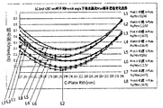
- Figure 5 shows the variation of the amount of light leakage with the delay value during the simulation of the liquid crystal display. line;
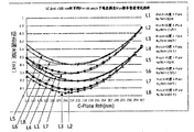
- Figure 6 shows the variation of the amount of light leakage with the delay value during the simulation of the liquid crystal display. line;
- Figure 7 is a diagram showing the use of the compensation values of an embodiment of the present invention for A-Plate and C-Plate Schematic diagram of brightness distribution such as dark state light leakage;
- Figure 8 is a diagram showing the use of the compensation values of an embodiment of the present invention by the A-Plate and the C-Plate Schematic diagram of the same contrast distribution for full viewing angle;
- Figure 9 is a diagram showing the compensation values of another embodiment of the present invention after the A-Plate and the C-Plate are used. Schematic diagram of brightness distribution such as dark state light leakage;
- Figure 10 is a diagram showing the compensation values of another embodiment of the present invention after the A-Plate and the C-Plate are used. A schematic view of the same contrast distribution of the full viewing angle;
- Figure 11 is a diagram showing the compensation values of another embodiment of the present invention after the A-Plate and the C-Plate are used. Schematic diagram of brightness distribution such as dark state light leakage;
- Figure 12 is a diagram showing the compensation values of another embodiment of the present invention after the A-Plate and the C-Plate are used. A schematic view of the same contrast distribution for a full view.
- FIG. 3 is a first preferred embodiment of a liquid crystal display according to an embodiment of the present invention. A schematic structural view of an embodiment.
- the liquid crystal display of the embodiment of the invention is preferably vertical alignment (Vertical Alignment, VA) liquid crystal display, liquid crystal optical path difference LC of the liquid crystal display ⁇ ND range 287nm ⁇ LC ⁇ ND ⁇ 305nm, ie interval [287nm, 305nm];
- the liquid crystal pretilt angle Pretilt angle ranges from 85° ⁇ Pretilt angle ⁇ 90°, ie Interval [85°, 90°).
- the liquid crystal display includes a first substrate 31.
- the second substrate 32, the liquid crystal layer 33, the first polarizing film 34, and the second polarizing film 35 also includes a positive hyperbolic uniaxial A-compensation film 36 and a negative hyperbolic uniaxial C-compensation film 37.
- the liquid crystal layer 33 is disposed on the first substrate 31 and the second base
- the first polarizing film 34 is disposed outside the first substrate 31 between the boards 32.
- the second polarizing film 35 is disposed outside the second substrate 32.
- the positive hyperbolic uniaxial A-compensation film 36 and a negative hyperbolic uniaxial C-compensation film 37 is disposed on the same side of the liquid crystal layer and is disposed On the first substrate 31 and the first polarizing film 34 or the second substrate 31 and Between the two polarizing films 35.
- the positive double zigzag single axis The A-compensation film 36 and the negative hyperbolic uniaxial C-compensation film 37 are attached and connected, and The first substrate 31 and the first polarizing film 34 are disposed.
- the compensation film has the same slow axis, which is perpendicular to the absorption axis of the first polarizing film.
- the positive double zigzag single axis The A-compensation film 36 and the negative hyperbolic uniaxial C-compensation film 37 are attached and connected, and The second substrate 32 and the second polarizing film 35 are disposed.
- the positive hyperbolic The uniaxial A-compensation film and the negative hyperbolic uniaxial C-compensation film have the same slowness a shaft that is perpendicular to an absorption axis of the second polarizing film.
- the first polarizing film 34 is sucked The axis of retraction is 0 degrees, and the absorption axis of the second polarizing film 35 is 90 degrees; in some other In an embodiment, the absorption axis of the first polarizing film 34 is 90 degrees, and the second bias When the absorption axis of the light film 35 is 0 degree, as long as the positive double zigzag single axis A-fill is ensured
- the slow axis of the compensation film 36 and the negative hyperbolic uniaxial C-compensation film 37 are respectively in the liquid a polarizing film (first polarizing film 34 or second polarizing film 35) on the same side of the crystal layer 33
- the absorption axis is vertical and is suitable for use in the present invention.
- the present invention provides a different positive hyperbolic uniaxial A-compensation film 36 by providing And a compensation value of the negative hyperbolic uniaxial C-compensation film 37 to simulate dark state light leakage, and According to the simulation result, the compensation value range corresponding to the dark state light leakage is obtained.
- the simulation process first set the positive Spherical double-axis A-compensation film 36 and negative hyperbolic uniaxial C-compensation film 37
- the angle between the slow axis and its corresponding polarizing film absorption axis is 90°, and the liquid crystal display
- the liquid crystal pretilt angle is set in the range [85°, 90°); the liquid in the four quadrants
- the crystal azimuth angle pretwist is set to 45°
- the liquid crystal optical path difference LC ⁇ ND is set in the region.
- the source used for the simulation is Blu-ray (Yttrium) Aluminum Garnet) LED spectrum with a central brightness defined as 100 nit, source
- the distribution is the Lambert distribution.
- Rth represents the thickness direction retardation Rth of the negative hyperbolic uniaxial C-compensation film 37
- A-Plate Ro represents the in-plane retardation Ro of the positive hyperbolic uniaxial A-compensation film 36
- A-Plate Rth represents the thickness direction retardation of the positive hyperbolic uniaxial A-compensation film 36 Rth.
- In-plane optical path compensation value Ro of the positive hyperbolic uniaxial A-compensation film 36 The value range is: 92nm ⁇ Ro ⁇ 184nm, and its out-of-plane optical path difference compensation value Rth The range of values is: 46nm ⁇ Rth ⁇ 92nm; the negative hyperbolic uniaxial C-compensation
- the compensation value Rth of the film 37 ranges from Y1 ⁇ Rth ⁇ Y2, where Y1 and Y2 Satisfy the following formulas (1) and (2):
- Nx is given in the plane of the positive hyperbolic uniaxial A-compensation film 36
- the refractive index in the X direction of the maximum refractive index, Ny is the positive hyperbolic uniaxial A-
- Nz is the positive
- d1 is the positive double
- Off-plane optical path difference compensation value Rth of the negative hyperbolic uniaxial C-compensation film 37 The range is adjusted by the following formula (5):
- Mx is the maximum fold given in the face of the negative hyperbolic uniaxial C-compensation film 37
- My is a negative hyperbolic uniaxial C-compensation film 37
- the refractive index in the Y direction orthogonal to the X direction, Mz is a negative hyperbolic uniaxial C-
- the refractive index of the compensation film 37 in the thickness direction, d2 is a negative hyperbolic uniaxial C-compensation film
- the thickness of 37, and Mx My, My > Mz.
- the range of the in-plane optical path difference compensation value Ro is adjusted to be: 92 nm ⁇ Ro ⁇ 184 nm
- the range of the out-of-plane optical path difference compensation value Rth is adjusted to be: 46 nm ⁇ Rth ⁇ 92nm.
- the compensation value Rth of the negative hyperbolic uniaxial C-compensation film 37 is The range of values is adjusted to Y1 ⁇ Rth ⁇ Y2.
- the range of the in-plane optical path difference compensation value Ro of 36 is adjusted to be: 92 nm ⁇ Ro ⁇
- the range of the out-of-plane optical path difference compensation value Rth is adjusted to: 46 nm ⁇ Rth ⁇ 92 nm.
- the compensation value Rth of the negative hyperbolic uniaxial C-compensation film 37 is The range of values is adjusted to Y1 ⁇ Rth ⁇ Y2.
- the circumference adjustment is: 92nm ⁇ Ro ⁇ 184nm, and the out-of-plane optical path difference compensation value Rth is taken.
- the value range is adjusted to: 46 nm ⁇ Rth ⁇ 92 nm; then, the negative double is simultaneously adjusted
- the refractive index Mx, My, Mz and thickness d2 of the meandering uniaxial C-compensation film 37 are Formula (5), the compensation value Rth of the negative hyperbolic uniaxial C-compensation film 37
- the value range is adjusted to Y1 ⁇ Rth ⁇ Y2.
- the brightness distribution effect of the dark state light leakage and the like using the compensation value of the embodiment of the present invention is shown
- the intents 7, 9, and 11 are compared with the prior art effect diagram 1 to obtain:
- the maximum value of the dark state leakage after compensation by the uniaxial C-compensation film 37 is 2.5 nit (ni Special) reduced to below 0.2nit.
- the same contrast distribution effect of the full viewing angle of the compensation value of the embodiment of the present invention will be used.
- the schematic diagrams 8, 10, and 12 are compared with the prior art effect diagram 2, and Out: Positive hyperbolic uniaxial A-compensation film 36 using the compensation value of the embodiment of the present invention
- the full-view contrast distribution after compensation with the negative hyperbolic uniaxial C-compensation film 37 is better than The full-view contrast distribution of the prior art.
- the present invention improves the prior art The problem of serious dark light leakage caused by A-plate and C-plate compensation values, Effectively improves the contrast and viewing clarity of large viewing angles (non-horizontal vertical azimuth) Clearness.
- the invention also provides an optical compensation method using a liquid crystal display, the method needle For a VA liquid crystal display, the liquid crystal optical path difference LC ⁇ ND of the liquid crystal display
- the range is [287 nm, 305 nm]
- the liquid crystal pretilt angle range is [85°, 90°).
- the liquid crystal display comprises a positive hyperbolic uniaxial A-compensation film 36 and a Negative hyperbolic uniaxial C-compensation film 37, said positive hyperbolic uniaxial A-compensation film 36 And a negative hyperbolic uniaxial C-compensation film 37 is disposed on the same side of the liquid crystal layer 33, And disposed on the first substrate 31 and the first polarizing film 34 or the second substrate Between 33 and the second polarizing film 35, for example, please refer to FIG. 3 and FIG.
- Y2 -0.00005073x 4 +0.013658x 3 -1.3931x 2 +63.85x-853.5;
- X is the out-of-plane optical path difference compensation value Rth of the positive hyperbolic uniaxial A-compensation film 36.
- the positive hyperbolic uniaxial A-compensation film 36 is adjusted.
- the in-plane optical path difference compensation value Ro has a value range of 92 nm ⁇ Ro ⁇ 184 nm, and is adjusted.
- the out-of-plane optical path difference compensation value Rth of the positive double-folded uniaxial A-compensation film 36 When the value ranges from 46 nm ⁇ Rth ⁇ 92 nm, it is adjusted by the following formula:
- Nx is given in the plane of the positive hyperbolic uniaxial A-compensation film 36
- the refractive index in the X direction of the maximum refractive index, Ny is the positive hyperbolic uniaxial A-
- Nz is the positive
- d1 is the positive double
- Mx is the maximum fold given in the face of the negative hyperbolic uniaxial C-compensation film 37
- the refractive index in the X direction of the incident rate, My is a negative hyperbolic uniaxial C-compensation film surface 37
- the refractive index in the Y direction orthogonal to the X direction, Mz is a negative hyperbolic uniaxial C-
- the refractive index of the compensation film 37 in the thickness direction, d2 is a negative hyperbolic uniaxial C-compensation film
- the thickness of 37, and Mx My, My > Mz.
- the embodiment of the invention is mainly for the liquid crystal optical path difference LC ⁇ ND at [287 nm, 305nm], two optical compensation films with a liquid crystal pretilt angle range of [85°, 90°): Positive double-folded single-axis A-compensation film and negative double-folded single-axis C-compensation film Compensating the compensation values of the above two compensation films to weaken the dark state light leakage phenomenon at a large viewing angle, and implementing The invention can effectively increase the large viewing angle (non-horizontal, vertical azimuth angle) Contrast and clarity.
Landscapes
- Physics & Mathematics (AREA)
- Nonlinear Science (AREA)
- Mathematical Physics (AREA)
- Chemical & Material Sciences (AREA)
- Crystallography & Structural Chemistry (AREA)
- General Physics & Mathematics (AREA)
- Optics & Photonics (AREA)
- Polarising Elements (AREA)
- Liquid Crystal (AREA)
Abstract
一种液晶显示器及其光学补偿方法,主要是改变正性双曲折单轴A-补偿膜和负性双曲折单轴C-补偿膜的补偿值,尤其是控制负性双曲折单轴C-补偿膜的补偿值Rth的取值范围,通过调整上述两种补偿膜的补偿值来减弱暗态漏光现象,实施本技术方案可以有效的减弱大视角的暗态漏光现象,增加大视角的对比度和清晰度。
Description
本发明涉及液晶显示技术领域,特别是涉及一种液晶显示器
及其光学补偿方法。
随着液晶显示面板的不断普及,对液晶显示面板显示质量的
要求越来越高。为了获得较高的液晶光程差,在液晶折射率固定
的情况下,只能增加液晶的厚度(cell gap),这样会导致液晶用
量的增加,由于液晶的成本很高,因此液晶用量越多,生产成本
就越高。
而液晶光程差的大小不仅关系到穿透率的高低,也会对大视
角的暗态漏光造成很大的影响。以薄膜场效应晶体管液晶显示器
(Thin Film Transistor LCD,TFT-LCD)为例,随着TFT-LCD
的观察角度逐渐增大,画面的对比度不断降低,画面的清晰度也
逐渐下降。这是由于液晶层中液晶分子的双折射率随着观察角度
变化发生改变的结果,采用宽视角补偿膜进行补偿,可以有效降
低暗态画面的漏光,在一定的视角内能大幅度提高画面的对比
度。
其中补偿膜的补偿原理一般是将液晶在不同视角产生的相
位差进行修正,让液晶分子的双折射性质得到对称性的补偿。
针对不同的液晶显示模式,使用的补偿膜也不同,大尺寸液
晶电视使用的补偿膜大多是针对垂直配向(Vertical Alignment,
VA)显示模式,早期使用的有Konica公司的N-TAC,后来不断
发展形成OPOTES公司的Zeonor,富士通的F-TAC系列,日东
电工的X-Plate等。
而针对相同的液晶光程差,如果补偿膜补偿值不同,则大视
角的暗态漏光就不同,对比度也不同。请参阅图1和图2,图1
为现有技术中使用正性双曲折单轴A-补偿膜(unaxial positive
birefringence A-Plate)与负性双曲折单轴C-补偿膜(unaxial
Negative birefringence C-Plate)补偿暗态漏光等亮度分布
(Isoluminance contour)示意图,图2为现有技术中使用A-Plate
与C-Plate补偿后的全视角相同对比度分布(Equal contrast ratio
contour)示意图,其中上述A-Plate与C-Plate补偿值如下表:
| 液晶光程差 | A-PlateRo | A-PlateRth | C-PlateRth |
| 305nm | 109.2nm | 54.6nm | 402.6nm |
从图1和图2不难看出,采用现有技术的A-Plate与C-Plate
补偿值,在暗态下观看大视角会有严重漏光现象,大视角的对比
度会变得较差,视角范围很小。
因此,需解决上述技术问题。
【发明内容】
本发明的目的在于提供一种液晶显示器及其光学补偿方法,
旨在现有技术中A-Plate与C-Plate的补偿值在暗态下观看大视
角会有严重漏光现象,大视角的对比度会变得较差,视角范围很
小的技术问题。
为解决上述技术问题,本发明构造了一种液晶显示器,其中
所述液晶显示器的液晶光程差LC△ND范围为287nm≤LC△ND
≤305nm,所述液晶显示器包括:
第一基板;
第二基板;
液晶层,设置于所述第一基板和所述第二基板之间;
第一偏光膜,设置于所述第一基板的外侧;
第二偏光膜,设置于所述第二基板的外侧;
一正性双曲折单轴A-补偿膜;以及
一负性双曲折单轴C-补偿膜,所述正性双曲折单轴A-补偿
膜及所述负性双曲折单轴C-补偿膜设置于所述第一基板与所述
第一偏光膜之间或者所述第二基板与所述第二偏光膜之间;
其中,所述正性双曲折单轴A-补偿膜的面内光程差补偿值
Ro的取值范围为92nm≤Ro≤184nm,其面外光程差补偿值Rth
的取值范围为46nm≤Rth≤92nm;所述负性双曲折单轴C-补偿
膜的补偿值Rth的取值范围为Y1≤Rth≤Y2;其中Y1、Y2满足
下式:
Y1=-0.00003316x3+0.08074x2–10.84x+520.2;以及
Y2=-0.00005073x4+0.013658x3-1.3931x2+63.85x-853.5;
X为所述正性双曲折单轴A-补偿膜的面外光程差补偿值
Rth。
在本发明的液晶显示器中,其中所述正性双曲折单轴A-补
偿膜的面内光程差补偿值Ro以及面外光程差补偿值Rth的范围
通过如下公式调整获得:
Ro=(Nx-Ny)*d1;以及
Rth=[(Nx+Ny)/2-Nz]*d1
其中,Nx为所述正性双曲折单轴A-补偿膜面内给出的最大
折射率的X方向的折射率,Ny为所述正性双曲折单轴A-补偿膜
面内与X方向正交的Y方向的折射率,Nz为所述正性双曲折单
轴A-补偿膜厚度方向的折射率,d1为所述正性双曲折单轴A-补
偿膜的厚度,且Nx﹥Ny,且Ny=Nz。
在本发明的液晶显示器中,其中所述负性双曲折单轴C-补
偿膜的补偿值Rth的范围通过如下公式调整获得:
Rth=[(Mx+My)/2-Mz]*d2;
其中Mx为所述负性双曲折单轴C-补偿膜面内给出的最大
折射率的X方向的折射率,My为所述负性双曲折单轴C-补偿膜
面内与X方向正交的Y方向的折射率,Mz为所述负性双曲折单
轴C-补偿膜厚度方向的折射率,d2为所述负性双曲折单轴C-补
偿膜的厚度,Mx=My,且My﹥Mz。
在本发明的液晶显示器中,其中所述一正性双曲折单轴A-
补偿膜以及一负性双曲折单轴C-补偿膜设置于所述液晶层的同
侧,且设置于所述第一基板与所述第一偏光膜之间。
在本发明的液晶显示器中,其中所述一正性双曲折单轴A-
补偿膜以及一负性双曲折单轴C-补偿膜设置于所述液晶层的同
侧,且设置于所述第二基板与所述第二偏光膜之间。
本发明构造了一种液晶显示器,所述液晶显示器包括:第一
基板;
第二基板;
液晶层,设置于所述第一基板和所述第二基板之间;
第一偏光膜,设置于所述第一基板的外侧;
第二偏光膜,设置于所述第二基板的外侧;
一正性双曲折单轴A-补偿膜;以及
一负性双曲折单轴C-补偿膜,所述正性双曲折单轴A-补偿
膜及所述负性双曲折单轴C-补偿膜设置于所述第一基板与所述
第一偏光膜之间或者所述第二基板与所述第二偏光膜之间;
其中,所述正性双曲折单轴A-补偿膜的面内光程差补偿值
Ro的取值范围为92nm≤Ro≤184nm,其面外光程差补偿值Rth
的取值范围为46nm≤Rth≤92nm;所述负性双曲折单轴C-补偿
膜的补偿值Rth的取值范围为Y1≤Rth≤Y2;其中Y1、Y2满足
下式:
Y1=-0.00003316x3+0.08074x2–10.84x+520.2;
Y2=-0.00005073x4+0.013658x3-1.3931x2+63.85x-853.5;
X为所述正性双曲折单轴A-补偿膜的面外光程差补偿值
Rth。
在本发明的液晶显示器中,所述正性双曲折单轴A-补偿膜
的面内光程差补偿值Ro以及面外光程差补偿值Rth的范围通过
如下公式调整获得:
Ro=(Nx-Ny)*d1;
Rth=[(Nx+Ny)/2-Nz]*d1
其中,Nx为所述正性双曲折单轴A-补偿膜面内给出的最大
折射率的X方向的折射率,Ny为所述正性双曲折单轴A-补偿膜
面内与X方向正交的Y方向的折射率,Nz为所述正性双曲折单
轴A-补偿膜厚度方向的折射率,d1为所述正性双曲折单轴A-补
偿膜的厚度,且Nx﹥Ny,且Ny=Nz。
在本发明的液晶显示器中,所述负性双曲折单轴C-补偿膜
的补偿值Rth的范围通过如下公式调整获得:
Rth=[(Mx+My)/2-Mz]*d2;
其中Mx为所述负性双曲折单轴C-补偿膜面内给出的最大
折射率的X方向的折射率,My为所述负性双曲折单轴C-补偿膜
面内与X方向正交的Y方向的折射率,Mz为所述负性双曲折单
轴C-补偿膜厚度方向的折射率,d2为所述负性双曲折单轴C-补
偿膜的厚度,Mx=My,且My﹥Mz。
在本发明的液晶显示器中,所述一正性双曲折单轴A-补偿
膜以及一负性双曲折单轴C-补偿膜设置于所述液晶层的同侧,
且设置于所述第一基板与所述第一偏光膜之间或者所述第二基
板与所述第二偏光膜之间。
为解决上述技术问题,本发明还构造了一种液晶显示器的光
学补偿方法,所述方法包括:
调整所述正性双曲折单轴A-补偿膜的面内光程差补偿值Ro
的取值范围在92nm≤Ro≤184nm;
调整所述正性双曲折单轴A-补偿膜的面外光程差补偿值
Rth的取值范围在46nm≤Rth≤92nm;以及
调整所述负性双曲折单轴C-补偿膜的补偿值Rth的取值范
围在Y1≤Rth≤Y2;其中Y1、Y2满足下式:
Y1=-0.00003316x3+0.08074x2–10.84x+520.2;
Y2=-0.00005073x4+0.013658x3-1.3931x2+63.85x-853.5;
X为所述正性双曲折单轴A-补偿膜的面外光程差补偿值
Rth;所述正性双曲折单轴A-补偿膜以及负性双曲折单轴C-补偿
膜设置于所述液晶显示器的第一基板与第一偏光膜之间或者第
二基板与第二偏光膜之间。
在本发明的液晶显示器的光学补偿方法中,其中调整所述正
性双曲折单轴A-补偿膜的面内光程差补偿值Ro的取值范围在
92nm≤Ro≤184nm,并调整所述正性双曲折单轴A-补偿膜的面
外光程差补偿值Rth的取值范围在46nm≤Rth≤92nm时,通过
下式进行调整获得:
Ro=(Nx-Ny)*d1;
Rth=[(Nx+Ny)/2-Nz]*d1
其中,Nx为所述正性双曲折单轴A-补偿膜面内给出的最大
折射率的X方向的折射率,Ny为所述正性双曲折单轴A-补偿膜
面内与X方向正交的Y方向的折射率,Nz为所述正性双曲折单
轴A-补偿膜厚度方向的折射率,d1为所述正性双曲折单轴A-补
偿膜的厚度,Nx﹥Ny,且Ny=Nz。
在本发明的液晶显示器的光学补偿方法中,其中调整所述负
性双曲折单轴C-补偿膜的补偿值Rth的取值范围在Y1≤Rth≤
Y2时,通过下式调整获得:
Rth=[(Mx+My)/2-Mz]*d2;
其中Mx为所述负性双曲折单轴C-补偿膜面内给出的最大
折射率的X方向的折射率,My为所述负性双曲折单轴C-补偿膜
面内与X方向正交的Y方向的折射率,Mz为所述负性双曲折单
轴C-补偿膜厚度方向的折射率,d2为所述负性双曲折单轴C-补
偿膜的厚度,Mx=My,且My﹥Mz。
在本发明的液晶显示器的光学补偿方法中,所述一正性双曲
折单轴A-补偿膜以及所述一负性双曲折单轴C-补偿膜设置于所
述液晶层的同侧,且设置于所述第一基板与所述第一偏光膜之间
或者所述第二基板与所述第二偏光膜之间。
本发明通过改变液晶显示器中正性双曲折单轴A-补偿膜和
负性双曲折单轴C-补偿膜的补偿值来减弱大视角的暗态漏光现
象,实施本发明可以有效的增加大视角(非水平,垂直方位角的
大视角)的对比度和清晰度。
为让本发明的上述内容能更明显易懂,下文特举优选实施
例,并配合所附图式,作详细说明如下:
图1为现有技术中使用A-Plate和C-Plate的补偿值补偿暗
态漏光等亮度分布示意图;
图2为现有技术中使用A-Plate和C-Plate的补偿值补偿后
全视角相同对比度分布示意图;
图3为本发明液晶显示器的第一较佳实施例结构示意图;
图4为本发明液晶显示器的第二较佳实施例结构示意图;
图5为液晶显示器在模拟过程中漏光量随延迟值的变化曲
线;
图6为液晶显示器在模拟过程中漏光量随延迟值的变化曲
线;
图7为A-Plate和C-Plate使用本发明一实施例补偿值后的
暗态漏光等亮度分布示意图;
图8为A-Plate和C-Plate使用本发明一实施例补偿值后的
全视角相同对比度分布示意图;
图9为A-Plate和C-Plate使用本发明另一实施例补偿值后
的暗态漏光等亮度分布示意图;
图10为A-Plate和C-Plate使用本发明另一实施例补偿值后
的全视角相同对比度分布示意图;
图11为A-Plate和C-Plate使用本发明又一实施例补偿值后
的暗态漏光等亮度分布示意图;
图12为A-Plate和C-Plate使用本发明又一实施例补偿值后
的全视角相同对比度分布示意图。
以下各实施例的说明是参考附加的图式,用以例示本发明可
用以实施的特定实施例。本发明所提到的方向用语,例如「上」、
「下」、「前」、「后」、「左」、「右」、「内」、「外」、「侧面」等,仅
是参考附加图式的方向。因此,使用的方向用语是用以说明及理
解本发明,而非用以限制本发明。在图中,结构相似的单元是以
相同标号表示。
请参阅图3,图3为本发明实施例中液晶显示器的第一较佳
实施例结构示意图。
本发明实施例的所述液晶显示器优选为垂直配向(Vertical
Alignment,VA)液晶显示器,所述液晶显示器的液晶光程差LC
△ND范围287nm≤LC△ND≤305nm,即区间[287nm,305nm];
而液晶预倾角Pretilt angle的范围85°≤Pretilt angle<90°,即
区间[85°,90°)。
在图3所示的第一实施例中,所述液晶显示器包括第一基板
31、第二基板32、液晶层33、第一偏光膜34和第二偏光膜35,
还包括一正性双曲折单轴A-补偿膜36以及一负性双曲折单轴
C-补偿膜37。所述液晶层33设置于所述第一基板31和第二基
板32之间,所述第一偏光膜34设置于所述第一基板31的外侧,
所述第二偏光膜35设置于所述第二基板32的外侧。
在具体实施过程中,所述正性双曲折单轴A-补偿膜36以及
负性双曲折单轴C-补偿膜37设置于所述液晶层的同侧,并设置
于所述第一基板31与所述第一偏光膜34或者第二基板31与第
二偏光膜35之间。
譬如在图3所示的第一较佳实施例中,所述正性双曲折单轴
A-补偿膜36以及负性双曲折单轴C-补偿膜37贴合连接,且设
置于所述第一基板31与所述第一偏光膜34之间。
所述正性双曲折单轴A-补偿膜和所述负性双曲折单轴C-补
偿膜具有相同的慢轴,该慢轴与所述第一偏光膜的吸收轴垂直。
而在图4所示的第二较佳实施例中,所述正性双曲折单轴
A-补偿膜36以及负性双曲折单轴C-补偿膜37贴合连接,且设
置于所述第二基板32与所述第二偏光膜35之间。所述正性双曲
折单轴A-补偿膜和所述负性双曲折单轴C-补偿膜具有相同的慢
轴,该慢轴与所述第二偏光膜的吸收轴垂直。
上述液晶显示器的较佳实施例中,所述第一偏光膜34的吸
收轴为0度,所述第二偏光膜35的吸收轴为90度;在一些其它
实施例中,所述第一偏光膜34的吸收轴为90度、且所述第二偏
光膜35的吸收轴为0度时,只要保证所述正性双曲折单轴A-补
偿膜36以及负性双曲折单轴C-补偿膜37的慢轴分别与其在液
晶层33同一侧的偏光膜(第一偏光膜34或第二偏光膜35)的
吸收轴垂直即可,均适用于本发明。
其中,本发明通过设置不同的正性双曲折单轴A-补偿膜36
以及负性双曲折单轴C-补偿膜37的补偿值来模拟暗态漏光,并
根据模拟结果获取暗态漏光对应的补偿值范围。
为了获得最佳的补偿效果,在模拟过程中,首先设置所述正
性双曲折单轴A-补偿膜36以及负性双曲折单轴C-补偿膜37的
慢轴与其对应的偏光膜吸收轴的夹角为90°,并将所述液晶显示
器的液晶预倾角设置在范围为[85°,90°);将四个象限内的液
晶方位角pretwist设置为45°,将液晶光程差LC△ND设置在区
间[287nm,305nm];并且模拟使用的光源为蓝光-YAG(Yttrium
Aluminum Garnet)LED光谱,其中央亮度定义为100nit,光源
分布为朗伯(Lambert)分布。
模拟结果请参阅图5和6所示的漏光量随延迟值的变化曲线
示意图,其中图5所示为在液晶光程差LC△ND为287nm,预倾
角为89°和85°时,所述正性双曲折单轴A-补偿膜36的面内延
迟Ro和厚度方向延迟Rth、以及负性双曲折单轴C-补偿膜37
的厚度方向延迟Rth取不同值时的漏光量变化曲线示意图;图6
所示液晶光程差为LC△ND为305nm、预倾角为89°和85°时,
所述正性双曲折单轴A-补偿膜36的面内延迟Ro和厚度方向延
迟Rth、以及负性双曲折单轴C-补偿膜37的厚度方向延迟Rth
取不同值时的漏光量变化曲线示意图。在图5和图6中的C-Plate
Rth表示负性双曲折单轴C-补偿膜37的厚度方向延迟Rth,
A-Plate Ro表示正性双曲折单轴A-补偿膜36的面内延迟Ro,
A-Plate Rth表示正性双曲折单轴A-补偿膜36的厚度方向延迟
Rth。
通过上述模拟,得出在不同预倾角下,所述正性双曲折单轴
A-补偿膜36与所述负性双曲折单轴C-补偿膜37的补偿值对暗
态漏光的影响趋势是一致的,即在不同预倾角下,暗态漏光最小
时对应的补偿值范围是一样的,并根据模拟结果得出液晶光程差
LC△ND在[287nm,305nm]、预倾角在[85°,90°)、暗态漏光
小于0.2nit(预倾角=89°时模拟出的暗态漏光值,非实测值)时
对应的正性双曲折单轴A-补偿膜36和负性双曲折单轴C-补偿膜
37的延迟值范围如下:
所述正性双曲折单轴A-补偿膜36的面内光程差补偿值Ro
的取值范围为:92nm≤Ro≤184nm,其面外光程差补偿值Rth
的取值范围为:46nm≤Rth≤92nm;所述负性双曲折单轴C-补偿
膜37的补偿值Rth的取值范围为Y1≤Rth≤Y2,其中Y1、Y2
满足下式(1)和(2):
Y1=-0.00003316x3+0.08074x2–10.84x+520.2 (1)
Y2=-0.00005073x4+0.013658x3-1.3931x2+63.85x-853.5 (2)
其中上式(1)和(2)中的X为所述正性双曲折单轴A-补
偿膜的面外光程差补偿值Rth。
上述补偿值范围用表格表示如下:

具体的,所述正性双曲折单轴A-补偿膜36的面内光程差补
偿值Ro以及面外光程差补偿值Rth的范围通过如下公式(3)和
(4)调整获得:
Ro=(Nx-Ny)*d1; (3)
Rth=[(Nx+Ny)/2-Nz]*d1; (4)
其中,Nx为所述正性双曲折单轴A-补偿膜36面内给出的
最大折射率的X方向的折射率,Ny为所述正性双曲折单轴A-
补偿膜36面内与X方向正交的Y方向的折射率,Nz为所述正
性双曲折单轴A-补偿膜36厚度方向的折射率,d1为所述正性双
曲折单轴A-补偿膜36的厚度,且Nx﹥Ny,Ny=Nz。
所述负性双曲折单轴C-补偿膜37的面外光程差补偿值Rth
的范围通过如下公式(5)调整获得:
Rth=[(Mx+My)/2-Mz]*d2; (5)
其中Mx为负性双曲折单轴C-补偿膜37面内给出的最大折
射率的X方向的折射率,My为负性双曲折单轴C-补偿膜37面
内与X方向正交的Y方向的折射率,Mz为负性双曲折单轴C-
补偿膜37厚度方向的折射率,d2为负性双曲折单轴C-补偿膜
37的厚度,且Mx=My,My﹥Mz。
譬如,以下面三个实施例A、B、C来进一步阐述如何根据
上述公式(3)、(4)以及(5)来对正性双曲折单轴A-补偿膜36
和负性双曲折单轴C-补偿膜37进行调整。
(A):当已知所述正性双曲折单轴A-补偿膜36的折射率Nx、
Ny、Nz的值时,调整所述正性双曲折单轴A-补偿膜36的厚度
d1,根据公式(3)和(4),将所述正性双曲折单轴A-补偿膜36
的面内光程差补偿值Ro的取值范围调整为:92nm≤Ro≤184nm,
将其面外光程差补偿值Rth的取值范围调整为:46nm≤Rth≤
92nm。
当已知所述负性双曲折单轴C-补偿膜37的折射率Mx、My、
Mz的值时,调整所述负性双曲折单轴C-补偿膜37的厚度d2,
根据公式(5),将所述负性双曲折单轴C-补偿膜37的补偿值Rth
的取值范围调整为Y1≤Rth≤Y2。
(B):当已知所述正性双曲折单轴A-补偿膜36的厚度d1的
值时,根据公式(3)和(4)调整所述正性双曲折单轴A-补偿
膜36的折射率Nx、Ny、Nz,将所述正性双曲折单轴A-补偿膜
36的面内光程差补偿值Ro的取值范围调整为:92nm≤Ro≤
184nm,将其面外光程差补偿值Rth的取值范围调整为:46nm≤
Rth≤92nm。
当已知所述负性双曲折单轴C-补偿膜37的厚度d2的值时,
调整所述负性双曲折单轴C-补偿膜37的折射率Mx、My、Mz,
根据公式(5),将所述负性双曲折单轴C-补偿膜37的补偿值Rth
的取值范围调整为Y1≤Rth≤Y2。
(C):首先,同时调整所述正性双曲折单轴A-补偿膜37的
折射率Nx、Ny、Nz和厚度d1,根据公式(3)和(4),将所述
正性双曲折单轴A-补偿膜36的面内光程差补偿值Ro的取值范
围调整为:92nm≤Ro≤184nm,将其面外光程差补偿值Rth的取
值范围调整为:46nm≤Rth≤92nm;然后,同时调整所述负性双
曲折单轴C-补偿膜37的折射率Mx、My、Mz和厚度d2,根据
公式(5),将所述负性双曲折单轴C-补偿膜37的补偿值Rth的
取值范围调整为Y1≤Rth≤Y2。
以下以三个具体的实施例1)、2)和3)来说明本发明的技
术效果:
1)、选取液晶光程差LC△ND=296nm,预倾角=89°,所述
正性双曲折单轴A-补偿膜36的补偿值Ro=144nm,Rth=72nm,
所述负性双曲折单轴C-补偿膜37的补偿值Rth=167nm,上述补
偿值对应的暗态漏光等亮度分布图如图7所示,对应的全视角相
同对比度分布图如图8所示,其中上述补偿值的表格如下:

2)、选取液晶光程差LC△ND=296nm,预倾角=89°,所述
正性双曲折单轴A-补偿膜36的补偿值Ro=144nm,Rth=72nm,
所述负性双曲折单轴C-补偿膜37的补偿值Rth=199nm,上述补
偿值对应的暗态漏光等亮度分布图如图9所示,对应的全视角相
同对比度分布图如图10所示,其中上述补偿值的表格如下:

3)、选取液晶光程差LC△ND=296nm,预倾角=89°,所述
正性双曲折单轴A-补偿膜36的补偿值Ro=144nm,Rth=72nm,
所述负性双曲折单轴C-补偿膜37的补偿值Rth=238nm,上述补
偿值对应的暗态漏光等亮度分布图如图11所示,对应的全视角
相同对比度分布图如图12所示,其中上述补偿值的表格如下:

将使用本发明实施例补偿值的暗态漏光等亮度分布效果示
意图7、9、11与现有技术的效果示意图1进行对比,可以得出:
使用本发明实施例的补偿值的正性双曲折单轴A-补偿膜36与负
性双曲折单轴C-补偿膜37补偿后的暗态漏光最大值由2.5nit(尼
特)降低到0.2nit以下。
将使用本发明实施例补偿值的全视角相同对比度分布效果
示意图8、10、12与现有技术的效果示意图2进行对比,可以得
出:使用本发明实施例的补偿值的正性双曲折单轴A-补偿膜36
与负性双曲折单轴C-补偿膜37补偿后的全视角对比度分布优于
现有技术的全视角对比度分布。由此,本发明改善了现有技术中
使用A-plate与C-plate补偿值造成的暗态漏光严重现象的问题,
有效地提高了大视角(非水平垂直方位角)的对比度和观看的清
晰度。
本发明还提供一种使用液晶显示器光学补偿方法,该方法针
对VA液晶显示器而言,所述液晶显示器的液晶光程差LC△ND
范围为[287nm,305nm],其液晶预倾角范围为[85°,90°)。
其中所述液晶显示器包括一正性双曲折单轴A-补偿膜36以及一
负性双曲折单轴C-补偿膜37,所述正性双曲折单轴A-补偿膜36
以及负性双曲折单轴C-补偿膜37设置于所述液晶层33的同侧,
且设置于所述第一基板31与所述第一偏光膜34或者第二基板
33与第二偏光膜35之间,譬如请参阅图3和图4。
而本发明实施例的液晶显示器光学补偿方法包括:
(Ⅰ)、将正性双曲折单轴A-补偿膜36的面内光程差补偿
值Ro的取值范围调整为92nm≤Ro≤184nm。
(Ⅱ)、将正性双曲折单轴A-补偿膜36面外光程差补偿值
Rth的取值范围调整为46nm≤Rth≤92nm。
(Ⅲ)、将负性双曲折单轴C-补偿膜37的补偿值Rth的取
值范围调整为Y1≤Rth≤Y2;其中:
Y1=-0.00003316x3+0.08074x2–10.84x+520.2;
Y2=-0.00005073x4+0.013658x3-1.3931x2+63.85x-853.5;
X为正性双曲折单轴A-补偿膜36的面外光程差补偿值Rth。
需要说明的是,上述步骤(Ⅰ)、(Ⅱ)和(Ⅲ)并不分先后。
在具体实施过程中,调整所述正性双曲折单轴A-补偿膜36
的面内光程差补偿值Ro的取值范围在92nm≤Ro≤184nm,并调
整所述正性双曲折单轴A-补偿膜36的面外光程差补偿值Rth的
取值范围在46nm≤Rth≤92nm时,通过下式进行调整获得:
Ro=(Nx-Ny)*d1;
Rth=[(Nx+Ny)/2-Nz]*d1;
其中,Nx为所述正性双曲折单轴A-补偿膜36面内给出的
最大折射率的X方向的折射率,Ny为所述正性双曲折单轴A-
补偿膜36面内与X方向正交的Y方向的折射率,Nz为所述正
性双曲折单轴A-补偿膜36厚度方向的折射率,d1为所述正性双
曲折单轴A-补偿膜36的厚度,且Nx﹥Ny,Ny=Nz。
在具体实施过程中,调整所述负性双曲折单轴C-补偿膜37
的补偿值Rth的取值范围在Y1≤Rth≤Y2时,通过下式调整获
得:
Rth=[(Mx+My)/2-Mz]*d2;
其中Mx为负性双曲折单轴C-补偿膜37面内给出的最大折
射率的X方向的折射率,My为负性双曲折单轴C-补偿膜面37
内与X方向正交的Y方向的折射率,Mz为负性双曲折单轴C-
补偿膜37厚度方向的折射率,d2为负性双曲折单轴C-补偿膜
37的厚度,且Mx=My,My﹥Mz。
具体的调整补偿值的过程请参阅上文针对液晶显示器的详
细描述,此处不再赘述。
本发明实施例主要是针对液晶光程差LC△ND在[287nm,
305nm],液晶预倾角范围为[85°,90°)的两种光学补偿膜:
正性双曲折单轴A-补偿膜和负性双曲折单轴C-补偿膜,通过调
整上述两种补偿膜的补偿值来减弱大视角的暗态漏光现象,实施
本发明可以有效的增加大视角(非水平,垂直方位角的大视角)
的对比度和清晰度。
综上所述,虽然本发明已以优选实施例揭露如上,但上述优
选实施例并非用以限制本发明,本领域的普通技术人员,在不脱
离本发明的精神和范围内,均可作各种更动与润饰,因此本发明
的保护范围以权利要求界定的范围为准。
Claims (15)
- 一种液晶显示器,其中所述液晶显示器的液晶光程差LC △ND范围为287nm≤LC△ND≤305nm,所述液晶显示器包括:第一基板;第二基板;液晶层,设置于所述第一基板和所述第二基板之间;第一偏光膜,设置于所述第一基板的外侧;第二偏光膜,设置于所述第二基板的外侧;一正性双曲折单轴A-补偿膜;以及一负性双曲折单轴C-补偿膜,所述正性双曲折单轴A-补偿 膜及所述负性双曲折单轴C-补偿膜设置于所述第一基板与所述 第一偏光膜之间或者所述第二基板与所述第二偏光膜之间;其中,所述正性双曲折单轴A-补偿膜的面内光程差补偿值 Ro的取值范围为92nm≤Ro≤184nm,其面外光程差补偿值Rth 的取值范围为46nm≤Rth≤92nm;所述负性双曲折单轴C-补偿 膜的补偿值Rth的取值范围为Y1≤Rth≤Y2;其中Y1、Y2满足 下式:Y1=-0.00003316x3+0.08074x2–10.84x+520.2;Y2=-0.00005073x4+0.013658x3-1.3931x2+63.85x-853.5;X为所述正性双曲折单轴A-补偿膜的面外光程差补偿值 Rth。
- 根据权利要求1所述的液晶显示器,其中所述正性双曲 折单轴A-补偿膜的面内光程差补偿值Ro以及面外光程差补偿值 Rth的范围通过如下公式调整获得:Ro=(Nx-Ny)*d1;以及Rth=[(Nx+Ny)/2-Nz]*d1其中,Nx为所述正性双曲折单轴A-补偿膜面内给出的最大 折射率的X方向的折射率,Ny为所述正性双曲折单轴A-补偿膜 面内与X方向正交的Y方向的折射率,Nz为所述正性双曲折单 轴A-补偿膜厚度方向的折射率,d1为所述正性双曲折单轴A-补 偿膜的厚度,且Nx﹥Ny,且Ny=Nz。
- 根据权利要求1所述的液晶显示器,其中所述负性双曲 折单轴C-补偿膜的补偿值Rth的范围通过如下公式调整获得:Rth=[(Mx+My)/2-Mz]*d2;其中Mx为所述负性双曲折单轴C-补偿膜面内给出的最大 折射率的X方向的折射率,My为所述负性双曲折单轴C-补偿膜 面内与X方向正交的Y方向的折射率,Mz为所述负性双曲折单 轴C-补偿膜厚度方向的折射率,d2为所述负性双曲折单轴C-补 偿膜的厚度,Mx=My,且My﹥Mz。
- 根据权利要求1所述的液晶显示器,其中所述一正性双 曲折单轴A-补偿膜以及一负性双曲折单轴C-补偿膜设置于所述 液晶层的同侧,且设置于所述第一基板与所述第一偏光膜之间。
- 根据权利要求1所述的液晶显示器,其中所述一正性双 曲折单轴A-补偿膜以及一负性双曲折单轴C-补偿膜设置于所述 液晶层的同侧,且设置于所述第二基板与所述第二偏光膜之间。
- 一种液晶显示器,其中所述液晶显示器包括:第一基板;第二基板;液晶层,设置于所述第一基板和所述第二基板之间;第一偏光膜,设置于所述第一基板的外侧;第二偏光膜,设置于所述第二基板的外侧;一正性双曲折单轴A-补偿膜;以及一负性双曲折单轴C-补偿膜,所述正性双曲折单轴A-补偿 膜及所述负性双曲折单轴C-补偿膜设置于所述第一基板与所述 第一偏光膜之间或者所述第二基板与所述第二偏光膜之间;其中,所述正性双曲折单轴A-补偿膜的面内光程差补偿值 Ro的取值范围为92nm≤Ro≤184nm,其面外光程差补偿值Rth 的取值范围为46nm≤Rth≤92nm;所述负性双曲折单轴C-补偿 膜的补偿值Rth的取值范围为Y1≤Rth≤Y2;其中Y1、Y2满足 下式:Y1=-0.00003316x3+0.08074x2–10.84x+520.2;以及Y2=-0.00005073x4+0.013658x3-1.3931x2+63.85x-853.5;X为所述正性双曲折单轴A-补偿膜的面外光程差补偿值 Rth。
- 根据权利要求6所述的液晶显示器,其中所述正性双曲 折单轴A-补偿膜的面内光程差补偿值Ro以及面外光程差补偿值 Rth的范围通过如下公式调整获得:Ro=(Nx-Ny)*d1;以及Rth=[(Nx+Ny)/2-Nz]*d1其中,Nx为所述正性双曲折单轴A-补偿膜面内给出的最大 折射率的X方向的折射率,Ny为所述正性双曲折单轴A-补偿膜 面内与X方向正交的Y方向的折射率,Nz为所述正性双曲折单 轴A-补偿膜厚度方向的折射率,d1为所述正性双曲折单轴A-补 偿膜的厚度,且Nx﹥Ny,且Ny=Nz。
- 根据权利要求6所述的液晶显示器,其中所述负性双曲 折单轴C-补偿膜的补偿值Rth的范围通过如下公式调整获得:Rth=[(Mx+My)/2-Mz]*d2;其中Mx为所述负性双曲折单轴C-补偿膜面内给出的最大 折射率的X方向的折射率,My为所述负性双曲折单轴C-补偿膜 面内与X方向正交的Y方向的折射率,Mz为所述负性双曲折单 轴C-补偿膜厚度方向的折射率,d2为所述负性双曲折单轴C-补 偿膜的厚度,Mx=My,且My﹥Mz。
- 根据权利要求6所述的液晶显示器,其中所述一正性双 曲折单轴A-补偿膜以及一负性双曲折单轴C-补偿膜设置于所述 液晶层的同侧,且设置于所述第一基板与所述第一偏光膜之间。
- 根据权利要求6所述的液晶显示器,其中所述一正性双 曲折单轴A-补偿膜以及一负性双曲折单轴C-补偿膜设置于所述 液晶层的同侧,且设置于所述第二基板与所述第二偏光膜之间。
- 一种液晶显示器的光学补偿方法,其中所述方法包括:调整所述正性双曲折单轴A-补偿膜的面内光程差补偿值Ro 的取值范围在92nm≤Ro≤184nm;调整所述正性双曲折单轴A-补偿膜的面外光程差补偿值 Rth的取值范围在46nm≤Rth≤92nm;以及调整所述负性双曲折单轴C-补偿膜的补偿值Rth的取值范 围在Y1≤Rth≤Y2;其中Y1、Y2满足下式:Y1=-0.00003316x3+0.08074x2–10.84x+520.2;以及Y2=-0.00005073x4+0.013658x3-1.3931x2+63.85x-853.5;X为所述正性双曲折单轴A-补偿膜的面外光程差补偿值 Rth;所述正性双曲折单轴A-补偿膜以及负性双曲折单轴C-补偿 膜设置于所述液晶显示器的第一基板与第一偏光膜之间或者第 二基板与第二偏光膜之间。
- 根据权利要求11所述的液晶显示器的光学补偿方法, 其中调整所述正性双曲折单轴A-补偿膜的面内光程差补偿值Ro 的取值范围在92nm≤Ro≤184nm,并调整所述正性双曲折单轴 A-补偿膜的面外光程差补偿值Rth的取值范围在46nm≤Rth≤ 92nm时,通过下式进行调整获得:Ro=(Nx-Ny)*d1;以及Rth=[(Nx+Ny)/2-Nz]*d1其中,Nx为所述正性双曲折单轴A-补偿膜面内给出的最大 折射率的X方向的折射率,Ny为所述正性双曲折单轴A-补偿膜 面内与X方向正交的Y方向的折射率,Nz为所述正性双曲折单 轴A-补偿膜厚度方向的折射率,d1为所述正性双曲折单轴A-补 偿膜的厚度,Nx﹥Ny,且Ny=Nz。
- 根据权利要求11所述的液晶显示器的光学补偿方法, 其中调整所述负性双曲折单轴C-补偿膜的补偿值Rth的取值范 围在Y1≤Rth≤Y2时,通过下式调整获得:Rth=[(Mx+My)/2-Mz]*d2;其中Mx为所述负性双曲折单轴C-补偿膜面内给出的最大 折射率的X方向的折射率,My为所述负性双曲折单轴C-补偿膜 面内与X方向正交的Y方向的折射率,Mz为所述负性双曲折单 轴C-补偿膜厚度方向的折射率,d2为所述负性双曲折单轴C-补 偿膜的厚度,Mx=My,且My﹥Mz。
- 根据权利要求11所述的液晶显示器的光学补偿方法, 其中所述一正性双曲折单轴A-补偿膜以及所述一负性双曲折单 轴C-补偿膜设置于所述液晶层的同侧,且设置于所述第一基板 与所述第一偏光膜之间。
- 根据权利要求11所述的液晶显示器的光学补偿方法, 其中所述一正性双曲折单轴A-补偿膜以及所述一负性双曲折单 轴C-补偿膜设置于所述液晶层的同侧,且设置于所述第二基板 与所述第二偏光膜之间。
Priority Applications (1)
| Application Number | Priority Date | Filing Date | Title |
|---|---|---|---|
| US14/379,702 US20160011449A1 (en) | 2014-06-25 | 2014-07-02 | Liquid Crystal Display and Optical Compensation Method Applied in Liquid Crystal Display |
Applications Claiming Priority (2)
| Application Number | Priority Date | Filing Date | Title |
|---|---|---|---|
| CN201410290951.7A CN104035234B (zh) | 2014-06-25 | 2014-06-25 | 液晶显示器及其光学补偿方法 |
| CN201410290951.7 | 2014-06-25 |
Publications (1)
| Publication Number | Publication Date |
|---|---|
| WO2015196501A1 true WO2015196501A1 (zh) | 2015-12-30 |
Family
ID=51466058
Family Applications (1)
| Application Number | Title | Priority Date | Filing Date |
|---|---|---|---|
| PCT/CN2014/081468 Ceased WO2015196501A1 (zh) | 2014-06-25 | 2014-07-02 | 液晶显示器及其光学补偿方法 |
Country Status (3)
| Country | Link |
|---|---|
| US (1) | US20160011449A1 (zh) |
| CN (1) | CN104035234B (zh) |
| WO (1) | WO2015196501A1 (zh) |
Families Citing this family (2)
| Publication number | Priority date | Publication date | Assignee | Title |
|---|---|---|---|---|
| CN104536204A (zh) * | 2014-12-25 | 2015-04-22 | 深圳市华星光电技术有限公司 | 液晶显示器 |
| CN111025727B (zh) * | 2019-12-30 | 2022-05-06 | 上海天马微电子有限公司 | 一种显示装置及其制备方法 |
Citations (4)
| Publication number | Priority date | Publication date | Assignee | Title |
|---|---|---|---|---|
| US20040156001A1 (en) * | 2003-02-05 | 2004-08-12 | Dai Nippon Printing Co., Ltd. | Liquid crystal display-specific substrate having a phase difference control function, and liquid crystal display using the same |
| US20060012738A1 (en) * | 2004-07-16 | 2006-01-19 | Fujitsu Display Technologies Corporation | Liquid crystal display device |
| CN101055366A (zh) * | 2006-04-13 | 2007-10-17 | 力特光电科技股份有限公司 | 光学补偿结构以及具有该光学补偿结构的液晶显示装置 |
| CN103268040A (zh) * | 2013-05-09 | 2013-08-28 | 深圳市华星光电技术有限公司 | 液晶显示器及其光学补偿方法 |
Family Cites Families (7)
| Publication number | Priority date | Publication date | Assignee | Title |
|---|---|---|---|---|
| JP2001242461A (ja) * | 2000-03-01 | 2001-09-07 | Nippon Mitsubishi Oil Corp | 液晶表示素子 |
| KR100498267B1 (ko) * | 2003-01-28 | 2005-06-29 | 주식회사 엘지화학 | 포지티브 보상필름을 갖는 수직배향 액정표시장치 |
| KR101557815B1 (ko) * | 2008-08-26 | 2015-10-07 | 삼성디스플레이 주식회사 | 액정 표시 장치와 그 제조 방법 |
| WO2014000371A1 (zh) * | 2012-06-29 | 2014-01-03 | 京东方科技集团股份有限公司 | 液晶显示面板及液晶显示装置 |
| CN102854660B (zh) * | 2012-09-24 | 2015-02-11 | 深圳市华星光电技术有限公司 | 一种使用光学补偿膜减弱va液晶显示器暗态漏光的方法 |
| CN103364995B (zh) * | 2013-07-10 | 2016-03-09 | 深圳市华星光电技术有限公司 | 液晶显示器及其光学补偿方法 |
| KR102149421B1 (ko) * | 2013-12-18 | 2020-08-31 | 삼성디스플레이 주식회사 | 액정표시장치 |
-
2014
- 2014-06-25 CN CN201410290951.7A patent/CN104035234B/zh not_active Expired - Fee Related
- 2014-07-02 WO PCT/CN2014/081468 patent/WO2015196501A1/zh not_active Ceased
- 2014-07-02 US US14/379,702 patent/US20160011449A1/en not_active Abandoned
Patent Citations (4)
| Publication number | Priority date | Publication date | Assignee | Title |
|---|---|---|---|---|
| US20040156001A1 (en) * | 2003-02-05 | 2004-08-12 | Dai Nippon Printing Co., Ltd. | Liquid crystal display-specific substrate having a phase difference control function, and liquid crystal display using the same |
| US20060012738A1 (en) * | 2004-07-16 | 2006-01-19 | Fujitsu Display Technologies Corporation | Liquid crystal display device |
| CN101055366A (zh) * | 2006-04-13 | 2007-10-17 | 力特光电科技股份有限公司 | 光学补偿结构以及具有该光学补偿结构的液晶显示装置 |
| CN103268040A (zh) * | 2013-05-09 | 2013-08-28 | 深圳市华星光电技术有限公司 | 液晶显示器及其光学补偿方法 |
Also Published As
| Publication number | Publication date |
|---|---|
| US20160011449A1 (en) | 2016-01-14 |
| CN104035234A (zh) | 2014-09-10 |
| CN104035234B (zh) | 2016-06-01 |
Similar Documents
| Publication | Publication Date | Title |
|---|---|---|
| US9188809B2 (en) | Liquid crystal display and method of optical compensation thereof | |
| CN103268040B (zh) | 液晶显示器及其光学补偿方法 | |
| CN103278962B (zh) | 液晶显示器及其光学补偿方法 | |
| WO2015149377A1 (zh) | 用于液晶面板的双层双轴补偿架构及液晶显示装置 | |
| US9535287B2 (en) | Liquid crystal panel compensation structure and liquid crystal display apparatus | |
| WO2016101338A1 (zh) | 液晶显示器 | |
| US20150378199A1 (en) | Liquid crystal display and optical compensation method applied in liquid crystal display | |
| WO2016101339A1 (zh) | 液晶显示器 | |
| WO2016065659A1 (zh) | 液晶面板补偿架构及液晶显示装置 | |
| WO2015196503A1 (zh) | 液晶显示器及其光学补偿方法 | |
| CN103869534B (zh) | 用于液晶面板的单层双轴补偿架构及液晶显示装置 | |
| WO2015196501A1 (zh) | 液晶显示器及其光学补偿方法 | |
| WO2014107886A1 (zh) | 用于液晶面板的补偿系统及液晶显示装置 | |
| WO2016065660A1 (zh) | 液晶面板补偿架构及液晶显示装置 | |
| US20150286099A1 (en) | Compensation Architecture of Liquid Crystal Panel and Liquid Crystal Display Device | |
| WO2015149380A1 (zh) | 液晶面板的补偿架构及液晶显示装置 | |
| CN105334671A (zh) | 液晶面板补偿架构及其光学补偿方法 |
Legal Events
| Date | Code | Title | Description |
|---|---|---|---|
| WWE | Wipo information: entry into national phase |
Ref document number: 14379702 Country of ref document: US |
|
| 121 | Ep: the epo has been informed by wipo that ep was designated in this application |
Ref document number: 14895998 Country of ref document: EP Kind code of ref document: A1 |
|
| NENP | Non-entry into the national phase |
Ref country code: DE |
|
| 122 | Ep: pct application non-entry in european phase |
Ref document number: 14895998 Country of ref document: EP Kind code of ref document: A1 |