WO2015177995A1 - 電子機器及びその製造方法 - Google Patents
電子機器及びその製造方法 Download PDFInfo
- Publication number
- WO2015177995A1 WO2015177995A1 PCT/JP2015/002449 JP2015002449W WO2015177995A1 WO 2015177995 A1 WO2015177995 A1 WO 2015177995A1 JP 2015002449 W JP2015002449 W JP 2015002449W WO 2015177995 A1 WO2015177995 A1 WO 2015177995A1
- Authority
- WO
- WIPO (PCT)
- Prior art keywords
- backlight
- sheet
- liquid crystal
- crystal display
- optical fixing
- Prior art date
- Legal status (The legal status is an assumption and is not a legal conclusion. Google has not performed a legal analysis and makes no representation as to the accuracy of the status listed.)
- Ceased
Links
Images









Classifications
-
- G—PHYSICS
- G02—OPTICS
- G02B—OPTICAL ELEMENTS, SYSTEMS OR APPARATUS
- G02B6/00—Light guides; Structural details of arrangements comprising light guides and other optical elements, e.g. couplings
- G02B6/0001—Light guides; Structural details of arrangements comprising light guides and other optical elements, e.g. couplings specially adapted for lighting devices or systems
- G02B6/0011—Light guides; Structural details of arrangements comprising light guides and other optical elements, e.g. couplings specially adapted for lighting devices or systems the light guides being planar or of plate-like form
- G02B6/0081—Mechanical or electrical aspects of the light guide and light source in the lighting device peculiar to the adaptation to planar light guides, e.g. concerning packaging
- G02B6/0086—Positioning aspects
- G02B6/0088—Positioning aspects of the light guide or other optical sheets in the package
-
- G—PHYSICS
- G02—OPTICS
- G02F—OPTICAL DEVICES OR ARRANGEMENTS FOR THE CONTROL OF LIGHT BY MODIFICATION OF THE OPTICAL PROPERTIES OF THE MEDIA OF THE ELEMENTS INVOLVED THEREIN; NON-LINEAR OPTICS; FREQUENCY-CHANGING OF LIGHT; OPTICAL LOGIC ELEMENTS; OPTICAL ANALOGUE/DIGITAL CONVERTERS
- G02F1/00—Devices or arrangements for the control of the intensity, colour, phase, polarisation or direction of light arriving from an independent light source, e.g. switching, gating or modulating; Non-linear optics
- G02F1/01—Devices or arrangements for the control of the intensity, colour, phase, polarisation or direction of light arriving from an independent light source, e.g. switching, gating or modulating; Non-linear optics for the control of the intensity, phase, polarisation or colour
- G02F1/13—Devices or arrangements for the control of the intensity, colour, phase, polarisation or direction of light arriving from an independent light source, e.g. switching, gating or modulating; Non-linear optics for the control of the intensity, phase, polarisation or colour based on liquid crystals, e.g. single liquid crystal display cells
- G02F1/133—Constructional arrangements; Operation of liquid crystal cells; Circuit arrangements
- G02F1/1333—Constructional arrangements; Manufacturing methods
- G02F1/1335—Structural association of cells with optical devices, e.g. polarisers or reflectors
-
- G—PHYSICS
- G02—OPTICS
- G02B—OPTICAL ELEMENTS, SYSTEMS OR APPARATUS
- G02B6/00—Light guides; Structural details of arrangements comprising light guides and other optical elements, e.g. couplings
- G02B6/0001—Light guides; Structural details of arrangements comprising light guides and other optical elements, e.g. couplings specially adapted for lighting devices or systems
- G02B6/0011—Light guides; Structural details of arrangements comprising light guides and other optical elements, e.g. couplings specially adapted for lighting devices or systems the light guides being planar or of plate-like form
- G02B6/0033—Means for improving the coupling-out of light from the light guide
- G02B6/005—Means for improving the coupling-out of light from the light guide provided by one optical element, or plurality thereof, placed on the light output side of the light guide
- G02B6/0055—Reflecting element, sheet or layer
-
- G—PHYSICS
- G02—OPTICS
- G02F—OPTICAL DEVICES OR ARRANGEMENTS FOR THE CONTROL OF LIGHT BY MODIFICATION OF THE OPTICAL PROPERTIES OF THE MEDIA OF THE ELEMENTS INVOLVED THEREIN; NON-LINEAR OPTICS; FREQUENCY-CHANGING OF LIGHT; OPTICAL LOGIC ELEMENTS; OPTICAL ANALOGUE/DIGITAL CONVERTERS
- G02F1/00—Devices or arrangements for the control of the intensity, colour, phase, polarisation or direction of light arriving from an independent light source, e.g. switching, gating or modulating; Non-linear optics
- G02F1/01—Devices or arrangements for the control of the intensity, colour, phase, polarisation or direction of light arriving from an independent light source, e.g. switching, gating or modulating; Non-linear optics for the control of the intensity, phase, polarisation or colour
- G02F1/13—Devices or arrangements for the control of the intensity, colour, phase, polarisation or direction of light arriving from an independent light source, e.g. switching, gating or modulating; Non-linear optics for the control of the intensity, phase, polarisation or colour based on liquid crystals, e.g. single liquid crystal display cells
- G02F1/133—Constructional arrangements; Operation of liquid crystal cells; Circuit arrangements
- G02F1/1333—Constructional arrangements; Manufacturing methods
- G02F1/133308—Support structures for LCD panels, e.g. frames or bezels
- G02F1/133325—Assembling processes
-
- G—PHYSICS
- G02—OPTICS
- G02F—OPTICAL DEVICES OR ARRANGEMENTS FOR THE CONTROL OF LIGHT BY MODIFICATION OF THE OPTICAL PROPERTIES OF THE MEDIA OF THE ELEMENTS INVOLVED THEREIN; NON-LINEAR OPTICS; FREQUENCY-CHANGING OF LIGHT; OPTICAL LOGIC ELEMENTS; OPTICAL ANALOGUE/DIGITAL CONVERTERS
- G02F1/00—Devices or arrangements for the control of the intensity, colour, phase, polarisation or direction of light arriving from an independent light source, e.g. switching, gating or modulating; Non-linear optics
- G02F1/01—Devices or arrangements for the control of the intensity, colour, phase, polarisation or direction of light arriving from an independent light source, e.g. switching, gating or modulating; Non-linear optics for the control of the intensity, phase, polarisation or colour
- G02F1/13—Devices or arrangements for the control of the intensity, colour, phase, polarisation or direction of light arriving from an independent light source, e.g. switching, gating or modulating; Non-linear optics for the control of the intensity, phase, polarisation or colour based on liquid crystals, e.g. single liquid crystal display cells
- G02F1/133—Constructional arrangements; Operation of liquid crystal cells; Circuit arrangements
- G02F1/1333—Constructional arrangements; Manufacturing methods
- G02F1/1335—Structural association of cells with optical devices, e.g. polarisers or reflectors
- G02F1/13356—Structural association of cells with optical devices, e.g. polarisers or reflectors characterised by the placement of the optical elements
- G02F1/133562—Structural association of cells with optical devices, e.g. polarisers or reflectors characterised by the placement of the optical elements on the viewer side
-
- G—PHYSICS
- G02—OPTICS
- G02F—OPTICAL DEVICES OR ARRANGEMENTS FOR THE CONTROL OF LIGHT BY MODIFICATION OF THE OPTICAL PROPERTIES OF THE MEDIA OF THE ELEMENTS INVOLVED THEREIN; NON-LINEAR OPTICS; FREQUENCY-CHANGING OF LIGHT; OPTICAL LOGIC ELEMENTS; OPTICAL ANALOGUE/DIGITAL CONVERTERS
- G02F2202/00—Materials and properties
- G02F2202/28—Adhesive materials or arrangements
Definitions
- the present invention relates to an electronic device having a liquid crystal display unit and a method for manufacturing the same.
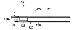
- the liquid crystal display unit 102 provided in the electronic device has a wide frame area C outside the liquid crystal active area A
- a liquid crystal display panel using the wide frame area C is used.
- the backlight 130 was attached to 122 with a frame-like double-sided tape 123.
- an optical sheet 125 composed of one or more backlights 130 is fixed to the front side of the backlight 130 by the frame-like double-sided tape 123.
- the backlight 130 has a light guide plate 126 in the backlight holder 129, and the back side is covered with a reflection plate 127.
- the backlight holder 129 has a sufficient adhesion area D, as shown in FIG. 7B, the most liquid crystal display panel 122 side of the optical sheet 125 can be attached to the backlight holder 129.
- the LED 128 as the light source is fixed with the backlight holder 129 as a reference.
- the backlight effective light-emitting area B needs to be larger than the liquid crystal active area A in order to shine light on the whole.
- the backlight holder 129 must be made larger than the liquid crystal display panel 122 in order to secure the bonding area D, and even if the frame range of the liquid crystal display panel 122 itself is narrowed, the entire electronic device is Has a problem that the frame region C becomes wide.
- Patent Document 1 it is known that the entire laminated body is covered with an optical adhesive film including the side surface from the front side in a state where the liquid crystal panel, the polarizing plate, and the backlight are laminated.
- belt-shaped packaging member are only joined by the end surface of the short side of an optical element laminated body, and other parts are only wrapped with a packaging member.
- the packaging member and the optical element laminate wrapped with the packaging member cannot be brought into close contact with each other, and the optical element laminate may move inside the packaging member. is there.
- the present invention has been made in view of such a point, and an object thereof is to achieve a narrow frame of the liquid crystal display unit with a simple and easy-to-assemble structure.
- the backlight is wrapped with an optical fixing sheet attached to the back surface of the liquid crystal display unit.
- the electronic device on the premise of an electronic device having a liquid crystal display unit, A rectangular plate-shaped liquid crystal display panel; An optical fixing sheet whose front side is attached to the back of the liquid crystal display panel; A rectangular plate-like backlight fixed in a state where the front surface is in contact with the back surface of the optical fixing sheet,
- the optical fixing sheet has extensions extending around the back side periphery of the backlight, and the extensions are formed on four sides of the optical fixing sheet in a state of being attached to the back of the liquid crystal display panel. It is affixed to the periphery of the four sides on the back side of the backlight.
- the entire display area can be illuminated without expanding the frame area even when a liquid crystal display unit with a narrow frame is used. it can.
- the backlight is wrapped with the optical fixing sheet attached to the back surface of the liquid crystal display unit rather than being wrapped with the optical fixing sheet from the front side of the liquid crystal display unit, a decrease in transmittance can be avoided. Since the back surface of the liquid crystal display unit is affixed with an optical fixing sheet, it is difficult for dust to enter between the back surface of the liquid crystal display unit and the backlight.
- each component constituting the backlight since the extension is attached to all the four side edges on the back side of the backlight, each component constituting the backlight does not shift in any direction. By doing so, the positional accuracy of each component is improved, the strength is increased, and it is difficult for dust to enter the gaps between the components.
- a liquid crystal display panel and The backlight can be securely held while maintaining the optical characteristics.
- the optical fixing sheet is provided with the extension that goes around the four sides of the back side of the backlight, and the extension is connected to the back of the liquid crystal display panel.
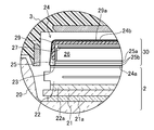
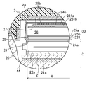
- FIG. 3 is an enlarged sectional view taken along a line II in FIG. 2 and a partially enlarged view thereof.
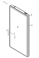
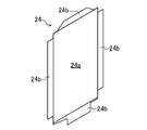
- 1 is a perspective view showing a mobile phone according to an embodiment of the present invention. It is a disassembled perspective view of a mobile phone. It is the perspective view which looked at the liquid crystal display part and the backlight from the back. It is a perspective view which shows the sheet
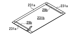
- FIG. 3 is a view corresponding to FIG. 1 according to Embodiment 2 of the present invention. It is the FIG. 1 equivalent view which concerns on the modification of Embodiment 2 of this invention. It is a perspective view which shows before folding the transparent sheet for backlights. It is a perspective view which shows the middle of folding the transparent sheet for backlights. It is a perspective view which shows after folding the transparent sheet for backlights.
- the mobile phone 1 as the electronic apparatus includes, for example, a front side cabinet 3 in which the liquid crystal display unit 2 is accommodated on the front side, and a back side covering the back side.
- a cabinet 4 and a rear cover 5 covering the back surface of the cabinet 4 are provided.
- a rechargeable battery 6 and a main board 7 are accommodated between the front side cabinet 3 and the back side cabinet 4.
- the liquid crystal display unit 2 includes a front cover 20 made of a glass plate, an acrylic plate, or the like that covers the front side.
- the front cover 20 has an outer peripheral edge extending toward the back side, but may be flat.
- a touch panel 21 is attached to the back side of the front cover 20.
- the touch panel 21 may not be provided.
- the touch panel 21 may also serve as the front cover 20.
- a rectangular plate-like liquid crystal display panel 22 is attached to the back side of the touch panel 21.
- the liquid crystal display panel 22 includes, for example, a printed circuit board in which a liquid crystal layer is sandwiched between a color filter substrate and an array substrate, front and back surfaces are covered with a polarizing plate, and a driving LSI is included. ing. As shown in FIGS. 1 and 4, a backlight 30 is fixed to the back surface of the liquid crystal display panel 22 by an optical fixing sheet 24 having a high light transmittance.
- the optical fixing sheet 24 is fixed to the back surface of the liquid crystal display panel 22 by a rectangular transparent optical adhesive tape 23 (OCA) having a high light transmittance, and the backlight 30 is the optical fixing sheet 24.
- OCA transparent optical adhesive tape 23
- the liquid crystal display panel 22 is fixed in a state where the front surface is in contact with the back surface.
- the optical fixing sheet 24 has a colorless and transparent film-like base material having a thickness of, for example, 10 to 250 ⁇ m, such as PET resin (polyethylene terephthalate) or PEN resin (polyethylene naphthalate). It has features such as high light transmittance, small difference in transmittance depending on wavelength, and thinness and strength.
- the optical fixing sheet 24 plays a role of transmitting the light of the backlight 30 to the liquid crystal display panel 22 side without loss or fixing the liquid crystal display panel 22 and the backlight 30 securely.
- a sheet (a part of a diffusion sheet or a lens sheet) having irregularities formed on the surface may be used. When the surface of the optical fixing sheet 24 has irregularities, there is an advantage that generation of Newton rings can be prevented.
- the rectangular main-body part 24a of a film base material is affixed on the back surface of the liquid crystal display panel 22 with the transparent optical adhesive tape 23.
- FIG. By making this base material thinner, the overall thickness is reduced.
- the base material includes a flap-shaped extension 24 b that can be bent on four sides.
- the backlight 30 includes a thin-walled bezel 29 made of a rectangular dish-shaped resin molded product, a metal molded product, or the like. On the bezel 29, there is provided a reflection sheet 27 and a backlight substrate 28 on which LEDs as light emitters are arranged with a space therebetween. A light guide plate 26 having a rectangular plate shape is disposed in a bezel 29 on the front side of the reflection sheet 27 and the backlight substrate 28.
- the reflection sheet 27 has, for example, a multilayer structure of a polyester resin base material. For example, silver is deposited on a PET (polyester resin) film, or a laminate of a PET (polyester resin) film and a metal foil such as aluminum. It is formed by configuring.
- the reflection sheet 27 has a thickness of, for example, 30 to 300 ⁇ m, has a high reflectance, has a small loss during reflection, reflects light emitted in a direction opposite to the liquid crystal display panel 22, and reflects the liquid crystal display panel. By sending it back to the side 22, it plays a role of reducing light loss and improving the luminance of the liquid crystal display unit 2.
- an extension fixing double-sided tape 29a is attached to the periphery of the backside of the bezel 29 of the backlight 30 at a portion where the extension 24b is attached.
- the extension 24b is affixed by the extension part fixing double-sided tape 29a.
- this extension part 24b may be affixed with the adhesive agent.
- a backlight transparent sheet 31 having a high light transmittance is provided on the back side of the main body 24a.
- the backlight transparent sheet 31 is made of a material having a high light transmittance, such as a PET film or a PEN film, and has a thickness of, for example, 10 to 250 ⁇ m.
- the backlight transparent sheet 31 has a small difference in transmittance depending on the wavelength, is thin and strong, is colorless and transparent, and has a flat surface, and transmits the light of the backlight 30 to the liquid crystal display panel 22 side without loss. It plays a role of securely holding the backlight 30.
- the backlight transparent sheet 31 a sheet (a part of a diffusion sheet or a lens sheet) having an uneven surface may be used.
- the backlight transparent sheet 31 is formed as a diffusion sheet having irregularities on the surface to prevent the generation of Newton rings.
- the backlight transparent sheet 31 is bent to the back side of the bezel 29 and attached on all four sides by the transparent sheet double-sided tape 29 b shown in FIG. 1 and the like.
- the backlight 30 can be assembled after the unit is assembled and inspected in advance.
- the backlight 30 is covered with a backlight transparent sheet 31 so that the diffusion sheet 25a contacts the front side of the light guide plate 26 and further the lens sheet 25b contacts the front side.
- the base material of the diffusion sheet 25a for example, a film-like or plate-like material such as polymethyl methacrylate, polycarbonate, polyvinyl chloride, polyester, acetate resin or the like can be considered.
- a light diffusing layer is formed on the substrate by coating.
- the diffusion sheet 25a has a thickness of, for example, 30 to 150 ⁇ m, has a high light transmittance, and is a translucent film (sheet or plate) that scatters and diffuses light.
- the diffusion sheet 25a plays a role of improving the luminance in the front direction while giving a wide viewing angle, and uniformly transmitting light from the light source to the entire surface of the liquid crystal display panel 22.
- the lens sheet 25b is made of, for example, an optical film obtained by molding a prism pattern of acrylic resin or photopolymer on the surface of polyester having excellent transparency, and the thickness thereof is, for example, 40 to 400 ⁇ m.
- the lens sheet 25b has a high light transmittance, and is incorporated in the front surface of the backlight 30 to collect the light emitted from the light source toward the user of the mobile phone 1 and improve the brightness on the front (orthogonal). In the case of using two sheets), the light that is not used outside the viewing angle is recycled by re-reflection and condensed in the direction of the user.
- the optical sheet 25 needs not to be bonded to the front surface of the light guide plate 26 and the back surface of the backlight transparent sheet 31 in the effective light emitting area of the backlight 30 in order to maintain the optical effect (light collection, diffusion, etc.). Become.
- the illumination range by the backlight 30 is indicated by X. This illumination range X is wider than the liquid crystal active area A.
- the touch panel 21 is attached to the back surface of the front cover 20 via the touch panel OCA 21a.
- liquid crystal display panel 22 is attached to the back surface of the touch panel 21 via the LCD OCA 22a.
- the front surface of the optical fixing sheet 24 is attached to the back surface of the liquid crystal display panel 22 with the transparent optical adhesive tape 23.
- the optical sheet 25 laminated in advance may be pasted outside the effective light emitting area of the backlight 30 on the back side of the main body 24 a of the optical fixing sheet 24.
- the optical sheet 25 may be attached to the light guide plate 26 side outside the effective light emitting area, or may be in a state where it is only positioned by the bezel 29 or the like.
- the optical sheet 25 may not be provided on the back side of the main body 24 a of the optical fixing sheet 24.
- the backlight 30 is prepared in a state where it is wrapped in the backlight transparent sheet 31 in a unit assembled state in advance.
- the backlight 30 assembled as a unit is pressed against the back surface of the optical fixing sheet 24 and positioned. At this time, the front surface of the backlight 30 is pressed against the optical fixing sheet 24.
- the base material itself of the optical fixing sheet 24 does not have adhesiveness, positioning is easy.
- the four extension portions 24b of the optical fixing sheet 24 are bent to the back side of the bezel 29, and attached to the back side four-side periphery with the extension portion fixing double-sided tape 29a.
- This configuration eliminates the need for bonding using the frame of the backlight holder as in the prior art, so the entire display area can be expanded without expanding the frame area even when the liquid crystal display unit 2 having a narrow frame is used. Can shine. Further, since the backlight 30 is wrapped with the optical fixing sheet 24 attached to the back surface of the liquid crystal display unit 2 instead of being wrapped with the optical fixing sheet 24 from the front side of the liquid crystal display unit 2, the transmittance decreases. Can be avoided.
- the diffusion sheet 25a and the lens sheet 25b and the front side of the light guide plate 26 and the back side of the backlight transparent sheet 31 are not bonded within the effective light emitting area (illumination range X) of the backlight 30, Light collection and diffusion on the front side of the light 30 is not hindered.
- the light guide plate 26 can be arranged to fill the side wall of the bezel 29 and there is no need to provide a pasting area as in the conventional case, the backlight 30 with a narrow frame can be obtained.
- the extension part 24b is affixed to all the four-side rims on the back side of the backlight 30, the optical sheet 25, the diffusion sheet 25a, the lens sheet 25b, the light guide plate 26, the reflection sheet 27, etc. are shifted in any direction. There is nothing. By doing so, the positional accuracy of each component is improved, the strength is increased, and it is difficult for dust to enter the gaps between the components.
- the optical fixing sheet 24 is bonded using the back surface of the backlight 30 having high rigidity on the front side of the extension 24b of the optical fixing sheet 24, instead of bonding the optical fixing sheets 24 to each other.
- the liquid crystal display panel 22 and the backlight 30 can be reliably held while maintaining the optical characteristics.
- a narrow frame of the liquid crystal display unit 2 can be achieved with a simple and easy-to-assemble structure.
- FIG. 8 shows a second embodiment of the present invention, which differs from the first embodiment in that there is no bezel 29.
- the same portions as those in FIGS. 1 to 6 are denoted by the same reference numerals, and detailed description thereof is omitted.
- the outer shapes of the light guide plate 26 and the optical sheet 25 can be made larger than those of the first embodiment as long as the backlight 30 has the same outer shape. For this reason, the illumination range X ′ is wider than the illumination range X of the first embodiment.
- the thickness may be increased or a laminated material with a rigid member such as a sheet metal may be used.
- Embodiment 2- 9 to 10C show modifications of the second embodiment of the present invention, and the shape and fixing method of the backlight transparent sheet 231 are different from those of the first embodiment.
- the backlight transparent sheet 31 is bonded to the periphery of the four sides on the back side of the bezel 29 with the transparent sheet double-sided tape 29b, but in this modification, the backlight transparent sheet 231 is On one side in the longitudinal direction, an additional extension 231b is provided which extends greatly to the other shorter extension 231a side.
- the additional extension 231b is bonded to the extension 231a so as to overlap each other. That is, after the additional extension 231b is pasted with the double-sided tape 29b for transparent sheet, the extension 231a is pasted with the double-sided tape 29b for transparent sheet so as to overlap the additional extension 231b previously pasted. Yes.
- the additional extension portion 231b may be pasted to the extension portion 231a.
- the optical fixing sheet 24 is just to affix the optical fixing sheet 24 with the same thing as the said Embodiment 1 with the double-sided tape 29a for extension part fixation.
- the burden on the reflective sheet 27 to which the transparent sheet double-sided tape 29b is attached can be reduced, and the components inside the backlight transparent sheet 231 can be closely fixed so that they do not wobble. It is not necessary to increase the rigidity of the reflection sheet 27 more than necessary.
- the present invention may be configured as follows with respect to the above embodiment.
- the backlight 30 is formed by the optical fixing sheet 24 without using the backlight transparent sheet 31. May be covered.
- the optical sheet 25 is preferably attached to the back side of the main body 24 a of the optical fixing sheet 24. In this embodiment, there is no effect such as ease of handling by unitizing the backlight 30, but the number of parts can be reduced and the thickness can be reduced by the absence of the backlight transparent sheet 31.
- the diffusion sheet 25a, the optical fixing sheet 24, and the backlight transparent sheet 31 may be a sheet having an uneven surface. By doing so, it is possible to prevent interference fringes from being generated in the liquid crystal display unit while maintaining the light diffusion function.
- the electronic device is the mobile phone 1, but it is a tablet terminal, PHS (Personal Handy-phone System), PDA (Personal Digital Assistant), personal computer, mobile tool, electronic dictionary, calculator, game machine, or the like.
- PHS Personal Handy-phone System
- PDA Personal Digital Assistant
- personal computer mobile tool, electronic dictionary, calculator, game machine, or the like.
- a small liquid crystal display, a liquid crystal television, a Blu-ray (DVD) recorder, or the like may be used.
Landscapes
- Physics & Mathematics (AREA)
- Nonlinear Science (AREA)
- General Physics & Mathematics (AREA)
- Optics & Photonics (AREA)
- Mathematical Physics (AREA)
- Chemical & Material Sciences (AREA)
- Crystallography & Structural Chemistry (AREA)
- Liquid Crystal (AREA)
- Planar Illumination Modules (AREA)
- Devices For Indicating Variable Information By Combining Individual Elements (AREA)
Abstract
Description
上記電子機器は、
矩形板状の液晶表示パネルと、
正面側が上記液晶表示パネルの背面に貼り付けられる光学固定用シートと、
上記光学固定用シートの背面に正面が当接した状態で固定される矩形板状のバックライトとを備え、
上記光学固定用シートは、上記バックライトの背面側周縁に回り込む延長部を有し、上記液晶表示パネルの背面に貼り付けられた状態で上記延長部が該光学固定用シートの四辺にそれぞれ形成されており、上記バックライトの背面側の四辺周縁に貼り付けられている。
図2及び図3に示すように、本実施形態に係る電子機器としての携帯電話機1は、例えば、正面側に液晶表示部2が収容される正面側キャビネット3と、その背面側を覆う背面側キャビネット4と、その背面を覆うリアカバー5とを備えている。正面側キャビネット3と背面側キャビネット4との間には、充電池6やメイン基板7が収容されている。
図8は本発明の実施形態2を示し、ベゼル29がない点で上記実施形態1と異なる。なお、本実施形態では、図1~図6と同じ部分については同じ符号を付してその詳細な説明は省略する。
図9~図10Cは本発明の実施形態2の変形例を示し、バックライト用透明シート231の形状及び固定方法が上記実施形態1と異なる。
本発明は、上記実施形態について、以下のような構成としてもよい。
2 液晶表示部
3 正面側キャビネット
4 背面側キャビネット
5 リアカバー
6 充電池
7 メイン基板
20 正面カバー
21 タッチパネル
21a タッチパネル用OCA
22 液晶表示パネル
22a LCD用OCA
23 透明光学粘着テープ
24 光学固定用シート
24a 本体部
24b 延長部
25 光学シート
25a 拡散シート
25b レンズシート
26 導光板
27 反射シート
28 バックライト用基板
29 ベゼル
29a 延長部固定用両面テープ
29b 透明シート用両面テープ
30 バックライト
31 バックライト用透明シート
231 バックライト用透明シート
231a 延長部
231b 追加延長部
Claims (5)
- 液晶表示部を有する電子機器において、
矩形板状の液晶表示パネルと、
正面側が上記液晶表示パネルの背面に貼り付けられる光学固定用シートと、
上記光学固定用シートの背面に正面が当接した状態で固定される矩形板状のバックライトとを備え、
上記光学固定用シートは、上記バックライトの背面側周縁に回り込む延長部を有し、上記液晶表示パネルの背面に貼り付けられた状態で上記延長部が該光学固定用シートの四辺にそれぞれ形成されており、上記バックライトの背面側の四辺周縁に貼り付けられている
ことを特徴とする電子機器。 - 請求項1に記載の電子機器において、
上記光学固定用シートは、接着性を有さない透明なフィルム状の基材を有し、該基材の矩形状の本体部の正面が接着剤又は両面テープで上記液晶表示パネルの背面に貼り付けられると共に、上記本体部の背面が上記バックライトの正面に当接し、かつ回り込んだ上記延長部が接着剤又は両面テープで上記バックライトの背面側周縁に貼り付けられている
ことを特徴とする電子機器。 - 請求項1又は2に記載の電子機器において、
上記バックライトは、矩形皿状のベゼル上に反射シートと発光体を有する基板とを有し、該反射シート及び基板の正面側に導光板が配置されており、
上記導光板の正面側が上記バックライトの正面側を包み込むバックライト用透明シートで覆われている
ことを特徴とする電子機器。 - 請求項3に記載の電子機器において、
上記バックライト用透明シートは、上記光学固定用シートに当接する部分に凹凸のあるシートである
ことを特徴とする電子機器。 - 請求項1から4までのいずれか1つに記載の電子機器を製造する方法において、
上記液晶表示パネルの背面に上記光学固定用シートの正面を接着剤又は両面テープにより貼り付け、
上記光学固定用シートの背面に上記バックライトを押し当て、
上記光学固定用シートの延長部を折り曲げて上記バックライトの背面側周縁に接着剤又は両面テープにより貼り付ける
ことを特徴とする電子機器の製造方法。
Priority Applications (2)
| Application Number | Priority Date | Filing Date | Title |
|---|---|---|---|
| US15/305,355 US20170045766A1 (en) | 2014-05-19 | 2015-05-14 | Electronic device and method for manufacturing same |
| JP2016520926A JP6205488B2 (ja) | 2014-05-19 | 2015-05-14 | 電子機器及びその製造方法 |
Applications Claiming Priority (2)
| Application Number | Priority Date | Filing Date | Title |
|---|---|---|---|
| JP2014-103569 | 2014-05-19 | ||
| JP2014103569 | 2014-05-19 |
Publications (1)
| Publication Number | Publication Date |
|---|---|
| WO2015177995A1 true WO2015177995A1 (ja) | 2015-11-26 |
Family
ID=54553678
Family Applications (1)
| Application Number | Title | Priority Date | Filing Date |
|---|---|---|---|
| PCT/JP2015/002449 Ceased WO2015177995A1 (ja) | 2014-05-19 | 2015-05-14 | 電子機器及びその製造方法 |
Country Status (3)
| Country | Link |
|---|---|
| US (1) | US20170045766A1 (ja) |
| JP (1) | JP6205488B2 (ja) |
| WO (1) | WO2015177995A1 (ja) |
Families Citing this family (1)
| Publication number | Priority date | Publication date | Assignee | Title |
|---|---|---|---|---|
| CN110764651B (zh) * | 2019-10-25 | 2022-05-13 | 业成科技(成都)有限公司 | 显示装置 |
Citations (3)
| Publication number | Priority date | Publication date | Assignee | Title |
|---|---|---|---|---|
| JP2003057649A (ja) * | 2001-08-15 | 2003-02-26 | Nec Corp | 透過型表示装置 |
| JP2006221058A (ja) * | 2005-02-14 | 2006-08-24 | Sony Corp | 表示装置 |
| JP2010122691A (ja) * | 2008-11-24 | 2010-06-03 | Samsung Electronics Co Ltd | 液晶表示装置 |
Family Cites Families (2)
| Publication number | Priority date | Publication date | Assignee | Title |
|---|---|---|---|---|
| US20130148381A1 (en) * | 2010-08-25 | 2013-06-13 | Sharp Kabushiki Kaisha | Display device |
| TWI503355B (zh) * | 2013-02-20 | 2015-10-11 | Lg Chemical Ltd | 顯示設備的封裝膜 |
-
2015
- 2015-05-14 US US15/305,355 patent/US20170045766A1/en not_active Abandoned
- 2015-05-14 WO PCT/JP2015/002449 patent/WO2015177995A1/ja not_active Ceased
- 2015-05-14 JP JP2016520926A patent/JP6205488B2/ja not_active Expired - Fee Related
Patent Citations (3)
| Publication number | Priority date | Publication date | Assignee | Title |
|---|---|---|---|---|
| JP2003057649A (ja) * | 2001-08-15 | 2003-02-26 | Nec Corp | 透過型表示装置 |
| JP2006221058A (ja) * | 2005-02-14 | 2006-08-24 | Sony Corp | 表示装置 |
| JP2010122691A (ja) * | 2008-11-24 | 2010-06-03 | Samsung Electronics Co Ltd | 液晶表示装置 |
Also Published As
| Publication number | Publication date |
|---|---|
| JP6205488B2 (ja) | 2017-09-27 |
| JPWO2015177995A1 (ja) | 2017-04-20 |
| US20170045766A1 (en) | 2017-02-16 |
Similar Documents
| Publication | Publication Date | Title |
|---|---|---|
| JP5222229B2 (ja) | 表示装置 | |
| JP5734145B2 (ja) | 面状照明装置 | |
| US20130242609A1 (en) | Surface light source device | |
| WO2016176929A1 (zh) | 背光模块及液晶显示器 | |
| CN102681255B (zh) | 显示装置 | |
| US9971086B2 (en) | Backlight module and liquid crystal display | |
| CN106773200B (zh) | 显示设备 | |
| TWI408445B (zh) | 觸控顯示裝置及其防護鏡片與組裝方法 | |
| JP2001272509A (ja) | 光拡散材および該光拡散材を用いる液晶表示装置 | |
| WO2016106898A1 (zh) | 胶框、背光模组以及液晶面板 | |
| CN104595802A (zh) | 一种背光模组及液晶显示器 | |
| KR101630342B1 (ko) | 액정 표시장치 및 그 조립방법 | |
| JP2017126553A (ja) | バックライト装置、およびこれを備える表示装置 | |
| JP6749795B2 (ja) | バックライト装置、これを備える表示装置、およびバックライト装置の製造方法 | |
| CN217588325U (zh) | 显示面板及显示装置 | |
| JP6205488B2 (ja) | 電子機器及びその製造方法 | |
| WO2015118813A1 (ja) | 液晶表示装置 | |
| JP2022023207A (ja) | 表示装置 | |
| CN106200113B (zh) | 背光模块 | |
| JP6266804B2 (ja) | 表示装置 | |
| JP2001117069A (ja) | 表示装置及び該表示装置に用いられる表示パネル | |
| JP6638439B2 (ja) | 面光源装置、表示装置、及び電子機器 | |
| CN212781605U (zh) | 背光模组及液晶显示装置 | |
| CN103488370B (zh) | 具有电磁触控模块的显示模块 | |
| WO2011161996A1 (ja) | 液晶表示装置 |
Legal Events
| Date | Code | Title | Description |
|---|---|---|---|
| 121 | Ep: the epo has been informed by wipo that ep was designated in this application |
Ref document number: 15795640 Country of ref document: EP Kind code of ref document: A1 |
|
| ENP | Entry into the national phase |
Ref document number: 2016520926 Country of ref document: JP Kind code of ref document: A |
|
| WWE | Wipo information: entry into national phase |
Ref document number: 15305355 Country of ref document: US |
|
| NENP | Non-entry into the national phase |
Ref country code: DE |
|
| 122 | Ep: pct application non-entry in european phase |
Ref document number: 15795640 Country of ref document: EP Kind code of ref document: A1 |