WO2015166360A1 - Synthesis of new small molecules/oligomers with high conductivity and absorption for optoelectronic application - Google Patents
Synthesis of new small molecules/oligomers with high conductivity and absorption for optoelectronic application Download PDFInfo
- Publication number
- WO2015166360A1 WO2015166360A1 PCT/IB2015/052215 IB2015052215W WO2015166360A1 WO 2015166360 A1 WO2015166360 A1 WO 2015166360A1 IB 2015052215 W IB2015052215 W IB 2015052215W WO 2015166360 A1 WO2015166360 A1 WO 2015166360A1
- Authority
- WO
- WIPO (PCT)
- Prior art keywords
- organic
- compound
- layer
- photovoltaic cell
- substrate
- Prior art date
- Legal status (The legal status is an assumption and is not a legal conclusion. Google has not performed a legal analysis and makes no representation as to the accuracy of the status listed.)
- Ceased
Links
- 0 CI(*c1c2)=C(*)*Nc1cc1c2cc(cc(*)c(*C(*)C(C(C(C(N=*)=C2N)=C(*)*C3CC3)=*)=C2N)c2)c2c1C#Cc1c(cc(*)c(**C(*)C(/C(/C([C@@](C2N)N=C)=*CCC3)=*/C=C3I=C)=C2N)c2)c2cc2c1cc(CC1I=C(*)*1CI1)c1c2 Chemical compound CI(*c1c2)=C(*)*Nc1cc1c2cc(cc(*)c(*C(*)C(C(C(C(N=*)=C2N)=C(*)*C3CC3)=*)=C2N)c2)c2c1C#Cc1c(cc(*)c(**C(*)C(/C(/C([C@@](C2N)N=C)=*CCC3)=*/C=C3I=C)=C2N)c2)c2cc2c1cc(CC1I=C(*)*1CI1)c1c2 0.000 description 3
Classifications
-
- C—CHEMISTRY; METALLURGY
- C07—ORGANIC CHEMISTRY
- C07D—HETEROCYCLIC COMPOUNDS
- C07D495/00—Heterocyclic compounds containing in the condensed system at least one hetero ring having sulfur atoms as the only ring hetero atoms
- C07D495/02—Heterocyclic compounds containing in the condensed system at least one hetero ring having sulfur atoms as the only ring hetero atoms in which the condensed system contains two hetero rings
- C07D495/04—Ortho-condensed systems
-
- C—CHEMISTRY; METALLURGY
- C07—ORGANIC CHEMISTRY
- C07F—ACYCLIC, CARBOCYCLIC OR HETEROCYCLIC COMPOUNDS CONTAINING ELEMENTS OTHER THAN CARBON, HYDROGEN, HALOGEN, OXYGEN, NITROGEN, SULFUR, SELENIUM OR TELLURIUM
- C07F7/00—Compounds containing elements of Groups 4 or 14 of the Periodic Table
- C07F7/02—Silicon compounds
- C07F7/08—Compounds having one or more C—Si linkages
- C07F7/0803—Compounds with Si-C or Si-Si linkages
- C07F7/081—Compounds with Si-C or Si-Si linkages comprising at least one atom selected from the elements N, O, halogen, S, Se or Te
- C07F7/0812—Compounds with Si-C or Si-Si linkages comprising at least one atom selected from the elements N, O, halogen, S, Se or Te comprising a heterocyclic ring
-
- H—ELECTRICITY
- H10—SEMICONDUCTOR DEVICES; ELECTRIC SOLID-STATE DEVICES NOT OTHERWISE PROVIDED FOR
- H10K—ORGANIC ELECTRIC SOLID-STATE DEVICES
- H10K10/00—Organic devices specially adapted for rectifying, amplifying, oscillating or switching; Organic capacitors or resistors having potential barriers
- H10K10/40—Organic transistors
- H10K10/46—Field-effect transistors, e.g. organic thin-film transistors [OTFT]
-
- H—ELECTRICITY
- H10—SEMICONDUCTOR DEVICES; ELECTRIC SOLID-STATE DEVICES NOT OTHERWISE PROVIDED FOR
- H10K—ORGANIC ELECTRIC SOLID-STATE DEVICES
- H10K30/00—Organic devices sensitive to infrared radiation, light, electromagnetic radiation of shorter wavelength or corpuscular radiation
- H10K30/30—Organic devices sensitive to infrared radiation, light, electromagnetic radiation of shorter wavelength or corpuscular radiation comprising bulk heterojunctions, e.g. interpenetrating networks of donor and acceptor material domains
-
- H—ELECTRICITY
- H10—SEMICONDUCTOR DEVICES; ELECTRIC SOLID-STATE DEVICES NOT OTHERWISE PROVIDED FOR
- H10K—ORGANIC ELECTRIC SOLID-STATE DEVICES
- H10K85/00—Organic materials used in the body or electrodes of devices covered by this subclass
- H10K85/40—Organosilicon compounds, e.g. TIPS pentacene
-
- H—ELECTRICITY
- H10—SEMICONDUCTOR DEVICES; ELECTRIC SOLID-STATE DEVICES NOT OTHERWISE PROVIDED FOR
- H10K—ORGANIC ELECTRIC SOLID-STATE DEVICES
- H10K85/00—Organic materials used in the body or electrodes of devices covered by this subclass
- H10K85/60—Organic compounds having low molecular weight
- H10K85/649—Aromatic compounds comprising a hetero atom
- H10K85/655—Aromatic compounds comprising a hetero atom comprising only sulfur as heteroatom
-
- H—ELECTRICITY
- H10—SEMICONDUCTOR DEVICES; ELECTRIC SOLID-STATE DEVICES NOT OTHERWISE PROVIDED FOR
- H10K—ORGANIC ELECTRIC SOLID-STATE DEVICES
- H10K85/00—Organic materials used in the body or electrodes of devices covered by this subclass
- H10K85/60—Organic compounds having low molecular weight
- H10K85/649—Aromatic compounds comprising a hetero atom
- H10K85/657—Polycyclic condensed heteroaromatic hydrocarbons
- H10K85/6576—Polycyclic condensed heteroaromatic hydrocarbons comprising only sulfur in the heteroaromatic polycondensed ring system, e.g. benzothiophene
-
- H—ELECTRICITY
- H10—SEMICONDUCTOR DEVICES; ELECTRIC SOLID-STATE DEVICES NOT OTHERWISE PROVIDED FOR
- H10K—ORGANIC ELECTRIC SOLID-STATE DEVICES
- H10K30/00—Organic devices sensitive to infrared radiation, light, electromagnetic radiation of shorter wavelength or corpuscular radiation
- H10K30/50—Photovoltaic [PV] devices
-
- Y—GENERAL TAGGING OF NEW TECHNOLOGICAL DEVELOPMENTS; GENERAL TAGGING OF CROSS-SECTIONAL TECHNOLOGIES SPANNING OVER SEVERAL SECTIONS OF THE IPC; TECHNICAL SUBJECTS COVERED BY FORMER USPC CROSS-REFERENCE ART COLLECTIONS [XRACs] AND DIGESTS
- Y02—TECHNOLOGIES OR APPLICATIONS FOR MITIGATION OR ADAPTATION AGAINST CLIMATE CHANGE
- Y02E—REDUCTION OF GREENHOUSE GAS [GHG] EMISSIONS, RELATED TO ENERGY GENERATION, TRANSMISSION OR DISTRIBUTION
- Y02E10/00—Energy generation through renewable energy sources
- Y02E10/50—Photovoltaic [PV] energy
- Y02E10/549—Organic PV cells
Definitions
- the invention generally concerns small molecules and oligomers based on an anthradithiophene core combined with conjugated oligomer side groups comprising Group 16 elements sulfur, selenium, or tellurium, or combinations thereof. These compounds have electron rich and electron deficient regions and can be used in organic electronic applications.
- conjugated organic polymers have found widespread use in organic electronic devices including organic light emitting diodes (OLEDs), organic photovoltaics (OPVs) and organic field effect transistors (OFETs), their small molecule/oligomer counterparts have not.
- OLEDs organic light emitting diodes
- OFETs organic field effect transistors
- polymers have continuous ⁇ - electron systems, and consequent electron-transport properties make them ideal candidates for a variety of electronic devices.
- Strategic chemical modification of different polymer moieties with varying electron-rich and electron-poor functionalities allows these electron- transporting molecules to be "tuned" for specific applications.
- the present invention offers a solution to the aforementioned problems associated with both current polymer-based as well as small-molecule and oligomer-based electronics.
- the solution is premised on a donor-acceptor (D-A) when creating small molecules or oligomers of the present invention, which can be semiconducting or conducting molecules or oligomers.
- D-A donor-acceptor
- the small molecules and oligomers of the present invention have been shown to have low band gap semiconducting properties due to the presence of a deloeal zed ⁇ -electron system comprising electron-rich (donor) and electron- deficient (acceptor) units.
- the donor unit comprises an anthradithiophene core.
- the acceptor unit utilizes group 16 elements (S, Se, or Te, or any combination or all thereof— e.g., S and S, S and Se, S and Te, Se and Se and Se, Se and Te, or Te and Te, etc. ) to allow for improved light absorption properties and enhanced electronic properties, including increased charge carrier mobility.
- group 16 elements S, Se, or Te, or any combination or all thereof— e.g., S and S, S and Se, S and Te, Se and Se and Se, Se and Te, or Te and Te, etc.
- the light absorption properties of the small molecules and oligomers of the present invention can be extended into the ultraviolet and near infrared regions of solar radiation, which allows for increased efficiency as well as fabrication of visibly transparent solar cells. Additional advantages of the small molecules and oligomers of the present invention include: straight forward synthesis, scalable reaction and purification
- the compounds and oligomers of the present invention can have an overall flat planar stmcture, which allows for acceptable conjugation lengths.
- R 2 and R' can each independently be
- R 4 can be
- Z , or Zi and Z 2 or Z 3 and Z 4 or Z 5 and Z 6 are each N and are connected by a metal bridge atom to form, together with the carbon atoms to which they are attached, a 5 member ring system;
- R 2 o and R 2 i are each independently a linear, branched or cyclic aliphatic, aiyl or heteroaiyl group of up to 20 carbon atoms: z can be an integer from 0 to 5; and n can be an integer from 0 to 5.
- the curved lines spanning the X f , C, and Y f atoms and the X 2 , C, and Y 2 atoms represent double bonds that can either be present between X' and C or C and Y 3 and between X and C or C and Y 2 .
- M 1 is S and M 2 is S
- M 1 is S and M 2 is Se
- M' is S and M" is Te
- M 1 is Se and M 2 is Se or M' is Se and M 2 is Te.
- M 1 is Te and IVP is Te.
- the number and combination of group 16 elements can be selected to achieve a desired result.
- Such a selection process allows for wider flexibility and tunability in obtaining desired band gaps.
- the compound can have the following structure:
- the compound can have the following structure:
- M ' is S, Se, or Te
- M 5 is S, Se, or Te
- the compound can have the following structure:
- the compound in siili another embodiment, can have the following stmcture:
- the compound can have one of the following structures
- any of the compounds of the present invention can be purified or isolated by techniques known to those of skill in the art (e.g., filtration, precipitation, steam distillation, distillation evaporation, sublimation, centiifugation, decantation, or the like).
- the purified or isolated compound can be in a dry or powdered form or can be stored within a liquid.
- the produced compound can be further modified with a dopant so as to enhance its p-type or n- type properties.
- the produced compounds can be conductive or semi-conductive compounds and can be used in such electronic applications and devices.
- the compounds (e.g., small molecules and oligomers) of the present invention can be used in electronic applications. These compounds can be used in an active layer of an electronic device.
- the active layer can be an organic or hybrid semiconducting or conducting layer.
- the device can include a substrate, the photoactive layer, and at least two electrodes, one of which is transparent, wherein at least a portion or all of the photoactive layer is disposed between said electrodes.
- the transparent electrode can be a cathode and the other electrode can be an anode.
- the transparent electrode can be an anode and the other electrode can be a cathode. In some instances both of the aforementioned electrodes can be transparent.
- one of the electrodes can be transparent while the other is non-transparent (e.g., opaque) or reflective, such that it can reflect electromagnetic radiation such as ultraviolet light or visible light or sun light.
- the substrate can be opaque, reflective, or transparent.
- the electronic device can be a photovoltaic cell or can include a photovoltaic cell. Said cell may not include an electrolyte.
- the photovoltaic cell can be designed such that it is a single active layer or bi-layer photovoltaic ceil .
- a bulk-heteroj unction layer can be produced by using the compounds of the present invention alone or in combination with known small molecule, oligomers, or polymers, or combinations thereof.
- the photovoltaic cell can be included in an organic electronic device.
- OLEDs organic light-emitting diodes
- PLEDs polymeric organic light-emitting diodes
- SM- OLEDs small-molecule organic light-emitting diodes
- O-ICs organic integrated circuits
- OFETs organic field effect transistors
- OFTs organic thin film transistors
- O-SCs organic solar cell
- Q-iasers organic laser diodes
- the process can include disposing said semiconducting or conducting layer on said substrate or said electrode.
- the semiconducting layer can be photoactive.
- the conducting layer can be photoactive.
- the substrate can be rigid or flexible.
- the substrate can include an electrode and the photoactive layer can be disposed on said electrode.
- the substrate may not include an electrode, and the photoactive layer can be disposed on the substrate.
- the substrate can include an electrode and the photoactive layer can be disposed on the subsirate or the electrode or onto both.
- Deposition of said layer can be by spray coating, ultra sonic spray coating, roll-to-roil coating, drop casting, dip coating, Mayer rod coating, gravure coating, slot die coating, doctor blade coating, spin coating, meniscus coating, transfer printing, ink-jet printing, offset printing or screen printing process.
- deposition of said layer can be by vacuum deposition or organic vapor phase deposition (OVPD), solution precipitation, organic molecular beam deposition, or vacuum thermal evaporation (VTE).
- OVPD organic vapor phase deposition
- VTE vacuum thermal evaporation
- a linear aliphatic group is a substituted or un substituted, saturated hydrocarbon with no tertiary or quaternary carbons.
- Aliphatic group substituents include, but are not limited to halogen, hydroxy!, alkyoxy, haloalkyl, haloaikoxy, carboxyiic acid, ester, amine, amide, nitrile, acvi, thiol and thioether.
- a branched aliphatic group is a substituted or nsubstituted, saturated hydrocarbon that includes at least one tertiary and/or quaternary carbon.
- Branched aliphatic group substituents include, but are not limited to alkyl, halogen, hydroxy!, alkyoxy, haloalkyl, haloaikoxy, carboxyiic acid, ester, amine, amide, nitrile, acyl, thiol and thioether.
- a cyclic aliphatic group is a substituted or unsubstituted, saturated, hydrocarbon that includes at least one ring in its structure.
- Polycyciic aliphatic groups may include fused, e.g., decalin, and/or spiro, e.g., spiro[5.5]undecane, polycyciic groups.
- Cyclic aliphatic group substituents include, but are not limited to aikyi, halogen, hydroxvl, alkvoxy, haloalkvl, haloalkoxy, carboxylic acid, ester, amine, amide, nitrile, acyl, thiol and thioether.
- An aryl group is a substituted or unsubstituted, mono- or polycyciic hydrocarbon with alternating single and double bonds within each ring structure.
- Aryl group substituents include, but are not limited to alkvl, halogen, hydroxy!, alkyoxv, haloalkvl, haloalkoxy, carboxylic acid, ester, amine, amide, nitrile, acyl, thiol and thioether.
- a heteroaryl group is a mono-or polycyciic hydrocarbon with alternating single and double bonds within each ring structure, and at least one atom within at least one ring is not carbon.
- Heteroaryl group substituents include, but are not limited to alky I, halogen, hydroxyl, alkvoxy, haioalkyl, haloalkoxy, carboxylic acid, ester, amine, amide, nitrile, acyl, thiol and thioether.
- Aromatic group is a substituted or unsubstituted, mono- or polycyciic hydrocarbon with alternating single and double bonds within each ring structure.
- Aromatic group substituents include, but are not limited to alkyl, halogen, hydroxy!, alkyoxv, haioalkyl, haloalkoxy, carboxylic acid, ester, amine, amide, nitrile, acyl, thiol and thioether.
- a hetero-aromatic group is a mono-or polycyciic hydrocarbon with alternating single and double bonds within each ring structure, and at least one atom within at least one ring is not carbon.
- Hetero-aromatic group substituents include, but are not limited to alkyl, halogen, hydroxyl, alkyoxv, haioalkyl, haloalkoxy, carboxylic acid, ester, amine, amide, nitrile, acyl, thiol and thioether.
- Alkyl group is linear or branched, substituted or unsubstituted, saturated hydrocarbon.
- Alkyl group substituents may include, but are not limited to alkyl, halogen, hydroxyl, alk oxy, haioalkyl, haloalkoxy, carboxylic acid, ester, amine, amide, nitrile, acyl, thiol and thioether.
- the compounds and related processes of making and using said compounds, the photoactive layers, the photovoltaic cells, and the organic electronic devices of the present invention can "comprise,” “consist essentially of,” or “consi st of” particular ingredients, components, compounds, compositions, etc. disclosed throughout the specification.
- a basic and novel characteristic of the aforesaid compounds are their light absorption and charge carrier mobility properties.
- FIG. It Illustration of an organic photovoltaic cell incorporating the small molecules or oligomers or polymers or all types of the present invention.
- FIGS. 2A-B Thermal ellipsoid plots of compound 6.
- FIGS. 3A-C Scanning electron microscopy (SEM) images of QuIS-S crystals suspended on standard transmission electron microscopy (TEM) grids.
- FIG. 4 XRD of QuIS-S prepared under different conditions.
- FIGS. 5A-D Atomic Force Microscopy (AFM) images showing the determination of thickness of films of QuIS-S and QuIS-Se on glass.
- AFM Atomic Force Microscopy
- FIG. 6 UV-Vis spectra of both QuIS-S and QuIS-Se films.
- FIGS. 7 Tauc plots for QuIS-S and QuiS-Se films.
- FIG. 8 Ultraviolet photoelectron spectroscopy (UPS) for QuIS-S and QuIS-Se films.
- FIG. 9i Proposed band diagram for both QuIS-S and QuIS-Se.
- FIG. 10 Illustration of a bilayer OPV using a QulS-S film and a PC71 BM film .
- the present invention offers a solution to the problems associated with current small molecules and oligomers that are used in organic electronic devices.
- the solution resides in the creation of small molecules or oligomers that have low band gap semiconducting properties due to the presence of a delocalized ⁇ -electron system that has an electron rich (donor) anthradithiophene core and an electron-deficien (acceptor) unit having group 16 elements such as sulfur, selenium, or tellurium.
- the compounds and oligomers have good light absorption and electronic properties, including increased charge carrier mobility.
- the compounds of the present invention can be prepared as small molecules or oligomers that contain a central electron rich monomelic unit (or electron donor unit) or units in instances where oligomers or polymers are concerned that have an electron rich monomelic unit that is connected to at least one or two comparatively electron deficient monomelic unit or units (or electron acceptor units) that feature group 16 heteroatoms of sulfur, selenium, or tellurium or combinations thereof.
- the compounds and oligomers can be semi-conductive or conductive. Larger units are also contemplated and can be prepared to achieve a desired compound or oligomer. Further each small molecule or oligomer can be terminated with a thiophene capping unit.
- the following provides non-limiting schemes that can be used to prepare small molecules and oligomers of the present invention.
- the small molecules and oligomers can be modified with additional non-functional or functional groups as desired.
- the small molecules and oligomers can be soluble in common organic solvents, examples of which are provided below, and are stable for extended periods of time under ambient conditions.
- reaction scheme 1 illustrates a non-limiting process to make monomeric electron acceptor units that can be used with the small molecules and oligomers of the present invention:
- excess (5-10) of equivalent Na[BH 4 ] can be used to synthesize compound A.
- compounds B L B2, B3 are attached directly to an electron donor unit by using the processes described throughout this specification or processes known to those of ordinary skill in the art.
- each of compounds B l, B2, and B3 can be linked together to create small oligomers (e.g., the oligomers contain up to 5 monomelic units (i.e., n can be an integer of L 2, 3, 4, or 5 or more).
- This oligomerization step can be performed by using well established coupling reactions such as Suzuki coupling where compounds B l, B2, and/or B3 are coupled with a boronic acid or boronic ester containing moiety.
- the desired coupling reaction can also be carried out using Stilie coupling when compounds B l, B2, and/or B3 are reacted with a tin containing organic moiety to produce compounds B4, B5, and B6
- the reaction can be performed under Suzuki coupling reaction conditions and the catalyst Pd(P! 3 h ;) ;.
- solvent (toluene) and activator (Na 2 C0 3 ) can vary depending on the reaction. In some cases, different sets of catalysts, solvents and activators can be used. Also the percentage of product formation can change by modifying these parameters.
- the small molecule or oligomer can be terminated with an aromatic, hetero-aromatic, or alkyl functional group rather than with a thiophene capping unit.
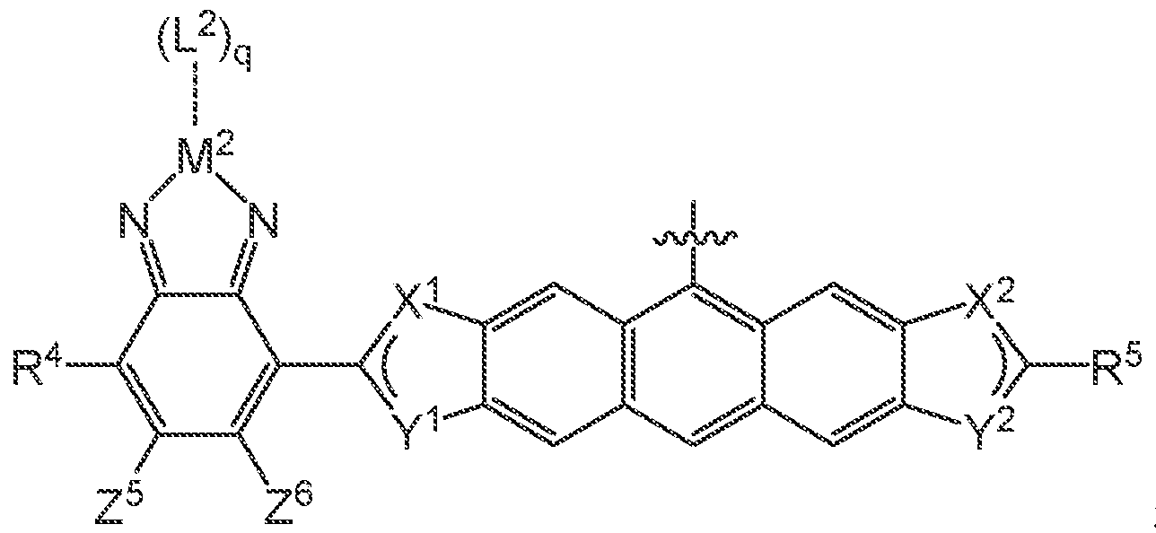
- R 9 , R 1 , R l ⁇ R 12 , R lj , and Z 1 and Z 2 groups are defined above in the summary of the invention section and in the claims, the definitions of which are incorporated into this section by reference.
- the CI , C2, C3, €4, C5, and C6 compounds can then be covalently linked to an electron donor unit.
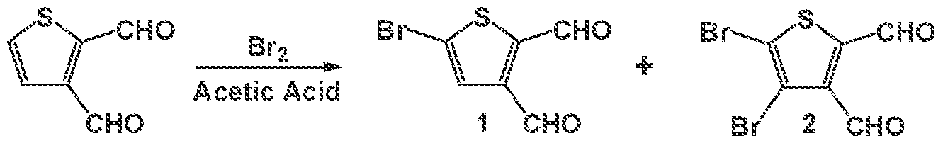
- Reaction scheme 3 provides a non-limiting process to make an electron donor unit that can be used with the molecules and oligomers of the present invention.
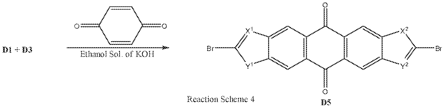
- the X 1 and Y 1 groups can be switched with the aforementioned X 2 and Y to obtain compounds D3 and D4, respectively, with D3 having a single Br group and D4 having two Br groups. Additionally, the Br? and acetic acid can be used in excess of the stoichiometric amount to synthesize compounds Dl, D2, D3, and D4. Any one of, or any combination of, Dl, D2, D3, and D4, can then be reacted with 1,4-cyclohexanedione and an ethanol solution of KOH under room temperature conditions (20 to 25 °C) and mixed until the reaction is complete (e.g., about 2 to 4 hours). In preferred embodiments, Dl and D3 can be used. The amounts of Dl , D2, D3, D4, 1,4-cyclohexanedione, and the ethanol solution of KOH can be varied as needed to produce a desired amount of the following compound D5. This is illustrated in reaction scheme 4:
- compound D6 can be prepared according to the following reaction scheme 5:
- D5 or D6 can be used in the following reaction scheraes 6 and 7, respectively, to produce compounds D7 and D8:
- the n ⁇ BuLi can be added to the R ; R * substituted acetylene compound and heated (e.g., about 60 °C) for a sufficient period of time (e.g., about 1 hour) to form a reaction mixture. Subsequently, the mixture can be cooled to room temperature and compound D5 or D6 can be added under a nitrogen stream and heated (e.g., about 60 °C) for a sufficient period of time (e.g., about 12 hours). Subsequently, the reaction mixture can be cooled to room temperature and a solution of stannyl chloride hydrate in a 10% HCl solution can be added.
- the reaction mixture can then be heated (e.g., about 60 °C) for a sufficient period of time (e.g., about 2 hours) to produce compounds D7 and D8, respectively.
- the compounds can be purified via filtration through a silica gel flask column using hexane as an eluent.
- either of compounds D7 and D8 can be further used to produce compounds D9 and D10, respectively under the following reaction scheme 8 (notably, D7 and D8 are identical to D9 and D10, respectively, when rs is 1):
- the above reaction can be performed by deprotecting and removing R 2 and R ' using tetrabutyl ammonium fluoride or CsF or KF to form alkyne functionality, followed by Cu catalyzed coupling reaction.
- the general non-limiting reaction conditions can include: 5mol% Cul or Cu(OAc)2, tri ethyl amine solvent, €b. Both steps can be peiformed separately or i one pot.
- Each of the produced electron acceptor and donor units can then be covalently linked together to form a variety of compounds (i.e., small molecules and oligomers) of the present invention.
- the covalent linkage can be made by reacting the bromine group on the electron donor unit with the trimethyitin group(s) present on the electron donor unit by using the following reaction conditions.
- a microwave glass tube can be charged with compound C (e.g., C I , C2, C3, C4, C5, or C6 or combinations thereof), compound D (e.g., Dl l ), iVii'P h ;) : and dry THF.
- the glass tube can be sealed with a Teflon® cap and stirred at room temperature following by heating the reaction mixture in a microwave to form covalent links between the electron acceptor (C) and electron donor (D) units. This is illustrated in reaction scheme 10:
- the stirring step can be for a sufficient period of time (e.g., about 15 minutes) at room temperature conditions (20 to 25 °C), and the heating step can be performed in stages (e.g., about 100 °C for 2 minutes, followed by 125 °C for 2 minutes, followed by 140 °C for 10 minutes, followed by 150 °C for 10 minutes, followed by 160 °C for 20 minutes, followed by 170 °C for 30 minutes. ).
- coordination complexes can be formed between the sulfur, selenium and tellurium atoms (i.e., M groups) on the compounds of the present invention with a coordination ligand, such as CI, Br, I, a linear, branched or cyclic aliphatic, aryl or heteroaryl group of up to 20 carbon atoms.
- a coordination ligand such as CI, Br, I, a linear, branched or cyclic aliphatic, aryl or heteroaryl group of up to 20 carbon atoms.
- FIG. 1 is a cross-sectional view of a non-limiting organic photovoltaic cell of the present invention, in which the photoactive layer is formed with the small molecules or oligomers of the present invention, or combinations thereof.
- polymers do not have to be used to form said photoactive layer.
- polymers can be used in combination with the disclosed small molecules or oligomers.
- the organic photovoltaic cell ( 1 ) can include a transparent substrate (10), a front electrode (1 1), a photoactive layer (12), and a back electrode (13). Additional materials, layers, and coatings (not shown) known to those of ordinary skill in the art can be used with photovoltaic cell (1), some of which are described below.
- the organic photovoltaic cell (1) can convert light into usable energy by: (a) photon absorption to produce excitons; (b) exciton diffusion; (c) charge transfer; and (d) charge separation and transportation to the electrodes.
- the excitons are produced by photon absorption by the photoactive layer (12), which can be a single layer such that the compounds of the present invention are the active light absorbing component in the layer.
- the preferred layer ( 12) is a bulk heteroj unction single layer.
- the substrate (10) can be used as support.
- organic photovoltaic cells it is typically transparent or translucent, which allows light to efficiently enter the cell. It is typically made from material that is not easily altered or degraded by heat or organic solvents, and as already noted, has excellent optical transparency.
- Non-limiting examples of such materials include inorganic materials such as alkali-free glass and quartz glass, polymers such as polyethylene, PET, PEN, polyimide, polyamide, polyamidoimide, polycarbonate (e.g., LexanTM, which is a polycarbonate resin offered by SABIC Innovative Plastics), liquid crystal polymer, and cycloolefin polymer, silicon, and metal.
- the front electrode (1 1 ) can be used as a cathode or anode depending on the set-up of the circuit. It is stacked on the substrate (10).
- the front electrode (1 1 ) can be made of a transparent or translucent conductive material.
- the front electrode (1 1) can be made of opaque or reflective material. Typical ly, the front electrode (1 1 ) is obtained by forming a film using such a material (e.g. , vacuum deposition, sputtering, ion-plating, plating, coating, etc.).
- transparent or translucent conductive material include metal oxide films, metal films, and conductive polymers.
- Non-limiting examples of metal oxides that can be used to form a film include indium oxide, zinc oxide, tin oxide, and their complexes such as indium stamiate (ITO), fluorine-doped tin oxide (FTO), and indium zinc oxide films.
- Non-limiting examples of metals that can be used to form a film include gold, platinum, silver, and copper.
- Non-limiting examples of conductive polymers include polyaniline and poiythiophene.
- the thickness of the film for the front electrode (1 1) is typically between from 30 to 300 nm. If the film thickness is less than 30 nm, then the conductivity can be reduced and the resi stance increased, which results in a decrease in photoelectric conversion efficiency.
- the film thickness is greater than 300 nm, then light transmittance may be lowered.
- the sheet resistance of the front electrode (11) is typical ly ⁇ ⁇ /D or less.
- the front electrode (1 1 ) may be a single layer or laminated layers formed of materials each having a different work function.
- the back electrode (13) can be used as a cathode or anode depending on the set-up of the circuit.
- Thi s electrode (13) can be made of a transparent or translucent conductive material. Alternatively, it (13) can be made of opaque or reflective material .
- This electrode (13) can be stacked on the photoactive layer (12).
- the material used for the back electrode (13) can be conductive. Non-limiting examples of such materials include metals, metal oxides, and conductive polymers (e.g., polyaniiine, polythiophene, etc.) such as those discussed above in the context of the front electrode (1 1 ).
- the front electrode (1 1) is formed using a material having high work function
- the back electrode (13) can be made of material having a low work function.
- Non-limiting examples of materials having a low work function include Li, In, Al, Ca, Mg, Sm, Tb, Yb, Zr, Na, K, Rb, Cs, Ba, and the alloys thereof
- the back electrode (13) can be a single layer or laminated layers formed of materials each having a different work function. Further, it may be an alloy of one or more of the materials having a low work function and at least one selected from the group consisting of gold, silver, platinum, copper, manganese, titanium, cobalt, nickel, tungsten, and tin.
- the alloy examples include a lithium-aluminum alloy, a lithium-magnesium alloy, a lithium-indium alloy, a magnesium-silver alloy, a magnesium-indium alloy, a magnesium- aluminum alloy, an indium-silver alloy, and a calcium-aluminum alloy.
- the film thickness of the back electrode (13) can be from 1 to 1000 nm or from 10 to 500 ran. If the film thickness is too small, then the resistance can be excessively large and the generated charge may not be sufficiently transmitted to the external circuit.
- the front (11 ) and back (13) electrodes can be further coated with hole transport or electron transport layers (not shown in FIG. 1) to increase the efficiency and prevent short circuits of the organic photovoltaic cell (1).
- the hole transport layer and the electron transport layer can be interposed between the electrode and the photoactive layer (12).
- Non-limiting examples of the materials that can be used for the hole transport layer include polythiophene-based polymers such as PEDOT/PSS (poly (3,4- ethylenedioxythiophene)-poly(styrene sulfonate)) and organic conductive polymers such as polyaniiine and polypy rrole.
- the film thickness of the hole transport layer can be from 20 to 100 nm.
- the film thickness is too low, short circuit of the electrode can occur more readily. If the film thickness is too high, the film resistance is large and the generated electric current could be limited and optical conversion efficiency can be reduced.
- the electron transport layer it can function by blocking holes and transporting electrons more efficiently.
- Non-limiting examples of the type of material that the electron transport layer can be made of include metal oxides ⁇ e.g., amorphous titanium oxide). When titanium oxide is used, the film thickness can range from 5 to 20 nm. If the film thickness is too low, the hole blocking effect can be reduced and thus the generated excitons are deactivated before the excitons dissociate into electrons and holes. By comparison, when the film thickness is too high, the film resistance is large, the generated electric current is limited, resulting in reduction of optical conversion efficiency.
- the photoactive layer (12) can be an organic or hybrid semiconducting or conducting layer.
- the layer (12) can he interposed between the front electrode (10) and the back electrode (13).
- the photoactive layer (12) can be a bulk hetero-j unction single layer such that the compounds of the present invention are the active light absorbing component in the layer.
- the layer (12) can absorb light and allow for the flow of electrons to and from the electrodes (1 1 and 13 ). Further, there can be multiple photoactive layers used for a given photovoltaic cell (e.g., 2, 3, 4, or more).
- the photoactive photoactive layer (12) on at least a portion of a surface of the electrodes (11 and 13) or on the substrate (10) or both.
- vacuum thermal evaporation which involves the heating of an organic material in vacuum and depositing said material
- organic vapor phase deposition which involves evaporation of the organic material over a substrate in the presence of an inert carrier gas
- the increased solubility of the compounds of the present invention also allows for the formation of a solution that can then be deposited onto said surfaces.
- the compounds of the present invention can be fully or partially solubilized within a solution and then deposited onto a given surface via solution-based deposition techniques (e.g., spray coating, role-to-role coating, drop casting, dip coating, Mayer rod coating, doctor blade coating, spin coating, meniscus coating, transfer printing, ink jet printing, offset printing, screen printing, gravure printing, flexo printing, dispenser coating, nozzle coating, capillar ⁇ ' coating, etc.).
- solution-based deposition techniques e.g., spray coating, role-to-role coating, drop casting, dip coating, Mayer rod coating, doctor blade coating, spin coating, meniscus coating, transfer printing, ink jet printing, offset printing, screen printing, gravure printing, flexo printing, dispenser coating, nozzle coating, capillar ⁇ ' coating, etc.
- Non-limiting examples of solvents that can be used in the context of the present invention include unsaturated hydrocarbon- based solvents (such as toluene, xylene, tetralin, decalin, mesitylene, n-butylhenzene, sec- butylbutylbenzene, and tert-butylbenzene), halogenated aromatic hydrocarbon-based solvents (such as chlorobenzene, dichiorobenzene, and trichlorobenzene), halogenated saturated hydrocarbon-based solvents (such as carbon tetrachloride, chloroform, dichloromethane, dichloroethane, chlorobutane, bromobutane, chlo opentane, chlorohexane, bromohexane, and chlorocyclohexane), ethers (such as tetrahydrofuran and tetrahydropyran), and polar aprotic solvents (such as dich
- FIGS. 2 A. and B provide two different view of thermal ellipsoid plots of compound 6.
- Compound 8 has a crystalline structure as suggested by the uniform and linear staictures viewed by scanning electron microscope (SEM) and X-ray diffraction (XRD) patterns, illustrated in FIGS. 3 and 4, respectively.
- FIG. 5 illustrates atomic force microscopy (ATM) images of films formed from compounds 8 (QuIS-S) and 10 (QuIS-Se) on a glass substrate.
- the films were cast from a solution of 5 mg/ml of compounds 8 and 10, respectively, in dichiorobenzene at 165 °C.
- FIG. 6 provides UV-Vis spectra of the compound QuIS-S and QuIS-Se films. The glass background has been subtracted and the absorbance normalized in FIG. 6. Once smooth and relatively defect-free films were prepared via the higher temperature odichlorobenzene processing to yield a solution, the thickness can be controlled, and thus electronic properties can be measured with accuracy. Tauc plots in FIG.
- FIG. 7 of the QuIS-S and QuIS-Se films illustrate the presence of direct arid indirect band gaps.
- the gaps are 1.32 eV for the indirect, and 1 .56 eV for the direct gap, whereas with QuIS-Se, the gaps are 1.26 eV for the indirect, and 1.50 eV for the direct gap.
- FIG. 8 provides ultraviolet photoelectron spectroscopy (UPS) for both films. The top two plots show the measurements from a work function scan, while the bottom two plots show the values of the valence band scan.
- FIG. 9 provides a proposed band diagram for both films, based upon the data from the Tauc plots and known values for ⁇ , PEDOT:PSS, PC71BM, and LiF/Al .
- FIG, 10 illustrates a produced bilayer OPV with a QuIS-S film and a PC71BM film.
- Table 1 provides data concerning the produced OPV:
- FIG. 1 1 provides I-V curve illustrating the best results obtained using the QuIS-S film in a bilayer configuration with a PC71 BM film .
- FIG. 12 provides an illustration of a PC7IBM and QuIS-S bulkheterojunction (BHJ) electronic device that could be prepared in the context of the present invention.
Landscapes
- Chemical & Material Sciences (AREA)
- Organic Chemistry (AREA)
- Engineering & Computer Science (AREA)
- Materials Engineering (AREA)
- Physics & Mathematics (AREA)
- Spectroscopy & Molecular Physics (AREA)
- Electromagnetism (AREA)
- Photovoltaic Devices (AREA)
- Electroluminescent Light Sources (AREA)
- Heterocyclic Carbon Compounds Containing A Hetero Ring Having Oxygen Or Sulfur (AREA)
Abstract
Description


Claims


Priority Applications (5)
| Application Number | Priority Date | Filing Date | Title |
|---|---|---|---|
| KR1020167028496A KR101732522B1 (en) | 2014-04-29 | 2015-03-25 | Synthesis of new small molecules/oligomers with high conductivity and absorption for optoelectronic application |
| EP15728930.7A EP2989108A1 (en) | 2014-04-29 | 2015-03-25 | Synthesis of new small molecules/oligomers with high conductivity and absorption for optoelectronic application |
| US14/781,872 US9444060B2 (en) | 2014-04-29 | 2015-03-25 | Synthesis of new small molecules/oligomers with high conductivity and absorption for optoelectronic application |
| JP2016549740A JP6181318B2 (en) | 2014-04-29 | 2015-03-25 | Synthesis of small molecules / oligomers with high conductivity and absorption for optoelectronic applications |
| CN201580008891.8A CN106029678A (en) | 2014-04-29 | 2015-03-25 | Synthesis of novel small molecules/oligomers with high conductivity and high absorption for optoelectronic applications |
Applications Claiming Priority (2)
| Application Number | Priority Date | Filing Date | Title |
|---|---|---|---|
| US201461985872P | 2014-04-29 | 2014-04-29 | |
| US61/985,872 | 2014-04-29 |
Publications (1)
| Publication Number | Publication Date |
|---|---|
| WO2015166360A1 true WO2015166360A1 (en) | 2015-11-05 |
Family
ID=53396521
Family Applications (1)
| Application Number | Title | Priority Date | Filing Date |
|---|---|---|---|
| PCT/IB2015/052215 Ceased WO2015166360A1 (en) | 2014-04-29 | 2015-03-25 | Synthesis of new small molecules/oligomers with high conductivity and absorption for optoelectronic application |
Country Status (6)
| Country | Link |
|---|---|
| US (1) | US9444060B2 (en) |
| EP (1) | EP2989108A1 (en) |
| JP (1) | JP6181318B2 (en) |
| KR (1) | KR101732522B1 (en) |
| CN (1) | CN106029678A (en) |
| WO (1) | WO2015166360A1 (en) |
Families Citing this family (3)
| Publication number | Priority date | Publication date | Assignee | Title |
|---|---|---|---|---|
| CN109749058B (en) * | 2017-11-02 | 2020-12-01 | 中国科学院化学研究所 | A kind of anthracene dithiophene imide polymer and its preparation method and application |
| CN108117563B (en) * | 2017-11-28 | 2019-12-03 | 华南协同创新研究院 | Anthracene bithiophene-containing organic small-molecule semiconductor material and preparation method and application thereof |
| CN110849939A (en) * | 2019-09-29 | 2020-02-28 | 深圳大学 | Doped ZnO material and preparation method thereof and acetone sensor |
Citations (2)
| Publication number | Priority date | Publication date | Assignee | Title |
|---|---|---|---|---|
| WO2012019683A2 (en) * | 2010-08-13 | 2012-02-16 | Merck Patent Gmbh | Anthra[2,3-b:7,6-b']dithiophene derivatives and their use as organic semiconductors |
| WO2012164282A1 (en) * | 2011-05-31 | 2012-12-06 | Smartkem Limited | Organic semiconductor compositions |
Family Cites Families (34)
| Publication number | Priority date | Publication date | Assignee | Title |
|---|---|---|---|---|
| US6703524B2 (en) | 2001-02-20 | 2004-03-09 | Lkt Laboratories, Inc. | Organoselenium compounds for cancer chemoprevention |
| EP1783781A3 (en) | 2003-11-28 | 2007-10-03 | Merck Patent GmbH | Organic semiconducting layer formulations comprising polyacenes and organic binder polymers |
| JP2007520602A (en) | 2004-02-04 | 2007-07-26 | ヴァロリサシオン−ルシェルシュ・リミテッド・パートナーシップ | Conductive conjugated thiophenes and their synthesis |
| US7385221B1 (en) | 2005-03-08 | 2008-06-10 | University Of Kentucky Research Foundation | Silylethynylated heteroacenes and electronic devices made therewith |
| US7309876B2 (en) | 2005-12-30 | 2007-12-18 | Lucent Technologies Inc. | Organic semiconductor having polymeric and nonpolymeric constituents |
| JP5264723B2 (en) | 2006-06-30 | 2013-08-14 | イー・アイ・デュポン・ドウ・ヌムール・アンド・カンパニー | Stabilized composition of conductive polymer and partially fluorinated acid polymer |
| KR20090033909A (en) | 2006-07-26 | 2009-04-06 | 메르크 파텐트 게엠베하 | Substituted Benzodithiophene and Benzodiselenophene |
| JP2008103464A (en) | 2006-10-18 | 2008-05-01 | Konica Minolta Holdings Inc | Organic semiconductor material, organic semiconductor film, organic semiconductor device, and organic thin film transistor |
| EP2132213B1 (en) | 2007-03-07 | 2013-05-15 | University of Kentucky Research Foundation | Silylethynylated heteroacenes and electronic devices made therewith |
| US20100117066A1 (en) | 2007-04-28 | 2010-05-13 | Merck Patent Gmbh | Organic Semiconductors |
| JP2010056476A (en) | 2008-08-29 | 2010-03-11 | Kanto Denka Kogyo Co Ltd | n-TYPE AND HETERO-JUNCTION ORGANIC THIN-FILM TRANSISTOR |
| KR20100067386A (en) | 2008-12-11 | 2010-06-21 | 엘지디스플레이 주식회사 | Organic semi-conductor low molecular and organic thin film transistor comprising the same |
| EP2404333A2 (en) | 2009-03-05 | 2012-01-11 | Konarka Technologies, Inc. | Photovoltaic cell having multiple electron donors |
| KR101084685B1 (en) | 2009-04-28 | 2011-11-17 | 한국화학연구원 | Polyacene Derivatives and Organic Thin Film Transistors Using the Same |
| US8343382B2 (en) | 2009-05-22 | 2013-01-01 | The Regents Of The University Of California | Band gap control in conjugated oligomers and polymers via Lewis acids |
| US20110031475A1 (en) | 2009-08-10 | 2011-02-10 | Xerox Corporation | Semiconductor Composition |
| KR101626363B1 (en) * | 2009-12-16 | 2016-06-02 | 엘지디스플레이 주식회사 | Anthracenyl alternating copolymer, preparation method thereof, and organic thin film transistor using the same |
| CN102668152A (en) | 2009-12-23 | 2012-09-12 | 默克专利有限公司 | Composition including polymeric binder |
| KR20120123361A (en) | 2009-12-23 | 2012-11-08 | 메르크 파텐트 게엠베하 | Compositions comprising organic semiconducting compounds |
| JP5847800B2 (en) | 2010-04-19 | 2016-01-27 | メルク パテント ゲゼルシャフト ミット ベシュレンクテル ハフツングMerck Patent Gesellschaft mit beschraenkter Haftung | Polymers of benzodithiophenes and their use as organic semiconductors |
| US8425808B2 (en) | 2010-04-27 | 2013-04-23 | Xerox Corporation | Semiconducting composition |
| IT1400116B1 (en) | 2010-05-21 | 2013-05-17 | Eni Spa | PHOTO-ACTIVE COMPOSITION WITH HIGH MOBILITY OF THE ELECTRONIC LACUNES. |
| WO2011147523A1 (en) | 2010-05-27 | 2011-12-01 | Merck Patent Gmbh | Formulation and method for preparation of organic electronic devices |
| KR20130135830A (en) | 2010-07-08 | 2013-12-11 | 메르크 파텐트 게엠베하 | Semiconducting polymers |
| EP2614068A1 (en) | 2010-09-10 | 2013-07-17 | Merck Patent GmbH | Anthra[2,3-b:7,6b']dithiophene derivatives and their use as organic semiconductors |
| RU2013122682A (en) | 2010-10-20 | 2014-11-27 | Мерк Патент Гмбх | MATCHED POLYMERS |
| RU2013130877A (en) | 2010-12-06 | 2015-01-20 | Мерк Патент Гмбх | NONLINEAR ACENE DERIVATIVES AND THEIR APPLICATION AS ORGANIC SEMICONDUCTORS |
| WO2012082893A2 (en) | 2010-12-15 | 2012-06-21 | Plextronics, Inc. | Fluoro monomers, oligomers, and polymers for inks and organic electronic devices |
| EP2699617A1 (en) | 2011-04-18 | 2014-02-26 | Merck Patent GmbH | Conjugated polymers |
| GB201108864D0 (en) | 2011-05-26 | 2011-07-06 | Ct For Process Innovation The Ltd | Transistors and methods of making them |
| TW201348241A (en) | 2011-12-30 | 2013-12-01 | Imp Innovations Ltd | Unconventional chemical doping of organic semiconducting materials |
| GB201203159D0 (en) | 2012-02-23 | 2012-04-11 | Smartkem Ltd | Organic semiconductor compositions |
| TWI635111B (en) | 2012-03-16 | 2018-09-11 | Merck Patent Gmbh | Conjugated polymer |
| US20130247989A1 (en) | 2012-03-23 | 2013-09-26 | The Regents Of The University Of California | Inert solution-processable molecular chromophores for organic electronic devices |
-
2015
- 2015-03-25 WO PCT/IB2015/052215 patent/WO2015166360A1/en not_active Ceased
- 2015-03-25 EP EP15728930.7A patent/EP2989108A1/en not_active Withdrawn
- 2015-03-25 CN CN201580008891.8A patent/CN106029678A/en active Pending
- 2015-03-25 KR KR1020167028496A patent/KR101732522B1/en not_active Expired - Fee Related
- 2015-03-25 US US14/781,872 patent/US9444060B2/en not_active Expired - Fee Related
- 2015-03-25 JP JP2016549740A patent/JP6181318B2/en not_active Expired - Fee Related
Patent Citations (2)
| Publication number | Priority date | Publication date | Assignee | Title |
|---|---|---|---|---|
| WO2012019683A2 (en) * | 2010-08-13 | 2012-02-16 | Merck Patent Gmbh | Anthra[2,3-b:7,6-b']dithiophene derivatives and their use as organic semiconductors |
| WO2012164282A1 (en) * | 2011-05-31 | 2012-12-06 | Smartkem Limited | Organic semiconductor compositions |
Also Published As
| Publication number | Publication date |
|---|---|
| KR20160132107A (en) | 2016-11-16 |
| JP6181318B2 (en) | 2017-08-16 |
| CN106029678A (en) | 2016-10-12 |
| JP2017518257A (en) | 2017-07-06 |
| KR101732522B1 (en) | 2017-05-24 |
| EP2989108A1 (en) | 2016-03-02 |
| US20160141527A1 (en) | 2016-05-19 |
| US9444060B2 (en) | 2016-09-13 |
Similar Documents
| Publication | Publication Date | Title |
|---|---|---|
| CA2860926C (en) | Synthesis of photovoltaic conjugated polymers | |
| US9246110B2 (en) | Organic material and photoelectric conversion element | |
| WO2012135527A2 (en) | Active materials for electro-optic devices and electro-optic devices | |
| US20190214581A1 (en) | Organic semiconducting compounds | |
| US9312491B2 (en) | Polymer and photoelectric conversion element | |
| US11637246B2 (en) | Organic semiconducting compounds | |
| US20170054077A1 (en) | Crystallization of additives at p/n junctions of bulk-heterojunction photoactive layers | |
| US20100084000A1 (en) | Organic photoelectric conversion device and polymer useful for producing the same | |
| US20110127515A1 (en) | Photoelectric conversion element | |
| US20210367159A1 (en) | Organic semiconducting compounds | |
| Liang et al. | Donor–acceptor conjugates-functionalized zinc phthalocyanine: Towards broad absorption and application in organic solar cells | |
| US9444060B2 (en) | Synthesis of new small molecules/oligomers with high conductivity and absorption for optoelectronic application | |
| US9543529B2 (en) | Compounds containing electron rich and electron deficient regions and their use in organic electronic applications | |
| KR101553806B1 (en) | Organic semiconductor compounds Containing Posphine oxide and Solar Cell Device Using This Material | |
| Mikroyannidis et al. | Low band-gap phenylenevinylene and fluorenevinylene small molecules containing triphenylamine segments: Synthesis and application in bulk heterojunction solar cells | |
| CN113544186A (en) | organic semiconductor composition | |
| WO2019161748A1 (en) | Organic semiconducting compounds | |
| KR101714949B1 (en) | Semiconductor polymers | |
| JP2015105233A (en) | Fullerene derivative | |
| WO2014098094A1 (en) | Organic photoelectric conversion element, organic thin-film solar cell, and composition,coating film, polymer, and compound used therein |
Legal Events
| Date | Code | Title | Description |
|---|---|---|---|
| WWE | Wipo information: entry into national phase |
Ref document number: 14781872 Country of ref document: US |
|
| WWE | Wipo information: entry into national phase |
Ref document number: 2015728930 Country of ref document: EP |
|
| 121 | Ep: the epo has been informed by wipo that ep was designated in this application |
Ref document number: 15728930 Country of ref document: EP Kind code of ref document: A1 |
|
| ENP | Entry into the national phase |
Ref document number: 2016549740 Country of ref document: JP Kind code of ref document: A |
|
| ENP | Entry into the national phase |
Ref document number: 20167028496 Country of ref document: KR Kind code of ref document: A |
|
| NENP | Non-entry into the national phase |
Ref country code: DE |