WO2012031659A1 - Anthra[2,3-b:7,6b']dithiophene derivatives and their use as organic semiconductors - Google Patents
Anthra[2,3-b:7,6b']dithiophene derivatives and their use as organic semiconductors Download PDFInfo
- Publication number
- WO2012031659A1 WO2012031659A1 PCT/EP2011/004076 EP2011004076W WO2012031659A1 WO 2012031659 A1 WO2012031659 A1 WO 2012031659A1 EP 2011004076 W EP2011004076 W EP 2011004076W WO 2012031659 A1 WO2012031659 A1 WO 2012031659A1
- Authority
- WO
- WIPO (PCT)
- Prior art keywords
- group
- groups
- atoms
- formula
- organic
- Prior art date
Links
- 239000004065 semiconductor Substances 0.000 title abstract description 35
- 238000000034 method Methods 0.000 claims abstract description 34
- -1 2,3-dimethylcyclopropyl Chemical group 0.000 claims description 185
- 150000001875 compounds Chemical class 0.000 claims description 122
- 239000010410 layer Substances 0.000 claims description 121
- 239000000203 mixture Substances 0.000 claims description 106
- 239000011230 binding agent Substances 0.000 claims description 91
- 239000000463 material Substances 0.000 claims description 61
- 238000009472 formulation Methods 0.000 claims description 55
- 239000002904 solvent Substances 0.000 claims description 54
- 239000000243 solution Substances 0.000 claims description 48
- 125000000217 alkyl group Chemical group 0.000 claims description 40
- 125000004432 carbon atom Chemical group C* 0.000 claims description 40
- 125000003118 aryl group Chemical group 0.000 claims description 26
- 239000000306 component Substances 0.000 claims description 24
- 150000002009 diols Chemical class 0.000 claims description 24
- 229920000642 polymer Polymers 0.000 claims description 24
- 239000010408 film Substances 0.000 claims description 19
- 239000000758 substrate Substances 0.000 claims description 18
- 125000001072 heteroaryl group Chemical group 0.000 claims description 17
- 229910052739 hydrogen Inorganic materials 0.000 claims description 17
- 125000001424 substituent group Chemical group 0.000 claims description 16
- 125000006413 ring segment Chemical group 0.000 claims description 15
- 125000003342 alkenyl group Chemical group 0.000 claims description 14
- 230000008569 process Effects 0.000 claims description 14
- YTPLMLYBLZKORZ-UHFFFAOYSA-N Thiophene Chemical compound C=1C=CSC=1 YTPLMLYBLZKORZ-UHFFFAOYSA-N 0.000 claims description 13
- 229910052740 iodine Inorganic materials 0.000 claims description 13
- 125000002496 methyl group Chemical group [H]C([H])([H])* 0.000 claims description 13
- AZQWKYJCGOJGHM-UHFFFAOYSA-N 1,4-benzoquinone Chemical compound O=C1C=CC(=O)C=C1 AZQWKYJCGOJGHM-UHFFFAOYSA-N 0.000 claims description 12
- MZRVEZGGRBJDDB-UHFFFAOYSA-N N-Butyllithium Chemical compound [Li]CCCC MZRVEZGGRBJDDB-UHFFFAOYSA-N 0.000 claims description 12
- 229910052731 fluorine Inorganic materials 0.000 claims description 12
- BLRPTPMANUNPDV-UHFFFAOYSA-N Silane Chemical compound [SiH4] BLRPTPMANUNPDV-UHFFFAOYSA-N 0.000 claims description 11
- 229910052744 lithium Inorganic materials 0.000 claims description 11
- 229910000077 silane Inorganic materials 0.000 claims description 11
- ZETHHMPKDUSZQQ-UHFFFAOYSA-N Betulafolienepentol Natural products C1C=C(C)CCC(C(C)CCC=C(C)C)C2C(OC)OC(OC)C2=C1 ZETHHMPKDUSZQQ-UHFFFAOYSA-N 0.000 claims description 10
- WHXSMMKQMYFTQS-UHFFFAOYSA-N Lithium Chemical compound [Li] WHXSMMKQMYFTQS-UHFFFAOYSA-N 0.000 claims description 10
- PCSMJKASWLYICJ-UHFFFAOYSA-N Succinic aldehyde Chemical compound O=CCCC=O PCSMJKASWLYICJ-UHFFFAOYSA-N 0.000 claims description 10
- 125000003545 alkoxy group Chemical group 0.000 claims description 10
- 229910052794 bromium Inorganic materials 0.000 claims description 10
- 125000004122 cyclic group Chemical group 0.000 claims description 10
- HEOKFDGOFROELJ-UHFFFAOYSA-N diacetal Natural products COc1ccc(C=C/c2cc(O)cc(OC3OC(COC(=O)c4cc(O)c(O)c(O)c4)C(O)C(O)C3O)c2)cc1O HEOKFDGOFROELJ-UHFFFAOYSA-N 0.000 claims description 10
- 125000004429 atom Chemical group 0.000 claims description 9
- LQFOPXFXVUMPTO-UHFFFAOYSA-N ethynylsilane Chemical compound [SiH3]C#[C-] LQFOPXFXVUMPTO-UHFFFAOYSA-N 0.000 claims description 9
- 230000005669 field effect Effects 0.000 claims description 9
- 239000003960 organic solvent Substances 0.000 claims description 9
- 239000002243 precursor Substances 0.000 claims description 9
- 229910008293 Li—C Inorganic materials 0.000 claims description 8
- PXHVJJICTQNCMI-UHFFFAOYSA-N Nickel Chemical compound [Ni] PXHVJJICTQNCMI-UHFFFAOYSA-N 0.000 claims description 8
- KDLHZDBZIXYQEI-UHFFFAOYSA-N Palladium Chemical compound [Pd] KDLHZDBZIXYQEI-UHFFFAOYSA-N 0.000 claims description 8
- 230000003287 optical effect Effects 0.000 claims description 8
- BWHMMNNQKKPAPP-UHFFFAOYSA-L potassium carbonate Chemical compound [K+].[K+].[O-]C([O-])=O BWHMMNNQKKPAPP-UHFFFAOYSA-L 0.000 claims description 8
- WSEJZRIZDQWMKQ-UHFFFAOYSA-N thiophene-2,3-dicarbaldehyde Chemical compound O=CC=1C=CSC=1C=O WSEJZRIZDQWMKQ-UHFFFAOYSA-N 0.000 claims description 8
- 230000002378 acidificating effect Effects 0.000 claims description 7
- 125000004448 alkyl carbonyl group Chemical group 0.000 claims description 7
- 125000000304 alkynyl group Chemical group 0.000 claims description 7
- 238000002347 injection Methods 0.000 claims description 7
- 239000007924 injection Substances 0.000 claims description 7
- 125000001997 phenyl group Chemical group [H]C1=C([H])C([H])=C(*)C([H])=C1[H] 0.000 claims description 7
- 229910052727 yttrium Inorganic materials 0.000 claims description 7
- 125000002887 hydroxy group Chemical group [H]O* 0.000 claims description 6
- 125000006850 spacer group Chemical group 0.000 claims description 6
- 125000003107 substituted aryl group Chemical group 0.000 claims description 6
- 229930192474 thiophene Natural products 0.000 claims description 6
- 239000005046 Chlorosilane Substances 0.000 claims description 5
- YLQBMQCUIZJEEH-UHFFFAOYSA-N Furan Chemical compound C=1C=COC=1 YLQBMQCUIZJEEH-UHFFFAOYSA-N 0.000 claims description 5
- 239000003990 capacitor Substances 0.000 claims description 5
- 239000003054 catalyst Substances 0.000 claims description 5
- 239000003638 chemical reducing agent Substances 0.000 claims description 5
- KOPOQZFJUQMUML-UHFFFAOYSA-N chlorosilane Chemical compound Cl[SiH3] KOPOQZFJUQMUML-UHFFFAOYSA-N 0.000 claims description 5
- 125000001495 ethyl group Chemical group [H]C([H])([H])C([H])([H])* 0.000 claims description 5
- 125000004430 oxygen atom Chemical group O* 0.000 claims description 5
- 125000004434 sulfur atom Chemical group 0.000 claims description 5
- 239000010409 thin film Substances 0.000 claims description 5
- 125000004001 thioalkyl group Chemical group 0.000 claims description 5
- FCEHBMOGCRZNNI-UHFFFAOYSA-N 1-benzothiophene Chemical compound C1=CC=C2SC=CC2=C1 FCEHBMOGCRZNNI-UHFFFAOYSA-N 0.000 claims description 4
- 229910018540 Si C Inorganic materials 0.000 claims description 4
- 125000004104 aryloxy group Chemical group 0.000 claims description 4
- IOJUPLGTWVMSFF-UHFFFAOYSA-N benzothiazole Chemical compound C1=CC=C2SC=NC2=C1 IOJUPLGTWVMSFF-UHFFFAOYSA-N 0.000 claims description 4
- 239000003153 chemical reaction reagent Substances 0.000 claims description 4
- 238000006880 cross-coupling reaction Methods 0.000 claims description 4
- 150000002148 esters Chemical class 0.000 claims description 4
- 229910052736 halogen Inorganic materials 0.000 claims description 4
- 150000002367 halogens Chemical class 0.000 claims description 4
- 125000005553 heteroaryloxy group Chemical group 0.000 claims description 4
- 230000007062 hydrolysis Effects 0.000 claims description 4
- 238000006460 hydrolysis reaction Methods 0.000 claims description 4
- 125000001449 isopropyl group Chemical group [H]C([H])([H])C([H])(*)C([H])([H])[H] 0.000 claims description 4
- 229910052749 magnesium Inorganic materials 0.000 claims description 4
- 239000011777 magnesium Substances 0.000 claims description 4
- 229910052759 nickel Inorganic materials 0.000 claims description 4
- 229910052763 palladium Inorganic materials 0.000 claims description 4
- 229910000027 potassium carbonate Inorganic materials 0.000 claims description 4
- 229910010271 silicon carbide Inorganic materials 0.000 claims description 4
- KXCAEQNNTZANTK-UHFFFAOYSA-N stannane Chemical compound [SnH4] KXCAEQNNTZANTK-UHFFFAOYSA-N 0.000 claims description 4
- 229910000080 stannane Inorganic materials 0.000 claims description 4
- HJUGFYREWKUQJT-UHFFFAOYSA-N tetrabromomethane Chemical compound BrC(Br)(Br)Br HJUGFYREWKUQJT-UHFFFAOYSA-N 0.000 claims description 4
- VZGDMQKNWNREIO-UHFFFAOYSA-N tetrachloromethane Chemical compound ClC(Cl)(Cl)Cl VZGDMQKNWNREIO-UHFFFAOYSA-N 0.000 claims description 4
- 229910052725 zinc Inorganic materials 0.000 claims description 4
- 239000011701 zinc Substances 0.000 claims description 4
- WSLDOOZREJYCGB-UHFFFAOYSA-N 1,2-Dichloroethane Chemical compound ClCCCl WSLDOOZREJYCGB-UHFFFAOYSA-N 0.000 claims description 3
- 125000003903 2-propenyl group Chemical group [H]C([*])([H])C([H])=C([H])[H] 0.000 claims description 3
- ZNZYKNKBJPZETN-WELNAUFTSA-N Dialdehyde 11678 Chemical compound N1C2=CC=CC=C2C2=C1[C@H](C[C@H](/C(=C/O)C(=O)OC)[C@@H](C=C)C=O)NCC2 ZNZYKNKBJPZETN-WELNAUFTSA-N 0.000 claims description 3
- 108091028043 Nucleic acid sequence Proteins 0.000 claims description 3
- 125000002777 acetyl group Chemical group [H]C([H])([H])C(*)=O 0.000 claims description 3
- 125000004453 alkoxycarbonyl group Chemical group 0.000 claims description 3
- 125000005194 alkoxycarbonyloxy group Chemical group 0.000 claims description 3
- 125000005196 alkyl carbonyloxy group Chemical group 0.000 claims description 3
- 125000003710 aryl alkyl group Chemical group 0.000 claims description 3
- 229910052799 carbon Inorganic materials 0.000 claims description 3
- 239000003795 chemical substances by application Substances 0.000 claims description 3
- 125000001559 cyclopropyl group Chemical group [H]C1([H])C([H])([H])C1([H])* 0.000 claims description 3
- 125000004446 heteroarylalkyl group Chemical group 0.000 claims description 3
- ARNWQMJQALNBBV-UHFFFAOYSA-N lithium carbide Chemical compound [Li+].[Li+].[C-]#[C-] ARNWQMJQALNBBV-UHFFFAOYSA-N 0.000 claims description 3
- 125000004123 n-propyl group Chemical group [H]C([H])([H])C([H])([H])C([H])([H])* 0.000 claims description 3
- 238000013086 organic photovoltaic Methods 0.000 claims description 3
- WJUKOGPNGRUXMG-UHFFFAOYSA-N 1,2-dibromo-1,1,2,2-tetrachloroethane Chemical compound ClC(Cl)(Br)C(Cl)(Cl)Br WJUKOGPNGRUXMG-UHFFFAOYSA-N 0.000 claims description 2
- PAAZPARNPHGIKF-UHFFFAOYSA-N 1,2-dibromoethane Chemical compound BrCCBr PAAZPARNPHGIKF-UHFFFAOYSA-N 0.000 claims description 2
- AIGNCQCMONAWOL-UHFFFAOYSA-N 1,3-benzoselenazole Chemical compound C1=CC=C2[se]C=NC2=C1 AIGNCQCMONAWOL-UHFFFAOYSA-N 0.000 claims description 2
- BCMCBBGGLRIHSE-UHFFFAOYSA-N 1,3-benzoxazole Chemical compound C1=CC=C2OC=NC2=C1 BCMCBBGGLRIHSE-UHFFFAOYSA-N 0.000 claims description 2
- ODIRBFFBCSTPTO-UHFFFAOYSA-N 1,3-selenazole Chemical compound C1=C[se]C=N1 ODIRBFFBCSTPTO-UHFFFAOYSA-N 0.000 claims description 2
- BNRDGHFESOHOBF-UHFFFAOYSA-N 1-benzoselenophene Chemical compound C1=CC=C2[se]C=CC2=C1 BNRDGHFESOHOBF-UHFFFAOYSA-N 0.000 claims description 2
- 125000002941 2-furyl group Chemical group O1C([*])=C([H])C([H])=C1[H] 0.000 claims description 2
- 125000000175 2-thienyl group Chemical group S1C([*])=C([H])C([H])=C1[H] 0.000 claims description 2
- 238000000018 DNA microarray Methods 0.000 claims description 2
- QZRGKCOWNLSUDK-UHFFFAOYSA-N Iodochlorine Chemical compound ICl QZRGKCOWNLSUDK-UHFFFAOYSA-N 0.000 claims description 2
- ZCQWOFVYLHDMMC-UHFFFAOYSA-N Oxazole Chemical compound C1=COC=N1 ZCQWOFVYLHDMMC-UHFFFAOYSA-N 0.000 claims description 2
- CZPWVGJYEJSRLH-UHFFFAOYSA-N Pyrimidine Chemical compound C1=CN=CN=C1 CZPWVGJYEJSRLH-UHFFFAOYSA-N 0.000 claims description 2
- FZWLAAWBMGSTSO-UHFFFAOYSA-N Thiazole Chemical compound C1=CSC=N1 FZWLAAWBMGSTSO-UHFFFAOYSA-N 0.000 claims description 2
- 125000001797 benzyl group Chemical group [H]C1=C([H])C([H])=C(C([H])=C1[H])C([H])([H])* 0.000 claims description 2
- 125000006165 cyclic alkyl group Chemical group 0.000 claims description 2
- 125000001995 cyclobutyl group Chemical group [H]C1([H])C([H])([H])C([H])(*)C1([H])[H] 0.000 claims description 2
- 125000001511 cyclopentyl group Chemical group [H]C1([H])C([H])([H])C([H])([H])C([H])(*)C1([H])[H] 0.000 claims description 2
- MROCJMGDEKINLD-UHFFFAOYSA-N dichlorosilane Chemical compound Cl[SiH2]Cl MROCJMGDEKINLD-UHFFFAOYSA-N 0.000 claims description 2
- 239000007772 electrode material Substances 0.000 claims description 2
- 125000001301 ethoxy group Chemical group [H]C([H])([H])C([H])([H])O* 0.000 claims description 2
- 150000004820 halides Chemical class 0.000 claims description 2
- 230000026030 halogenation Effects 0.000 claims description 2
- 238000005658 halogenation reaction Methods 0.000 claims description 2
- 125000005114 heteroarylalkoxy group Chemical group 0.000 claims description 2
- 239000011229 interlayer Substances 0.000 claims description 2
- PNDPGZBMCMUPRI-UHFFFAOYSA-N iodine Chemical compound II PNDPGZBMCMUPRI-UHFFFAOYSA-N 0.000 claims description 2
- 125000000555 isopropenyl group Chemical group [H]\C([H])=C(\*)C([H])([H])[H] 0.000 claims description 2
- 238000006138 lithiation reaction Methods 0.000 claims description 2
- 239000012528 membrane Substances 0.000 claims description 2
- 125000000956 methoxy group Chemical group [H]C([H])([H])O* 0.000 claims description 2
- SYSQUGFVNFXIIT-UHFFFAOYSA-N n-[4-(1,3-benzoxazol-2-yl)phenyl]-4-nitrobenzenesulfonamide Chemical class C1=CC([N+](=O)[O-])=CC=C1S(=O)(=O)NC1=CC=C(C=2OC3=CC=CC=C3N=2)C=C1 SYSQUGFVNFXIIT-UHFFFAOYSA-N 0.000 claims description 2
- PCILLCXFKWDRMK-UHFFFAOYSA-N naphthalene-1,4-diol Chemical compound C1=CC=C2C(O)=CC=C(O)C2=C1 PCILLCXFKWDRMK-UHFFFAOYSA-N 0.000 claims description 2
- WCPAKWJPBJAGKN-UHFFFAOYSA-N oxadiazole Chemical compound C1=CON=N1 WCPAKWJPBJAGKN-UHFFFAOYSA-N 0.000 claims description 2
- 125000001037 p-tolyl group Chemical group [H]C1=C([H])C(=C([H])C([H])=C1*)C([H])([H])[H] 0.000 claims description 2
- 125000000951 phenoxy group Chemical group [H]C1=C([H])C([H])=C(O*)C([H])=C1[H] 0.000 claims description 2
- 239000005518 polymer electrolyte Substances 0.000 claims description 2
- 125000002568 propynyl group Chemical group [*]C#CC([H])([H])[H] 0.000 claims description 2
- MABNMNVCOAICNO-UHFFFAOYSA-N selenophene Chemical compound C=1C=C[se]C=1 MABNMNVCOAICNO-UHFFFAOYSA-N 0.000 claims description 2
- VLLMWSRANPNYQX-UHFFFAOYSA-N thiadiazole Chemical compound C1=CSN=N1.C1=CSN=N1 VLLMWSRANPNYQX-UHFFFAOYSA-N 0.000 claims description 2
- VJYJJHQEVLEOFL-UHFFFAOYSA-N thieno[3,2-b]thiophene Chemical compound S1C=CC2=C1C=CS2 VJYJJHQEVLEOFL-UHFFFAOYSA-N 0.000 claims description 2
- 125000001462 1-pyrrolyl group Chemical group [*]N1C([H])=C([H])C([H])=C1[H] 0.000 claims 1
- 125000006169 tetracyclic group Chemical group 0.000 claims 1
- 125000006168 tricyclic group Chemical group 0.000 claims 1
- 238000002360 preparation method Methods 0.000 abstract description 3
- RTZKZFJDLAIYFH-UHFFFAOYSA-N Diethyl ether Chemical compound CCOCC RTZKZFJDLAIYFH-UHFFFAOYSA-N 0.000 description 31
- OKKJLVBELUTLKV-UHFFFAOYSA-N Methanol Chemical compound OC OKKJLVBELUTLKV-UHFFFAOYSA-N 0.000 description 30
- VYPSYNLAJGMNEJ-UHFFFAOYSA-N Silicium dioxide Chemical compound O=[Si]=O VYPSYNLAJGMNEJ-UHFFFAOYSA-N 0.000 description 28
- 230000037230 mobility Effects 0.000 description 26
- 239000007787 solid Substances 0.000 description 24
- 239000000047 product Substances 0.000 description 22
- 239000007788 liquid Substances 0.000 description 21
- 238000005160 1H NMR spectroscopy Methods 0.000 description 19
- YMWUJEATGCHHMB-UHFFFAOYSA-N Dichloromethane Chemical compound ClCCl YMWUJEATGCHHMB-UHFFFAOYSA-N 0.000 description 17
- 239000013078 crystal Substances 0.000 description 17
- 125000001570 methylene group Chemical group [H]C([H])([*:1])[*:2] 0.000 description 16
- YXFVVABEGXRONW-UHFFFAOYSA-N Toluene Chemical compound CC1=CC=CC=C1 YXFVVABEGXRONW-UHFFFAOYSA-N 0.000 description 15
- 229920001577 copolymer Chemical group 0.000 description 15
- WYURNTSHIVDZCO-UHFFFAOYSA-N Tetrahydrofuran Chemical compound C1CCOC1 WYURNTSHIVDZCO-UHFFFAOYSA-N 0.000 description 14
- 239000002800 charge carrier Substances 0.000 description 13
- 239000011541 reaction mixture Substances 0.000 description 12
- 238000001953 recrystallisation Methods 0.000 description 12
- 239000000377 silicon dioxide Substances 0.000 description 12
- CXWXQJXEFPUFDZ-UHFFFAOYSA-N tetralin Chemical compound C1=CC=C2CCCCC2=C1 CXWXQJXEFPUFDZ-UHFFFAOYSA-N 0.000 description 12
- XDTMQSROBMDMFD-UHFFFAOYSA-N Cyclohexane Chemical compound C1CCCCC1 XDTMQSROBMDMFD-UHFFFAOYSA-N 0.000 description 11
- 238000000576 coating method Methods 0.000 description 10
- 238000004519 manufacturing process Methods 0.000 description 10
- 238000002844 melting Methods 0.000 description 10
- 230000008018 melting Effects 0.000 description 10
- VLKZOEOYAKHREP-UHFFFAOYSA-N n-Hexane Chemical class CCCCCC VLKZOEOYAKHREP-UHFFFAOYSA-N 0.000 description 10
- 238000000746 purification Methods 0.000 description 10
- 239000000725 suspension Substances 0.000 description 10
- 238000003818 flash chromatography Methods 0.000 description 9
- 238000007639 printing Methods 0.000 description 9
- ZWEHNKRNPOVVGH-UHFFFAOYSA-N 2-Butanone Chemical compound CCC(C)=O ZWEHNKRNPOVVGH-UHFFFAOYSA-N 0.000 description 8
- 239000011248 coating agent Substances 0.000 description 8
- 239000002019 doping agent Substances 0.000 description 8
- 230000006870 function Effects 0.000 description 8
- 239000000178 monomer Substances 0.000 description 8
- 125000003808 silyl group Chemical group [H][Si]([H])([H])[*] 0.000 description 8
- XMWRBQBLMFGWIX-UHFFFAOYSA-N C60 fullerene Chemical compound C12=C3C(C4=C56)=C7C8=C5C5=C9C%10=C6C6=C4C1=C1C4=C6C6=C%10C%10=C9C9=C%11C5=C8C5=C8C7=C3C3=C7C2=C1C1=C2C4=C6C4=C%10C6=C9C9=C%11C5=C5C8=C3C3=C7C1=C1C2=C4C6=C2C9=C5C3=C12 XMWRBQBLMFGWIX-UHFFFAOYSA-N 0.000 description 7
- CTQNGGLPUBDAKN-UHFFFAOYSA-N O-Xylene Chemical group CC1=CC=CC=C1C CTQNGGLPUBDAKN-UHFFFAOYSA-N 0.000 description 7
- 239000003480 eluent Substances 0.000 description 7
- 239000003208 petroleum Substances 0.000 description 7
- RFFLAFLAYFXFSW-UHFFFAOYSA-N 1,2-dichlorobenzene Chemical compound ClC1=CC=CC=C1Cl RFFLAFLAYFXFSW-UHFFFAOYSA-N 0.000 description 6
- RYHBNJHYFVUHQT-UHFFFAOYSA-N 1,4-Dioxane Chemical compound C1COCCO1 RYHBNJHYFVUHQT-UHFFFAOYSA-N 0.000 description 6
- ZMXDDKWLCZADIW-UHFFFAOYSA-N N,N-Dimethylformamide Chemical compound CN(C)C=O ZMXDDKWLCZADIW-UHFFFAOYSA-N 0.000 description 6
- 230000008901 benefit Effects 0.000 description 6
- 229920001400 block copolymer Polymers 0.000 description 6
- 238000001816 cooling Methods 0.000 description 6
- 238000007641 inkjet printing Methods 0.000 description 6
- DLEDOFVPSDKWEF-UHFFFAOYSA-N lithium butane Chemical compound [Li+].CCC[CH2-] DLEDOFVPSDKWEF-UHFFFAOYSA-N 0.000 description 6
- 238000002156 mixing Methods 0.000 description 6
- 238000004528 spin coating Methods 0.000 description 6
- IVSZLXZYQVIEFR-UHFFFAOYSA-N 1,3-Dimethylbenzene Natural products CC1=CC=CC(C)=C1 IVSZLXZYQVIEFR-UHFFFAOYSA-N 0.000 description 5
- HEDRZPFGACZZDS-UHFFFAOYSA-N Chloroform Chemical compound ClC(Cl)Cl HEDRZPFGACZZDS-UHFFFAOYSA-N 0.000 description 5
- RDOXTESZEPMUJZ-UHFFFAOYSA-N anisole Chemical compound COC1=CC=CC=C1 RDOXTESZEPMUJZ-UHFFFAOYSA-N 0.000 description 5
- 238000000151 deposition Methods 0.000 description 5
- 238000005516 engineering process Methods 0.000 description 5
- 238000001704 evaporation Methods 0.000 description 5
- 229910003472 fullerene Inorganic materials 0.000 description 5
- 239000012212 insulator Substances 0.000 description 5
- 239000011347 resin Substances 0.000 description 5
- 229920005989 resin Polymers 0.000 description 5
- 238000005507 spraying Methods 0.000 description 5
- XLYOFNOQVPJJNP-UHFFFAOYSA-N water Substances O XLYOFNOQVPJJNP-UHFFFAOYSA-N 0.000 description 5
- KVNYFPKFSJIPBJ-UHFFFAOYSA-N 1,2-diethylbenzene Chemical compound CCC1=CC=CC=C1CC KVNYFPKFSJIPBJ-UHFFFAOYSA-N 0.000 description 4
- URLKBWYHVLBVBO-UHFFFAOYSA-N Para-Xylene Chemical group CC1=CC=C(C)C=C1 URLKBWYHVLBVBO-UHFFFAOYSA-N 0.000 description 4
- 239000004793 Polystyrene Substances 0.000 description 4
- PPBRXRYQALVLMV-UHFFFAOYSA-N Styrene Chemical compound C=CC1=CC=CC=C1 PPBRXRYQALVLMV-UHFFFAOYSA-N 0.000 description 4
- 150000004982 aromatic amines Chemical class 0.000 description 4
- 230000015572 biosynthetic process Effects 0.000 description 4
- NNBZCPXTIHJBJL-UHFFFAOYSA-N decalin Chemical compound C1CCCC2CCCCC21 NNBZCPXTIHJBJL-UHFFFAOYSA-N 0.000 description 4
- 230000008020 evaporation Effects 0.000 description 4
- 238000001914 filtration Methods 0.000 description 4
- 239000001257 hydrogen Substances 0.000 description 4
- 229910052751 metal Inorganic materials 0.000 description 4
- 239000002184 metal Substances 0.000 description 4
- 229920002223 polystyrene Polymers 0.000 description 4
- 239000002244 precipitate Substances 0.000 description 4
- 229910052701 rubidium Inorganic materials 0.000 description 4
- 239000000741 silica gel Substances 0.000 description 4
- 229910002027 silica gel Inorganic materials 0.000 description 4
- 125000000547 substituted alkyl group Chemical group 0.000 description 4
- 229920002554 vinyl polymer Polymers 0.000 description 4
- OISVCGZHLKNMSJ-UHFFFAOYSA-N 2,6-dimethylpyridine Chemical compound CC1=CC=CC(C)=N1 OISVCGZHLKNMSJ-UHFFFAOYSA-N 0.000 description 3
- 229920003026 Acene Polymers 0.000 description 3
- XEKOWRVHYACXOJ-UHFFFAOYSA-N Ethyl acetate Chemical compound CCOC(C)=O XEKOWRVHYACXOJ-UHFFFAOYSA-N 0.000 description 3
- 150000001555 benzenes Chemical class 0.000 description 3
- JFDZBHWFFUWGJE-UHFFFAOYSA-N benzonitrile Chemical compound N#CC1=CC=CC=C1 JFDZBHWFFUWGJE-UHFFFAOYSA-N 0.000 description 3
- 238000009835 boiling Methods 0.000 description 3
- MVPPADPHJFYWMZ-UHFFFAOYSA-N chlorobenzene Chemical compound ClC1=CC=CC=C1 MVPPADPHJFYWMZ-UHFFFAOYSA-N 0.000 description 3
- 229960001701 chloroform Drugs 0.000 description 3
- 238000004440 column chromatography Methods 0.000 description 3
- 239000012043 crude product Substances 0.000 description 3
- 239000003085 diluting agent Substances 0.000 description 3
- 238000003618 dip coating Methods 0.000 description 3
- 239000000706 filtrate Substances 0.000 description 3
- RMBPEFMHABBEKP-UHFFFAOYSA-N fluorene Chemical compound C1=CC=C2C3=C[CH]C=CC3=CC2=C1 RMBPEFMHABBEKP-UHFFFAOYSA-N 0.000 description 3
- 229920002313 fluoropolymer Polymers 0.000 description 3
- 239000004811 fluoropolymer Substances 0.000 description 3
- 239000010931 gold Substances 0.000 description 3
- 238000011065 in-situ storage Methods 0.000 description 3
- NIHNNTQXNPWCJQ-UHFFFAOYSA-N o-biphenylenemethane Natural products C1=CC=C2CC3=CC=CC=C3C2=C1 NIHNNTQXNPWCJQ-UHFFFAOYSA-N 0.000 description 3
- 239000012044 organic layer Substances 0.000 description 3
- 229910052705 radium Inorganic materials 0.000 description 3
- 125000002914 sec-butyl group Chemical group [H]C([H])([H])C([H])([H])C([H])(*)C([H])([H])[H] 0.000 description 3
- 239000011877 solvent mixture Substances 0.000 description 3
- 239000000126 substance Substances 0.000 description 3
- 229910052717 sulfur Inorganic materials 0.000 description 3
- 238000003786 synthesis reaction Methods 0.000 description 3
- 239000008096 xylene Substances 0.000 description 3
- GETTZEONDQJALK-UHFFFAOYSA-N (trifluoromethyl)benzene Chemical compound FC(F)(F)C1=CC=CC=C1 GETTZEONDQJALK-UHFFFAOYSA-N 0.000 description 2
- QPFMBZIOSGYJDE-UHFFFAOYSA-N 1,1,2,2-tetrachloroethane Chemical compound ClC(Cl)C(Cl)Cl QPFMBZIOSGYJDE-UHFFFAOYSA-N 0.000 description 2
- BFIMMTCNYPIMRN-UHFFFAOYSA-N 1,2,3,5-tetramethylbenzene Chemical compound CC1=CC(C)=C(C)C(C)=C1 BFIMMTCNYPIMRN-UHFFFAOYSA-N 0.000 description 2
- GWHJZXXIDMPWGX-UHFFFAOYSA-N 1,2,4-trimethylbenzene Chemical compound CC1=CC=C(C)C(C)=C1 GWHJZXXIDMPWGX-UHFFFAOYSA-N 0.000 description 2
- VZHJIJZEOCBKRA-UHFFFAOYSA-N 1-chloro-3-fluorobenzene Chemical compound FC1=CC=CC(Cl)=C1 VZHJIJZEOCBKRA-UHFFFAOYSA-N 0.000 description 2
- QPUYECUOLPXSFR-UHFFFAOYSA-N 1-methylnaphthalene Chemical compound C1=CC=C2C(C)=CC=CC2=C1 QPUYECUOLPXSFR-UHFFFAOYSA-N 0.000 description 2
- OHZAHWOAMVVGEL-UHFFFAOYSA-N 2,2'-bithiophene Chemical group C1=CSC(C=2SC=CC=2)=C1 OHZAHWOAMVVGEL-UHFFFAOYSA-N 0.000 description 2
- OXQOBQJCDNLAPO-UHFFFAOYSA-N 2,3-Dimethylpyrazine Chemical compound CC1=NC=CN=C1C OXQOBQJCDNLAPO-UHFFFAOYSA-N 0.000 description 2
- 125000004493 2-methylbut-1-yl group Chemical group CC(C*)CC 0.000 description 2
- 125000004975 3-butenyl group Chemical group C(CC=C)* 0.000 description 2
- UJOBWOGCFQCDNV-UHFFFAOYSA-N 9H-carbazole Chemical group C1=CC=C2C3=CC=CC=C3NC2=C1 UJOBWOGCFQCDNV-UHFFFAOYSA-N 0.000 description 2
- CSCPPACGZOOCGX-UHFFFAOYSA-N Acetone Chemical compound CC(C)=O CSCPPACGZOOCGX-UHFFFAOYSA-N 0.000 description 2
- KAKZBPTYRLMSJV-UHFFFAOYSA-N Butadiene Chemical compound C=CC=C KAKZBPTYRLMSJV-UHFFFAOYSA-N 0.000 description 2
- 0 CN(C(C(N)=C1N=C*)=O)C1=O Chemical compound CN(C(C(N)=C1N=C*)=O)C1=O 0.000 description 2
- IAZDPXIOMUYVGZ-UHFFFAOYSA-N Dimethylsulphoxide Chemical compound CS(C)=O IAZDPXIOMUYVGZ-UHFFFAOYSA-N 0.000 description 2
- 208000033962 Fontaine progeroid syndrome Diseases 0.000 description 2
- 239000004890 Hydrophobing Agent Substances 0.000 description 2
- CSNNHWWHGAXBCP-UHFFFAOYSA-L Magnesium sulfate Chemical compound [Mg+2].[O-][S+2]([O-])([O-])[O-] CSNNHWWHGAXBCP-UHFFFAOYSA-L 0.000 description 2
- YNAVUWVOSKDBBP-UHFFFAOYSA-N Morpholine Chemical compound C1COCCN1 YNAVUWVOSKDBBP-UHFFFAOYSA-N 0.000 description 2
- SECXISVLQFMRJM-UHFFFAOYSA-N N-Methylpyrrolidone Chemical compound CN1CCCC1=O SECXISVLQFMRJM-UHFFFAOYSA-N 0.000 description 2
- PWATWSYOIIXYMA-UHFFFAOYSA-N Pentylbenzene Chemical compound CCCCCC1=CC=CC=C1 PWATWSYOIIXYMA-UHFFFAOYSA-N 0.000 description 2
- 239000005062 Polybutadiene Substances 0.000 description 2
- JUJWROOIHBZHMG-UHFFFAOYSA-N Pyridine Chemical compound C1=CC=NC=C1 JUJWROOIHBZHMG-UHFFFAOYSA-N 0.000 description 2
- MOYAFQVGZZPNRA-UHFFFAOYSA-N Terpinolene Chemical compound CC(C)=C1CCC(C)=CC1 MOYAFQVGZZPNRA-UHFFFAOYSA-N 0.000 description 2
- XLOMVQKBTHCTTD-UHFFFAOYSA-N Zinc monoxide Chemical compound [Zn]=O XLOMVQKBTHCTTD-UHFFFAOYSA-N 0.000 description 2
- MCEWYIDBDVPMES-UHFFFAOYSA-N [60]pcbm Chemical compound C123C(C4=C5C6=C7C8=C9C%10=C%11C%12=C%13C%14=C%15C%16=C%17C%18=C(C=%19C=%20C%18=C%18C%16=C%13C%13=C%11C9=C9C7=C(C=%20C9=C%13%18)C(C7=%19)=C96)C6=C%11C%17=C%15C%13=C%15C%14=C%12C%12=C%10C%10=C85)=C9C7=C6C2=C%11C%13=C2C%15=C%12C%10=C4C23C1(CCCC(=O)OC)C1=CC=CC=C1 MCEWYIDBDVPMES-UHFFFAOYSA-N 0.000 description 2
- 239000000853 adhesive Substances 0.000 description 2
- 239000003570 air Substances 0.000 description 2
- HSFWRNGVRCDJHI-UHFFFAOYSA-N alpha-acetylene Natural products C#C HSFWRNGVRCDJHI-UHFFFAOYSA-N 0.000 description 2
- 150000001450 anions Chemical class 0.000 description 2
- 238000000137 annealing Methods 0.000 description 2
- 239000002518 antifoaming agent Substances 0.000 description 2
- 239000012298 atmosphere Substances 0.000 description 2
- ILAHWRKJUDSMFH-UHFFFAOYSA-N boron tribromide Chemical compound BrB(Br)Br ILAHWRKJUDSMFH-UHFFFAOYSA-N 0.000 description 2
- CASOXAYOCHCWQU-UHFFFAOYSA-N butan-2-one;ethanol Chemical compound CCO.CCC(C)=O CASOXAYOCHCWQU-UHFFFAOYSA-N 0.000 description 2
- NOCUHXPGWAPFGO-UHFFFAOYSA-N butan-2-one;propan-2-ol Chemical compound CC(C)O.CCC(C)=O NOCUHXPGWAPFGO-UHFFFAOYSA-N 0.000 description 2
- DKPFZGUDAPQIHT-UHFFFAOYSA-N butyl acetate Chemical compound CCCCOC(C)=O DKPFZGUDAPQIHT-UHFFFAOYSA-N 0.000 description 2
- 125000000484 butyl group Chemical group [H]C([*])([H])C([H])([H])C([H])([H])C([H])([H])[H] 0.000 description 2
- 239000000969 carrier Substances 0.000 description 2
- 238000012512 characterization method Methods 0.000 description 2
- 238000006243 chemical reaction Methods 0.000 description 2
- 239000002322 conducting polymer Substances 0.000 description 2
- 229920001940 conductive polymer Polymers 0.000 description 2
- RWGFKTVRMDUZSP-UHFFFAOYSA-N cumene Chemical compound CC(C)C1=CC=CC=C1 RWGFKTVRMDUZSP-UHFFFAOYSA-N 0.000 description 2
- JHIVVAPYMSGYDF-UHFFFAOYSA-N cyclohexanone Chemical compound O=C1CCCCC1 JHIVVAPYMSGYDF-UHFFFAOYSA-N 0.000 description 2
- 229930007927 cymene Natural products 0.000 description 2
- 230000007547 defect Effects 0.000 description 2
- 238000010511 deprotection reaction Methods 0.000 description 2
- 230000001627 detrimental effect Effects 0.000 description 2
- GSENNYNYEKCQGA-UHFFFAOYSA-N dichloro-di(propan-2-yl)silane Chemical compound CC(C)[Si](Cl)(Cl)C(C)C GSENNYNYEKCQGA-UHFFFAOYSA-N 0.000 description 2
- 239000003989 dielectric material Substances 0.000 description 2
- 238000010790 dilution Methods 0.000 description 2
- 239000012895 dilution Substances 0.000 description 2
- ZUOUZKKEUPVFJK-UHFFFAOYSA-N diphenyl Chemical compound C1=CC=CC=C1C1=CC=CC=C1 ZUOUZKKEUPVFJK-UHFFFAOYSA-N 0.000 description 2
- 238000007598 dipping method Methods 0.000 description 2
- 239000002270 dispersing agent Substances 0.000 description 2
- 239000000975 dye Substances 0.000 description 2
- 230000000694 effects Effects 0.000 description 2
- 125000005678 ethenylene group Chemical group [H]C([*:1])=C([H])[*:2] 0.000 description 2
- MTZQAGJQAFMTAQ-UHFFFAOYSA-N ethyl benzoate Chemical compound CCOC(=O)C1=CC=CC=C1 MTZQAGJQAFMTAQ-UHFFFAOYSA-N 0.000 description 2
- 125000002534 ethynyl group Chemical group [H]C#C* 0.000 description 2
- 239000012530 fluid Substances 0.000 description 2
- 238000004508 fractional distillation Methods 0.000 description 2
- 238000002290 gas chromatography-mass spectrometry Methods 0.000 description 2
- 238000007429 general method Methods 0.000 description 2
- PQNFLJBBNBOBRQ-UHFFFAOYSA-N indane Chemical compound C1=CC=C2CCCC2=C1 PQNFLJBBNBOBRQ-UHFFFAOYSA-N 0.000 description 2
- 239000003112 inhibitor Substances 0.000 description 2
- 125000001972 isopentyl group Chemical group [H]C([H])([H])C([H])(C([H])([H])[H])C([H])([H])C([H])([H])* 0.000 description 2
- XMGQYMWWDOXHJM-UHFFFAOYSA-N limonene Chemical compound CC(=C)C1CCC(C)=CC1 XMGQYMWWDOXHJM-UHFFFAOYSA-N 0.000 description 2
- 239000004973 liquid crystal related substance Substances 0.000 description 2
- WDDOQHLJFOUQMW-UHFFFAOYSA-N lithium;ethynyl(trimethyl)silane Chemical compound [Li+].C[Si](C)(C)C#[C-] WDDOQHLJFOUQMW-UHFFFAOYSA-N 0.000 description 2
- 239000000314 lubricant Substances 0.000 description 2
- 229910052943 magnesium sulfate Inorganic materials 0.000 description 2
- DQEUYIQDSMINEY-UHFFFAOYSA-M magnesium;prop-1-ene;bromide Chemical compound [Mg+2].[Br-].[CH2-]C=C DQEUYIQDSMINEY-UHFFFAOYSA-M 0.000 description 2
- UZKWTJUDCOPSNM-UHFFFAOYSA-N methoxybenzene Substances CCCCOC=C UZKWTJUDCOPSNM-UHFFFAOYSA-N 0.000 description 2
- 239000012299 nitrogen atmosphere Substances 0.000 description 2
- 229940078552 o-xylene Drugs 0.000 description 2
- 239000003921 oil Substances 0.000 description 2
- 125000001181 organosilyl group Chemical group [SiH3]* 0.000 description 2
- 229910052760 oxygen Inorganic materials 0.000 description 2
- HFPZCAJZSCWRBC-UHFFFAOYSA-N p-cymene Chemical compound CC(C)C1=CC=C(C)C=C1 HFPZCAJZSCWRBC-UHFFFAOYSA-N 0.000 description 2
- 238000012856 packing Methods 0.000 description 2
- 238000010422 painting Methods 0.000 description 2
- SLIUAWYAILUBJU-UHFFFAOYSA-N pentacene Chemical compound C1=CC=CC2=CC3=CC4=CC5=CC=CC=C5C=C4C=C3C=C21 SLIUAWYAILUBJU-UHFFFAOYSA-N 0.000 description 2
- 150000002964 pentacenes Chemical class 0.000 description 2
- 239000012071 phase Substances 0.000 description 2
- 125000000843 phenylene group Chemical group C1(=C(C=CC=C1)*)* 0.000 description 2
- 239000000049 pigment Substances 0.000 description 2
- 229920000314 poly p-methyl styrene Polymers 0.000 description 2
- 229920003227 poly(N-vinyl carbazole) Polymers 0.000 description 2
- 229920002857 polybutadiene Polymers 0.000 description 2
- UOHMMEJUHBCKEE-UHFFFAOYSA-N prehnitene Chemical compound CC1=CC=C(C)C(C)=C1C UOHMMEJUHBCKEE-UHFFFAOYSA-N 0.000 description 2
- 238000012545 processing Methods 0.000 description 2
- 125000001436 propyl group Chemical group [H]C([*])([H])C([H])([H])C([H])([H])[H] 0.000 description 2
- 125000006239 protecting group Chemical group 0.000 description 2
- 150000003254 radicals Chemical class 0.000 description 2
- 230000009467 reduction Effects 0.000 description 2
- 238000010020 roller printing Methods 0.000 description 2
- 229910052711 selenium Inorganic materials 0.000 description 2
- 229910052710 silicon Inorganic materials 0.000 description 2
- 239000003381 stabilizer Substances 0.000 description 2
- 238000003756 stirring Methods 0.000 description 2
- 238000001308 synthesis method Methods 0.000 description 2
- RTYNRTUKJVYEIE-UHFFFAOYSA-N tert-butyl-ethynyl-dimethylsilane Chemical group CC(C)(C)[Si](C)(C)C#C RTYNRTUKJVYEIE-UHFFFAOYSA-N 0.000 description 2
- 125000004665 trialkylsilyl group Chemical group 0.000 description 2
- 125000005259 triarylamine group Chemical group 0.000 description 2
- PXXNTAGJWPJAGM-UHFFFAOYSA-N vertaline Natural products C1C2C=3C=C(OC)C(OC)=CC=3OC(C=C3)=CC=C3CCC(=O)OC1CC1N2CCCC1 PXXNTAGJWPJAGM-UHFFFAOYSA-N 0.000 description 2
- 125000000391 vinyl group Chemical group [H]C([*])=C([H])[H] 0.000 description 2
- 239000000080 wetting agent Substances 0.000 description 2
- ICPSWZFVWAPUKF-UHFFFAOYSA-N 1,1'-spirobi[fluorene] Chemical compound C1=CC=C2C=C3C4(C=5C(C6=CC=CC=C6C=5)=CC=C4)C=CC=C3C2=C1 ICPSWZFVWAPUKF-UHFFFAOYSA-N 0.000 description 1
- BULLJMKUVKYZDJ-UHFFFAOYSA-N 1,1,1,2,2,3,3,4,4,5,5,6,6-tridecafluoro-6-iodohexane Chemical compound FC(F)(F)C(F)(F)C(F)(F)C(F)(F)C(F)(F)C(F)(F)I BULLJMKUVKYZDJ-UHFFFAOYSA-N 0.000 description 1
- UOCLXMDMGBRAIB-UHFFFAOYSA-N 1,1,1-trichloroethane Chemical compound CC(Cl)(Cl)Cl UOCLXMDMGBRAIB-UHFFFAOYSA-N 0.000 description 1
- YSNVKDGEALPJGC-UHFFFAOYSA-N 1,4-difluoro-2-methylbenzene Chemical compound CC1=CC(F)=CC=C1F YSNVKDGEALPJGC-UHFFFAOYSA-N 0.000 description 1
- 125000001140 1,4-phenylene group Chemical group [H]C1=C([H])C([*:2])=C([H])C([H])=C1[*:1] 0.000 description 1
- OSIGJGFTADMDOB-UHFFFAOYSA-N 1-Methoxy-3-methylbenzene Chemical compound COC1=CC=CC(C)=C1 OSIGJGFTADMDOB-UHFFFAOYSA-N 0.000 description 1
- AJCSNHQKXUSMMY-UHFFFAOYSA-N 1-chloro-2,4-difluorobenzene Chemical compound FC1=CC=C(Cl)C(F)=C1 AJCSNHQKXUSMMY-UHFFFAOYSA-N 0.000 description 1
- DGRVQOKCSKDWIH-UHFFFAOYSA-N 1-chloro-2-(trifluoromethyl)benzene Chemical compound FC(F)(F)C1=CC=CC=C1Cl DGRVQOKCSKDWIH-UHFFFAOYSA-N 0.000 description 1
- ZCJAYDKWZAWMPR-UHFFFAOYSA-N 1-chloro-2-fluorobenzene Chemical compound FC1=CC=CC=C1Cl ZCJAYDKWZAWMPR-UHFFFAOYSA-N 0.000 description 1
- FNPVYRJTBXHIPB-UHFFFAOYSA-N 1-chloro-3-fluoro-2-methylbenzene Chemical compound CC1=C(F)C=CC=C1Cl FNPVYRJTBXHIPB-UHFFFAOYSA-N 0.000 description 1
- RJCGZNCCVKIBHO-UHFFFAOYSA-N 1-chloro-4-fluorobenzene Chemical compound FC1=CC=C(Cl)C=C1 RJCGZNCCVKIBHO-UHFFFAOYSA-N 0.000 description 1
- AWLDSXJCQWTJPC-UHFFFAOYSA-N 1-fluoro-2,3-dimethylbenzene Chemical group CC1=CC=CC(F)=C1C AWLDSXJCQWTJPC-UHFFFAOYSA-N 0.000 description 1
- BGVGHYOIWIALFF-UHFFFAOYSA-N 1-fluoro-2-(trifluoromethyl)benzene Chemical compound FC1=CC=CC=C1C(F)(F)F BGVGHYOIWIALFF-UHFFFAOYSA-N 0.000 description 1
- JIXDOBAQOWOUPA-UHFFFAOYSA-N 1-fluoro-2-methoxybenzene Chemical compound COC1=CC=CC=C1F JIXDOBAQOWOUPA-UHFFFAOYSA-N 0.000 description 1
- MMZYCBHLNZVROM-UHFFFAOYSA-N 1-fluoro-2-methylbenzene Chemical compound CC1=CC=CC=C1F MMZYCBHLNZVROM-UHFFFAOYSA-N 0.000 description 1
- IWFKMNAEFPEIOY-UHFFFAOYSA-N 1-fluoro-3,5-dimethoxybenzene Chemical compound COC1=CC(F)=CC(OC)=C1 IWFKMNAEFPEIOY-UHFFFAOYSA-N 0.000 description 1
- GBOWGKOVMBDPJF-UHFFFAOYSA-N 1-fluoro-3-(trifluoromethyl)benzene Chemical compound FC1=CC=CC(C(F)(F)F)=C1 GBOWGKOVMBDPJF-UHFFFAOYSA-N 0.000 description 1
- MFJNOXOAIFNSBX-UHFFFAOYSA-N 1-fluoro-3-methoxybenzene Chemical compound COC1=CC=CC(F)=C1 MFJNOXOAIFNSBX-UHFFFAOYSA-N 0.000 description 1
- BTQZKHUEUDPRST-UHFFFAOYSA-N 1-fluoro-3-methylbenzene Chemical compound CC1=CC=CC(F)=C1 BTQZKHUEUDPRST-UHFFFAOYSA-N 0.000 description 1
- UNNNAIWPDLRVRN-UHFFFAOYSA-N 1-fluoro-4-(trifluoromethyl)benzene Chemical compound FC1=CC=C(C(F)(F)F)C=C1 UNNNAIWPDLRVRN-UHFFFAOYSA-N 0.000 description 1
- VIPWUFMFHBIKQI-UHFFFAOYSA-N 1-fluoro-4-methoxybenzene Chemical compound COC1=CC=C(F)C=C1 VIPWUFMFHBIKQI-UHFFFAOYSA-N 0.000 description 1
- WRWPPGUCZBJXKX-UHFFFAOYSA-N 1-fluoro-4-methylbenzene Chemical compound CC1=CC=C(F)C=C1 WRWPPGUCZBJXKX-UHFFFAOYSA-N 0.000 description 1
- JCHJBEZBHANKGA-UHFFFAOYSA-N 1-methoxy-3,5-dimethylbenzene Chemical compound COC1=CC(C)=CC(C)=C1 JCHJBEZBHANKGA-UHFFFAOYSA-N 0.000 description 1
- XHONYVFDZSPELQ-UHFFFAOYSA-N 1-methoxy-3-(trifluoromethyl)benzene Chemical compound COC1=CC=CC(C(F)(F)F)=C1 XHONYVFDZSPELQ-UHFFFAOYSA-N 0.000 description 1
- KWSHGRJUSUJPQD-UHFFFAOYSA-N 1-phenyl-4-propan-2-ylbenzene Chemical group C1=CC(C(C)C)=CC=C1C1=CC=CC=C1 KWSHGRJUSUJPQD-UHFFFAOYSA-N 0.000 description 1
- QCWXDVFBZVHKLV-UHFFFAOYSA-N 1-tert-butyl-4-methylbenzene Chemical compound CC1=CC=C(C(C)(C)C)C=C1 QCWXDVFBZVHKLV-UHFFFAOYSA-N 0.000 description 1
- 238000001644 13C nuclear magnetic resonance spectroscopy Methods 0.000 description 1
- KAESVJOAVNADME-UHFFFAOYSA-N 1H-pyrrole Natural products C=1C=CNC=1 KAESVJOAVNADME-UHFFFAOYSA-N 0.000 description 1
- PDQRQJVPEFGVRK-UHFFFAOYSA-N 2,1,3-benzothiadiazole Chemical compound C1=CC=CC2=NSN=C21 PDQRQJVPEFGVRK-UHFFFAOYSA-N 0.000 description 1
- UJCFZCTTZWHRNL-UHFFFAOYSA-N 2,4-Dimethylanisole Chemical compound COC1=CC=C(C)C=C1C UJCFZCTTZWHRNL-UHFFFAOYSA-N 0.000 description 1
- XWCKSJOUZQHFKI-UHFFFAOYSA-N 2-chloro-1,4-difluorobenzene Chemical compound FC1=CC=C(F)C(Cl)=C1 XWCKSJOUZQHFKI-UHFFFAOYSA-N 0.000 description 1
- QJQZRLXDLORINA-UHFFFAOYSA-N 2-cyclohexylethanol Chemical compound OCCC1CCCCC1 QJQZRLXDLORINA-UHFFFAOYSA-N 0.000 description 1
- GDHXJNRAJRCGMX-UHFFFAOYSA-N 2-fluorobenzonitrile Chemical compound FC1=CC=CC=C1C#N GDHXJNRAJRCGMX-UHFFFAOYSA-N 0.000 description 1
- MTAODLNXWYIKSO-UHFFFAOYSA-N 2-fluoropyridine Chemical compound FC1=CC=CC=N1 MTAODLNXWYIKSO-UHFFFAOYSA-N 0.000 description 1
- GFNZJAUVJCGWLW-UHFFFAOYSA-N 2-methoxy-1,3-dimethylbenzene Chemical compound COC1=C(C)C=CC=C1C GFNZJAUVJCGWLW-UHFFFAOYSA-N 0.000 description 1
- SJZAUIVYZWPNAS-UHFFFAOYSA-N 2-methoxy-1,4-dimethylbenzene Chemical compound COC1=CC(C)=CC=C1C SJZAUIVYZWPNAS-UHFFFAOYSA-N 0.000 description 1
- 125000004200 2-methoxyethyl group Chemical group [H]C([H])([H])OC([H])([H])C([H])([H])* 0.000 description 1
- XWKFPIODWVPXLX-UHFFFAOYSA-N 2-methyl-5-methylpyridine Natural products CC1=CC=C(C)N=C1 XWKFPIODWVPXLX-UHFFFAOYSA-N 0.000 description 1
- DTFKRVXLBCAIOZ-UHFFFAOYSA-N 2-methylanisole Chemical compound COC1=CC=CC=C1C DTFKRVXLBCAIOZ-UHFFFAOYSA-N 0.000 description 1
- 125000005916 2-methylpentyl group Chemical group 0.000 description 1
- BXVVMSMTWXVEOH-UHFFFAOYSA-N 3,6-bis(difluoromethylidene)cyclohexa-1,4-diene Chemical group FC(F)=C1C=CC(=C(F)F)C=C1 BXVVMSMTWXVEOH-UHFFFAOYSA-N 0.000 description 1
- JZTPKAROPNTQQV-UHFFFAOYSA-N 3-fluorobenzonitrile Chemical compound FC1=CC=CC(C#N)=C1 JZTPKAROPNTQQV-UHFFFAOYSA-N 0.000 description 1
- CELKOWQJPVJKIL-UHFFFAOYSA-N 3-fluoropyridine Chemical compound FC1=CC=CN=C1 CELKOWQJPVJKIL-UHFFFAOYSA-N 0.000 description 1
- MCSXGCZMEPXKIW-UHFFFAOYSA-N 3-hydroxy-4-[(4-methyl-2-nitrophenyl)diazenyl]-N-(3-nitrophenyl)naphthalene-2-carboxamide Chemical compound Cc1ccc(N=Nc2c(O)c(cc3ccccc23)C(=O)Nc2cccc(c2)[N+]([O-])=O)c(c1)[N+]([O-])=O MCSXGCZMEPXKIW-UHFFFAOYSA-N 0.000 description 1
- 125000001331 3-methylbutoxy group Chemical group [H]C([H])([H])C([H])(C([H])([H])[H])C([H])([H])C([H])([H])O* 0.000 description 1
- 125000005917 3-methylpentyl group Chemical group 0.000 description 1
- XMIIGOLPHOKFCH-UHFFFAOYSA-N 3-phenylpropionic acid Chemical compound OC(=O)CCC1=CC=CC=C1 XMIIGOLPHOKFCH-UHFFFAOYSA-N 0.000 description 1
- DAGKHJDZYJFWSO-UHFFFAOYSA-N 4-fluoro-1,2-dimethoxybenzene Chemical compound COC1=CC=C(F)C=C1OC DAGKHJDZYJFWSO-UHFFFAOYSA-N 0.000 description 1
- 125000006043 5-hexenyl group Chemical group 0.000 description 1
- ZCYVEMRRCGMTRW-UHFFFAOYSA-N 7553-56-2 Chemical compound [I] ZCYVEMRRCGMTRW-UHFFFAOYSA-N 0.000 description 1
- 229910021630 Antimony pentafluoride Inorganic materials 0.000 description 1
- 241000913992 Aprion Species 0.000 description 1
- 229910017049 AsF5 Inorganic materials 0.000 description 1
- 229910015845 BBr3 Inorganic materials 0.000 description 1
- 229910015900 BF3 Inorganic materials 0.000 description 1
- ZFJNIEBVYIYDEH-UHFFFAOYSA-N CC(C)(C)[Si](C)(C)C#Cc(c1c2cc3[s]c(F)cc3c1)c(cc1[s]c(F)cc1c1)c1c2C#C[Si+](C)(C)C(C)(C)C Chemical compound CC(C)(C)[Si](C)(C)C#Cc(c1c2cc3[s]c(F)cc3c1)c(cc1[s]c(F)cc1c1)c1c2C#C[Si+](C)(C)C(C)(C)C ZFJNIEBVYIYDEH-UHFFFAOYSA-N 0.000 description 1
- BVKZGUZCCUSVTD-UHFFFAOYSA-L Carbonate Chemical compound [O-]C([O-])=O BVKZGUZCCUSVTD-UHFFFAOYSA-L 0.000 description 1
- VEXZGXHMUGYJMC-UHFFFAOYSA-M Chloride anion Chemical compound [Cl-] VEXZGXHMUGYJMC-UHFFFAOYSA-M 0.000 description 1
- SNRUBQQJIBEYMU-UHFFFAOYSA-N Dodecane Natural products CCCCCCCCCCCC SNRUBQQJIBEYMU-UHFFFAOYSA-N 0.000 description 1
- 239000004593 Epoxy Substances 0.000 description 1
- 239000005977 Ethylene Substances 0.000 description 1
- 206010073306 Exposure to radiation Diseases 0.000 description 1
- 229910005185 FSO3H Inorganic materials 0.000 description 1
- PXGOKWXKJXAPGV-UHFFFAOYSA-N Fluorine Chemical compound FF PXGOKWXKJXAPGV-UHFFFAOYSA-N 0.000 description 1
- UFHFLCQGNIYNRP-UHFFFAOYSA-N Hydrogen Chemical class [H][H] UFHFLCQGNIYNRP-UHFFFAOYSA-N 0.000 description 1
- 229920002633 Kraton (polymer) Polymers 0.000 description 1
- 239000002841 Lewis acid Substances 0.000 description 1
- 229910015253 MoF5 Inorganic materials 0.000 description 1
- FXHOOIRPVKKKFG-UHFFFAOYSA-N N,N-Dimethylacetamide Chemical compound CN(C)C(C)=O FXHOOIRPVKKKFG-UHFFFAOYSA-N 0.000 description 1
- 238000005481 NMR spectroscopy Methods 0.000 description 1
- 229910019787 NbF5 Inorganic materials 0.000 description 1
- GRYLNZFGIOXLOG-UHFFFAOYSA-N Nitric acid Chemical compound O[N+]([O-])=O GRYLNZFGIOXLOG-UHFFFAOYSA-N 0.000 description 1
- 229920000144 PEDOT:PSS Polymers 0.000 description 1
- 229910021174 PF5 Inorganic materials 0.000 description 1
- 241000282320 Panthera leo Species 0.000 description 1
- 229920001609 Poly(3,4-ethylenedioxythiophene) Polymers 0.000 description 1
- 239000004698 Polyethylene Substances 0.000 description 1
- 229920002367 Polyisobutene Polymers 0.000 description 1
- 229920000265 Polyparaphenylene Polymers 0.000 description 1
- 239000004743 Polypropylene Substances 0.000 description 1
- 101150050048 SNCB gene Proteins 0.000 description 1
- XUIMIQQOPSSXEZ-UHFFFAOYSA-N Silicon Chemical compound [Si] XUIMIQQOPSSXEZ-UHFFFAOYSA-N 0.000 description 1
- QAOWNCQODCNURD-UHFFFAOYSA-N Sulfuric acid Chemical compound OS(O)(=O)=O QAOWNCQODCNURD-UHFFFAOYSA-N 0.000 description 1
- 238000006069 Suzuki reaction reaction Methods 0.000 description 1
- 239000004809 Teflon Substances 0.000 description 1
- 229920006362 Teflon® Polymers 0.000 description 1
- 229910003087 TiOx Inorganic materials 0.000 description 1
- QYKIQEUNHZKYBP-UHFFFAOYSA-N Vinyl ether Chemical class C=COC=C QYKIQEUNHZKYBP-UHFFFAOYSA-N 0.000 description 1
- OIPILFWXSMYKGL-UHFFFAOYSA-N acetylcholine Chemical compound CC(=O)OCC[N+](C)(C)C OIPILFWXSMYKGL-UHFFFAOYSA-N 0.000 description 1
- 229960004373 acetylcholine Drugs 0.000 description 1
- 239000002253 acid Substances 0.000 description 1
- 150000007513 acids Chemical class 0.000 description 1
- 150000001252 acrylic acid derivatives Chemical class 0.000 description 1
- 125000002252 acyl group Chemical group 0.000 description 1
- 230000002411 adverse Effects 0.000 description 1
- 230000032683 aging Effects 0.000 description 1
- 150000001338 aliphatic hydrocarbons Chemical class 0.000 description 1
- 229910052783 alkali metal Inorganic materials 0.000 description 1
- 150000001340 alkali metals Chemical class 0.000 description 1
- 229910052784 alkaline earth metal Inorganic materials 0.000 description 1
- 150000001342 alkaline earth metals Chemical class 0.000 description 1
- 150000001336 alkenes Chemical class 0.000 description 1
- 125000002947 alkylene group Chemical group 0.000 description 1
- XYLMUPLGERFSHI-UHFFFAOYSA-N alpha-Methylstyrene Chemical compound CC(=C)C1=CC=CC=C1 XYLMUPLGERFSHI-UHFFFAOYSA-N 0.000 description 1
- WUOACPNHFRMFPN-UHFFFAOYSA-N alpha-terpineol Chemical compound CC1=CCC(C(C)(C)O)CC1 WUOACPNHFRMFPN-UHFFFAOYSA-N 0.000 description 1
- 229910052782 aluminium Inorganic materials 0.000 description 1
- XAGFODPZIPBFFR-UHFFFAOYSA-N aluminium Chemical compound [Al] XAGFODPZIPBFFR-UHFFFAOYSA-N 0.000 description 1
- 239000012080 ambient air Substances 0.000 description 1
- 150000001413 amino acids Chemical class 0.000 description 1
- MWPLVEDNUUSJAV-UHFFFAOYSA-N anthracene Chemical compound C1=CC=CC2=CC3=CC=CC=C3C=C21 MWPLVEDNUUSJAV-UHFFFAOYSA-N 0.000 description 1
- 230000003466 anti-cipated effect Effects 0.000 description 1
- VBVBHWZYQGJZLR-UHFFFAOYSA-I antimony pentafluoride Chemical compound F[Sb](F)(F)(F)F VBVBHWZYQGJZLR-UHFFFAOYSA-I 0.000 description 1
- 150000004945 aromatic hydrocarbons Chemical class 0.000 description 1
- YBGKQGSCGDNZIB-UHFFFAOYSA-N arsenic pentafluoride Chemical compound F[As](F)(F)(F)F YBGKQGSCGDNZIB-UHFFFAOYSA-N 0.000 description 1
- 125000002102 aryl alkyloxo group Chemical group 0.000 description 1
- 229910052788 barium Inorganic materials 0.000 description 1
- 239000002585 base Substances 0.000 description 1
- 235000010290 biphenyl Nutrition 0.000 description 1
- 239000004305 biphenyl Substances 0.000 description 1
- WTEOIRVLGSZEPR-UHFFFAOYSA-N boron trifluoride Chemical compound FB(F)F WTEOIRVLGSZEPR-UHFFFAOYSA-N 0.000 description 1
- BEUBXQXIOOGPPO-UHFFFAOYSA-N butan-2-one;chloroform Chemical compound ClC(Cl)Cl.CCC(C)=O BEUBXQXIOOGPPO-UHFFFAOYSA-N 0.000 description 1
- 125000005569 butenylene group Chemical group 0.000 description 1
- 125000004744 butyloxycarbonyl group Chemical group 0.000 description 1
- UHYPYGJEEGLRJD-UHFFFAOYSA-N cadmium(2+);selenium(2-) Chemical compound [Se-2].[Cd+2] UHYPYGJEEGLRJD-UHFFFAOYSA-N 0.000 description 1
- 229910052792 caesium Inorganic materials 0.000 description 1
- 229910052791 calcium Inorganic materials 0.000 description 1
- 238000005266 casting Methods 0.000 description 1
- 150000001768 cations Chemical class 0.000 description 1
- PBAYDYUZOSNJGU-UHFFFAOYSA-N chelidonic acid Natural products OC(=O)C1=CC(=O)C=C(C(O)=O)O1 PBAYDYUZOSNJGU-UHFFFAOYSA-N 0.000 description 1
- 150000008280 chlorinated hydrocarbons Chemical class 0.000 description 1
- MEUXNEGJODESOX-UHFFFAOYSA-N chloro-cyclohexyl-dimethylsilane Chemical compound C[Si](C)(Cl)C1CCCCC1 MEUXNEGJODESOX-UHFFFAOYSA-N 0.000 description 1
- ZYZWOSIRFVIBRH-UHFFFAOYSA-N chloroform;cyclohexane Chemical compound ClC(Cl)Cl.C1CCCCC1 ZYZWOSIRFVIBRH-UHFFFAOYSA-N 0.000 description 1
- 238000004587 chromatography analysis Methods 0.000 description 1
- 230000001427 coherent effect Effects 0.000 description 1
- 229940126214 compound 3 Drugs 0.000 description 1
- 230000001268 conjugating effect Effects 0.000 description 1
- 238000007796 conventional method Methods 0.000 description 1
- 229920006037 cross link polymer Polymers 0.000 description 1
- 150000001925 cycloalkenes Chemical class 0.000 description 1
- DCZFGQYXRKMVFG-UHFFFAOYSA-N cyclohexane-1,4-dione Chemical compound O=C1CCC(=O)CC1 DCZFGQYXRKMVFG-UHFFFAOYSA-N 0.000 description 1
- HHNHBFLGXIUXCM-GFCCVEGCSA-N cyclohexylbenzene Chemical compound [CH]1CCCC[C@@H]1C1=CC=CC=C1 HHNHBFLGXIUXCM-GFCCVEGCSA-N 0.000 description 1
- JHAYEQICABJSTP-UHFFFAOYSA-N decoquinate Chemical group N1C=C(C(=O)OCC)C(=O)C2=C1C=C(OCC)C(OCCCCCCCCCC)=C2 JHAYEQICABJSTP-UHFFFAOYSA-N 0.000 description 1
- 125000002704 decyl group Chemical group [H]C([H])([H])C([H])([H])C([H])([H])C([H])([H])C([H])([H])C([H])([H])C([H])([H])C([H])([H])C([H])([H])C([H])([H])* 0.000 description 1
- SQIFACVGCPWBQZ-UHFFFAOYSA-N delta-terpineol Natural products CC(C)(O)C1CCC(=C)CC1 SQIFACVGCPWBQZ-UHFFFAOYSA-N 0.000 description 1
- 230000008021 deposition Effects 0.000 description 1
- 238000010586 diagram Methods 0.000 description 1
- 229920000359 diblock copolymer Polymers 0.000 description 1
- 125000004177 diethyl group Chemical group [H]C([H])([H])C([H])([H])* 0.000 description 1
- USIUVYZYUHIAEV-UHFFFAOYSA-N diphenyl ether Chemical compound C=1C=CC=CC=1OC1=CC=CC=C1 USIUVYZYUHIAEV-UHFFFAOYSA-N 0.000 description 1
- 239000012769 display material Substances 0.000 description 1
- 238000007606 doctor blade method Methods 0.000 description 1
- 125000003438 dodecyl group Chemical group [H]C([H])([H])C([H])([H])C([H])([H])C([H])([H])C([H])([H])C([H])([H])C([H])([H])C([H])([H])C([H])([H])C([H])([H])C([H])([H])C([H])([H])* 0.000 description 1
- KWKXNDCHNDYVRT-UHFFFAOYSA-N dodecylbenzene Chemical compound CCCCCCCCCCCCC1=CC=CC=C1 KWKXNDCHNDYVRT-UHFFFAOYSA-N 0.000 description 1
- 238000001035 drying Methods 0.000 description 1
- 238000005401 electroluminescence Methods 0.000 description 1
- 238000010894 electron beam technology Methods 0.000 description 1
- 238000010893 electron trap Methods 0.000 description 1
- 238000000609 electron-beam lithography Methods 0.000 description 1
- 230000007613 environmental effect Effects 0.000 description 1
- 125000003700 epoxy group Chemical group 0.000 description 1
- 150000002170 ethers Chemical class 0.000 description 1
- 125000003754 ethoxycarbonyl group Chemical group C(=O)(OCC)* 0.000 description 1
- 125000005745 ethoxymethyl group Chemical group [H]C([H])([H])C([H])([H])OC([H])([H])* 0.000 description 1
- 230000005284 excitation Effects 0.000 description 1
- 239000000284 extract Substances 0.000 description 1
- 125000003983 fluorenyl group Chemical group C1(=CC=CC=2C3=CC=CC=C3CC12)* 0.000 description 1
- 239000011737 fluorine Substances 0.000 description 1
- 125000001153 fluoro group Chemical group F* 0.000 description 1
- UQSQSQZYBQSBJZ-UHFFFAOYSA-N fluorosulfonic acid Chemical compound OS(F)(=O)=O UQSQSQZYBQSBJZ-UHFFFAOYSA-N 0.000 description 1
- ZHNUHDYFZUAESO-UHFFFAOYSA-N formamide Substances NC=O ZHNUHDYFZUAESO-UHFFFAOYSA-N 0.000 description 1
- 239000011521 glass Substances 0.000 description 1
- 230000009477 glass transition Effects 0.000 description 1
- PCHJSUWPFVWCPO-UHFFFAOYSA-N gold Chemical compound [Au] PCHJSUWPFVWCPO-UHFFFAOYSA-N 0.000 description 1
- 229910052737 gold Inorganic materials 0.000 description 1
- 125000003187 heptyl group Chemical group [H]C([*])([H])C([H])([H])C([H])([H])C([H])([H])C([H])([H])C([H])([H])C([H])([H])[H] 0.000 description 1
- 125000000623 heterocyclic group Chemical group 0.000 description 1
- 125000004051 hexyl group Chemical group [H]C([H])([H])C([H])([H])C([H])([H])C([H])([H])C([H])([H])C([H])([H])* 0.000 description 1
- 230000005525 hole transport Effects 0.000 description 1
- 230000005524 hole trap Effects 0.000 description 1
- 229920001519 homopolymer Polymers 0.000 description 1
- 230000006872 improvement Effects 0.000 description 1
- 239000011261 inert gas Substances 0.000 description 1
- 229910010272 inorganic material Inorganic materials 0.000 description 1
- 239000011147 inorganic material Substances 0.000 description 1
- 239000011630 iodine Substances 0.000 description 1
- 235000013847 iso-butane Nutrition 0.000 description 1
- 125000000959 isobutyl group Chemical group [H]C([H])([H])C([H])(C([H])([H])[H])C([H])([H])* 0.000 description 1
- 150000002576 ketones Chemical class 0.000 description 1
- 229910052747 lanthanoid Inorganic materials 0.000 description 1
- 150000002602 lanthanoids Chemical class 0.000 description 1
- 238000007644 letterpress printing Methods 0.000 description 1
- 150000007517 lewis acids Chemical class 0.000 description 1
- 229940087305 limonene Drugs 0.000 description 1
- 235000001510 limonene Nutrition 0.000 description 1
- 238000001459 lithography Methods 0.000 description 1
- 238000004020 luminiscence type Methods 0.000 description 1
- 235000019341 magnesium sulphate Nutrition 0.000 description 1
- LROBJRRFCPYLIT-UHFFFAOYSA-M magnesium;ethyne;bromide Chemical compound [Mg+2].[Br-].[C-]#C LROBJRRFCPYLIT-UHFFFAOYSA-M 0.000 description 1
- 238000005259 measurement Methods 0.000 description 1
- AUHZEENZYGFFBQ-UHFFFAOYSA-N mesitylene Substances CC1=CC(C)=CC(C)=C1 AUHZEENZYGFFBQ-UHFFFAOYSA-N 0.000 description 1
- 125000001827 mesitylenyl group Chemical group [H]C1=C(C(*)=C(C([H])=C1C([H])([H])[H])C([H])([H])[H])C([H])([H])[H] 0.000 description 1
- 150000002739 metals Chemical class 0.000 description 1
- 125000001160 methoxycarbonyl group Chemical group [H]C([H])([H])OC(*)=O 0.000 description 1
- 125000004184 methoxymethyl group Chemical group [H]C([H])([H])OC([H])([H])* 0.000 description 1
- SNVLJLYUUXKWOJ-UHFFFAOYSA-N methylidenecarbene Chemical compound C=[C] SNVLJLYUUXKWOJ-UHFFFAOYSA-N 0.000 description 1
- 238000004377 microelectronic Methods 0.000 description 1
- NBJFDNVXVFBQDX-UHFFFAOYSA-I molybdenum pentafluoride Chemical compound F[Mo](F)(F)(F)F NBJFDNVXVFBQDX-UHFFFAOYSA-I 0.000 description 1
- 125000000896 monocarboxylic acid group Chemical group 0.000 description 1
- KRTSDMXIXPKRQR-AATRIKPKSA-N monocrotophos Chemical compound CNC(=O)\C=C(/C)OP(=O)(OC)OC KRTSDMXIXPKRQR-AATRIKPKSA-N 0.000 description 1
- 125000002950 monocyclic group Chemical group 0.000 description 1
- 125000001421 myristyl group Chemical group [H]C([*])([H])C([H])([H])C([H])([H])C([H])([H])C([H])([H])C([H])([H])C([H])([H])C([H])([H])C([H])([H])C([H])([H])C([H])([H])C([H])([H])C([H])([H])C([H])([H])[H] 0.000 description 1
- 239000002105 nanoparticle Substances 0.000 description 1
- 125000004957 naphthylene group Chemical group 0.000 description 1
- 229910017604 nitric acid Inorganic materials 0.000 description 1
- 231100000252 nontoxic Toxicity 0.000 description 1
- 230000003000 nontoxic effect Effects 0.000 description 1
- 125000001400 nonyl group Chemical group [H]C([*])([H])C([H])([H])C([H])([H])C([H])([H])C([H])([H])C([H])([H])C([H])([H])C([H])([H])C([H])([H])[H] 0.000 description 1
- JFNLZVQOOSMTJK-KNVOCYPGSA-N norbornene Chemical compound C1[C@@H]2CC[C@H]1C=C2 JFNLZVQOOSMTJK-KNVOCYPGSA-N 0.000 description 1
- 238000000655 nuclear magnetic resonance spectrum Methods 0.000 description 1
- 125000002347 octyl group Chemical group [H]C([*])([H])C([H])([H])C([H])([H])C([H])([H])C([H])([H])C([H])([H])C([H])([H])C([H])([H])[H] 0.000 description 1
- JRZJOMJEPLMPRA-UHFFFAOYSA-N olefin Natural products CCCCCCCC=C JRZJOMJEPLMPRA-UHFFFAOYSA-N 0.000 description 1
- 150000007524 organic acids Chemical class 0.000 description 1
- 235000005985 organic acids Nutrition 0.000 description 1
- 239000011368 organic material Substances 0.000 description 1
- 239000012074 organic phase Substances 0.000 description 1
- 230000001590 oxidative effect Effects 0.000 description 1
- 125000005740 oxycarbonyl group Chemical group [*:1]OC([*:2])=O 0.000 description 1
- 238000007649 pad printing Methods 0.000 description 1
- 239000003973 paint Substances 0.000 description 1
- 238000000059 patterning Methods 0.000 description 1
- 125000002958 pentadecyl group Chemical group [H]C([*])([H])C([H])([H])C([H])([H])C([H])([H])C([H])([H])C([H])([H])C([H])([H])C([H])([H])C([H])([H])C([H])([H])C([H])([H])C([H])([H])C([H])([H])C([H])([H])C([H])([H])[H] 0.000 description 1
- AOLPZAHRYHXPLR-UHFFFAOYSA-I pentafluoroniobium Chemical compound F[Nb](F)(F)(F)F AOLPZAHRYHXPLR-UHFFFAOYSA-I 0.000 description 1
- 125000001147 pentyl group Chemical group C(CCCC)* 0.000 description 1
- 125000001148 pentyloxycarbonyl group Chemical group 0.000 description 1
- 125000005010 perfluoroalkyl group Chemical group 0.000 description 1
- 229920005548 perfluoropolymer Polymers 0.000 description 1
- DLRJIFUOBPOJNS-UHFFFAOYSA-N phenetole Chemical compound CCOC1=CC=CC=C1 DLRJIFUOBPOJNS-UHFFFAOYSA-N 0.000 description 1
- 150000008379 phenol ethers Chemical class 0.000 description 1
- OBCUTHMOOONNBS-UHFFFAOYSA-N phosphorus pentafluoride Chemical compound FP(F)(F)(F)F OBCUTHMOOONNBS-UHFFFAOYSA-N 0.000 description 1
- 238000000206 photolithography Methods 0.000 description 1
- 229920001596 poly (chlorostyrenes) Polymers 0.000 description 1
- 229920002587 poly(1,3-butadiene) polymer Polymers 0.000 description 1
- 229920000052 poly(p-xylylene) Polymers 0.000 description 1
- 229920001467 poly(styrenesulfonates) Polymers 0.000 description 1
- 125000003367 polycyclic group Chemical group 0.000 description 1
- 229920002776 polycyclohexyl methacrylate Polymers 0.000 description 1
- 229920000647 polyepoxide Polymers 0.000 description 1
- 229920000573 polyethylene Polymers 0.000 description 1
- 229920001195 polyisoprene Polymers 0.000 description 1
- 229920000307 polymer substrate Polymers 0.000 description 1
- 229920000306 polymethylpentene Polymers 0.000 description 1
- 239000011116 polymethylpentene Substances 0.000 description 1
- 229920001155 polypropylene Polymers 0.000 description 1
- 229910052700 potassium Inorganic materials 0.000 description 1
- 125000006410 propenylene group Chemical group 0.000 description 1
- 125000004742 propyloxycarbonyl group Chemical group 0.000 description 1
- 150000003216 pyrazines Chemical class 0.000 description 1
- UMJSCPRVCHMLSP-UHFFFAOYSA-N pyridine Natural products COC1=CC=CN=C1 UMJSCPRVCHMLSP-UHFFFAOYSA-N 0.000 description 1
- 150000003222 pyridines Chemical class 0.000 description 1
- 150000003230 pyrimidines Chemical class 0.000 description 1
- 150000004040 pyrrolidinones Chemical class 0.000 description 1
- 229920005604 random copolymer Polymers 0.000 description 1
- 238000005215 recombination Methods 0.000 description 1
- 230000006798 recombination Effects 0.000 description 1
- 238000006479 redox reaction Methods 0.000 description 1
- 238000007650 screen-printing Methods 0.000 description 1
- 238000000926 separation method Methods 0.000 description 1
- 239000010703 silicon Substances 0.000 description 1
- 239000002002 slurry Substances 0.000 description 1
- 229910052708 sodium Inorganic materials 0.000 description 1
- 238000010129 solution processing Methods 0.000 description 1
- 238000001228 spectrum Methods 0.000 description 1
- 230000002269 spontaneous effect Effects 0.000 description 1
- 239000007921 spray Substances 0.000 description 1
- 238000010561 standard procedure Methods 0.000 description 1
- PJANXHGTPQOBST-UHFFFAOYSA-N stilbene Chemical group C=1C=CC=CC=1C=CC1=CC=CC=C1 PJANXHGTPQOBST-UHFFFAOYSA-N 0.000 description 1
- 229910052712 strontium Inorganic materials 0.000 description 1
- 229920000468 styrene butadiene styrene block copolymer Polymers 0.000 description 1
- 150000003460 sulfonic acids Chemical class 0.000 description 1
- 238000010345 tape casting Methods 0.000 description 1
- 229910052714 tellurium Inorganic materials 0.000 description 1
- 229940116411 terpineol Drugs 0.000 description 1
- 125000001981 tert-butyldimethylsilyl group Chemical group [H]C([H])([H])[Si]([H])(C([H])([H])[H])[*]C(C([H])([H])[H])(C([H])([H])[H])C([H])([H])[H] 0.000 description 1
- 238000010998 test method Methods 0.000 description 1
- 125000001544 thienyl group Chemical group 0.000 description 1
- 125000004862 thiobutyl group Chemical group 0.000 description 1
- 125000004055 thiomethyl group Chemical group [H]SC([H])([H])* 0.000 description 1
- HPGGPRDJHPYFRM-UHFFFAOYSA-J tin(iv) chloride Chemical compound Cl[Sn](Cl)(Cl)Cl HPGGPRDJHPYFRM-UHFFFAOYSA-J 0.000 description 1
- HLLICFJUWSZHRJ-UHFFFAOYSA-N tioxidazole Chemical compound CCCOC1=CC=C2N=C(NC(=O)OC)SC2=C1 HLLICFJUWSZHRJ-UHFFFAOYSA-N 0.000 description 1
- 238000012546 transfer Methods 0.000 description 1
- 230000007704 transition Effects 0.000 description 1
- 150000003623 transition metal compounds Chemical class 0.000 description 1
- 125000002889 tridecyl group Chemical group [H]C([*])([H])C([H])([H])C([H])([H])C([H])([H])C([H])([H])C([H])([H])C([H])([H])C([H])([H])C([H])([H])C([H])([H])C([H])([H])C([H])([H])C([H])([H])[H] 0.000 description 1
- GQHWSLKNULCZGI-UHFFFAOYSA-N trifluoromethoxybenzene Chemical compound FC(F)(F)OC1=CC=CC=C1 GQHWSLKNULCZGI-UHFFFAOYSA-N 0.000 description 1
- 125000002023 trifluoromethyl group Chemical group FC(F)(F)* 0.000 description 1
- NNPPMTNAJDCUHE-UHFFFAOYSA-N trimethylmethane Natural products CC(C)C NNPPMTNAJDCUHE-UHFFFAOYSA-N 0.000 description 1
- CWMFRHBXRUITQE-UHFFFAOYSA-N trimethylsilylacetylene Chemical group C[Si](C)(C)C#C CWMFRHBXRUITQE-UHFFFAOYSA-N 0.000 description 1
- 125000002948 undecyl group Chemical group [H]C([*])([H])C([H])([H])C([H])([H])C([H])([H])C([H])([H])C([H])([H])C([H])([H])C([H])([H])C([H])([H])C([H])([H])C([H])([H])[H] 0.000 description 1
- 238000001771 vacuum deposition Methods 0.000 description 1
- 238000007738 vacuum evaporation Methods 0.000 description 1
- 239000011800 void material Substances 0.000 description 1
- 150000003738 xylenes Chemical class 0.000 description 1
- 239000011787 zinc oxide Substances 0.000 description 1
Classifications
-
- C—CHEMISTRY; METALLURGY
- C07—ORGANIC CHEMISTRY
- C07F—ACYCLIC, CARBOCYCLIC OR HETEROCYCLIC COMPOUNDS CONTAINING ELEMENTS OTHER THAN CARBON, HYDROGEN, HALOGEN, OXYGEN, NITROGEN, SULFUR, SELENIUM OR TELLURIUM
- C07F7/00—Compounds containing elements of Groups 4 or 14 of the Periodic System
- C07F7/02—Silicon compounds
- C07F7/08—Compounds having one or more C—Si linkages
- C07F7/0803—Compounds with Si-C or Si-Si linkages
- C07F7/081—Compounds with Si-C or Si-Si linkages comprising at least one atom selected from the elements N, O, halogen, S, Se or Te
- C07F7/0812—Compounds with Si-C or Si-Si linkages comprising at least one atom selected from the elements N, O, halogen, S, Se or Te comprising a heterocyclic ring
-
- C—CHEMISTRY; METALLURGY
- C09—DYES; PAINTS; POLISHES; NATURAL RESINS; ADHESIVES; COMPOSITIONS NOT OTHERWISE PROVIDED FOR; APPLICATIONS OF MATERIALS NOT OTHERWISE PROVIDED FOR
- C09K—MATERIALS FOR MISCELLANEOUS APPLICATIONS, NOT PROVIDED FOR ELSEWHERE
- C09K11/00—Luminescent, e.g. electroluminescent, chemiluminescent materials
- C09K11/06—Luminescent, e.g. electroluminescent, chemiluminescent materials containing organic luminescent materials
-
- H—ELECTRICITY
- H05—ELECTRIC TECHNIQUES NOT OTHERWISE PROVIDED FOR
- H05B—ELECTRIC HEATING; ELECTRIC LIGHT SOURCES NOT OTHERWISE PROVIDED FOR; CIRCUIT ARRANGEMENTS FOR ELECTRIC LIGHT SOURCES, IN GENERAL
- H05B33/00—Electroluminescent light sources
- H05B33/12—Light sources with substantially two-dimensional radiating surfaces
- H05B33/14—Light sources with substantially two-dimensional radiating surfaces characterised by the chemical or physical composition or the arrangement of the electroluminescent material, or by the simultaneous addition of the electroluminescent material in or onto the light source
-
- H—ELECTRICITY
- H10—SEMICONDUCTOR DEVICES; ELECTRIC SOLID-STATE DEVICES NOT OTHERWISE PROVIDED FOR
- H10K—ORGANIC ELECTRIC SOLID-STATE DEVICES
- H10K10/00—Organic devices specially adapted for rectifying, amplifying, oscillating or switching; Organic capacitors or resistors having a potential-jump barrier or a surface barrier
- H10K10/40—Organic transistors
- H10K10/46—Field-effect transistors, e.g. organic thin-film transistors [OTFT]
- H10K10/462—Insulated gate field-effect transistors [IGFETs]
- H10K10/464—Lateral top-gate IGFETs comprising only a single gate
-
- H—ELECTRICITY
- H10—SEMICONDUCTOR DEVICES; ELECTRIC SOLID-STATE DEVICES NOT OTHERWISE PROVIDED FOR
- H10K—ORGANIC ELECTRIC SOLID-STATE DEVICES
- H10K10/00—Organic devices specially adapted for rectifying, amplifying, oscillating or switching; Organic capacitors or resistors having a potential-jump barrier or a surface barrier
- H10K10/40—Organic transistors
- H10K10/46—Field-effect transistors, e.g. organic thin-film transistors [OTFT]
- H10K10/462—Insulated gate field-effect transistors [IGFETs]
- H10K10/484—Insulated gate field-effect transistors [IGFETs] characterised by the channel regions
-
- H—ELECTRICITY
- H10—SEMICONDUCTOR DEVICES; ELECTRIC SOLID-STATE DEVICES NOT OTHERWISE PROVIDED FOR
- H10K—ORGANIC ELECTRIC SOLID-STATE DEVICES
- H10K30/00—Organic devices sensitive to infrared radiation, light, electromagnetic radiation of shorter wavelength or corpuscular radiation
-
- H—ELECTRICITY
- H10—SEMICONDUCTOR DEVICES; ELECTRIC SOLID-STATE DEVICES NOT OTHERWISE PROVIDED FOR
- H10K—ORGANIC ELECTRIC SOLID-STATE DEVICES
- H10K85/00—Organic materials used in the body or electrodes of devices covered by this subclass
- H10K85/40—Organosilicon compounds, e.g. TIPS pentacene
-
- H—ELECTRICITY
- H10—SEMICONDUCTOR DEVICES; ELECTRIC SOLID-STATE DEVICES NOT OTHERWISE PROVIDED FOR
- H10K—ORGANIC ELECTRIC SOLID-STATE DEVICES
- H10K85/00—Organic materials used in the body or electrodes of devices covered by this subclass
- H10K85/60—Organic compounds having low molecular weight
- H10K85/649—Aromatic compounds comprising a hetero atom
- H10K85/657—Polycyclic condensed heteroaromatic hydrocarbons
- H10K85/6576—Polycyclic condensed heteroaromatic hydrocarbons comprising only sulfur in the heteroaromatic polycondensed ring system, e.g. benzothiophene
-
- C—CHEMISTRY; METALLURGY
- C09—DYES; PAINTS; POLISHES; NATURAL RESINS; ADHESIVES; COMPOSITIONS NOT OTHERWISE PROVIDED FOR; APPLICATIONS OF MATERIALS NOT OTHERWISE PROVIDED FOR
- C09K—MATERIALS FOR MISCELLANEOUS APPLICATIONS, NOT PROVIDED FOR ELSEWHERE
- C09K2211/00—Chemical nature of organic luminescent or tenebrescent compounds
- C09K2211/10—Non-macromolecular compounds
- C09K2211/1018—Heterocyclic compounds
- C09K2211/1025—Heterocyclic compounds characterised by ligands
- C09K2211/1092—Heterocyclic compounds characterised by ligands containing sulfur as the only heteroatom
-
- Y—GENERAL TAGGING OF NEW TECHNOLOGICAL DEVELOPMENTS; GENERAL TAGGING OF CROSS-SECTIONAL TECHNOLOGIES SPANNING OVER SEVERAL SECTIONS OF THE IPC; TECHNICAL SUBJECTS COVERED BY FORMER USPC CROSS-REFERENCE ART COLLECTIONS [XRACs] AND DIGESTS
- Y02—TECHNOLOGIES OR APPLICATIONS FOR MITIGATION OR ADAPTATION AGAINST CLIMATE CHANGE
- Y02E—REDUCTION OF GREENHOUSE GAS [GHG] EMISSIONS, RELATED TO ENERGY GENERATION, TRANSMISSION OR DISTRIBUTION
- Y02E10/00—Energy generation through renewable energy sources
- Y02E10/50—Photovoltaic [PV] energy
- Y02E10/549—Organic PV cells
-
- Y—GENERAL TAGGING OF NEW TECHNOLOGICAL DEVELOPMENTS; GENERAL TAGGING OF CROSS-SECTIONAL TECHNOLOGIES SPANNING OVER SEVERAL SECTIONS OF THE IPC; TECHNICAL SUBJECTS COVERED BY FORMER USPC CROSS-REFERENCE ART COLLECTIONS [XRACs] AND DIGESTS
- Y02—TECHNOLOGIES OR APPLICATIONS FOR MITIGATION OR ADAPTATION AGAINST CLIMATE CHANGE
- Y02P—CLIMATE CHANGE MITIGATION TECHNOLOGIES IN THE PRODUCTION OR PROCESSING OF GOODS
- Y02P70/00—Climate change mitigation technologies in the production process for final industrial or consumer products
- Y02P70/50—Manufacturing or production processes characterised by the final manufactured product
Definitions
- the invention relates to novel anthra[2,3-b:7,6-b']dithiophene derivatives, methods of their preparation, their use as semiconductors in organic electronic (OE) devices, and to OE devices comprising these derivatives.
- OSCs Organic semiconductors
- TFTs thin film field-effect transistors
- FETs field-effect transistors
- Solution processing of OSCs requires the molecular materials to be 1) soluble enough in non-toxic solvents; 2) stable in the solution state; 3) easy to crystallise when solvents are evaporated; and most importantly, 4) to provide high charge carrier mobilities with low off currents.
- trialkysilylethynyl substituted heteroacenes particularly anthra[2,3-b:7,6-b']dithiophenes (ADTs) as described for example in WO2008/107089 A1 , US2008/0128680 A1 and US 7,385,221 B1 have shown to be a promising class of OSC materials.
- the fluorinated derivatives have shown hole mobility greater than 1 cm 2 A/s (see M. M. Payne, S. R. Parkin, J. E. Anthony, C.-C. Kuo and T. N. Jackson, J. Am. Chem. Soc, 2005, 127 (14), 4986; S. Subramanian, S. K. Park, S. R. Parkin, V. Podzorov, T. N. Jackson, and J. E. Anthony, J. Am. Chem. Soc, 2008, 130(9), 2706-2707).
- OSC materials that show good electronic properties, especially high charge carrier mobility, good processibilty and high thermal and environmental stability, especially a high solubility in organic solvents.
- the aim of the present invention is to provide new compounds for use as organic semiconducting materials that do not have the drawbacks of prior art materials as described above, and do especially show good
- Another aim of the invention was to extend the pool of organic semiconducting materials available to the expert. Other aims of the present invention are immediately evident to the expert from the following detailed description.
- OFET devices which contain compounds according to the present invention as semiconductors, show good mobility and on/off ratio values, and can easily be prepared using solution deposition fabrication methods and printing techniques.
- WO 2009/155106 A1 discloses pentacene derivatives with unsymmetrically substituted silylethynyl groups.
- pentacene-based materials have two major drawbacks compared with ADT-based OSC materials. Firstly, the solutions of pentacenes exhibit significant photo instability. They can only survive for a limited time scale under inert gas atmosphere and in absence of UV/ambient light. Secondly, these materials generally suffer from lower melting point than comparable ADT analogues.
- the materials of the present invention possess increased photostability, improved organic solvent solubility, and higher melting point than analogous compounds with symmetrically substituted silylethynyl groups, thereby yielding materials with improved thermal stability, as will be shown in the following specification and examples. Summary of the Invention
- the invention relates to compounds of formula I
- X is -0-, -S-, -Se- or -NR x
- A is C or Si
- 35 P is a polymerisable group
- Sp is a spacer group or a single bond
- X° is halogen
- R x has one of the meanings given for R 1 ,
- R° and R 00 independently of each other denote H or alkyl with 1 to 20
- C-atoms, Y° and Y 00 independently of each other denote H, F, CI or CN, m is 1 or 2, n is 1 or 2, wherein in at least one group ARR'R" at least two of the substituents R, R" and R" are not identical.
- the invention further relates to a formulation comprising one or more compounds of formula I and one or more solvents, preferably selected from organic solvents.
- the invention further relates to an organic semiconducting formulation comprising one or more compounds of formula I, one or more organic binders, or precursors thereof, preferably having a permittivity ⁇ at ,000 Hz of 3.3 or less, and optionally one or more solvents.
- the invention further relates to the use of compounds and formulations according to the present invention as charge transport, semiconducting, electrically conducting, photoconducting or light emitting material in an optical, electrooptical, electronic, electroluminescent or photoluminescent components or devices.
- the invention further relates to the use of compounds and formulations according to the present invention as charge transport, semiconducting, electrically conducting, photoconducting or light emitting material in optical, electrooptical, electronic, electroluminescent or photoluminescent components or devices.
- the invention further relates to a charge transport, semiconducting, electrically conducting, photoconducting or light emitting material or component comprising one or more compounds or formulations according to the present invention.
- the invention further relates to an optical, electrooptical or electronic component or device comprising one or more compounds, formulations, components or materials according to the present invention.
- photoluminescent components or devices include, without limitation, organic field effect transistors (OFET), thin film transistors (TFT), integrated circuits (IC), logic circuits, capacitors, radio frequency identification (RFID) tags, devices or components, organic light emitting diodes (OLED), organic light emitting transistors (OLET), flat panel displays, backlights of displays, organic photovoltaic devices (OPV), solar cells, laser diodes, photoconductors, photodetectors, electrophotographic devices, electrophotographic recording devices, organic memory devices, sensor devices, charge injection layers, charge transport layers or interlayers in polymer light emitting diodes (PLEDs), organic plasmon- emitting diodes (OPEDs), Schottky diodes, planarising layers, antistatic films, polymer electrolyte membranes (PEM), conducting substrates, conducting patterns, electrode materials in batteries, alignment layers, biosensors, biochips, security markings, security devices, and components or devices for detecting and discriminating DNA sequences.
- OFET organic field effect transistor
- the compounds of the present invention are easy to synthesize and exhibit several advantageous properties, like a high charge carrier mobility, a high melting point, a high solubility in organic solvents, a good processability for the device manufacture process, a high oxidative and photostability and a long lifetime in electronic devices. In addition, they show advantageous properties as discussed below.
- One advantage of the compounds according to the present invention is that, compared to prior art compounds, their solubility in organic solvents can be increased without sacrificing the charge carrier mobility.
- a polyacene-based OSC like ADT or pentacene, which carries solubilising substituted silylethynyl groups, it is necessary to have an increased number of carbon atoms in the
- this ratio should be for the length of the aromatic core and the thickness of the solublising groups.
- the thickness of the solubilising silyl groups can be fine-tuned without sacrificing the 2-D stacking of the material, which is critical for high charge carrier mobility. This can be illustrated in the X-ray crystal structures of some of the examples of the present invention. The desymmetrisation of the silyl group and the resultant molecule generally appears to boost the solubility of the materials.
- One advantage of the compounds according to the present invention is that, compared to prior art compounds, their melting points can be increased for example by introducing, as solubilising substituents on the silylethynyl groups, either substituents with C-C-double bonds or aromatic rings, or two alkyl substituents with reduced size and one alkyl substituent with increased size.
- solubilising substituents on the silylethynyl groups either substituents with C-C-double bonds or aromatic rings, or two alkyl substituents with reduced size and one alkyl substituent with increased size.
- the alkenyl groups decrease interplanar distances in the ⁇ -stacks resulting in denser packing of the molecules
- the thickness of the solublising silyl groups is reduced.
- the condensed packing leads to higher lattice energy and accordingly, to an increased melting point.
- alkenyl or aromatic substituents on the silyl groups or unsymmetrically subustituted silyl groups with two short alkyl groups such as methyl, ethyl or cyclopropyl and one longer alkyl group, show the above-mentioned advantages, as they lead to increased melting points and increased solubility of the ADT compounds, compared for example to the symmetric trialkylsilyl
- the heteroacenes of the present invention are usually prepared as a mixture of isomers.
- the compounds of the present invention include both the mixture of these isomers and the pure isomers.
- ARR'R have the same meaning.
- at least one group ARR'R preferably in both groups ARR'R
- at least two of the substituents R, R' and R" are not identical. This means that in at least one group ARR'R", preferably in both groups ARR'R", at least one substituent R, R' and R" has a meaning that is different from the meanings of the other substituents R, R' and R".
- R, R' and R" denote or contain an alkenyl group or an aryl or heteroaryl group.
- R, R' and R" in the compounds of formula I are each independently selected from the group consisting of optionally substituted and straight-chain, branched or cyclic alkyl or alkoxy having 1 to 10 C atoms, which is for example methyl, ethyl, n-propyl, isopropyl, cyclopropyl, 2,3-dimethylcyclopropyl, 2,2,3, 3-tetramethylcyclopropyl, cyclobutyl, cyclopentyl, methoxy or ethoxy, optionally substituted and straight-chain, branched or cyclic alkenyl, alkynyl or alkylcarbonyl having 2 to 12 C atoms, which is for example allyl, isopropenyl, 2-but-1-enyl, cis-2-but-2-enyl, 3-but- 1-enyl, propynyl or acetyl, optionally substituted aryl, heteroaryl, arylalkyi
- R 1 and R 2 are selected from the group consisting of H, F, CI, Br, I, -CN, and straight chain, branched or cyclic alkyl, alkoxy, thioalkyl, alkenyl, alkynyl,
- alkylcarbonyl alkoxycarbonyl, alkylcarbonyloxy, alkylcarbonylamido, alkylamidocarbonyl or alkoxycarbonyloxy with 1 to 20, preferably 1 to 12 C atoms which is unsubstituted or substituted with one or more F or CI atoms or OH groups or perfluorinated.
- R and/or R 2 in formula I denote an aromatic or heteroaromatic group with 4 to 25 ring atoms, which is mono- or polycyclic, i.e. it may also contain two or more individual rings that are connected to each other via single bonds, or contain two or more fused rings, and wherein each ring is unsubstituted or substituted with one or more groups L as defined above.
- R 1 and/or R 2 are selected from the group consisting of furan, thiophene, selenophene, N- pyrrole, pyrimidine, thiazole, thiadiazole, oxazole, oxadiazole, selenazole, and bi-, tri- or tetracyclic aryl or heteroaryl groups containing one or more of the aforementioned rings and optionally one or more benzene rings, wherein the individual rings are connected by single bonds or fused with each other, and wherein all the aforementioned groups are unsubstituted, or substituted with one or more groups L as defined above.
- the aforementioned bi-, tri- or tetracyclic aryl or heteroaryl groups are selected from the group consisting of thieno[3,2-b]thiophene, dithieno[3,2-j :2',3'-cf]thiophene, selenopheno[3,2-b]selenophene-2,5-diyl, selenopheno[2,3-b]selenophene-2,5-diyl, selenopheno[3,2-b]thiophene- 2,5-diyl, selenopheno[2,3-b]thiophene-2,5-diyl, benzo[1 ,2-b:4,5- b']dithiophene-2,6-diyl, 2,2-dithiophene, 2,2-diselenophene, dithieno[3,2- b:2',3'-c/]silole-5,5-diyl
- R 1 and/or R 2 are selected from the group consisting of the following moieties:
- X has one of the meanings of L given above, and is preferably H, F, CI, Br, I, CN, COOH, COOR 0 , CONR°R 00 , or alkyl or perfluoroalkyl having 1 to 20 C atoms, o is 1, 2, 3 or 4, R° and R 00 are as defined above, and the dashed line denotes the linkage to the adjacent ring in formula I.
- R, R' and R" are as defined in formula I, and "alkyl” denotes alkyl with 2, 3 or 4 C atoms.
- an alkyl group or an alkoxy group i.e. alkyl where the terminal CH 2 group is replaced by -0-
- alkenyl groups are C 2 -C7-1 E-alkenyl, C 4 -C 7 -3E- alkenyl, C5-C 7 -4-alkenyl, C6-C 7 -5-alkenyl and C 7 -6-alkenyl, in particular C2-C 7 -1E-alkenyl, C 4 -C -3E-alkenyl and C 5 -C 7 -4-alkenyl.
- Examples for particularly preferred alkenyl groups are vinyl, 1 E-propenyl, 1 E-butenyl, 1 E-pentenyl, 1 E-hexenyl, 1 E-heptenyl, 3-butenyl, 3E-pentenyl,
- these radicals are preferably neighboured. Accordingly these radicals together form a carbonyloxy group -CO-O- or an oxycarbonyl group -O-CO-.
- this group is straight-chain and has 2 to 6 C atoms. It is accordingly preferably acetyloxy, propionyloxy, butyryloxy, pentanoyloxy, hexanoyloxy, acetyloxy methyl, propionyloxy- methyl, butyryloxymethyl, pentanoyloxymethyl, 2-acetyloxyethyl,
- An alkyl group wherein two or more CH 2 groups are replaced by -O- and/or -COO- can be straight-chain or branched. It is preferably straight- chain and has 3 to 12 C atoms. Accordingly it is preferably bis-carboxy- methyl, 2,2-bis-carboxy-ethyl, 3,3-bis-carboxy-propyl, 4,4-bis-carboxy- butyl, 5,5-bis-carboxy-pentyl, 6,6-bis-carboxy-hexyl, 7,7-bis-carboxy- heptyl, 8,8-bis-carboxy-octyl, 9,9-bis-carboxy-nonyl, 10,10-bis-carboxy- decyl, bis-(methoxycarbonyl)-methyl, 2,2-bis-(methoxycarbonyl)-ethyl, 3,3-bis-(methoxycarbonyl)-propyl, 4,4-bis-(methoxycarbon
- R , R 2 , R', R" and R'" can be an achiral or a chiral group.
- 2- octyloxy 1 ,1 ,1-trifluoro-2-octyl, 2-fluoromethyloctyloxy for example.
- Very preferred are 2-hexyl, 2-octyl, 2-octyloxy, 1 ,1 ,1-trifluoro-2-hexyl, 1 ,1 ,1- trifluoro-2-octyl and 1 ,1 ,1-trifluoro-2-octyloxy.
- Halogen is F, CI, Br or I, preferably F, CI or Br.
- the compounds of formula I may also be substituted with a polymerisable or reactive group, which is optionally protected during the process of forming the polymer.
- Particular preferred compounds of this type are those of formula I that contain one or more substituents L which denote P-Sp, wherein P is a polymerisable or reactive group and Sp is a spacer group or a single bond. These compounds are particularly useful as
- semiconductors or charge transport materials as they can be crosslinked via the groups P, for example by polymerisation in situ, during or after processing the polymer into a thin film for a semiconductor component, to yield crosslinked polymer films with high charge carrier mobility and high thermal, mechanical and chemical stability.
- the polymerisable or reactive group P is selected from
- P is a protected derivative of these groups which is non- reactive under the conditions described for the process according to the present invention.
- Suitable protective groups are known to the ordinary expert and described in the literature, for example in Green, "Protective Groups in Organic Synthesis", John Wiley and Sons, New York (1981), like for example acetals or ketals.
- spacer group is known in prior art and suitable spacer groups Sp are known to the ordinary expert (see e.g. Pure Appl. Chem. 73(5), 888 (2001).
- the spacer group Sp is preferably of formula Sp'-X', such that P- Sp- is P-Sp'-X'-, wherein
- X' is -O-, -S-, -CO-, -COO-, -OCO-, -O-COO-, -CO-NR 0 -, -NR°-
- R° and R 00 are independently of each other H or alkyl with 1 to 12 C- atoms
- Y° and Y 00 are independently of each other H, F, CI or CN.
- Typical groups Sp' are, for example, -(CH 2 ) P -, -(CH 2 CH 2 0)q -CH2CH2-, - CH 2 CH2-S-CH 2 CH 2 - or -CH 2 CH 2 -NH-CH 2 CH 2 - or -(SiR°R 00 -O)p-, with p being an integer from 2 to 12, q being an integer from 1 to 3 and R° and R 00 having the meanings given above.
- Preferred groups Sp' are ethylene, propylene, butylene, pentylene, hexylene, heptylene, octylene, nonylene, decylene, undecylene,
- the compounds of formula I can be synthesized according to or in analogy to methods that are known to the skilled person and are described in the literature. Other methods of preparation can be taken from the examples. Especially preferred and suitable synthesis methods are further described below.
- Suitable and preferred synthesis methods for the compounds of the present invention are exemplarily and schematically described in the reaction schemes below for anthradithiophenes of formula I wherein A- RR'R" are e.g. allyldiisopropylsilyl, cyclohexyldimethylsilyl and tert- butyldimethylsilyl groups and R 1 and R 2 are e.g. F.
- R 1 and R 2 are e.g. F.
- Other derivatives with different silyl or germanyl groups or different substituents R 1 and R 2 can be synthesised in analogous manner.
- this ethynyl silane was lithiated with n- butyllithium to provide the lithium allyldiisopropylsilylacetylide 5, which is reacted with difluoro-dithienoanthraquinone 6 to yield diol 7.
- the diol was directly aromatized to afford the difluoro-anthra[2, 7,6-6 ⁇ dithiophene 8 with SnC under acidic conditions.
- diacetal A is iodinated by treating with n-BuLi and elemental iodine to yield the iododiacetal B in good yield.
- the diacetal is deprotected to the corresponding the dialdehyde C, which is condensed with 1 ,4-cyclohexanedione to yield the diiodoanthradithiophene quinone D.
- the quinone reacts with the lithium allyldiisopropylsilylacetylide 5 from Scheme 1 to form the dihydroxy derivative E.
- Stille or Suzuki coupling of E with the corresponding thienyl building blocks yields F, which aromatises to the dithienyl anthra[2,3-i :7,6-b1dithiophenes.
- the fluorinated dithienyl anthraf ⁇ -fr ⁇ e-bldithiophenes can be any fluorinated dithienyl anthraf ⁇ -fr ⁇ e-bldithiophenes.
- steps b2) and c) alternatively to steps b) and c), treating the chiorosilane SiCIR 2 R' (2) from step a) with ethynylmagnesium halide or lithium acetylide to afford the unprotected silane H-C ⁇ C-SiR 2 R' (4) directly.
- step d) lithiating the silane H-C ⁇ C-SiR 2 R' (4) from step c) or b2), for example with n-butyllithium, to provide the lithium silylacetylide of the formula Li-C ⁇ C-SiR 2 R' (5),
- step e reacting the diol (7) from step e) with a reducing reagent, for example SnCI 2 , under acidic conditions to afford the anthra[2, 3-b:7, 6- (8), which is substituted by -C ⁇ C-SiR 2 R' groups in 5- and 1 -position and optionally substituted by R and/or R 2 in 2- and/or 8-position.
- a reducing reagent for example SnCI 2
- a halogenation agent including but not limited to carbon tetrachloride, 1 ,2-dichloroethane, carbon tetrabromide, 1 ,2- dibromotetrachloroethane, 1 ,2-dibromoethane, 1-iodoperfluorohexane, iodinechloride, elemental iodine, to afford the 5-halogenated 2,3- thiophenedicarboxaldehyde diacetal (B),
- a halogenation agent including but not limited to carbon tetrachloride, 1 ,2-dichloroethane, carbon tetrabromide, 1 ,2- dibromotetrachloroethane, 1 ,2-dibromoethane, 1-iodoperfluorohexane, iodinechloride, elemental iodine, to afford the 5-halogenated 2,3- thiophenedicarboxaldehyde
- step b2) alternatively to steps b)-e), reacting the 5-halogenated 2,3- thiophenedicarbox-aldehyde diacetal (B) obtained by step a) in a cross-coupling reaction with a corresponding heteroaryl boronic acid, boronic ester, stannane, zinc halide or magnesium halide, in the presence of a nickel or palladium complex as catalyst, deprotecting the resulting product and condensing with a cyclic 1 ,4-diketone as described in step b), treating the resulting product with the lithium silylacetylide of the formula Li-C ⁇ C-SiR2R' (5) followed by hydrolysis as described in step c), and aromatising the resulting 2,8-diheteroaryl extended diol by reacting it with a reducing agent as described in step e), to afford the 2,8-diheteroaryl-anthra[2,3-i):7,6-j ]d
- the invention further relates to a formulation comprising one or more compounds of formula I and one or more solvents, preferably selected from organic solvents.
- Preferred solvents are aliphatic hydrocarbons, chlorinated hydrocarbons, aromatic hydrocarbons, ketones, ethers and mixtures thereof. Additional solvents which can be used include 1 ,2,4-trimethylbenzene, 1 ,2,3,4- tetramethyl benzene, pentylbenzene, mesitylene, cumene, cymene, cyclohexylbenzene, diethylbenzene, tetralin, decalin, 2,6-lutidine, 2-fiuoro- m-xylene, 3-fluoro-o-xylene, 2-chlorobenzotrifluoride, dimethylformamide, 2-chloro-6fluorotoluene, 2-fluoroanisole, anisole, 2,3-dimethylpyrazine, 4- fluoroanisole, 3-fluoroanisole, 3-trifluoro-methylanisole, 2-methylanisole, phenetol, 4-methylansiole, 3-methylanisole
- the invention further relates to an organic semiconducting formulation comprising one or more compounds of formula I, one or more organic binders, or precursors thereof, preferably having a permittivity ⁇ at 1 ,000 Hz of 3.3 or less, and optionally one or more solvents.
- the binder organic binder resin
- the compounds of formula I may be dissolved in a binder resin (for example poly(a- methylstyrene) and deposited (for example by spin coating), to form an organic semiconducting layer yielding a high charge mobility.
- a semiconducting layer formed thereby exhibits excellent film forming characteristics and is particularly stable.
- compounds of formula I are soluble they may be deposited in a liquid form, for example from solution.
- the formulation can be coated onto a large area in a highly uniform manner.
- a binder is used in the formulation it is possible to control the properties of the formulation to adjust to printing processes, for example viscosity, solid content, surface tension.
- the use of a binder in the formulation fills in volume between crystalline grains otherwise being void, making the organic semiconducting layer less sensitive to air and moisture.
- layers formed according to the process of the present invention show very good stability in OFET devices in air.
- the invention also provides an organic semiconducting layer which comprises the organic semiconducting layer formulation.
- the invention further provides a process for preparing an organic semiconducting layer, said process comprising the following steps:
- the invention additionally provides an electronic device comprising the said organic semiconducting layer.
- the electronic device may include, without limitation, an organic field effect transistor (OFET), organic light emitting diode (OLED), photodetector, sensor, logic circuit, memory element, capacitor or photovoltaic (PV) cell.
- OFET organic field effect transistor
- OLED organic light emitting diode
- PV photovoltaic
- the active semiconductor channel between the drain and source in an OFET may comprise the layer of the invention.
- a charge (hole or electron) injection or transport layer in an OLED device may comprise the layer of the invention.
- the formulations according to the present invention and layers formed therefrom have particular utility in OFETs especially in relation to the preferred embodiments described herein.
- the semiconducting compound of formula I preferably has a charge carrier mobility, ⁇ , of more than 0.001 cm 2 V “ V 1 , very preferably of more than 0.01 cm 2 V 1 s “1 , especially preferably of more than 0.1 cm 2 V “1 s “1 and most preferably of more than 0.5 cm 2 V “1 s “1 .
- the binder which is typically a polymer, may comprise either an insulating binder or a semiconducting binder, or mixtures thereof may be referred to herein as the organic binder, the polymeric binder or simply the binder.
- Preferred binders according to the present invention are materials of low permittivity, that is, those having a permittivity ⁇ at 1 ,000 Hz of 3.3 or less.
- the organic binder preferably has a permittivity ⁇ at 1 ,000 Hz of 3.0 or less, more preferably 2.9 or less.
- the organic binder has a permittivity ⁇ at 1 ,000 Hz of 1.7 or more. It is especially preferred that the permittivity of the binder is in the range from 2.0 to 2.9.
- binders with a permittivity ⁇ of greater than 3.3 at 1 ,000 Hz may lead to a reduction in the OSC layer mobility in an electronic device, for example an OFET.
- high permittivity binders could also result in increased current hysteresis of the device, which is undesirable.
- a suitable organic binder is polystyrene.
- suitable binders are disclosed for example in US 2007/0102696 A1. Especailly suitable and preferred binders are described in the following.
- the organic binder is one in which at least 95%, more preferably at least 98% and especially all of the atoms consist of hydrogen, fluorine and carbon atoms.
- the binder normally contains conjugated bonds, especially conjugated double bonds and/or aromatic rings.
- the binder should preferably be capable of forming a film, more preferably a flexible film.
- Polymers of styrene and a-methyl styrene, for example copolymers including styrene, a -methylstyrene and butadiene may suitably be used.
- Binders of low permittivity of use in the present invention have few permanent dipoles which could otherwise lead to random fluctuations in molecular site energies.
- the permittivity ⁇ (dielectric constant) can be determined by the ASTM D150 test method.
- binders are used which have solubility parameters with low polar and hydrogen bonding
- the three dimensional solubility parameters listed above include:
- copolymers can be chosen as the binder by the permittivity of their substituent groups.
- a list of suitable and preferred low polarity binders is given (without limiting to these examples) in Table 2:
- formulations wherein the binder is selected from poly- -methyl styrene, polystyrene and polytriarylamine or any copolymers of these, and the solvent is selected from xylene(s), toluene, tetralin and cyclohexanone.
- Copolymers containing the repeat units of the above polymers are also suitable as binders. Copolymers offer the possibility of improving compatibility with the compounds of formula I, modifying the morphology and/or the glass transition temperature of the final layer composition. It will be appreciated that in the above table certain materials are insoluble in commonly used solvents for preparing the layer. In these cases analogues can be used as copolymers. Some examples of copolymers are given in Table 3 (without limiting to these examples). Both random or block copolymers can be used. It is also possible to add more polar monomer components as long as the overall composition remains low in polarity.
- copolymers may include: branched or non-branched polystyrene- block-polybutadiene, polystyrene-block(polyethylene-ran-butylene)-block- polystyrene, polystyrene-block-polybutadiene-block-polystyrene, polystyrene-(ethylene-propylene)-diblock-copolymers (e.g. KRATON®- G1701 E, Shell), poly(propylene-co-ethylene) and poly(styrene-co- methylmethacrylate).
- Preferred insulating binders for use in the organic semiconductor layer formulation according to the present invention are poly(a-methylstyrene), polyvinylcinnamate, poly(4-vinylbiphenyl), poly(4-methylstyrene), and TopasTM 8007 (linear olefin, cyclo- olefin(norbornene) copolymer available from Ticona, Germany). Most preferred insulating binders are poly(a- methylstyrene), polyvinylcinnamate and poly(4-vinylbiphenyl).
- the binder can also be selected from crosslinkable binders, like e.g.
- the binder can also be mesogenic or liquid crystalline.
- the organic binder may itself be a semiconductor, in which case it will be referred to herein as a semiconducting binder.
- the semiconducting binder is still preferably a binder of low permittivity as herein defined.
- Semiconducting binders for use in the present invention preferably have a number average molecular weight (M n ) of at least 1500- 2000, more preferably at least 3000, even more preferably at least 4000 and most preferably at least 5000.
- the semiconducting binder preferably has a charge carrier mobility, ⁇ , of at least 10 "5 cm 2 V "1 s "1 , more preferably at least lO ⁇ cmVV 1 .
- a preferred class of semiconducting binder is a polymer as disclosed in US 6,630,566, preferably an oligomer or polymer having repeat units of formula 1 :
- Ar 11 , Ar 22 and Ar 33 which may be the same or different, denote,
- a mononuclear aromatic group has only one aromatic ring, for example phenyl or phenylene.
- a polynuclear aromatic group has two or more aromatic rings which may be fused (for example napthyl or naphthylene), individually covalently linked (for example biphenyl) and/or a combination of both fused and individually linked aromatic rings.
- each Ar 11 , Ar 22 and Ar 33 is an aromatic group which is substantially conjugated over substantially the whole group.
- Suitable and preferred monomer units A, B....Z include units of formula 1 above and of formulae 3 to 8 given below (wherein m is as defined in formula 1 :
- R a and R b are independently of each other selected from H, F, CN, NO 2 , - N(R c )(R d ) or optionally substituted alkyl, alkoxy, thioalkyl, acyl, aryl,
- R c and R d are independently or each other selected from H, optionally substituted alkyl, aryl, alkoxy or polyalkoxy or other
- Y is Se, Te, O, S or -N(R e ), preferably O, S or -N(R e )-,
- R e is H, optionally substituted alkyl or aryl
- R a and R b are as defined in formula 3;
- R a , R b and Y are as defined in formulae 3 and 4; wherein R a , R b and Y are as defined in formulae 3 and 4,
- R f is H or optionally substituted alkyl or aryl
- R a and R are as defined in formula 3;
- R a , R b , R 9 and R h independently of each other have one meanings of R a and R b in formula 3.
- each monomer A, B....Z may be a conjugated oligomer or polymer comprising a number, for example 2 to 50, of the units of formulae 3-8.
- the semiconducting binder preferably includes: arylamine, fluorene, thiophene, spiro bifluorene and/or optionally substituted aryl (for example phenylene) groups, more preferably arylamine, most preferably triarylamine groups.
- the aforementioned groups may be linked by further conjugating groups, for example vinylene.
- the semiconducting binder comprises a polymer (either a homo-polymer or copolymer, including block-copolymer) containing one or more of the aforementioned arylamine, fluorene, thiophene and/or optionally substituted aryl groups.
- semiconducting binder comprises a homo-polymer or copolymer (including block-copolymer) containing arylamine (preferably triarylamine) and/or fluorene units.
- Another preferred semiconducting binder comprises a homo-polymer or co-polymer (including block-copolymer) containing fluorene and/or thiophene units.
- the semiconducting binder may also contain carbazole or stilbene repeat units. For example, polyvinylcarbazole, polystilbene or their copolymers may be used.
- the semiconducting binder may optionally contain DBBDT segments (for example repeat units as described for formula 1 above) to improve compatibility with the soluble compounds of formula.
- semiconductor formulation according to the present invention are poly(9- vinylcarbazole) and PTAA1 , a polytriarylamine of the following formula
- the semiconducting binder For application of the semiconducting layer in p-channel FETs, it is desirable that the semiconducting binder should have a higher ionisation potential than the semiconducting compound of formula I, otherwise the binder may form hole traps. In n-channel materials the semiconducting binder should have lower electron affinity than the n-type semiconductor to avoid electron trapping.
- the formulation according to the present invention may be prepared by a process which comprises:
- the mixing comprises mixing the two components together in a solvent or solvent mixture,
- the solvent may be a single solvent or the compound of formula I and the organic binder may each be dissolved in a separate solvent followed by mixing the two resultant solutions to mix the compounds.
- the binder may be formed in situ by mixing or dissolving a compound of formula I in a precursor of a binder, for example a liquid monomer, oligomer or crosslinkable polymer, optionally in the presence of a solvent, and depositing the mixture or solution, for example by dipping, spraying, painting or printing it, on a substrate to form a liquid layer and then curing the liquid monomer, oligomer or crosslinkable polymer, for example by exposure to radiation, heat or electron beams, to produce a solid layer.
- a precursor of a binder for example a liquid monomer, oligomer or crosslinkable polymer, optionally in the presence of a solvent
- depositing the mixture or solution for example by dipping, spraying, painting or printing it, on a substrate to form a liquid layer and then curing the liquid monomer, oligomer or crosslinkable polymer, for example by exposure to radiation, heat or electron beams, to produce a solid layer.
- a preformed binder it may be dissolved together with the compound of formula I in a suitable solvent, and the solution deposited for example by dipping, spraying, painting or printing it on a substrate to form a liquid layer and then removing the solvent to leave a solid layer.
- solvents are chosen which are able to dissolve both the binder and the compound of formula I, and which upon evaporation from the solution blend give a coherent defect free layer.
- Suitable solvents for the binder or the compound of formula I can be determined by preparing a contour diagram for the material as described in ASTM Method D 3132 at the concentration at which the mixture will be employed. The material is added to a wide variety of solvents as described in the ASTM method.
- the formulation may also comprise two or more compounds of formula I and/or two or more binders or binder precursors, and that the process for preparing the formulation may be applied to such formulations.
- suitable and preferred organic solvents include, without limitation, dichloromethane, trichloromethane, monochlorobenzene, o- dichlorobenzene, tetrahydrofuran, anisole, morpholine, toluene, o-xylene, m-xylene, p-xylene, 1 ,4-dioxane, acetone, methylethylketone, 1 ,2- dichloroethane, 1 ,1 ,1-trichloroethane, 1 ,1 ,2,2-tetrachloroethane, ethyl acetate, n-butyl acetate, dimethylformamide, dimethylacetamide, dimethylsulfoxide, tetralin, decalin, indane and/or mixtures thereof.
- solutions are evaluated as one of the following categories: complete solution, borderline solution or insoluble.
- the contour line is drawn to outline the solubility parameter- hydrogen bonding limits dividing solubility and insolubility. 'Complete' solvents falling within the solubility area can be chosen from literature values such as published in "Crowley, J.D., Teague, G.S. Jr and Lowe, J.W. Jr., Journal of Paint Technology, 38, No 496, 296 (1966)".
- Solvent blends may also be used and can be identified as described in "Solvents, W.H.Ellis, Federation of Societies for Coatings Technology, p9-10, 1986".
- Such a procedure may lead to a blend of 'non' solvents that will dissolve both the binder and the compound of formula I, although it is desirable to have at least one true solvent in a blend.
- Especially preferred solvents for use in the formulation according to the present invention, with insulating or semiconducting binders and mixtures thereof, are xylene(s), toluene, tetralin and o-dichlorobenzene.
- the proportions of binder to the compound of formula I in the formulation or layer according to the present invention are typically 20:1 to 1 :20 by weight, preferably 10:1 to 1 :10 more preferably 5:1 to 1 :5, still more preferably 3:1 to 1 :3 further preferably 2:1 to 1 :2 and especially 1 :1.
- the level of the solids content in the organic semiconducting layer formulation is also a factor in achieving improved mobility values for electronic devices such as OFETs.
- the solids content of the formulation is commonly expressed as follows:
- the solids content of the formulation is preferably 0.1 to 10% by weight, more preferably 0.5 to 5% by weight.
- the compounds according to the present invention can also be used in mixtures or blends, for example together with other compounds having charge-transport, semiconducting, electrically conducting,
- Another aspect of the invention relates to a mixture or blend comprising one or more compounds of formula I and one or more further compounds having one or more of the above-mentioned properties.
- These mixtures can be prepared by conventional methods that are described in prior art and known to the skilled person. Typically the compounds are mixed with each other or dissolved in suitable solvents and the solutions combined.
- the formulations according to the present invention can additionally comprise one or more further components like for example surface-active compounds, lubricating agents, wetting agents, dispersing agents, hydrophobing agents, adhesive agents, flow improvers, defoaming agents, deaerators, diluents which may be reactive or non-reactive, auxiliaries, colourants, dyes or pigments, sensitizers, stabilizers, nanoparticles or inhibitors.
- further components like for example surface-active compounds, lubricating agents, wetting agents, dispersing agents, hydrophobing agents, adhesive agents, flow improvers, defoaming agents, deaerators, diluents which may be reactive or non-reactive, auxiliaries, colourants, dyes or pigments, sensitizers, stabilizers, nanoparticles or inhibitors.
- Patterning of the layer of the invention may be carried out by photolithography or electron beam lithography.
- Liquid coating of organic electronic devices is more desirable than vacuum deposition techniques.
- the formulations of the present invention enable the use of a number of liquid coating techniques.
- the organic semiconductor layer may be incorporated into the final device structure by, for example and without limitation, dip coating, spin coating, ink jet printing, letter-press printing, screen printing, doctor blade coating, roller printing, reverse-roller printing, offset lithography printing, flexographic printing, web printing, spray coating, brush coating or pad printing.
- the present invention is particularly suitable for use in spin coating the organic semiconductor layer into the final device structure.
- prefabricated device substrates by ink jet printing or microdispensing.
- industrial piezoelectric print heads such as but not limited to those supplied by Aprion, Hitachi-Koki, InkJet Technology, On Target Technology, Picojet, Spectra, Trident, Xaar may be used to apply the organic semiconductor layer to a substrate.
- semi-industrial heads such as those manufactured by Brother, Epson, Konica, Seiko Instruments Toshiba TEC or single nozzle microdispensers such as those produced by Microdrop and Microfab may be used.
- the mixture of the compound of formula I and the binder should be first dissolved in a suitable solvent.
- Solvents must fulfil the requirements stated above and must not have any detrimental effect on the chosen print head.
- solvents should have boiling points >100°C, preferably >140°C and more preferably >150°C in order to prevent operability problems caused by the solution drying out inside the print head.
- Suitable solvents include substituted and non-substituted xylene derivatives, di-Ci -2 -alkyl formamide, substituted and non-substituted anisoles and other phenol-ether derivatives, substituted heterocycles such as substituted pyridines, pyrazines, pyrimidines, pyrrolidinones, substituted and non-substituted N,N- di-Ci-2-alkylanilines and other fluorinated or chlorinated aromatics.
- a preferred solvent for depositing a formulation according to the present invention by ink jet printing comprises a benzene derivative which has a benzene ring substituted by one or more substituents wherein the total number of carbon atoms among the one or more substituents is at least three.
- the benzene derivative may be substituted with a propyl group or three methyl groups, in either case there being at least three carbon atoms in total.
- Such a solvent enables an ink jet fluid to be formed comprising the solvent with the binder and the compound of formula I which reduces or prevents clogging of the jets and separation of the components during spraying.
- the solvent(s) may include those selected from the following list of examples: dodecylbenzene, 1-methyl-4-tert-butylbenzene, terpineol limonene, isodurene, terpinolene, cymene, diethylbenzene.
- the solvent may be a solvent mixture, that is a combination of two or more solvents, each solvent preferably having a boiling point >100°C, more preferably >140°C. Such solvent(s) also enhance film formation in the layer deposited and reduce defects in the layer.
- the ink jet fluid (that is mixture of solvent, binder and semiconducting compound) preferably has a viscosity at 20°C of 1 to 100 mPa s, more preferably 1 to 50 mPa s and most preferably 1 to 30 mPa s.
- the use of the binder in the present invention allows tuning the viscosity of the coating solution, to meet the requirements of particular print heads.
- the exact thickness of the layer will depend, for example, upon the requirements of the electronic device in which the layer is used. For use in an OFET or OLED, the layer thickness may typically be 500 nm or less.
- the semiconducting layer of the present invention there may be used two or more different compounds of formula I. Additionally or alternatively, in the semiconducting layer there may be used two or more organic binders of the present invention.
- the invention further provides a process for preparing the organic semiconducting layer which comprises (i) depositing on a substrate a liquid layer of a formulation which comprises one or more compounds of formula I, one or more organic binders or precursors thereof and optionally one or more solvents, and (ii) forming from the liquid layer a solid layer which is the organic semiconducting layer.
- the solid layer may be formed by evaporation of the solvent and/or by reacting the binder resin precursor (if present) to form the binder resin in situ.
- the substrate may include any underlying device layer, electrode or separate substrate such as silicon wafer or polymer substrate for example.
- the binder may be alignable, for example capable of forming a liquid crystalline phase.
- the binder may assist alignment of the compound of formula I, for example such that their aromatic core is preferentially aligned along the direction of charge transport.
- Suitable processes for aligning the binder include those processes used to align polymeric organic semiconductors and are described in prior art, for example in US 2004/0248338 A1.
- the formulation according to the present invention can additionally comprise one or more further components like for example surface-active compounds, lubricating agents, wetting agents, dispersing agents, hydrophobing agents, adhesive agents, flow improvers, defoaming agents, deaerators, diluents, reactive or non-reactive diluents, auxiliaries, colourants, dyes or pigments, furthermore, especially in case crosslinkable binders are used, catalysts, sensitizers, stabilizers, inhibitors, chain- transfer agents or co-reacting monomers.
- further components like for example surface-active compounds, lubricating agents, wetting agents, dispersing agents, hydrophobing agents, adhesive agents, flow improvers, defoaming agents, deaerators, diluents, reactive or non-reactive diluents, auxiliaries, colourants, dyes or pigments, furthermore, especially in case crosslinkable binders are used, catalysts, sensitizers, stabilizers, inhibitor
- the present invention also provides the use of the semiconducting compound, formulation or layer in an electronic device.
- the formulation may be used as a high mobility semiconducting material in various devices and apparatus.
- the formulation may be used, for example, in the form of a semiconducting layer or film.
- the present invention provides a semiconducting layer for use in an electronic device, the layer comprising the formulation according to the invention.
- the layer or film may be less than about 30 microns.
- the thickness may be less than about 1 micron thick.
- the layer may be deposited, for example on a part of an electronic device, by any of the aforementioned solution coating or printing techniques.
- the compounds and formulations according to the present invention are useful as charge transport, semiconducting, electrically conducting, photoconducting or light mitting materials in optical, electrooptical, electronic, electroluminescent or photoluminescent components or devices.
- Especially preferred devices are OFETs, TFTs, ICs, logic circuits, capacitors, RFID tags, OLEDs, OLETs, OPEDs, OPVs, solar cells, laser diodes, photoconductors, photodetectors, electrophotographic devices, electrophotographic recording devices, organic memory devices, sensor devices, charge injection layers, Schottky diodes, planarising layers, antistatic films, conducting substrates and conducting patterns.
- the compounds of the present invention are typically applied as thin layers or films.
- the compound or formulation may be used as a layer or film, in a field effect transistor (FET) for example as the semiconducting channel, organic light emitting diode (OLED) for example as a hole or electron injection or transport layer or electroluminescent layer,
- FET field effect transistor
- OLED organic light emitting diode
- photodetector chemical detector, photovoltaic cell (PVs), capacitor sensor, logic circuit, display, memory device and the like.
- PVs photovoltaic cell
- the compound or formulation may also be used in electrophotographic (EP) apparatus.
- the compound or formulation is preferably solution coated to form a layer or film in the aforementioned devices or apparatus to provide advantages in cost and versatility of manufacture.
- the improved charge carrier mobility of the compound or formulation of the present invention enables such devices or apparatus to operate faster and/or more efficiently.
- Especially preferred electronic device are OFETs, OLEDs and OPV devices, in particular bulk heterojunction (BHJ) OPV devices.
- the active semiconductor channel between the drain and source may comprise the layer of the invention.
- the charge (hole or electron) injection or transport layer may comprise the layer of the invention.
- the polymer according to the present invention is preferably used in a formulation that comprises or contains, more preferably consists essentially of, very preferably exclusively of, a p-type (electron donor) semiconductor and an n-type (electron acceptor) semiconductor.
- the p-type semiconductor is constituted by a compound according to the present invention.
- the n-type semiconductor can be an inorganic material such as zinc oxide or cadmium selenide, or an organic material such as a fullerene derivate, for example (6,6)-phenyl-butyric acid methyl ester derivatized methano C 6 o fullerene, also known as "PCBM” or "C 60 PCBM", as disclosed for example in G. Yu, J.
- a preferred material of this type is a blend or mixture of an acene compound according to the present invention with a Ceo or C 7 o fullerene or modified fullerene like PCBM.
- the ratio acene:fullerene is from 2: 1 to 1 :2 by weight, more preferably from 1.2: 1 to 1 :1.2 by weight, most preferably 1 :1 by weight.
- an optional annealing step may be necessary to optimize blend morpohology and consequently OPV device performance.
- the OPV device can for example be of any type known from the literature [see e.g. Waldauf et ai, Appl. Phys. Lett., 2006, 89, 233517].
- a first preferred OPV device comprises:
- a low work function electrode for example a metal, such as aluminum
- a high work function electrode for example ITO
- the active layer can exist for example as a bilayer or two distinct layers or blend or mixture of p-type and n-type semiconductor, forming a bulk heterjunction (BHJ) (see for example Coakley, K. M. and McGehee, M. D. Chem. Mater., 2004, 16, 4533),
- an optional conducting polymer layer for example comprising a blend of PEDOTPSS (poly(3,4-ethylenedioxythiophene):
- poly(styrenesulfonate) situated between the active layer and the high work function electrode, to modify the work function of the high work function electrode to provide an ohmic contact for holes
- a second preferred OPV device is an inverted OPV device and comprises:
- a low work function electrode for example a metal, such as gold
- a high work function electrode for example ITO
- the active layer comprises a hole transporting material and an electron transporting material, preferably selected from OSC materials, situated between the electrodes;
- the active layer can exist for example as a bilayer or two distinct layers or blend or mixture of p-type and n-type semiconductor, forming a BHJ,
- an optional conducting polymer layer for example comprising a blend of PEDOT:PSS, situated between the active layer and the low work function electrode to provide an ohmic contact for electrons,
- the p-type and n-type semiconductor materials are preferably selected from the materials, like the p-type compound/fullerene systems, as described above. If the bilayer is a blend an optional annealing step may be necessary to optimize device performance.
- the compound, formulation and layer of the present invention are also suitable for use in an OFET as the semiconducting channel.
- the invention also provides an OFET comprising a gate electrode, an insulating (or gate insulator) layer, a source electrode, a drain electrode and an organic semiconducting channel connecting the source and drain electrodes, wherein the organic semiconducting channel comprises a compound, formulation or organic semiconducting layer according to the present invention.
- an OFET comprising a gate electrode, an insulating (or gate insulator) layer, a source electrode, a drain electrode and an organic semiconducting channel connecting the source and drain electrodes, wherein the organic semiconducting channel comprises a compound, formulation or organic semiconducting layer according to the present invention.
- Other features of the OFET are well known to those skilled in the art.
- OFETs where an OSC material is arranged as a thin film between a gate dielectric and a drain and a source electrode are generally known, and are described for example in US 5,892,244, US 5,998,804, US 6,723,394 and in the references cited in the background section. Due to the advantages, like low cost production using the solubility properties of the compounds according to the invention and thus the processibility of large surfaces, preferred applications of these FETs are such as integrated circuitry, TFT displays and security applications.
- semiconducting layer in the OFET device may be arranged in any sequence, provided that the source and drain electrode are separated from the gate electrode by the insulating layer, the gate electrode and the semiconductor layer both contact the insulating layer, and the source electrode and the drain electrode both contact the semiconducting layer.
- An OFET device preferably comprises: - a source electrode,
- the semiconductor layer preferably comprises a compound or formulation as described above and below.
- the OFET device can be a top gate device or a bottom gate device.
- the gate insulator layer preferably comprises a fluoropolymer, like e.g. the commercially available Cytop 809M® or Cytop 107M® (from Asahi Glass).
- the gate insulator layer is deposited, e.g. by spin-coating, doctor blading, wire bar coating, spray or dip coating or other known methods, from a formulation comprising an insulator material and one or more solvents with one or more fluoro atoms (fluorosolvents), preferably a perfluorosolvent.
- a suitable perfluorosolvent is e.g. FC75® (available from Acros, catalogue number 12380).
- Other suitable fluoropolymers and fluorosolvents are known in prior art, like for example the
- organic dielectric materials having a low permittivity (or dielectric contant) from 1.0 to 5.0, very preferably from 1.8 to 4.0 (“low k materials"), as disclosed for example in US 2007/0102696 A1 or US 7,095,044.
- OFETs and other devices with semiconducting materials according to the present invention can be used for RFID tags or security markings to authenticate and prevent counterfeiting of documents of value like banknotes, credit cards or ID cards, national ID documents, licenses or any product with monetry value, like stamps, tickets, shares, cheques etc.
- the materials according to the invention can be used in OLEDs, e.g. as the active display material in a flat panel display
- OLEDs are realized using multilayer structures.
- An emission layer is generally sandwiched between one or more electron- transport and/ or hole-transport layers.
- the inventive compounds, materials and films may be employed in one or more of the charge transport layers and/ or in the emission layer, corresponding to their electrical and/ or optical properties.
- their use within the emission layer is especially advantageous, if the compounds, materials and films according to the invention show electroluminescent properties themselves or comprise electroluminescent groups or compounds. The selection, characterization as well as the processing of suitable
- the materials according to this invention may be employed as materials of light sources, e.g. in display devices, as described in EP 0 889 350 A1 or by C. Weder et al., Science, 1998, 279, 835-837.
- a further aspect of the invention relates to both the oxidised and reduced form of the compounds according to this invention. Either loss or gain of electrons results in formation of a highly delocalised ionic form, which is of high conductivity. This can occur on exposure to common dopants.
- Suitable dopants and methods of doping are known to those skilled in the art, e.g. from EP 0 528 662, US 5,198,153 or WO 96/21659.
- the doping process typically implies treatment of the semiconductor material with an oxidating or reducing agent in a redox reaction to form delocalised ionic centres in the material, with the corresponding
- Suitable doping methods comprise for example exposure to a doping vapor in the atmospheric pressure or at a reduced pressure, electrochemical doping in a solution containing a dopant, bringing a dopant into contact with the semiconductor material to be thermally diffused, and ion-implantantion of the dopant into the semiconductor material.
- suitable dopants are for example halogens (e.g., I 2 , Cl 2 , Br 2 , ICI, ICI 3 , IBr and IF), Lewis acids (e.g., PF 5 , AsF 5 , SbF 5 , BF 3 , BCI 3 , SbCI 5 , BBr 3 and SO 3 ), protonic acids, organic acids, or amino acids (e.g., HF, HCI, HNO 3 , H 2 SO 4 , HCIO 4 , FSO 3 H and CISO 3 H), transition metal compounds (e.g., FeCI 3 , FeOCI, Fe(CIO 4 ) 3 , Fe(4-CH 3 C 6 H 4 SO 3 ) 3 , TiCI 4 , ZrCI 4 , HfCI 4 , NbF 5 , NbCI 5 , TaCI 5 , MoF 5 , MoCI 5 , WF 5 , WCIe, UF 6 and Ln
- halogens
- examples of dopants are cations (e.g., H ⁇ Li + , Na + , K + , Rb + and Cs + ), alkali metals (e.g., Li, Na, K, Rb, and Cs), alkaline- earth metals (e.g., Ca, Sr, and Ba), 0 2 , XeOF 4 , (NO 2 + ) (SbF 6 ), (NO 2 + ) (SbCle “ ), (NO 2 + ) (BF 4 " ), AgCI0 4 , H 2 lrCI 6 , La(N0 3 ) 3 6H 2 0, FS0 2 OOSO 2 F, Eu, acetylcholine, R 4 N + , (R is an alkyl group), R 4 P + (R is an alkyl group), ReAs + (R is an alkyl group), and R 3 S + (R is an alkyl group).
- dopants are cations (e.g., H ⁇
- the conducting form of the compounds of the present invention can be used as an organic "metal" in applications including, but not limited to, charge injection layers and ITO planarising layers in OLED applications, films for flat panel displays and touch screens, antistatic films, printed conductive substrates, patterns or tracts in electronic applications such as printed circuit boards and condensers.
- the compounds and formulations according to the present invention amy also be suitable for use in organic plasmon-emitting diodes (OPEDs), as described for example in Koller et a/., Nat. Photonics, 2008, 2, 684. .
- OPEDs organic plasmon-emitting diodes
- the materials according to the present invention can be used alone or together with other materials in or as alignment layers in LCD or OLED devices, as described for example in US
- charge transport compounds according to the present invention can increase the electrical conductivity of the alignment layer.
- this increased electrical conductivity can reduce adverse residual dc effects in the switchable LCD cell and suppress image sticking or, for example in ferroelectric LCDs, reduce the residual charge produced by the switching of the spontaneous polarisation charge of the ferroelectric LCs.
- this increased electrical conductivity can enhance the electroluminescence of the light emitting material.
- the compounds or materials according to the present invention having mesogenic or liquid crystalline properties can form oriented anisotropic films as described above, which are especially useful as alignment layers to induce or enhance alignment in a liquid crystal medium provided onto said anisotropic film.
- the materials according to the present invention may also be combined with photoisomerisable
- the materials according to the present invention can be employed as chemical sensors or materials for detecting and discriminating DNA sequences.
- Such uses are described for example in L. Chen, D. W. McBranch, H. Wang, R. Helgeson, F. Wudl and D. G. Whitten, Proc. Natl. Acad. Sci. U.S.A., 1999, 96, 12287; D. Wang, X. Gong, P. S. Heeger, F. Rininsland, G. C. Bazan and A. J. Heeger, Proc. Natl. Acad. Sci.
- the reaction mixture was stirred at 50 °C for 1 hour then stirred at 23 °C for 15 hours.
- the reaction mixture was concentrated in vacuo and a mixture of ice and 1 N HCI was added.
- the organic phase was taken into diethyl ether (2 x 50 cm 3 ), then dried over MgS0 4 , and was concentrated in vacuo to yield a pale-yellow liquid.
- the crude product was purified by fractional distillation using a Vigeux column of ca. 15 cm under reduced pressure of 4 mBar to yield the product as a colourless liquid (9.37 g, 59%, calculated based on 84% purity) at 87- 89°C.
- GCMS indicated that the purity of the liquid contained 84% of compound 3 with a molecular mass 252 g/mol. This liquid was directly used for the next step deprotection without further purification.
- 2,8-Difluoroanthradithiophene-5,11-dione (6) (1.95 g, 5.47 mmol) was added in one portion to the lithium acetylide solution and the reaction mixture was stirred at 23 °C for 16 hours and then at 60 °C for an additional 1 hour before cooling to 23 °C.
- a mixture of iced cold 5% HCI (14 cm 3 ) was added.
- the organic layer was separated and washed with water whilst the aqueous layer was extracted with diethyl ether (20 cm 3 ). The combined organic extracts were concentrated in vacuo.
- the crude product was purified by column chromatography on silica gel (eluent: dichloromethane:petroleum ether 40-60; 1 :1 ) followed by recrystallisation from petroleum ether 80-100 to yield the product (7) as off-white needles (2.1 1 g, 55%).
- the solution was heated in an oil-bath and stirred at 60°C for an additional 2 hours then cooled to 0 °C with an ice- bath. Ice cold 1 % HCI (ca. 50 cm 3 ) as added quickly. The mixture was stirred for 5 minutes. The organic layer was separated and washed with water. The aqueous layer was extracted with diethyl ether once (20 cm 3 ). The combined organic solution was dried of solvents by vacuum
- the suspension was heated in an oil-bath and stirred at 100°C for an additional 1 hour, then cooled to 20 °C. Ice cold 2% HCI (25 cm 3 ) was added quickly and the mixture was stirred for ca. 5 minutes. The organic layer was separated and washed with water. The aqueous layer was extracted with diethyl ether once (20 cm 3 ). The combined organic solution was dried of solvents by vacuum evaporation. The oily residue was flash columned on silica and eluted first with 1 :2 DCM/petroleum ether 40-60 to yield the first isomer of the diol intermediate, which was recrystallised from petroleum ether 80-100 to yield orange crystals (1.95 g). The eluent was changed to DCM to wash the second isomer off the column as reddish thick oil.
- the crystals of the first diol isomer was dissolved into THF (20 cm 3 ) and SnCI 2 (1 90 g) solution in 2.5N HCI (6 cm 3 ) was added and the deep red solution was stirred at 20°C for 10 minutes to yield a red suspension.
- Anthradithiophene-5,11-dione (0.470 g, 1.467 mmol) was added in one portion as a solid and the mixture was heated at 50 °C for 1 hour. The resulting reaction mixture was stirred at 20 °C for 18 hours. A solution of SnCI 2 (1.113 g) in water (6 cm 3 ) and 35% HCI (0.5 cm 3 ) was added portion wise to the reaction mixture, which was stirred for an additional 40 minutes in the dark. The reaction mixture poured into methanol (100 cm 3 ) and the precipitate was removed by filtration. The filtrate was concentrated in vacuo and and purified by column chromatography on silica gel (eluent: 1:1 diethyl ethenpetroleum ether 40-60). The resulting residue was triturated with methanol and the precipitate was filtered off, washed with methanol, and dried under vacuum to give a dark red solid.
- Top-gate thin-film organic field-effect transistors were fabricated on glass substrates with photolithographically defined Au source-drain electrodes.
- a solution (0.5-2.0 wt. %) of the compound example was spin- coated or drop-cast ontop.
- a fluoropolymer dielectric material (D139) was spin-coated ontop.
- a photolithographically defined Au gate electrode was deposited.
- the electrical characterization of the transistor devices was carried out in ambient air atmosphere using computer controlled Agilent 4155C Semiconductor Parameter Analyser. Charge carrier mobility in the saturation regime ( ⁇ 53 ⁇ ) was calculated for the compound and the results are summarized in Table 5.
Abstract
Description


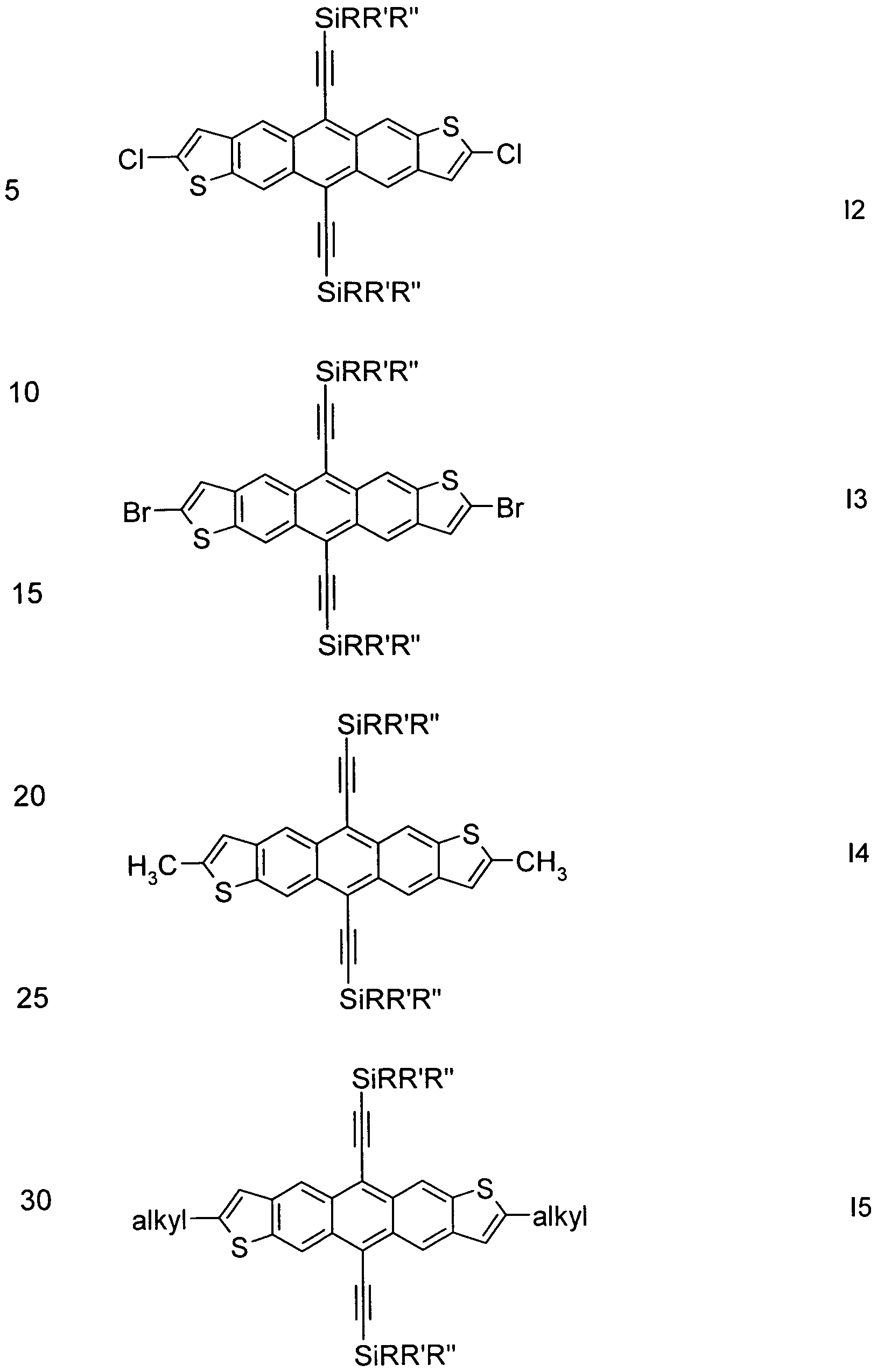


Claims


Priority Applications (7)
| Application Number | Priority Date | Filing Date | Title |
|---|---|---|---|
| KR1020137009092A KR20130103530A (en) | 2010-09-10 | 2011-08-12 | Anthra[2,3-b:7,6-b']dithiophene derivatives and their use as organic semiconductors |
| CN2011800489718A CN103154007A (en) | 2010-09-10 | 2011-08-12 | Anthra[2,3-b:7,6b']dithiophene derivatives and their use as organic semiconductors |
| US13/820,789 US20130161568A1 (en) | 2010-09-10 | 2011-08-12 | Anthra[2,3-b:7,6-b']dithiophene Derivatives and their Use as Organic Semiconductors |
| SG2013016142A SG188395A1 (en) | 2010-09-10 | 2011-08-12 | Anthra[2,3-b:7,6b']dithiophene derivatives and their use as organic semiconductors |
| JP2013527479A JP2013544755A (en) | 2010-09-10 | 2011-08-12 | Anthra [2,3-b: 7,6-b '] dithiophene derivatives and their use as organic semiconductors |
| RU2013115831/04A RU2013115831A (en) | 2010-09-10 | 2011-08-12 | ANTRA [2,3-b: 7,6-b] DITHIOPHENE DERIVATIVES AND THEIR APPLICATION AS ORGANIC SEMICONDUCTORS |
| EP11748268.7A EP2614068A1 (en) | 2010-09-10 | 2011-08-12 | Anthra[2,3-b:7,6b']dithiophene derivatives and their use as organic semiconductors |
Applications Claiming Priority (2)
| Application Number | Priority Date | Filing Date | Title |
|---|---|---|---|
| EP10009454.9 | 2010-09-10 | ||
| EP10009454 | 2010-09-10 |
Publications (1)
| Publication Number | Publication Date |
|---|---|
| WO2012031659A1 true WO2012031659A1 (en) | 2012-03-15 |
Family
ID=44509181
Family Applications (1)
| Application Number | Title | Priority Date | Filing Date |
|---|---|---|---|
| PCT/EP2011/004076 WO2012031659A1 (en) | 2010-09-10 | 2011-08-12 | Anthra[2,3-b:7,6b']dithiophene derivatives and their use as organic semiconductors |
Country Status (9)
| Country | Link |
|---|---|
| US (1) | US20130161568A1 (en) |
| EP (1) | EP2614068A1 (en) |
| JP (1) | JP2013544755A (en) |
| KR (1) | KR20130103530A (en) |
| CN (1) | CN103154007A (en) |
| RU (1) | RU2013115831A (en) |
| SG (1) | SG188395A1 (en) |
| TW (1) | TW201215617A (en) |
| WO (1) | WO2012031659A1 (en) |
Cited By (2)
| Publication number | Priority date | Publication date | Assignee | Title |
|---|---|---|---|---|
| JP2015527741A (en) * | 2012-08-09 | 2015-09-17 | メルク パテント ゲゼルシャフト ミット ベシュレンクテル ハフツングMerck Patent Gesellschaft mit beschraenkter Haftung | Organic semiconductor compound |
| JP2015536041A (en) * | 2012-09-21 | 2015-12-17 | メルク パテント ゲーエムベーハー | Organic semiconductor compound |
Families Citing this family (5)
| Publication number | Priority date | Publication date | Assignee | Title |
|---|---|---|---|---|
| KR101732522B1 (en) | 2014-04-29 | 2017-05-24 | 사빅 글로벌 테크놀러지스 비.브이. | Synthesis of new small molecules/oligomers with high conductivity and absorption for optoelectronic application |
| CN106661058A (en) * | 2014-06-30 | 2017-05-10 | 默克专利股份有限公司 | Extended non-linear acene derivatives and their use as organic semiconductors |
| WO2016035640A1 (en) * | 2014-09-01 | 2016-03-10 | 富士フイルム株式会社 | Organic semiconductor film-forming composition, organic semiconductor film, and organic semiconductor element |
| JP6556844B2 (en) | 2015-08-04 | 2019-08-07 | 富士フイルム株式会社 | Organic thin film transistor and manufacturing method thereof, organic thin film transistor material, organic thin film transistor composition, compound, and organic semiconductor film |
| KR102631401B1 (en) | 2018-08-28 | 2024-01-29 | 삼성전자주식회사 | Compound and thin film transistor and electronic device |
Citations (15)
| Publication number | Priority date | Publication date | Assignee | Title |
|---|---|---|---|---|
| EP0528662A1 (en) | 1991-08-15 | 1993-02-24 | Kabushiki Kaisha Toshiba | Organic field effect transistor |
| US5198153A (en) | 1989-05-26 | 1993-03-30 | International Business Machines Corporation | Electrically conductive polymeric |
| WO1996021659A1 (en) | 1995-01-10 | 1996-07-18 | University Of Technology, Sydney | Organic semiconductor |
| EP0889350A1 (en) | 1997-07-03 | 1999-01-07 | ETHZ Institut für Polymere | Photoluminescent display devices (I) |
| US5892244A (en) | 1989-01-10 | 1999-04-06 | Mitsubishi Denki Kabushiki Kaisha | Field effect transistor including πconjugate polymer and liquid crystal display including the field effect transistor |
| US5998804A (en) | 1997-07-03 | 1999-12-07 | Hna Holdings, Inc. | Transistors incorporating substrates comprising liquid crystal polymers |
| US20030021913A1 (en) | 2001-07-03 | 2003-01-30 | O'neill Mary | Liquid crystal alignment layer |
| US6630566B1 (en) | 1997-12-19 | 2003-10-07 | Avecia Limited | Polymeric material comprising N, P, S, As, or Se and composition for charge transport material |
| US6723394B1 (en) | 1999-06-21 | 2004-04-20 | Cambridge University Technical Services Limited | Aligned polymers for an organic TFT |
| US20040248338A1 (en) | 2001-07-09 | 2004-12-09 | Henning Sirringhaus | Solution influenced alignment |
| US7095044B2 (en) | 2000-11-28 | 2006-08-22 | Merck Patent Gmbh | Field effect transistors and materials and methods for their manufacture |
| US20070102696A1 (en) | 2003-11-28 | 2007-05-10 | Beverley Brown | Organic semiconducting layers |
| US20080128680A1 (en) | 2005-03-08 | 2008-06-05 | Anthony John E | Silylethynylated heteroacenes and electronic devices made therewith |
| WO2008107089A1 (en) | 2007-03-07 | 2008-09-12 | University Of Kentucky Research Foundation | Silylethynylated heteroacenes and electronic devices made therewith |
| WO2009155106A1 (en) | 2008-05-30 | 2009-12-23 | 3M Innovative Properties Company | Silylethynyl pentacene compounds and compositions and methods of making and using the same |
Family Cites Families (4)
| Publication number | Priority date | Publication date | Assignee | Title |
|---|---|---|---|---|
| JP5228907B2 (en) * | 2006-03-10 | 2013-07-03 | コニカミノルタ株式会社 | Organic semiconductor material, organic semiconductor film, organic semiconductor device, and organic thin film transistor |
| JP2007299852A (en) * | 2006-04-28 | 2007-11-15 | Konica Minolta Holdings Inc | Organic semiconductor material, organic semiconductor film, organic semiconductor device, and organic thin film transistor |
| KR101570891B1 (en) * | 2008-03-06 | 2015-11-20 | 메르크 파텐트 게엠베하 | Organic semiconductor formulation |
| KR20100067386A (en) * | 2008-12-11 | 2010-06-21 | 엘지디스플레이 주식회사 | Organic semi-conductor low molecular and organic thin film transistor comprising the same |
-
2011
- 2011-08-12 SG SG2013016142A patent/SG188395A1/en unknown
- 2011-08-12 JP JP2013527479A patent/JP2013544755A/en active Pending
- 2011-08-12 US US13/820,789 patent/US20130161568A1/en not_active Abandoned
- 2011-08-12 EP EP11748268.7A patent/EP2614068A1/en not_active Withdrawn
- 2011-08-12 KR KR1020137009092A patent/KR20130103530A/en not_active Application Discontinuation
- 2011-08-12 RU RU2013115831/04A patent/RU2013115831A/en not_active Application Discontinuation
- 2011-08-12 WO PCT/EP2011/004076 patent/WO2012031659A1/en active Application Filing
- 2011-08-12 CN CN2011800489718A patent/CN103154007A/en active Pending
- 2011-09-09 TW TW100132748A patent/TW201215617A/en unknown
Patent Citations (16)
| Publication number | Priority date | Publication date | Assignee | Title |
|---|---|---|---|---|
| US5892244A (en) | 1989-01-10 | 1999-04-06 | Mitsubishi Denki Kabushiki Kaisha | Field effect transistor including πconjugate polymer and liquid crystal display including the field effect transistor |
| US5198153A (en) | 1989-05-26 | 1993-03-30 | International Business Machines Corporation | Electrically conductive polymeric |
| EP0528662A1 (en) | 1991-08-15 | 1993-02-24 | Kabushiki Kaisha Toshiba | Organic field effect transistor |
| WO1996021659A1 (en) | 1995-01-10 | 1996-07-18 | University Of Technology, Sydney | Organic semiconductor |
| EP0889350A1 (en) | 1997-07-03 | 1999-01-07 | ETHZ Institut für Polymere | Photoluminescent display devices (I) |
| US5998804A (en) | 1997-07-03 | 1999-12-07 | Hna Holdings, Inc. | Transistors incorporating substrates comprising liquid crystal polymers |
| US6630566B1 (en) | 1997-12-19 | 2003-10-07 | Avecia Limited | Polymeric material comprising N, P, S, As, or Se and composition for charge transport material |
| US6723394B1 (en) | 1999-06-21 | 2004-04-20 | Cambridge University Technical Services Limited | Aligned polymers for an organic TFT |
| US7095044B2 (en) | 2000-11-28 | 2006-08-22 | Merck Patent Gmbh | Field effect transistors and materials and methods for their manufacture |
| US20030021913A1 (en) | 2001-07-03 | 2003-01-30 | O'neill Mary | Liquid crystal alignment layer |
| US20040248338A1 (en) | 2001-07-09 | 2004-12-09 | Henning Sirringhaus | Solution influenced alignment |
| US20070102696A1 (en) | 2003-11-28 | 2007-05-10 | Beverley Brown | Organic semiconducting layers |
| US20080128680A1 (en) | 2005-03-08 | 2008-06-05 | Anthony John E | Silylethynylated heteroacenes and electronic devices made therewith |
| US7385221B1 (en) | 2005-03-08 | 2008-06-10 | University Of Kentucky Research Foundation | Silylethynylated heteroacenes and electronic devices made therewith |
| WO2008107089A1 (en) | 2007-03-07 | 2008-09-12 | University Of Kentucky Research Foundation | Silylethynylated heteroacenes and electronic devices made therewith |
| WO2009155106A1 (en) | 2008-05-30 | 2009-12-23 | 3M Innovative Properties Company | Silylethynyl pentacene compounds and compositions and methods of making and using the same |
Non-Patent Citations (24)
| Title |
|---|
| ALCALA, J. APPL. PHYS., vol. 88, 2000, pages 7124 - 7128 |
| C. WEDER ET AL., SCIENCE, vol. 279, 1998, pages 835 - 837 |
| C.M. HANSEN, IND. ENG. AND CHEM., PROD. RES. |
| COAKLEY, K. M., MCGEHEE, M. D., CHEM. MATER., vol. 16, 2004, pages 4533 |
| CROWLEY, J.D., TEAGUE, G.S. JR, LOWE, J.W. JR., JOURNAL OF PAINT TECHNOLOGY, vol. 38, no. 496, 1966, pages 296 |
| D. J. BROER, G. CHALLA, G. N. MOL, MACROMOL. CHEM, vol. 192, 1991, pages 59 |
| D. T. MCQUADE, A. E. PULLEN, T. M. SWAGER, CHEM. REV., vol. 100, 2000, pages 2537 |
| D. WANG, X. GONG, P. S. HEEGER, F. RININSLAND, G. C. BAZAN, A. J. HEEGER, PROC. NATL. ACAD. SCI. U.S.A., vol. 99, 2002, pages 49 |
| DEVL., vol. 9, no. 3, 1970, pages 282 |
| G. YU, J. GAO, J.C. HUMMELEN, F. WUDL, A.J. HEEGER, SCIENCE, vol. 270, 1995, pages 1789 |
| GREEN: "Protective Groups in Organic Synthesis", 1981, JOHN WILEY AND SONS |
| J. E. ANTHONY, CHEM. REV., vol. 106, no. 12, 2006, pages 5028 |
| J. E. ANTHONY, D. L. EATON, S. R. PARKIN, ORG. LETT, vol. 4, 2001, pages 15 |
| L. CHEN, D. W. MCBRANCH, H. WANG, R. HELGESON, F. WUDL, D. G. WHITTEN, PROC. NATL. ACAD. SCI. U.S.A., vol. 96, 1999, pages 12287 |
| LLOYD MATTHEW T ET AL: "Efficient Solution-Processed Photovoltaic Cells Based on an Anthradithiophene/Fullerene Blend", JOURNAL OF THE AMERICAN CHEMICAL SOCIETY, AMERICAN CHEMICAL SOCIETY, WASHINGTON, DC; US, vol. 129, no. 29, 1 January 2007 (2007-01-01), pages 9144 - 9147, XP002478327, ISSN: 0002-7863, [retrieved on 20070627], DOI: 10.1021/JA072147X * |
| M. M. PAYNE, S. R. PARKIN, J. E. ANTHONY, C.-C. KUO, T. N. JACKSON, J. AM. CHEM. SOC., vol. 127, no. 14, 2005, pages 4986 |
| MÜLLER ET AL., SYNTH. METALS, 2000, pages 111 - 112 |
| N. DICESARE, M. R. PINOT, K. S. SCHANZE, J. R. LAKOWICZ, LANGMUIR, vol. 18, 2002, pages 7785 |
| PAYNE MARCIA M ET AL: "Organic Field-Effect Transistors from Solution-Deposited Functionalized Acenes with Mobilities as High as 1 cm2/V.cntdot.s", JOURNAL OF THE AMERICAN CHEMICAL SOCIETY, AMERICAN CHEMICAL SOCIETY, WASHINGTON, DC; US, vol. 127, no. 14, 1 January 2005 (2005-01-01), pages 4986 - 4987, XP002478326, ISSN: 0002-7863, [retrieved on 20050319], DOI: 10.1021/JA042353U * |
| PAYNE MARCIA M ET AL: "Stable, Crystalline Acenedithiophenes with up to Seven Linearly Fused Rings", ORGANIC LETTERS, AMERICAN CHEMICAL SOCIETY, US, vol. 6, no. 19, 1 January 2004 (2004-01-01), pages 3325 - 3328, XP002478325, ISSN: 1523-7060, [retrieved on 20040824], DOI: 10.1021/OL048686D * |
| S. SUBRAMANIAN, S. K. PARK, S. R. PARKIN, V. PODZOROV, T. N. JACKSON, J. E. ANTHONY, J. AM. CHEM. SOC., vol. 130, no. 9, 2008, pages 2706 - 2707 |
| SANKAR SUBRAMANIAN ET AL: "Chromophore Fluorination Enhances Crystallization and Stability of Soluble Anthradithiophene Semiconductors", JOURNAL OF THE AMERICAN CHEMICAL SOCIETY, vol. 130, no. 9, 1 March 2008 (2008-03-01), pages 2706 - 2707, XP055010070, ISSN: 0002-7863, DOI: 10.1021/ja073235k * |
| SOLVENTS, W.H.ELLIS, FEDERATION OF SOCIETIES FOR COATINGS TECHNOLOGY, 1986, pages 9 - 10 |
| WALDAUF ET AL., APPL. PHYS. LETT., vol. 89, 2006, pages 233517 |
Cited By (2)
| Publication number | Priority date | Publication date | Assignee | Title |
|---|---|---|---|---|
| JP2015527741A (en) * | 2012-08-09 | 2015-09-17 | メルク パテント ゲゼルシャフト ミット ベシュレンクテル ハフツングMerck Patent Gesellschaft mit beschraenkter Haftung | Organic semiconductor compound |
| JP2015536041A (en) * | 2012-09-21 | 2015-12-17 | メルク パテント ゲーエムベーハー | Organic semiconductor compound |
Also Published As
| Publication number | Publication date |
|---|---|
| KR20130103530A (en) | 2013-09-23 |
| JP2013544755A (en) | 2013-12-19 |
| RU2013115831A (en) | 2014-10-20 |
| SG188395A1 (en) | 2013-04-30 |
| TW201215617A (en) | 2012-04-16 |
| EP2614068A1 (en) | 2013-07-17 |
| CN103154007A (en) | 2013-06-12 |
| US20130161568A1 (en) | 2013-06-27 |
Similar Documents
| Publication | Publication Date | Title |
|---|---|---|
| EP2560965B1 (en) | Polymers of benzodithiophene and their use as organic semiconductors | |
| EP2464627B1 (en) | Phenanthro[1,10,9,8-c,d,e,f,g]carbazole polymers and their use as organic semiconductors | |
| EP2649082B1 (en) | Non-linear acene derivatives and their use as organic semiconductors | |
| EP2726532B1 (en) | Indaceno derivatives as organic semiconductors | |
| EP2591038A1 (en) | Semiconducting polymers | |
| US9306172B2 (en) | Anthra[2,3-b:7,6-b']dithiophene derivatives and their use as organic semiconductors | |
| WO2008131835A1 (en) | Organic semiconductors | |
| WO2012031659A1 (en) | Anthra[2,3-b:7,6b']dithiophene derivatives and their use as organic semiconductors | |
| US8821762B2 (en) | Anthra[2,3-b]benzo[d]thiophene derivatives and their use as organic semiconductors | |
| US9236574B2 (en) | Dinaphto[2,3-a:2′3′-H]phenazines and their use as organic semiconductors | |
| US9373801B2 (en) | Flavanthrene derivatives and their use as organic semiconductors | |
| EP3160972B1 (en) | Extended non-linear acene derivatives and their use as organic semiconductors |
Legal Events
| Date | Code | Title | Description |
|---|---|---|---|
| WWE | Wipo information: entry into national phase |
Ref document number: 201180048971.8 Country of ref document: CN |
|
| 121 | Ep: the epo has been informed by wipo that ep was designated in this application |
Ref document number: 11748268 Country of ref document: EP Kind code of ref document: A1 |
|
| WWE | Wipo information: entry into national phase |
Ref document number: 2011748268 Country of ref document: EP |
|
| WWE | Wipo information: entry into national phase |
Ref document number: 13820789 Country of ref document: US |
|
| ENP | Entry into the national phase |
Ref document number: 2013527479 Country of ref document: JP Kind code of ref document: A |
|
| NENP | Non-entry into the national phase |
Ref country code: DE |
|
| ENP | Entry into the national phase |
Ref document number: 20137009092 Country of ref document: KR Kind code of ref document: A |
|
| ENP | Entry into the national phase |
Ref document number: 2013115831 Country of ref document: RU Kind code of ref document: A |