WO2015159752A1 - 配線基板 - Google Patents
配線基板 Download PDFInfo
- Publication number
- WO2015159752A1 WO2015159752A1 PCT/JP2015/060768 JP2015060768W WO2015159752A1 WO 2015159752 A1 WO2015159752 A1 WO 2015159752A1 JP 2015060768 W JP2015060768 W JP 2015060768W WO 2015159752 A1 WO2015159752 A1 WO 2015159752A1
- Authority
- WO
- WIPO (PCT)
- Prior art keywords
- metal wiring
- wiring
- transparent
- wiring board
- metal
- Prior art date
- Legal status (The legal status is an assumption and is not a legal conclusion. Google has not performed a legal analysis and makes no representation as to the accuracy of the status listed.)
- Ceased
Links
Images

Classifications
-
- G—PHYSICS
- G06—COMPUTING OR CALCULATING; COUNTING
- G06F—ELECTRIC DIGITAL DATA PROCESSING
- G06F3/00—Input arrangements for transferring data to be processed into a form capable of being handled by the computer; Output arrangements for transferring data from processing unit to output unit, e.g. interface arrangements
- G06F3/01—Input arrangements or combined input and output arrangements for interaction between user and computer
- G06F3/03—Arrangements for converting the position or the displacement of a member into a coded form
- G06F3/041—Digitisers, e.g. for touch screens or touch pads, characterised by the transducing means
- G06F3/044—Digitisers, e.g. for touch screens or touch pads, characterised by the transducing means by capacitive means
- G06F3/0443—Digitisers, e.g. for touch screens or touch pads, characterised by the transducing means by capacitive means using a single layer of sensing electrodes
-
- G—PHYSICS
- G06—COMPUTING OR CALCULATING; COUNTING
- G06F—ELECTRIC DIGITAL DATA PROCESSING
- G06F3/00—Input arrangements for transferring data to be processed into a form capable of being handled by the computer; Output arrangements for transferring data from processing unit to output unit, e.g. interface arrangements
- G06F3/01—Input arrangements or combined input and output arrangements for interaction between user and computer
- G06F3/03—Arrangements for converting the position or the displacement of a member into a coded form
- G06F3/041—Digitisers, e.g. for touch screens or touch pads, characterised by the transducing means
-
- G—PHYSICS
- G06—COMPUTING OR CALCULATING; COUNTING
- G06F—ELECTRIC DIGITAL DATA PROCESSING
- G06F3/00—Input arrangements for transferring data to be processed into a form capable of being handled by the computer; Output arrangements for transferring data from processing unit to output unit, e.g. interface arrangements
- G06F3/01—Input arrangements or combined input and output arrangements for interaction between user and computer
- G06F3/03—Arrangements for converting the position or the displacement of a member into a coded form
- G06F3/041—Digitisers, e.g. for touch screens or touch pads, characterised by the transducing means
- G06F3/044—Digitisers, e.g. for touch screens or touch pads, characterised by the transducing means by capacitive means
- G06F3/0446—Digitisers, e.g. for touch screens or touch pads, characterised by the transducing means by capacitive means using a grid-like structure of electrodes in at least two directions, e.g. using row and column electrodes
Definitions
- the present invention relates to a wiring board, and more particularly to a transparent wiring board in which wiring made of metal nanoparticles is made invisible by chemical treatment.
- an input device having a transparent wiring board is often used in portable devices such as smartphones.
- ITO indium tin oxide
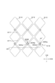
- FIG. 4 is a top view showing a planar configuration of a first translucent electrode pattern and a second translucent electrode pattern formed in a conventional capacitive input device.
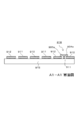
- FIG. 5 is a cross-sectional view of a conventional capacitive input device taken along line A1-A1 ′.
- the conventional capacitance type input device 910 includes a translucent substrate 915, a first translucent electrode pattern 911 made of an ITO film, and a second translucency made of an ITO film.
- An electrode pattern 912, an intersection 918, an interlayer insulating film 904a, and a relay electrode 905a made of an ITO film are provided.
- a first translucent electrode pattern 911 and a second translucent electrode pattern 912 are formed on one surface of the translucent substrate 915. At the intersecting portion 918, the first translucent electrode pattern 911 is connected, while the second translucent electrode pattern 912 is interrupted. Further, as shown in FIGS.
- the second translucent electrode pattern 912 that is interrupted at the intersecting portion 918 is electrically connected by the relay electrode 905a formed in the upper layer of the interlayer insulating film 904a. Yes.
- the translucent electrode pattern 911 and the translucent electrode pattern 912 intersect three-dimensionally at the intersecting portion 918 and flow an independent current in each direction, and thus function as wiring of the capacitive input device.
- the relay electrode 905a in order to form the relay electrode 905a, a process of forming an ITO film using a vacuum process on one surface of the wiring board and an etching process of removing unnecessary portions other than the shape of the relay electrode 905a. And needed.
- the vacuum process since the vacuum process requires a long process time, it is necessary to increase the size of the apparatus in order to maintain the productivity, which increases the manufacturing cost.
- the relay electrode 905a is patterned by the vacuum process and the etching process, much ITO has been consumed separately from the ITO constituting the relay electrode 905a.
- a printed film made of metal nanoparticles represented by silver nanowires is considered promising.
- the patterned thin film made of metal nanoparticles reflects light with a metallic luster on the surface of the metal nanoparticles, so although it is difficult to distinguish with the naked eye, the reflected light is visible depending on the viewing angle. There was a problem.
- the present invention solves the above-mentioned problems, and provides a wiring board on which a transparent wiring is formed by reducing the metallic luster and increasing the invisibility by chemically treating the surface of the metal wiring.
- the wiring board according to claim 1 includes a transparent substrate and a metal wiring formed on the transparent substrate, and a triazine compound having a thiol group is formed on the metal wiring. It has the feature in being.
- the wiring board according to claim 2 is characterized in that the metal wiring is a transparent electrode including metal nanowires.
- the wiring board according to claim 3 is characterized in that the metal wiring contains silver.
- the wiring board according to claim 4 is characterized in that the metal wiring is connected to a plurality of transparent conductive patterns formed on the transparent substrate.
- an insulating film is laminated on a part of the transparent conductive pattern, and a part of the metal wiring is formed on the insulating film, and a plurality of transparent conductive patterns are formed. It is characterized by electrically connecting one of them to the other.
- the wiring board according to claim 6 is characterized in that the triazine compound is triazine trithiol monosodium salt.
- part or all of the metal bonds formed by the metal atoms on the outermost surfaces of the metal wiring are replaced with primary bonds between the metal atoms and the thiol group. While losing a part or all of the gloss, the reflectivity is lowered and it becomes difficult to be visually recognized.
- the metal wiring can be formed substantially transparent, the metal wiring can be hardly seen.
- the metal wiring since silver has a stable conductivity in the atmosphere, the metal wiring obtains a stable conductivity in the atmosphere.
- the wiring board is constituted by the transparent substrate, the transparent conductive pattern, and the metal wiring which is difficult to be visually recognized, it becomes a substantially transparent wiring board.
- the material cost is low, and a strong primary bond is formed between the thiol group and the metal atom on the outermost surface of the metal wiring.
- a highly reliable anti-reflection wiring substrate can be obtained at a low manufacturing cost.
- a wiring board on which a transparent wiring is formed by reducing the metallic luster and increasing the invisibility by chemically treating the surface of the metal wiring.
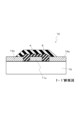
- FIG. 3 is a cross-sectional view taken along the line II ′ of the wiring board according to the first embodiment. It is the measurement result of the reflectance of the visible region-wavelength of the measurement light showing the effect of the antireflection treatment with the triazine compound of the wiring board of the first embodiment. It is a top view which shows the planar structure of the 1st translucent electrode pattern formed in the electrostatic capacitance type input device of a prior art, and a 2nd translucent electrode pattern. It is A1-A1 'sectional drawing of the electrostatic capacitance type input device of a prior art.
- FIG. 1 is a top view showing a planar configuration of the wiring board 1.
- FIG. 2 is a cross-sectional view of the wiring board 1 taken along the line II ′.
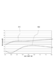
- FIG. 3 shows the measurement result of the reflectance of the visible light region and the wavelength of the measurement light, which shows the effect of the antireflection treatment with the triazine compound of the wiring board 1 of the first embodiment.
- the wiring substrate 1 of the first embodiment generally has a configuration in which transparent electrodes are stretched in a mesh pattern on one surface of a transparent substrate. It can be used as a detector for a type touch panel. The end of the transparent electrode is electrically connected to a device that detects a change in capacitance (Farad), not shown.
- Farad change in capacitance
- the transparent electrode of the wiring board 1 is composed of a first transparent conductive pattern group arranged in parallel at a constant interval and a second transparent electrode arranged in parallel at a fixed interval.
- the conductive pattern group is arranged in a direction perpendicular to each other, thereby forming a mesh shape.
- a square pad portion arranged so as not to overlap with a peripheral pad portion, and the pad portion adjacent to the pad portion. And a thin and short connecting portion that connects the pad portion. Further, the pad portion and the connection portion are continuously arranged along the diagonal extension of the pad portion, thereby forming a linear wiring.
- the portion where the transparent conductive patterns arranged in the orthogonal direction intersect is configured to intersect three-dimensionally, between the transparent conductive patterns, etc. Is provided with an insulating film (insulating film 4). As a result, independent electricity flows through the transparent conductive patterns intersecting each other.
- the pad portion has a shape close to a square as described above, and has a wide dimension within a range that does not overlap with the adjacent pad portion. As a result, when a substance having a large capacitance approaches, the electricity flowing through the transparent conductive pattern is likely to change.
- the transparent substrate 15 is a base material for the detector of the capacitive touch panel. Further, as described above, a transparent conductive pattern is formed on the upper surface of the transparent substrate 15. Thin glass or transparent resin is preferably used for the transparent substrate 15. However, the transparent substrate 15 is transparent, can be in close contact with the transparent conductive pattern, and may be made of a material having strength as a base material of the wiring substrate, and is not limited to thin glass or transparent resin. Absent. When thin glass or transparent resin is used for the transparent substrate 15, the transparent conductive pattern formed on the upper surface of the transparent substrate 15 is subjected to electrostatic induction of the object even when the object approaches from below the transparent substrate 15. The charge becomes polarized.
- the first transparent conductive pattern 11 is a wiring formed on one surface of the transparent substrate 15, and includes a square pad portion 11a and a connection portion 11c formed at a corner of the pad portion 11a. Are connected to each other in a straight line.
- a plurality of first transparent conductive patterns 11 are arranged in parallel at regular intervals to form a comb-like pattern group. Further, as described above, the end of the first transparent conductive pattern 11 is electrically connected to a device that detects a change in capacitance not shown.
- the pad portion 11 a is a part of the first transparent conductive pattern 11 as described above, and is a transparent conductive film having a shape close to a square formed on one surface of the transparent substrate 15.
- the pad portion 11a and the adjacent pad portion 11a are arranged so that one of the diagonal lines of each other overlaps. Moreover, the pad part etc. are arrange
- a connecting portion 11c that electrically connects the corner of the pad portion 11a to the corner of the adjacent pad portion 11a is provided along the diagonal line. ITO is preferably used for the pad portion 11a.
- the pad portion 11a may be made of a transparent conductive material that can be in close contact with the upper surface of the transparent substrate 15 and can be patterned, and is not limited to ITO.
- the pad portion 11a and the connection portion 11c are formed in the same process.
- the connecting portion 11c is a part of the first transparent conductive pattern 11 as described above, and is a thin transparent conductive film formed on one surface of the transparent substrate 15. Further, as described above, the connection portion 11c is provided at the corner of the pad portion 11a along the direction of the first transparent conductive pattern 11, and connects the corner portions of the adjacent pad portions 11a. Is provided. Further, the connection portion 11 c is a part of the intersecting portion 18 where the transparent conductive patterns and the like that intersect perpendicularly intersect as described above, and the upper surface of the connection portion 11 c is in contact with the insulating film 4. ITO is preferably used for the connecting portion 11c.
- the connecting portion 11c may be made of a conductive material that can be in close contact with the upper surface of the transparent substrate 15, can be patterned, and cannot be visually recognized by the naked eye, and is not limited to ITO.
- the pad portion 11a and the connection portion 11c are formed in the same process.
- the second transparent conductive pattern 12 is a wiring formed on one surface of the transparent substrate 15, and is provided in a direction perpendicular to the direction of the first transparent conductive pattern 11.
- the second transparent conductive pattern 12 has a configuration in which pad portions 12a having a shape close to a square and metal wirings 5 that electrically connect corners of the pad portions 12a are alternately connected.
- a plurality of second transparent conductive patterns 12 are arranged in parallel at regular intervals to form a comb-like pattern group.
- the end of the second transparent conductive pattern 12 is electrically connected to a device that detects a change in capacitance (not shown).
- the pad portion 12 a is a part of the second transparent conductive pattern 12 as described above, and is a transparent conductive film having a shape close to a square formed on one surface of the transparent substrate 15.
- the diagonal line of the pad portion 12a and the diagonal line of the adjacent pad portion 12a are arranged so as to overlap each other, and the direction of the diagonal line is perpendicular to the direction in which the first transparent conductive patterns 11 are continuous. ing. Further, the adjacent pad portions 12 a and the like are connected by metal wiring 5 at the corners along the diagonal line.
- ITO is preferably used for the pad portion 12a.
- the pad portion 12a may be made of a conductive material that can be in close contact with the upper surface of the transparent substrate 15, can be patterned, and cannot be visually recognized by the naked eye, and is not limited to ITO.
- the metal wiring 5 is a part of the second transparent conductive pattern 12 as described above, and is a thin transparent conductive film formed on one surface of the transparent substrate 15. Further, as described above, the metal wiring 5 is provided at the corner of the pad portion 12a along the direction of the second transparent conductive pattern 12, and connects the corner portions of the adjacent pad portions 12a. It has become. Further, the metal wiring 5 is a part of the intersecting portion 18 where the transparent conductive patterns or the like that intersect perpendicularly intersect three-dimensionally as described above, and the metal wiring 5 is provided on the upper surface of the insulating film 4. As the metal wiring 5, a transparent conductive thin film mainly composed of silver nanowires is used.
- the outermost surface of the silver nanowire is chemically modified with triazine trithiol monosodium salt.
- the metal wiring 5 can be in close contact with the upper surface of the insulating film 4 and can be printed, and the metal wiring 5 may be any material that contains a metal and is chemically treated with a triazine compound. It is not limited to a thin film mainly composed of chemically modified silver nanowires.
- the wiring board 1 is added to the preparation liquid A (a mixed liquid in which 5 mmol of triazine trithiol monosodium salt and 100 mmol of sodium carbonate are added to pure water and diluted to 1 L) for 10 minutes. Soaked. Moreover, after the wiring board 1 is immersed in the preparation liquid A, it is cleaned by being immersed in pure water, and then blown and dried. As a result, a primary bond is formed between the thiol group of the triazine trithiol monosodium salt and the metal atom on the outermost surface of the metal wiring 5. It is uniformly covered by a sodium salt molecular film.
- the metal bonds on the outermost surface of the metal wiring 5 are replaced with primary bonds with the thiol group of the triazine trithiol monosodium salt, so that the metal wiring 5 loses part or all of the metallic luster. .
- the excess triazine trithiol monosodium salt fixed to the surface layer of the wiring board 1 is dissolved in water, it is removed by immersion in pure water.
- the thickness of the molecular film of triazine trithiol monosodium salt is several tens of nm. For example, even if several layers are laminated, it does not exceed 300 nm.
- the visible light region of the human naked eye is approximately 400 nm to 800 nm, the molecular film of triazine trithiol monosodium salt formed on the outermost surface of the metal wiring 5 is not caught by the human naked eye. Therefore, when the metal wiring 5 is chemically modified with the triazine trithiol monosodium salt, a part or all of the metallic luster is lost while the transparency is maintained.
- the reflectance of the visible light region of the metal wiring 5 is a metal wiring chemically modified with triazine trithiol monosodium salt from the reflectance R1 of the unmodified metal wiring 5 shown in FIG. 5 to reflectivity R2.
- the intersecting portion 18 is an intersecting portion where the orthogonal transparent conductive patterns intersect three-dimensionally, and a part of the transparent substrate 15, the connection portion 11c, the insulating film 4, the metal wiring 5, Part of the pad portion 12 a in contact with the metal wiring 5.
- a connection portion 11 c is provided on a part of the upper surface of the transparent substrate 15.
- An insulating film 4 is provided on the upper surface of the connection portion 11c and the upper surface of a part of the transparent substrate 15 around the connection portion 11c.
- a part of the metal wiring 5 is provided on the upper surface of the insulating film 4.
- the metal wiring 5 is provided from the corner of the pad portion 12a to the corner of the adjacent pad portion 12a across the insulating film 4, and electrically connects the corners of the adjacent pad portions 12a as described above. .
- the insulating film 4 is an insulating film that forms part of the intersecting portion 18 where the transparent conductive patterns or the like that intersect perpendicularly intersect three-dimensionally as described above.
- the insulating film 4 includes the upper surface and side surfaces of the connection portion 11 c, the upper surface of a part of the transparent substrate 15 around the intersection portion 18, and part of the side surface and corner portions of the pad portion 12 a around the intersection portion 18. And an upper surface of the tip.
- a metal wiring 5 is provided on the upper surface of the insulating film 4.
- a transparent resist resin is suitably used for the insulating film 4.
- the insulating film 4 is not limited to a resist resin as long as it is in close contact with the upper surface of the connection portion 11c and the lower surface of the metal wiring 5, is transparent, and is made of a highly insulating material.
- the surface area of the pad portion 11a and the pad portion 12a is large, so that charges accumulate on the surface of the pad portion 11a or the pad portion 12a and polarization occurs. Occur. This increases the capacitance of the transparent conductive pattern.
- the transparent conductive having a changed capacitance is used. The pattern is detected.
- the 1st transparent conductive pattern 11 and the 2nd transparent conductive pattern 12 are the pattern group arrange
- the pad portion 11a, the connecting portion 11c, and the pad portion 12a are made of ITO, the optical characteristics of the wiring board 1 are not adversely affected. Further, since the insulating film 4 is made of a transparent resist resin, the optical characteristics of the wiring board 1 are not adversely affected. Moreover, since the metal wiring 5 is a thin film mainly composed of silver nanowires that have been chemically modified to reduce the metallic luster, the optical characteristics of the wiring board 1 are not adversely affected.
- the wiring substrate 1 of the first embodiment has the transparent substrate 15 and the metal wiring 5 formed on the transparent substrate 15, and the triazine compound having a thiol group is formed on the metal wiring 5. ing. As a result, part or all of the metal bonds formed by the metal atoms on the outermost surface of the metal wiring 5 are replaced with primary bonds between the metal atoms and the thiol group. While losing everything, the reflectivity is reduced and it becomes difficult to see.
- the metal wiring 5 can be formed substantially transparent because the metal wiring 5 is a transparent electrode including metal nanowires, the wiring wiring 1 can be made difficult to be visually recognized.
- the metal wiring 5 contains silver in the wiring board 1, the metal wiring 5 obtains stable conductivity in the atmosphere.
- the wiring board 1 is made of a metal that is difficult to be visually recognized if the metal wiring 5 connecting the plurality of transparent conductive patterns formed on the transparent substrate 15 is made narrow. Therefore, the wiring board is substantially transparent.
- the wiring substrate 1 has an insulating film 4 laminated on a part of the transparent conductive pattern (intersection 18), and the metal wiring 5 is formed on the insulating film 4 so that a plurality of parts are formed.
- One of the transparent conductive patterns is electrically connected to the other one.
- the manufacturing process of the wiring board applicable to an electrostatic capacitance type touch panel can be simplified.
- the insulating film 4 is made of a transparent resist resin, the wiring board 1 does not lose transparency.
- the triazine compound is triazine trithiol monosodium salt in the wiring substrate 1
- the material cost is low, and a strong primary bond is formed between the thiol group and the metal atom on the outermost surface of the metal wiring 5.
- a highly reliable anti-reflection wiring substrate can be obtained at a low manufacturing cost.
- the metal wiring 5 is made of silver, but may be made of a metal other than silver.
- the metal wiring 5 is made of a metal nanowire.
- the metal wire 5 may be made of a metal material having a shape other than the nanowire, for example, a silver nanoparticle having a particle diameter of about several nm to 50 nm. Also good.
- the outermost surface of the silver nanoparticles can be chemically modified with a triazine compound having a thiol group in the same manner as the metal nanowires.
- a fine line pattern made of silver nanoparticles having a particle diameter of about several nanometers to 50 nm is formed sufficiently thin, it is difficult to visually recognize the transmitted light, and the reflectivity decreases due to the effect of the thiol group.
- the visual recognition with reflected light can also be suppressed.
- the volume resistivity of the thin film made of silver nanoparticles does not depend on the direction in which the particles in the thin film are oriented, the metal wiring 5 is formed even when the shape of the metal wiring 5 is bent at a right angle, for example. The volume resistivity does not change.
- the 1st transparent conductive pattern 11 and the 2nd transparent conductive pattern 12 were three-dimensionally crossed, the 1st transparent conductive pattern 11 or the 2nd transparent conductive pattern 12 is a structure other than these. It may intersect with the element.
- the pad portion 11a, the pad portion 12a and the connection portion 11c are made of ITO, but these may be made of metal wiring.
- the insulating film 4 is made of a material (resist resin) other than metal, but may be a layer in which a part (surface) of the metal wiring 5 is made non-conductive. May be.
Landscapes
- Engineering & Computer Science (AREA)
- General Engineering & Computer Science (AREA)
- Theoretical Computer Science (AREA)
- Human Computer Interaction (AREA)
- Physics & Mathematics (AREA)
- General Physics & Mathematics (AREA)
- Position Input By Displaying (AREA)
Abstract
【課題】金属配線の表面を化学処理することによって金属光沢を鈍化させ又不可視性を高めて透明な配線を形成した配線基板を提供する。 【解決手段】透明基板15と、透明基板15上に形成された金属配線5と、を有し、金属配線5の表面にはチオール基を有するトリアジン化合物の層が形成されている。通常の金属配線は、金属光沢によって光が反射するので、配線基板の透明性が損なわれてしまうが、金属配線5は、トリアジン化合物の層を設けることによって、金属光沢が弱まって不可視性が高まるので、希土類を含有しない透明な配線となる。
Description
本発明は、配線基板に関し、特に、金属ナノ粒子からなる配線を化学処理によって不可視化した透明な配線基板に関する。
近年、スマートフォン等の携帯機器では、透明な配線基板を備えた入力装置が使われることが多い。
従来、透明な配線には、インジウムティンオキサイド(以下ITO)等の希土類を含有する材料が用いられてきた。しかし、世界的な希土類の使用量の増加に伴い、資源枯渇が問題視されている。
今後、スマートフォン等の携帯機器の普及に伴い、希土類を使用しない又は希土類の使用量の少ない透明な配線基板が求められている。
従来の配線としては、特許文献1に記載の中継電極をITOエッチングで形成する静電容量型入力装置が知られている。
以下に、従来の静電容量型入力装置について説明する。図4は、従来の静電容量型入力装置に形成された第1の透光性電極パターンおよび第2の透光性電極パターンの平面的な構成を示す上面図である。図5は、従来の静電容量型入力装置のA1-A1′断面図である。
従来の静電容量型入力装置910は、図4に示すように、透光性基板915と、ITO膜からなる第1の透光性電極パターン911と、ITO膜からなる第2の透光性電極パターン912と、交差部分918と、層間絶縁膜904aと、ITO膜からなる中継電極905aと、を備えている。また、透光性基板915の一方の面には、第1の透光性電極パターン911および第2の透光性電極パターン912が形成されている。交差部分918においては、第1の透光性電極パターン911は繋がっている一方、第2の透光性電極パターン912は途切れている。また、交差部分918で途切れている第2の透光性電極パターン912は、図4及び図5に示すように、層間絶縁膜904aの上層に形成された中継電極905aによって電気的に接続されている。また、透光性電極パターン911及び透光性電極パターン912は、交差部分918で立体的に交差し、それぞれの方向に独立した電流を流すので、静電容量型入力装置の配線として機能する。
しかしながら、従来の配線基板では、中継電極905aを形成するために、配線基板の一面に真空プロセスを用いてITOを成膜する工程と、中継電極905aの形状以外の不要な部分を除去するエッチング工程と、を必要としていた。また、特に真空プロセスは、長い工程時間を必要とするので、生産力を維持するためには装置を大型化する必要があり、製造コストが大きくなる原因となっていた。また、真空プロセスと、エッチングプロセスと、によって中継電極905aをパターニングするとき、中継電極905aを構成するITOとは別に、多くのITOが消費されてしまっていた。
ITOの使用量を減らすためには、ITOを使用する工程の全部又は一部を、代替材料を使用する工程に置き換えることが効果的である。
ITO膜の代替材料としては、銀ナノワイヤなどに代表される金属ナノ粒子からなる印刷膜が有望視されている。しかし、金属ナノ粒子からなるパターニングされた薄膜は、金属ナノ粒子の表面で金属光沢によって光が反射するので、肉眼では判別し難いレベルではあるものの、見る角度によっては、反射光が視認されてしまうという課題があった。
本発明は、上述した課題を解決し、金属配線の表面を化学処理することによって金属光沢を鈍化させ又不可視性を高めて透明な配線を形成した配線基板を提供するものである。
この課題を解決するために、請求項1に記載の配線基板は、透明基板と、透明基板上に形成された金属配線とを有し、金属配線上にはチオール基を有するトリアジン化合物が形成されていることに特徴を有する。
また、請求項2記載の配線基板は、金属配線が金属ナノワイヤを含む透明電極であることに特徴を有する。
また、請求項3記載の配線基板は、金属配線が、銀を含むことに特徴を有する。
また、請求項4記載の配線基板は、金属配線は、透明基板上に形成された複数の透明導電パターンとの間を接続することに特徴を有する。
また、請求項5記載の配線基板は、透明導電パターンの一部には絶縁膜が積層されており、金属配線は、その一部が絶縁膜の上に形成されて、複数の透明導電パターンのうちの一つと他の一つとを電気的に接続することに特徴を有する。
また、請求項6記載の配線基板は、トリアジン化合物がトリアジントリチオールモノナトリウム塩であることに特徴を有する。
請求項1の発明によれば、金属配線の最表面の金属原子同士による金属結合の一部または全部は、その金属原子と、チオール基と、の一次結合に置き換えられるので、金属配線は、金属光沢の一部または全部を失うと共に、反射率が低下して視認され難くなる。
請求項2の発明によれば、金属配線を実質的に透明に形成できるため、金属配線を視認され難くすることができる。
請求項3の発明によれば、銀は大気中で安定した導電性があるので、金属配線は大気中で安定した導電性を得る。
請求項4の発明によれば、配線基板は、透明基板と、透明導電パターンと、視認され難い金属配線と、によって構成されるので、実質的に透明な配線基板となる。
請求項5の発明によれば、配線が交差するパターンを形成可能となるので、より複雑な構造の配線基板を得ることができる。また、静電容量型のタッチパネルに適用可能な配線基板の製造工程を簡素化できる。また、絶縁膜に透明な材料を用いれば、配線基板は、透明性を失うことは無い。
請求項6の発明によれば、材料コストは安価となり且つチオール基と金属配線の最表面の金属原子との間には強力な一次結合が形成される。このことによって、安価な製造コストで信頼性の高い反射防止処理を施した配線基板を得ることができる。
以上より、本発明によれば、金属配線の表面を化学処理することによって金属光沢を鈍化させ又不可視性を高めて透明な配線を形成した配線基板を提供できる。
[第1実施形態]
以下、本発明の配線基板を図1及び図2を参照して説明する。図1は、配線基板1の平面的な構成を示す上面図である。図2は、配線基板1のI-I′断面図である。図3は、第1実施形態の配線基板1のトリアジン化合物による反射防止処理の効果を示す可視光領域の反射率-測定光の波長の測定結果である。
以下、本発明の配線基板を図1及び図2を参照して説明する。図1は、配線基板1の平面的な構成を示す上面図である。図2は、配線基板1のI-I′断面図である。図3は、第1実施形態の配線基板1のトリアジン化合物による反射防止処理の効果を示す可視光領域の反射率-測定光の波長の測定結果である。
第1実施形態の配線基板1は、全体的には、図1に示すように、透明基板の片側の面上に、透明電極が網目状に張り巡らされた構成をしており、静電容量型のタッチパネルの検出子として利用できるようになっている。また、その透明電極の端部は、図示していない静電容量(ファラッド)の変化を検出する装置に電気的に接続されている。
また、配線基板1の透明電極は、図1に示すように、一定の間隔で平行に配置された第1の透明導電パターン群と、同様に一定の間隔で平行に配置された第2の透明導電パターン群と、が直交する向きに配置されることによって、網目状に構成されている。
また、配線基板1の透明導電パターンは、そのうちの一本に注目すると、図1に示すように、周辺のパッド部と重ならないように配置された正方形のパッド部と、そのパッド部と隣のパッド部とを繋げる細くて短い接続部分と、を備えている。また、パッド部と接続部分とは、パッド部の対角線の延長線に沿って連続して配置されることによって、直線的な配線を形成している。
また、直交する方向に配置された透明導電パターン同士が交差する部分(交差部分18)は、図1又は図2に示すように、立体交差する構成になっており、その透明導電パターン等の間には絶縁膜(絶縁膜4)が設けられている。このことによって、交差する透明導電パターン等には、それぞれ独立した電気が流れるようになっている。
パッド部は、上述したように正方形に近い形状であると共に、隣のパッド部と重ならない範囲で寸法が広く取られている。このことによって、静電容量の大きい物質が近づいたとき、透明導電パターンに流れる電気は変化し易くなっている。
透明基板15は、上述したように静電容量型のタッチパネルの検出子の基材である。また、上述したように透明基板15の上面には、透明導電パターンが形成されている。透明基板15には、薄いガラスや透明樹脂が好適に用いられる。ただし、透明基板15は、透明であり、又透明導電パターンと密着する事ができ、又配線基板の基材としての強度を備えた材料からなれば良く、薄いガラスまたは透明樹脂に限定するものではない。透明基板15に薄いガラスや透明樹脂を用いると、透明基板15の上面に形成された透明導電パターンは、透明基板15の下方から物体が接近したときにも、その物体の静電誘導を受けて電荷が分極するようになる。
第1の透明導電パターン11は、上述したように、透明基板15の片側の面上に形成された配線であり、正方形のパッド部11aと、パッド部11aの角に形成された接続部分11cと、が連続して繋がることによって直線的な配線になっている。また、複数の第1の透明導電パターン11が一定の間隔を置いて平行に配置されることによって櫛歯状のパターン群を形成している。また、上述したとおり、第1の透明導電パターン11の端は、図示していない静電容量の変化を検出する装置に電気的に接続されている。
パッド部11aは、上述したように第1の透明導電パターン11の一部であり、透明基板15の片側の面上に成形された正方形に近い形状の透明な導電膜である。また、パッド部11aと、その隣のパッド部11aと、は、お互いの対角線の片一方が重なるように配置されている。また、そのパッド部等は、角同士が隣接し、且つ重ならないように配置されている。また、その対角線に沿って、パッド部11aの角からその隣のパッド部11aの角までを電気的に接続する接続部分11cが設けられている。パッド部11aには、ITOが好適に用いられる。ただし、パッド部11aは、透明基板15の上面と密着することのできると共にパターニングすることのできる透明な導電性の材料からなれば良く、ITOに限るものではない。また、パッド部11aと接続部分11cとは同一の工程で形成されている。
接続部分11cは、上述したように第1の透明導電パターン11の一部であり、透明基板15の片側の面上に形成された幅の細い透明な導電膜である。また、接続部分11cは、上述したように、第1の透明導電パターン11の方向に沿って、パッド部11aの角に設けられており、隣り合うパッド部11aの角部同士を接続するように設けられている。また、接続部分11cは、上述したように直行する透明導電パターン等が立体的に交差する交差部分18の一部であり、接続部分11cの上面は、絶縁膜4と接している。接続部分11cには、ITOが好適に用いられる。ただし、接続部分11cは、透明基板15の上面と密着することのでき、又パターニングすることのでき、又肉眼で視認することのできない導電性の材料からなれば良く、ITOに限るものではない。また、パッド部11aと接続部分11cとは同一の工程で形成されている。
第2の透明導電パターン12は、上述したように、透明基板15の片側の面上に形成された配線であり、第1の透明導電パターン11の方向とは直行する方向に設けられている。また、第2の透明導電パターン12は、正方形に近い形状のパッド部12aと、パッド部12aの角同士を電気的に接続する金属配線5と、が交互に接続された構成になっている。また、複数の第2の透明導電パターン12が一定の間隔を置いて平行に配置されることによって櫛歯状のパターン群を形成している。また、上述したとおり、第2の透明導電パターン12の端は、図示していない静電容量の変化を検出する装置に電気的に接続されている。
パッド部12aは、上述したように第2の透明導電パターン12の一部であり、透明基板15の片側の面上に成形された正方形に近い形状の透明な導電膜である。また、パッド部12aの対角線とその隣のパッド部12aの対角線とは、重なるように配置されており、その対角線の方向は、第1の透明導電パターン11が連なっている方向に対して直行している。また、隣り合うパッド部12a等は、その対角線に沿って角部同士が金属配線5によって接続されている。パッド部12aには、ITOが好適に用いられる。ただし、パッド部12aは、透明基板15の上面と密着することのでき、又パターニングすることのでき、又肉眼で視認することのできない導電性の材料からなれば良く、ITOに限るものではない。
金属配線5は、上述したように第2の透明導電パターン12の一部であり、透明基板15の片側の面上に形成された幅の細い透明な導電膜である。また、金属配線5は、上述したように、第2の透明導電パターン12の方向に沿って、パッド部12aの角に設けられており、隣り合うパッド部12aの角部同士を接続するようになっている。また、金属配線5は、上述したように直行する透明導電パターン等が立体的に交差する交差部分18の一部であり、金属配線5は、絶縁膜4の上面に設けられている。金属配線5は、銀ナノワイヤを主成分とする透明導電薄膜が用いられている。また、その銀ナノワイヤの最表面は、トリアジントリチオールモノナトリウム塩によって化学修飾されている。ただし、金属配線5は、絶縁膜4の上面と密着することのでき、又印刷することのでき、又金属を含むと共にその金属の表面はトリアジン化合物で化学処理されている材料であれば良く、化学修飾された銀ナノワイヤを主成分とした薄膜に限るものではない。
また、金属配線5が化学修飾されるとき、配線基板1は、調製液A(トリアジントリチオールモノナトリウム塩5mmol及び炭酸ソーダ100mmolを純水に加えて全量を1Lに希釈した混合液)に10分間浸漬される。また、配線基板1は、調製液Aへの浸漬後に、純水に浸漬されることによって洗浄されてから送風乾燥される。このことによって、トリアジントリチオールモノナトリウム塩のチオール基と、金属配線5の最表面の金属原子と、の間には一次結合が形成されるので、金属配線5の最表面は、トリアジントリチオールモノナトリウム塩の分子膜によって万遍なく被覆される。また、金属配線5の最表面の金属結合の一部または全部は、トリアジントリチオールモノナトリウム塩のチオール基との一次結合に置き換えられるので、金属配線5は、金属光沢の一部または全部を失う。また、配線基板1の表層に固着した余剰のトリアジントリチオールモノナトリウム塩は水に溶解するので、純水への浸漬によって除去される。また、トリアジントリチオールモノナトリウム塩の分子膜の厚さは、数十nmであり、例えば、数層積層したとしても300nmを超えることは無い。また、人の肉眼の可視光領域は、およそ400nm~800nmなので、金属配線5の最表面に形成されたトリアジントリチオールモノナトリウム塩の分子膜は、人の肉眼に捉えられることは無い。従って、金属配線5は、トリアジントリチオールモノナトリウム塩よって化学修飾されるとき、透明性は保たれたまま、金属光沢の一部または全部が失われた状態になる。
また、金属配線5の可視光領域の反射率は、化学修飾の影響によって、図3に示す、無修飾の金属配線5の反射率R1から、トリアジントリチオールモノナトリウム塩によって化学修飾された金属配線5の反射率R2へと変わる。
交差部分18は、上述したように、直交する透明導電パターン同士が立体的に交差する交差部分であり、透明基板15の一部と、接続部分11cと、絶縁膜4と、金属配線5と、金属配線5に接しているパッド部12aの一部と、を備えて構成されている。透明基板15の一部の上面に、接続部分11cが設けられている。また、接続部分11cの上面と、その周囲の透明基板15の一部の上面と、には絶縁膜4が設けられている。また、絶縁膜4の上面には金属配線5の一部が設けられている。金属配線5は、絶縁膜4を跨いでパッド部12aの角から隣のパッド部12aの角まで設けられており、上述したように隣り合うパッド部12aの角同士を電気的に接合している。
絶縁膜4は、上述したように直行する透明導電パターン等が立体的に交差する交差部分18の一部を形成する絶縁膜である。また、絶縁膜4は、接続部分11cの上面及び側面と、交差部分18の周辺の透明基板15の一部の上面と、交差部分18の周辺のパッド部12aの側面の一部及び角部の先端の上面と、に設けられている。また、絶縁膜4の上面には、金属配線5が設けられている。絶縁膜4には、透明なレジスト樹脂が好適に用いられる。ただし、絶縁膜4は、接続部分11cの上面及び金属配線5の下面と密着し、又透明であり、又絶縁性の高い材料からなれば良く、レジスト樹脂に限るものではない。
(第1実施形態の作用)
次に、本発明である配線基板1の作用について説明する。
次に、本発明である配線基板1の作用について説明する。
第1実施形態の配線基板1は、静電容量の大きな物体が近づくとき、パッド部11a及びパッド部12aの表面積は大きいので、パッド部11a又はパッド部12aの表面には電荷が溜まって分極が起こる。このことによって、透明導電パターンの静電容量は大きくなる。また、第1の透明導電パターン11と、第2の透明導電パターン12と、の端は静電容量の変化を検出する装置に電気的に接続されているので、静電容量の変化した透明導電パターンは検知される。また、第1の透明導電パターン11と、第2の透明導電パターン12と、は直行する方向に櫛歯状に配置されたパターン群であるので、静電容量の変化した透明導電パターンの位置を特定することによって、物体の接近した位置を特定することができる。
また、パッド部11a及び接続部分11c及びパッド部12aは、ITOからなるので、配線基板1の光学特性に悪影響を与えない。また、絶縁膜4は透明なレジスト樹脂からなるので、配線基板1の光学特性に悪影響を与えない。また、金属配線5は、金属光沢を鈍化する化学修飾の施された銀ナノワイヤを主成分とする薄膜なので、配線基板1の光学特性に悪影響を与えない。
尚、静電容量の大きな物体が近づくときに、パッド部の表面で起こる静電容量(ファラッド)の変化は、一般的な物理化学の現象であるので、作用及び解析方法の説明は割愛する。
以上から、第1実施形態の配線基板1は、透明基板15と、透明基板15上に形成された金属配線5と、を有し、金属配線5上にはチオール基を有するトリアジン化合物が形成されている。このことによって、金属配線5の最表面の金属原子同士による金属結合の一部または全部は、その金属原子とチオール基との一次結合に置き換えられるので、金属配線5は、金属光沢の一部または全部を失うと共に、反射率が低下して視認され難くなる。
また、配線基板1は、金属配線5が金属ナノワイヤを含む透明電極であることによって、金属配線5を実質的に透明に形成できるため、金属配線5を視認され難くすることができる。
また、配線基板1は、金属配線5が、銀を含むので、金属配線5は大気中で安定した導電性を得る。
また、配線基板1は、透明基板15上に形成された複数の透明導電パターン等の間を接続する金属配線5を細幅にすれば、透明基板15と、透明導電パターンと、視認され難い金属配線5と、によって構成されるので、実質的に透明な配線基板となる。
また、配線基板1は、透明導電パターンの一部(交差部分18)には絶縁膜4が積層されており、金属配線5は、その一部が絶縁膜4の上に形成されて、複数の透明導電パターンのうちの一つと他の一つとを電気的に接続されている。このことによって、配線が交差するパターンを形成可能となるので、より複雑なパターンの実質的に透明な配線基板を得ることができる。また、静電容量型のタッチパネルに適用可能な配線基板の製造工程を簡素化できる。また、絶縁膜4は、透明なレジスト樹脂からなるので、配線基板1は、透明性を失うことは無い。
また、配線基板1は、トリアジン化合物がトリアジントリチオールモノナトリウム塩であるので、材料コストは安価となり且つチオール基と金属配線5の最表面の金属原子との間には強力な一次結合が形成される。このことによって、安価な製造コストで信頼性の高い反射防止処理を施した配線基板を得ることができる。
なお、本発明は上記実施形態に限定されるものではなく、例えば次のように変形して実施することができ、これらの実施形態も本発明の技術的範囲に属する。
上記実施形態では、金属配線5は、銀からなっていたが、銀以外の金属からなっていてもよい。
上記実施形態では、金属配線5は、金属ナノワイヤからなっていたが、ナノワイヤ以外の形状の金属材料からなっていても良く、例えば、粒子径が数nm~50nm程度の銀ナノ粒子からなっていても良い。銀ナノ粒子の最表面は、金属ナノワイヤと同様にチオール基を有するトリアジン化合物によって化学修飾することができる。また、粒子径が数nm~50nm程度の銀ナノ粒子からなる細線パターンは十分に細く形成すると、透過光では視認しづらく形成することができ、またチオール基の効果で反射率が低下することにより、反射光での視認も抑制することができる。このことによれば、銀ナノ粒子からなる薄膜の体積抵抗率は、薄膜内の粒子の配向する方向に依存しなくなるので、金属配線5の形状を、例えば、直角に曲げた時にも金属配線5の体積抵抗率が変わることは無い。
上記実施形態では、第1の透明導電パターン11と第2の透明導電パターン12とが立体交差していたが、第1の透明導電パターン11又は第2の透明導電パターン12は、これら以外の構成要素と立体交差していてもよい。
上記実施形態では、パッド部11a及びパッド部12a及び接続部分11cはITOからなっていたが、これらは金属配線からなっていてもよい。
上記実施形態では、絶縁膜4は、金属以外の材料(レジスト樹脂)からなっていたが、金属配線5の一部(表面)を不導体化した層であってもよい。
てもよい。
てもよい。
その他、本発明は要旨を逸脱しない範囲で種々変更して実施することができる。
1 配線基板(上位構造)
4 絶縁膜(請求項記載の部材名称)
5 金属配線(請求項記載の部材名称)
11 第1の透明導電パターン
11c 接続部分
12 第2の透明導電パターン
12a パッド部
15 透明基板(請求項記載の部材名称)
18 交差部分
R1 無修飾の金属配線5の反射率
R2 トリアジントリチオールモノナトリウム塩によって化学修飾された金属配線5の反射率
4 絶縁膜(請求項記載の部材名称)
5 金属配線(請求項記載の部材名称)
11 第1の透明導電パターン
11c 接続部分
12 第2の透明導電パターン
12a パッド部
15 透明基板(請求項記載の部材名称)
18 交差部分
R1 無修飾の金属配線5の反射率
R2 トリアジントリチオールモノナトリウム塩によって化学修飾された金属配線5の反射率
Claims (6)
- 透明基板と、前記透明基板上に形成された金属配線とを有し、前記金属配線上にはチオール基を有するトリアジン化合物が形成されている、ことを特徴とする配線基板。
- 前記金属配線が金属ナノワイヤを含む透明電極である、ことを特徴とする請求項1に記載の配線基板。
- 前記金属配線が、銀を含む、ことを特徴とする請求項1に記載の配線基板。
- 前記金属配線は、前記透明基板上に形成された複数の透明導電パターンとの間を接続する、ことを特徴とする請求項1及び請求項2または請求項3に記載の配線基板。
- 前記透明導電パターンの一部には絶縁膜が積層されており、前記金属配線は、その一部が前記絶縁膜の上に形成されて、複数の透明導電パターンのうちの一つと他の一つとを電気的に接続する、ことを特徴とする請求項4の配線基板。
- 前記トリアジン化合物がトリアジントリチオールモノナトリウム塩である、ことを特徴とする請求項1から請求項5のいずれかに記載の座標入力装置。
Priority Applications (1)
| Application Number | Priority Date | Filing Date | Title |
|---|---|---|---|
| JP2016513725A JP6194414B2 (ja) | 2014-04-15 | 2015-04-06 | 配線基板 |
Applications Claiming Priority (2)
| Application Number | Priority Date | Filing Date | Title |
|---|---|---|---|
| JP2014-083896 | 2014-04-15 | ||
| JP2014083896 | 2014-04-15 |
Publications (1)
| Publication Number | Publication Date |
|---|---|
| WO2015159752A1 true WO2015159752A1 (ja) | 2015-10-22 |
Family
ID=54323963
Family Applications (1)
| Application Number | Title | Priority Date | Filing Date |
|---|---|---|---|
| PCT/JP2015/060768 Ceased WO2015159752A1 (ja) | 2014-04-15 | 2015-04-06 | 配線基板 |
Country Status (2)
| Country | Link |
|---|---|
| JP (1) | JP6194414B2 (ja) |
| WO (1) | WO2015159752A1 (ja) |
Citations (2)
| Publication number | Priority date | Publication date | Assignee | Title |
|---|---|---|---|---|
| JP2007329302A (ja) * | 2006-06-08 | 2007-12-20 | Iwate Univ | 電磁波シールド基板の製造方法 |
| JP2013077235A (ja) * | 2011-09-30 | 2013-04-25 | Fujifilm Corp | 電極パターン、タッチパネル、液晶表示装置及び、有機elディスプレイ |
-
2015
- 2015-04-06 JP JP2016513725A patent/JP6194414B2/ja not_active Expired - Fee Related
- 2015-04-06 WO PCT/JP2015/060768 patent/WO2015159752A1/ja not_active Ceased
Patent Citations (2)
| Publication number | Priority date | Publication date | Assignee | Title |
|---|---|---|---|---|
| JP2007329302A (ja) * | 2006-06-08 | 2007-12-20 | Iwate Univ | 電磁波シールド基板の製造方法 |
| JP2013077235A (ja) * | 2011-09-30 | 2013-04-25 | Fujifilm Corp | 電極パターン、タッチパネル、液晶表示装置及び、有機elディスプレイ |
Also Published As
| Publication number | Publication date |
|---|---|
| JPWO2015159752A1 (ja) | 2017-04-13 |
| JP6194414B2 (ja) | 2017-09-06 |
Similar Documents
| Publication | Publication Date | Title |
|---|---|---|
| TWI628565B (zh) | 導電片、靜電容式觸控面板以及顯示裝置 | |
| CN105579937B (zh) | 触摸面板用电极、触摸面板以及显示装置 | |
| CN105765501B (zh) | 导电片、静电电容式触摸面板和显示装置 | |
| KR102427146B1 (ko) | 터치 센서 기판, 터치 패널, 표시 장치 및 터치 센서 기판의 제조 방법 | |
| KR101676546B1 (ko) | 터치 패널 센서 | |
| CN109799935A (zh) | 触控感应单元 | |
| TWI661253B (zh) | 透明電極構件及其之製造方法、以及使用該透明電極構件的靜電電容式感測器 | |
| KR20150084458A (ko) | 터치 패널 | |
| KR20130072402A (ko) | 터치패널의 전극형성방법 | |
| CN203930742U (zh) | 纳米银线导电层叠结构及触控面板 | |
| CN103176660B (zh) | 位置传感器 | |
| KR101775894B1 (ko) | 투명 발열 필름 및 이의 제조 방법 | |
| CN111699461A (zh) | 透明电极构件、层叠透明电极构件以及静电电容式传感器 | |
| KR102275704B1 (ko) | 터치 패널 및 그 제조 방법 | |
| CN203930771U (zh) | 一种触控面板 | |
| JP6194414B2 (ja) | 配線基板 | |
| JP6405298B2 (ja) | 静電容量式センサ、タッチパネルおよび電子機器 | |
| CN203849707U (zh) | 触控面板 | |
| CN104637573B (zh) | 导电薄膜结构 | |
| US9089061B2 (en) | Conductive film, method for making the same, and touch screen including the same | |
| CN207302018U (zh) | 导电膜基板、触摸屏传感器及模块 | |
| KR20130115692A (ko) | 터치 패널의 전극 패턴 | |
| CN108958547B (zh) | 一种触控面板及制备方法 | |
| KR102056097B1 (ko) | 편광 가변형 소자 및 이의 제조방법 | |
| CN111742286A (zh) | 透明电极构件、层叠透明电极构件及静电电容式传感器 |
Legal Events
| Date | Code | Title | Description |
|---|---|---|---|
| 121 | Ep: the epo has been informed by wipo that ep was designated in this application |
Ref document number: 15779706 Country of ref document: EP Kind code of ref document: A1 |
|
| ENP | Entry into the national phase |
Ref document number: 2016513725 Country of ref document: JP Kind code of ref document: A |
|
| NENP | Non-entry into the national phase |
Ref country code: DE |
|
| 122 | Ep: pct application non-entry in european phase |
Ref document number: 15779706 Country of ref document: EP Kind code of ref document: A1 |