WO2015159705A1 - 荷電粒子線装置および検査装置 - Google Patents
荷電粒子線装置および検査装置 Download PDFInfo
- Publication number
- WO2015159705A1 WO2015159705A1 PCT/JP2015/060205 JP2015060205W WO2015159705A1 WO 2015159705 A1 WO2015159705 A1 WO 2015159705A1 JP 2015060205 W JP2015060205 W JP 2015060205W WO 2015159705 A1 WO2015159705 A1 WO 2015159705A1
- Authority
- WO
- WIPO (PCT)
- Prior art keywords
- line
- pattern
- charged particle
- sample
- edge
- Prior art date
- Legal status (The legal status is an assumption and is not a legal conclusion. Google has not performed a legal analysis and makes no representation as to the accuracy of the status listed.)
- Ceased
Links
Images







Classifications
-
- G—PHYSICS
- G03—PHOTOGRAPHY; CINEMATOGRAPHY; ANALOGOUS TECHNIQUES USING WAVES OTHER THAN OPTICAL WAVES; ELECTROGRAPHY; HOLOGRAPHY
- G03F—PHOTOMECHANICAL PRODUCTION OF TEXTURED OR PATTERNED SURFACES, e.g. FOR PRINTING, FOR PROCESSING OF SEMICONDUCTOR DEVICES; MATERIALS THEREFOR; ORIGINALS THEREFOR; APPARATUS SPECIALLY ADAPTED THEREFOR
- G03F1/00—Originals for photomechanical production of textured or patterned surfaces, e.g., masks, photo-masks, reticles; Mask blanks or pellicles therefor; Containers specially adapted therefor; Preparation thereof
- G03F1/20—Masks or mask blanks for imaging by charged particle beam [CPB] radiation, e.g. by electron beam; Preparation thereof
-
- G—PHYSICS
- G03—PHOTOGRAPHY; CINEMATOGRAPHY; ANALOGOUS TECHNIQUES USING WAVES OTHER THAN OPTICAL WAVES; ELECTROGRAPHY; HOLOGRAPHY
- G03F—PHOTOMECHANICAL PRODUCTION OF TEXTURED OR PATTERNED SURFACES, e.g. FOR PRINTING, FOR PROCESSING OF SEMICONDUCTOR DEVICES; MATERIALS THEREFOR; ORIGINALS THEREFOR; APPARATUS SPECIALLY ADAPTED THEREFOR
- G03F7/00—Photomechanical, e.g. photolithographic, production of textured or patterned surfaces, e.g. printing surfaces; Materials therefor, e.g. comprising photoresists; Apparatus specially adapted therefor
- G03F7/70—Microphotolithographic exposure; Apparatus therefor
- G03F7/70058—Mask illumination systems
- G03F7/7015—Details of optical elements
-
- G—PHYSICS
- G03—PHOTOGRAPHY; CINEMATOGRAPHY; ANALOGOUS TECHNIQUES USING WAVES OTHER THAN OPTICAL WAVES; ELECTROGRAPHY; HOLOGRAPHY
- G03F—PHOTOMECHANICAL PRODUCTION OF TEXTURED OR PATTERNED SURFACES, e.g. FOR PRINTING, FOR PROCESSING OF SEMICONDUCTOR DEVICES; MATERIALS THEREFOR; ORIGINALS THEREFOR; APPARATUS SPECIALLY ADAPTED THEREFOR
- G03F7/00—Photomechanical, e.g. photolithographic, production of textured or patterned surfaces, e.g. printing surfaces; Materials therefor, e.g. comprising photoresists; Apparatus specially adapted therefor
- G03F7/70—Microphotolithographic exposure; Apparatus therefor
- G03F7/70216—Mask projection systems
- G03F7/70275—Multiple projection paths, e.g. array of projection systems, microlens projection systems or tandem projection systems
-
- G—PHYSICS
- G03—PHOTOGRAPHY; CINEMATOGRAPHY; ANALOGOUS TECHNIQUES USING WAVES OTHER THAN OPTICAL WAVES; ELECTROGRAPHY; HOLOGRAPHY
- G03F—PHOTOMECHANICAL PRODUCTION OF TEXTURED OR PATTERNED SURFACES, e.g. FOR PRINTING, FOR PROCESSING OF SEMICONDUCTOR DEVICES; MATERIALS THEREFOR; ORIGINALS THEREFOR; APPARATUS SPECIALLY ADAPTED THEREFOR
- G03F7/00—Photomechanical, e.g. photolithographic, production of textured or patterned surfaces, e.g. printing surfaces; Materials therefor, e.g. comprising photoresists; Apparatus specially adapted therefor
- G03F7/70—Microphotolithographic exposure; Apparatus therefor
- G03F7/70483—Information management; Active and passive control; Testing; Wafer monitoring, e.g. pattern monitoring
-
- G—PHYSICS
- G03—PHOTOGRAPHY; CINEMATOGRAPHY; ANALOGOUS TECHNIQUES USING WAVES OTHER THAN OPTICAL WAVES; ELECTROGRAPHY; HOLOGRAPHY
- G03F—PHOTOMECHANICAL PRODUCTION OF TEXTURED OR PATTERNED SURFACES, e.g. FOR PRINTING, FOR PROCESSING OF SEMICONDUCTOR DEVICES; MATERIALS THEREFOR; ORIGINALS THEREFOR; APPARATUS SPECIALLY ADAPTED THEREFOR
- G03F7/00—Photomechanical, e.g. photolithographic, production of textured or patterned surfaces, e.g. printing surfaces; Materials therefor, e.g. comprising photoresists; Apparatus specially adapted therefor
- G03F7/70—Microphotolithographic exposure; Apparatus therefor
- G03F7/708—Construction of apparatus, e.g. environment aspects, hygiene aspects or materials
- G03F7/7085—Detection arrangement, e.g. detectors of apparatus alignment possibly mounted on wafers, exposure dose, photo-cleaning flux, stray light, thermal load
-
- H—ELECTRICITY
- H01—ELECTRIC ELEMENTS
- H01J—ELECTRIC DISCHARGE TUBES OR DISCHARGE LAMPS
- H01J37/00—Discharge tubes with provision for introducing objects or material to be exposed to the discharge, e.g. for the purpose of examination or processing thereof
- H01J37/02—Details
- H01J37/244—Detectors; Associated components or circuits therefor
-
- H—ELECTRICITY
- H01—ELECTRIC ELEMENTS
- H01J—ELECTRIC DISCHARGE TUBES OR DISCHARGE LAMPS
- H01J37/00—Discharge tubes with provision for introducing objects or material to be exposed to the discharge, e.g. for the purpose of examination or processing thereof
- H01J37/26—Electron or ion microscopes; Electron or ion diffraction tubes
- H01J37/28—Electron or ion microscopes; Electron or ion diffraction tubes with scanning beams
-
- H—ELECTRICITY
- H01—ELECTRIC ELEMENTS
- H01J—ELECTRIC DISCHARGE TUBES OR DISCHARGE LAMPS
- H01J37/00—Discharge tubes with provision for introducing objects or material to be exposed to the discharge, e.g. for the purpose of examination or processing thereof
- H01J37/26—Electron or ion microscopes; Electron or ion diffraction tubes
- H01J37/285—Emission microscopes, e.g. field-emission microscopes
-
- H—ELECTRICITY
- H10—SEMICONDUCTOR DEVICES; ELECTRIC SOLID-STATE DEVICES NOT OTHERWISE PROVIDED FOR
- H10P—GENERIC PROCESSES OR APPARATUS FOR THE MANUFACTURE OR TREATMENT OF DEVICES COVERED BY CLASS H10
- H10P74/00—Testing or measuring during manufacture or treatment of wafers, substrates or devices
-
- H—ELECTRICITY
- H10—SEMICONDUCTOR DEVICES; ELECTRIC SOLID-STATE DEVICES NOT OTHERWISE PROVIDED FOR
- H10P—GENERIC PROCESSES OR APPARATUS FOR THE MANUFACTURE OR TREATMENT OF DEVICES COVERED BY CLASS H10
- H10P74/00—Testing or measuring during manufacture or treatment of wafers, substrates or devices
- H10P74/20—Testing or measuring during manufacture or treatment of wafers, substrates or devices characterised by the properties tested or measured, e.g. structural or electrical properties
- H10P74/203—Structural properties, e.g. testing or measuring thicknesses, line widths, warpage, bond strengths or physical defects
-
- H—ELECTRICITY
- H10—SEMICONDUCTOR DEVICES; ELECTRIC SOLID-STATE DEVICES NOT OTHERWISE PROVIDED FOR
- H10P—GENERIC PROCESSES OR APPARATUS FOR THE MANUFACTURE OR TREATMENT OF DEVICES COVERED BY CLASS H10
- H10P76/00—Manufacture or treatment of masks on semiconductor bodies, e.g. by lithography or photolithography
- H10P76/40—Manufacture or treatment of masks on semiconductor bodies, e.g. by lithography or photolithography of masks comprising inorganic materials
- H10P76/405—Manufacture or treatment of masks on semiconductor bodies, e.g. by lithography or photolithography of masks comprising inorganic materials characterised by their composition, e.g. multilayer masks
-
- H—ELECTRICITY
- H10—SEMICONDUCTOR DEVICES; ELECTRIC SOLID-STATE DEVICES NOT OTHERWISE PROVIDED FOR
- H10P—GENERIC PROCESSES OR APPARATUS FOR THE MANUFACTURE OR TREATMENT OF DEVICES COVERED BY CLASS H10
- H10P76/00—Manufacture or treatment of masks on semiconductor bodies, e.g. by lithography or photolithography
- H10P76/40—Manufacture or treatment of masks on semiconductor bodies, e.g. by lithography or photolithography of masks comprising inorganic materials
- H10P76/408—Manufacture or treatment of masks on semiconductor bodies, e.g. by lithography or photolithography of masks comprising inorganic materials characterised by their sizes, orientations, dispositions, behaviours or shapes
- H10P76/4083—Manufacture or treatment of masks on semiconductor bodies, e.g. by lithography or photolithography of masks comprising inorganic materials characterised by their sizes, orientations, dispositions, behaviours or shapes characterised by their behaviours during the lithography processes, e.g. soluble masks or redeposited masks
-
- H—ELECTRICITY
- H10—SEMICONDUCTOR DEVICES; ELECTRIC SOLID-STATE DEVICES NOT OTHERWISE PROVIDED FOR
- H10P—GENERIC PROCESSES OR APPARATUS FOR THE MANUFACTURE OR TREATMENT OF DEVICES COVERED BY CLASS H10
- H10P76/00—Manufacture or treatment of masks on semiconductor bodies, e.g. by lithography or photolithography
- H10P76/40—Manufacture or treatment of masks on semiconductor bodies, e.g. by lithography or photolithography of masks comprising inorganic materials
- H10P76/408—Manufacture or treatment of masks on semiconductor bodies, e.g. by lithography or photolithography of masks comprising inorganic materials characterised by their sizes, orientations, dispositions, behaviours or shapes
- H10P76/4085—Manufacture or treatment of masks on semiconductor bodies, e.g. by lithography or photolithography of masks comprising inorganic materials characterised by their sizes, orientations, dispositions, behaviours or shapes characterised by the processes involved to create the masks
-
- H—ELECTRICITY
- H10—SEMICONDUCTOR DEVICES; ELECTRIC SOLID-STATE DEVICES NOT OTHERWISE PROVIDED FOR
- H10P—GENERIC PROCESSES OR APPARATUS FOR THE MANUFACTURE OR TREATMENT OF DEVICES COVERED BY CLASS H10
- H10P76/00—Manufacture or treatment of masks on semiconductor bodies, e.g. by lithography or photolithography
- H10P76/40—Manufacture or treatment of masks on semiconductor bodies, e.g. by lithography or photolithography of masks comprising inorganic materials
- H10P76/408—Manufacture or treatment of masks on semiconductor bodies, e.g. by lithography or photolithography of masks comprising inorganic materials characterised by their sizes, orientations, dispositions, behaviours or shapes
- H10P76/4088—Processes for improving the resolution of the masks
-
- H—ELECTRICITY
- H01—ELECTRIC ELEMENTS
- H01J—ELECTRIC DISCHARGE TUBES OR DISCHARGE LAMPS
- H01J2237/00—Discharge tubes exposing object to beam, e.g. for analysis treatment, etching, imaging
- H01J2237/22—Treatment of data
- H01J2237/221—Image processing
-
- H—ELECTRICITY
- H01—ELECTRIC ELEMENTS
- H01J—ELECTRIC DISCHARGE TUBES OR DISCHARGE LAMPS
- H01J2237/00—Discharge tubes exposing object to beam, e.g. for analysis treatment, etching, imaging
- H01J2237/245—Detection characterised by the variable being measured
- H01J2237/24592—Inspection and quality control of devices
-
- H—ELECTRICITY
- H01—ELECTRIC ELEMENTS
- H01J—ELECTRIC DISCHARGE TUBES OR DISCHARGE LAMPS
- H01J2237/00—Discharge tubes exposing object to beam, e.g. for analysis treatment, etching, imaging
- H01J2237/26—Electron or ion microscopes
- H01J2237/28—Scanning microscopes
- H01J2237/2809—Scanning microscopes characterised by the imaging problems involved
-
- H—ELECTRICITY
- H01—ELECTRIC ELEMENTS
- H01J—ELECTRIC DISCHARGE TUBES OR DISCHARGE LAMPS
- H01J2237/00—Discharge tubes exposing object to beam, e.g. for analysis treatment, etching, imaging
- H01J2237/26—Electron or ion microscopes
- H01J2237/28—Scanning microscopes
- H01J2237/2813—Scanning microscopes characterised by the application
- H01J2237/2814—Measurement of surface topography
-
- H—ELECTRICITY
- H01—ELECTRIC ELEMENTS
- H01J—ELECTRIC DISCHARGE TUBES OR DISCHARGE LAMPS
- H01J2237/00—Discharge tubes exposing object to beam, e.g. for analysis treatment, etching, imaging
- H01J2237/26—Electron or ion microscopes
- H01J2237/28—Scanning microscopes
- H01J2237/2813—Scanning microscopes characterised by the application
- H01J2237/2817—Pattern inspection
-
- H—ELECTRICITY
- H01—ELECTRIC ELEMENTS
- H01J—ELECTRIC DISCHARGE TUBES OR DISCHARGE LAMPS
- H01J2237/00—Discharge tubes exposing object to beam, e.g. for analysis treatment, etching, imaging
- H01J2237/30—Electron or ion beam tubes for processing objects
- H01J2237/317—Processing objects on a microscale
- H01J2237/3175—Lithography
- H01J2237/31761—Patterning strategy
- H01J2237/31762—Computer and memory organisation
Definitions
- the present invention relates to a charged particle beam apparatus and an inspection apparatus.
- a new technology for forming patterns with smaller pitches has been introduced because the typical dimensions of patterns (hereinafter referred to as CD) are 30 nm or less.
- CD typical dimensions
- a typical one is a process called Self-aligned double patterning (SADP).
- SADP Self-aligned double patterning
- this method after a resist pattern is formed by conventional lithography, a film is formed on the entire surface, and etching is performed to form a pattern on the side wall of the resist pattern. Thereby, it is possible to form a dense pattern having a pitch that is half the pitch of the pattern created by the first lithography.
- FIG. 1 is a schematic cross-sectional view of a pattern for explaining a process of forming fine lines and spaces using SAQP.
- 1 (a) to 1 (f) show the process of forming a line pattern by the first SADP
- FIGS. 1 (g) to 1 (i) form the line pattern by the second SADP. The process is shown.
- a resist layer 121 patterned in a line shape is formed on the silicon oxide film 126, the silicon nitride film 125, the silicon oxide film 124, the carbon film 123, and the antireflection film 122, which are sequentially stacked from the bottom (FIG. 1A). )).
- a silicon oxide film 131 is formed so as to cover the resist layer 121 (FIG. 1B). Note that although there is only one resist layer 121 in the drawing, a large number of resist layers are actually formed.
- the silicon oxide film 131 is anisotropically etched to form line-shaped silicon oxide films 131 on both sides of the resist layer 121 (FIG. 1C).
- the resist layer 121 is removed by ashing or the like (FIG. 1D).
- the laminated film of the antireflection film 122 and the carbon film 123 is etched anisotropically to form a line-shaped laminated film (FIG. 1E).
- the antireflection film 122 is removed (FIG. 1 (f)). Thereby, it is possible to form a dense pattern having a pitch that is half the pitch of the pattern created by the first lithography.
- the silicon oxide film 141 is etched by anisotropic dry etching, so that the line-shaped silicon oxide film 141 is formed on both sides of the carbon film 123. It is formed (FIG. 1 (g)).
- the carbon film 123 is removed (FIG. 1 (h)).
- anisotropic etching is performed using the silicon oxide film 141 as a mask to form a laminated film of the line-shaped silicon oxide film 124 and the silicon nitride film 125 (FIG. 1 (i)).
- the pitch can be further divided with respect to the pattern formed by SADP.
- the said material is an example and is not limited to the said material.
- Fig. 1 (i) shows the final pattern shape, but there is also a possibility that pattern inspection may be performed after removing the etching mask material remaining at the top of the line.
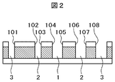
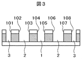
- reference numerals 1, 2 and 3 indicate space portions in the final shape.
- Reference numerals 101 to 108 denote the edges of the line pattern to be noted.
- one line formed by conventional lithography first becomes four lines. For this reason, the characteristics of the line and space patterns (CD and edge irregularities) fluctuate with a period of 4 lines and spaces.
- the center of the space corresponds to the center of the resist line pattern formed by the first lithography (mandrel: in FIG. 1)
- the space portion indicated by reference numeral 1) is referred to as an initial core.
- the portion where the film deposited on the outer side of the first resist pattern side wall finally becomes a space is defined as a second core (space portion indicated by reference numeral 2 in FIG. 1), and a space that is neither of these. Is defined as a gap (space portion indicated by reference numeral 3 in FIG. 1).
- FIG. 2 shows a case where the CD of the last formed line pattern is not uniform.
- the phenomenon in which thick and thin lines alternate as shown in FIG. 2 may be seen when film deposition with anisotropy occurs during film formation.
- FIG. 3 shows a case where the space CD is not uniform. There are various causes for this, which will be described later.
- a normal wafer manager pays attention to the dimension of the line pattern. In this case, even if the dimension of the line pattern is correct, the position of the line is shifted.
- CD-SEM scanning electron microscope
- the reason why inspection is difficult is that a large number of processes are required until a final pattern is obtained, so that a dimensional abnormality related to a plurality of process problems occurs.
- the dimension inspection it is necessary not only to detect a dimension abnormality but also to obtain a clue for identifying the process that caused the abnormality.
- An index or algorithm for pointing out the problem is required from the pattern data resulting from a plurality of processes.
- the SAQP process has a problem of misalignment in addition to detecting dimensional anomalies and estimating problem processes.
- the variation of the space CD causes the following problems.
- the pattern position at the time of the first resist pattern formation is as designed, that is, when it can be formed at an appropriate position with respect to the lower layer pattern, it is determined that the amount of overlay between layers is sufficiently small, and due to this overlay deviation We expect that the degradation of device performance is small.
- the line pattern position is shifted as a result of SAQP, the positional shift between the individual pattern and the lower layer or upper layer pattern is large. Since the overlay deviation is not recognized at the time of pattern exposure, there is a possibility of causing an unexpected element failure. However, a method for detecting this has not yet been found.
- the first is a technique for distinguishing line patterns and space patterns that look the same but are formed by different processes. For this purpose, it is only necessary to identify the position where the first resist pattern occupied, that is, where the initial core corresponds, among the four types of space patterns that all look the same.
- the simplest method for realizing the first technology is to widen the imaging range and place the end of the line pattern group in one image.
- this method is used, an area that does not fit within the imaging range of one image cannot be inspected.
- a method of increasing the size of the image can be considered, improvement of hardware is required to realize this.
- Patent Document 1 In the case of the SADP pattern, the method shown in Patent Document 1 has been proposed.
- SAQP there are three types of space patterns: initial core, second core, and gap.
- initial core In the case of SAQP, only the core and gap are used.
- an edge formed by depositing a film on the outer side of the core that is, an edge sandwiching the gap, utilizes a phenomenon that unevenness is reduced as compared with the left and right edges of the core region.
- Edge irregularities that is, line edge roughness, are calculated for each edge, the left and right edges of the space are paired, the average of the LER of the edges belonging to the pair is calculated, and the pair of edges having a large LER value is judged to belong to the core .
- Patent Document 1 The inventors examined the possibility of applying the method of Patent Document 1 to SAQP. As a result, it seemed possible to apply this method to SAQP in principle. However, as a result of examining this method in more detail, the problem that the reliability of judgment deteriorates was found.
- the edge property Assuming that the LER is transferred to a smaller value every time the film is formed, the LER of the edge 103 and 106, which is the result of transferring the edge formed by the first lithography in FIG. Edges 102 and 107 resulting from the transfer of the film formed in the second film formation have a smaller LER. Further, the edges 101 and 108 formed by the second film formation have LERs smaller than the edges 102 and 107, and the edges 104 and 105 have LERs smaller than the edges 103 and 106. As described in Patent Document 1, attention is paid to a space, and it is considered to take an average of LERs of both edges sandwiching the space.
- the LER does not always decrease in the same manner in the first and second film formation. If the LER reduction effect in the second film formation is large, the LER average value of the edge sandwiching the initial core and the LER average value of the edge sandwiching the gap appear to be approximately the same. Third, as a result of lithography or etching, the LER may be slightly different between the left and right edges. Even in such a case, the difference becomes invisible by averaging the LER. For these reasons, the position of the initial core is often mistaken for a gap when applied to an actual pattern.
- Patent Document 1 is not used to specify the initial core, it may be used only for the second SADP part, that is, only the second core is specified. There is. Although it can be distinguished if it is observed at the stage of FIG. 1 (h), at the stage of FIG. 1 (i), the conditions for etching and resist removal are appropriate, and all line patterns have the same cross-sectional shape. When the surface of the base is formed so as to have the same physical property, the side wall shape of the edges 101, 104, 105, and 108 is equal to the side wall shape of the edges 102, 103, 106, and 107. Even at the stage of FIG. 1 (h), as long as the influence of film deposition is small and the roundness of the top is small, the distinction is not possible as in FIG. 1 (i). Therefore, even in the second core identification according to the application of Patent Document 1, the probability of the judgment is lowered.
- An object of the present invention is to provide a charged particle beam apparatus and an inspection apparatus capable of specifying the position of an initial core with high accuracy even in a fine line & space pattern formed by using SADP multiple times.
- a charged particle source A plurality of lines formed by covering the line-shaped first pattern formed on the laminated film and performing film deposition to form a line-shaped second pattern on both side walls of the first pattern twice or more.
- a sample stage on which a sample having a line pattern is placed;
- An irradiation optical system for irradiating the sample placed on the sample stage with charged particles emitted from the charged particle source as a charged particle beam;
- a detector for detecting secondary charged particles emitted from the sample by irradiation of the charged particle beam;
- a display unit for displaying image data of the surface of the sample obtained based on the signal of the secondary charged particles detected by the detector; Based on the image data, a calculation unit that calculates a line edge roughness value that is an index of unevenness of line edges of a plurality of line-shaped patterns arranged adjacent to each other in the sample;
- a charged particle beam apparatus comprising: a determination unit that compares the line edge roughness values in the plurality of line-shaped patterns and determine
- a charged particle source The sample is formed by covering the line-shaped first pattern formed on the laminated film and performing film deposition to form a line-shaped second pattern on both side walls of the first pattern twice or more.
- a sample stage on which a sample having a plurality of line-shaped patterns is placed;
- An irradiation optical system for irradiating the sample placed on the sample stage with charged particles emitted from the charged particle source as a charged particle beam;
- a detector for detecting secondary charged particles emitted from the sample by irradiation of the charged particle beam;
- a display unit for displaying image data of the surface of the sample obtained based on the signal of the secondary charged particles detected by the detector; Based on the image data, a calculation unit that calculates the similarity of the left and right edge shapes of a plurality of adjacent spaces arranged in the sample;
- a determination unit that determines a position of a second core that is the second pattern formed on both sides of the first pattern based on the similarity between the left and right edge shapes in the line
- a charged particle source A plurality of lines formed by covering the line-shaped first pattern formed on the laminated film and performing film deposition to form a line-shaped second pattern on both side walls of the first pattern twice or more.
- An irradiation optical system for irradiating the sample placed on the sample stage with charged particles emitted from the charged particle source as a charged particle beam;
- a detector for detecting secondary charged particles emitted from the sample by irradiation of the charged particle beam;
- a display unit for displaying image data of the surface of the sample obtained based on the signal of the secondary charged particles detected by the detector;
- a similarity calculator that calculates the similarity of the shape of the center variation of adjacent lines as the center variation of the line;
- a position determination unit that determines the position of the line-shaped pattern formed before the last film deposition based on the similarity of the uneven shape of the edge or the similarity of the shape of the center variation of the line;
- a roughness value calculation unit that calculates a line edge roughness value that is an index of unevenness of line edges of the plurality of line-shaped patterns arranged adjacent to each other;
- An initial core determination unit that determines the position of the initial core that is the center of the first pattern based on the position of the line-shaped pattern formed before the last film deposition and the line edge roughness value.
- a display unit that displays image data of a surface of the sample obtained by irradiating a sample having a plurality of line-shaped patterns with a charged particle beam; and on the left and right sides of a plurality of spaces arranged adjacent to each other based on the image data
- a calculation unit for calculating the similarity of the edge shape A determination unit that determines the position of a second core that is the second pattern formed on both sides of the first pattern based on the similarity between the left and right edge shapes in the line pattern or the space, It is set as the inspection apparatus characterized by having.
- a similarity calculator that calculates the similarity of the shape of the center variation of adjacent lines as the center variation of the line;
- a position determination unit that determines the position of the line-shaped pattern formed before the last film deposition based on the similarity of the uneven shape of the edge or the similarity of the shape of the center variation of the line;
- a roughness value calculation unit that calculates a line edge roughness value that is an index of unevenness of line edges of the plurality of line-shaped patterns arranged adjacent to each other;
- An initial core determining unit that determines the position of the initial core that is the center of the first pattern based on the position of the line-shaped pattern formed before the final film deposition and the line edge roughness value; The inspection device.
- the position of the initial core can be specified even for a pattern formed by using SADP multiple times.
- FIG. 4 is a schematic cross-sectional view when a film is deposited so as to cover a sidewall of a fine pattern. It is a pattern cross-sectional schematic diagram which shows the location measured by this invention. It is an example of the flowchart for specifying the initial core specification demonstrated in the 1st Example of this invention.
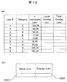
- FIG. 1 It is an example of a table or the like displayed on the operation terminal screen in the second embodiment of the present invention, (a) is a table showing the center position of each pattern when the x-axis origin, and (b) is a line pattern The input screen of the design value of the pitch and the overlay deviation amount is shown. It is an example of the table
- FIG. 6 is a schematic cross-sectional view of a pattern showing a fine pattern processing step to which the present invention is applied in the third embodiment of the present invention, wherein (a) to (c) are pattern formation steps by the first SADP, and (d) to (d) (e) shows the second pattern formation process by SADP, and (f) to (g) show the third pattern formation process by SADP.
- It is a schematic diagram of the observation image obtained in the 3rd Example of this invention. It is an example of the table of the LER value calculated in the 3rd Example of this invention, and displayed on the operating terminal screen.
- the present invention obtains the distribution of the LER value of the pattern edge from the CD-SEM image that does not include the end of the line pattern group, the similarity of the shape of the left and right edges of the space, or along the line at the center position of the adjacent line.
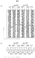
- FIG. 4A A CD-SEM image as shown in FIG. 4A is acquired, and in the image, the direction parallel to the line is y, and the vertical direction is x.
- FIG. 4A A cross-sectional view of the observation object corresponding to the CD-SEM image of FIG. 4A is shown in FIG.
- the diagonal lattice pattern portion in FIG. 4A corresponds to a space area.
- the line pattern edges in the image are numbered. For example, numbers 1, 2,... Are assigned from the left side to the right side of the image. However, in FIG. 4, the edge numbers 1, 2, 3,... Are distinguished from the numbers in the other drawings by reference numerals 401, 402, 403, 404, 405, 406, 407, 408, 409, 410. It is written.
- edges with the same numbers in FIGS. 4A and 4B mean the same edges. Odd numbers are left edges of lines, and even numbers are right edges. Reference numerals 412, 414, 416, 418, and 420 indicate line portions, and reference numerals 411, 413, 415, 417, 419, and 421 indicate space portions.
- the edge number is E_n.
- a set of edge points representing each line edge is obtained by image processing.
- the edge points constituting the edge with the edge number E_n are represented as a set of x coordinates. That is, ⁇ x (i, E_n)
- i 1, 2, 3... P_n ⁇ .
- the line edge is defined by P_n points.
- This amount is a function of the line edge number E_n and the number of points within the edge (in many cases the points are numbered in order from the smallest y coordinate). Also, the y coordinate y (i, E_n) of the i-th edge point is
- the line edge is approximated by a straight line, and the deviation of the x coordinate of each edge point from this approximate straight line is assumed to be ⁇ x (i, E_n).
- the roughness of the E_n-th line edge is represented by a set of deviation amounts ⁇ x (i, E_n)
- i 1, 2, 3... P_n ⁇ .
- LER value is the size of the unevenness of one edge obtained from this set. The most commonly used value is three times the standard deviation as defined below.
- the value 3 on the left side is set to 1, 2, or 6, and the difference between the maximum value and the minimum value of ⁇ x (i, E_n) belonging to a certain edge may be used as the LER value. .
- ⁇ _c (L_n) is a standard deviation of ⁇ x_c (i, L_n)
- i 1, 2, 3... P_n ⁇ .
- the pattern formation process is as shown in FIG. It is possible to add a step of embedding a silicon oxide film or the like in a gap between the formed patterns, that is, a space portion, and removing the original line portion while leaving the silicon oxide film by etching. This makes it possible to reverse the relationship between the line and the space, that is, so-called positive-negative inversion, but here, in order to simplify the explanation, it is assumed that all the core patterns are removed.
- the following method may be performed by exchanging the relationship between some lines and spaces.
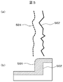
- FIG. 5A is a schematic top view of the edge of the line pattern obtained by depositing a film on the core pattern, etching to expose the core portion, and further removing the core.
- FIG. 5B is a schematic diagram of a cross section when a film is deposited on the core pattern. Edges using the same numbers in FIGS. 5A and 5B correspond to each other.
- reference numeral 501 indicated by a broken line is a line edge corresponding to the surface of the deposited film
- reference numeral 502 indicated by a solid line is a line edge of the core pattern.
- the left edge 501 of the line in FIG. 5B has irregularities similar to the right edge 502. However, in general, fine irregularities are smoothed when a film is deposited. Therefore, the LER of the left edge 501 is smaller than the LER of the right edge 502. This is hereinafter referred to as an LER transfer model.
- the LER of the edge 501 may be larger than the LER of the edge 502 because the film deposition process condition is rarely optimized. In such a case, the film thickness is not uniformly deposited, so the final device performance that can be achieved may be significantly lower.
- LER is obtained according to (Equation 2) for the eight edges 101 to 108 arranged in the center shown in FIG. 1 (i) as an initial core.
- LER values are small, medium, large, medium, medium, large, medium, small.
- the gap between the portions where the edges with medium LER are arranged is the initial core, and the gap between the edges where the edges with small LER are arranged.
- the position of the initial core can be known.
- Patent Document 1 even if an attempt is made to directly compare a medium LER portion and a small portion, the difference is small.
- an edge having a large LER value and a small edge are specified. Specifically, first, a number is assigned to a plurality of edges from one direction to another in the image. When creating a sequence of LER values, the values are always arranged according to the order of the numbers. Next, assuming the initial core position, the edge number dependence of the LER value magnitude (distribution of three types of large, medium, and small values) predicted based on that assumption and the actual LER measurement value edge The number dependence is compared, and the degree of similarity between the two is calculated to determine whether or not they match. This can be done by changing the position of the assumed initial core. The edge where the LER becomes large does not face the initial core or the gap, but if this edge can be identified, it will be known where the initial core is as a whole. Hereinafter, this method is referred to as a first method for specifying an initial core.
- the above method can be modified as follows. First, as in the above-described method, the edges are numbered from one direction to the other direction in the image. When creating a sequence of LER values, the values are always arranged according to the order of the numbers.
- a new LER value is obtained only by the LER measurement value of the edge that should have a large LER and the LER measurement value of the edge that should have a small LER under that assumption. And determine whether it is equal to the expected distribution of LER values (large and small binary distributions). This can be done by changing the position of the assumed initial core. This correction increases calculation time but improves determination accuracy. This method is good when priority is given to determination accuracy over calculation time.
- this method is referred to as a second method for specifying the initial core.
- the space where high similarity was obtained is the second core. Furthermore, there is a method for improving the accuracy of determination rather than simply determining a space with a high degree of similarity as a second core.
- the space arranged side by side is a repetition of the second core, the initial core, the second core, and the gap.
- the similarity between the left and right edge shapes is not increased in the initial core and the gap. Specifically, numbers are assigned in the order in which the spaces are arranged, and the space number dependency of the similarity between the left and right edges of the space is obtained. Then, the space number dependency of this similarity should be repeated large and small, and the portion corresponding to the large becomes the second core.
- the above invention is more accurate than the method in which the method shown in Patent Document 1 is applied to SAQP and the initial core is not specified and only the second core is specified. This is because it is desirable that the lines formed by film deposition have a symmetrical shape from the beginning, so that the lines are made symmetrical by devising the etching process. In this case, in the signal waveform, the difference between the original edge and the edge created by film deposition is very small. However, since the size of the LER remains, the use of the present invention increases the accuracy of specifying the second core.
- the space is numbered 1, 2, 3,...
- the space number corresponding to the second core is 1 and 3 (mod 4) or 2 and 0 according to the method using the similarity between the left and right edges of the space described above. You can see which is (mod4). Therefore, the initial core candidates are narrowed down to two cases: 2 or 0 (mod 4) in the former case and 1 or 3 (mod 4) in the latter case. If an attempt is made to obtain an initial core by skipping this process, the probabilities must be evaluated for all of the initial cores of spaces 1, 2, 3, and 4, and a correct answer must be derived from the four. However, by narrowing down to two candidates first, identification with higher accuracy can be performed. This method requires a longer calculation time than the method of directly obtaining the initial core, but the accuracy is improved.
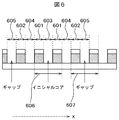
- the most basic indicator is the width of the final line pattern. This is referred to as CDL_final below.
- the second film formation process is omitted in FIG. 1 and is performed between FIG. 1 (f) and FIG. 1 (g). If the film is uniformly deposited, the final CD_final is formed. Is constant regardless of the line number. However, periodic changes in CDL_final may appear due to differences in the chemical properties of the underlying surface and the distribution of distances between the second core patterns. Therefore, we propose the width of the line that sandwiches the initial core, CDL_finalcore and the width of the line that sandwiches the gap, and CDL_finalgap.
- CDL_finalcore and CDL_finalgap instead of the average value of simple line width CDL_final.
- the former is the dimension of the line formed at the position where the resist pattern was originally present, and the latter is the dimension of the line formed at the position originally in the space area. In other words, since they are formed through different processes, if there is a difference between these amounts, the influence of the original resist pattern can be seen.
- the space pattern width is an important dimension index.
- the periodic change of this value is mainly due to the non-uniformity of the film in the first film forming process. The cause of such heterogeneity is the same as in the case of CDL_final described above.
- This index itself is the same as the space width measured in the past, but can be distinguished if the position of the initial core is known. If the initial core space width is CDS_initcore, the second core space width is CDS_2ndcore, and the gap space width is CDS_gap, the effects of the process can be separated by comparing these values. If there are multiple data, take the average value. For example, if CDS_2ndcore is an abnormally small value, it means that the film deposition amount was insufficient in the first film formation (details will be described in Examples).
- Reference numeral 601 is CDL_finalcore
- reference numeral 602 is CDL_finalgap
- reference numeral 603 is CDS_initcore
- reference numeral 604 is CDS_2ndcore
- reference numeral 605 is CDS_gap.
- CD_core indicated by reference numeral 606 and CD_gap indicated by reference numeral 607 in FIG.
- the former corresponds to the resist pattern dimension formed first, but it is not completely equal to the initial resist pattern dimension because of the etching process and the like. These two are used to determine whether a dimension or pattern position abnormality is related to the initial resist pattern dimension. As for this index, if data can be acquired from a plurality of locations, an average may be taken.
- the effective overlay error can be calculated if the initial core can be identified.
- the edge formed by transferring the edge of the first resist pattern can be specified.
- two edges giving CD_core indicated by reference numeral 606 are shown. The center of these two edges is set as a reference point on the x coordinate.
- the x coordinate of the center of each line pattern is obtained, and the overlay error calculated when the first resist pattern is formed is calculated from this reference point. What is necessary is just to add deviation
- the present invention it is possible to estimate a problem of a process from a final pattern image created by a SAQP process that has not been possible so far, and to evaluate an overlay error of each pattern. Since it calculates the LER of each edge in the image, the correlation value of the edge shape, and the distance between specific edges, there is no need to image the end of the line pattern group, and the area important for device performance is directly inspected. be able to. Further, since it is only necessary to take an image with a field of view of about several hundreds of nanometers on one side, the imaging time can be the same as in the past.
- the storage area for storing the image is also the same as the conventional one. That is, it is possible to evaluate a process that has not been possible so far without deteriorating cost and throughput.
- the present invention will be described in detail with reference to examples.
- pattern length measurement and inspection may be performed by another apparatus, for example, a general-purpose scanning electron microscope may be used, an ion microscope or a transmission microscope. It is possible to use charged particle beam apparatuses such as a scanning electron microscope and a scanning transmission electron microscope. Further, if a calculation device using the obtained pattern information can be used, the device need not necessarily be integrated with the charged particle beam device.
- the target to be detected by the detector is mainly described by taking secondary electrons as an example, it should be mentioned in advance that it can be realized by detecting charged particles such as reflected electrons, mirror electrons, and ions emitted from a sample.
- the initial core is specified with emphasis on accuracy rather than calculation time, and further dimension measurement is performed to estimate process problems and improve yield.
- An example will be described.
- FIG. 7 shows a flowchart for specifying the initial core used in this embodiment
- FIG. 8 shows a conceptual diagram of a scanning electron microscope including the configuration of the sample observation apparatus and analysis system used in this embodiment.
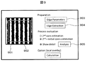
- 9, 10, and 11 are schematic diagrams of windows that appear when the present invention is implemented and two graphs on the monitor screen during image analysis.
- FIG. 12 shows a cross-sectional view in the process of pattern formation estimated as a result of application of the present invention.
- FIG. 13 shows an example of a diagram in which a table of results finally obtained is displayed on the operation terminal screen.
- a fine line & pattern image was obtained using SAQP before the flow of FIG.
- a sample (sample) 807 is placed on a sample stage (sample stage) 808 of a scanning electron microscope, and an electron beam 803 emitted from an electron gun 802 is converted into an electron optical system (irradiation optics) including lenses 804 and 806 and a deflector 805.
- the secondary electrons 809 generated from the sample are detected by a detector (detection optical system) 810, a control system 811 of each part of the scanning electron microscope, and a sample observation apparatus and an analysis system terminal (In other words, the calculation unit that calculates the result obtained from the detector as image data) 812 stores image data based on the detection signal in the data storage device 813.
- Reference numeral 801 denotes a casing of a scanning electron microscope.
- the operator operated the terminal of the image analysis device 814 that can transmit and receive data from the scanning electron microscope including the sample observation device and the analysis system, and operated the program for specifying the initial core (step S701).
- the image data is called from the data storage device 813 and displayed on the monitor screen of the image analysis device 814 (step S702). That is, the image analysis device 814 includes an input / output unit 815 for calling up image data from the data storage device 813, a determination unit 816 that operates a program for determining an initial core, a second core, and the like, and a display unit that displays the determination result 817.
- a display unit may be provided on the terminal (calculation unit) 812 of the analysis system.
- the input / output unit and the determination unit may be incorporated in a scanning electron microscope, an image analysis device, or other devices as long as the problem of the present application is solved.
- step S703 sets an area to be analyzed on the image 901.
- the set area is indicated by a dashed frame 902.
- step S704 the operator proceeds to step S704 and inputs the definition of the edge.
- the Edge Parameters button 903 shown on the screen was clicked.
- a parameter setting window for defining the edge of the line pattern appeared, and the operator entered the definition of the edge there.
- step S705 clicks the Edge Extraction button 904 to extract an edge.
- numbers (1, 2, 3, 4, 5) were assigned from the left on the line pattern in the broken line frame (analysis region) 902 of the image 901. These numbers correspond to the line patterns 412, 414, 416, 418, 420 shown in FIG.
- the edge was displayed as a set of points on the image.
- step S706 selects whether to obtain only the second core or obtain the initial core after obtaining the second core in the core identification algorithm. It chose to seek the initial core after obtaining a second core, and click on the selection symbol to the left display of the 2 nd + initial cores estimation. I also wanted to display the ⁇ _s and LER values calculated when specifying the core, so I clicked on the selection symbol on the left of the Show detail display.
- the initial core is obtained after obtaining the second core.
- an algorithm for obtaining the initial core can be directly used.
- ⁇ x (E_n, i) is obtained from the position information of the edges of lines 1 to 5 (edge number E_n takes a value of 1 to 10 and corresponds to edges 401 to 410 shown in FIG. 4).
- ⁇ _s was obtained for the spaces of space numbers 1 to 4 (corresponding to spaces 411, 413, 415, and 417 in FIG. 4) according to (Equation 3).
- the space number is equal to the line number on the left.
- the L_n dependency of ⁇ _s was displayed as a graph on the operation terminal screen. This graph is shown in FIG.
- the image analysis apparatus 814 applies this result to repetition of large and small values, and since ⁇ _s of the space 2 (right of the line 2 in the screen) and the space 4 is large, it is determined that these are second cores (step S707).
- the image analysis apparatus 814 calculated LER from 10 edges according to (Equation 2).
- the dependency of the LER on the edge number E_n is displayed in a graph on the operation terminal screen. This graph is shown in FIG.
- the image analysis device 814 proceeds to step S708 to identify the initial core.
- the image analysis apparatus 814 determines that the space 3 is the initial core, displays “initial core: space 3” in the upper right area of the image 901, and further displays “correlation value 0.85” (step S708). .
- the correlation value of all candidates may be obtained and the position of the initial core may be specified by the candidate whose value is the maximum value. Since correlation values may differ greatly (in this case, -0.10 and 0.85), instead of obtaining correlation values for all candidates, a threshold is set for the correlation value, and candidates that exceed the threshold are identified. At that time, the position of the initial core can be specified by the candidate.
- the operator knows that the lines 1, 4, and 5 are the lines that sandwich the gap, and the lines 2 and 3 are the lines that sandwich the initial core, and when measuring each line width, the average width of the lines that sandwich the gap is 19.51nm, the average line width across the initial core was 16.38nm. All design dimensions are 18nm. From this, it was found that the dimensions of the pattern in the region where the resist pattern was initially formed differed from the pattern in the region where the resist pattern was not initially formed. As a result of the examination, it took a short time in the step of removing the resist next to FIG. 1 (d), so the resist remained slightly, and the state shown in FIG. 1 (e) should be changed to the original state as shown in FIG. It was found that the film remained at the position. On this film, the components of the film that was formed the second time were particularly difficult to deposit, so the line that sandwiched the initial core was eventually thinner.
- FIG. 1 This is a calculation example from one image, but it is incorporated into a measurement recipe, and data from multiple images is compiled into a table in the format shown in FIG. 13 and output to a medium designated as a text file or storage device 813. Can also be stored.
- the present embodiment it is possible to provide a scanning electron microscope and an inspection apparatus capable of specifying the position of the initial core with high accuracy even in a fine line & space pattern formed by using SADP a plurality of times.
- various indicators of dimensions such as the space of the initial core, it is possible to estimate process problems and improve the process from the final pattern image produced by using the SADP process multiple times.
- FIG. 14 is a schematic diagram of a window that appears when the present invention is implemented in the monitor screen during image analysis.
- 15 and 16 are examples of diagrams in which a table of analysis results appearing as a result of carrying out the present invention is displayed on the operation terminal screen.
- the observation pattern was prepared by a process whose cross section is shown in FIG.
- the pattern with a rectangular cross section formed on the uppermost surface in FIG. 1 (a) was created by immersion ArF lithography.
- the overlay error in the x direction with the lower layer pattern (not shown in FIG. 1) of the resist pattern when immersion ArF lithography was performed was 2.10 nm in the positive x coordinate direction. Further, in order to make the device performance above a certain level, the overlay error between this layer and the lower layer must be 4 nm or less in absolute value.
- the operator operated the terminal 812 of the sample observation apparatus and analysis system took the sample (semiconductor wafer) 807 into the apparatus, irradiated the electron beam 803, and acquired a pattern image through the control system 811.
- the image analysis program was run to display the program window on the monitor. This is shown in FIG.
- the acquired image 1401 is displayed in this window, and the operator sets a region to be analyzed on the image.
- the set area is indicated by a broken line 1402.
- the operator selected whether to obtain only the second core or the initial core after obtaining the second core from among the core identification algorithms.
- the operator registered the operation until obtaining the result of FIG. 16 after acquiring the image in the recipe, and automatically performed the same analysis on 100 images.
- One image contains 8 to 9 lines, but the calculation function of the terminal 812 classifies which line is equivalent to A to D, and the amount of misalignment of each line was calculated.
- the overlay deviation amount exceeded 4 nm in 212 lines corresponding to about 1/4. This is a level that increases the product defect rate and causes a problem.
- the third embodiment of the present invention will be described below.
- an example in which the initial core position is specified by applying the present invention to inspection of a fine line pattern group formed by performing SADP three times in a mass production factory for semiconductor elements will be described. Note that matters described in the first or second embodiment but not described in the present embodiment can also be applied to the present embodiment unless there are special circumstances.
- FIG. 17 is a schematic diagram showing an outline of the pattern formation process observed in this example.
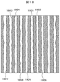
- FIG. 18 shows an observation image obtained in this example.
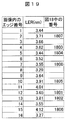
- FIG. 19 is an example of a diagram in which a table obtained as a result of the present embodiment is displayed on the operation terminal screen.
- Fig. 17 shows a schematic diagram of the pattern formation process.
- FIG. 17 is a schematic cross-sectional view of a pattern for explaining a process of forming fine lines and spaces using SADP three times.
- 17 (a) to 17 (c) show the process of forming a line pattern by the first SADP
- FIGS. 17 (d) to 17 (e) form the line pattern by the second SADP.
- Steps, FIGS. 17 (f) to 17 (g) show a step of forming a line pattern by the third SADP.
- the silicon oxide film 228, the carbon film 227, the silicon oxide film 226, the silicon nitride film 225, the silicon oxide film 224, the carbon film 223, and the antireflection film 222 which are sequentially stacked from the bottom, are patterned in a line shape.
- a resist layer 221 is formed (FIG. 17A). Note that although there is only one resist layer 121 in the drawing, a large number of resist layers are actually formed.
- a silicon oxide film 231 is formed so as to cover the resist layer 221, and the silicon oxide film 131 is anisotropically etched to form line-shaped silicon oxide films 231 on both sides of the resist layer 221.
- the layer 221 is removed by ashing or the like (FIG. 1B).
- the line-shaped silicon oxide film 231 is formed by etching anisotropically etching the laminated film of the antireflection film 222 and the carbon film 223 (FIG. 1C). Thereby, it is possible to form a dense pattern having a pitch that is half the pitch of the pattern created by the first lithography.
- the silicon oxide film 241 is etched by anisotropic dry etching so that both sides of the carbon film 223 are formed. A line-shaped silicon oxide film 241 is formed, and the carbon film 223 is removed (FIG. 17D).
- anisotropic etching is performed using the silicon oxide film 241 as a mask, thereby forming a laminated film of the line-shaped silicon oxide film 224 and the silicon nitride film 225 (FIG. 17E). Thereby, the pitch can be further divided with respect to the pattern formed by SADP.
- the silicon oxide film 224 is removed, the silicon oxide film 251 is formed so as to cover the line-shaped silicon nitride film 225, and then the silicon oxide film 251 is etched by anisotropic dry etching.
- a line-shaped silicon oxide film 251 is formed on the side, and the silicon nitride film 225 is removed (FIG. 17F).
- anisotropic etching is performed using the silicon oxide film 251 as a mask to form a laminated film of the line-shaped silicon oxide film 226 and the carbon film 227 (FIG. 17G).
- the pitch can be further divided with respect to the pattern formed by SAQP.
- the said material is an example and is not limited to the said material.
- FIG. 18 shows a schematic diagram of an image obtained by observing the fine line & space pattern produced in the process shown in FIG.
- the diagonal lattice pattern part is a space
- the white part is a line pattern.
- the shapes of the edges belonging to the line group 1701 are all similar, and the shapes of the edges belonging to the line group 1702 are all similar. Accordingly, by examining the distribution of the similarity between adjacent edges, the candidate position of the initial core and the candidate position of the gap are determined.
- the initial core is between the line group 1701 and the line group 1702, but the left side of the line group 1701 or the right side of the line group 1702 (these are gaps) in the figure cannot be distinguished at this stage.
- the initial core is between the twelfth edge 1801 and the thirteenth edge 1802 from the left and between the fourth edge 1803 and the fifth edge 1804 from the left in the image. It turned out to be a candidate.
- the outer edges of one space outside the initial core in FIG. 17, that is, the edges 1703 and 1704 have the largest LER. Further, the edges adjacent to the gap, that is, the edges 1705 and 1706 and the edge 1707 have the smallest LER. Therefore, assuming that the initial core is between the edge 1801 and the edge 1802, the left edge (the tenth from the left) 1805 of the left space with respect to the line including the edge 1801 where the LER is expected to be large, The right edge (15th from the left) 1806 of the right space with respect to the line including the edge 1802, and the LER of the edge 1803 and the edge 1804 assumed to have a small LER were calculated.
- Fig. 19 shows an example of a diagram in which the result is displayed on the operation terminal screen.
- the LERs of the edges 1805 and 1806 are large and the LERs of the edges 1803 and 1804 are relatively small.
- the LERs of the edges 1807 and 1808 and the LERs of the edges 1801 and 1802 are compared, but these values are almost the same and no difference is observed.
- the former was estimated to be correct, and the initial core was determined to be between the edge 1801 and the edge 1802.
- this invention is not limited to the above-mentioned Example, Various modifications are included.
- the above-described embodiments have been described in detail for easy understanding of the present invention, and are not necessarily limited to those having all the configurations described.
- a part of the configuration of a certain embodiment can be replaced with the configuration of another embodiment, and the configuration of another embodiment can be added to the configuration of a certain embodiment.
- the position of the line pattern A line edge roughness value is calculated from a group of adjacent lines, and the line edge roughness value is calculated. From the distribution of the line edge roughness value in the image, the line or space where the center of the first pattern is located is calculated.
- a pattern inspection method characterized by identifying whether or not the pattern is formed at a position.
- the position of the line pattern that was formed before the last film deposition is determined by calculating the similarity of the shape of the center variation of adjacent lines as the variation,
- a line edge roughness value is calculated from a group of adjacent lines, and the line edge roughness value is calculated. From the distribution of the line edge roughness value in the image, the line or space where the center of the first pattern is located is calculated.
- a pattern inspection method characterized by identifying whether or not the pattern is formed at a position.
- a pattern inspection apparatus for observing a sample having a line pattern from above, An arithmetic unit for extracting pattern edges from an image; At least an arithmetic unit that calculates the similarity between the shapes of two adjacent edges across a space or an arithmetic unit that calculates the degree of similarity in a direction along the center line of two adjacent lines across a space
- An analysis device for analyzing the distribution of line edge roughness values; A device for storing image and edge position data;
- a pattern inspection apparatus comprising:
- antireflection film 223 ... carbon film, 224 ... silicon oxide film, 225 ... silicon nitride Film, 226... Silicon oxide film, 227... Carbon film, 228.
Landscapes
- Chemical & Material Sciences (AREA)
- Analytical Chemistry (AREA)
- Physics & Mathematics (AREA)
- General Physics & Mathematics (AREA)
- Engineering & Computer Science (AREA)
- Health & Medical Sciences (AREA)
- Environmental & Geological Engineering (AREA)
- Epidemiology (AREA)
- Public Health (AREA)
- Length-Measuring Devices Using Wave Or Particle Radiation (AREA)
- Testing Or Measuring Of Semiconductors Or The Like (AREA)
- Manufacturing & Machinery (AREA)
Abstract
Description
積層膜上に形成されたライン状の第一パターンを覆い、膜堆積を行って第一パターンの両側壁にライン状の第二パターンを形成する工程を2回以上行うことで形成される複数のライン状パターンを有する試料を載置する試料台と、
前記荷電粒子源から放出された荷電粒子を荷電粒子線として前記試料台に載置された前記試料へ照射する照射光学系と、
前記荷電粒子線の照射により前記試料から放出された二次荷電粒子を検出する検出器と、
前記検出器により検出された前記二次荷電粒子の信号に基づいて得られる前記試料の表面の画像データを表示する表示部と、
前記画像データに基づき、前記試料において隣接して並ぶ複数のライン状パターンのラインエッジの凹凸の指標であるラインエッジラフネス値を算出する算出部と、
前記複数のライン状パターンにおける前記ラインエッジラフネス値同士を比較し、前記第一パターンの中心であるイニシャルコアの位置を判定する判定部と、を有することを特徴とする荷電粒子線装置とする。
前記試料は、積層膜上に形成されたライン状の第一パターンを覆い、膜堆積を行って第一パターンの両側壁にライン状の第二パターンを形成する工程を2回以上行うことで形成される複数のライン状パターンを有する試料を載置する試料台と、
前記荷電粒子源から放出された荷電粒子を荷電粒子線として前記試料台に載置された前記試料へ照射する照射光学系と、
前記荷電粒子線の照射により前記試料から放出された二次荷電粒子を検出する検出器と、
前記検出器により検出された前記二次荷電粒子の信号に基づいて得られる前記試料の表面の画像データを表示する表示部と、
前記画像データに基づき、前記試料において隣接して並ぶ複数のスペースの左右のエッジ形状の類似度を算出する算出部と、
前記ライン状のパターンまたは前記スペースにおける左右のエッジ形状の類似度に基づき、前記第一パターンの両側に形成された前記第二パターンであるセカンドコアの位置を判定する判定部と、を有することを特徴とする荷電粒子線装置とする。
積層膜上に形成されたライン状の第一パターンを覆い、膜堆積を行って第一パターンの両側壁にライン状の第二パターンを形成する工程を2回以上行うことで形成される複数のライン状パターンを有する試料を載置する試料台と、
前記荷電粒子源から放出された荷電粒子を荷電粒子線として前記試料台に載置された前記試料に照射する照射光学系と、
前記荷電粒子線の照射により前記試料から放出された二次荷電粒子を検出する検出器と、
前記検出器により検出された前記二次荷電粒子の信号に基づいて得られる前記試料の表面の画像データを表示する表示部と、
前記複数のライン状パターンのスペースを挟んで隣接するエッジの凹凸形状の類似度或いは隣接して並ぶ前記複数のライン状パターンに対してライン中心位置のライン長手方向に沿った変動を算出することによりラインの中心変動として隣接するラインの中心変動の形状の類似度を算出する類似度算出部と、
前記エッジの凹凸形状の類似度または前記ラインの中心変動の形状の類似度に基づき、最後の膜堆積の前に形成されたライン状パターンの位置を判定する位置判定部と、
隣接して並ぶ前記複数のライン状パターンのラインエッジの凹凸の指標であるラインエッジラフネス値を算出する、ラフネス値算出部と、
前記最後の膜堆積の前に形成されたライン状パターンの位置および前記ラインエッジラフネス値に基づき、前記第一パターンの中心であるイニシャルコアの位置を判定するイニシャルコア判定部と、を有することを特徴とする荷電粒子線装置とする。
前記画像データに基づき、前記試料において隣接して並ぶ複数のライン状パターンのラインエッジの凹凸の指標であるラインエッジラフネス値を算出する算出部と、
前記複数のライン状パターンにおける前記ラインエッジラフネス値同士を比較し、前記第一パターンの中心であるイニシャルコアの位置を判定する判定部と、
を有することを特徴とする検査装置とする。
前記ライン状のパターンまたは前記スペースにおける左右のエッジ形状の類似度に基づき、前記第一パターンの両側に形成された前記第二パターンであるセカンドコアの位置を判定する判定部と、
を有することを特徴とする検査装置とする。
前記複数のライン状パターンのスペースを挟んで隣接するエッジの凹凸形状の類似度或いは隣接して並ぶ前記複数のライン状パターンに対してライン中心位置のライン長手方向に沿った変動を算出することによりラインの中心変動として隣接するラインの中心変動の形状の類似度を算出する類似度算出部と、
前記エッジの凹凸形状の類似度または前記ラインの中心変動の形状の類似度に基づき、最後の膜堆積の前に形成されたライン状パターンの位置を判定する位置判定部と、
隣接して並ぶ前記複数のライン状パターンのラインエッジの凹凸の指標であるラインエッジラフネス値を算出する、ラフネス値算出部と、
前記最後の膜堆積の前に形成されたライン状パターンの位置および前記ラインエッジラフネス値に基づき、前記第一パターンの中心であるイニシャルコアの位置を判定するイニシャルコア判定部と、有することを特徴とする検査装置とする。






本手法の前提となる膜堆積によるライン形成時のエッジ形状の転写について説明する。図5(a)は、コアパターンに対して膜を堆積したのち、エッチングを行ってコア部分を露出させ、さらにコアを除去して得られるラインパターンのエッジのトップビューの模式図であり、図5(b)は、コアパターンに対して膜を堆積したときの断面の模式図である。図5(a)と(b)とで同じ番号を用いているエッジは対応している。図5(a)では破線で示されている符号501は堆積した膜の表面に相当するラインエッジであり、実線で示されている符号502はコアパターンのラインエッジである。
同様に、重要な寸法指標として、スペースパターンの幅がある。この値の周期的な変化は主として1回目の製膜工程での膜の不均一性による。このような不均一性が発現する原因は、上記のCDL_finalの場合と同じである。この指標自体は従来計測されてきたスペース幅と同じものであるが、イニシャルコアの位置がわかれば、区別することができる。イニシャルコアのスペース幅をCDS_initcore、セカンドコアのスペース幅をCDS_2ndcore、ギャップのスペース幅をCDS_gapとし、それらの値を比較すれば、工程の影響を分離できる。複数のデータがある場合は、平均値をとるとよい。例えば、CDS_2ndcoreが異常に小さい値であれば、1回目の製膜で膜堆積量が不十分だったということになる(詳細は実施例に記す)。
以下、本発明を実施例により詳細に説明する。
(1)基板上に形成された第一のパターンに対して膜堆積を行って第一のパターンの両側壁に第二のパターンを形成するという工程を1回以上行うことで形成される複数のラインパターンを有する試料に対して、上空から観察を行うパターン検査方法であって、隣接して並ぶ複数のライン群からそれぞれのラインエッジの凹凸の指標即ちラインエッジラフネス値を算出し、ラインエッジラフネス値の画像内における分布から、第一のパターンの中心がどこのラインまたはスペースの位置に形成されていたかを特定することを特徴とするパターン検査方法。
(2)基板上に形成された第一のパターンに対して膜堆積を行って第一のパターンの両側壁に第二のパターンを形成するという工程を1回以上行うことで形成される複数のラインパターンを有する試料に対して、上空から観察を行うパターン検査方法であって、スペースを挟んで隣接するエッジの凹凸形状の類似度を算出することで、最後の膜堆積の前に形成されていたラインパターンの位置を特定し、
隣接して並ぶ複数のライン群からそれぞれのラインエッジの凹凸の指標即ちラインエッジラフネス値を算出し、ラインエッジラフネス値の画像内における分布から、第一のパターンの中心がどこのラインまたはスペースの位置に形成されていたかを特定することを特徴とするパターン検査方法。
(3)基板上に形成された第一のパターンに対して膜堆積を行って第一のパターンの両側壁に第二のパターンを形成するという工程を1回以上行うことで形成される複数のラインパターンを有する試料に対して、上空から観察を行うパターン検査方法であって、隣接して並ぶ複数のラインに対してライン中心位置のライン長手方向に沿った変動を算出しそれをラインの中心変動とし、隣接するラインの中心変動の形の類似度を算出することで、最後の膜堆積の前に形成されていたラインパターンの位置を特定し、
隣接して並ぶ複数のライン群からそれぞれのラインエッジの凹凸の指標即ちラインエッジラフネス値を算出し、ラインエッジラフネス値の画像内における分布から、第一のパターンの中心がどこのラインまたはスペースの位置に形成されていたかを特定することを特徴とするパターン検査方法。
(4)(1)乃至(3)の何れかに記載のパターン検査方法であって、第一のパターンのエッジの位置に形成されているエッジと、第一のパターンから最も遠い位置に形成されているエッジについてのラインエッジラフネス値のみを用いることを特徴とするパターン検査方法。
(5)(1)乃至4の何れかに記載のパターン検査方法であって、画像内において特定された第一のパターンの中心があった位置を基準として、予め定められた位置にある二つのエッジの距離を算出することを特徴とするパターン検査方法。
(6)基板上に形成された第一のパターンに対して膜堆積を行って第一のパターンの両側壁に第二のパターンを形成するという工程を1回以上行うことで形成される複数のラインパターンを有する試料に対して、上空から観察を行うパターン検査装置であって、
画像からパターンのエッジを抽出するための演算装置と、
スペースを挟んで隣接する二つのエッジの形状の類似度を算出する演算装置かスペースを挟んで隣接する二つのラインの中央位置のラインに沿った方向の変動の類似度を算出する演算装置の少なくとも一方と、
ラインエッジラフネスの値の分布を解析する解析装置と、
画像及びエッジ位置のデータとを記憶するための装置と、
を備えたことを特徴とするパターン検査装置。
Claims (15)
- 荷電粒子源と、
積層膜上に形成されたライン状の第一パターンを覆い、膜堆積を行って第一パターンの両側壁にライン状の第二パターンを形成する工程を2回以上行うことで形成される複数のライン状パターンを有する試料を載置する試料台と、
前記荷電粒子源から放出された荷電粒子を荷電粒子線として前記試料台に載置された前記試料へ照射する照射光学系と、
前記荷電粒子線の照射により前記試料から放出された二次荷電粒子を検出する検出器と、
前記検出器により検出された前記二次荷電粒子の信号に基づいて得られる前記試料の表面の画像データを表示する表示部と、 前記画像データに基づき、前記試料において隣接して並ぶ複数のライン状パターンのラインエッジの凹凸の指標であるラインエッジラフネス値を算出する算出部と、
前記複数のライン状パターンにおける前記ラインエッジラフネス値同士を比較し、前記第一パターンの中心であるイニシャルコアの位置を判定する判定部と、を有することを特徴とする荷電粒子線装置。 - 請求項1記載の荷電粒子線装置において、
前記試料は、前記第一パターンに対して2本の前記第二パターンが形成され、更に、前記第二パターンに対してそれぞれ2本ずつ形成された合計4本のライン状パターンを有し、
前記判定部は、前記4本のラインにおける前記ラインエッジラフネス値の大きさを比較したとき、順に小中大中中大中小であった場合、前記イニシャルコアはラインエッジラフネス値が中中となるラインエッジで挟まれた位置にあることを判定することを特徴とする荷電粒子線装置。 - 請求項1記載の荷電粒子線装置において、
前記判定部は、前記ライン状パターンがポジ型プロセスで形成された場合、前記イニシャルコアがスペース部に位置すると判定することを特徴とする荷電粒子線装置。 - 請求項1記載の荷電粒子線装置において、
前記判定部は、前記ライン状パターンがネガ型プロセスで形成された場合、前記イニシャルコアがライン部に位置すると判定することを特徴とする荷電粒子線装置。 - 請求項1記載の荷電粒子線装置において、
前記イニシャルコアの位置を基準として、予め定められた位置にある二つのエッジの距離を算出するエッジ算出部を有することを特徴とする荷電粒子線装置。 - 請求項1記載の荷電粒子線装置において、
前記表示部は、前記第一パターンの幅、或いは前記イニシャルコアの幅と前記イニシャルコアを挟んで両側に配置されるライン或いはスペースの幅を合計した値を表示することを特徴とする荷電粒子線装置。 - 荷電粒子源と、
前記試料は、積層膜上に形成されたライン状の第一パターンを覆い、膜堆積を行って第一パターンの両側壁にライン状の第二パターンを形成する工程を2回以上行うことで形成される複数のライン状パターンを有する試料を載置する試料台と、
前記荷電粒子源から放出された荷電粒子を荷電粒子線として前記試料台に載置された前記試料へ照射する照射光学系と、
前記荷電粒子線の照射により前記試料から放出された二次荷電粒子を検出する検出器と、
前記検出器により検出された前記二次荷電粒子の信号に基づいて得られる前記試料の表面の画像データを表示する表示部と、 前記画像データに基づき、前記試料において隣接して並ぶ複数のスペースの左右のエッジ形状の類似度を算出する算出部と、
前記ライン状のパターンまたは前記スペースにおける左右のエッジ形状の類似度に基づき、前記第一パターンの両側に形成された前記第二パターンであるセカンドコアの位置を判定する判定部と、を有することを特徴とする荷電粒子線装置。 - 請求項7記載の荷電粒子線装置において、
前記判定部は、
前記セカンドコアの位置に基づいて、前記第一パターンの中心であるイニシャルコアの位置を判定することを特徴とする荷電粒子線装置。 - 請求項8記載の荷電粒子線装置において、
前記画像データに基づき、前記試料において隣接して並ぶ複数のライン状パターンのラインエッジの凹凸の指標であるラインエッジラフネス値を算出する算出部を有し、
前記判定部は、前記複数のライン状パターンにおける前記ラインエッジラフネス値同士を比較し、前記比較した結果と、前記複数のライン状パターンにおいて実測された前記ラインエッジラフネス値との相関値を求め、前記イニシャルコアの位置を判定することを特徴とする荷電粒子線装置。 - 請求項9記載の荷電粒子線装置において、
前記表示部は、前記イニシャルコアの位置と前記相関値とを表示することを特徴とする荷電粒子線装置。 - 荷電粒子源と、
積層膜上に形成されたライン状の第一パターンを覆い、膜堆積を行って第一パターンの両側壁にライン状の第二パターンを形成する工程を2回以上行うことで形成される複数のライン状パターンを有する試料を載置する試料台と、
前記荷電粒子源から放出された荷電粒子を荷電粒子線として前記試料台に載置された前記試料に照射する照射光学系と、
前記荷電粒子線の照射により前記試料から放出された二次荷電粒子を検出する検出器と、
前記検出器により検出された前記二次荷電粒子の信号に基づいて得られる前記試料の表面の画像データを表示する表示部と、 前記複数のライン状パターンのスペースを挟んで隣接するエッジの凹凸形状の類似度或いは隣接して並ぶ前記複数のライン状パターンに対してライン中心位置のライン長手方向に沿った変動を算出することによりラインの中心変動として隣接するラインの中心変動の形状の類似度を算出する類似度算出部と、
前記エッジの凹凸形状の類似度または前記ラインの中心変動の形状の類似度に基づき、最後の膜堆積の前に形成されたライン状パターンの位置を判定する位置判定部と、
隣接して並ぶ前記複数のライン状パターンのラインエッジの凹凸の指標であるラインエッジラフネス値を算出する、ラフネス値算出部と、
前記最後の膜堆積の前に形成されたライン状パターンの位置および前記ラインエッジラフネス値に基づき、前記第一パターンの中心であるイニシャルコアの位置を判定するイニシャルコア判定部と、を有することを特徴とする荷電粒子線装置。 - 積層膜上に形成されたライン状の第一パターンを覆い、膜堆積を行って第一パターンの両側壁にライン状の第二パターンを形成する工程を2回以上行うことで形成される複数のライン状パターンを有する試料へ荷電粒子線を照射し得られる前記試料の表面の画像データを表示する表示部と、
前記画像データに基づき、前記試料において隣接して並ぶ複数のライン状パターンのラインエッジの凹凸の指標であるラインエッジラフネス値を算出する算出部と、
前記複数のライン状パターンにおける前記ラインエッジラフネス値同士を比較し、前記第一パターンの中心であるイニシャルコアの位置を判定する判定部と、
を有することを特徴とする検査装置。 - 積層膜上に形成されたライン状の第一パターンを覆い、膜堆積を行って第一パターンの両側壁にライン状の第二パターンを形成する工程を2回以上行うことで形成される複数のライン状パターンを有する試料へ荷電粒子線を照射し得られる前記試料の表面の画像データを表示する表示部と、
前記画像データに基づき、前記試料において隣接して並ぶ複数のスペースの左右のエッジ形状の類似度を算出する算出部と、
前記ライン状のパターンまたは前記スペースにおける左右のエッジ形状の類似度に基づき、前記第一パターンの両側に形成された前記第二パターンであるセカンドコアの位置を判定する判定部と、
を有することを特徴とする検査装置。 - 積層膜上に形成されたライン状の第一パターンを覆い、膜堆積を行って第一パターンの両側壁にライン状の第二パターンを形成する工程を2回以上行うことで形成される複数のライン状パターンを有する試料へ荷電粒子線を照射し得られる前記試料の表面の画像データを表示する表示部と、
前記複数のライン状パターンのスペースを挟んで隣接するエッジの凹凸形状の類似度或いは隣接して並ぶ前記複数のライン状パターンに対してライン中心位置のライン長手方向に沿った変動を算出することによりラインの中心変動として隣接するラインの中心変動の形状の類似度を算出する類似度算出部と、
前記エッジの凹凸形状の類似度または前記ラインの中心変動の形状の類似度に基づき、最後の膜堆積の前に形成されたライン状パターンの位置を判定する位置判定部と、
隣接して並ぶ前記複数のライン状パターンのラインエッジの凹凸の指標であるラインエッジラフネス値を算出する、ラフネス値算出部と、
前記最後の膜堆積の前に形成されたライン状パターンの位置および前記ラインエッジラフネス値に基づき、前記第一パターンの中心であるイニシャルコアの位置を判定するイニシャルコア判定部と、有することを特徴とする検査装置。 - 請求項12乃至14に記載の検査装置において、
前記ライン状パターンまたは前記ライン状パターンのスペースの幅を算出することを特徴とする検査装置。
Priority Applications (2)
| Application Number | Priority Date | Filing Date | Title |
|---|---|---|---|
| US15/303,813 US9824938B2 (en) | 2014-04-14 | 2015-03-31 | Charged particle beam device and inspection device |
| KR1020167027412A KR101842055B1 (ko) | 2014-04-14 | 2015-03-31 | 하전 입자선 장치 및 검사 장치 |
Applications Claiming Priority (2)
| Application Number | Priority Date | Filing Date | Title |
|---|---|---|---|
| JP2014-082640 | 2014-04-14 | ||
| JP2014082640A JP6227466B2 (ja) | 2014-04-14 | 2014-04-14 | 荷電粒子線装置および検査装置 |
Publications (1)
| Publication Number | Publication Date |
|---|---|
| WO2015159705A1 true WO2015159705A1 (ja) | 2015-10-22 |
Family
ID=54323916
Family Applications (1)
| Application Number | Title | Priority Date | Filing Date |
|---|---|---|---|
| PCT/JP2015/060205 Ceased WO2015159705A1 (ja) | 2014-04-14 | 2015-03-31 | 荷電粒子線装置および検査装置 |
Country Status (5)
| Country | Link |
|---|---|
| US (1) | US9824938B2 (ja) |
| JP (1) | JP6227466B2 (ja) |
| KR (1) | KR101842055B1 (ja) |
| TW (1) | TWI529369B (ja) |
| WO (1) | WO2015159705A1 (ja) |
Families Citing this family (26)
| Publication number | Priority date | Publication date | Assignee | Title |
|---|---|---|---|---|
| US10559501B2 (en) * | 2016-09-20 | 2020-02-11 | Qualcomm Incorporated | Self-aligned quadruple patterning process for Fin pitch below 20nm |
| KR102309432B1 (ko) | 2017-01-27 | 2021-10-05 | 주식회사 히타치하이테크 | 하전 입자선 장치 |
| US10901325B2 (en) * | 2017-02-28 | 2021-01-26 | Kla-Tencor Corporation | Determining the impacts of stochastic behavior on overlay metrology data |
| US10622266B2 (en) * | 2017-04-04 | 2020-04-14 | Globalfoundries Inc. | Methods of identifying space within integrated circuit structure as mandrel space or non-mandrel space |
| US10488188B2 (en) | 2017-04-13 | 2019-11-26 | Fractilia, Llc | System and method for removing noise from roughness measurements |
| US10664955B2 (en) | 2017-04-13 | 2020-05-26 | Fractilia, Llc | Edge detection system and its use for machine learning |
| US10176966B1 (en) | 2017-04-13 | 2019-01-08 | Fractilia, Llc | Edge detection system |
| US11380516B2 (en) | 2017-04-13 | 2022-07-05 | Fractilia, Llc | System and method for generating and analyzing roughness measurements and their use for process monitoring and control |
| US12142454B2 (en) | 2017-04-13 | 2024-11-12 | Fractilla, LLC | Detection of probabilistic process windows |
| US10648801B2 (en) | 2017-04-13 | 2020-05-12 | Fractilia, Llc | System and method for generating and analyzing roughness measurements and their use for process monitoring and control |
| US11508546B2 (en) | 2017-04-13 | 2022-11-22 | Fractilia, Llc | System and method for low-noise edge detection and its use for process monitoring and control |
| US11521825B2 (en) | 2017-04-13 | 2022-12-06 | Fractilia, Llc | System and method for predicting stochastic-aware process window and yield and their use for process monitoring and control |
| US11355306B2 (en) | 2017-04-13 | 2022-06-07 | Fractilia, Llc | System and method for generating and analyzing roughness measurements and their use for process monitoring and control |
| US10522322B2 (en) | 2017-04-13 | 2019-12-31 | Fractilia, Llc | System and method for generating and analyzing roughness measurements |
| US11361937B2 (en) | 2017-04-13 | 2022-06-14 | Fractilia, Llc | System and method for generating and analyzing roughness measurements and their use for process monitoring and control |
| US10656532B2 (en) | 2017-04-13 | 2020-05-19 | Fractilia, Llc | Edge detection system and its use for optical proximity correction |
| US10727045B2 (en) | 2017-09-29 | 2020-07-28 | Taiwan Semiconductor Manufacturing Company, Ltd. | Method for manufacturing a semiconductor device |
| US10473460B2 (en) * | 2017-12-11 | 2019-11-12 | Kla-Tencor Corporation | Overlay measurements of overlapping target structures based on symmetry of scanning electron beam signals |
| US11398379B2 (en) | 2018-03-20 | 2022-07-26 | Tokyo Electron Limited | Platform and method of operating for integrated end-to-end self-aligned multi-patterning process |
| CN111381436B (zh) * | 2018-12-27 | 2024-03-08 | 中芯国际集成电路制造(上海)有限公司 | 具有图形的光罩的制造方法 |
| US12354829B2 (en) * | 2019-08-23 | 2025-07-08 | Hitachi High-Tech Corporation | Overlay measurement system and overlay measurement device for overlay error measurement using electron microscopy |
| EP3862814A1 (en) * | 2020-02-10 | 2021-08-11 | ASML Netherlands B.V. | Multi-step process inspection method |
| KR102690867B1 (ko) * | 2020-02-20 | 2024-08-05 | 주식회사 히타치하이테크 | 패턴 매칭 장치, 패턴 측정 시스템 및 비일시적 컴퓨터 가독 매체 |
| US11443825B2 (en) | 2020-12-02 | 2022-09-13 | Winbond Electronics Corp. | Failure mode analysis method for memory device |
| JP7555896B2 (ja) * | 2021-09-30 | 2024-09-25 | 株式会社日立ハイテク | 荷電粒子線画像処理装置とそれを備える荷電粒子線装置 |
| KR20250034980A (ko) * | 2022-09-08 | 2025-03-11 | 주식회사 히타치하이테크 | 치수 계측 시스템, 추정 시스템 및 치수 계측 방법 |
Citations (2)
| Publication number | Priority date | Publication date | Assignee | Title |
|---|---|---|---|---|
| JP2011133378A (ja) * | 2009-12-25 | 2011-07-07 | Hitachi High-Technologies Corp | パターン測定装置 |
| US20140083972A1 (en) * | 2012-09-27 | 2014-03-27 | Tokyo Electron Limited | Pattern forming method |
Family Cites Families (2)
| Publication number | Priority date | Publication date | Assignee | Title |
|---|---|---|---|---|
| JP5543984B2 (ja) * | 2009-03-02 | 2014-07-09 | アプライド マテリアルズ イスラエル リミテッド | 類似構造要素を分類するcd計測システム及び方法 |
| JP5426497B2 (ja) | 2010-08-09 | 2014-02-26 | 株式会社アドバンテスト | パターン測定装置及びパターン測定方法 |
-
2014
- 2014-04-14 JP JP2014082640A patent/JP6227466B2/ja not_active Expired - Fee Related
-
2015
- 2015-03-31 US US15/303,813 patent/US9824938B2/en not_active Expired - Fee Related
- 2015-03-31 KR KR1020167027412A patent/KR101842055B1/ko active Active
- 2015-03-31 WO PCT/JP2015/060205 patent/WO2015159705A1/ja not_active Ceased
- 2015-04-14 TW TW104111939A patent/TWI529369B/zh not_active IP Right Cessation
Patent Citations (2)
| Publication number | Priority date | Publication date | Assignee | Title |
|---|---|---|---|---|
| JP2011133378A (ja) * | 2009-12-25 | 2011-07-07 | Hitachi High-Technologies Corp | パターン測定装置 |
| US20140083972A1 (en) * | 2012-09-27 | 2014-03-27 | Tokyo Electron Limited | Pattern forming method |
Also Published As
| Publication number | Publication date |
|---|---|
| TWI529369B (zh) | 2016-04-11 |
| TW201538928A (zh) | 2015-10-16 |
| US20170040230A1 (en) | 2017-02-09 |
| JP2015203614A (ja) | 2015-11-16 |
| US9824938B2 (en) | 2017-11-21 |
| JP6227466B2 (ja) | 2017-11-08 |
| KR101842055B1 (ko) | 2018-03-27 |
| KR20160132048A (ko) | 2016-11-16 |
Similar Documents
| Publication | Publication Date | Title |
|---|---|---|
| JP6227466B2 (ja) | 荷電粒子線装置および検査装置 | |
| TWI755386B (zh) | 計量系統及方法 | |
| JP5543984B2 (ja) | 類似構造要素を分類するcd計測システム及び方法 | |
| TWI517210B (zh) | Pattern evaluation method and pattern evaluation device | |
| JP4364524B2 (ja) | パターン検査方法 | |
| CN104919307B (zh) | 图案评价装置以及具备图案评价装置的外观检查装置 | |
| US9000365B2 (en) | Pattern measuring apparatus and computer program | |
| JP7219334B2 (ja) | 3d-nand cdsem計測学のための方法、システムおよびコンピュータプログラム製品 | |
| JP2006215020A5 (ja) | ||
| CN111566789A (zh) | 使用电子显微法的半导体计量及缺陷分类 | |
| JP6129651B2 (ja) | ラインパターンの形状評価方法及びその装置 | |
| WO2011001635A1 (ja) | 半導体検査装置及びそれを用いた半導体検査方法 | |
| CN114365183A (zh) | 晶片检验方法和系统 | |
| TWI823460B (zh) | 計測方法、計測系統、及非暫態性電腦可讀媒體 | |
| CN110582842A (zh) | 依据光学检验结果进行计量导引检验样品成形 | |
| KR101328611B1 (ko) | 반도체 메모리 디바이스 제조를 위한 패턴 매칭 방법 | |
| CN115760675A (zh) | 半导体样本中的局部形状偏差 | |
| WO2018042600A1 (ja) | 画像解析装置および荷電粒子線装置 | |
| Sezestre et al. | Model-based contour extraction: an enabler for very low-frame SEM images metrology | |
| KR20190088761A (ko) | 웨이퍼 측정 설비, 웨이퍼 측정 시스템 및 이를 이용한 반도체 장치의 제조 방법 | |
| US20250306474A1 (en) | Semiconductor Pattern Evaluation Method, Semiconductor Manufacturing Process Management System, and Semiconductor Pattern Evaluation System | |
| CN115380207B (zh) | 图案匹配方法 | |
| US20110224934A1 (en) | Evaluating apparatus, evaluating method, and computer program product | |
| US20190243927A1 (en) | Verifying planarization performance using electrical measures |
Legal Events
| Date | Code | Title | Description |
|---|---|---|---|
| 121 | Ep: the epo has been informed by wipo that ep was designated in this application |
Ref document number: 15780146 Country of ref document: EP Kind code of ref document: A1 |
|
| ENP | Entry into the national phase |
Ref document number: 20167027412 Country of ref document: KR Kind code of ref document: A |
|
| WWE | Wipo information: entry into national phase |
Ref document number: 15303813 Country of ref document: US |
|
| NENP | Non-entry into the national phase |
Ref country code: DE |
|
| 122 | Ep: pct application non-entry in european phase |
Ref document number: 15780146 Country of ref document: EP Kind code of ref document: A1 |