WO2015156231A1 - Metamaterial optical member, light detection device, laser excitation light source, and measuring device - Google Patents
Metamaterial optical member, light detection device, laser excitation light source, and measuring device Download PDFInfo
- Publication number
- WO2015156231A1 WO2015156231A1 PCT/JP2015/060651 JP2015060651W WO2015156231A1 WO 2015156231 A1 WO2015156231 A1 WO 2015156231A1 JP 2015060651 W JP2015060651 W JP 2015060651W WO 2015156231 A1 WO2015156231 A1 WO 2015156231A1
- Authority
- WO
- WIPO (PCT)
- Prior art keywords
- light
- optical member
- metamaterial
- incident
- metamaterial optical
- Prior art date
Links
Images


Classifications
-
- G—PHYSICS
- G02—OPTICS
- G02B—OPTICAL ELEMENTS, SYSTEMS OR APPARATUS
- G02B1/00—Optical elements characterised by the material of which they are made; Optical coatings for optical elements
- G02B1/10—Optical coatings produced by application to, or surface treatment of, optical elements
- G02B1/11—Anti-reflection coatings
-
- G—PHYSICS
- G01—MEASURING; TESTING
- G01N—INVESTIGATING OR ANALYSING MATERIALS BY DETERMINING THEIR CHEMICAL OR PHYSICAL PROPERTIES
- G01N21/00—Investigating or analysing materials by the use of optical means, i.e. using sub-millimetre waves, infrared, visible or ultraviolet light
- G01N21/17—Systems in which incident light is modified in accordance with the properties of the material investigated
- G01N21/25—Colour; Spectral properties, i.e. comparison of effect of material on the light at two or more different wavelengths or wavelength bands
- G01N21/255—Details, e.g. use of specially adapted sources, lighting or optical systems
-
- G—PHYSICS
- G01—MEASURING; TESTING
- G01N—INVESTIGATING OR ANALYSING MATERIALS BY DETERMINING THEIR CHEMICAL OR PHYSICAL PROPERTIES
- G01N21/00—Investigating or analysing materials by the use of optical means, i.e. using sub-millimetre waves, infrared, visible or ultraviolet light
- G01N21/01—Arrangements or apparatus for facilitating the optical investigation
- G01N21/03—Cuvette constructions
- G01N21/0303—Optical path conditioning in cuvettes, e.g. windows; adapted optical elements or systems; path modifying or adjustment
-
- G—PHYSICS
- G01—MEASURING; TESTING
- G01N—INVESTIGATING OR ANALYSING MATERIALS BY DETERMINING THEIR CHEMICAL OR PHYSICAL PROPERTIES
- G01N21/00—Investigating or analysing materials by the use of optical means, i.e. using sub-millimetre waves, infrared, visible or ultraviolet light
- G01N21/01—Arrangements or apparatus for facilitating the optical investigation
- G01N21/03—Cuvette constructions
- G01N21/05—Flow-through cuvettes
-
- G—PHYSICS
- G01—MEASURING; TESTING
- G01N—INVESTIGATING OR ANALYSING MATERIALS BY DETERMINING THEIR CHEMICAL OR PHYSICAL PROPERTIES
- G01N21/00—Investigating or analysing materials by the use of optical means, i.e. using sub-millimetre waves, infrared, visible or ultraviolet light
- G01N21/17—Systems in which incident light is modified in accordance with the properties of the material investigated
- G01N21/25—Colour; Spectral properties, i.e. comparison of effect of material on the light at two or more different wavelengths or wavelength bands
- G01N21/27—Colour; Spectral properties, i.e. comparison of effect of material on the light at two or more different wavelengths or wavelength bands using photo-electric detection ; circuits for computing concentration
-
- G—PHYSICS
- G01—MEASURING; TESTING
- G01N—INVESTIGATING OR ANALYSING MATERIALS BY DETERMINING THEIR CHEMICAL OR PHYSICAL PROPERTIES
- G01N21/00—Investigating or analysing materials by the use of optical means, i.e. using sub-millimetre waves, infrared, visible or ultraviolet light
- G01N21/17—Systems in which incident light is modified in accordance with the properties of the material investigated
- G01N21/59—Transmissivity
-
- G—PHYSICS
- G01—MEASURING; TESTING
- G01N—INVESTIGATING OR ANALYSING MATERIALS BY DETERMINING THEIR CHEMICAL OR PHYSICAL PROPERTIES
- G01N21/00—Investigating or analysing materials by the use of optical means, i.e. using sub-millimetre waves, infrared, visible or ultraviolet light
- G01N21/62—Systems in which the material investigated is excited whereby it emits light or causes a change in wavelength of the incident light
- G01N21/63—Systems in which the material investigated is excited whereby it emits light or causes a change in wavelength of the incident light optically excited
- G01N21/64—Fluorescence; Phosphorescence
- G01N21/6428—Measuring fluorescence of fluorescent products of reactions or of fluorochrome labelled reactive substances, e.g. measuring quenching effects, using measuring "optrodes"
-
- G—PHYSICS
- G02—OPTICS
- G02B—OPTICAL ELEMENTS, SYSTEMS OR APPARATUS
- G02B1/00—Optical elements characterised by the material of which they are made; Optical coatings for optical elements
- G02B1/002—Optical elements characterised by the material of which they are made; Optical coatings for optical elements made of materials engineered to provide properties not available in nature, e.g. metamaterials
-
- G—PHYSICS
- G02—OPTICS
- G02B—OPTICAL ELEMENTS, SYSTEMS OR APPARATUS
- G02B1/00—Optical elements characterised by the material of which they are made; Optical coatings for optical elements
- G02B1/10—Optical coatings produced by application to, or surface treatment of, optical elements
- G02B1/11—Anti-reflection coatings
- G02B1/113—Anti-reflection coatings using inorganic layer materials only
- G02B1/115—Multilayers
-
- G—PHYSICS
- G02—OPTICS
- G02B—OPTICAL ELEMENTS, SYSTEMS OR APPARATUS
- G02B3/00—Simple or compound lenses
-
- G—PHYSICS
- G02—OPTICS
- G02B—OPTICAL ELEMENTS, SYSTEMS OR APPARATUS
- G02B6/00—Light guides; Structural details of arrangements comprising light guides and other optical elements, e.g. couplings
-
- G—PHYSICS
- G02—OPTICS
- G02B—OPTICAL ELEMENTS, SYSTEMS OR APPARATUS
- G02B6/00—Light guides; Structural details of arrangements comprising light guides and other optical elements, e.g. couplings
- G02B6/02—Optical fibres with cladding with or without a coating
-
- G—PHYSICS
- G01—MEASURING; TESTING
- G01N—INVESTIGATING OR ANALYSING MATERIALS BY DETERMINING THEIR CHEMICAL OR PHYSICAL PROPERTIES
- G01N21/00—Investigating or analysing materials by the use of optical means, i.e. using sub-millimetre waves, infrared, visible or ultraviolet light
- G01N21/62—Systems in which the material investigated is excited whereby it emits light or causes a change in wavelength of the incident light
- G01N21/63—Systems in which the material investigated is excited whereby it emits light or causes a change in wavelength of the incident light optically excited
- G01N21/64—Fluorescence; Phosphorescence
- G01N21/645—Specially adapted constructive features of fluorimeters
-
- G—PHYSICS
- G01—MEASURING; TESTING
- G01N—INVESTIGATING OR ANALYSING MATERIALS BY DETERMINING THEIR CHEMICAL OR PHYSICAL PROPERTIES
- G01N21/00—Investigating or analysing materials by the use of optical means, i.e. using sub-millimetre waves, infrared, visible or ultraviolet light
- G01N21/84—Systems specially adapted for particular applications
- G01N21/85—Investigating moving fluids or granular solids
-
- G—PHYSICS
- G01—MEASURING; TESTING
- G01N—INVESTIGATING OR ANALYSING MATERIALS BY DETERMINING THEIR CHEMICAL OR PHYSICAL PROPERTIES
- G01N2201/00—Features of devices classified in G01N21/00
- G01N2201/06—Illumination; Optics
- G01N2201/061—Sources
- G01N2201/06113—Coherent sources; lasers
Definitions
- the present invention relates to a metamaterial optical member, a photodetection device, a laser excitation light source, and a measurement device using the metamaterial optical member.
- Patent Document 1 A conventional metamaterial optical member is described in Patent Document 1, for example.
- This document discloses a refractive index distribution type lens having a first region having a low refractive index and a second region having a high refractive index, and the refractive index distribution structure of the lens is formed by stacking metamaterials. Has been.
- an optical member having a refractive index ((dielectric constant ⁇ ⁇ magnetic permeability ⁇ ) square root: ( ⁇ ) 1/2 ) that does not exist in nature can be artificially manufactured. That is, the metamaterial has a minute metal piece as shown in Non-Patent Document 1, for example.
- This metamaterial comprises an optical waveguide in which a silver layer and a germanium layer are stacked and extend in a direction perpendicular to the stacking direction. The thickness of the silver layer is 4 nm and the thickness of the germanium layer is 6 nm. By using such a nanoscale structure, a refractive index of 35 or more is realized.
- Metamaterials can produce a desired magnetic permeability by forming a structure that responds to the magnetic field component of light (electromagnetic waves) with a size that is 1/6 or less of the incident wavelength. ), A desired dielectric constant can be obtained by forming a structure that responds to the electric field component, and the dielectric constant and permeability defining the refractive index can be individually designed. Therefore, a refractive index material that does not exist in nature can be realized. When a metamaterial is used, it is possible to collect light and the like that is impossible with a normal lens. Therefore, application in various fields is expected.
- the present invention has been made in view of such problems, and provides a metamaterial optical member capable of transmitting and receiving light from the outside, and a photodetection device, a laser excitation light source, and a measurement device using the metamaterial optical member. With the goal.
- a first metamaterial optical member is provided on a light collecting surface having a light incident surface and a light emitting surface and having a light collecting function, and a light emitting surface of the light collecting optical member.
- the antireflection film has a first metamaterial structure in which the refractive index gradually decreases along the light traveling direction.
- the refractive index of the region where the light is collected by the condensing optical member is set higher than the peripheral region. Therefore, the antireflection film having the first metamaterial structure is provided so that the light condensed on the light emitting surface of the condensing optical member is extracted outside without being reflected by the light emitting surface.
- the metamaterial structure it is possible to form a refractive index change from a high refractive index to a low refractive index that does not exist in nature, and thus light that could not be extracted to the outside can be extracted to the outside.
- the condensing optical member has a second metamaterial structure in which a refractive index gradually increases from the light incident surface toward the light emitting surface.
- the condensing optical member since the condensing optical member has the second metamaterial structure, a refractive index change that does not exist in the natural world can be formed. Condensation characteristics can be implemented. Even when the light is condensed in such a special state, the light collected on the light emitting surface can be extracted to the outside because the antireflection film having the first metamaterial structure is provided.
- the light emitting surface includes a concave surface.
- the collected light can be used in the inner space of the concave portion.
- the light emitting surface includes a second concave surface which is continuous with a part of the concave surface and has an opening size smaller than the opening size of the concave surface.
- a second concave surface in which the condensing position is located inside is partially provided. Since the second concave surface has a small opening size, it can be formed without processing many portions of the condensing optical member.
- the light emission surface includes a flat surface. In this case, there is an advantage that it is not necessary to form a concave surface on the light emitting surface.
- metamaterial optical member When the above-mentioned metamaterial optical member is used, various devices can be configured.
- the first photodetection device includes the third or fourth metamaterial optical member having the concave surface described above, and a photodetector disposed inside the concave surface of the metamaterial optical member. To do.
- the light to be detected When the light to be detected is incident on the light incident surface of the condensing optical member, the light is collected and incident on a photodetector disposed inside the concave surface via the antireflection film. Therefore, the light to be detected can be detected by the photodetector.
- a photodetector As the photodetector, a photomultiplier tube, a photodiode, a solid-state imaging device, or the like can be used.
- the first laser excitation light source includes the third or fourth metamaterial optical member having the above-described concave surface, and a laser medium disposed inside the concave surface of the metamaterial optical member. .
- the excitation light of the laser medium When the excitation light of the laser medium is incident on the light incident surface of the condensing optical member, it is condensed and enters the laser medium disposed inside the concave surface via the antireflection film. Therefore, the laser medium can be excited by the excitation light.
- the laser medium an optical fiber to which a rare earth element such as Er, Yb, or Nd is added can be used.
- the first measurement device includes the third or fourth metamaterial optical member having the above-described concave surface, a medium flow path disposed inside the concave surface of the metamaterial optical member, and the medium flow path. And a photodetector for detecting light.
- Various substances to be inspected can flow in the medium flow path. For example, when a labeling substance that generates fluorescence when light of a specific wavelength is absorbed flows through the medium flow path, the light generated from the substance can be detected by a photodetector. Based on this, the substance can be analyzed. In addition, when an opaque liquid is flowed as a medium, it is possible to inspect the transparency of the medium by detecting the amount of light transmitted through the medium.
- the second photodetecting device includes the fifth metamaterial optical member having the above-described flat surface, and a photodetector disposed opposite to the flat surface of the metamaterial optical member. .
- the light to be detected When the light to be detected is incident on the light incident surface of the condensing optical member, the light is collected and enters the photodetector through the antireflection film provided on the flat surface. Therefore, the light to be detected can be detected by the photodetector.
- the photodetector As the photodetector, a photomultiplier tube, a photodiode, a solid-state imaging device, or the like can be used. In particular, when the flatness of the flat surface is used, there is an advantage that the solid-state imaging elements are easily arranged to face each other.
- the second laser excitation light source includes the fifth metamaterial optical member having the above-described flat surface, and a laser medium disposed to face the flat surface of the metamaterial optical member.
- the excitation light of the laser medium When the excitation light of the laser medium is incident on the light incident surface of the condensing optical member, it is condensed and incident on the laser medium disposed opposite thereto via an antireflection film provided on the flat surface. Therefore, the laser medium can be excited by the excitation light.
- the laser medium in addition to an optical fiber to which a rare earth element such as Er, Yb or Nd is added, a plate-shaped one having a flat opposing surface can be used.
- the second measuring device includes a fifth metamaterial optical member, a medium flow path disposed opposite to the flat surface of the metamaterial optical member, and a photodetector that detects light from the medium flow path. It is characterized by providing.
- the substance to be inspected can flow in the medium flow path.
- the photodetector can detect light generated from the substance in the medium flow path, and analysis of the substance can be performed based on the detected light.
- an opaque liquid is flowed as a medium, it is possible to inspect the transparency of the medium by detecting the amount of light transmitted through the medium.
- a (second) metamaterial optical member used in combination with the above (first) metamaterial optical member can be used.
- the (second) metamaterial optical member on the light receiving side includes a light transmitting member having a light incident surface and a light emitting surface, and an antireflection film provided on the light incident surface of the light transmitting member.
- the light transmission member has a metamaterial structure in which the refractive index gradually decreases from the light incident surface toward the light emitting surface.
- the (second) metamaterial optical member and the (first) metamaterial optical member may be metamaterial optical members having the same structure.
- the region on the light incident surface side of the (second) metamaterial optical member has a high refractive index, making it difficult to make light incident from the outside. Therefore, when light is incident on the light incident surface of the light transmission member from the outside, the antireflection film functions to suppress light transmission loss. Since the metamaterial structure can form a refractive index that does not exist in nature, the (second) metamaterial optical member must transmit light symmetrical to the (first) metamaterial optical member described above. Therefore, the design is simplified, for example, the design of the refractive index distribution is made common.
- the light incident surface includes a concave surface, and receives light from a medium flow path or a laser medium disposed in the concave surface.
- the light transmission member can transmit incident light and output it from the light exit surface.
- the metamaterial optical member of the present invention it is possible to exchange light with the outside, and this can be applied to a light detection device, a laser excitation light source, and a measurement device.
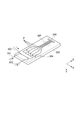
- FIG. 1 is an exploded perspective view illustrating a detection unit of the measurement apparatus.
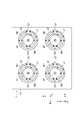
- FIG. 2 is a perspective view of a medium introduction system provided with a plurality of medium flow paths.
- FIG. 3 is a perspective view of a measurement unit including a plurality of detection units.
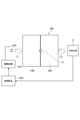
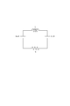
- FIG. 4 is a block diagram of the measuring device.
- FIG. 5 is a plan view of an antireflection film in the metamaterial optical member.
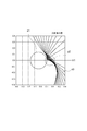
- FIG. 6 is a graph showing the relationship between the distance r and the effective refractive index n eff .
- FIG. 7 is a graph showing the relationship between the position L ( ⁇ m) in the antireflection film and the effective refractive index n eff .
- FIG. 8 is a perspective view showing a laminated structure in the antireflection film.
- FIG. 8 is a perspective view showing a laminated structure in the antireflection film.
- FIG. 9 is a graph showing the relationship between the dimension Lx in the length direction and the effective refractive index n eff in the laminated structure.
- FIG. 10 is a graph showing the chromatic dispersion value of the principal value of the dielectric constant tensor obtained from the effective medium theory when the volume ratio of silver to germanium is 0.4: 0.6 in the laminated structure.
- FIG. 11 is a graph showing the relationship between the wavelength ⁇ of incident light and the reflectance Rp (%) when there is no antireflection film.
- FIG. 12 is a graph showing the relationship between the wavelength ⁇ of incident light and the reflectance Rp (%) when an antireflection film is provided.
- FIG. 13 is a plan view of the metamaterial optical member.
- FIG. 14 is a diagram illustrating a path of light traveling in the metamaterial optical member on the input side.
- FIG. 15 is a plan view of the metamaterial optical member on the output side.
- FIG. 16 is a diagram for explaining the path of light passing through the detection unit of the measurement apparatus.
- FIG. 17 is a plan view of an input-side metamaterial optical member (improved example).
- FIG. 18 is a plan view of the metamaterial optical member (modified example) on the input side.
- FIG. 19 is a diagram for explaining the progress of light in the case of the structure of FIG.
- FIG. 20 is a plan view of a resonant metamaterial structure.
- FIG. 21 is an equivalent circuit diagram of a resonant metamaterial structure.
- FIG. 22 shows the relationship between the angular frequency ⁇ of incident light and the magnetic permeability ⁇ in a resonant metamaterial structure.
- FIG. 23 is a perspective view of a metamaterial structure including a rod pair array.
- FIG. 24 is a diagram showing current generated in the rod pair array.
- FIG. 25 is a perspective view of a mesh-like metamaterial structure.
- FIG. 26 is a diagram for explaining a path of light incident on an object in the implementation apparatus.
- FIG. 27 is a diagram for explaining a path of light incident on an object in the implementation apparatus.
- FIG. 28 is a diagram for explaining a path of light incident on an object in the implementation apparatus.
- FIG. 29 is a diagram for explaining a path of light incident on an object in the implementation apparatus.
- FIG. 29 is a diagram for explaining a path of light incident on an object in the implementation apparatus.
- FIG. 30 is a plan view of a metamaterial optical member of a type with a flat light exit surface.
- FIG. 31 is a diagram illustrating a relationship between a metamaterial optical member and an object.
- FIG. 32 is a diagram for explaining a path of light incident on an object in the implementation apparatus.
- FIG. 33 is a diagram for explaining a path of light incident on an object in the implementation apparatus.
- FIG. 34 is a diagram for explaining a path of light incident on an object in the implementation apparatus.
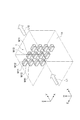
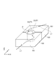
- FIG. 35 is a perspective view of the implementation apparatus.
- FIG. 36 is a diagram for explaining a path of light incident on an object in the light detection device.
- FIG. 37 is a diagram for explaining a path of light incident on an object in the light detection device.
- FIG. 38 is a diagram for explaining a path of light incident on an object in a laser excitation light source.
- FIG. 39 is a diagram illustrating a path of light traveling in the metamaterial optical member on the input side.
- FIG. 40 is a diagram illustrating a path of light traveling in the metamaterial optical member on the input side.
- FIG. 41 is a diagram illustrating a path of light traveling in the metamaterial optical member on the input side.
- FIG. 42 is a diagram for explaining the Zhukovski transformation.
- FIG. 43 is a diagram for explaining a light beam group (hook refractive index distribution) before and after conversion.
- FIG. 44 is a diagram for explaining a light beam group in the vicinity of the transparent cloak.
- FIG. 39 is a diagram illustrating a path of light traveling in the metamaterial optical member on the input side.
- FIG. 40 is a diagram illustrating a path of light traveling in the metamaterial optical member on the input side.
- FIG. 41 is a diagram illustrating a
- FIG. 45 is a diagram for explaining a light beam group (Kepler refractive index distribution) before and after conversion.
- FIG. 46 is a diagram for explaining a light ray group near the transparent cloak.
- FIG. 47 is a diagram for explaining a light ray group in the vicinity of the transparent cloak.
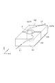
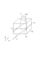
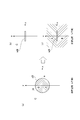
- FIG. 1 is an exploded perspective view showing a detection unit of the measurement device.
- an XYZ three-dimensional orthogonal coordinate system is set.
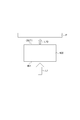
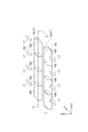
- the first metamaterial optical member 100 includes a condensing optical member 1 and an antireflection film 2 provided on the light exit surface of the condensing optical member 1.
- the condensing optical member 1 includes a light incident surface IN1 (XZ surface) on which incident light L1 is incident, and a light emitting surface OUT1 that faces the light incident surface IN1 and emits emitted light L10.
- An antireflection film 2 is provided on OUT1.
- the light exit surface OUT1 is a semi-cylindrical concave surface with the Z axis as the central axis. Note that the opening angle of the arc around the central axis of the concave surface may not be 180 degrees. In FIG.
- the antireflection film 2 is provided only on the concave surface, but may be provided on the entire surface of the XZ surface on the light emitting side in addition to the concave surface. Further, an antireflection film may be provided on the light incident surface IN1.
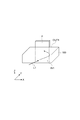
- the second metamaterial optical member 200 includes a light transmission member 1A and an antireflection film 2A provided on the incident surface of the light transmission member 1A.
- the structure of the light transmission member 1A is the same as that of the condensing optical member 1 including the internal refractive index distribution.
- the light transmitting member 1A is different from the condensing optical member 1 in that the light transmitting member 1A has a function of diffusing light incident from the concave light incident surface IN2 toward the light emitting surface OUT2.
- the object P is disposed between the pair of metamaterial optical members 100 and 200.
- the target P is a tube that forms a medium flow path.
- Various types of media FD in the tube flow.
- the light L1 incident from the light incident surface IN1 of the first metamaterial optical member 100 is condensed in the concave direction by the condensing optical member 1, and is transmitted to the outside through the antireflection film 2 from the light emitting surface OUT1. Emitted.
- the emitted light L10 is incident on the object P and is transmitted therethrough, and the light L20 is incident on the inside from the light incident surface IN2 of the second metamaterial optical member 200 via the antireflection film 2A.
- the light travels while diffusing inside the transmission member 1A, and is emitted to the outside as the outgoing light L2 from the light outgoing surface OUT2.
- Examples of the light L20 include transmitted light, scattered light, and fluorescence.
- the medium FD in the object P flows in the Z-axis direction.
- the flowing direction of the medium FD may be along the vertical direction, but may be along the horizontal direction.
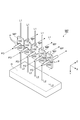
- FIG. 2 is a perspective view of a medium introduction system provided with a plurality of medium flow paths.
- the measuring device can include a medium introduction system as shown in FIG.
- a medium introduction system a plurality of medium flow paths (tubes) to be measured P are arranged on a substrate 300, and each tube has an input tube 301 for introducing a medium into the tube. 302 and a medium output tube 303 for outputting a part of an unnecessary medium.
- a medium to be measured is introduced into the tube 301, and a diluent is introduced into the tube 302.
- Examples of the medium to be introduced include ultrafine environmental hormones (exogenous endocrine disrupting substances / exogenous endocrine disrupting chemical substances), blood or saliva collected from a living body, bacteria or viruses. Depending on the size and characteristics of the substance to be examined, a reaction with a specific reagent can be caused, or a labeling reagent such as a fluorescent label can be attached. In this apparatus, by detecting the light transmitted through the medium, it is possible to determine the amount of influenza virus, O157, Salmorela, dioxin, stress markers, etc. contained in the liquid flowing in the medium flow path and determine the presence or absence thereof. . The blood glucose level and lipid level can also be used for testing metabolic syndrome.
- the medium introduced into the tube is mixed with a diluent or a necessary liquid, and then mixed with a labeling reagent or a reaction reagent introduced from the reagent introduction unit 304, flows in the medium flow path, and reaches the detection unit MP. .
- the detection unit MP In the detection unit MP, light transmitted through the tube is detected.
- the type of reagent can be different for each of the plurality of medium flow paths.
- a discharge section 305 is provided for sucking or discharging the medium flowing through the tube to the outside. An inspection using a gas as a medium is also possible.
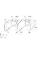
- FIG. 3 is a perspective view of a measurement unit including a plurality of detection units MP.
- each detection unit MP is as shown in FIG. 1, but a structure other than that shown in FIG. 1 is also applicable as long as it has a pair of metamaterial optical members.
- a plurality of detection units MP are aligned along the X-axis direction, and light L1 is incident on the light incident surface of the metamaterial optical member 100 on the input side of each detection unit MP and is transmitted through the object P.
- the light L2 is emitted from the light emitting surface of the metamaterial optical member 200 on the output side along the Y-axis direction.
- the emitted light L2 is detected by the photodetector D disposed to face the light emitting surface of the metamaterial optical member 200.
- a solid-state imaging device composed of a CCD image sensor or a MOS type image sensor can be used, but a plurality of photodiodes or photomultiplier tubes for detecting the light L2 output from each detector MP, respectively. It is also possible to use.
- the object P is a medium flow path
- the medium FD flows therethrough, and a signal corresponding to the characteristics of the medium FD flowing through each medium flow path is output from the detector D.
- the light L2 includes fluorescence and excitation light depending on the amount of the component. It will be. Therefore, since the excitation light can be cut by the second metamaterial optical member 200 by designing the second metamaterial optical member 200 according to the fluorescence wavelength, the light emission surface of the second metamaterial optical member 200
- the light L2 emitted from OUT2 can be only a fluorescent component.
- An optical filter that selectively transmits fluorescent components may be disposed on the surface of the photodetector D.
- the amount of the transmitted light L2 decreases according to the amount of the particles, so that the characteristics of the medium FD flowing through the respective medium flow paths from the photodetector D.
- a signal corresponding to (particle amount) is output.
- FIG. 4 is a block diagram of the measuring device.
- the object P is disposed between the pair of metamaterial optical members 100 and 200, and the light L2 transmitted through the object P enters the photodetector D.
- the output signal of the photodetector D is input to the control device 403 and stored in the internal storage device.
- the control device 403 is a computer and outputs a control signal to the drive circuit 401 to supply a drive current from the drive circuit 401 to the light emitting element 300. From the light emitting element 400, the incident light L1 to the metamaterial optical member 100 of the detection part MP is output.
- the light emitting element 400 is a laser diode, but a light emitting diode or the like can also be used.
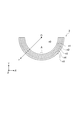
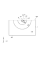
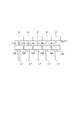
- FIG. 5 is a plan view of the antireflection film 2 in the metamaterial optical member 100 on the input side.
- the antireflection film 2 has an arc shape in the XY plane, and has a semicylindrical shape with the Z axis as the central axis as a whole.
- the concave surface inside the antireflection film 2 forms a semi-cylindrical surface, but the opening angle of the arc in the XY plane may not be 180 degrees.
- the central axis of this arc is the Z axis, and the position of the central axis is the origin O in the XY plane.
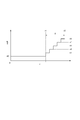
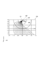
- FIG. 6 is a graph showing the relationship between the distance r and the effective refractive index n eff .
- the antireflection film 2 is formed by laminating layers having refractive indexes n1, n2, n3, n4, and n5 from the inside.
- the reference numerals of the layers n1 to n5 are the same as the refractive index.
- the refractive index in the antireflection film 2 increases in steps as the distance r increases (n0 ⁇ n1). ⁇ N2 ⁇ n3 ⁇ n4 ⁇ n5).
- the antireflection film 2 of this example has a five-stage refractive index distribution, this is not limited to five stages as long as it has a refractive index distribution that changes in multiple stages. .
- the position of the distance r ⁇ b> 1 indicates the position of the inner surface of the antireflection film 2
- the distance r ⁇ b> 2 indicates the position of the outer surface of the antireflection film 2.
- the refractive index can be changed in multiple steps along the position L ( ⁇ m) in the thickness direction of the antireflection film 2, where the position of the distance r1 is 0 and the direction from the distance r1 to the distance r2 is positive.
- FIG. 7 is a graph showing the relationship between the position L ( ⁇ m) in the thickness direction of the antireflection film 2 and the effective refractive index n eff .
- n0 is the refractive index of the outer medium (air)
- ns is the refractive index of the metamaterial optical member 100 on the light exit surface OUT1.
- the refractive index of the metamaterial optical member 100 and the antireflection film 2 can be 0-40.
- the region A of the innermost layer of the antireflection film 2 shown in FIG. 5 has a refractive index of n1.
- the layer having the refractive index n1 is obtained by arranging the regions A in a direction perpendicular to the thickness direction of the antireflection film.
- a layer having an arbitrary refractive index can be configured by arranging regions having a desired refractive index in a direction perpendicular to the thickness direction.
- a region having an arbitrary refractive index can be configured as follows.
- FIG. 8 is a perspective view showing a laminated structure of partial regions constituting a specific layer in the antireflection film 2.
- this partial region is represented by the above-described region A as a representative.
- the thickness direction of the layer n1 is set as the Y axis, and the directions perpendicular to the Y axis are set as the Z axis and the X axis, and incident light can travel in the Y axis direction.
- This stacked structure is formed by alternately stacking layers made of different materials.
- metal layers (Ag) and semiconductor layers (Ge) are alternately stacked.
- the thickness of one metal layer M is 4 nm, and the thickness of one semiconductor layer S is 6 nm.
- region A ′ having the same structure as the region A having a stacked structure is shown adjacent to the region A.
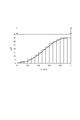
- FIG. 9 is a graph showing the relationship between the dimension L Z in the length direction (Z-axis direction) and the effective refractive index n eff in the stacked structure of FIG.
- the dimension L Y L Z in the height direction (Y-axis direction). That is, the shape of the light incident surface is a square.
- the effective refractive index n eff can be 35.7.
- Such a design method of refractive index and dielectric constant is described in, for example, “J. Opt. Soc. Am. B, Vol. 29, No. 9, 2559 (2012))”.
- FIG. 10 is a graph showing the chromatic dispersion value of the principal value of the dielectric constant tensor obtained from the effective medium theory when the volume ratio of silver to germanium is 0.4: 0.6 in the laminated structure.
- the relationship between the wavelength ⁇ (nm) and the effective dielectric constant ⁇ eff is shown.
- the volume ratio of Ag and Ge is 4: 6
- the real parts of the effective permittivity ⁇ Z and ⁇ X in the Z direction and the X direction are both ⁇ 9.8.
- the real part of the effective dielectric constant ⁇ Y in the Y direction can be 34.2.
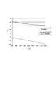
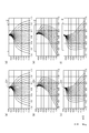
- FIG. 11 is a graph showing the relationship between the wavelength ⁇ of incident light and the reflectance Rp (%) when there is no antireflection film 2.
- the incident angles of incident light are 0 degrees, 15 degrees, and 30 degrees, and the reflectances of the p-polarized component and the s-polarized component included in the incident laser light are shown.
- the incident angle is 0 degree, the reflectance is about 89%, and at least 87% or more of the light is reflected even in the p-polarized light.
- FIG. 12 is a graph showing the relationship between the wavelength ⁇ of incident light and the reflectance Rp (%) when an antireflection film is provided.
- the incident angles of incident light are 0 degrees, 15 degrees, and 30 degrees, and the reflectances of the p-polarized component and the s-polarized component included in the incident laser light are shown.
- the calculation method of this graph is the same as described above.
- the reflectance is 1% or less, preferably 0.5% or less, in the wavelength range of 925 nm to 1075 nm, regardless of the polarization state.
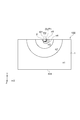
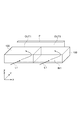
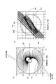
- FIG. 13 is a plan view of the metamaterial optical member 100.
- the refractive index is set so as to increase from the light incident surface IN1 toward the light emitting surface OUT1. That is, a high refractive index region n50 exists around the concave portion D1 provided with the antireflection film 2, and the region n40 is formed around the region n50, and the regions n30, n20, and n10 are sequentially arranged from the inside so as to surround them. Is located.
- the refractive index satisfies the relationship of n50> n40> n30> n20> n10, and these refractive indexes indicate the average refractive index in each region, and in each region, the recess D1 It is set higher as it gets closer.
- the desired refractive index can be realized using the metamaterial structure shown in FIG. 8 described above, but other structures can also be adopted.
- the refractive index distribution shown in FIG. 13 is called a hook refractive index distribution.
- FIG. 14 is a diagram illustrating a path of light traveling in the input-side metamaterial optical member 100 illustrated in FIG. 13, and a graph is superimposed on the position of the metamaterial optical member.
- This figure shows a light propagation path when the incident angle of light is 45 °.
- the dimension is displayed on the vertical axis
- the dimensional unit is not limited to millimeters, and may be centimeters, micrometers, or the like.
- the display of the antireflection film is omitted.
- the incident light travels in the right direction of the drawing, and is then collected while being bent to the left, and is collected on the inner surface of the recess D1 through the region n50 having the highest refractive index. Since an antireflection film (not shown) is provided at the condensing position, the collected light is output to the outside without being reflected at the interface.
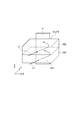
- FIG. 15 is a plan view of the metamaterial optical member 200 on the output side.
- the structure of the metamaterial optical member 200 on the output side is the same as that of the metamaterial optical member 100 on the input side, but is arranged at a symmetrical position with respect to the axis of the object P shown in FIG. Therefore, the metamaterial optical member 200 has a high refractive index around the recess D1, but the region with the highest refractive index is located on the left side of the drawing. Further, an antireflection film 2A is provided on the light incident surface IN2 which is the inner surface of the recess D1.
- FIG. 16 is a diagram for explaining the path of light passing through the detection unit MP of the measurement apparatus.
- the incident light L1 is incident on the object P via the first metamaterial optical member 100, and the light transmitted therethrough is transmitted to the outside as outgoing light L2 via the second metamaterial optical member 200. Is output.
- a slight gap is provided between the first metamaterial optical member 100 and the second metamaterial optical member 200, but these may be in contact with each other. In this case, it becomes difficult for light from the outside to enter the object P.
- FIG. 17 is a plan view of the metamaterial optical member 100 (an improved example) on the input side.
- This metamaterial optical member 100 differs from that shown in FIG. 13 only in that the antireflection film 3 is formed also on the light incident surface IN1. In this case, interface reflection at the light incident surface of incident light on the metamaterial optical member 100 can be suppressed.
- the antireflection film 3 is provided in a place where a large refractive index change does not occur, a normal antireflection film material may be used.
- the structure of the antireflection film 3 is any two selected from a silicon oxide film, a titanium oxide film, a tantalum oxide film, a niobium oxide film, a hafnium oxide film, an aluminum oxide film, or a magnesium fluoride film. It is possible to adopt a laminated structure in which are alternately formed.
- FIG. 18 is a plan view of the metamaterial optical member 100 on the input side (modified example).
- This metamaterial optical member 100 differs from that shown in FIG. 13 only in that a concave portion D2 having a smaller radius of curvature is formed on the inner surface of the concave portion D1.
- the recess D2 has a semi-cylindrical surface with the Z axis as the central axis, and the opening angle of the arc in the XY plane is 180 degrees, but the opening angle is not limited to 180 degrees.
- FIG. 19 is a diagram for explaining the progress of light in the case of the structure of FIG.
- the light that has entered the condensing optical member 1 from the light incident surface IN1 is condensed toward the concave portion D1.
- the light is condensed toward the concave portion D2 located on the inner surface of the concave portion D1.
- the concave portion D2 can be produced by removing a part of the concave portion D1 of the condensing optical member 1 up to a region slightly before the condensing position.
- the concave surface of the concave portion D1 is an arc that forms part of a circle in the XY plane, but the concave surface of the concave portion D2 is also an arc that forms part of a circle in the XY plane.
- the condensed light is emitted into the concave portion D1 as outgoing light L10 through the concave portion D2.
- the antireflection film may be formed at least on the inner surface of the concave portion D2 related to light emission, but may be formed on the entire inner surface of the concave portion D1 or the surface facing the light incident surface IN1.
- the light emission surface OUT1 is continuous with a part of the concave surface constituting the concave portion D1, and includes the concave surface (second concave surface) of the concave portion D2 having an opening size smaller than the opening size of the concave surface.
- the opening size is defined by the length of a line segment connecting both ends of the arc in the XY plane.
- the condensing position is located deeper in the condensing optical member 1 than the concave surface of the concave portion D1, the second concave surface in which the condensing position is located inside is partially provided. Since the aperture size is small, it can be formed without processing many portions of the condensing optical member 1.
- FIG. 20 is a plan view of the resonance type metamaterial structure, and shows a state of a partial region of the condensing optical member 1.
- the light is traveling in the Y-axis direction, and the traveling direction of the light is indicated by a wave vector k, it is assumed that an electric field and a magnetic field are generated in a direction perpendicular thereto.
- the electric field vector E and the magnetic field vector H are orthogonal to each other, and both are perpendicular to the wave vector k.
- the condensing optical member 1 designs a refractive index in consideration of the point.
- the wave vector k matches the Y axis
- the magnetic field vector H matches the Z axis
- the electric field vector E is parallel to the X axis.
- the condensing optical member 1 includes an insulator 1X made of an insulating layer parallel to the XY plane, and rings M1 and M2 formed on the insulator 1X.
- the insulator 1X can be made of an inorganic insulator such as SiO 2 or SiN x, but an organic material such as a resin can also be used.
- the rings M1 and M2 are made of a conductor, and preferably made of metal. In the figure, a part of the pair of rings M1, M2 is cut, and gaps G1, G2 are formed in the cut parts.
- FIG. 21 is an equivalent circuit diagram of a resonant metamaterial structure.
- the metamaterial structure shown in FIG. 20 can be expressed by the transmission circuit of FIG. Capacity is two and C 0/2 of the capacitor, the coil inductance L, a coil of resistance R LC resonant circuit is constituted.
- the coil is a ring M1. It is comprised by M2.
- FIG. 22 shows the relationship between the angular frequency ⁇ of incident light and the effective magnetic permeability ⁇ eff in a resonant metamaterial structure.
- the effective permeability ⁇ eff changes according to the wavelength ⁇ or the angular frequency ⁇ .
- the solid line indicates the real part ⁇ Re ( ⁇ ) of the magnetic permeability at a certain angular frequency ⁇
- the dotted line indicates the imaginary part ⁇ Im ( ⁇ ) of the magnetic permeability.
- the imaginary part of the magnetic permeability ⁇ is maximized and the real part is zero.
- the real part of the magnetic permeability is negative, the imaginary part is positive, and the overall magnetic permeability ⁇ ⁇ 0.
- the real part of the magnetic permeability is positive and the imaginary part is also positive, and the overall magnetic permeability ⁇ > 0.
- the resonance angular frequency ⁇ 0 increases as the inductance L and the capacitance of the capacitor in the LC resonance circuit are reduced.
- the resonance frequency ⁇ 0 it is possible to function as a material having different permeability (refractive index / permeability square root) for light of the same wavelength ⁇ .
- a metamaterial structure having a desired refractive index can be produced.
- the material constituting the conductor having the metamaterial structure includes metals such as Au, Pt, Ag, Cu, Ti, and Al, nitrides such as TiN, TaN, HfN, and ZrN, or ITO, ZnO: Al.
- a transparent conductive film such as ZnO: Ga can be preferably used.
- the metamaterial structure shown in FIG. 20 constitutes a split ring type resonator, but a metamaterial structure including a rod pair array can also be adopted.
- FIG. 23 is a perspective view of a metamaterial structure including a rod pair array, and shows a state of a partial region of the condensing optical member 1.
- This structure is obtained by changing the above split ring type ring shape into a pair of opposing rods M11 and M12 in the condensing optical member 1, and arranging a plurality of rod pairs.
- Each of the rods M11 and M12 is made of a conductor and has a plate shape, but may be a cylinder or a polygonal column.
- the rods M11 and M12 are embedded in the insulator 1X.
- the light travels along the wave vector k with the traveling direction of the incident light L1 as the Y axis, and the magnetic field vector H and the electric field vector E are orthogonal to the traveling direction of the light. Since the direction of these vectors changes with the progress of light, the condensing optical member 1 designs the refractive index in consideration of this point.
- the wave vector k matches the Y axis
- the magnetic field vector H matches the Z axis
- the electric field vector E is parallel to the X axis.
- the rods M11 and M12 extend along the X-axis direction (electric field vector E direction), and the rod pairs are two-dimensionally arranged in the XZ plane.
- the rod pairs are also arranged along the Y-axis direction, but the illustration is omitted.
- Incident light L1 is refracted by the rod pair and is emitted as outgoing light L10.
- FIG. 24 is a diagram showing current generated in the rod pair array.
- the insulator 1X is interposed between the rod M11 and the rod M12.
- an electric field vector E and a magnetic field vector H are generated in a direction perpendicular to the wave vector k.
- a counter magnetic field is generated so as to cancel the magnetic field in the direction of the magnetic field vector H, and a displacement current J flows in the direction of the arrow. Since an equivalent circuit of this structure can constitute an LC resonator, the refractive index can be controlled in the same manner as a split ring resonator.
- FIG. 25 is a perspective view of a mesh-like metamaterial structure.
- This metamaterial structure extends the rod pair array shown in FIG. 24 in the Z direction (corresponding to the H direction), and in addition to the rod pair array (rods M31 and M32) that extends in the vertical direction, corresponds to the X direction (corresponding to the E direction). It can also be considered that the rod pair array (rods M21 and M22) extends in the lateral direction.
- An insulator 1X is interposed between the pair of rods M21 and M22 extending in the horizontal direction and between the pair of rods M31 and M32 extending in the vertical direction.
- rods M21 and M31 or rods M22 and M32 are shown as separate members for convenience of explanation, but they may be integrated. In this case, the insulator 1X is disposed between the mesh-like conductors.
- the longitudinally extending rod pair array can constitute an LC resonator like the above-described split ring type resonator, and therefore has a structure that responds to a magnetic field, and thus the permeability can be controlled. Further, the rod pair array extending in the lateral direction has a structure that responds to an electric field as shown in FIG. 8, and can control the dielectric constant.
- FIG. 25 can be said to be a structure that responds to both an electric field and a magnetic field. If the structure of FIG. 25 is regarded as one “unit cell”, a structure that operates in a wide region (area) can be manufactured by arranging the unit cells vertically and horizontally. This structure is known as a fishnet structure because of its shape (Nature, Vol.
- the unit cell has a very small size of about 1/6 or less of the incident wavelength, and thus acts as an atom or molecule with respect to the incident light. Therefore, light can be transmitted and refracted.
- the traveling direction of light is represented by a wave vector k and is perpendicular to both the electric field vector E and the magnetic field vector H.
- the apparatus that does not use the metamaterial optical member on the output side ends its optical role when the condensed light is incident on the object P.
- a photodetector When a photodetector is used as the object P, it can function as a photodetector for detecting light that has passed through the input-side metamaterial optical member.
- a laser medium When a laser medium is used as the object P, it can function as a laser excitation light source that emits laser light by condensing excitation light that has passed through the input-side metamaterial optical member to excite the laser medium.
- a resonator can be configured by installing mirrors and half mirrors at both ends of the laser medium.
- FIG. 26 is a diagram for explaining a path of light incident on an object in the implementation apparatus.
- the object P has a columnar shape that can be placed in the above-described recess.
- This device functions as a light detection device when the object P is a light detector, and functions as a laser excitation light source when it is a laser medium.
- the incident light L1 to the metamaterial optical member 100 initially travels in the direction of 45 degrees diagonally to the right. However, the incident light L1 travels in the direction from the middle to the left, is condensed, escapes from the concave portion, and reaches the object P. To do.
- FIG. 27 is a diagram for explaining a path of light incident on an object in the implementation apparatus.
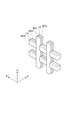
- This structure is obtained by stacking two metamaterial optical members 100 along the Z-axis direction in the implementation apparatus shown in FIG.
- the incident light L1 can be incident on the object P.
- the operation of this apparatus is the same as that shown in FIG. Since the metamaterial optical members 100 are arranged in the vertical direction, a line sensor can be used as a photodetector, and a plurality of types of elements can be stacked as a laser medium to be used as a multi-wavelength excitation light source.
- FIG. 28 is a diagram for explaining a path of light incident on an object in the implementation apparatus.
- This structure is obtained by arranging two metamaterial optical members 100 along the X-axis direction in the implementation apparatus shown in FIG. In the case of this structure, even when the number of objects P is two, the incident light L1 can be incident on each object P.
- the operation of this apparatus is the same as that shown in FIG.
- a plurality of line sensors can be used as the plurality of objects P.
- FIG. 29 is a diagram for explaining a path of light incident on an object in the implementation apparatus.
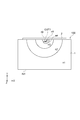
- FIG. 30 is a plan view of a metamaterial optical member having a flat light exit surface.
- this metamaterial optical member 100 is not provided with a recess, the light exit surface OUT1 is a flat surface, and the antireflection film 2 is The remaining configuration is the same as that of the light emitting surface OUT1. Since a flat surface is used as the light emitting surface, a region n6 having a high refractive index is provided in the region where the recesses existed in FIG. The region n6 is located inside the region n5, and the refractive index satisfies n5 ⁇ n6. For convenience of explanation, the same reference numerals are used for the respective regions and the refractive index.
- the region n6 Since the region n6 has the highest refractive index in the metamaterial optical member 100, the light incident from the light incident surface IN1 passes through the metamaterial optical member 100 and reaches the light exit surface OUT of the region n6. Is condensed. The light condensed on the light exit surface OUT1 passes through the antireflection film whose refractive index gradually decreases along the positive direction in the Y-axis direction, and exits to the outside. Gas (air) exists outside.
- the region n6 may be a region having a constant high refractive index, but may have a refractive index distribution in which the refractive index gradually increases in the light collecting direction.
- an antireflection film can also be provided on the light incident surface side, applied to various devices, or a plurality of metamaterial optical members 100 can be combined.
- FIG. 31 is a diagram showing the relationship between the metamaterial optical member and the object.
- the light L1 incident from the light incident surface IN1 of the metamaterial optical member 100 passes through the inside and is emitted from the light emitting surface OUT, and the light L10 transmitted through the metamaterial optical member 100 reaches the object P.
- the metamaterial optical member 100 and the object may be in close contact with each other, but may be separated from each other.
- a plate-like object that can be easily opposed to a flat surface can be used in addition to the columnar object that can be disposed in the above-described recess.
- the object P may be a physically integrated solid, or may be a plurality of separated elements.
- a solid-state imaging device such as a CCD image sensor or a MOS type image sensor can be used as the photodetector.
- a line sensor may be used in addition to a two-dimensional image sensor.
- FIG. 32 is a diagram for explaining a path of light incident on an object in the implementation apparatus.
- the object P has a plate-like shape, and when the light emitting surface OUT1 of the metamaterial optical member 100 is a flat surface, the object P is easily arranged on the metamaterial optical member 100. be able to.
- This device functions as a light detection device when the object P is a light detector, and functions as a laser excitation light source when it is a laser medium.
- the incident light L1 to the metamaterial optical member 100 initially travels in the direction of 45 degrees diagonally to the right. However, the incident light L1 travels in the direction from the middle to the left, is condensed, escapes from the concave portion, and reaches the object P. To do.
- FIG. 33 is a diagram for explaining a path of light incident on an object in the implementation apparatus.
- This structure is obtained by stacking two metamaterial optical members 100 along the Z-axis direction in the implementation apparatus shown in FIG. In the case of this structure, even when the dimension of the object P in the Z-axis direction is increased, the incident light L1 can be incident on the object P.
- the operation of this apparatus is the same as that shown in FIG. Since the metamaterial optical members 100 are arranged in the vertical direction, a line sensor can be used as a photodetector, and a plurality of types of elements can be stacked as a laser medium to be used as a multi-wavelength excitation light source.
- FIG. 34 is a diagram for explaining a path of light incident on an object in the implementation apparatus.
- This structure is obtained by arranging two metamaterial optical members 100 along the X-axis direction in the implementation apparatus shown in FIG.
- the incident light L1 can be incident on the object P even when the dimension of the object P in the X-axis direction is increased or the number is increased to 2 or more.
- the operation of this apparatus is the same as that shown in FIG.
- As the object P it is preferable to use a line sensor or the like extending in the X-axis direction.
- FIG. 35 is a perspective view of the implementation apparatus.
- a plurality of metamaterial optical members 100 are arranged along the X-axis direction, and arranged so as to sandwich both ends of the object P in the Y-axis direction.
- the incident light L1 is made to enter from different directions. In the case of this structure, higher-density incident light L1 can be input to the object P.
- the operation of this apparatus is the same as that shown in FIG.
- the object P is a laser medium
- the shape of the laser medium is a rectangular parallelepiped extending in the X-axis direction
- the metamaterial optical member 100 is disposed in the vicinity of two opposing XZ planes.
- a laser excitation light source having this structure can also be used as a driver for laser fusion.
- an excitation laser (wavelength 804 nm) can be used as the incident light L1
- HAP4 Nd-added phosphate glass) can be used as the laser medium.
- FIG. 36 is a diagram for explaining a path of light incident on an object in the light detection device.
- a plurality of metamaterial optical members 100 are arranged in a row facing the object P.
- the object P is a line sensor.
- the condensed light L10 is emitted from the metamaterial optical member 100 in accordance with the amount of light L1 incident on each metamaterial optical member 100, and is incident on the line sensor.
- the line sensor outputs a one-dimensionally distributed optical image signal.
- FIG. 37 is a diagram for explaining a path of light incident on an object in the light detection device.
- each object P is a photodiode or a photomultiplier tube.
- the condensed light L10 is emitted from the metamaterial optical member 100 in accordance with the amount of light L1 incident on each metamaterial optical member 100, and is incident on the line sensor.
- the line sensor outputs a one-dimensionally distributed optical image signal.
- FIG. 38 is a diagram for explaining a path of light incident on an object in a laser excitation light source.
- the incident light L1 enters the metamaterial optical member 100 via the light incident surface IN1, is condensed inside, is emitted from the light emitting surface OUT1 as the emitted light L10, and is incident on the end surface of the object P.
- the object P is a laser medium and also an optical waveguide such as an optical fiber.
- laser light for excitation light can be incident on the light incident surface IN1 from multiple directions.
- the metamaterial optical member 100 can collect light incident from a plurality of directions at substantially the same position, and can function as a coupler of a plurality of excitation lights into one optical fiber.
- FIG. 39 is a diagram showing a path of light traveling in the metamaterial optical member on the input side, and a graph is superimposed on the position of the metamaterial optical member.
- the dimension is displayed on the vertical axis
- the incident light is incident on the light incident surface at 0 degree.
- the light incident on the light incident surface is condensed toward the recess D1. Since an antireflection film (not shown) is provided at the condensing position, the collected light is output to the outside without being reflected at the interface.
- FIG. 40 is a diagram showing a path of light traveling in the metamaterial optical member on the input side, and a graph is superimposed on the position of the metamaterial optical member.
- the dimension is displayed on the vertical axis
- the incident light is incident on the light incident surface at 45 degrees opposite to that in the case of FIG.
- the light incident on the light incident surface is condensed toward the recess D1.
- the incident light travels in the left direction of the drawing, and is then collected while being bent to the right, and is collected on the inner surface of the recess D1 through the region n40. Since an antireflection film (not shown) is provided at the condensing position, the collected light is output to the outside without being reflected at the interface.
- FIG. 14, FIG. 39 and FIG. 40 described above have described the case where the refractive index inside the metamaterial optical member is caused by the refractive index distribution of the hook, this may be another distribution.
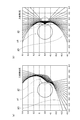
- FIG. 41 is a diagram showing a light path when the refractive index distribution of the metamaterial optical member is caused by the Kepler refractive index distribution, and the graph is superimposed on the position of the metamaterial optical member.
- 41A shows a case where the incident angle is 0 degree
- FIG. 41B shows a case where the incident angle is 45 degrees
- FIG. 41C shows a case where the incident angle is ⁇ 45 degrees.
- the incident light is collected toward the recess D1 in FIG.
- a recess D1 in FIG. 41 exists at a position adjacent to the recess, instead of the recess D1 (position indicated by a dotted line) shown in FIG. 13 and the like, and has a smaller radius than the recess.
- the inner surface of the recess D1 is a light emitting surface, and an antireflection film 2 (not shown) is provided on the inner surface (semi-cylindrical concave surface). Incident light that has passed through the antireflection film 2 is emitted outward from the inner surface of the recess.
- the opening angle of the arc constituting the inner surface of the recess D1 is 180 degrees, but may be an angle other than this.
- 41 (d), 41 (e), and 41 (f) respectively show the light exit surface without providing the concave portion when the incident angle is 0 degree, 45 degrees, and -45 degrees.
- the structure of the antireflection film 2 is the same as that shown in FIG.
- the incident light is collected in a specific region regardless of the direction of the incident light.
- a cloaking device transparent cloak
- an antireflection film is disposed in the vicinity of the cloaking region in the cloaking device, and light (electromagnetic wave) is extracted from the outside (outside the cloaking region).
- a concave portion is provided in the vicinity of the cloaking region and an antireflection film is disposed in the concave portion.
- the antireflection film is disposed so that the vicinity of the cloaking region is a flat surface. .
- the refractive index distribution may be designed to guide the light as it is.
- “New J. Phys, vol. 8, 118 (2006)” is known as a method for calculating a light path when there is a refractive index gradient.
- the conformal mapping method is a method for obtaining a ray trajectory by approximately solving a wave equation with a Helmholtz equation in a complex plane. This is a method in which a real space is a physical space (z plane) and a temporary space used for ease of design is a virtual space (w plane), and the two spaces are combined by an equiangular mapping. It is.
- the conformal mapping method for example, the Zhukovsky transformation can be used.
- the Zhukovsky transformation is used when designing in the virtual space in order to easily design in the physical space.
- the Zhukovsky transformation is an equiangular mapping that transforms physical space (z plane) into virtual space (w plane).
- the design using the optical conformal mapping method is useful when designing a metamaterial optical member using an isotropic medium, and coordinate transformation is required for designing a metamaterial optical member using an anisotropic medium. This is useful when using the method.
- FIG. 42 is a diagram for explaining the Zhukovsky transformation.
- w u + jv) (j is an imaginary unit). Since these planes are complex planes, the horizontal axis is set as the real axis, and the vertical axis is set as the imaginary axis.
- c) is converted into a line segment wB.
- the region C outside the circle zB having the radius a becomes a region C that fills the periphery of the line segment wB in FIG. 42B after conversion (FIG. 42B).
- the upper region B inside the circle zB having the radius a in FIG. 42A becomes the lower region B of the line segment zB in FIG. 42C after conversion.
- the lower region A inside the circle zB having the radius a in FIG. 42A becomes the upper region A of the line segment zB in FIG.
- the virtual space function is a multivalent function, which is the w-plane of the virtual space sharing the line segment wB (see FIG. 42 (b) and FIG. 42 (c)) can be overlapped and displayed as a Riemann surface.
- the hook refractive index distribution (refractive index distribution by the hook harmonic vibration profile method) and the Kepler refractive index distribution (refractive index distribution by the Kepler profile method) are shown in the virtual space.
- the distribution is a refractive index distribution according to the following formula.
- the region having the radius r 0 can be made to correspond to the circle z1 that is the hollow region described above.
- n ′ 2 1 ⁇
- n ′ is the refractive index in the lower Riemann sheet in the virtual space
- r 0 is the radius value used to define the cloaking area
- w is a point on the lower Riemann sheet in the virtual space
- W 1 is the value of the branch point in the virtual space.
- Kepler refractive index distribution is a refractive index distribution according to the following formula.
- n ′ 2 r 0 /
- n ′ is the refractive index in the lower Riemann sheet in the virtual space
- r 0 is the radius value used to define the cloaking area
- w is a point on the lower Riemann sheet in the virtual space
- W 1 is the value of the branch point in the virtual space.
- FIG. 43 is a diagram for explaining a light beam group (hook refractive index distribution) before and after conversion.
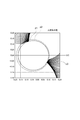
- FIG. 43 (a) is a diagram showing a ray trajectory group in a cloaking device in a physical space and a line group necessary for designing the present invention, and scales are drawn on the vertical axis and the horizontal axis.
- the unit of the vertical axis and the unit of the horizontal axis are, for example, millimeters. If light is incident on the metamaterial optical material from the lower side of the drawing at an incident angle of 45 degrees, if this is a cloaking device, light does not enter the inside of the circle z1 near the origin, and the light bends near the circle z1. Then, it is output to the outside as an outgoing light beam.
- a circle z2 is drawn with a dotted line slightly outside the circle z1, and the metamaterial optical member is cut along the horizontal line H1 passing through the center of the circle z1 to remove the upper portion, and further up to the position of the circle z2 If the removal is performed, the incident light is exposed to the outside in the vicinity of the condensing position before being bent in the vicinity of the circle z1.
- An enlarged view of the ray path in the vicinity of the circle z2 is shown in FIG. By providing an antireflection film at this condensing position, the condensed light can be extracted to the outside.
- FIG. 43 (a) the circle zB having the radius a described above is shown.
- FIG. 43 (b) is a diagram showing a light ray path in the virtual space, and the vertical axis and the horizontal axis are graduated.
- the unit of the vertical axis and the unit of the horizontal axis are, for example, millimeters.
- the circle zB in FIG. 43A is converted to the line segment wB in FIG. 43B by the Zhukovsky transformation.
- Circles z1 and z2 located inside the circle zB are converted into circles w1 and w2 in the virtual space, respectively.
- the ray path z4 outside the circle zB in the physical space and the ray path z3 inside are converted into the parallel ray group w4 and the annular ray group w3 in the virtual space, respectively.
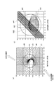
- FIG. 45 is a diagram for explaining a light beam group (Kepler refractive index distribution) before and after conversion.
- FIG. 45 (a) is a diagram showing a light beam path in the physical space, and the vertical axis and the horizontal axis are graduated.
- the unit of the vertical axis and the unit of the horizontal axis are, for example, millimeters. If light is incident on the metamaterial optical material from the lower side of the drawing at an incident angle of 45 degrees, if this is a cloaking device, light does not enter the inside of the circle z1 near the origin, and the light bends near the circle z1. Then, it is output to the outside as an outgoing light beam. Incident light is collected near a specific position on the horizontal line H1 that crosses the circle z1.
- FIG. 46 shows an enlarged view of the light path near the circle z1.
- the condensed light can be extracted to the outside.
- FIG. 46 it is also possible to perform processing for removing the region of the circle z2 surrounding the region including the vicinity of the condensing position, and to provide an antireflection film at the removed position.
- FIG. 45A the circle zB having the radius a described above is shown.
- FIG. 45 (b) is a diagram showing a light ray path in the virtual space, and the vertical axis and the horizontal axis are graduated.
- the unit of the vertical axis and the unit of the horizontal axis are, for example, millimeters.
- the circle zB is converted into the line segment wB in FIG. 45B by the Zhukovsky conversion.
- a circle z1 and a circle z2 located inside the circle zB are converted into circles w1 and w2 in the virtual space, respectively.
- the ray path z4 outside the circle zB in the physical space and the ray path z3 inside are converted into the parallel ray group w4 and the annular ray group w3 in the virtual space, respectively.
- FIG. 47 shows that the incident angle is 30 degrees (FIG. 47A) and the incident angle is 0 degrees (FIG. 47B).
- 2 shows a light beam path in the vicinity of the circle z1 (Kepler refractive index distribution).
- the light beam z3 is reflected by the circle z1, so that the upper region is cut by a horizontal line passing through the circle, or the region indicated by the circle z2 is further removed, and the vicinity of the exposed condensing position
- the condensed light can be extracted to the outside.
- the light beam path in the metamaterial optical member is designed using the Zukovsky transformation between the physical space and the virtual space and the inverse transformation. That is, the cloaking region is corrected by sequential calculation in order to obtain a necessary portion from the group of ray trajectories of the cloaking device using the optical conformal mapping method.
- the metamaterial optical member and the apparatus using the same according to the above-described embodiment have the following configurations and features.
- the first metamaterial optical member 100 includes a light collecting surface 1 having a light incident surface IN1 and a light emitting surface OUT1, and having a light collecting function, and a light emitting surface of the light collecting optical member 1.
- An antireflection film 2 provided on OUT1, and the antireflection film 2 has a first metamaterial structure whose refractive index gradually decreases along the light traveling direction (see FIGS. 6 and 7). .
- the refractive index of the region where the light is collected by the condensing optical member 1 is set higher than the peripheral region.
- the antireflection film 2 having the first metamaterial structure is provided so that the light condensed on the light exit surface OUT1 of the condensing optical member 1 is extracted outside without being reflected by the light exit surface OUT1. .
- the metamaterial structure it is possible to form a refractive index change from a high refractive index to a low refractive index that does not exist in nature, and thus light that could not be extracted to the outside can be extracted to the outside.
- the condensing optical member 1 gradually increases in refractive index from the light incident surface IN1 toward the light exit surface OUT1 (see FIG. 13). It has a metamaterial structure.
- the condensing optical member 1 since the condensing optical member 1 has the second metamaterial structure, a refractive index change that does not exist in the natural world can be formed. Can do light. Even when the light is condensed in such a special state, since the anti-reflection film 2 having the first metamaterial structure is provided, the light condensed on the light emitting surface OUT1 can be extracted to the outside.
- the light emission surface OUT1 includes a concave surface (concave portion D1) (FIG. 1).
- the collected light can be used in the inner space of the concave portion D1.
- the light emission surface OUT1 is a second concave surface (concave portion D2) that is continuous with part of the concave surface and has an opening size smaller than the concave opening size. ) (FIG. 18).
- a second concave surface in which the condensing position is located inside is partially provided. Since the second concave surface has a small opening size, it can be formed without processing many portions of the condensing optical member 1.
- the light emission surface OUT1 includes a flat surface (FIG. 30). In this case, there is an advantage that it is not necessary to perform a process of forming a concave surface on the light emitting surface OUT1.
- the first photodetection device using the metamaterial optical member according to the above-described embodiment is disposed inside the concave surface of the third or fourth metamaterial optical member 100 having the concave surface and the metamaterial optical member. And a photodetector.
- the photodetector a photomultiplier tube, a photodiode, a solid-state imaging device, or the like can be used.
- the 1st laser excitation light source concerning the above-mentioned embodiment is provided with the 3rd or 4th metamaterial optical member 100 which has the above-mentioned concave surface, and the laser medium arranged inside the concave surface of metamaterial optical member 100. ing.
- the excitation light of the laser medium is incident on the light incident surface IN1 of the condensing optical member 1, it is condensed and incident on the laser medium disposed inside the concave surface via the antireflection film 2. Therefore, the laser medium can be excited by the excitation light.
- an optical fiber to which a rare earth element such as Er, Yb, or Nd is added can be used as the laser medium.
- the first measurement apparatus includes the third or fourth metamaterial optical member 100 having the above-described concave surface, a medium flow path disposed inside the concave surface of the metamaterial optical member 100, and a medium And a photodetector for detecting light from the flow path (FIG. 1).
- Various substances to be inspected can flow in the medium flow path. For example, when a labeling substance that generates fluorescence when light of a specific wavelength is absorbed flows through the medium flow path, the light generated from the substance can be detected by a photodetector. Based on this, the substance can be analyzed.
- an opaque liquid is flowed as a medium, it is possible to inspect the transparency of the medium by detecting the amount of light transmitted through the medium.
- the second photodetection device includes the fifth metamaterial optical member 100 having the above-described flat surface, and a photodetector disposed to face the flat surface of the metamaterial optical member 100. Yes.
- the photodetector As the photodetector, a photomultiplier tube, a photodiode, a solid-state imaging device, or the like can be used. In particular, when the flatness of the flat surface is used, there is an advantage that the solid-state imaging elements are easily arranged to face each other.
- the 2nd laser excitation light source concerning the above-mentioned embodiment is provided with the 5th metamaterial optical member 100 which has the above-mentioned flat surface, and the laser medium arranged opposite to the flat surface of metamaterial optical member 100.
- the excitation light of the laser medium is incident on the light incident surface IN1 of the condensing optical member 1, it is condensed and enters the laser medium disposed opposite to the antireflection film 2 provided on the flat surface. . Therefore, the laser medium can be excited by the excitation light.
- the laser medium in addition to an optical fiber to which a rare earth element such as Er, Yb or Nd is added, a plate-shaped one having a flat opposing surface can be used.
- the second measurement apparatus detects the fifth metamaterial optical member 100, the medium flow path disposed opposite to the flat surface of the metamaterial optical member 100, and light from the medium flow path. And a photodetector.
- the substance to be inspected can be allowed to flow in the medium flow path.
- the photodetector can detect light generated from the substance in the medium flow path, and analysis of the substance can be performed based on the detected light.
- an opaque liquid is flowed as a medium, it is possible to inspect the transparency of the medium by detecting the amount of light transmitted through the medium.
- the second metamaterial optical member 200 used in combination with the first metamaterial optical member 100 can be used (FIG. 1).
- the second metamaterial optical member 200 on the light receiving side includes a light transmission member 1A having a light incident surface IN2 and a light emitting surface OUT2, and a reflection provided on the light incident surface IN2 of the light transmission member 1A.
- the light transmission member 1A includes the prevention film 2A, and the refractive index gradually decreases from the light incident surface IN2 toward the light emitting surface OUT2. Since the region on the light incident surface IN2 side has a high refractive index, light can easily enter from the outside.
- the antireflection film 2A When light is incident on the light incident surface IN2 of the light transmission member 1A from the outside, the antireflection film 2A functions to suppress light transmission loss. Since the metamaterial structure can form a refractive index that does not exist in nature, the second metamaterial optical member 200 can also transmit light symmetrical to the first metamaterial optical member 100, and thus The design is simplified, for example, by sharing the design of the refractive index distribution.
- the light incident surface IN2 includes a concave surface, receives light from the medium flow path or the laser medium disposed in the concave surface, and the light transmission member 1A Incident light can be transmitted and output from the light exit surface.
- the metamaterial optical member 200 can transmit the light from the object P arranged in the recess toward the light exit surface OUT2, but the metamaterial optical member 100 has a light incident surface from various directions. Light incident on the inside through IN1 can be condensed toward the inside of the recess.
Landscapes
- Physics & Mathematics (AREA)
- General Physics & Mathematics (AREA)
- Health & Medical Sciences (AREA)
- Chemical & Material Sciences (AREA)
- Immunology (AREA)
- Optics & Photonics (AREA)
- General Health & Medical Sciences (AREA)
- Pathology (AREA)
- Analytical Chemistry (AREA)
- Biochemistry (AREA)
- Life Sciences & Earth Sciences (AREA)
- Spectroscopy & Molecular Physics (AREA)
- Nuclear Medicine, Radiotherapy & Molecular Imaging (AREA)
- Engineering & Computer Science (AREA)
- Mathematical Physics (AREA)
- Theoretical Computer Science (AREA)
- Inorganic Chemistry (AREA)
- Chemical Kinetics & Catalysis (AREA)
- Investigating Or Analysing Materials By Optical Means (AREA)
- Investigating, Analyzing Materials By Fluorescence Or Luminescence (AREA)
- Surface Treatment Of Optical Elements (AREA)
- Lasers (AREA)
Abstract
Description
Claims (13)
- 光入射面と光出射面とを有し集光機能を有する集光光学部材と、
前記集光光学部材の光出射面に設けられた反射防止膜と、
を備え、
前記反射防止膜は、
光進行方向に沿って徐々に屈折率が低くなる第1メタマテリアル構造を有している、
ことを特徴とするメタマテリアル光学部材。 A condensing optical member having a light incident surface and a light exit surface and having a condensing function;
An antireflection film provided on the light exit surface of the condensing optical member;
With
The antireflection film is
Having a first metamaterial structure in which the refractive index gradually decreases along the light traveling direction;
The metamaterial optical member characterized by the above-mentioned. - 前記集光光学部材は、前記光入射面から前記光出射面に向かうに従って徐々に屈折率が高くなる第2メタマテリアル構造を有している、
ことを特徴とする請求項1に記載のメタマテリアル光学部材。 The condensing optical member has a second metamaterial structure in which a refractive index gradually increases from the light incident surface toward the light emitting surface.
The metamaterial optical member according to claim 1. - 前記光出射面は、凹面を含む、
ことを特徴とする請求項1又は2に記載のメタマテリアル光学部材。 The light exit surface includes a concave surface,
The metamaterial optical member according to claim 1, wherein the optical material is a metamaterial optical member. - 前記光出射面は、前記凹面の一部に連続し、前記凹面の開口サイズよりも、小さな開口サイズを有する第2の凹面を含む、
ことを特徴とする請求項3に記載のメタマテリアル光学部材。 The light emitting surface includes a second concave surface that is continuous with a part of the concave surface and has an opening size smaller than the opening size of the concave surface.
The metamaterial optical member according to claim 3. - 前記光出射面は、平坦面を含む、
ことを特徴とする請求項1又は2に記載のメタマテリアル光学部材。 The light exit surface includes a flat surface,
The metamaterial optical member according to claim 1, wherein the optical material is a metamaterial optical member. - 請求項3又は4に記載のメタマテリアル光学部材と、
前記メタマテリアル光学部材の凹面の内部に配置された光検出器と、
を備えることを特徴とする光検出装置。 The metamaterial optical member according to claim 3 or 4,
A photodetector disposed inside the concave surface of the metamaterial optical member;
An optical detection device comprising: - 請求項3又は4に記載のメタマテリアル光学部材と、
前記メタマテリアル光学部材の凹面の内部に配置されたレーザ媒質と、
を備えることを特徴とするレーザ励起光源。 The metamaterial optical member according to claim 3 or 4,
A laser medium disposed inside the concave surface of the metamaterial optical member;
A laser excitation light source comprising: - 請求項3又は4に記載のメタマテリアル光学部材と、
前記メタマテリアル光学部材の凹面の内部に配置された媒体流路と、
前記媒体流路からの光を検出する光検出器と、
を備えることを特徴とする計測装置。 The metamaterial optical member according to claim 3 or 4,
A medium flow path disposed inside the concave surface of the metamaterial optical member;
A photodetector for detecting light from the medium flow path;
A measuring device comprising: - 請求項5に記載のメタマテリアル光学部材と、
前記メタマテリアル光学部材の前記平坦面に対向配置された光検出器と、
を備えることを特徴とする光検出装置。 The metamaterial optical member according to claim 5;
A photodetector disposed opposite to the flat surface of the metamaterial optical member;
An optical detection device comprising: - 請求項5に記載のメタマテリアル光学部材と、
前記メタマテリアル光学部材の前記平坦面に対向配置されたレーザ媒質と、を備えることを特徴とするレーザ励起光源。 The metamaterial optical member according to claim 5;
A laser excitation light source comprising: a laser medium disposed opposite to the flat surface of the metamaterial optical member. - 請求項5に記載のメタマテリアル光学部材と、
前記メタマテリアル光学部材の前記平坦面に対向配置された媒体流路と、
前記媒体流路からの光を検出する光検出器と、
を備えることを特徴とする計測装置。 The metamaterial optical member according to claim 5;
A medium flow path disposed opposite to the flat surface of the metamaterial optical member;
A photodetector for detecting light from the medium flow path;
A measuring device comprising: - 光入射面と光出射面とを有する光伝達部材と、
前記光伝達部材の前記光入射面に設けられた反射防止膜と、
を備え、
前記光伝達部材は、前記光入射面から前記光出射面に向かうに従って徐々に屈折率が低くなるメタマテリアル構造を有している、
ことを特徴とするメタマテリアル光学部材。 A light transmission member having a light incident surface and a light exit surface;
An antireflection film provided on the light incident surface of the light transmission member;
With
The light transmission member has a metamaterial structure in which the refractive index gradually decreases from the light incident surface toward the light emitting surface.
The metamaterial optical member characterized by the above-mentioned. - 前記光入射面は、凹面を含み、前記凹面内に配置される媒体流路又はレーザ媒質からの光を受光する、
ことを特徴とする請求項12に記載のメタマテリアル光学部材。 The light incident surface includes a concave surface, and receives light from a medium flow path or a laser medium disposed in the concave surface.
The metamaterial optical member according to claim 12, wherein:
Priority Applications (3)
| Application Number | Priority Date | Filing Date | Title |
|---|---|---|---|
| GBGB1617381.7A GB201617381D0 (en) | 2014-04-07 | 2015-04-03 | Metamaterial optical member, light detection device, laser excitation light source, and measuring device |
| US15/301,764 US10161857B2 (en) | 2014-04-07 | 2015-04-03 | Metamaterial optical member, light detection device, laser excitation light source, and measuring device |
| DE112015001707.0T DE112015001707T5 (en) | 2014-04-07 | 2015-04-03 | Optical metamaterial element, light detection device, laser excitation light source and measuring device |
Applications Claiming Priority (2)
| Application Number | Priority Date | Filing Date | Title |
|---|---|---|---|
| JP2014078820A JP6307328B2 (en) | 2014-04-07 | 2014-04-07 | Metamaterial optical member, light detection device, laser excitation light source, and measurement device |
| JP2014-078820 | 2014-04-07 |
Publications (1)
| Publication Number | Publication Date |
|---|---|
| WO2015156231A1 true WO2015156231A1 (en) | 2015-10-15 |
Family
ID=54287807
Family Applications (1)
| Application Number | Title | Priority Date | Filing Date |
|---|---|---|---|
| PCT/JP2015/060651 WO2015156231A1 (en) | 2014-04-07 | 2015-04-03 | Metamaterial optical member, light detection device, laser excitation light source, and measuring device |
Country Status (5)
| Country | Link |
|---|---|
| US (1) | US10161857B2 (en) |
| JP (1) | JP6307328B2 (en) |
| DE (1) | DE112015001707T5 (en) |
| GB (1) | GB201617381D0 (en) |
| WO (1) | WO2015156231A1 (en) |
Families Citing this family (6)
| Publication number | Priority date | Publication date | Assignee | Title |
|---|---|---|---|---|
| CN110462377A (en) * | 2016-12-09 | 2019-11-15 | 新加坡国立大学 | Gas sensor MEMS structure and its manufacturing method |
| DE102017211431B4 (en) * | 2017-07-05 | 2024-04-25 | Robert Bosch Gmbh | Cuvette for holding a fluid, device for analyzing the fluid and manufacturing method |
| CN108493567B (en) * | 2018-02-13 | 2020-03-20 | 浙江大学 | Adjustable terahertz resonant cavity based on superstructure and method for analyzing substances by using same |
| KR102094192B1 (en) | 2018-09-07 | 2020-04-23 | 고려대학교 산학협력단 | Anti-reflection coating film and manufacturing method thereof |
| US11506586B2 (en) | 2020-08-17 | 2022-11-22 | Carrier Corporation | Photoelectric smoke sensor tube |
| GB202113796D0 (en) * | 2021-09-27 | 2021-11-10 | Ams Ag | Minaturized particulate matter sensor |
Citations (8)
| Publication number | Priority date | Publication date | Assignee | Title |
|---|---|---|---|---|
| JPH07204158A (en) * | 1994-01-24 | 1995-08-08 | Toshiba Corp | Endoscope |
| JPH08234254A (en) * | 1995-02-23 | 1996-09-13 | Asahi Glass Co Ltd | Higher harmonic generator |
| JP2005533262A (en) * | 2002-07-17 | 2005-11-04 | パーティクル サイジング システムズ インコーポレイテッド | Sensor and method for optically counting particles and determining particle size with high sensitivity |
| JP2005331784A (en) * | 2004-05-20 | 2005-12-02 | Fuji Xerox Co Ltd | Optical lens system and position measuring system using it |
| JP2009250825A (en) * | 2008-04-08 | 2009-10-29 | Nippon Sheet Glass Co Ltd | Probe for absorbance measurement, and absorptiometer |
| JP2011158665A (en) * | 2010-01-29 | 2011-08-18 | Sony Corp | Method for manufacturing meta-material member and meta-material member |
| WO2013171969A1 (en) * | 2012-05-16 | 2013-11-21 | ソニー株式会社 | Imaging optical system, imaging device |
| JP2014036152A (en) * | 2012-08-09 | 2014-02-24 | Nikon Corp | Fiber laser, laser device including fiber laser, exposure device and inspection device |
Family Cites Families (7)
| Publication number | Priority date | Publication date | Assignee | Title |
|---|---|---|---|---|
| US4541439A (en) * | 1982-04-23 | 1985-09-17 | American Home Products Corporation (Del.) | Monitoring of capillary blood flow |
| US8488247B2 (en) * | 2008-10-06 | 2013-07-16 | Purdue Research Foundation | System, method and apparatus for modifying the visibility properties of an object |
| KR101785589B1 (en) | 2009-10-06 | 2017-10-16 | 듀크 유니버서티 | Gradient index lenses and methods with zero spherical aberration |
| US8708901B2 (en) * | 2009-12-30 | 2014-04-29 | University Of Seoul Industry Cooperation Foundation | Health monitoring system with a waveguide to guide a wave from a power source |
| JP5617642B2 (en) * | 2011-01-06 | 2014-11-05 | ソニー株式会社 | Infrared optical system, infrared imaging device |
| JP5651088B2 (en) | 2011-08-31 | 2015-01-07 | 富士フイルム株式会社 | Lens device |
| US10732131B2 (en) * | 2014-03-13 | 2020-08-04 | General Electric Company | Curved digital X-ray detector for weld inspection |
-
2014
- 2014-04-07 JP JP2014078820A patent/JP6307328B2/en not_active Expired - Fee Related
-
2015
- 2015-04-03 GB GBGB1617381.7A patent/GB201617381D0/en not_active Withdrawn
- 2015-04-03 US US15/301,764 patent/US10161857B2/en not_active Expired - Fee Related
- 2015-04-03 WO PCT/JP2015/060651 patent/WO2015156231A1/en active Application Filing
- 2015-04-03 DE DE112015001707.0T patent/DE112015001707T5/en active Pending
Patent Citations (8)
| Publication number | Priority date | Publication date | Assignee | Title |
|---|---|---|---|---|
| JPH07204158A (en) * | 1994-01-24 | 1995-08-08 | Toshiba Corp | Endoscope |
| JPH08234254A (en) * | 1995-02-23 | 1996-09-13 | Asahi Glass Co Ltd | Higher harmonic generator |
| JP2005533262A (en) * | 2002-07-17 | 2005-11-04 | パーティクル サイジング システムズ インコーポレイテッド | Sensor and method for optically counting particles and determining particle size with high sensitivity |
| JP2005331784A (en) * | 2004-05-20 | 2005-12-02 | Fuji Xerox Co Ltd | Optical lens system and position measuring system using it |
| JP2009250825A (en) * | 2008-04-08 | 2009-10-29 | Nippon Sheet Glass Co Ltd | Probe for absorbance measurement, and absorptiometer |
| JP2011158665A (en) * | 2010-01-29 | 2011-08-18 | Sony Corp | Method for manufacturing meta-material member and meta-material member |
| WO2013171969A1 (en) * | 2012-05-16 | 2013-11-21 | ソニー株式会社 | Imaging optical system, imaging device |
| JP2014036152A (en) * | 2012-08-09 | 2014-02-24 | Nikon Corp | Fiber laser, laser device including fiber laser, exposure device and inspection device |
Also Published As
| Publication number | Publication date |
|---|---|
| GB2538930A (en) | 2016-11-30 |
| US10161857B2 (en) | 2018-12-25 |
| JP6307328B2 (en) | 2018-04-04 |
| GB201617381D0 (en) | 2016-11-30 |
| JP2015200745A (en) | 2015-11-12 |
| US20170023466A1 (en) | 2017-01-26 |
| DE112015001707T5 (en) | 2016-12-29 |
Similar Documents
| Publication | Publication Date | Title |
|---|---|---|
| WO2015156231A1 (en) | Metamaterial optical member, light detection device, laser excitation light source, and measuring device | |
| Huang et al. | Pushing the limit of high-Q mode of a single dielectric nanocavity | |
| Merrill et al. | Demonstration of integrated microscale optics in surface-electrode ion traps | |
| Patimisco et al. | Low-loss hollow waveguide fibers for mid-infrared quantum cascade laser sensing applications | |
| Shi et al. | Nonvolatile, reconfigurable and narrowband mid-infrared filter based on surface lattice resonance in phase-change ge2sb2te5 | |
| Taleb et al. | Free-standing complementary asymmetric metasurface for terahertz sensing applications | |
| Xia et al. | A new design of an MOEMS gyroscope based on a WGM microdisk resonator | |
| Digeronimo et al. | Integration of single-photon sources and detectors on GaAs | |
| CN104034658A (en) | Analysis device, analysis method, optical element, method of designing optical element, and electronic apparatus | |
| Zhang et al. | Fiber-based three-dimensional multi-mode interference device as efficient power divider and vector curvature sensor | |
| Mukherjee et al. | Broadband terahertz photonic integrated circuit with integrated active photonic devices | |
| Belhadj et al. | Design and optimization of one-dimensional TiO2/GO photonic crystal structures for enhanced thermophotovoltaics | |
| González et al. | A multichannel superconductor-based photonic crystal optical filter tunable in the visible and telecom windows at cryogenic temperature | |
| Stocker et al. | Ultra-narrow SPP generation from Ag grating | |
| Csete et al. | Plasmonic structure integrated single-photon detector configurations to improve absorptance and polarization contrast | |
| Iwanaga | Perfect light absorbers made of tungsten-ceramic membranes | |
| Beiranvand et al. | A distributed terahertz metasurface with cold-electron bolometers for cosmology missions | |
| Ma et al. | Sensing performance of triple-band terahertz metamaterial absorber based on snowflake-shaped resonators | |
| Tien et al. | Design and fabrication of a cost-effective optical notch filter for improving visual quality | |
| Xiong et al. | High-Performance Ultra-Broadband Absorber for Polarized Long-Wavelength Infrared Light Trapping | |
| Tarasov et al. | Arrays of Sub-Terahertz Cryogenic Metamaterial | |
| Walker et al. | Periodic metallo-dielectric structures: electromagnetic absorption and its related developed temperatures | |
| Zhao et al. | A high-efficiency multispectral filter based on plasmonic hybridization between two cascaded ultrathin nanogratings | |
| Nemykin et al. | Light scattering by a subwavelength plasmonic array: Anisotropic model | |
| JP5226420B2 (en) | Optical filter |
Legal Events
| Date | Code | Title | Description |
|---|---|---|---|
| 121 | Ep: the epo has been informed by wipo that ep was designated in this application |
Ref document number: 15776024 Country of ref document: EP Kind code of ref document: A1 |
|
| WWE | Wipo information: entry into national phase |
Ref document number: 15301764 Country of ref document: US |
|
| WWE | Wipo information: entry into national phase |
Ref document number: 112015001707 Country of ref document: DE |
|
| ENP | Entry into the national phase |
Ref document number: 201617381 Country of ref document: GB Kind code of ref document: A Free format text: PCT FILING DATE = 20150403 |
|
| WWE | Wipo information: entry into national phase |
Ref document number: 1617381.7 Country of ref document: GB |
|
| 122 | Ep: pct application non-entry in european phase |
Ref document number: 15776024 Country of ref document: EP Kind code of ref document: A1 |