WO2015151978A1 - Light-control element - Google Patents
Light-control element Download PDFInfo
- Publication number
- WO2015151978A1 WO2015151978A1 PCT/JP2015/059234 JP2015059234W WO2015151978A1 WO 2015151978 A1 WO2015151978 A1 WO 2015151978A1 JP 2015059234 W JP2015059234 W JP 2015059234W WO 2015151978 A1 WO2015151978 A1 WO 2015151978A1
- Authority
- WO
- WIPO (PCT)
- Prior art keywords
- control element
- electrode
- signal
- light control
- electrodes
- Prior art date
Links
Images


Classifications
-
- G—PHYSICS
- G02—OPTICS
- G02F—OPTICAL DEVICES OR ARRANGEMENTS FOR THE CONTROL OF LIGHT BY MODIFICATION OF THE OPTICAL PROPERTIES OF THE MEDIA OF THE ELEMENTS INVOLVED THEREIN; NON-LINEAR OPTICS; FREQUENCY-CHANGING OF LIGHT; OPTICAL LOGIC ELEMENTS; OPTICAL ANALOGUE/DIGITAL CONVERTERS
- G02F1/00—Devices or arrangements for the control of the intensity, colour, phase, polarisation or direction of light arriving from an independent light source, e.g. switching, gating or modulating; Non-linear optics
- G02F1/01—Devices or arrangements for the control of the intensity, colour, phase, polarisation or direction of light arriving from an independent light source, e.g. switching, gating or modulating; Non-linear optics for the control of the intensity, phase, polarisation or colour
- G02F1/21—Devices or arrangements for the control of the intensity, colour, phase, polarisation or direction of light arriving from an independent light source, e.g. switching, gating or modulating; Non-linear optics for the control of the intensity, phase, polarisation or colour by interference
- G02F1/225—Devices or arrangements for the control of the intensity, colour, phase, polarisation or direction of light arriving from an independent light source, e.g. switching, gating or modulating; Non-linear optics for the control of the intensity, phase, polarisation or colour by interference in an optical waveguide structure
-
- G—PHYSICS
- G02—OPTICS
- G02F—OPTICAL DEVICES OR ARRANGEMENTS FOR THE CONTROL OF LIGHT BY MODIFICATION OF THE OPTICAL PROPERTIES OF THE MEDIA OF THE ELEMENTS INVOLVED THEREIN; NON-LINEAR OPTICS; FREQUENCY-CHANGING OF LIGHT; OPTICAL LOGIC ELEMENTS; OPTICAL ANALOGUE/DIGITAL CONVERTERS
- G02F1/00—Devices or arrangements for the control of the intensity, colour, phase, polarisation or direction of light arriving from an independent light source, e.g. switching, gating or modulating; Non-linear optics
- G02F1/01—Devices or arrangements for the control of the intensity, colour, phase, polarisation or direction of light arriving from an independent light source, e.g. switching, gating or modulating; Non-linear optics for the control of the intensity, phase, polarisation or colour
- G02F1/21—Devices or arrangements for the control of the intensity, colour, phase, polarisation or direction of light arriving from an independent light source, e.g. switching, gating or modulating; Non-linear optics for the control of the intensity, phase, polarisation or colour by interference
- G02F1/212—Mach-Zehnder type
Definitions
- the present invention relates to a light control element, and more particularly, to a light control element having two or more signal electrodes in a modulation electrode.
- An optical control element in which an optical waveguide and a modulation electrode are formed on a substrate having an electro-optic effect such as lithium niobate, and a light wave propagating through the optical waveguide is modulated by the modulation electrode has been put into practical use.
- DQPSK modulation differential quadrature phase shift keying
- a Mach-Zehnder type optical waveguide (MZ type optical waveguide) is driven by a plurality of modulation signals.
- an integrated modulator including a plurality of signal electrodes for coherent multilevel communication such as a DP-QPSK modulator using polarization synthesis is also used.
- a light control element having a plurality of optical waveguides and a plurality of signal electrodes
- different modulation signals are often inputted to the respective signal electrodes, and different modulation signals are applied to the respective optical waveguides. It is configured. For this reason, when an electric field other than a predetermined modulation signal acts on a specific optical waveguide, optical characteristics of the light control element such as the extinction ratio of the signal light deteriorate. Such a phenomenon is called crosstalk.
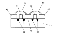
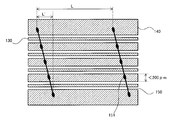
- FIGS. 1 and 2 are a light control element in which two or more signal electrodes (31, 32) are arranged. Proposed bonding the ground electrodes (41, 42, 43) to each other with gold wires (51, 52).
- This proposal has shown that the high-frequency ground potential of the working part is stabilized, crosstalk between the electrodes is suppressed, and stable modulation operation is possible at a wide band frequency.
- FIG. 2 is a cross-sectional view taken along one-dot chain line A-A ′ in FIG. Reference numerals other than those described above indicate the substrate 1, optical waveguides (21 to 23), ground electrodes (44 to 46), and bonding connection lines (53, 54) such as gold wires.
- the bonding part bonds a bonding wire such as gold with ultrasonic waves (thermal ultrasonic pressure bonding) using a needle-shaped bonding tool.
- a thin gold wire generally used is 20 to 30 ⁇ m, and even in that case, a space of about 100 ⁇ m is required as a bonding portion.
- JP 2009-53444 A Japanese Patent No. 5067464
- the problem to be solved by the present invention is to solve the above-described problems and provide a light control element capable of suppressing crosstalk between electrodes even if the light control element is narrowed. It is.
- the light control element of the present invention has the following technical features.
- the modulation electrode includes at least two signals.
- An electrode and a ground electrode arranged so as to sandwich the signal electrode, and the modulation electrode exerting a modulation action on the light wave is disposed between the two signal electrodes.
- the ground electrode is electrically connected to the other ground electrode, and an electrical connection means is provided so as to straddle a part of the signal electrode, and the electrical connection means includes at least A plurality of ground electrodes are connected by a single conductive line.
- the electrical connection means arranges a plurality of the conductive lines, and an interval L between adjacent conductive lines with respect to a direction in which the signal electrode extends. Is set to be less than a quarter of the wavelength ⁇ at the frequency of the modulation signal propagating through the signal electrode.
- the electrical connection means arranges a plurality of the conductive wires, and a distance L between adjacent conductive wires in the direction in which the signal electrode extends. Is set to be less than one-tenth with respect to the wavelength ⁇ at the frequency of the modulation signal propagating through the signal electrode.
- At least a part of a portion where the one conductive wire and the ground electrode are connected is a width of the ground electrode. Is 200 ⁇ m or less.
- the present invention relates to a light control element including a substrate having an electro-optic effect, an optical waveguide formed on the substrate, and a modulation electrode that modulates a light wave propagating through the optical waveguide.
- the modulation electrode includes at least two modulation electrodes. It is composed of a signal electrode and a ground electrode arranged so as to sandwich the signal electrode, and the modulation electrode exerts a modulation action on the light wave, and the modulation electrode is disposed between the two signal electrodes.
- the electrical connecting means arranges a plurality of conductive lines, and the interval L between the conductive lines adjacent to the direction in which the signal electrodes extend propagates through the signal electrodes.
- the distance L between adjacent conductive lines and the length L ′ of each straight line connecting the both ends of the conductive lines with respect to the direction L satisfy the relationship L> L ′.
- the potential between the ground electrodes can be maintained substantially the same, and good signal quality with suppressed crosstalk (for example, variation in frequency characteristics is reduced and stability is increased) is obtained. be able to.
- the above-described length L ′ is also less than a quarter of the wavelength ⁇ , and more preferably one-tenth or less, so that the conductive wire is disposed perpendicular to the direction in which the signal electrode extends. It is possible to suppress crosstalk to the same extent as.
- At least a part of a portion where one conductive line and the ground electrode are connected can achieve a good connection state even when the width of the ground electrode is 200 ⁇ m or less. it can.
- a sufficient connection region can be ensured by arranging the conductive lines obliquely with respect to the direction in which the signal electrodes extend.
- FIG. 10 is a plan view showing an outline of a light control element disclosed in Patent Document 2.
- FIG. FIG. 2 is a cross-sectional view taken along one-dot chain line A-A ′ in FIG. 1. It is a top view concerning the light control element of one mode of the present invention.
- FIG. 4 is a cross-sectional view taken along one-dot chain line AA ′ in FIG. 3. It is the figure which expanded a part of modulation electrode of FIG. It is a figure which shows the other Example of the light control element of 1 aspect of this invention, and is a figure explaining the arrangement
- FIG. 8 is a graph showing the influence of crosstalk when the inclination of the conductive line is changed in the direction in which the signal electrode extends in the light control element of FIG. 7.
- FIG. 3 is a schematic view of a light control element to which the present invention is applied
- FIG. 4 is a cross-sectional view taken along the alternate long and short dash line AA ′ in FIG.
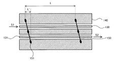
- FIG. 5 is an enlarged view of the modulation electrode portion of FIG.
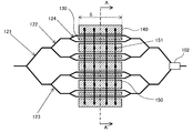
- the light control element of the present invention modulates a substrate 101 having an electro-optic effect, an optical waveguide (121 to 124) formed on the substrate, and a light wave propagating through the optical waveguide.
- the modulation electrode is composed of at least two signal electrodes 130 and a ground electrode 140 disposed so as to sandwich the signal electrode, and the modulation electrode modulates the light wave.
- the working portion S of the modulation electrode is electrically connected to the ground electrode disposed between the two signal electrodes and the other ground electrode, and a part of the signal electrode.
- An electrical connection means arranged so as to straddle is provided, and the electrical connection means is configured to connect at least a plurality of ground electrodes with a single conductive line 150.
- the substrate 1 having an electro-optic effect a single crystal of any one of LiNbO 3 , LiTaO 5 or PLZT (lead lanthanum zirconate titanate) can be suitably used.
- LiNbO 3 and LiTaO 5 frequently used in light control elements such as an optical modulator are preferable.
- the optical waveguide formed on the substrate is formed, for example, by thermally diffusing a high refractive index material such as titanium (Ti) on a LiNbO 3 substrate (LN substrate).
- a ridge-type optical waveguide in which irregularities along the optical waveguide are formed on the substrate can also be used.
- the light control element using the X-cut type substrate is illustrated in FIG. 3, the present invention is not limited to this and can be similarly applied to a Z-cut type substrate.
- FIG. 3 illustrates an optical waveguide used in the DP-QPSK modulator.
- Two second MZ type optical waveguides (122, 123) are inserted into the branching waveguide of the first Mach-Zehnder type optical waveguide (MZ type optical waveguide) 121, and the second MZ type optical waveguide is further branched.
- Four third MZ type optical waveguides 124 are inserted in the waveguide.
- the combining unit 102 of the first MZ type optical waveguide 121 is formed with a polarization combining unit so as to combine two output lights to be combined while changing the polarization plane.
- the light control element of the present invention is not limited to such an optical waveguide, but a crosstalk phenomenon is likely to occur in a light control element having a plurality of light modulation units, and therefore the configuration of the present invention is applied. Superiority.
- the modulation electrode is composed of a signal electrode 130 and a ground electrode 140, and a Ti / Au electrode pattern is formed on the surface of the substrate, and can be formed by a gold plating method or the like. Furthermore, if necessary, a buffer layer such as dielectric SiO 2 can be provided on the surface of the substrate after the optical waveguide is formed, and a modulation electrode can be formed above the buffer layer. It is particularly preferable that the light control element to which the present invention is applied has a configuration in which a ground electrode is disposed between a plurality of signal electrodes.
- a plurality of signal electrodes to which a microwave signal is applied are arranged so that the ground electrode is sandwiched, and the electric field formed by the modulation electrode is applied to the optical waveguide.
- the plurality of ground electrodes are continuously connected (wire bonding) with one conductive wire.
- one conductive wire 250 is used to connect a plurality of ground electrodes 240, and the conductive wires are bonded on each ground electrode 240 with ultrasonic waves.
- a plurality of conductive wires connected in this way are arranged in parallel as necessary.
- the bonding distance required for one ground electrode can be reduced.
- the manufacturing time of the light control element can be shortened.
- the reduction in the number of bondings also reduces damage to the substrate due to bonding.
- the width of the ground electrode sandwiched between the signal electrodes becomes increasingly narrower.
- the present invention can be preferably applied to a case where the width of the ground electrode in the portion to which the conductive line is connected is 200 ⁇ m or less. The reason is that the area required for connection can be minimized by connecting with one conductive line.
- a wider connection area can be secured. Even in a light control element miniaturized by this configuration, the ground potential of the ground electrodes on both sides of the signal electrode is stabilized, crosstalk between the signal electrodes is suppressed, and good modulation signal quality can be obtained.
- a conductive wire having a high conductivity such as a gold wire can be used.
- the conductive wire has as low a loop height as possible (the height of the conductive wire across the signal electrode from the substrate) and the length of the conductive wire is short.
- the length of the conductive wire between the bonding point and the adjacent bonding point is preferably 1 mm or less, more preferably 0.5 mm or less while maintaining a length that does not cause a short between the conductive wire and the signal electrode. Good.
- the interval L between the conductive lines is set to less than a quarter of the wavelength ⁇ at the frequency of the modulation signal propagating through the signal electrode. Also good. With this configuration, it is possible to prevent the electric field from the signal electrode from leaking beyond the ground electrode. More preferably, the crosstalk can be reliably suppressed by setting the interval L to 1/10 or less of the wavelength of the electric signal. In addition, since the electric field formed by the signal electrode is efficiently applied to the optical waveguide, a decrease in modulation efficiency in a wideband frequency is suppressed, and the frequency characteristics can be improved.
- the conductive wire should be perpendicular to the direction in which the signal electricity extends. Need to be placed.
- the length L ′ indicating the inclination of the conductive line with respect to the direction is set to L> L ′, and similarly to the interval L, the length L ′ is set to the wavelength ⁇ at the frequency of the modulation signal propagating through the signal electrode.
- the light control element is usually housed in a metal case and modularized.
- the ground electrode near the side surface of the light control element is connected to the ground side terminal of the signal line introduced from the metal case or the outside.
- the electrical connection means is provided at the action portion where the modulation electrode exerts a modulation action on the light wave. This is because it is necessary to most suppress the crosstalk phenomenon in the action portion. Further, such an action part is present in the vicinity of the center of the substrate of the light control element, and is often located farthest from the place where the ground electrode is grounded to the metal case of the module. For this reason, since it is difficult to ensure a sufficient grounding state, it is necessary to reinforce and stabilize the grounding state using the electrical connection means as in the present invention.
- the signal S1 is input from the left end of the signal electrode 130 and absorbed by the terminator at the right end.
- the left end of the signal electrode 131 is connected to a terminator, and the signal S2 output from the right end is measured. The result is shown in FIG.
Abstract
The purpose of this invention is to provide a light-control element that makes it possible to reduce inter-electrode crosstalk even if the width of said light-control element is reduced. Said light-control element, which has a substrate that exhibits an electro-optic effect, optical waveguides (121 through 124) formed on said substrate, and modulating electrodes that modulate light waves propagating through said optical waveguides, is characterized in that: the modulating electrodes comprise two or more signal electrodes (130) and ground electrodes (140) laid out so as to sandwich said signal electrodes; an acting section (S) of the modulating electrodes, said acting section (S) being the section where the modulating electrodes exert a modulating effect on the light waves, is provided with an electrical connection means that is laid out so as to straddle parts of the signal electrodes and electrically connects the ground electrodes laid out between signal electrodes to the other ground electrodes; and said electrical connection means is designed so as to connect at least a plurality of ground electrodes to each other via a single conductive wire (150).
Description
本発明は、光制御素子に関し、特に、変調電極に2つ以上の信号電極を有する光制御素子に関する。
The present invention relates to a light control element, and more particularly, to a light control element having two or more signal electrodes in a modulation electrode.
ニオブ酸リチウムなどの電気光学効果を有する基板に、光導波路と変調電極を形成し、該光導波路を伝播する光波を該変調電極で変調を光制御素子が実用化されている。近年では、光通信分野などでの通信速度の高速化または通信データの大容量化等のニーズに応えるため、差動四相位相偏移変調(DQPSK変調,Differential Quadrature Phase Shift Keying)方式など複数のマッハツェンダー型光導波路(MZ型光導波路)を複数の変調信号で駆動することが行われている。また、偏波合成を利用したDP-QPSK変調器などコヒーレント多値通信用に複数の信号電極を備えた集積型変調器も利用されている。
An optical control element in which an optical waveguide and a modulation electrode are formed on a substrate having an electro-optic effect such as lithium niobate, and a light wave propagating through the optical waveguide is modulated by the modulation electrode has been put into practical use. In recent years, in order to meet the needs for higher communication speeds and larger communication data capacity in the field of optical communication, etc., there are several methods such as differential quadrature phase shift keying (DQPSK modulation, differential quadrature phase shift keying). A Mach-Zehnder type optical waveguide (MZ type optical waveguide) is driven by a plurality of modulation signals. In addition, an integrated modulator including a plurality of signal electrodes for coherent multilevel communication such as a DP-QPSK modulator using polarization synthesis is also used.
複数の光導波路と複数の信号電極を有している光制御素子においては、各信号電極には異なる変調信号が入力される場合が多く、各々の光導波路に互いに異なる変調信号が印加されるように構成されている。このため、特定の光導波路に予め定められた変調信号以外の電界が作用すると、信号光の消光比などの光制御素子の光学特性が劣化する原因となる。このような現象はクロストークと呼ばれている。
In a light control element having a plurality of optical waveguides and a plurality of signal electrodes, different modulation signals are often inputted to the respective signal electrodes, and different modulation signals are applied to the respective optical waveguides. It is configured. For this reason, when an electric field other than a predetermined modulation signal acts on a specific optical waveguide, optical characteristics of the light control element such as the extinction ratio of the signal light deteriorate. Such a phenomenon is called crosstalk.
電極間のクロストークを抑制するには、光導波路の間隔または電極の間隔を広げることが効果的ではあるが、このような対策は光制御素子のサイズが大きくなる原因となり、好ましくない。また、特許文献1に示すように、光導波路又は信号電極の間に溝を形成する方法も提案されているが、光制御素子の製造工程に溝を設ける工程が別途追加されるので、製造時間及びコストが増加することとなる。また、30μm以下の厚みを有する基板を使用した光制御素子では、溝自体が形成できないか、形成できても基板が破損し易くなるなどの不具合を生じる。
In order to suppress the crosstalk between the electrodes, it is effective to widen the distance between the optical waveguides or the distance between the electrodes, but such a countermeasure is not preferable because it causes the size of the light control element to increase. Also, as shown in Patent Document 1, a method of forming a groove between optical waveguides or signal electrodes has also been proposed, but a process of providing a groove is added to the manufacturing process of the light control element. And the cost will increase. In addition, in the light control element using the substrate having a thickness of 30 μm or less, the groove itself cannot be formed, or even if it can be formed, the substrate is easily damaged.
また、変調信号の周波数が広帯域化するに従い、信号電極を挟む接地電極同士に動作状態に対応した局所的な電位差が発生する。このため、信号電極と該信号電極を挟む接地電極との間に発生する電界の変化が、信号電極の左右で異なる現象が生じる。光導波路にこのような電界が印加されると、意図した変調動作が期待できず、光制御素子の変調特性が大幅に劣化することとなる。
Also, as the frequency of the modulation signal becomes wider, a local potential difference corresponding to the operating state occurs between the ground electrodes that sandwich the signal electrode. For this reason, a phenomenon occurs in which the change in the electric field generated between the signal electrode and the ground electrode sandwiching the signal electrode differs between the left and right sides of the signal electrode. When such an electric field is applied to the optical waveguide, the intended modulation operation cannot be expected, and the modulation characteristics of the light control element will be greatly degraded.
このような問題を解消するため、本出願人は、特許文献2において、図1及び2に示すように、2つ以上の信号電極(31,32)が並んだ光制御素子で、変調作用部に接地電極(41,42,43)同士を金線(51,52)でボンディングすることを提案した。この提案により、作用部の高周波的な接地電位が安定し、電極間のクロストークを抑制し広帯域周波数で安定した変調動作が可能となることを示した。図2は、図1の一点鎖線A-A’における断面図である。上述した以外の各符号は、基板1、光導波路(21~23)、接地電極(44~46)、金線などのボンディング接続線路(53,54)を示す。
In order to solve such a problem, in the patent document 2, the present applicant, as shown in FIGS. 1 and 2, is a light control element in which two or more signal electrodes (31, 32) are arranged. Proposed bonding the ground electrodes (41, 42, 43) to each other with gold wires (51, 52). This proposal has shown that the high-frequency ground potential of the working part is stabilized, crosstalk between the electrodes is suppressed, and stable modulation operation is possible at a wide band frequency. FIG. 2 is a cross-sectional view taken along one-dot chain line A-A ′ in FIG. Reference numerals other than those described above indicate the substrate 1, optical waveguides (21 to 23), ground electrodes (44 to 46), and bonding connection lines (53, 54) such as gold wires.
通常、接地電極の接続にはワイヤーボンディングなどの手段が用いられる。ボンディング部は、金などのボンディング線を、針形状のボンディングツールを用いて、超音波でボンディング(熱超音波圧着)される。一般に用いられる細線の金線は20~30μmであり、その場合でもボンディング部として100μm程度のスペースが必要である。
Usually, means such as wire bonding is used to connect the ground electrode. The bonding part bonds a bonding wire such as gold with ultrasonic waves (thermal ultrasonic pressure bonding) using a needle-shaped bonding tool. A thin gold wire generally used is 20 to 30 μm, and even in that case, a space of about 100 μm is required as a bonding portion.
一方、光制御素子の低コスト化または小型化のためには、光制御素子をより狭幅化する必要がある。そのためには信号電極間隔をより狭くする必要があり、それに応じて信号電極間の接地電極幅がより狭くなり、例えば幅200μm以下のものも用いられる。このような場合に、ボンディング部の位置ずれなどによってボンディング部と信号電極の短絡が発生したり、またはスペース不足でボンディングができないということが発生した。このような問題は,4つのMZ構造が並列するDP-QPSK変調器等の高集積化した光制御素子ではより顕著となる。
On the other hand, in order to reduce the cost or size of the light control element, it is necessary to narrow the width of the light control element. For this purpose, it is necessary to make the interval between the signal electrodes narrower, and accordingly, the width of the ground electrode between the signal electrodes becomes narrower. In such a case, a short circuit between the bonding part and the signal electrode may occur due to a positional deviation of the bonding part, or bonding may not be possible due to insufficient space. Such a problem becomes more conspicuous in a highly integrated light control element such as a DP-QPSK modulator in which four MZ structures are arranged in parallel.
本発明が解決しようとする課題は、上述したような問題を解決し、光制御素子の狭幅化を行っても、電極間のクロストークを抑制することが可能な光制御素子を提供することである。
The problem to be solved by the present invention is to solve the above-described problems and provide a light control element capable of suppressing crosstalk between electrodes even if the light control element is narrowed. It is.
上記課題を解決するため、本発明の光制御素子は以下のような技術的特徴を有する。
(1) 電気光学効果を有する基板と、該基板に形成された光導波路と、該光導波路を伝播する光波を変調する変調電極とを有する光制御素子において、該変調電極は、少なくとも二つの信号電極と該信号電極を挟むように配置された接地電極から構成され、該変調電極が該光波に変調作用を及ぼしている該変調電極の作用部分には、二つの該信号電極の間に配置された該接地電極と、それ以外の該接地電極とを電気的に接続すると共に、該信号電極の一部を跨ぐように配置された電気的接続手段が設けられ、該電気的接続手段は、少なくとも複数の接地電極の間を1本の導電線で接続するよう構成されていることを特徴とする。 In order to solve the above problems, the light control element of the present invention has the following technical features.
(1) In a light control element having a substrate having an electro-optic effect, an optical waveguide formed on the substrate, and a modulation electrode that modulates a light wave propagating through the optical waveguide, the modulation electrode includes at least two signals. An electrode and a ground electrode arranged so as to sandwich the signal electrode, and the modulation electrode exerting a modulation action on the light wave is disposed between the two signal electrodes. The ground electrode is electrically connected to the other ground electrode, and an electrical connection means is provided so as to straddle a part of the signal electrode, and the electrical connection means includes at least A plurality of ground electrodes are connected by a single conductive line.
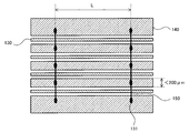
(2) 上記(1)に記載の光制御素子において、該電気的接続手段は、該導電線を複数本並べて配置し、該信号電極が延在する方向に対して隣接する導電線の間隔Lは、該信号電極を伝搬する変調信号の周波数における波長λに対し、4分の1未満となるように設定されていることを特徴とする。
(2) In the light control element according to the above (1), the electrical connection means arranges a plurality of the conductive lines, and an interval L between adjacent conductive lines with respect to a direction in which the signal electrode extends. Is set to be less than a quarter of the wavelength λ at the frequency of the modulation signal propagating through the signal electrode.
(3) 上記(1)に記載の光制御素子において、該電気的接続手段は、該導電線を複数本並べて配置し、該信号電極が延在する方向に対して隣接する導電線の間隔Lは、該信号電極を伝搬する変調信号の周波数における波長λに対し、10分の1未満となるように設定されていることを特徴とする。
(3) In the light control element according to the above (1), the electrical connection means arranges a plurality of the conductive wires, and a distance L between adjacent conductive wires in the direction in which the signal electrode extends. Is set to be less than one-tenth with respect to the wavelength λ at the frequency of the modulation signal propagating through the signal electrode.
(4) 上記(2)又は(3)に記載の光制御素子において、前記隣接する導電線の間隔Lと、各導電線が該方向に対し斜めに配置され、導電線の両端部を結ぶ直線の該方向に対する長さL’とが、L>L’の関係を満足することを特徴とする。
(4) In the light control element according to the above (2) or (3), the interval L between the adjacent conductive lines and a straight line connecting the both ends of the conductive lines, with each conductive line being disposed obliquely with respect to the direction. The length L ′ in the direction satisfies the relationship L> L ′.
(5) 上記(1)乃至(4)のいずれかに記載の光制御素子において、前記1本の導電線と該接地電極とが接続されている部分の少なくとも一部は、該接地電極の幅が200μm以下であることを特徴とする。
(5) In the light control element according to any one of (1) to (4), at least a part of a portion where the one conductive wire and the ground electrode are connected is a width of the ground electrode. Is 200 μm or less.
(5) In the light control element according to any one of (1) to (4), at least a part of a portion where the one conductive wire and the ground electrode are connected is a width of the ground electrode. Is 200 μm or less.
本発明は、電気光学効果を有する基板と、該基板に形成された光導波路と、該光導波路を伝播する光波を変調する変調電極とを有する光制御素子において、該変調電極は、少なくとも二つの信号電極と該信号電極を挟むように配置された接地電極から構成され、該変調電極が該光波に変調作用を及ぼしている該変調電極の作用部分には、二つの該信号電極の間に配置された該接地電極と、それ以外の該接地電極とを電気的に接続すると共に、該信号電極の一部を跨ぐように配置された電気的接続手段が設けられ、該電気的接続手段は、少なくとも複数の接地電極の間を1本の導電線で接続するよう構成されているので、接地電極の幅が狭い場合でも、導電線のボンディングが可能となる。しかも、信号電極を跨ぐ箇所毎に導電線の両端を接地電極にボンディングする方法と比較し、本発明ではボンディング箇所を大幅に減らすことも可能となる。
The present invention relates to a light control element including a substrate having an electro-optic effect, an optical waveguide formed on the substrate, and a modulation electrode that modulates a light wave propagating through the optical waveguide. The modulation electrode includes at least two modulation electrodes. It is composed of a signal electrode and a ground electrode arranged so as to sandwich the signal electrode, and the modulation electrode exerts a modulation action on the light wave, and the modulation electrode is disposed between the two signal electrodes. Electrically connecting means arranged so as to straddle part of the signal electrode, and electrically connecting the grounded electrode and the other grounded electrode, and the electrical connecting means, Since at least a plurality of ground electrodes are connected by a single conductive line, the conductive lines can be bonded even when the width of the ground electrode is narrow. In addition, compared with a method in which both ends of the conductive wire are bonded to the ground electrode at each location straddling the signal electrode, the number of bonding locations can be greatly reduced in the present invention.
また、本発明の光制御素子では、電気的接続手段は、導電線を複数本並べて配置し、信号電極が延在する方向に対して隣接する導電線の間隔Lは、該信号電極を伝搬する変調信号の周波数における波長λに対し、4分の1未満、より好ましくは10分の1以下となるように設定することで、信号電極間のクロストークを効率良く抑制することが可能となる。その結果、周波数特性自体が改善する。
In the light control element of the present invention, the electrical connecting means arranges a plurality of conductive lines, and the interval L between the conductive lines adjacent to the direction in which the signal electrodes extend propagates through the signal electrodes. By setting the wavelength λ at the frequency of the modulation signal to be less than one quarter, more preferably one tenth or less, crosstalk between signal electrodes can be efficiently suppressed. As a result, the frequency characteristic itself is improved.
さらに、隣接する導電線の間隔Lと、各導電線が該方向に対し斜めに配置され、導電線の両端部を結ぶ直線の該方向に対する長さL’とが、L>L’の関係を満足するよう設定することで、接地電極間の電位をほぼ同じに維持することができ、クロストークを抑制した良好な信号品質(例えば、周波数特性に関しバラツキが小さくなり安定性が増すこと)を得ることができる。
なお、上述した長さL’についても同様に、波長λの4分の1未満、より好ましくは10分の1以下とすることで、信号電極が延在する方向に垂直に配置される導電線と同等程度に、クロストークを抑制することが可能となる。 Furthermore, the distance L between adjacent conductive lines and the length L ′ of each straight line connecting the both ends of the conductive lines with respect to the direction L satisfy the relationship L> L ′. By setting so as to satisfy, the potential between the ground electrodes can be maintained substantially the same, and good signal quality with suppressed crosstalk (for example, variation in frequency characteristics is reduced and stability is increased) is obtained. be able to.
Similarly, the above-described length L ′ is also less than a quarter of the wavelength λ, and more preferably one-tenth or less, so that the conductive wire is disposed perpendicular to the direction in which the signal electrode extends. It is possible to suppress crosstalk to the same extent as.
また、本発明の光制御素子では、1本の導電線と接地電極とが接続されている部分の少なくとも一部は、該接地電極の幅が200μm以下であっても、良好な接続状態を達成できる。特に、信号電極が延在する方向に対して導電線を斜めに配置することにより、十分な接続領域を確保することができる。
In the light control element of the present invention, at least a part of a portion where one conductive line and the ground electrode are connected can achieve a good connection state even when the width of the ground electrode is 200 μm or less. it can. In particular, a sufficient connection region can be ensured by arranging the conductive lines obliquely with respect to the direction in which the signal electrodes extend.
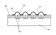
以下、本発明の光制御素子について、好適例を用いて詳細に説明する。図3は本発明が適用される光制御素子の概略図であり、図4は、図3における一点鎖線A-A’における断面図である。また、図5は、図3の変調電極部分の拡大図である。
本発明の光制御素子は、図3乃至5に示すように、電気光学効果を有する基板101と、該基板に形成された光導波路(121~124)と、該光導波路を伝播する光波を変調する変調電極とを有する光制御素子において、該変調電極は、少なくとも二つの信号電極130と該信号電極を挟むように配置された接地電極140から構成され、該変調電極が該光波に変調作用を及ぼしている該変調電極の作用部分Sには、二つの該信号電極の間に配置された該接地電極と、それ以外の該接地電極とを電気的に接続すると共に、該信号電極の一部を跨ぐように配置された電気的接続手段が設けられ、該電気的接続手段は、少なくとも複数の接地電極の間を1本の導電線150で接続するよう構成されていることを特徴とする。 Hereinafter, the light control element of the present invention will be described in detail using preferred examples. FIG. 3 is a schematic view of a light control element to which the present invention is applied, and FIG. 4 is a cross-sectional view taken along the alternate long and short dash line AA ′ in FIG. FIG. 5 is an enlarged view of the modulation electrode portion of FIG.
As shown in FIGS. 3 to 5, the light control element of the present invention modulates asubstrate 101 having an electro-optic effect, an optical waveguide (121 to 124) formed on the substrate, and a light wave propagating through the optical waveguide. In the light control element having the modulation electrode, the modulation electrode is composed of at least two signal electrodes 130 and a ground electrode 140 disposed so as to sandwich the signal electrode, and the modulation electrode modulates the light wave. The working portion S of the modulation electrode is electrically connected to the ground electrode disposed between the two signal electrodes and the other ground electrode, and a part of the signal electrode. An electrical connection means arranged so as to straddle is provided, and the electrical connection means is configured to connect at least a plurality of ground electrodes with a single conductive line 150.
本発明の光制御素子は、図3乃至5に示すように、電気光学効果を有する基板101と、該基板に形成された光導波路(121~124)と、該光導波路を伝播する光波を変調する変調電極とを有する光制御素子において、該変調電極は、少なくとも二つの信号電極130と該信号電極を挟むように配置された接地電極140から構成され、該変調電極が該光波に変調作用を及ぼしている該変調電極の作用部分Sには、二つの該信号電極の間に配置された該接地電極と、それ以外の該接地電極とを電気的に接続すると共に、該信号電極の一部を跨ぐように配置された電気的接続手段が設けられ、該電気的接続手段は、少なくとも複数の接地電極の間を1本の導電線150で接続するよう構成されていることを特徴とする。 Hereinafter, the light control element of the present invention will be described in detail using preferred examples. FIG. 3 is a schematic view of a light control element to which the present invention is applied, and FIG. 4 is a cross-sectional view taken along the alternate long and short dash line AA ′ in FIG. FIG. 5 is an enlarged view of the modulation electrode portion of FIG.
As shown in FIGS. 3 to 5, the light control element of the present invention modulates a
電気光学効果を有する基板1としては、特に、LiNbO3,LiTaO5又はPLZT(ジルコン酸チタン酸鉛ランタン)のいずれかの単結晶が好適に利用可能である。特に、光変調器などの光制御素子で多用されているLiNbO3,LiTaO5が、好ましい。また、基板に形成する光導波路は、例えば、LiNbO3基板(LN基板)上にチタン(Ti)などの高屈折率物質を熱拡散することにより形成される。また、基板に光導波路に沿った凹凸を形成したリッジ型光導波路も利用可能である。さらに、図3では、Xカット型の基板を用いた光制御素子を例示しているが、本発明はこれに限らずZカット型の基板でも同様に適用することが可能である。
As the substrate 1 having an electro-optic effect, a single crystal of any one of LiNbO 3 , LiTaO 5 or PLZT (lead lanthanum zirconate titanate) can be suitably used. In particular, LiNbO 3 and LiTaO 5 frequently used in light control elements such as an optical modulator are preferable. The optical waveguide formed on the substrate is formed, for example, by thermally diffusing a high refractive index material such as titanium (Ti) on a LiNbO 3 substrate (LN substrate). A ridge-type optical waveguide in which irregularities along the optical waveguide are formed on the substrate can also be used. Further, although the light control element using the X-cut type substrate is illustrated in FIG. 3, the present invention is not limited to this and can be similarly applied to a Z-cut type substrate.
図3はDP-QPSK変調器に使用される光導波路を例示している。第1のマッハツェンダー型光導波路(MZ型光導波路)121の分岐導波路に、2つの第2のMZ型光導波路(122,123)が挿入され、さらに、第2のMZ型光導波路の分岐導波路に4つの第3のMZ型光導波路124が挿入されている。第1のMZ型光導波路121の合波部102には、合波する2つの出力光を偏波面を変えて合成するように、偏波合成部が形成されている。本発明の光制御素子はこのような光導波路に限定されるものではないが、複数の光変調部を有する光制御素子においては、クロストーク現象が発生し易いので、本発明の構成を適用する優位性が高い。
FIG. 3 illustrates an optical waveguide used in the DP-QPSK modulator. Two second MZ type optical waveguides (122, 123) are inserted into the branching waveguide of the first Mach-Zehnder type optical waveguide (MZ type optical waveguide) 121, and the second MZ type optical waveguide is further branched. Four third MZ type optical waveguides 124 are inserted in the waveguide. The combining unit 102 of the first MZ type optical waveguide 121 is formed with a polarization combining unit so as to combine two output lights to be combined while changing the polarization plane. The light control element of the present invention is not limited to such an optical waveguide, but a crosstalk phenomenon is likely to occur in a light control element having a plurality of light modulation units, and therefore the configuration of the present invention is applied. Superiority.
変調電極は、信号電極130と接地電極140から構成され、基板表面に、Ti・Auの電極パターンを形成し、金メッキ方法などにより形成することが可能である。さらに、必要に応じて光導波路形成後の基板表面に誘電体SiO2等のバッファ層を設け、該バッファ層の上側に変調電極を形成することも可能である。本発明が適用される光制御素子は、複数の信号電極の間にも接地電極が配置された構成を有するものが、特に好ましい。
The modulation electrode is composed of a signal electrode 130 and a ground electrode 140, and a Ti / Au electrode pattern is formed on the surface of the substrate, and can be formed by a gold plating method or the like. Furthermore, if necessary, a buffer layer such as dielectric SiO 2 can be provided on the surface of the substrate after the optical waveguide is formed, and a modulation electrode can be formed above the buffer layer. It is particularly preferable that the light control element to which the present invention is applied has a configuration in which a ground electrode is disposed between a plurality of signal electrodes.
本発明の光制御素子では、マイクロ波信号が印加される複数の信号電極を接地電極が挟むように配置されており、変調電極が形成する電界が光導波路に印加されている変調電極の作用部分で、前記複数の接地電極を、1本の導電線で連続して接続(ワイヤーボンディング)することを特徴としている。図3又は図5に示すように、複数の接地電極240を接続するのに、1本の導電線250が使用され、各接地電極240上で導電線が超音波でボンディングされている。このように接続した導電線を必要に応じて複数本を並列に配置するよう構成している。
In the light control element of the present invention, a plurality of signal electrodes to which a microwave signal is applied are arranged so that the ground electrode is sandwiched, and the electric field formed by the modulation electrode is applied to the optical waveguide. Thus, the plurality of ground electrodes are continuously connected (wire bonding) with one conductive wire. As shown in FIG. 3 or FIG. 5, one conductive wire 250 is used to connect a plurality of ground electrodes 240, and the conductive wires are bonded on each ground electrode 240 with ultrasonic waves. A plurality of conductive wires connected in this way are arranged in parallel as necessary.
1本の導電線で複数(少なくとも3つ以上)の接地電極を連続ボンディングすることにより、1つの接地電極に必要なボンディング距離が小さくすることができる。しかも、ボンディング数が少なくなることで、光制御素子の製造時間を短縮することができる。さらには、基板が数十μm程度の薄板を用いる場合には、ボンディング回数の低減は、ボンディングによる基板へのダメージを軽減することにもなる。
By continuously bonding a plurality of (at least three or more) ground electrodes with one conductive wire, the bonding distance required for one ground electrode can be reduced. In addition, since the number of bondings is reduced, the manufacturing time of the light control element can be shortened. Furthermore, when a thin plate having a thickness of about several tens of μm is used, the reduction in the number of bondings also reduces damage to the substrate due to bonding.
光制御素子の狭幅化に伴い、信号電極に挟まれる接地電極の幅はますます狭くなる。特に、導電線が接続される部分の接地電極の幅が200μm以下である場合に対しても、本発明は好適に適用することができる。その理由は、1本の導電線による接続で接続に必要な領域を最小化できることによる。また、図6に示すように、ボンディング方向(導電線の長手方向)を信号電極が延在する方向に対して傾斜させることにより、接続部分の領域をより広く確保することができる。この構成により小型化した光制御素子でも、信号電極の両側の接地電極の接地電位が安定し,信号電極間のクロストークが抑制され、良好な変調信号品質をえることができる。
As the light control element becomes narrower, the width of the ground electrode sandwiched between the signal electrodes becomes increasingly narrower. In particular, the present invention can be preferably applied to a case where the width of the ground electrode in the portion to which the conductive line is connected is 200 μm or less. The reason is that the area required for connection can be minimized by connecting with one conductive line. In addition, as shown in FIG. 6, by widening the bonding direction (longitudinal direction of the conductive wire) with respect to the direction in which the signal electrode extends, a wider connection area can be secured. Even in a light control element miniaturized by this configuration, the ground potential of the ground electrodes on both sides of the signal electrode is stabilized, crosstalk between the signal electrodes is suppressed, and good modulation signal quality can be obtained.
本発明の光制御素子に用いられる電気的接続手段としては、金線などの導電率の高い導電線が利用可能である。接地電極間に高周波的な電位差を生じさせないためには、導電線の抵抗性分とインダクタンス成分を小さくする必要がある。このため導電線は、できる限りループ高さ(信号電極を跨ぐ導電線の基板からの高さ)が低く、導電線の長さが短いことが望ましい。そのためには、好ましくはボンディング点と隣接するボンディング点との間における導電線の長さが、導電線と信号電極とがショートしない長さを保ちつつ、1mm以下、更に好ましくは0.5mm以下にすると良い。
As the electrical connection means used in the light control element of the present invention, a conductive wire having a high conductivity such as a gold wire can be used. In order to prevent a high-frequency potential difference between the ground electrodes, it is necessary to reduce the resistance component and the inductance component of the conductive wire. For this reason, it is desirable that the conductive wire has as low a loop height as possible (the height of the conductive wire across the signal electrode from the substrate) and the length of the conductive wire is short. For this purpose, the length of the conductive wire between the bonding point and the adjacent bonding point is preferably 1 mm or less, more preferably 0.5 mm or less while maintaining a length that does not cause a short between the conductive wire and the signal electrode. Good.
図5及び6に示すように、導電線を複数配置する際には、導電線の間隔Lは、信号電極を伝搬する変調信号の周波数における波長λに対し、4分の1未満に設定してもよい。この構成により、信号電極からの電界が接地電極を超えて漏れ出すことを抑制することが可能となる。より好ましくは、間隔Lを電気信号の波長の10分の1以下に設定することで、確実にクロストークを抑制することが可能となる。しかも、信号電極が形成する電界が効率良く光導波路に印加されるので、広帯域周波数における変調効率の低下も抑制され、周波数特性を改善することが可能となる。
As shown in FIGS. 5 and 6, when a plurality of conductive lines are arranged, the interval L between the conductive lines is set to less than a quarter of the wavelength λ at the frequency of the modulation signal propagating through the signal electrode. Also good. With this configuration, it is possible to prevent the electric field from the signal electrode from leaking beyond the ground electrode. More preferably, the crosstalk can be reliably suppressed by setting the interval L to 1/10 or less of the wavelength of the electric signal. In addition, since the electric field formed by the signal electrode is efficiently applied to the optical waveguide, a decrease in modulation efficiency in a wideband frequency is suppressed, and the frequency characteristics can be improved.
図6のように、信号電極が延在している方向に対して導電線の長手方向を傾斜させる場合には、信号電極が延在している方向に対して隣接する導電線の間隔Lと、各導電線の両端部を結ぶ直線の該方向(信号電極が延在している方向)に対する長さ(投影した長さ)L’とが、次の関係式を満足するように設定してもよい。
(関係式) L>L’ As shown in FIG. 6, when the longitudinal direction of the conductive line is inclined with respect to the direction in which the signal electrode extends, the distance L between adjacent conductive lines with respect to the direction in which the signal electrode extends The length (projected length) L ′ with respect to the direction (direction in which the signal electrode extends) of the straight line connecting both ends of each conductive line is set so as to satisfy the following relational expression: Also good.
(Relational expression) L> L '
上記長さL’が上記間隔Lより大きくなると、接地電極同士に電位差が発生し、信号電極の左右で接地電極との間に形成される電界に差が生じるなどの不具合が発生する。特に、導電線が複数本並列して配置されている場合には、図6の最上端の接地電極と最下端の接地電極とでは、L≦L’となる場合には、電位変動に大きな位相差が発生し、光制御素子の変調特性が大幅に劣化することとなる。
When the length L ′ is larger than the interval L, a potential difference is generated between the ground electrodes, and a problem such as a difference in electric field formed between the signal electrode and the ground electrode occurs. In particular, when a plurality of conductive lines are arranged in parallel, when L ≦ L ′ between the uppermost ground electrode and the lowermost ground electrode in FIG. A phase difference occurs, and the modulation characteristics of the light control element are greatly deteriorated.
上記長さL’については、信号電極の左右の接地電極間で同電位となるようにするには、図5のように、信号電が延在する方向に対し垂直となるように導電線を配置する必要がある。この構成に近づけるため、前記方向に対する導電線の傾きを示す該長さL’は、L>L’とし、さらに、上記間隔Lと同様に、信号電極を伝搬する変調信号の周波数における波長λに対し、4分の1未満、より好ましくは10分の1以下とすることが望ましい。これらの構成により、周波数特性のバラツキを小さくし、安定性を増加させることが可能となる。
For the length L ′, in order to have the same potential between the left and right ground electrodes of the signal electrode, as shown in FIG. 5, the conductive wire should be perpendicular to the direction in which the signal electricity extends. Need to be placed. In order to approximate this configuration, the length L ′ indicating the inclination of the conductive line with respect to the direction is set to L> L ′, and similarly to the interval L, the length L ′ is set to the wavelength λ at the frequency of the modulation signal propagating through the signal electrode. On the other hand, it is desirable to set it to less than one quarter, more preferably one tenth or less. With these configurations, it is possible to reduce the variation in frequency characteristics and increase the stability.
光制御素子は、通常、金属ケースに収納されモジュール化されることが多い。このような場合には、光制御素子の側面付近の接地電極は、金属ケース又は外部から導入される信号線の接地側端子に接続されている。
The light control element is usually housed in a metal case and modularized. In such a case, the ground electrode near the side surface of the light control element is connected to the ground side terminal of the signal line introduced from the metal case or the outside.
また、上述したように、電気的接続手段は、変調電極が光波に変調作用を及ぼしている作用部分に設けることが好ましい。これは、作用部分におけるクロストーク現象を最も抑制することが必要であるためである。また、このような作用部分は、光制御素子の基板の中央付近に存在し、接地電極がモジュールの金属ケースなどに接地される場所から最も遠い場所にある場合が多い。このため、十分な接地状態を確保し難いので、本発明のような電気的接続手段を用いて接地状態を強化・安定化することが必要である。
Also, as described above, it is preferable that the electrical connection means is provided at the action portion where the modulation electrode exerts a modulation action on the light wave. This is because it is necessary to most suppress the crosstalk phenomenon in the action portion. Further, such an action part is present in the vicinity of the center of the substrate of the light control element, and is often located farthest from the place where the ground electrode is grounded to the metal case of the module. For this reason, since it is difficult to ensure a sufficient grounding state, it is necessary to reinforce and stabilize the grounding state using the electrical connection means as in the present invention.
次に、2つのMZ型光導波路を並列に配置した場合のクロストークの影響(2×2ポートの電極のクロストーク特性)を調べた。図7に示すように、一方のMZ型光導波路(不図示)に沿って配置された信号電極130と他方のMZ型光導波路(不図示)に沿って配置された信号電極131とのクロストーク特性を測定する。
Next, the influence of crosstalk when two MZ type optical waveguides are arranged in parallel (crosstalk characteristics of a 2 × 2 port electrode) was examined. As shown in FIG. 7, the crosstalk between the signal electrode 130 arranged along one MZ type optical waveguide (not shown) and the signal electrode 131 arranged along the other MZ type optical waveguide (not shown). Measure characteristics.
信号電極130の左端より信号S1を入力し、右端で終端器に吸収させる。他方、信号電極131の左端は終端器に接続し、右端から出力される信号S2を測定する。その結果を図8に示す。
The signal S1 is input from the left end of the signal electrode 130 and absorbed by the terminator at the right end. On the other hand, the left end of the signal electrode 131 is connected to a terminator, and the signal S2 output from the right end is measured. The result is shown in FIG.
導電線150が信号電極の延在する方向に垂直な場合(L’=0)が最も良好な特性を発揮する。これに近い良好な結果を示すのが、L’/L=0.08(垂直に対する傾きは約4.5度)の場合である。L’/L=0.7(垂直に対する傾きは約35度)の場合は周波数が広帯域になるに従い、特性の劣化が顕著となっているのが分かる。
When the conductive wire 150 is perpendicular to the direction in which the signal electrode extends (L ′ = 0), the best characteristics are exhibited. A good result close to this is shown when L ′ / L = 0.08 (the inclination with respect to the vertical is about 4.5 degrees). In the case of L '/ L = 0.7 (the inclination with respect to the vertical is about 35 degrees), it can be seen that the deterioration of the characteristics becomes more remarkable as the frequency becomes wider.
以上説明したように、本発明によれば、光制御素子の狭幅化を行っても、電極間のクロストークを抑制することが可能な光制御素子を提供することができる。
As described above, according to the present invention, it is possible to provide a light control element capable of suppressing crosstalk between electrodes even if the light control element is narrowed.
1,101,201 基板
21~23,121~124 光導波路
31,32,130,131 信号電極
41~47,140 接地電極
51~54,150 導電線
151 ボンディング場所 1, 101, 201 Substrate 21-23, 121- 124 Optical waveguide 31, 32, 130, 131 Signal electrode 41-47, 140 Ground electrode 51-54, 150 Conductive line 151 Bonding location
21~23,121~124 光導波路
31,32,130,131 信号電極
41~47,140 接地電極
51~54,150 導電線
151 ボンディング場所 1, 101, 201 Substrate 21-23, 121-
Claims (5)
- 電気光学効果を有する基板と、該基板に形成された光導波路と、該光導波路を伝播する光波を変調する変調電極とを有する光制御素子において、
該変調電極は、少なくとも二つの信号電極と該信号電極を挟むように配置された接地電極から構成され、
該変調電極が該光波に変調作用を及ぼしている該変調電極の作用部分には、二つの該信号電極の間に配置された該接地電極と、それ以外の該接地電極とを電気的に接続すると共に、該信号電極の一部を跨ぐように配置された電気的接続手段が設けられ、
該電気的接続手段は、少なくとも複数の接地電極の間を1本の導電線で接続するよう構成されていることを特徴とする光制御素子。 In a light control element having a substrate having an electro-optic effect, an optical waveguide formed on the substrate, and a modulation electrode that modulates a light wave propagating through the optical waveguide,
The modulation electrode is composed of at least two signal electrodes and a ground electrode arranged so as to sandwich the signal electrode,
The ground electrode arranged between the two signal electrodes and the other ground electrode are electrically connected to the working portion of the modulation electrode where the modulation electrode exerts a modulation action on the light wave And electrical connection means arranged so as to straddle part of the signal electrode,
The light control element is configured so that at least a plurality of ground electrodes are connected by a single conductive line. - 請求項1に記載の光制御素子において、該電気的接続手段は、該導電線を複数本並べて配置し、該信号電極が延在する方向に対して隣接する導電線の間隔Lは、該信号電極を伝搬する変調信号の周波数における波長λに対し、4分の1未満となるように設定されていることを特徴とする光制御素子。 2. The light control element according to claim 1, wherein the electrical connection unit includes a plurality of the conductive lines arranged side by side, and a distance L between adjacent conductive lines with respect to a direction in which the signal electrode extends is defined by the signal control signal. A light control element, wherein the light control element is set to be less than a quarter of a wavelength λ at a frequency of a modulation signal propagating through an electrode.
- 請求項1に記載の光制御素子において、該電気的接続手段は、該導電線を複数本並べて配置し、該信号電極が延在する方向に対して隣接する導電線の間隔Lは、該信号電極を伝搬する変調信号の周波数における波長λに対し、10分の1未満となるように設定されていることを特徴とする光制御素子。 2. The light control element according to claim 1, wherein the electrical connection unit includes a plurality of the conductive lines arranged side by side, and a distance L between adjacent conductive lines with respect to a direction in which the signal electrode extends is defined by the signal control signal. A light control element, wherein the light control element is set to be less than one-tenth with respect to a wavelength λ at a frequency of a modulation signal propagating through an electrode.
- 請求項2又は3に記載の光制御素子において、前記隣接する導電線の間隔Lと、各導電線が該方向に対し斜めに配置され、導電線の両端部を結ぶ直線の該方向に対する長さL’とが、L>L’の関係を満足することを特徴とする光制御素子。 4. The light control element according to claim 2, wherein an interval L between the adjacent conductive lines and a length of the straight line connecting the both ends of the conductive line with respect to the direction are arranged obliquely with respect to the direction. L ′ satisfies the relationship L> L ′ with respect to L ′.
- 請求項1乃至4のいずれかに記載の光制御素子において、前記1本の導電線と該接地電極とが接続されている部分の少なくとも一部は、該接地電極の幅が200μm以下であることを特徴とする光制御素子。 5. The light control element according to claim 1, wherein at least a part of a portion where the one conductive wire and the ground electrode are connected has a width of the ground electrode of 200 μm or less. A light control element characterized by the above.
Applications Claiming Priority (2)
| Application Number | Priority Date | Filing Date | Title |
|---|---|---|---|
| JP2014073504A JP5991339B2 (en) | 2014-03-31 | 2014-03-31 | Light control element |
| JP2014-073504 | 2014-03-31 |
Publications (1)
| Publication Number | Publication Date |
|---|---|
| WO2015151978A1 true WO2015151978A1 (en) | 2015-10-08 |
Family
ID=54240304
Family Applications (1)
| Application Number | Title | Priority Date | Filing Date |
|---|---|---|---|
| PCT/JP2015/059234 WO2015151978A1 (en) | 2014-03-31 | 2015-03-25 | Light-control element |
Country Status (2)
| Country | Link |
|---|---|
| JP (1) | JP5991339B2 (en) |
| WO (1) | WO2015151978A1 (en) |
Cited By (5)
| Publication number | Priority date | Publication date | Assignee | Title |
|---|---|---|---|---|
| WO2018002658A1 (en) * | 2016-07-01 | 2018-01-04 | Oclaro Technology Limited | Ground structure in rf waveguide array |
| EP3432059A4 (en) * | 2016-03-18 | 2019-10-30 | Nippon Telegraph and Telephone Corporation | Optical modulator |
| EP3432058A4 (en) * | 2016-03-18 | 2019-11-06 | Nippon Telegraph And Telephone Corporation | Optical modulator |
| US10678114B2 (en) | 2016-07-01 | 2020-06-09 | Lumentum Technology Uk Limited | Ground structure in RF waveguide array |
| CN111936919A (en) * | 2018-03-30 | 2020-11-13 | 住友大阪水泥株式会社 | Optical waveguide element |
Families Citing this family (3)
| Publication number | Priority date | Publication date | Assignee | Title |
|---|---|---|---|---|
| JP6603571B2 (en) * | 2015-12-17 | 2019-11-06 | 日本電信電話株式会社 | Light modulator |
| JP7052444B2 (en) * | 2018-03-15 | 2022-04-12 | 住友大阪セメント株式会社 | Optical modulators and optical transmission devices |
| JP7283180B2 (en) | 2019-03-29 | 2023-05-30 | 住友大阪セメント株式会社 | optical modulator |
Citations (4)
| Publication number | Priority date | Publication date | Assignee | Title |
|---|---|---|---|---|
| US6192167B1 (en) * | 1998-07-24 | 2001-02-20 | Uniphase Telecommunications Products | Differential drive optical modulator |
| US20030228081A1 (en) * | 2002-05-02 | 2003-12-11 | Tavlykaev Robert F. | Optical modulators with coplanar-waveguide-to-coplanar-strip electrode transitions |
| JP2012078496A (en) * | 2010-09-30 | 2012-04-19 | Sumitomo Osaka Cement Co Ltd | Optical control element |
| JP2012163882A (en) * | 2011-02-09 | 2012-08-30 | Anritsu Corp | Optical modulator |
-
2014
- 2014-03-31 JP JP2014073504A patent/JP5991339B2/en active Active
-
2015
- 2015-03-25 WO PCT/JP2015/059234 patent/WO2015151978A1/en active Application Filing
Patent Citations (4)
| Publication number | Priority date | Publication date | Assignee | Title |
|---|---|---|---|---|
| US6192167B1 (en) * | 1998-07-24 | 2001-02-20 | Uniphase Telecommunications Products | Differential drive optical modulator |
| US20030228081A1 (en) * | 2002-05-02 | 2003-12-11 | Tavlykaev Robert F. | Optical modulators with coplanar-waveguide-to-coplanar-strip electrode transitions |
| JP2012078496A (en) * | 2010-09-30 | 2012-04-19 | Sumitomo Osaka Cement Co Ltd | Optical control element |
| JP2012163882A (en) * | 2011-02-09 | 2012-08-30 | Anritsu Corp | Optical modulator |
Cited By (9)
| Publication number | Priority date | Publication date | Assignee | Title |
|---|---|---|---|---|
| EP3432059A4 (en) * | 2016-03-18 | 2019-10-30 | Nippon Telegraph and Telephone Corporation | Optical modulator |
| EP3432058A4 (en) * | 2016-03-18 | 2019-11-06 | Nippon Telegraph And Telephone Corporation | Optical modulator |
| US10852618B2 (en) | 2016-03-18 | 2020-12-01 | Nippon Telegraph And Telephone Corporation | Optical modulator having interconnecting ground electrodes for coplanar waveguides |
| US10890787B2 (en) | 2016-03-18 | 2021-01-12 | Nippon Telegraph And Telephone Corporation | Optical modulator |
| WO2018002658A1 (en) * | 2016-07-01 | 2018-01-04 | Oclaro Technology Limited | Ground structure in rf waveguide array |
| US10678114B2 (en) | 2016-07-01 | 2020-06-09 | Lumentum Technology Uk Limited | Ground structure in RF waveguide array |
| US10684528B2 (en) | 2016-07-01 | 2020-06-16 | Lumentum Technology Uk Limited | Ground structure in RF waveguide array |
| CN111936919A (en) * | 2018-03-30 | 2020-11-13 | 住友大阪水泥株式会社 | Optical waveguide element |
| CN111936919B (en) * | 2018-03-30 | 2024-01-02 | 住友大阪水泥株式会社 | Optical waveguide element |
Also Published As
| Publication number | Publication date |
|---|---|
| JP2015197452A (en) | 2015-11-09 |
| JP5991339B2 (en) | 2016-09-14 |
Similar Documents
| Publication | Publication Date | Title |
|---|---|---|
| JP5991339B2 (en) | Light control element | |
| JP5067464B2 (en) | Light control element | |
| US7643708B2 (en) | Optical modulator | |
| US8135242B2 (en) | Optical modulator | |
| JP4899730B2 (en) | Light modulator | |
| US10228605B2 (en) | Waveguide optical element | |
| US7869669B2 (en) | Optical phase modulator | |
| JP2008089936A (en) | Optical control element | |
| JP2008191614A (en) | Optical modulator | |
| JP2011007972A (en) | Optical waveguide device | |
| WO2014157456A1 (en) | Optical modulator | |
| US10088699B2 (en) | Optical modulator | |
| WO2017171094A1 (en) | Optical modulator | |
| JP6728888B2 (en) | Light modulator | |
| JP2007093742A (en) | Optical modulator | |
| JP5691747B2 (en) | Traveling wave type light modulator | |
| JP6290971B2 (en) | Optical transmitter and optical modulator | |
| JP6638515B2 (en) | Light modulator | |
| JP2018077545A (en) | Optical transmitter | |
| JP2013130833A (en) | Light modulator |
Legal Events
| Date | Code | Title | Description |
|---|---|---|---|
| 121 | Ep: the epo has been informed by wipo that ep was designated in this application |
Ref document number: 15773544 Country of ref document: EP Kind code of ref document: A1 |
|
| NENP | Non-entry into the national phase | ||
| 122 | Ep: pct application non-entry in european phase |
Ref document number: 15773544 Country of ref document: EP Kind code of ref document: A1 |