WO2015146416A1 - Sensing system - Google Patents
Sensing system Download PDFInfo
- Publication number
- WO2015146416A1 WO2015146416A1 PCT/JP2015/055047 JP2015055047W WO2015146416A1 WO 2015146416 A1 WO2015146416 A1 WO 2015146416A1 JP 2015055047 W JP2015055047 W JP 2015055047W WO 2015146416 A1 WO2015146416 A1 WO 2015146416A1
- Authority
- WO
- WIPO (PCT)
- Prior art keywords
- sensor
- correction coefficient
- unit
- expiration date
- center
- Prior art date
Links
Images


Classifications
-
- G—PHYSICS
- G01—MEASURING; TESTING
- G01D—MEASURING NOT SPECIALLY ADAPTED FOR A SPECIFIC VARIABLE; ARRANGEMENTS FOR MEASURING TWO OR MORE VARIABLES NOT COVERED IN A SINGLE OTHER SUBCLASS; TARIFF METERING APPARATUS; MEASURING OR TESTING NOT OTHERWISE PROVIDED FOR
- G01D21/00—Measuring or testing not otherwise provided for
-
- G—PHYSICS
- G01—MEASURING; TESTING
- G01D—MEASURING NOT SPECIALLY ADAPTED FOR A SPECIFIC VARIABLE; ARRANGEMENTS FOR MEASURING TWO OR MORE VARIABLES NOT COVERED IN A SINGLE OTHER SUBCLASS; TARIFF METERING APPARATUS; MEASURING OR TESTING NOT OTHERWISE PROVIDED FOR
- G01D18/00—Testing or calibrating apparatus or arrangements provided for in groups G01D1/00 - G01D15/00
-
- H—ELECTRICITY
- H04—ELECTRIC COMMUNICATION TECHNIQUE
- H04Q—SELECTING
- H04Q9/00—Arrangements in telecontrol or telemetry systems for selectively calling a substation from a main station, in which substation desired apparatus is selected for applying a control signal thereto or for obtaining measured values therefrom
-
- H—ELECTRICITY
- H04—ELECTRIC COMMUNICATION TECHNIQUE
- H04Q—SELECTING
- H04Q2209/00—Arrangements in telecontrol or telemetry systems
- H04Q2209/40—Arrangements in telecontrol or telemetry systems using a wireless architecture
-
- H—ELECTRICITY
- H04—ELECTRIC COMMUNICATION TECHNIQUE
- H04Q—SELECTING
- H04Q2209/00—Arrangements in telecontrol or telemetry systems
- H04Q2209/70—Arrangements in the main station, i.e. central controller
-
- H—ELECTRICITY
- H04—ELECTRIC COMMUNICATION TECHNIQUE
- H04W—WIRELESS COMMUNICATION NETWORKS
- H04W84/00—Network topologies
- H04W84/18—Self-organising networks, e.g. ad-hoc networks or sensor networks
Definitions
- the present invention relates to a sensing system using a sensor tag in which a sensor for measuring at least one of a physical quantity and a chemical quantity is incorporated in a wireless tag, an IC tag (electronic tag), an RFID (radio frequency identifier), or the like.
- the present invention relates to a sensing system that can be measured by a sensor even when the sensor tag is not complicated and the sensor tag cannot exchange information with the outside in which correction values and the like are stored.
- wireless tags IC tags
- RFIDs RFIDs
- sensors such as gas sensors, ultrasonic sensors, humidity sensors, moisture sensors, temperature sensors, light sensors, radiation sensors, magnetic sensors, pressure sensors, pH sensors, turbidity sensors, altitude sensors, acceleration sensors, wireless tags, ICs Attempts have been made to measure various physical quantities or chemical quantities by incorporating them into tags or RFIDs.
- Patent Document 1 discloses a sensor chip in which a sensor main body, a memory storing identification information, and a transmission unit that transmits at least detection data of the sensor main body are integrated, and detection data sent from the sensor chip.
- a sensor system is described that includes a receiving unit that receives a signal and a signal processing unit that corrects detection data output from the receiving unit according to the type of the sensor body.
- the signal correction unit has reference data corresponding to the sensor body, and corrects the detection data by comparing the detection data output from the sensor chip with the reference data.
- the signal correction unit corrects the detection data according to the type of the sensor body, and there is no need to incorporate the sensor body correction means into the sensor chip.
- Patent Document 1 when a signal correction unit that corrects detection data according to the type of the sensor body is provided outside the sensor chip, information cannot be exchanged between the sensor chip and the signal processing unit. In this case, for example, when communication is disabled, there is a problem that the sensor cannot be measured. For this reason, even if a sensor chip and a signal processing part cannot communicate, it is calculated
- the object of the present invention is to solve the above-mentioned problems based on the prior art, the structure is not complicated even if a sensor is incorporated, and the sensor tag cannot exchange information with the outside in which correction values are stored. It is to provide a sensing system capable of measurement by a sensor even in a situation.
- the present invention is a sensing system having a sensor tag, a computing unit, and a center
- the sensor tag includes a sensor for measuring at least one of a physical quantity and a chemical quantity, and an expiration date of the sensor.
- a memory for storing correction coefficient values and individual recognition information
- a sending unit for sending measured values measured by the sensor and individual recognition information, as well as sensor expiry date and correction coefficient values to a calculator.
- the center has a storage unit that stores an expiration date and correction coefficient values that are smaller than the expiration date and correction coefficient values stored in the sensor tag memory for each individual recognition information, and a computing unit that responds to the individual recognition information.
- a computing unit that sends out the individual recognition information of the sensor tag to the center, and a sensor.
- a receiving unit that receives individual recognition information and measured values from the sending unit, a fine expiration date and a correction coefficient value from the center, a determination unit that determines a fine expiration date from the center, and a correction coefficient value from the center
- a processing unit that corrects the measured value, and when the calculator cannot exchange information with the center, the processing unit corrects the measured value using the expiration date of the sensor and the value of the correction coefficient.
- the sensor tag preferably includes a thin film transistor including a coating type semiconductor in a semiconductor active layer. Moreover, it is preferable that the sensor tag has the individual recognition information written in the memory in a nonvolatile manner after the correction coefficient of the sensor is measured.
- the memory of the sensor tag is preferably capable of writing information only once.
- the configuration does not become complicated, and even if the arithmetic unit cannot exchange information with the center in which correction values are stored, Measurement is possible.
- FIG. 1 is a typical cross section which shows the 1st example of a structure of the thin-film transistor which contains the coating type semiconductor used for the sensor tag of embodiment of this invention in a semiconductor active layer
- (b) is embodiment of this invention.
- FIG. 1 is a schematic diagram illustrating a configuration of a sensing system according to an embodiment of the present invention.
- FIG. 2 is a schematic diagram illustrating an example of a sensor tag used in the sensing system according to the embodiment of the present invention.
- a sensing system 10 illustrated in FIG. 1 includes a sensor tag 12 attached to an object M, a calculator 14, and a center 16.
- the sensing system 10 can measure various physical quantities or chemical quantities using a sensor tag 12 in which a sensor is incorporated in a wireless tag, an IC tag (electronic tag), an RFID (radio frequency identifier), or the like.
- the object M is a measurement object. Measurement objects include animals and humans when measuring body temperature, clothing temperature, and the like, and foods such as meat, fish, and vegetables when measuring refrigerated storage and frozen storage temperatures. Further, when measuring the temperature of the solid or liquid, the solid or liquid becomes the object M.
- the sensor tag 12 has a function of measuring at least one of a physical quantity and a chemical quantity, and stores individual recognition information, so-called individual identification number (ID), and is measured by the individual recognition information of the sensor tag 12 and the sensor 26. The measured value obtained in this way, and the expiration date and correction coefficient of the sensor 26 are transmitted to the outside.
- ID individual identification number
- the sensor tag 12 for example, a so-called active type is used.
- the sensor tag 12 shown in FIG. 2 includes an antenna 22 formed along the peripheral edge of the insulating substrate 20, an IC chip 24 provided on the substrate 20 connected to the antenna 22, A sensor 26, a memory 28, and a power supply unit 30 are included.
- the IC chip 24, together with the antenna 22, constitutes a sending unit 25 that sends various types of information in the sensor tag 12 to the computing unit 14.
- Various kinds of information in the sensor tag 12 are sent out as radio waves to the computing unit 14 by the sending unit 25 through the antenna 22 by the IC chip 24.
- the transmission unit 25 is configured in a wireless format using the antenna 22, but the present invention is not limited to this, and the transmission unit 25 may be in a wired format.
- the sending unit 25 also functions as a receiving unit that receives information transmitted to the sensor tag 12 as will be described later.
- the IC chip 24 is a packaged semiconductor integrated circuit, and includes a modulation circuit (not shown), a demodulation circuit (not shown), and an RF circuit (not shown).
- the modulation circuit transmits the individual recognition information of the sensor tag 12, the measured value of the sensor 26, and the expiration date and correction coefficient of the sensor 26 as transmission data to the calculator 14 via the antenna 22, it can be received by the calculator 14. It is converted into a different form.
- the modulation method is not particularly limited, and various known methods can be used.
- the demodulating circuit converts the received data received from the computing unit 14 via the antenna 22 into a form usable by the memory 28.
- the demodulation method is not particularly limited, and various known methods can be used.
- the RF circuit is for sending various internal information to the computing unit 14 via the antenna 22.
- As the RF circuit a known circuit used in an IC tag, RFID, or the like can be used as appropriate.
- the sensor 26 measures at least one of physical quantity and chemical quantity.
- the sensor 26 is not particularly limited.
- a gas sensor, an ultrasonic sensor, a humidity sensor, a moisture sensor, a temperature sensor, a light sensor, a radiation sensor, a magnetic sensor, a pressure sensor, a pH sensor, a turbidity sensor, an altitude sensor, An acceleration sensor or the like can be used.
- the number of sensors 26 is not limited to one, and may be a combination of a plurality of the various sensors described above.
- the memory 28 stores the expiration date of the sensor 26 and the value of the correction coefficient, the measurement value obtained by measurement with the sensor 26, and the individual recognition information of the sensor tag 12.
- the memory 28 is composed of, for example, a nonvolatile memory. Further, the memory 28 may be one that can write information only once or one that is write-once.
- the power supply unit 30 drives a modulation circuit, a demodulation circuit, and an RF circuit (high frequency circuit) of the IC chip 24 and is also used for measurement of the sensor 26.
- the IC chip 24 and the memory 28 are constituted by a plurality of transistors, and these transistors are preferably constituted by thin film transistors (hereinafter simply referred to as coating type TFTs) including a coating type semiconductor in a semiconductor active layer.
- the coating type TFT has an advantage that the temperature required for production is low and can be formed by printing. Therefore, a sensor tag using a resin substrate can be realized at low cost.
- the coating type TFT has a small recording capacity, and it is necessary to reduce the amount of information to be stored. For this reason, it is preferable that the expiration date of the sensor 26 and the value of the correction coefficient, the individual recognition information of the sensor tag 12, and the measurement value obtained by measurement with the sensor 26 are stored in a small number of bits. .
- the coating type TFT will be described in detail later.
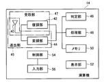
- FIG. 3 is a schematic diagram illustrating an example of a calculator used in the sensing system according to the embodiment of the present invention.
- the computing unit 14 includes an antenna 40, a demodulation unit 42, a modulation unit 44, a determination unit 46, a processing unit 48, a memory 50, a display unit 52, a control unit 54, And an input unit 56.
- the antenna 40 and the modulation unit 44 constitute a transmission unit 45.
- the antenna 40 and the demodulator 42 constitute a receiver 47.
- the antenna 40 is used for receiving various types of information transmitted as radio waves from the sensor tag 12 and transmitting information to the center 16.
- the configuration thereof is not particularly limited as long as the above-described function is performed, and various known antennas can be used.
- the demodulator 42 converts received data received from the sensor tag 12 and the center 16 via the antenna 40 into a form usable by the determination unit 46, the processing unit 48, and the memory 50. For example, the demodulator 42 converts the fine expiration date and correction coefficient value information sent from the center 16 into a form that can be processed by the determination unit 46 and the processor 48 into a form that can be stored in the memory 50. In addition, the demodulator 42 receives the individual recognition information of the sensor tag 12 sent from the sensor tag 12, the measured value measured by the sensor 26, the information on the expiration date of the sensor 26 and the value of the correction coefficient, and the determination unit 46 and the processing unit 48. Is converted into a form that can be stored in the memory 50.
- the demodulation method is not particularly limited, and various known methods can be used.
- the modulation unit 44 converts the individual recognition information of the sensor tag 12 to be written in the memory 28 of the sensor tag 12 into a form that can be received by the sensor tag 12 when transmitted as transmission data.
- the individual recognition information of the sensor tag 12 is transmitted to the center 16 as transmission data, it is converted into a form that can be received by the center 16.
- the modulation method is not particularly limited, and various known methods can be used.
- the determination unit 46 determines whether or not the expiration date of the sensor 26 of the sensor tag 12 received from the center 16 and the expiration date of the sensor 26 stored in the sensor tag 12 are valid at the received date and time.
- the processing unit 48 corrects the measurement value of the sensor 26 using the value of the correction coefficient from the center 16 and obtains the final measurement value of the sensor 26. If the processing unit 48 cannot exchange information with the center 16, the processing unit 48 corrects the measurement value of the sensor 26 using the expiration date of the sensor 26 and the value of the correction coefficient, and obtains the final measurement value of the sensor 26. . In this case, since the value of the correction coefficient from the center 16 is not used, it is possible to avoid a situation in which the measurement value is not obtained but the measurement is impossible because the accuracy is inferior.
- the memory 50 stores the reception data and transmission data described above, measurement values measured by the sensor 26 of the sensor tag 12, individual recognition information of the sensor tag 12, and the like.
- the configuration of the memory 50 is not particularly limited as long as it is a rewritable memory, and various known memories can be used.
- the display unit 52 displays the results obtained by the calculator 14. For example, the measurement value obtained by the sensor 26 is displayed as an image or text. If there are a plurality of objects M, the measurement value obtained by the sensor 26 is displayed for each object M.
- Various types of display devices such as a liquid crystal display panel can be used for the display unit 52.
- the control unit 54 controls each component of the computing machine 14.
- the input unit 56 inputs an instruction to set various setting conditions and the like in the computing machine 14.
- the configuration of the input unit 56 is not particularly limited as long as it performs the above-described function, and a keyboard, a mouse, or the like may be used, and a touch panel may be used.
- the calculator 14 may not include the display unit 52 and the input unit 56.
- the center 16 has a function of receiving the individual recognition information of the sensor tag 12 sent from the computing unit 14, and the expiration date and the value of the correction coefficient stored in the memory 28 of the sensor tag 12 according to the individual recognition information of the sensor tag 12. It has a function of sending the expiration date and the value of the correction coefficient finer than that to the calculator 14.
- FIG. 4 is a schematic diagram illustrating an example of a center used in the sensing system according to the embodiment of the present invention.
- the center 16 includes an antenna 60, a demodulation unit 62, a modulation unit 64, a processing unit 66, a storage unit 68, a display unit 70, a control unit 72, and an input unit 74.
- the antenna 60 and the modulation unit 64 constitute a transmission unit 65.
- the antenna 60 and the demodulator 62 constitute a receiver 67.
- the antenna 60 is used for transmission / reception with the computing unit 14.
- the configuration thereof is not particularly limited as long as the above function is performed, and various known antennas can be used.
- the demodulator 62 converts received data received from the computing unit 14 via the antenna 60 into a form that can be processed by the processor 66.
- the demodulating unit 62 converts the individual recognition information of the sensor tag 12 sent from the computing unit 14 into a form that can be processed by the processing unit 66 and the storage unit 68.
- the demodulation method is not particularly limited, and various known methods can be used.
- the modulation unit 64 converts the information on the fine expiration date and the value of the correction coefficient into a form that can be received by the calculator 14.
- the modulation method is not particularly limited, and various known methods can be used.
- the processing unit 66 reads out information on the fine expiration date and the value of the correction coefficient stored in the storage unit 68 for each individual recognition information, and stores the fine expiration date in the computing unit 14. And information on the value of the correction coefficient. Note that if the center 16 cannot exchange information with the computing device 14 due to equipment failure or the like, the center 16 cannot send detailed information on the expiration date and the value of the correction coefficient to the computing device 14.
- the storage unit 68 stores the individual recognition information from the computing unit 14, the information on the fine expiration date and the value of the correction coefficient for each individual recognition information.
- the configuration of the storage unit 68 is not particularly limited as long as it is a rewritable memory, and various known memories can be used.
- the display unit 70 sends the individual recognition information from the computing unit 14, the information about the computing unit 14 that sent the individual recognition information, the information on the fine expiration date and the value of the correction coefficient for each individual recognition information, and the sending to the computing unit 14. It displays information such as detailed expiration dates and correction coefficient values. If there are a plurality of computing units 14, the above-described various types of information are displayed for each computing unit 14. Various types of display devices such as a liquid crystal display panel can be used for the display unit 70.
- the control unit 72 controls each component of the center 16.
- the input unit 74 can be used to input instructions for setting various setting conditions and the like at the center 16.
- the configuration of the input unit 74 is not particularly limited as long as it performs the above-described function, and a keyboard, a mouse, or the like is used. Note that the display unit 70 and the input unit 74 may not be provided in the center 16.
- the computing unit 14 sends a test signal to the center 16 for establishing communication, and the center 16 sends a reply signal to the test signal. Communication is established when a reply signal is received, and communication is disabled when a reply signal cannot be received.
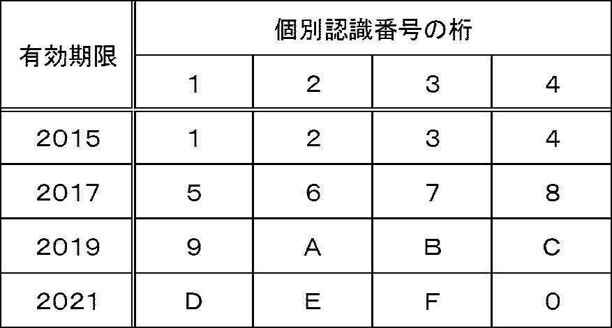
- the expiration date and the correction coefficient stored in the memory 28 of the sensor tag 12 are set in units of years, for example, 2015, 2017, 2019, 2021 for example. Further, the correction coefficient is set as an integer, for example, 1, 2, 3, 4 and there is no setting after the decimal point. In this way, the amount of information stored can be reduced.
- the expiration date and the correction coefficient stored in the storage unit 68 of the center 16 are finer than the expiration date and the correction coefficient stored in the memory 28 of the sensor tag 12. For example, the expiration date is set every other month in the range from 2015 to 2022. For example, the correction coefficient is set in the range of 0.5 to 4.5 every 0.1. In the center 16, it is not necessary to reduce the amount of information to be stored, so that a detailed expiration date and correction coefficient can be set.
- the expiration date and the correction coefficient stored in the storage unit 68 of the center 16 are finer than the expiration date and the correction coefficient stored in the memory 28 of the sensor tag 12.
- the expiration date and the correction coefficient stored in the memory 28 of the sensor tag 12 are relatively coarse as compared to the center 16 due to information amount restrictions and the like.
- the number of bits in binary number is at least one digit smaller. For example, if the coarse one is 2 bits, the fine one is 3 bits.
- the number of bits in binary numbers is preferably at least 8 digits smaller, and for fine ones, the number of bits in binary numbers is more preferably at least 10 digits or less. .
- An individual identification number is assigned to the sensor tag 12 as individual identification information, which is given using, for example, Table 1 below.
- the correction coefficient of the sensor 26 is measured to obtain, for example, an expiration date 2017.10 and a correction coefficient 0.6.
- This combination of numerical values is a combination of a fine expiration date and a correction coefficient stored in the center 16.
- the first digit of the individual identification number is given using Table 1 below. From Table 1 below, the number of the first digit is 5 when the expiration date is 2017.
- the sensor tag 12 with the first digit of 5 is given a 4-digit number with 5001 from the first, and the second sensor tag 12 is 5002.
- the expiration date is 2017. If the use date / time of the sensor tag 12 is 2017.1.1 or earlier as in 2016.10, the correction coefficient set with the rough expiration date 2017 is used. At this time, since the correction coefficient is coarse, for example, if the temperature is measured, the measurement results of the temperature are 37 ° C. and 38 ° C., and the precision after the decimal point cannot be obtained. As the temperature, 37 ° C. and 38 ° C. are displayed. On the other hand, when the computing unit 14 can transmit and receive with the center 16, the expiration date 2017.10 and the correction coefficient 0.6 can be obtained based on the individual identification number.
- the numerical values of the temperatures obtained can be, for example, 37.5 ° C. and 38.5 ° C., and the precision after the decimal point can be obtained.
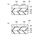
- FIG. 5A is a schematic cross-sectional view showing a first example of a configuration of a thin film transistor including a coated semiconductor used in the sensor tag according to the embodiment of the present invention in a semiconductor active layer
- FIG. It is a typical cross section which shows the 2nd example of a structure of the thin-film transistor which contains the coating type semiconductor used for the sensor tag of embodiment in a semiconductor active layer.
- the coating type TFT includes the coating type semiconductor in the semiconductor active layer, but may further include other layers in addition to the semiconductor active layer.
- the coating type TFT is preferably an organic field effect transistor (hereinafter simply referred to as FET), and more preferably an insulated gate FET in which the gate and the channel are insulated.
- FET organic field effect transistor
- the structure of the coating type TFT is not particularly limited, and various known structures can be employed.
- a structure bottom gate / top contact type in which an electrode, an insulator layer, a semiconductor active layer (organic semiconductor layer), and two electrodes are sequentially arranged on the upper surface of the lowermost substrate.
- the electrode on the upper surface of the lowermost substrate is provided on a part of the substrate, and the insulator layer is disposed so as to be in contact with the substrate at a portion other than the electrode.
- the two electrodes provided on the upper surface of the semiconductor active layer are arranged separately from each other.
- an insulating substrate 82 is disposed in the lowermost layer, a gate electrode 84 is provided on a part of the upper surface of the substrate 82, and the gate electrode 84 is covered and other than the gate electrode 84.
- An insulating layer 86 is provided so as to be in contact with the substrate 82 at the portion.
- a semiconductor active layer 88 is provided on the upper surface of the insulator layer 86, and the source electrode 90a and the drain electrode 90b are disposed separately on a part of the upper surface of the semiconductor active layer 88.
- bottom gate / bottom contact type elements As coating type TFTs, there are bottom gate / bottom contact type elements as coating type TFTs.
- the configuration of the bottom gate / bottom contact type element is shown in FIG.
- the same components as those in the coating TFT 80 shown in FIG. 5A are denoted by the same reference numerals, and detailed description thereof is omitted.
- an insulating substrate 82 is disposed in the lowermost layer, a gate electrode is provided on a part of the upper surface of the substrate 82, the gate electrode 84 is covered, and the substrate 82 is in contact with a portion other than the gate electrode 84.
- An insulator layer 86 is provided. Further, the source electrode 90a and the drain electrode 90b are disposed separately on a part of the upper surface of the insulator layer 86.
- a semiconductor active layer 88 is provided so as to cover the source electrode 90a and the drain electrode 90b and to be in contact with the insulator layer 86 at a portion other than the source electrode 90a and the drain electrode 90b. Below the layer 88.
- the coating type TFT 80a shown in FIG. 5B is an insulated gate type in which a channel serving as a current path between the drain and the source and the gate electrode 84 are insulated. FET.
- an insulator, a top gate / top contact type element having a gate electrode above the semiconductor active layer, or a top gate / bottom contact type element can also be preferably used.
- the thickness of the whole transistor is preferably set to 0.1 to 0.5 ⁇ m.
- the coating type TFT 80, 80a is entirely sealed with a metal sealing can in order to shield the coating type TFT 80, 80a from the air and moisture and to improve the storage stability of the coating type TFT 80, 80a, glass, silicon nitride, etc.
- These may be sealed with an inorganic material, a polymer material such as parylene, or a low molecular material.
- the substrate material is not particularly limited as long as it has insulating properties, and a known material can be used.
- polyester films such as polyethylene naphthalate (PEN) and polyethylene terephthalate (PET), cycloolefin polymer film, polycarbonate film, triacetyl cellulose (TAC) film, or polyimide film, and these polymer films are bonded to ultrathin glass.
- PEN polyethylene naphthalate
- PET polyethylene terephthalate
- TAC triacetyl cellulose
- polyimide film polyimide film
- a metal material such as Cr, Al, Ta, Mo, Nb, Cu, Ag, Au, Pt, Pd, In, Ni, or Nd, or an alloy thereof Material can be used.
- a known conductive material such as a carbon material or a conductive polymer can be used as a constituent material of the electrode, and any conductive material can be used without particular limitation.
- the thicknesses of the gate electrode, source electrode, and drain electrode are not particularly limited, but are preferably 10 to 50 nm.
- the coating type TFT preferably includes an acceptor for promoting carrier injection.
- Preferred examples of the material include known 2,3,5,6-tetrafluoro-7,7,8,8-tetracyanoquinodimethane (F4-TCNQ).
- F4-TCNQ 2,3,5,6-tetrafluoro-7,7,8,8-tetracyanoquinodimethane
- the thickness of the acceptor is not particularly limited, but is preferably 5 nm or less.
- the material constituting the insulating layer is not particularly limited as long as a necessary insulating effect can be obtained.
- fluoropolymer insulating materials such as silicon dioxide, silicon nitride, PTFE (polytetrafluoroethylene), CYTOP (registered trademark)
- polyester insulating materials polycarbonate insulating materials, acrylic polymer insulating materials, epoxy resin insulating materials, polyimide insulating materials, polyvinyl phenol resin insulating materials, and polyparaxylene resin insulating materials.
- the upper surface of the insulating layer may be subjected to surface treatment, for example, an insulating material in which the surface of silicon dioxide is surface-treated by application of hexamethyldisilazane (HMDS), octadecyltrichlorosilane (OTS), or ⁇ -phenethyltrimethoxysilane.
- HMDS hexamethyldisilazane
- OTS octadecyltrichlorosilane
- ⁇ -phenethyltrimethoxysilane ⁇ -phenethyltrimethoxysilane.
- the thickness of the insulating layer is not particularly limited, but when thinning is required, the thickness is preferably 10 to 500 nm, more preferably 20 to 200 nm, and particularly preferably 50 to 200 nm. .
- examples of the compound contained in the semiconductor active layer that can be formed by the coating method include the following organic semiconductor compounds.
- organic semiconductor compounds include polycyclic aromatic hydrocarbons such as pentacene, anthracene and rubrene, low molecular compounds such as tetracyanoxydimethane, and polyacetylene, polypyrrole, polyaniline, poly-3-hexylthiophene, polyparaphenylene vinylene, etc.
- the polymer may further contain a polymer binder in addition to the organic semiconductor compound described above. Moreover, the residual solvent at the time of formation of a semiconductor active layer may be contained.
- the content of the polymer binder in the semiconductor active layer is not particularly limited, but is preferably used in the range of 0 to 95% by mass, more preferably in the range of 10 to 90% by mass, and still more preferably. It is used in the range of 20 to 80% by mass, particularly preferably in the range of 30 to 70% by mass.
- the thickness of the semiconductor active layer is not particularly limited, but when thinning is required, the thickness is preferably 10 to 400 nm, more preferably 10 to 200 nm, and particularly preferably 10 to 100 nm. preferable.
- the semiconductor active layer can be formed by a coating method.
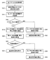
- FIG. 6 is a flowchart showing an example of temperature measurement in the sensing system according to the embodiment of the present invention.
- the sensor tag 12 is attached to the object M.
- a description will be given by taking as an example temperature measurement of the food when the object M is used as a food and the food is stored in a refrigerator.
- the sensor tag 12 has a temperature sensor as the sensor 26.
- a correction coefficient and an expiration date for the temperature sensor are obtained in advance, and the expiration date and the correction coefficient for the temperature sensor are stored in the memory 28.
- the memory 28 of the sensor tag 12 stores an individual recognition number as individual recognition information.
- the sensor tag 12 is attached to the food material that is the object M, and stored in the refrigerator.
- the sensor tag 12 is assigned an individual identification number, and the expiration date and correction coefficient of the sensor 26 are stored. Further, a fine expiration date and a correction coefficient are stored in the center 16.
- step S10 the temperature is measured by the sensor 26 (step S10). Then, a temperature measurement value is obtained by the sensor 26. An individual recognition number and a temperature measurement value of the sensor 26 are transmitted from the sensor tag 12 to the computing unit 14 as individual recognition information (step S12). The calculator 14 transmits the received information of the individual identification number to the center 16 (step S14). Next, communication with the center 16 is confirmed (step S16). In this case, it is assumed that the computing unit 14 sends a test signal to the center 16 for establishing communication, and communication is established when there is a reply signal from the center 16 to the test signal. On the other hand, when the reply signal cannot be received, that is, when the calculator 14 cannot exchange information with the center 16, communication is disabled.
- the center 16 transmits an expiration date and a correction coefficient smaller than those stored in the sensor tag 12 to the calculator 14 according to the individual identification number (Ste S18).
- the calculator 14 receives the fine expiration date and the correction coefficient (step S20).
- the expiration date is determined by the calculator 14 (step S22). If it is within the expiration date, it is corrected using the correction coefficient, and a final temperature measurement value is calculated (step S24).
- the computing unit 14 transmits the expiration date and correction coefficient of the sensor 26 to the sensor tag 12 for reception (step S26).
- the measured temperature value has a lower correction accuracy and a smaller number of significant digits than those using a fine expiration date and a correction coefficient.
- the measured temperature value is displayed on, for example, the display unit 52 of the calculator 14 or the display unit 70 of the center 16.
- step S16 when communication with the center 16 is impossible, the computing unit 14 transmits the expiration date and correction coefficient of the sensor 26 to the sensor tag 12 for reception (step S30). And it correct
- the measured temperature value has a lower correction accuracy and a smaller number of significant digits than those using a fine expiration date and a correction coefficient.
- the measured temperature value is displayed on, for example, the display unit 52 of the calculator 14 or the display unit 70 of the center 16.
- the sensing system 10 can know the temperature of the ingredients in the refrigerator. If the temperature is measured at an equal time interval such as one hour interval, the temperature change of the food in the refrigerator can be known. Further, when the object M is an animal or a human, changes in body temperature can be known. Other physical quantities or chemical quantities can be measured by using other sensors instead of temperature sensors. Moreover, although the expiration date and correction coefficient of the sensor 26 are stored in the sensor tag 12, the amount of information is reduced and the memory capacity of the sensor tag 12 is not increased. For this reason, even if the expiration date and the correction coefficient of the sensor 26 are stored, the configuration of the sensor tag 12 is not complicated. The center 16 stores a detailed expiration date and a correction coefficient. By using the correction coefficient of the center 16, the measured value can be calculated with higher accuracy.
- the present invention is basically configured as described above.
- the sensing system of the present invention has been described in detail above.
- the present invention is not limited to the above-described embodiment, and various modifications or changes may be made without departing from the spirit of the present invention. .
Landscapes
- Physics & Mathematics (AREA)
- General Physics & Mathematics (AREA)
- Engineering & Computer Science (AREA)
- Computer Networks & Wireless Communication (AREA)
- Arrangements For Transmission Of Measured Signals (AREA)
- Indication And Recording Devices For Special Purposes And Tariff Metering Devices (AREA)
- Testing Or Calibration Of Command Recording Devices (AREA)
Abstract
This sensing system has: a sensor tag provided with a sensor for measuring a physical quantity, chemical quantity, or the like, memory for storing period of validity and correction coefficient values for the sensor and individual identification information, and a transmission unit for transmitting the measured values and the individual identification information of the sensor to a computation unit; a center provided with a storage unit for storing detailed period of validity and correction coefficient values for each item of individual identification information and a transmission unit for transmitting the detailed period of validity and correction coefficient values corresponding to individual identification information to the computation unit; and the computation unit, which is provided with a transmission unit for transmitting individual identification information to the center, a reception unit for receiving individual identification information, measured values, and detailed period of validity and correction coefficient values, a determination unit for determining a period of validity, and a processing unit for using the correction coefficient values to correct the measured values.
Description
本発明は、物理量および化学量のうち、少なくとも1つを測定するセンサを無線タグ、ICタグ(電子タグ)またはRFID(radio frequency identifier)等に組み込んだセンサタグを用いたセンシングシステムに関し、特に、センサを組み込んでも構成が複雑になることがなく、かつセンサタグが、補正値等が記憶された外部との情報のやり取りができない状況であっても、センサによる測定が可能なセンシングシステムに関する。
The present invention relates to a sensing system using a sensor tag in which a sensor for measuring at least one of a physical quantity and a chemical quantity is incorporated in a wireless tag, an IC tag (electronic tag), an RFID (radio frequency identifier), or the like. The present invention relates to a sensing system that can be measured by a sensor even when the sensor tag is not complicated and the sensor tag cannot exchange information with the outside in which correction values and the like are stored.
現在、無線タグ、ICタグまたはRFID等と呼ばれるものは、小型であり、かつ識別情報を非接触で読み取ることができるため種々の用途に用いられている。例えば、ガスセンサ、超音波センサ、湿度センサ、水分センサ、温度センサ、光センサ、放射線センサ、磁気センサ、圧力センサ、pHセンサ、濁度センサ、高度センサ、加速度センサ等のセンサを、無線タグ、ICタグまたはRFID等に組み込むことで、種々の物理量または化学量を測定することが試みられている。
Currently, what are called wireless tags, IC tags, RFIDs, and the like are used for various purposes because they are small and can read identification information in a non-contact manner. For example, sensors such as gas sensors, ultrasonic sensors, humidity sensors, moisture sensors, temperature sensors, light sensors, radiation sensors, magnetic sensors, pressure sensors, pH sensors, turbidity sensors, altitude sensors, acceleration sensors, wireless tags, ICs Attempts have been made to measure various physical quantities or chemical quantities by incorporating them into tags or RFIDs.
しかし、センサを構成する回路にはばらつきがあり、センサで測定される測定値の絶対値が変化するので、通常、補正値の記録、または補正回路の組み込みが必要であり、構成が複雑になる。このため、無線タグ、ICタグまたはRFID等にセンサを組み込んだ場合でも簡便な構成のものが求められている。
However, since the circuits constituting the sensor vary and the absolute value of the measured value measured by the sensor changes, it is usually necessary to record a correction value or incorporate a correction circuit, which complicates the configuration. . For this reason, even when a sensor is incorporated in a wireless tag, IC tag, RFID, or the like, a simple configuration is required.
例えば、特許文献1には、センサ本体と、識別情報を記憶させたメモリと、少なくともセンサ本体の検出データを送出する送信部とを一体化したセンサチップと、センサチップから送出された検出データを受信する受信部と、受信部から出力される検出データをセンサ本体の種別に応じて補正する信号補正部とを備えた信号処理部とを含むセンサシステムが記載されている。信号補正部は、センサ本体に対応した基準データを有し、センサチップから出力される検出データと基準データとを比較して検出データを補正する。特許文献1では、信号補正部で検出データをセンサ本体の種別に応じて補正しており、センサチップにセンサ本体の補正手段を組み込む必要がない。
For example, Patent Document 1 discloses a sensor chip in which a sensor main body, a memory storing identification information, and a transmission unit that transmits at least detection data of the sensor main body are integrated, and detection data sent from the sensor chip. A sensor system is described that includes a receiving unit that receives a signal and a signal processing unit that corrects detection data output from the receiving unit according to the type of the sensor body. The signal correction unit has reference data corresponding to the sensor body, and corrects the detection data by comparing the detection data output from the sensor chip with the reference data. In Patent Document 1, the signal correction unit corrects the detection data according to the type of the sensor body, and there is no need to incorporate the sensor body correction means into the sensor chip.
しかしながら、特許文献1のように、検出データをセンサ本体の種別に応じて補正する信号補正部をセンサチップの外部に設けた場合、センサチップと信号処理部との間での情報のやり取りができない場合、例えば、通信不能になると、センサの測定ができなくなるという問題点がある。このため、センサチップと信号処理部とが通信不能でもセンサによる測定ができることが求められている。
However, as in Patent Document 1, when a signal correction unit that corrects detection data according to the type of the sensor body is provided outside the sensor chip, information cannot be exchanged between the sensor chip and the signal processing unit. In this case, for example, when communication is disabled, there is a problem that the sensor cannot be measured. For this reason, even if a sensor chip and a signal processing part cannot communicate, it is calculated | required that a sensor can measure.
本発明の目的は、前述の従来技術に基づく問題点を解消し、センサを組み込んでも構成が複雑になることがなく、かつセンサタグが、補正値等が記憶された外部との情報のやり取りができない状況であっても、センサによる測定が可能なセンシングシステムを提供することにある。
The object of the present invention is to solve the above-mentioned problems based on the prior art, the structure is not complicated even if a sensor is incorporated, and the sensor tag cannot exchange information with the outside in which correction values are stored. It is to provide a sensing system capable of measurement by a sensor even in a situation.
上記目的を達成するために、本発明は、センサタグと演算機とセンタとを有するセンシングシステムであって、センサタグは、物理量および化学量のうち、少なくとも1つを測定するセンサと、センサの有効期限および補正係数の値、ならびに個別認識情報を記憶するメモリと、センサで測定された測定値と個別認識情報、ならびにセンサの有効期限および補正係数の値を演算機に送出する送出部とを有し、センタは、個別認識情報ごとにセンサタグのメモリに記憶された有効期限および補正係数の値よりも細かい有効期限および補正係数の値が記憶された記憶部と、演算機に個別認識情報に応じた細かい有効期限および補正係数の値を送出する送出部とを有し、演算機は、センサタグの個別認識情報をセンタに送出する送出部と、センサタグの送出部から個別認識情報と測定値、センタから細かい有効期限および補正係数の値を受け取る受取部と、センタからの細かい有効期限を判定する判定部と、センタからの補正係数の値を用いて測定値を補正する処理部とを有し、演算機は、センタと情報のやり取りができない場合、処理部でセンサの有効期限および補正係数の値を用いて測定値を補正することを特徴とするセンシングシステムを提供するものである。
In order to achieve the above object, the present invention is a sensing system having a sensor tag, a computing unit, and a center, wherein the sensor tag includes a sensor for measuring at least one of a physical quantity and a chemical quantity, and an expiration date of the sensor. And a memory for storing correction coefficient values and individual recognition information, and a sending unit for sending measured values measured by the sensor and individual recognition information, as well as sensor expiry date and correction coefficient values to a calculator. The center has a storage unit that stores an expiration date and correction coefficient values that are smaller than the expiration date and correction coefficient values stored in the sensor tag memory for each individual recognition information, and a computing unit that responds to the individual recognition information. A computing unit that sends out the individual recognition information of the sensor tag to the center, and a sensor. A receiving unit that receives individual recognition information and measured values from the sending unit, a fine expiration date and a correction coefficient value from the center, a determination unit that determines a fine expiration date from the center, and a correction coefficient value from the center A processing unit that corrects the measured value, and when the calculator cannot exchange information with the center, the processing unit corrects the measured value using the expiration date of the sensor and the value of the correction coefficient. A sensing system is provided.
センサタグは、塗布型半導体を半導体活性層に含む薄膜トランジスタを有することが好ましい。また、センサタグは、センサの補正係数が測定された後、メモリに個別認識情報が不揮発的に書き込まれることが好ましい。
センサタグのメモリは、情報を1度だけ書き込むことができるものであることが好ましい。 The sensor tag preferably includes a thin film transistor including a coating type semiconductor in a semiconductor active layer. Moreover, it is preferable that the sensor tag has the individual recognition information written in the memory in a nonvolatile manner after the correction coefficient of the sensor is measured.
The memory of the sensor tag is preferably capable of writing information only once.
本発明のセンシングシステムによれば、センサを組み込んでも構成が複雑になることがなく、かつ演算機が、補正値等が記憶されたセンタとの情報のやり取りができない状況であっても、センサによる測定が可能である。
According to the sensing system of the present invention, even if a sensor is incorporated, the configuration does not become complicated, and even if the arithmetic unit cannot exchange information with the center in which correction values are stored, Measurement is possible.
以下に、添付の図面に示す好適実施形態に基づいて、本発明のセンシングシステムを詳細に説明する。
図1は、本発明の実施形態のセンシングシステムの構成を示す模式図である。図2は、本発明の実施形態のセンシングシステムに用いられるセンサタグの一例を示す模式図である。 Hereinafter, a sensing system of the present invention will be described in detail based on a preferred embodiment shown in the accompanying drawings.
FIG. 1 is a schematic diagram illustrating a configuration of a sensing system according to an embodiment of the present invention. FIG. 2 is a schematic diagram illustrating an example of a sensor tag used in the sensing system according to the embodiment of the present invention.
図1に示すセンシングシステム10は、対象物Mに取り付けられたセンサタグ12と、演算機14と、センタ16とを有する。
センシングシステム10は、無線タグ、ICタグ(電子タグ)またはRFID(radio frequency identifier)等にセンサを組み込んだセンサタグ12を用いて、種々の物理量または化学量を測定することができる。
なお、対象物Mとは、測定対象物のことである。測定対象物とは、体温、被服の温度等を測定する場合には動物および人間等であり、冷蔵保存、冷凍保存の温度を測定する場合には、肉、魚、野菜等の食材である。また、固体または液体の温度を測定する場合には、固体または液体が対象物Mとなる。 Asensing system 10 illustrated in FIG. 1 includes a sensor tag 12 attached to an object M, a calculator 14, and a center 16.
Thesensing system 10 can measure various physical quantities or chemical quantities using a sensor tag 12 in which a sensor is incorporated in a wireless tag, an IC tag (electronic tag), an RFID (radio frequency identifier), or the like.
The object M is a measurement object. Measurement objects include animals and humans when measuring body temperature, clothing temperature, and the like, and foods such as meat, fish, and vegetables when measuring refrigerated storage and frozen storage temperatures. Further, when measuring the temperature of the solid or liquid, the solid or liquid becomes the object M.
センシングシステム10は、無線タグ、ICタグ(電子タグ)またはRFID(radio frequency identifier)等にセンサを組み込んだセンサタグ12を用いて、種々の物理量または化学量を測定することができる。
なお、対象物Mとは、測定対象物のことである。測定対象物とは、体温、被服の温度等を測定する場合には動物および人間等であり、冷蔵保存、冷凍保存の温度を測定する場合には、肉、魚、野菜等の食材である。また、固体または液体の温度を測定する場合には、固体または液体が対象物Mとなる。 A
The
The object M is a measurement object. Measurement objects include animals and humans when measuring body temperature, clothing temperature, and the like, and foods such as meat, fish, and vegetables when measuring refrigerated storage and frozen storage temperatures. Further, when measuring the temperature of the solid or liquid, the solid or liquid becomes the object M.
センサタグ12は、物理量および化学量のうち、少なくとも1つを測定する機能を有し、個別認識情報、いわゆる個別認識番号(ID)が記憶されており、センサタグ12の個別認識情報、センサ26で測定して得られた測定値、ならびにセンサ26の有効期限および補正係数を外部に送出する機能を有する。センサタグ12は、例えば、アクティブタイプと呼ばれるものが用いられる。
The sensor tag 12 has a function of measuring at least one of a physical quantity and a chemical quantity, and stores individual recognition information, so-called individual identification number (ID), and is measured by the individual recognition information of the sensor tag 12 and the sensor 26. The measured value obtained in this way, and the expiration date and correction coefficient of the sensor 26 are transmitted to the outside. As the sensor tag 12, for example, a so-called active type is used.
具体的には、図2に示すセンサタグ12は、絶縁性の基板20の周縁部に沿って形成されたアンテナ22と、このアンテナ22に接続されて、基板20に設けられたICチップ24と、センサ26と、メモリ28と、電源部30とを有する。ICチップ24は、アンテナ22とともに、センサタグ12内の各種の情報を演算機14に送出する送出部25を構成する。送出部25により、ICチップ24によりアンテナ22を介してセンサタグ12内の各種の情報が電波として演算機14に送出される。図2に示すセンサタグ12ではアンテナ22を用いた無線形式で送出部25を構成したが、これに限定されるものではなく、送出部25は有線形式でもよい。
なお、送出部25は、後述するようにセンサタグ12に送信された情報を受け取る受信部としても機能するものである。 Specifically, thesensor tag 12 shown in FIG. 2 includes an antenna 22 formed along the peripheral edge of the insulating substrate 20, an IC chip 24 provided on the substrate 20 connected to the antenna 22, A sensor 26, a memory 28, and a power supply unit 30 are included. The IC chip 24, together with the antenna 22, constitutes a sending unit 25 that sends various types of information in the sensor tag 12 to the computing unit 14. Various kinds of information in the sensor tag 12 are sent out as radio waves to the computing unit 14 by the sending unit 25 through the antenna 22 by the IC chip 24. In the sensor tag 12 shown in FIG. 2, the transmission unit 25 is configured in a wireless format using the antenna 22, but the present invention is not limited to this, and the transmission unit 25 may be in a wired format.
The sendingunit 25 also functions as a receiving unit that receives information transmitted to the sensor tag 12 as will be described later.
なお、送出部25は、後述するようにセンサタグ12に送信された情報を受け取る受信部としても機能するものである。 Specifically, the
The sending
ICチップ24は、パッケージされた半導体集積回路であり、変調回路(図示せず)と、復調回路(図示せず)とRF回路(図示せず)を備える。変調回路により、センサタグ12の個別認識情報、センサ26の測定値、ならびにセンサ26の有効期限および補正係数を送信データとしてアンテナ22を介して演算機14に送信する際に、演算機14で受け取り可能な形態に変換するものである。変調方式としては、特に限定されるものではなく、公知のものを種々用いることができる。
The IC chip 24 is a packaged semiconductor integrated circuit, and includes a modulation circuit (not shown), a demodulation circuit (not shown), and an RF circuit (not shown). When the modulation circuit transmits the individual recognition information of the sensor tag 12, the measured value of the sensor 26, and the expiration date and correction coefficient of the sensor 26 as transmission data to the calculator 14 via the antenna 22, it can be received by the calculator 14. It is converted into a different form. The modulation method is not particularly limited, and various known methods can be used.
復調回路により、演算機14からアンテナ22を介して受信した受信データを、メモリ28で利用可能な形態に変換するものである。復調方式としては、特に限定されるものではなく、公知のものを種々用いることができる。
また、RF回路は、アンテナ22を介して内部の各種の情報を演算機14に送出するためのものである。RF回路は、ICタグ、RFID等で用いられている公知のものを適宜利用可能である。 The demodulating circuit converts the received data received from thecomputing unit 14 via the antenna 22 into a form usable by the memory 28. The demodulation method is not particularly limited, and various known methods can be used.
The RF circuit is for sending various internal information to thecomputing unit 14 via the antenna 22. As the RF circuit, a known circuit used in an IC tag, RFID, or the like can be used as appropriate.
また、RF回路は、アンテナ22を介して内部の各種の情報を演算機14に送出するためのものである。RF回路は、ICタグ、RFID等で用いられている公知のものを適宜利用可能である。 The demodulating circuit converts the received data received from the
The RF circuit is for sending various internal information to the
センサ26は、物理量および化学量のうち、少なくとも1つを測定するものである。センサ26は特に限定されるものではなく、例えば、ガスセンサ、超音波センサ、湿度センサ、水分センサ、温度センサ、光センサ、放射線センサ、磁気センサ、圧力センサ、pHセンサ、濁度センサ、高度センサ、加速度センサ等を用いることができる。センサ26の数は1つに限定されるものではなく、上述の各種のセンサを複数組み合わせたものでもよい。
The sensor 26 measures at least one of physical quantity and chemical quantity. The sensor 26 is not particularly limited. For example, a gas sensor, an ultrasonic sensor, a humidity sensor, a moisture sensor, a temperature sensor, a light sensor, a radiation sensor, a magnetic sensor, a pressure sensor, a pH sensor, a turbidity sensor, an altitude sensor, An acceleration sensor or the like can be used. The number of sensors 26 is not limited to one, and may be a combination of a plurality of the various sensors described above.
メモリ28は、センサ26の有効期限および補正係数の値、センサ26で測定して得られた測定値、ならびにセンサタグ12の個別認識情報を記憶するものである。このメモリ28は、例えば、不揮発性メモリで構成される。また、メモリ28は、情報を1度だけ書き込むことができるもの、ライトワンスのものであってもよい。
電源部30は、ICチップ24の変調回路、復調回路、RF回路(高周波回路)を駆動するものであり、またセンサ26の測定にも利用される。 Thememory 28 stores the expiration date of the sensor 26 and the value of the correction coefficient, the measurement value obtained by measurement with the sensor 26, and the individual recognition information of the sensor tag 12. The memory 28 is composed of, for example, a nonvolatile memory. Further, the memory 28 may be one that can write information only once or one that is write-once.
The power supply unit 30 drives a modulation circuit, a demodulation circuit, and an RF circuit (high frequency circuit) of theIC chip 24 and is also used for measurement of the sensor 26.
電源部30は、ICチップ24の変調回路、復調回路、RF回路(高周波回路)を駆動するものであり、またセンサ26の測定にも利用される。 The
The power supply unit 30 drives a modulation circuit, a demodulation circuit, and an RF circuit (high frequency circuit) of the
ICチップ24およびメモリ28は、複数のトランジスタで構成されるが、このトランジスタは、塗布型半導体を半導体活性層に含む薄膜トランジスタ(以下、単に塗布型TFTという)で構成することが好ましい。塗布型TFTは、作製に要する温度が低いこと印刷で形成可能といった利点があるため、樹脂基板を用いたセンサタグを安価に実現できる。
しかし、塗布型TFTは記録容量が小さく、記憶する情報量を小さくする必要がある。このため、メモリ28に記憶されるセンサ26の有効期限および補正係数の値およびセンサタグ12の個別認識情報、ならびにセンサ26で測定して得られた測定値は、少ないビット数で記憶することが好ましい。なお、塗布型TFTについては後に詳細に説明する。 TheIC chip 24 and the memory 28 are constituted by a plurality of transistors, and these transistors are preferably constituted by thin film transistors (hereinafter simply referred to as coating type TFTs) including a coating type semiconductor in a semiconductor active layer. The coating type TFT has an advantage that the temperature required for production is low and can be formed by printing. Therefore, a sensor tag using a resin substrate can be realized at low cost.
However, the coating type TFT has a small recording capacity, and it is necessary to reduce the amount of information to be stored. For this reason, it is preferable that the expiration date of the sensor 26 and the value of the correction coefficient, the individual recognition information of thesensor tag 12, and the measurement value obtained by measurement with the sensor 26 are stored in a small number of bits. . The coating type TFT will be described in detail later.
しかし、塗布型TFTは記録容量が小さく、記憶する情報量を小さくする必要がある。このため、メモリ28に記憶されるセンサ26の有効期限および補正係数の値およびセンサタグ12の個別認識情報、ならびにセンサ26で測定して得られた測定値は、少ないビット数で記憶することが好ましい。なお、塗布型TFTについては後に詳細に説明する。 The
However, the coating type TFT has a small recording capacity, and it is necessary to reduce the amount of information to be stored. For this reason, it is preferable that the expiration date of the sensor 26 and the value of the correction coefficient, the individual recognition information of the
以下、演算機14について詳細に説明する。
図3は、本発明の実施形態のセンシングシステムに用いられる演算機の一例を示す模式図である。
演算機14は、図3に示すように、アンテナ40と、復調部42と、変調部44と、判定部46と、処理部48と、メモリ50と、表示部52と、制御部54と、入力部56とを有する。アンテナ40と変調部44とで送出部45が構成される。アンテナ40と復調部42とで受取部47が構成される。 Hereinafter, thecalculator 14 will be described in detail.
FIG. 3 is a schematic diagram illustrating an example of a calculator used in the sensing system according to the embodiment of the present invention.
As shown in FIG. 3, thecomputing unit 14 includes an antenna 40, a demodulation unit 42, a modulation unit 44, a determination unit 46, a processing unit 48, a memory 50, a display unit 52, a control unit 54, And an input unit 56. The antenna 40 and the modulation unit 44 constitute a transmission unit 45. The antenna 40 and the demodulator 42 constitute a receiver 47.
図3は、本発明の実施形態のセンシングシステムに用いられる演算機の一例を示す模式図である。
演算機14は、図3に示すように、アンテナ40と、復調部42と、変調部44と、判定部46と、処理部48と、メモリ50と、表示部52と、制御部54と、入力部56とを有する。アンテナ40と変調部44とで送出部45が構成される。アンテナ40と復調部42とで受取部47が構成される。 Hereinafter, the
FIG. 3 is a schematic diagram illustrating an example of a calculator used in the sensing system according to the embodiment of the present invention.
As shown in FIG. 3, the
アンテナ40は、センサタグ12から電波として送出される各種の情報の受信、およびセンタ16への情報の送信に利用されるものである。アンテナ40としては、上述の機能を果たせば、その構成は、特に限定されるものではなく、公知のものを種々用いることができる。
The antenna 40 is used for receiving various types of information transmitted as radio waves from the sensor tag 12 and transmitting information to the center 16. As the antenna 40, the configuration thereof is not particularly limited as long as the above-described function is performed, and various known antennas can be used.
復調部42は、センサタグ12およびセンタ16からアンテナ40を介して受信した受信データを、判定部46、処理部48、メモリ50で利用可能な形態に変換するものである。例えば、復調部42では、センタ16から送出される細かい有効期限および補正係数の値の情報を、判定部46および処理部48で処理可能な形態に、メモリ50に記憶可能な形態に変換する。
また、復調部42は、センサタグ12から送出されるセンサタグ12の個別認識情報、センサ26で測定された測定値、センサ26の有効期限および補正係数の値の情報を、判定部46および処理部48で処理可能な形態に、メモリ50に記憶可能な形態に変換する。なお、復調方式としては、特に限定されるものではなく、公知のものを種々用いることができる。 Thedemodulator 42 converts received data received from the sensor tag 12 and the center 16 via the antenna 40 into a form usable by the determination unit 46, the processing unit 48, and the memory 50. For example, the demodulator 42 converts the fine expiration date and correction coefficient value information sent from the center 16 into a form that can be processed by the determination unit 46 and the processor 48 into a form that can be stored in the memory 50.
In addition, thedemodulator 42 receives the individual recognition information of the sensor tag 12 sent from the sensor tag 12, the measured value measured by the sensor 26, the information on the expiration date of the sensor 26 and the value of the correction coefficient, and the determination unit 46 and the processing unit 48. Is converted into a form that can be stored in the memory 50. The demodulation method is not particularly limited, and various known methods can be used.
また、復調部42は、センサタグ12から送出されるセンサタグ12の個別認識情報、センサ26で測定された測定値、センサ26の有効期限および補正係数の値の情報を、判定部46および処理部48で処理可能な形態に、メモリ50に記憶可能な形態に変換する。なお、復調方式としては、特に限定されるものではなく、公知のものを種々用いることができる。 The
In addition, the
変調部44は、センサタグ12のメモリ28に書き込むセンサタグ12の個別認識情報を送信データとして送信する際にセンサタグ12で受け取り可能な形態に変換するものである。また、センタ16にセンサタグ12の個別認識情報を送信データとして送信する際に、センタ16で受け取り可能な形態に変換するものである。変調方式としては、特に限定されるものではなく、公知のものを種々用いることができる。
The modulation unit 44 converts the individual recognition information of the sensor tag 12 to be written in the memory 28 of the sensor tag 12 into a form that can be received by the sensor tag 12 when transmitted as transmission data. In addition, when the individual recognition information of the sensor tag 12 is transmitted to the center 16 as transmission data, it is converted into a form that can be received by the center 16. The modulation method is not particularly limited, and various known methods can be used.
判定部46は、センタ16から受信したセンサタグ12のセンサ26の有効期限およびセンサタグ12に記憶されたセンサ26の有効期限が、受信した日時において有効であるか否かを判定するものである。
処理部48は、センタ16からの補正係数の値を用いてセンサ26の測定値を補正し、最終的なセンサ26での測定値を得るものである。また、処理部48は、センタ16と情報をやり取りができない場合、センサ26の有効期限および補正係数の値を用いてセンサ26の測定値を補正し、最終的なセンサ26での測定値を得る。この場合、センタ16からの補正係数の値を用いていないため、精度は劣るが測定値が得られず、測定不能になるという事態を回避することができる。 Thedetermination unit 46 determines whether or not the expiration date of the sensor 26 of the sensor tag 12 received from the center 16 and the expiration date of the sensor 26 stored in the sensor tag 12 are valid at the received date and time.
Theprocessing unit 48 corrects the measurement value of the sensor 26 using the value of the correction coefficient from the center 16 and obtains the final measurement value of the sensor 26. If the processing unit 48 cannot exchange information with the center 16, the processing unit 48 corrects the measurement value of the sensor 26 using the expiration date of the sensor 26 and the value of the correction coefficient, and obtains the final measurement value of the sensor 26. . In this case, since the value of the correction coefficient from the center 16 is not used, it is possible to avoid a situation in which the measurement value is not obtained but the measurement is impossible because the accuracy is inferior.
処理部48は、センタ16からの補正係数の値を用いてセンサ26の測定値を補正し、最終的なセンサ26での測定値を得るものである。また、処理部48は、センタ16と情報をやり取りができない場合、センサ26の有効期限および補正係数の値を用いてセンサ26の測定値を補正し、最終的なセンサ26での測定値を得る。この場合、センタ16からの補正係数の値を用いていないため、精度は劣るが測定値が得られず、測定不能になるという事態を回避することができる。 The
The
メモリ50は、上述の受信データおよび送信データ、センサタグ12のセンサ26で測定された測定値、センサタグ12の個別認識情報等が記憶されるものである。メモリ50は、書き換え可能なメモリであれば、その構成は特に限定されるものではなく、公知のメモリを種々用いることができる。
The memory 50 stores the reception data and transmission data described above, measurement values measured by the sensor 26 of the sensor tag 12, individual recognition information of the sensor tag 12, and the like. The configuration of the memory 50 is not particularly limited as long as it is a rewritable memory, and various known memories can be used.
表示部52は、演算機14で得られた結果等を表示するものである。例えば、センサ26で得られた測定値を画像または文字として表示する。対象物Mが複数であれば、センサ26で得られた測定値を対象物M毎に表示する。この表示部52には、液晶表示パネル等の各種の表示機器を用いることができる。
The display unit 52 displays the results obtained by the calculator 14. For example, the measurement value obtained by the sensor 26 is displayed as an image or text. If there are a plurality of objects M, the measurement value obtained by the sensor 26 is displayed for each object M. Various types of display devices such as a liquid crystal display panel can be used for the display unit 52.
制御部54は、演算機14の各構成要素を制御するものである。
入力部56は、演算機14での各種の設定条件等を設定するために指示入力するものである。入力部56は、上述の機能を果たせば、その構成は、特に限定されるものではなく、キーボード、マウス等が用いられ、タッチパネルでもよい。なお、演算機14において、表示部52と入力部56はなくてもよい。 Thecontrol unit 54 controls each component of the computing machine 14.
Theinput unit 56 inputs an instruction to set various setting conditions and the like in the computing machine 14. The configuration of the input unit 56 is not particularly limited as long as it performs the above-described function, and a keyboard, a mouse, or the like may be used, and a touch panel may be used. Note that the calculator 14 may not include the display unit 52 and the input unit 56.
入力部56は、演算機14での各種の設定条件等を設定するために指示入力するものである。入力部56は、上述の機能を果たせば、その構成は、特に限定されるものではなく、キーボード、マウス等が用いられ、タッチパネルでもよい。なお、演算機14において、表示部52と入力部56はなくてもよい。 The
The
センタ16は、演算機14から送出されたセンサタグ12の個別認識情報を受信する機能と、センサタグ12の個別認識情報に応じて、センサタグ12のメモリ28に記憶された有効期限および前記補正係数の値よりも細かい有効期限および補正係数の値を演算機14に送出する機能を有する。
The center 16 has a function of receiving the individual recognition information of the sensor tag 12 sent from the computing unit 14, and the expiration date and the value of the correction coefficient stored in the memory 28 of the sensor tag 12 according to the individual recognition information of the sensor tag 12. It has a function of sending the expiration date and the value of the correction coefficient finer than that to the calculator 14.
以下、センタ16について詳細に説明する。
図4は、本発明の実施形態のセンシングシステムに用いられるセンタの一例を示す模式図である。
センタ16は、図4に示すように、アンテナ60と、復調部62と、変調部64と、処理部66と、記憶部68と、表示部70と、制御部72と、入力部74とを有する。アンテナ60と変調部64とで送出部65が構成される。アンテナ60と復調部62とで受取部67が構成される。
アンテナ60は、演算機14との送受信に利用される。アンテナ60としては、上述の機能を果たせば、その構成は、特に限定されるものではなく、公知のものを種々用いることができる。 Hereinafter, thecenter 16 will be described in detail.
FIG. 4 is a schematic diagram illustrating an example of a center used in the sensing system according to the embodiment of the present invention.
As shown in FIG. 4, thecenter 16 includes an antenna 60, a demodulation unit 62, a modulation unit 64, a processing unit 66, a storage unit 68, a display unit 70, a control unit 72, and an input unit 74. Have. The antenna 60 and the modulation unit 64 constitute a transmission unit 65. The antenna 60 and the demodulator 62 constitute a receiver 67.
Theantenna 60 is used for transmission / reception with the computing unit 14. As the antenna 60, the configuration thereof is not particularly limited as long as the above function is performed, and various known antennas can be used.
図4は、本発明の実施形態のセンシングシステムに用いられるセンタの一例を示す模式図である。
センタ16は、図4に示すように、アンテナ60と、復調部62と、変調部64と、処理部66と、記憶部68と、表示部70と、制御部72と、入力部74とを有する。アンテナ60と変調部64とで送出部65が構成される。アンテナ60と復調部62とで受取部67が構成される。
アンテナ60は、演算機14との送受信に利用される。アンテナ60としては、上述の機能を果たせば、その構成は、特に限定されるものではなく、公知のものを種々用いることができる。 Hereinafter, the
FIG. 4 is a schematic diagram illustrating an example of a center used in the sensing system according to the embodiment of the present invention.
As shown in FIG. 4, the
The
復調部62は、演算機14からアンテナ60を介して受信した受信データを、処理部66で処理可能な形態に変換するものである。例えば、復調部62では、演算機14から送出されるセンサタグ12の個別認識情報を、処理部66および記憶部68で処理可能な形態に変換する。復調方式としては、特に限定されるものではなく、公知のものを種々用いることができる。
The demodulator 62 converts received data received from the computing unit 14 via the antenna 60 into a form that can be processed by the processor 66. For example, the demodulating unit 62 converts the individual recognition information of the sensor tag 12 sent from the computing unit 14 into a form that can be processed by the processing unit 66 and the storage unit 68. The demodulation method is not particularly limited, and various known methods can be used.
変調部64は、細かい有効期限および補正係数の値の情報を、演算機14で受け取り可能な形態に変換するものである。変調方式としては、特に限定されるものではなく、公知のものを種々用いることができる。
The modulation unit 64 converts the information on the fine expiration date and the value of the correction coefficient into a form that can be received by the calculator 14. The modulation method is not particularly limited, and various known methods can be used.
処理部66は、演算機14からの個別認識情報に応じて、個別認識情報ごとに記憶部68に記憶されている細かい有効期限および補正係数の値の情報を読み出し、演算機14に細かい有効期限および補正係数の値の情報を送出するものである。
なお、センタ16は機器の故障等で演算機14と情報のやり取りができない場合、センタ16は演算機14に細かい有効期限および補正係数の値の情報を送出することができない。 In accordance with the individual recognition information from thecomputing unit 14, the processing unit 66 reads out information on the fine expiration date and the value of the correction coefficient stored in the storage unit 68 for each individual recognition information, and stores the fine expiration date in the computing unit 14. And information on the value of the correction coefficient.
Note that if thecenter 16 cannot exchange information with the computing device 14 due to equipment failure or the like, the center 16 cannot send detailed information on the expiration date and the value of the correction coefficient to the computing device 14.
なお、センタ16は機器の故障等で演算機14と情報のやり取りができない場合、センタ16は演算機14に細かい有効期限および補正係数の値の情報を送出することができない。 In accordance with the individual recognition information from the
Note that if the
記憶部68は、演算機14からの個別認識情報、個別認識情報ごとの細かい有効期限および補正係数の値の情報が記憶されるものである。記憶部68は、書き換え可能なメモリであれば、その構成は特に限定されるものではなく、公知のメモリを種々用いることができる。
The storage unit 68 stores the individual recognition information from the computing unit 14, the information on the fine expiration date and the value of the correction coefficient for each individual recognition information. The configuration of the storage unit 68 is not particularly limited as long as it is a rewritable memory, and various known memories can be used.
表示部70は、例えば、演算機14からの個別認識情報、個別認識情報を送出した演算機14の情報、個別認識情報ごとの細かい有効期限および補正係数の値の情報、演算機14に送出する細かい有効期限および補正係数の値の情報等を表示するものである。また、演算機14が複数であれば、演算機14毎に、上述の各種の情報を表示する。この表示部70には、液晶表示パネル等の各種の表示機器を用いることができる。
For example, the display unit 70 sends the individual recognition information from the computing unit 14, the information about the computing unit 14 that sent the individual recognition information, the information on the fine expiration date and the value of the correction coefficient for each individual recognition information, and the sending to the computing unit 14. It displays information such as detailed expiration dates and correction coefficient values. If there are a plurality of computing units 14, the above-described various types of information are displayed for each computing unit 14. Various types of display devices such as a liquid crystal display panel can be used for the display unit 70.
制御部72は、センタ16の各構成要素を制御するものである。
入力部74は、センタ16での各種の設定条件等を設定するために指示入力するものでえる。入力部74は、上述の機能を果たせば、その構成は、特に限定されるものではなく、キーボード、マウス等が用いられる。なお、センタ16において、表示部70と入力部74はなくてもよい。 Thecontrol unit 72 controls each component of the center 16.
Theinput unit 74 can be used to input instructions for setting various setting conditions and the like at the center 16. The configuration of the input unit 74 is not particularly limited as long as it performs the above-described function, and a keyboard, a mouse, or the like is used. Note that the display unit 70 and the input unit 74 may not be provided in the center 16.
入力部74は、センタ16での各種の設定条件等を設定するために指示入力するものでえる。入力部74は、上述の機能を果たせば、その構成は、特に限定されるものではなく、キーボード、マウス等が用いられる。なお、センタ16において、表示部70と入力部74はなくてもよい。 The
The
センシングシステム10において、演算機14はセンタ16に対して通信確立のためにテスト信号を送り、センタ16ではこのテスト信号に対して返信信号を送信する。返信信号を受信した場合には通信が確立したとし、返信信号を受信できない場合には通信不能とする。
In the sensing system 10, the computing unit 14 sends a test signal to the center 16 for establishing communication, and the center 16 sends a reply signal to the test signal. Communication is established when a reply signal is received, and communication is disabled when a reply signal cannot be received.
センシングシステム10ではセンサタグ12のメモリ28に記憶される有効期限と補正係数は、例えば、有効期限は、2015年、2017年、2019年、2021年と年単位で設定される。また、補正係数は、例えば、1、2、3、4と整数で設定され、小数点以下の設定はない。このようにして、記憶する情報の情報量を少なくすることができる。
一方、センタ16の記憶部68に記憶される有効期限と補正係数は、センサタグ12のメモリ28に記憶される有効期限と補正係数よりも細かいものである。例えば、有効期限は、2015年~2022年迄の範囲を1ケ月おきで設定される。補正係数は、例えば、0.5~4.5迄の範囲を0.1おきで設定される。センタ16では、記憶する情報の情報量を少なくする必要がないため、細かい有効期限と補正係数を設定することができる。 In thesensing system 10, the expiration date and the correction coefficient stored in the memory 28 of the sensor tag 12 are set in units of years, for example, 2015, 2017, 2019, 2021 for example. Further, the correction coefficient is set as an integer, for example, 1, 2, 3, 4 and there is no setting after the decimal point. In this way, the amount of information stored can be reduced.
On the other hand, the expiration date and the correction coefficient stored in the storage unit 68 of thecenter 16 are finer than the expiration date and the correction coefficient stored in the memory 28 of the sensor tag 12. For example, the expiration date is set every other month in the range from 2015 to 2022. For example, the correction coefficient is set in the range of 0.5 to 4.5 every 0.1. In the center 16, it is not necessary to reduce the amount of information to be stored, so that a detailed expiration date and correction coefficient can be set.
一方、センタ16の記憶部68に記憶される有効期限と補正係数は、センサタグ12のメモリ28に記憶される有効期限と補正係数よりも細かいものである。例えば、有効期限は、2015年~2022年迄の範囲を1ケ月おきで設定される。補正係数は、例えば、0.5~4.5迄の範囲を0.1おきで設定される。センタ16では、記憶する情報の情報量を少なくする必要がないため、細かい有効期限と補正係数を設定することができる。 In the
On the other hand, the expiration date and the correction coefficient stored in the storage unit 68 of the
センタ16の記憶部68に記憶される有効期限と補正係数は、センサタグ12のメモリ28に記憶される有効期限と補正係数に比して細かい。センサタグ12のメモリ28に記憶される有効期限と補正係数は情報量の制約等からセンタ16に比して相対的に粗い。有効期限と補正係数において細かいものに対して粗いものは、2進数でのビット数が少なくとも1桁小さい。例えば、粗いものが2ビットであれば、細かいものは3ビットである。細かいものに対して粗いものは、2進数でのビット数が少なくとも8桁以上小さいことが好ましく、細かいものに対して粗いものは、2進数でのビット数が少なくとも10桁以上小さいことがさらに好ましい。
The expiration date and the correction coefficient stored in the storage unit 68 of the center 16 are finer than the expiration date and the correction coefficient stored in the memory 28 of the sensor tag 12. The expiration date and the correction coefficient stored in the memory 28 of the sensor tag 12 are relatively coarse as compared to the center 16 due to information amount restrictions and the like. In the case where the expiration date and the correction coefficient are coarser than the finer one, the number of bits in binary number is at least one digit smaller. For example, if the coarse one is 2 bits, the fine one is 3 bits. For fine ones, the number of bits in binary numbers is preferably at least 8 digits smaller, and for fine ones, the number of bits in binary numbers is more preferably at least 10 digits or less. .
センサタグ12に、個別識別情報として個別認識番号を付けるが、これは、例えば、下記表1を用いて付与される。
センサタグ12の製造時に、センサ26の補正係数を測定し、例えば、有効期限2017.10、補正係数0.6を得る。この数値の組み合わせが、センタ16に記憶される細かい有効期限と補正係数の組合せである。
下記表1を用いて個別認識番号の1桁目を付与する。下記表1から有効期限が2017年は1桁目の数字が5である。1桁目が5のセンサタグ12は、1つ目から5001と4桁の番号を付与し、2つ目のセンサタグ12は5002とする。 An individual identification number is assigned to thesensor tag 12 as individual identification information, which is given using, for example, Table 1 below.
When thesensor tag 12 is manufactured, the correction coefficient of the sensor 26 is measured to obtain, for example, an expiration date 2017.10 and a correction coefficient 0.6. This combination of numerical values is a combination of a fine expiration date and a correction coefficient stored in the center 16.
The first digit of the individual identification number is given using Table 1 below. From Table 1 below, the number of the first digit is 5 when the expiration date is 2017. Thesensor tag 12 with the first digit of 5 is given a 4-digit number with 5001 from the first, and the second sensor tag 12 is 5002.
センサタグ12の製造時に、センサ26の補正係数を測定し、例えば、有効期限2017.10、補正係数0.6を得る。この数値の組み合わせが、センタ16に記憶される細かい有効期限と補正係数の組合せである。
下記表1を用いて個別認識番号の1桁目を付与する。下記表1から有効期限が2017年は1桁目の数字が5である。1桁目が5のセンサタグ12は、1つ目から5001と4桁の番号を付与し、2つ目のセンサタグ12は5002とする。 An individual identification number is assigned to the
When the
The first digit of the individual identification number is given using Table 1 below. From Table 1 below, the number of the first digit is 5 when the expiration date is 2017. The
上述のように、演算機14がセンタ16と送受信できない場合、有効期限は2017となる。センサタグ12の使用日時が2016.10のように2017.1.1以前であれば、粗い有効期限2017で設定された補正係数を使用する。このとき、補正係数は粗いため、例えば、温度を測定していれば、その温度の測定結果は37℃、38℃となり、小数点以下の精度を得ることができない。温度としては37℃、38℃が表示される。
一方、演算機14がセンタ16と送受信が可能な場合、個別認識番号に基づいて、有効期限2017.10、補正係数0.6を得ることができる。この場合、2017.1.1以降であっても、センタ16に記憶された有効期限2017.10以前であれば使用することができる。得られる温度の数値は、例えば、37.5℃、38.5℃と、小数点以下の精度を得ることができ、温度としては、37.5℃、38.5℃が表示される。 As described above, when thecomputing unit 14 cannot transmit and receive with the center 16, the expiration date is 2017. If the use date / time of the sensor tag 12 is 2017.1.1 or earlier as in 2016.10, the correction coefficient set with the rough expiration date 2017 is used. At this time, since the correction coefficient is coarse, for example, if the temperature is measured, the measurement results of the temperature are 37 ° C. and 38 ° C., and the precision after the decimal point cannot be obtained. As the temperature, 37 ° C. and 38 ° C. are displayed.
On the other hand, when thecomputing unit 14 can transmit and receive with the center 16, the expiration date 2017.10 and the correction coefficient 0.6 can be obtained based on the individual identification number. In this case, even after 2017.1.1, it can be used if it is before the expiration date 2017.10 stored in the center 16. The numerical values of the temperatures obtained can be, for example, 37.5 ° C. and 38.5 ° C., and the precision after the decimal point can be obtained.
一方、演算機14がセンタ16と送受信が可能な場合、個別認識番号に基づいて、有効期限2017.10、補正係数0.6を得ることができる。この場合、2017.1.1以降であっても、センタ16に記憶された有効期限2017.10以前であれば使用することができる。得られる温度の数値は、例えば、37.5℃、38.5℃と、小数点以下の精度を得ることができ、温度としては、37.5℃、38.5℃が表示される。 As described above, when the
On the other hand, when the
以下、塗布型TFTについて説明する。
図5(a)は、本発明の実施形態のセンサタグに用いられる塗布型半導体を半導体活性層に含む薄膜トランジスタの構成の第1の例を示す模式的断面であり、(b)は、本発明の実施形態のセンサタグに用いられる塗布型半導体を半導体活性層に含む薄膜トランジスタの構成の第2の例を示す模式的断面である。
上述のように、塗布型TFTは、塗布型半導体を半導体活性層に含むものであるが、さらに半導体活性層以外にその他の層を含んでいてもよい。
塗布型TFTは、有機電界効果トランジスタ(Field Effect Transistor、以下、単にFETという。)が好ましく、ゲート-チャンネル間が絶縁されている絶縁ゲート型FETがより好ましい。 Hereinafter, the coating type TFT will be described.
FIG. 5A is a schematic cross-sectional view showing a first example of a configuration of a thin film transistor including a coated semiconductor used in the sensor tag according to the embodiment of the present invention in a semiconductor active layer, and FIG. It is a typical cross section which shows the 2nd example of a structure of the thin-film transistor which contains the coating type semiconductor used for the sensor tag of embodiment in a semiconductor active layer.
As described above, the coating type TFT includes the coating type semiconductor in the semiconductor active layer, but may further include other layers in addition to the semiconductor active layer.
The coating type TFT is preferably an organic field effect transistor (hereinafter simply referred to as FET), and more preferably an insulated gate FET in which the gate and the channel are insulated.
塗布型TFTの構造は、特に限定されるものではなく、公知の様々な構造とすることができる。
塗布型TFTの構造の一例としては、最下層の基板の上面に、電極、絶縁体層、半導体活性層(有機半導体層)、2つの電極を順に配置した構造(ボトムゲート・トップコンタクト型)を挙げることができる。この構造では、最下層の基板の上面の電極は基板の一部に設けられ、絶縁体層は、電極以外の部分で基板と接するように配置される。また、半導体活性層の上面に設けられる2つの電極は、互いに隔離して配置される。 The structure of the coating type TFT is not particularly limited, and various known structures can be employed.
As an example of the structure of the coating type TFT, a structure (bottom gate / top contact type) in which an electrode, an insulator layer, a semiconductor active layer (organic semiconductor layer), and two electrodes are sequentially arranged on the upper surface of the lowermost substrate. Can be mentioned. In this structure, the electrode on the upper surface of the lowermost substrate is provided on a part of the substrate, and the insulator layer is disposed so as to be in contact with the substrate at a portion other than the electrode. Further, the two electrodes provided on the upper surface of the semiconductor active layer are arranged separately from each other.
塗布型TFTとして、ボトムゲート・トップコンタクト型素子の構成を、具体的に図5(a)に示す。図5(a)に示す塗布型TFT80は、最下層に絶縁性の基板82を配置し、基板82の上面の一部にゲート電極84を設け、さらにゲート電極84を覆い、かつゲート電極84以外の部分で基板82と接するように絶縁体層86を設けている。さらに絶縁体層86の上面に半導体活性層88を設け、半導体活性層88の上面の一部にソース電極90aとドレイン電極90bとを隔離して配置している。
As a coating type TFT, the configuration of a bottom gate / top contact type element is specifically shown in FIG. In the coating type TFT 80 shown in FIG. 5A, an insulating substrate 82 is disposed in the lowermost layer, a gate electrode 84 is provided on a part of the upper surface of the substrate 82, and the gate electrode 84 is covered and other than the gate electrode 84. An insulating layer 86 is provided so as to be in contact with the substrate 82 at the portion. Further, a semiconductor active layer 88 is provided on the upper surface of the insulator layer 86, and the source electrode 90a and the drain electrode 90b are disposed separately on a part of the upper surface of the semiconductor active layer 88.
図5(a)に示す塗布型TFT80以外に、塗布型TFTとして、ボトムゲート・ボトムコンタクト型素子がある。ボトムゲート・ボトムコンタクト型素子の構成を図5(b)に示す。なお、図5(b)に示す塗布型TFT80aにおいて、図5(a)に示す塗布型TFT80と同一構成物には同一符号を付して、その詳細な説明は省略する。
In addition to the coating type TFT 80 shown in FIG. 5A, there are bottom gate / bottom contact type elements as coating type TFTs. The configuration of the bottom gate / bottom contact type element is shown in FIG. In the coating TFT 80a shown in FIG. 5B, the same components as those in the coating TFT 80 shown in FIG. 5A are denoted by the same reference numerals, and detailed description thereof is omitted.
塗布型TFT80aは、最下層に絶縁性の基板82を配置し、基板82の上面の一部にゲート電極を設け、さらにゲート電極84を覆い、かつゲート電極84以外の部分で基板82と接するように絶縁体層86を設けている。さらに絶縁体層86の上面の一部にソース電極90aとドレイン電極90bとを隔離して配置している。ソース電極90aとドレイン電極90bとを覆い、かつソース電極90aとドレイン電極90b以外の部分で絶縁体層86と接するように半導体活性層88を設けており、ソース電極90aとドレイン電極90bが半導体活性層88の下部にある。
図5(a)に示す塗布型TFT80と図5(b)に示す塗布型TFT80aは、いずれもドレイン-ソース間の電流通路であるチャンネルとゲート電極84との間が絶縁されている絶縁ゲート型FETである。
塗布型TFTの構造としては、絶縁体、ゲート電極が半導体活性層の上部にあるトップゲート・トップコンタクト型素子、またはトップゲート・ボトムコンタクト型素子も好ましく用いることができる。 In thecoating type TFT 80 a, an insulating substrate 82 is disposed in the lowermost layer, a gate electrode is provided on a part of the upper surface of the substrate 82, the gate electrode 84 is covered, and the substrate 82 is in contact with a portion other than the gate electrode 84. An insulator layer 86 is provided. Further, the source electrode 90a and the drain electrode 90b are disposed separately on a part of the upper surface of the insulator layer 86. A semiconductor active layer 88 is provided so as to cover the source electrode 90a and the drain electrode 90b and to be in contact with the insulator layer 86 at a portion other than the source electrode 90a and the drain electrode 90b. Below the layer 88.
Each of thecoating type TFT 80 shown in FIG. 5A and the coating type TFT 80a shown in FIG. 5B is an insulated gate type in which a channel serving as a current path between the drain and the source and the gate electrode 84 are insulated. FET.
As the structure of the coating type TFT, an insulator, a top gate / top contact type element having a gate electrode above the semiconductor active layer, or a top gate / bottom contact type element can also be preferably used.
図5(a)に示す塗布型TFT80と図5(b)に示す塗布型TFT80aは、いずれもドレイン-ソース間の電流通路であるチャンネルとゲート電極84との間が絶縁されている絶縁ゲート型FETである。
塗布型TFTの構造としては、絶縁体、ゲート電極が半導体活性層の上部にあるトップゲート・トップコンタクト型素子、またはトップゲート・ボトムコンタクト型素子も好ましく用いることができる。 In the
Each of the
As the structure of the coating type TFT, an insulator, a top gate / top contact type element having a gate electrode above the semiconductor active layer, or a top gate / bottom contact type element can also be preferably used.
(厚さ)
塗布型TFT80、80aにおいて、より薄いトランジスタとする必要がある場合には、例えば、トランジスタ全体の厚さを0.1~0.5μmとすることが好ましい。
(封止)
塗布型TFT80、80aを大気および水分から遮断し、塗布型TFT80、80aの保存性を高めるために、塗布型TFT80、80a全体を金属の封止缶で封止しても、ガラス、窒化ケイ素等の無機材料、パリレン等の高分子材料、または低分子材料等で封止してもよい。 (thickness)
In the coating type TFTs 80 and 80a, when it is necessary to make the transistor thinner, for example, the thickness of the whole transistor is preferably set to 0.1 to 0.5 μm.
(Sealing)
Even if the coating type TFT 80, 80a is entirely sealed with a metal sealing can in order to shield the coating type TFT 80, 80a from the air and moisture and to improve the storage stability of the coating type TFT 80, 80a, glass, silicon nitride, etc. These may be sealed with an inorganic material, a polymer material such as parylene, or a low molecular material.
塗布型TFT80、80aにおいて、より薄いトランジスタとする必要がある場合には、例えば、トランジスタ全体の厚さを0.1~0.5μmとすることが好ましい。
(封止)
塗布型TFT80、80aを大気および水分から遮断し、塗布型TFT80、80aの保存性を高めるために、塗布型TFT80、80a全体を金属の封止缶で封止しても、ガラス、窒化ケイ素等の無機材料、パリレン等の高分子材料、または低分子材料等で封止してもよい。 (thickness)
In the
(Sealing)
Even if the
以下、塗布型TFT80、80aの各部について説明する。
<基板>
(材料)
基板の材料としては、絶縁性を有するものであれば、特に制限はなく、公知の材料を用いることができる。例えば、ポリエチレンナフタレート(PEN)、ポリエチレンテレフタレート(PET)等のポリエステルフィルム、シクロオレフィンポリマーフィルム、ポリカーボネートフィルム、トリアセチルセルロース(TAC)フィルム、またはポリイミドフィルム、およびこれらポリマーフィルムを極薄ガラスに貼り合わせたもの、セラミック、シリコン、石英、ならびにガラス等を基板の材料として用いることができる。この中でも、基板の材料としてはシリコンが好ましい。 Hereinafter, each part of the coating type TFTs 80 and 80a will be described.
<Board>
(material)
The substrate material is not particularly limited as long as it has insulating properties, and a known material can be used. For example, polyester films such as polyethylene naphthalate (PEN) and polyethylene terephthalate (PET), cycloolefin polymer film, polycarbonate film, triacetyl cellulose (TAC) film, or polyimide film, and these polymer films are bonded to ultrathin glass. As a substrate material, ceramic, silicon, quartz, glass and the like can be used. Among these, silicon is preferable as the material of the substrate.
<基板>
(材料)
基板の材料としては、絶縁性を有するものであれば、特に制限はなく、公知の材料を用いることができる。例えば、ポリエチレンナフタレート(PEN)、ポリエチレンテレフタレート(PET)等のポリエステルフィルム、シクロオレフィンポリマーフィルム、ポリカーボネートフィルム、トリアセチルセルロース(TAC)フィルム、またはポリイミドフィルム、およびこれらポリマーフィルムを極薄ガラスに貼り合わせたもの、セラミック、シリコン、石英、ならびにガラス等を基板の材料として用いることができる。この中でも、基板の材料としてはシリコンが好ましい。 Hereinafter, each part of the
<Board>
(material)
The substrate material is not particularly limited as long as it has insulating properties, and a known material can be used. For example, polyester films such as polyethylene naphthalate (PEN) and polyethylene terephthalate (PET), cycloolefin polymer film, polycarbonate film, triacetyl cellulose (TAC) film, or polyimide film, and these polymer films are bonded to ultrathin glass. As a substrate material, ceramic, silicon, quartz, glass and the like can be used. Among these, silicon is preferable as the material of the substrate.
<各種電極>
(材料)
ゲート電極、ソース電極、ドレイン電極の構成材料としては、例えば、Cr、Al、Ta、Mo、Nb、Cu、Ag、Au、Pt、Pd、In、NiもしくはNd等の金属材料、またはこれらの合金材料を使用することができる。これ以外にも電極の構成材料としてカーボン材料、または導電性高分子等の既知の導電性材料を使用することができ、導電材料であれば特に制限されることなく使用できる。 <Various electrodes>
(material)
As a constituent material of the gate electrode, the source electrode, and the drain electrode, for example, a metal material such as Cr, Al, Ta, Mo, Nb, Cu, Ag, Au, Pt, Pd, In, Ni, or Nd, or an alloy thereof Material can be used. In addition to this, a known conductive material such as a carbon material or a conductive polymer can be used as a constituent material of the electrode, and any conductive material can be used without particular limitation.
(厚さ)
ゲート電極、ソース電極、ドレイン電極の厚さは特に制限はないが、10~50nmとすることが好ましい。
ゲート幅(またはチャンネル幅)Wとゲート長(またはソース電極とドレイン電極間の距離であるチャンネル長さ)Lに特に制限はないが、これらの比W/Lが10以上であることが好ましく、20以上であることがより好ましい。 (thickness)
The thicknesses of the gate electrode, source electrode, and drain electrode are not particularly limited, but are preferably 10 to 50 nm.
There is no particular limitation on the gate width (or channel width) W and the gate length (or channel length, which is the distance between the source electrode and the drain electrode) L, but the ratio W / L is preferably 10 or more, More preferably, it is 20 or more.
<アクセプター>
(材料)
塗布型TFTは、キャリア注入を促進するためのアクセプターを含むことが好ましい。材料としては公知の2,3,5,6-テトラフルオロ-7,7,8,8-テトラシアノキノジメタン(F4-TCNQ)等が好ましく挙げられる。
(厚さ)
アクセプターの厚さは特に制限はないが、5nm以下とすることが好ましい。 <Acceptor>
(material)
The coating type TFT preferably includes an acceptor for promoting carrier injection. Preferred examples of the material include known 2,3,5,6-tetrafluoro-7,7,8,8-tetracyanoquinodimethane (F4-TCNQ).
(thickness)
The thickness of the acceptor is not particularly limited, but is preferably 5 nm or less.
<絶縁層>
(材料)
絶縁層を構成する材料は必要な絶縁効果が得られれば特に制限はないが、例えば、二酸化ケイ素、窒化ケイ素、PTFE(ポリテトラフルオロエチレン)、CYTOP(登録商標)等のフッ素ポリマー系絶縁材料、ポリエステル絶縁材料、ポリカーボネート絶縁材料、アクリルポリマー系絶縁材料、エポキシ樹脂系絶縁材料、ポリイミド絶縁材料、ポリビニルフェノール樹脂系絶縁材料、またはポリパラキシリレン樹脂系絶縁材料等が挙げられる。
絶縁層の上面は表面処理がなされていてもよく、例えば、二酸化ケイ素表面をヘキサメチルジシラザン(HMDS)、オクタデシルトリクロロシラン(OTS)、またはβ-フェニチルトリメトキシシランの塗布により表面処理した絶縁層を好ましく用いることができ、β-フェニチルトリメトキシシランの塗布により表面処理した絶縁層をより好ましく用いることができる。 <Insulating layer>
(material)
The material constituting the insulating layer is not particularly limited as long as a necessary insulating effect can be obtained. For example, fluoropolymer insulating materials such as silicon dioxide, silicon nitride, PTFE (polytetrafluoroethylene), CYTOP (registered trademark), Examples thereof include polyester insulating materials, polycarbonate insulating materials, acrylic polymer insulating materials, epoxy resin insulating materials, polyimide insulating materials, polyvinyl phenol resin insulating materials, and polyparaxylene resin insulating materials.
The upper surface of the insulating layer may be subjected to surface treatment, for example, an insulating material in which the surface of silicon dioxide is surface-treated by application of hexamethyldisilazane (HMDS), octadecyltrichlorosilane (OTS), or β-phenethyltrimethoxysilane. A layer can be preferably used, and an insulating layer surface-treated by application of β-phenethyltrimethoxysilane can be more preferably used.
(厚さ)
絶縁層の厚さに特に制限はないが、薄膜化が求められる場合は厚さを10~500nmとすることが好ましく、20~200nmとすることがより好ましく、50~200nmとすることが特に好ましい。 (thickness)
The thickness of the insulating layer is not particularly limited, but when thinning is required, the thickness is preferably 10 to 500 nm, more preferably 20 to 200 nm, and particularly preferably 50 to 200 nm. .
<半導体活性層>
(材料)
塗布型TFTにおいて、塗布法で形成できる半導体活性層に含まれる化合物としては、例えば、以下に示す有機半導体化合物が挙げられる。
有機半導体化合物としては、ペンタセン、アントラセンおよびルブレン等の多環芳香族炭化水素、テトラシアノキシジメタン等の低分子化合物、ならびにポリアセチレン、ポリピロール、ポリアニリン、ポリ-3-ヘキシルチオフェン、ポリパラフェニレンビニレン等のポリマーである。
半導体活性層は、上述の有機半導体化合物に加えてポリマーバインダーがさらに含まれていてもよい。また、半導体活性層の形成時の残留溶媒が含まれていてもよい。
半導体活性層中におけるポリマーバインダーの含有量は、特に制限はないが、好ましくは0~95質量%の範囲内で用いられ、より好ましくは10~90質量%の範囲内で用いられ、さらに好ましくは20~80質量%の範囲内で用いられ、特に好ましくは30~70質量%の範囲内で用いられる。 <Semiconductor active layer>
(material)
In the coating type TFT, examples of the compound contained in the semiconductor active layer that can be formed by the coating method include the following organic semiconductor compounds.
Examples of organic semiconductor compounds include polycyclic aromatic hydrocarbons such as pentacene, anthracene and rubrene, low molecular compounds such as tetracyanoxydimethane, and polyacetylene, polypyrrole, polyaniline, poly-3-hexylthiophene, polyparaphenylene vinylene, etc. The polymer.
The semiconductor active layer may further contain a polymer binder in addition to the organic semiconductor compound described above. Moreover, the residual solvent at the time of formation of a semiconductor active layer may be contained.
The content of the polymer binder in the semiconductor active layer is not particularly limited, but is preferably used in the range of 0 to 95% by mass, more preferably in the range of 10 to 90% by mass, and still more preferably. It is used in the range of 20 to 80% by mass, particularly preferably in the range of 30 to 70% by mass.
(厚さ)
半導体活性層の厚さに特に制限はないが、薄膜化が求められる場合は厚さを10~400nmとすることが好ましく、10~200nmとすることがより好ましく、10~100nmとすることが特に好ましい。
(形成)
半導体活性層は、塗布法で形成することができる。 (thickness)
The thickness of the semiconductor active layer is not particularly limited, but when thinning is required, the thickness is preferably 10 to 400 nm, more preferably 10 to 200 nm, and particularly preferably 10 to 100 nm. preferable.
(Formation)
The semiconductor active layer can be formed by a coating method.
次に、センシングシステム10による管理について説明する。
図6は本発明の実施形態のセンシングシステムでの温度測定の一例を示すフローチャートである。
対象物Mにセンサタグ12を取り付ける。対象物Mを食材とし、この食材を冷蔵庫に入れて保存する場合の食材の温度測定を例にして説明する。この場合、センサタグ12は、センサ26として、温度センサを有する。予め温度センサについて、補正係数と有効期限が求められており、温度センサの有効期限、補正係数がメモリ28に記憶されている。また、センサタグ12のメモリ28には、個別認識情報として、個別認識番号が記憶されている。 Next, management by thesensing system 10 will be described.
FIG. 6 is a flowchart showing an example of temperature measurement in the sensing system according to the embodiment of the present invention.
Thesensor tag 12 is attached to the object M. A description will be given by taking as an example temperature measurement of the food when the object M is used as a food and the food is stored in a refrigerator. In this case, the sensor tag 12 has a temperature sensor as the sensor 26. A correction coefficient and an expiration date for the temperature sensor are obtained in advance, and the expiration date and the correction coefficient for the temperature sensor are stored in the memory 28. The memory 28 of the sensor tag 12 stores an individual recognition number as individual recognition information.
図6は本発明の実施形態のセンシングシステムでの温度測定の一例を示すフローチャートである。
対象物Mにセンサタグ12を取り付ける。対象物Mを食材とし、この食材を冷蔵庫に入れて保存する場合の食材の温度測定を例にして説明する。この場合、センサタグ12は、センサ26として、温度センサを有する。予め温度センサについて、補正係数と有効期限が求められており、温度センサの有効期限、補正係数がメモリ28に記憶されている。また、センサタグ12のメモリ28には、個別認識情報として、個別認識番号が記憶されている。 Next, management by the
FIG. 6 is a flowchart showing an example of temperature measurement in the sensing system according to the embodiment of the present invention.
The
まず、センサタグ12を対象物Mである食材に取り付け、冷蔵庫に収納する。なお、センサタグ12には個別認識番号が付与され、センサ26の有効期限および補正係数が記憶されている。また、細かい有効期限および補正係数が、センタ16に記憶されている。
First, the sensor tag 12 is attached to the food material that is the object M, and stored in the refrigerator. The sensor tag 12 is assigned an individual identification number, and the expiration date and correction coefficient of the sensor 26 are stored. Further, a fine expiration date and a correction coefficient are stored in the center 16.
次に、センサ26により温度測定をする(ステップS10)。そして、センサ26で温度測定値を得る。センサタグ12から演算機14に、個別認識情報として、個別認識番号と、センサ26の温度測定値を送信する(ステップS12)。演算機14では、受信した個別認識番号の情報をセンタ16へ送信する(ステップS14)。
次に、センタ16との通信を確認する(ステップS16)。この場合、演算機14はセンタ16に対して通信確立のためにテスト信号を送り、センタ16からテスト信号に対して返信信号があった場合、通信が確立したとする。一方、返信信号を受信できない場合、すなわち、演算機14がセンタ16と情報のやり取りができない場合、通信不能とする。 Next, the temperature is measured by the sensor 26 (step S10). Then, a temperature measurement value is obtained by the sensor 26. An individual recognition number and a temperature measurement value of the sensor 26 are transmitted from thesensor tag 12 to the computing unit 14 as individual recognition information (step S12). The calculator 14 transmits the received information of the individual identification number to the center 16 (step S14).
Next, communication with thecenter 16 is confirmed (step S16). In this case, it is assumed that the computing unit 14 sends a test signal to the center 16 for establishing communication, and communication is established when there is a reply signal from the center 16 to the test signal. On the other hand, when the reply signal cannot be received, that is, when the calculator 14 cannot exchange information with the center 16, communication is disabled.
次に、センタ16との通信を確認する(ステップS16)。この場合、演算機14はセンタ16に対して通信確立のためにテスト信号を送り、センタ16からテスト信号に対して返信信号があった場合、通信が確立したとする。一方、返信信号を受信できない場合、すなわち、演算機14がセンタ16と情報のやり取りができない場合、通信不能とする。 Next, the temperature is measured by the sensor 26 (step S10). Then, a temperature measurement value is obtained by the sensor 26. An individual recognition number and a temperature measurement value of the sensor 26 are transmitted from the
Next, communication with the
ステップS16においてセンタ16との通信が確立できた場合、センタ16は、個別認識番号に応じた、センサタグ12で記憶しているものよりも細かい有効期限と補正係数が演算機14に送信される(ステップS18)。
次に、演算機14で細かい有効期限と補正係数を受信する(ステップS20)。そして、演算機14にて有効期限を判定する(ステップS22)。有効期限内であれば、補正係数を用いて補正し、最終的な温度測定値を算出する(ステップS24)。一方、有効期限が過ぎていれば、演算機14はセンサ26の有効期限と補正係数をセンサタグ12に送信させて受信する(ステップS26)。そして、センサタグ12の補正係数を用いて補正し、最終的な温度測定値を算出する(ステップS28)。温度の測定値は、細かい有効期限と補正係数を用いたものに比して補正精度が低く有効数字の桁数が少ない。温度の測定値は、例えば、演算機14の表示部52またはセンタ16の表示部70に表示される。 When communication with thecenter 16 can be established in step S16, the center 16 transmits an expiration date and a correction coefficient smaller than those stored in the sensor tag 12 to the calculator 14 according to the individual identification number ( Step S18).
Next, thecalculator 14 receives the fine expiration date and the correction coefficient (step S20). Then, the expiration date is determined by the calculator 14 (step S22). If it is within the expiration date, it is corrected using the correction coefficient, and a final temperature measurement value is calculated (step S24). On the other hand, if the expiration date has passed, the computing unit 14 transmits the expiration date and correction coefficient of the sensor 26 to the sensor tag 12 for reception (step S26). And it correct | amends using the correction coefficient of the sensor tag 12, and calculates a final temperature measurement value (step S28). The measured temperature value has a lower correction accuracy and a smaller number of significant digits than those using a fine expiration date and a correction coefficient. The measured temperature value is displayed on, for example, the display unit 52 of the calculator 14 or the display unit 70 of the center 16.
次に、演算機14で細かい有効期限と補正係数を受信する(ステップS20)。そして、演算機14にて有効期限を判定する(ステップS22)。有効期限内であれば、補正係数を用いて補正し、最終的な温度測定値を算出する(ステップS24)。一方、有効期限が過ぎていれば、演算機14はセンサ26の有効期限と補正係数をセンサタグ12に送信させて受信する(ステップS26)。そして、センサタグ12の補正係数を用いて補正し、最終的な温度測定値を算出する(ステップS28)。温度の測定値は、細かい有効期限と補正係数を用いたものに比して補正精度が低く有効数字の桁数が少ない。温度の測定値は、例えば、演算機14の表示部52またはセンタ16の表示部70に表示される。 When communication with the
Next, the
ステップS16において、センタ16と通信不能である場合、演算機14がセンサ26の有効期限と補正係数をセンサタグ12に送信させて受信する(ステップS30)。そして、センサタグ12の補正係数を用いて補正し、最終的な温度測定値を算出する(ステップS32)。温度の測定値は、細かい有効期限と補正係数を用いたものに比して補正精度が低く有効数字の桁数が少ない。温度の測定値は、例えば、演算機14の表示部52またはセンタ16の表示部70に表示される。
In step S16, when communication with the center 16 is impossible, the computing unit 14 transmits the expiration date and correction coefficient of the sensor 26 to the sensor tag 12 for reception (step S30). And it correct | amends using the correction coefficient of the sensor tag 12, and calculates a final temperature measurement value (step S32). The measured temperature value has a lower correction accuracy and a smaller number of significant digits than those using a fine expiration date and a correction coefficient. The measured temperature value is displayed on, for example, the display unit 52 of the calculator 14 or the display unit 70 of the center 16.
このようにして、センシングシステム10では、冷蔵庫内の食材の温度を知ることができる。1時間間隔等の等時間隔で温度測定をすれば、冷蔵庫内の食材の温度変化を知ることができる。また、対象物Mを動物、人間とした場合、体温の変化を知ることができる。センサ26の種類を温度センサに代えて他のセンサを用いることで、他の物理量または化学量を測定することができる。しかも、センサタグ12にセンサ26の有効期限と補正係数を記憶させているが、情報量を小さくしており、センサタグ12のメモリ容量を増やすことはない。このため、センサ26の有効期限および補正係数を記憶してもセンサタグ12の構成が複雑になることはない。
また、センタ16により細かい有効期限と補正係数を記憶させており、センタ16の補正係数を用いることで、より高い精度で測定値を算出することができる。 In this way, thesensing system 10 can know the temperature of the ingredients in the refrigerator. If the temperature is measured at an equal time interval such as one hour interval, the temperature change of the food in the refrigerator can be known. Further, when the object M is an animal or a human, changes in body temperature can be known. Other physical quantities or chemical quantities can be measured by using other sensors instead of temperature sensors. Moreover, although the expiration date and correction coefficient of the sensor 26 are stored in the sensor tag 12, the amount of information is reduced and the memory capacity of the sensor tag 12 is not increased. For this reason, even if the expiration date and the correction coefficient of the sensor 26 are stored, the configuration of the sensor tag 12 is not complicated.
Thecenter 16 stores a detailed expiration date and a correction coefficient. By using the correction coefficient of the center 16, the measured value can be calculated with higher accuracy.
また、センタ16により細かい有効期限と補正係数を記憶させており、センタ16の補正係数を用いることで、より高い精度で測定値を算出することができる。 In this way, the
The
さらには、何等かの事情で演算機14とセンタ16とが通信不能になっても、測定精度が落ちるものの、センサタグ12の補正係数を用いることで、測定値が得られないという事態を回避することができる。
また、センサ26の有効期限を記憶させておくことで、センサ26で得られる測定値に対して信頼性を向上させることができる。 Furthermore, even if thecomputing unit 14 and the center 16 cannot communicate with each other for some reason, a situation in which a measurement value cannot be obtained can be avoided by using the correction coefficient of the sensor tag 12 although the measurement accuracy is lowered. be able to.
In addition, by storing the expiration date of the sensor 26, the reliability of the measurement value obtained by the sensor 26 can be improved.
また、センサ26の有効期限を記憶させておくことで、センサ26で得られる測定値に対して信頼性を向上させることができる。 Furthermore, even if the
In addition, by storing the expiration date of the sensor 26, the reliability of the measurement value obtained by the sensor 26 can be improved.
本発明は、基本的に以上のように構成されるものである。以上、本発明のセンシングシステムについて詳細に説明したが、本発明は上記実施形態に限定されず、本発明の主旨を逸脱しない範囲において、種々の改良または変更をしてもよいのはもちろんである。
The present invention is basically configured as described above. The sensing system of the present invention has been described in detail above. However, the present invention is not limited to the above-described embodiment, and various modifications or changes may be made without departing from the spirit of the present invention. .
10 センシングシステム
12 センサタグ
14 演算機
16 センタ
20 基板
22、40、60 アンテナ
24 ICチップ
26 センサ
28、50 メモリ
30 電源部
42、62 復調部
44、64 変調部
46 判定部
48、66 処理部
52、70 表示部
54、72 制御部
56、74 入力部
68 記憶部 DESCRIPTION OFSYMBOLS 10 Sensing system 12 Sensor tag 14 Calculator 16 Center 20 Board | substrate 22, 40, 60 Antenna 24 IC chip 26 Sensor 28, 50 Memory 30 Power supply part 42, 62 Demodulation part 44, 64 Modulation part 46 Judgment part 48, 66 Processing part 52, 70 Display unit 54, 72 Control unit 56, 74 Input unit 68 Storage unit
12 センサタグ
14 演算機
16 センタ
20 基板
22、40、60 アンテナ
24 ICチップ
26 センサ
28、50 メモリ
30 電源部
42、62 復調部
44、64 変調部
46 判定部
48、66 処理部
52、70 表示部
54、72 制御部
56、74 入力部
68 記憶部 DESCRIPTION OF
Claims (4)
- センサタグと演算機とセンタとを有するセンシングシステムであって、
前記センサタグは、物理量および化学量のうち、少なくとも1つを測定するセンサと、
前記センサの有効期限および補正係数の値、ならびに個別認識情報を記憶するメモリと、
前記センサで測定された測定値と前記個別認識情報、ならびに前記センサの前記有効期限および前記補正係数の値を前記演算機に送出する送出部とを有し、
前記センタは、前記個別認識情報ごとに前記センサタグの前記メモリに記憶された前記有効期限および前記補正係数の値よりも細かい有効期限および補正係数の値が記憶された記憶部と、
前記演算機に前記個別認識情報に応じた前記細かい有効期限および補正係数の値を送出する送出部とを有し、
前記演算機は、前記センサタグの前記個別認識情報を前記センタに送出する送出部と、
前記センサタグの前記送出部から前記個別認識情報と測定値、前記センタから前記細かい有効期限および補正係数の値を受け取る受取部と、
前記センタからの前記細かい有効期限を判定する判定部と、
前記センタからの補正係数の値を用いて前記測定値を補正する処理部とを有し、
前記演算機は、前記センタと情報のやり取りができない場合、前記処理部で前記センサの前記有効期限および前記補正係数の値を用いて前記測定値を補正することを特徴とするセンシングシステム。 A sensing system having a sensor tag, a calculator, and a center,
The sensor tag includes a sensor that measures at least one of a physical quantity and a chemical quantity;
A memory for storing an expiration date of the sensor and a value of a correction coefficient, and individual recognition information;
A measurement unit measured by the sensor and the individual recognition information, and a sending unit that sends the expiration date of the sensor and the value of the correction coefficient to the calculator,
The center includes a storage unit storing an expiration date and a correction coefficient value smaller than the expiration date and the correction coefficient value stored in the memory of the sensor tag for each individual recognition information;
A sending unit for sending the value of the fine expiration date and the correction coefficient according to the individual recognition information to the computing unit;
The computing unit, a sending unit for sending the individual recognition information of the sensor tag to the center;
A receiving unit for receiving the individual recognition information and the measured value from the sending unit of the sensor tag, and the fine expiration date and the value of the correction coefficient from the center;
A determination unit for determining the fine expiration date from the center;
A processing unit that corrects the measured value using the value of the correction coefficient from the center,
When the calculator cannot exchange information with the center, the processing unit corrects the measurement value by using the expiration date of the sensor and the value of the correction coefficient in the processing unit. - 前記センサタグは、塗布型半導体を半導体活性層に含む薄膜トランジスタを有する請求項1に記載のセンシングシステム。 The sensing system according to claim 1, wherein the sensor tag includes a thin film transistor including a coating type semiconductor in a semiconductor active layer.
- 前記センサタグは、前記センサの補正係数が測定された後、前記メモリに前記個別認識情報が不揮発的に書き込まれる請求項1または2に記載のセンシングシステム。 The sensing system according to claim 1 or 2, wherein the sensor tag has the individual recognition information written in the memory in a nonvolatile manner after the correction coefficient of the sensor is measured.
- 前記センサタグの前記メモリは、情報を1度だけ書き込むことができるものである請求項1~3のいずれか1項に記載のセンシングシステム。 The sensing system according to any one of claims 1 to 3, wherein the memory of the sensor tag can write information only once.
Priority Applications (2)
| Application Number | Priority Date | Filing Date | Title |
|---|---|---|---|
| EP15769566.9A EP3124916B1 (en) | 2014-03-28 | 2015-02-23 | Sensing system |
| US15/244,429 US20160356635A1 (en) | 2014-03-28 | 2016-08-23 | Sensing system |
Applications Claiming Priority (2)
| Application Number | Priority Date | Filing Date | Title |
|---|---|---|---|
| JP2014069561A JP6026456B2 (en) | 2014-03-28 | 2014-03-28 | Sensing system |
| JP2014-069561 | 2014-03-28 |
Related Child Applications (1)
| Application Number | Title | Priority Date | Filing Date |
|---|---|---|---|
| US15/244,429 Continuation US20160356635A1 (en) | 2014-03-28 | 2016-08-23 | Sensing system |
Publications (1)
| Publication Number | Publication Date |
|---|---|
| WO2015146416A1 true WO2015146416A1 (en) | 2015-10-01 |
Family
ID=54194951
Family Applications (1)
| Application Number | Title | Priority Date | Filing Date |
|---|---|---|---|
| PCT/JP2015/055047 WO2015146416A1 (en) | 2014-03-28 | 2015-02-23 | Sensing system |
Country Status (4)
| Country | Link |
|---|---|
| US (1) | US20160356635A1 (en) |
| EP (1) | EP3124916B1 (en) |
| JP (1) | JP6026456B2 (en) |
| WO (1) | WO2015146416A1 (en) |
Families Citing this family (2)
| Publication number | Priority date | Publication date | Assignee | Title |
|---|---|---|---|---|
| US10880763B1 (en) * | 2020-02-21 | 2020-12-29 | United States Cellular Corporation | Remote antenna coverage change event detection in mobile wireless networks |
| JP7454323B2 (en) | 2020-03-31 | 2024-03-22 | 日東精工株式会社 | Automatic penetration testing machine |
Citations (5)
| Publication number | Priority date | Publication date | Assignee | Title |
|---|---|---|---|---|
| JP2005018175A (en) * | 2003-06-24 | 2005-01-20 | Ritsumeikan | Sensor system |
| JP2006105808A (en) * | 2004-10-06 | 2006-04-20 | Hitachi Ltd | Portable storage medium, rfid tag, measuring instrument, measuring instrument traceability management system, management method, management program, and management program storage medium |
| JP2006338552A (en) * | 2005-06-03 | 2006-12-14 | Hitachi Ltd | Inspection data management system, inspection data input terminal and inspection data management apparatus |
| WO2008111727A1 (en) * | 2007-03-14 | 2008-09-18 | Electronics And Telecommunications Research Institute | Method and apparatus for transmitting sensor status of radio frequency identification tag |
| JP2009538433A (en) * | 2006-05-26 | 2009-11-05 | ジーイー・ヘルスケア・バイオサイエンス・コーポレイション | System and method for monitoring parameters in a container |
Family Cites Families (10)
| Publication number | Priority date | Publication date | Assignee | Title |
|---|---|---|---|---|
| US6712276B1 (en) * | 1999-01-29 | 2004-03-30 | International Business Machines Corporation | Method and apparatus for automated measurement of properties of perishable consumer products |
| US6294997B1 (en) * | 1999-10-04 | 2001-09-25 | Intermec Ip Corp. | RFID tag having timing and environment modules |
| CN101002216A (en) * | 2004-08-11 | 2007-07-18 | 皇家飞利浦电子股份有限公司 | Monitoring expiration dates of perishable products |
| EP1886344B1 (en) * | 2005-04-28 | 2014-09-03 | Semiconductor Energy Laboratory Co., Ltd. | Memory element and semiconductor device |
| US8941496B2 (en) * | 2007-01-03 | 2015-01-27 | Intelleflex Corporation | Long range RFID device for battery monitoring and systems implementing same |
| US20110301903A1 (en) * | 2008-05-15 | 2011-12-08 | Nxp B.V. | Sensor calibration in an rfid tag |
| US20090055120A1 (en) * | 2008-10-31 | 2009-02-26 | Paul Edward Vickery | Calibration coefficients for sensor based measurements |
| EP2630614B1 (en) * | 2010-10-22 | 2018-12-12 | Smartrac Investment B.V. | Advanced functionality of remote-access devices |
| WO2013082227A1 (en) * | 2011-11-30 | 2013-06-06 | Illinois Tool Works Inc. | Remote monitoring systems |
| ITMI20120708A1 (en) * | 2012-04-27 | 2013-10-28 | St Microelectronics Srl | DEVICE FOR ASSIGNING A GEOGRAPHIC POSITION TO AN IMAGE |
-
2014
- 2014-03-28 JP JP2014069561A patent/JP6026456B2/en not_active Expired - Fee Related
-
2015
- 2015-02-23 EP EP15769566.9A patent/EP3124916B1/en not_active Not-in-force
- 2015-02-23 WO PCT/JP2015/055047 patent/WO2015146416A1/en active Application Filing
-
2016
- 2016-08-23 US US15/244,429 patent/US20160356635A1/en not_active Abandoned
Patent Citations (5)
| Publication number | Priority date | Publication date | Assignee | Title |
|---|---|---|---|---|
| JP2005018175A (en) * | 2003-06-24 | 2005-01-20 | Ritsumeikan | Sensor system |
| JP2006105808A (en) * | 2004-10-06 | 2006-04-20 | Hitachi Ltd | Portable storage medium, rfid tag, measuring instrument, measuring instrument traceability management system, management method, management program, and management program storage medium |
| JP2006338552A (en) * | 2005-06-03 | 2006-12-14 | Hitachi Ltd | Inspection data management system, inspection data input terminal and inspection data management apparatus |
| JP2009538433A (en) * | 2006-05-26 | 2009-11-05 | ジーイー・ヘルスケア・バイオサイエンス・コーポレイション | System and method for monitoring parameters in a container |
| WO2008111727A1 (en) * | 2007-03-14 | 2008-09-18 | Electronics And Telecommunications Research Institute | Method and apparatus for transmitting sensor status of radio frequency identification tag |
Non-Patent Citations (1)
| Title |
|---|
| See also references of EP3124916A4 * |
Also Published As
| Publication number | Publication date |
|---|---|
| US20160356635A1 (en) | 2016-12-08 |
| EP3124916A1 (en) | 2017-02-01 |
| JP2015190911A (en) | 2015-11-02 |
| JP6026456B2 (en) | 2016-11-16 |
| EP3124916A4 (en) | 2017-04-05 |
| EP3124916B1 (en) | 2018-01-10 |
Similar Documents
| Publication | Publication Date | Title |
|---|---|---|
| Escobedo et al. | Flexible strain and temperature sensing NFC tag for smart food packaging applications | |
| Fernández-Salmerón et al. | Passive UHF RFID tag with multiple sensing capabilities | |
| US9092709B2 (en) | RFID tag including environmentally sensitive materials | |
| US9952082B2 (en) | Printed level sensor | |
| WO2012052603A1 (en) | A method for measuring environment using a calibration database | |
| Potyrailo et al. | Multivariable passive RFID vapor sensors: roll-to-roll fabrication on a flexible substrate | |
| US20110303829A1 (en) | Light sensor | |
| WO2006086423A3 (en) | Rf tag on test strips, test strip vials and boxes | |
| EP2240890B1 (en) | Hybrid sensor/communication device and method | |
| Zhou et al. | Enabling low cost flexible smart packaging system with Internet-of-Things connectivity via flexible hybrid integration of silicon RFID chip and printed polymer sensors | |
| US9639800B2 (en) | Printed radio frequency sensor structure and a method of preparing a RFID sensor tag | |
| Sharif et al. | Inkjet‐printed UHF RFID tag based system for salinity and sugar detection | |
| US7714593B2 (en) | Radiofrequency based sensor arrangement and a method | |
| JP6026456B2 (en) | Sensing system | |
| Steinberg et al. | Wireless smart tag with on-board conductometric chemical sensor | |
| Kyaw et al. | A polymer transistor array with a pressure-sensitive elastomer for electronic skin | |
| US20190164030A1 (en) | Printed rfid sensor tag | |
| El Matbouly et al. | RFID Near-field communication (NFC)-based sensing technology in food quality control | |
| US8314417B2 (en) | Memory device and semiconductor device | |
| JP6412330B2 (en) | Sensor tag | |
| Miscioscia et al. | Embedding a critical temperature indicator in a high-frequency passive RFID transponder | |
| Zhang et al. | Hybrid flexible smart temperature tag with NFC technology for smart packaging | |
| JP6435424B2 (en) | Sensing system | |
| US10509928B2 (en) | Information collection system | |
| Street et al. | Methods for fabrication of flexible hybrid electronics |
Legal Events
| Date | Code | Title | Description |
|---|---|---|---|
| 121 | Ep: the epo has been informed by wipo that ep was designated in this application |
Ref document number: 15769566 Country of ref document: EP Kind code of ref document: A1 |
|
| REEP | Request for entry into the european phase |
Ref document number: 2015769566 Country of ref document: EP |
|
| WWE | Wipo information: entry into national phase |
Ref document number: 2015769566 Country of ref document: EP |
|
| NENP | Non-entry into the national phase |
Ref country code: DE |