WO2015146257A1 - 電子機器の放熱機構及び電源装置 - Google Patents
電子機器の放熱機構及び電源装置 Download PDFInfo
- Publication number
- WO2015146257A1 WO2015146257A1 PCT/JP2015/051713 JP2015051713W WO2015146257A1 WO 2015146257 A1 WO2015146257 A1 WO 2015146257A1 JP 2015051713 W JP2015051713 W JP 2015051713W WO 2015146257 A1 WO2015146257 A1 WO 2015146257A1
- Authority
- WO
- WIPO (PCT)
- Prior art keywords
- electronic component
- component mounting
- sheet
- filler
- heat dissipation
- Prior art date
- Legal status (The legal status is an assumption and is not a legal conclusion. Google has not performed a legal analysis and makes no representation as to the accuracy of the status listed.)
- Ceased
Links
Images




Classifications
-
- H—ELECTRICITY
- H05—ELECTRIC TECHNIQUES NOT OTHERWISE PROVIDED FOR
- H05K—PRINTED CIRCUITS; CASINGS OR CONSTRUCTIONAL DETAILS OF ELECTRIC APPARATUS; MANUFACTURE OF ASSEMBLAGES OF ELECTRICAL COMPONENTS
- H05K7/00—Constructional details common to different types of electric apparatus
- H05K7/20—Modifications to facilitate cooling, ventilating, or heating
- H05K7/2089—Modifications to facilitate cooling, ventilating, or heating for power electronics, e.g. for inverters for controlling motor
- H05K7/209—Heat transfer by conduction from internal heat source to heat radiating structure
Definitions
- the present invention relates to a heat dissipation mechanism and a power supply device for an electronic device including an electronic component mounting board on which an electronic component is mounted on a board, and a housing for housing the electronic component mounting board.
- a power supply device such as an AC adapter generally serves to convert a predetermined alternating voltage into a desired direct current (DC) voltage.
- DC direct current
- the effective value (RMS: Root Mean Square) of the AC voltage is 100V.
- a desired DC voltage supplied to a notebook personal computer (PC) is 19V.
- the above AC adapter is used as an external power source in a notebook computer or the like.
- a notebook computer or the like In recent years, with the spread of mobile personal computers and tablet personal computers, there is an increasing need for miniaturization of AC adapters that do not get in the way even when they are placed in a bag.
- the AC adapter includes a bipolar transistor and a MOS-FET (Metal Oxide Semiconductor Semiconductor Field Effect Transistor) and performs a switching operation.
- the AC adapter includes a diode and performs a rectifying operation determined by the potentials of both the anode and cathode terminals.
- the AC adapter includes a bridge diode for full-wave rectification of the AC voltage.
- cooling means in a conventional electronic device for example, an example of cooling a component on a solder surface of an electronic component shown in FIGS. 7A and 7B is known.
- an AC adapter 100 as an example of a conventional electronic device is an electronic component in which various electronic components 112 are fixed to a substrate 111 by soldering, as shown in FIGS.
- a mounting substrate 110 is provided.
- a lead-type foot-shaped component for example, an axial resistor, a large electrolytic capacitor, a transformer, a common choke coil, or a semiconductor TO-220 package
- surface mount type components are mounted on the back surface and soldered on the back surface.
- each protrusion 113 is the height of the surface mount component included in the protrusion 113 mounted on the back surface of the substrate 111. It depends on the type.
- the heat dissipating sheets 121 to 124 are cut out and used in layers.
- the substrate 111 is cooled by effectively transferring the heat from the heat-generating component such as a semiconductor to the aluminum plate 140 and the casing 150 without transferring the heat to the substrate 111.
- the heat-generating component such as a semiconductor
- this method has a problem in that it does not enter a necessary gap or spreads to an unnecessary part depending on the amount of insertion in advance and the pressure for assembling the substrate. Further, when the specific gravity of the elastic or plastic filler is heavy, there is a problem that the weight of the assembled electronic device varies due to the variation in the amount of insertion.
- the present invention has been made in view of the above-described conventional problems, and an object of the present invention is to provide a space between the back surface of the electronic component mounting board on which the protruding portions including a plurality of soldering portions are formed and the back surface side heat radiating metal plate. It is an object of the present invention to provide a heat dissipation mechanism and a power supply device for an electronic device that can efficiently fill the gap portion with a filler.
- an electronic device heat dissipation mechanism includes an electronic component mounting board on which an electronic component is mounted on a substrate, and a housing that houses the electronic component mounting board.
- a backside heat radiating metal plate covering at least the back surface of the electronic component mounting board, a back surface of the electronic component mounting board on which a protrusion including a plurality of soldering portions is formed, and the backside heat radiating metal plate, And a filler molded with a hole matched to the shape of the protrusion so as to be inserted into the gap between the two.
- a power supply device includes the above-described electronic device heat dissipation mechanism in order to solve the above-described problem.
- an electron that can efficiently fill the gap between the back surface of the electronic component mounting board on which the protruding portion including a plurality of soldering portions is formed and the heat radiation metal plate on the back surface can be filled with the filler.
- the effect is to provide a heat dissipation mechanism and a power supply device for the device.
- FIG. 2 is an exploded perspective view of the electronic device as viewed from above. It is a perspective view which shows the structure of the said electronic device.
- (A) is a rear view which shows the structure of the electronic component mounting board in the said electronic device
- (b) is a top view which shows the structure of the said electronic component mounting board
- (c) is the structure of the said electronic component mounting board
- (D) is a front view showing a configuration of the electronic component mounting substrate
- (e) is a right side view showing a configuration of the electronic component mounting substrate
- (f) is a side view showing the configuration of the electronic component mounting substrate. It is a bottom view which shows the structure of an electronic component mounting board.
- FIG. 2 is an exploded perspective view of the electronic device as viewed from above.
- (A)-(e) is a top view which shows the structure of the 1st sheet
- (A) shows the structure of the heat dissipation mechanism of the conventional electronic device, and is the exploded perspective view which looked at the electronic device from the lower side,
- (b) shows the structure of the heat dissipation mechanism of the said electronic device. It is the disassembled perspective view which looked at the electronic device from the upper side.
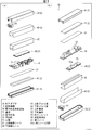
- FIG. 1A is an exploded perspective view showing the configuration of the heat dissipation mechanism 2 of the AC adapter 1A as the electronic apparatus according to the first embodiment, as viewed from the lower side of the AC adapter 1A.
- FIG. 1B shows the configuration of the heat dissipation mechanism 2 of the AC adapter 1A, and is an exploded perspective view of the AC adapter 1A as viewed from above.
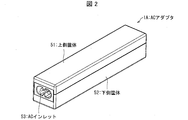
- FIG. 2 is a perspective view showing the configuration of the AC adapter 1A of the present embodiment.
- An AC (alternating current) alternating current (AC) adapter which is a power supply device as an electronic apparatus of the present embodiment, supplies power to, for example, a portable terminal that operates with a direct current (DC) power source. This is for converting the voltage into a DC voltage. For this reason, as shown in FIG. 2, an AC inlet 53 for connecting a cable (not shown) from an AC power source (not shown) is provided at one end of the AC adapter 1A. On the other hand, a DC cable for connecting to the portable terminal (not shown) is connected to the other end facing the one end of the AC adapter 1A.
- the AC adapter 1A of the present embodiment has, for example, an output of 65W (19V, 3.42A), a width of 26 mm, a length of 131 mm, a height of 25 mm, and a volume of about 85 cc. It has a shape.
- the general size of a conventional 65 W output AC adapter is, for example, 46 mm wide, 107.5 mm long, 29.6 mm high, and has a volume of about 150 cc.
- the AC adapter 1A of the present embodiment has a volume reduction of about 40% with the same output capacity as compared with the conventional product. Further, if the volume is reduced, the upper casing 51 and the lower casing 52 which are casings are also reduced, and the weight can be reduced. For this reason, even if it puts in a bag, it has the merit that it is not bulky.
- an AC (alternating current) adapter 1A that is a power supply device as an electronic device is illustrated, but in the present invention, the electronic device and the power supply device are not necessarily limited to the AC adapter 1A.
- another device such as a built-in power source for a desktop PC or a built-in power source for a TV may be used.
- FIG. 2 shows an example in which the stick shape is 85 cc and the aspect ratio between the width and the length is 5 or more.
- the shape has a width of 35 mm, a length of 96 mm, and a height of 25 mm.
- the aspect ratio between the width and the length may be 3 or less.
- the AC adapter 1 ⁇ / b> A covers an electronic component mounting substrate 10 in which a plurality of electronic components 12 are mounted on a substrate 11 by soldering, and covers the electronic component mounting substrate 10.
- An upper housing 51 and a lower housing 52 are provided as housings.
- an upper insulating sheet 31 that covers the electronic component mounting substrate 10 from the upper side an upper aluminum plate 41 that covers the upper insulating sheet 31 from the upper side, and an upper aluminum plate 41 that is on the upper side
- the upper casing 51 that covers from above.
- a molding filler 20 on the lower side of the electronic component mounting substrate 10, a molding filler 20, a lower insulating sheet 32 that covers the molding filler 20 from the lower side, and a rear surface side heat dissipation metal that covers the lower insulating sheet 32 from the lower side.
- a lower aluminum plate 42 as a plate and a lower housing 52 that covers the lower aluminum plate 42 from below are provided.
- the AC inlet 53 mentioned above is provided in the edge part of AC adapter 1A.
- the upper insulating sheet 31 and the lower insulating sheet 32 are a pair of two, for example, polycarbonate resin or hard paper.
- the lower insulating sheet 32 has a C channel cross section and covers the periphery of the electronic component mounting board 10.
- the upper insulating sheet 31 is a flat sheet and covers the upper surface of the lower insulating sheet 32.
- the shapes of the upper insulating sheet 31 and the lower insulating sheet 32 are not necessarily limited thereto, and the upper insulating sheet 31 may have a C-channel cross section, while the lower insulating sheet 32 may be a flat sheet.
- An upper aluminum plate 41 and a lower aluminum plate 42 are provided on the outer portions of the upper insulating sheet 31 and the lower insulating sheet 32.
- the upper aluminum plate 41 and the lower aluminum plate 42 are a pair of two, and are made of an aluminum material as a metal material having good thermal conductivity. Accordingly, the heat generated from the electronic component 12 of the electronic component mounting substrate 10 serves as a heat radiating fin by using the upper aluminum plate 41 and the lower aluminum plate 42 which are materials having good conductivity. ing.
- an aluminum material is used as a metal material.
- the present invention is not limited to this, and a material such as a copper plate as a metal material having good thermal conductivity can also be used.
- the upper housing 51 and the lower housing 52 form a pair of two, and each is formed in a box shape with resin. Therefore, when the upper housing 51 and the lower housing 52 are integrally combined, the electronic component mounting substrate 10 is completely accommodated.
- FIG. 3A is a rear view showing the configuration of the electronic component mounting board 10 in the AC adapter 1A.
- FIG. 3B is a plan view showing the configuration of the electronic component mounting board 10.
- FIG. 3C is a left side view showing the configuration of the electronic component mounting board 10.
- FIG. 3D is a front view showing the configuration of the electronic component mounting board 10.
- FIG. 3E is a right side view showing the configuration of the electronic component mounting board 10.
- FIG. 3F is a bottom view showing the configuration of the electronic component mounting board 10.
- the electronic component mounting substrate 10 includes a substrate 11 and a plurality of electronic components 12 mounted on the surface of the substrate 11 by soldering.
- the electronic component 12 mounted on the surface of the substrate 11 is composed of, for example, a transformer, an axial resistor, an electrolytic capacitor, and the like.
- the electronic component 12 is not necessarily limited to this, and may be another component.
- soldering portion for connecting the lead of the electronic component 12 mounted on the front surface of the substrate 11 on the back surface of the substrate 11 is formed on the back surface of the substrate 11, and an FET (Field effect transistor: Surface mount components such as field effect transistors or bridge diodes are provided.
- FET Field effect transistor: Surface mount components such as field effect transistors or bridge diodes are provided.
- the soldering portion and the surface mounting component are the protruding portions 13 protruding from the substrate 11. Accordingly, the plurality of protrusions 13 have different shapes and sizes depending on each surface-mounted component mounted on the back surface of the substrate 11.
- the FET is a lead package such as a three-terminal regulator TO (TransistorlineOutline) 220 package, and includes a heat radiation fin made of aluminum (Al) or copper (Cu).
- the electronic component mounting substrate 10 in the AC adapter 1A of the present embodiment is a small one, and the FET is made of a TO252 package. Therefore, FET (Field effect transistor) or bridge diode is a surface mount component. As a result, in the electronic component mounting substrate 10 of the present embodiment, heat is radiated by the substrate 11.
- the three-terminal regulator TO (Transistor-Outline) 220 package is a type of package in which a radiator is provided on the opposite side of the TO-based, that is, plastic-based lead.
- the TO252 package is a TO system, that is, a plastic system, but is thin and can be surface-mounted.
- FIG. 4A is a cross-sectional view showing the configuration of the electronic component mounting board 10 and the molding filler 20 in the AC adapter 1A.
- FIG. 4B is a cross-sectional view illustrating configurations of an electronic component mounting board and a heat dissipation sheet in a conventional electronic device.
- the heat dissipation mechanism 2 includes the molded filler 20, the lower aluminum plate 42 and the upper aluminum plate 41, and the lower casing 52 and the upper casing 51.
- FIG. 4A there is a gap portion 3 made of an air layer between the back surface of the electronic component mounting substrate 10 and the lower aluminum plate 42. Filling with a filler is preferable from the viewpoint of heat conduction. That is, it is preferable to reduce the thermal resistance between the back surface of the electronic component mounting substrate 10 and the lower aluminum plate 42.
- the molded filler 20 as the filler protrudes including a plurality of soldering portions. It has a hole 21 matched with the shape and size of the part 13.
- the molding filler 20 is made of, for example, a resin material such as epoxy resin, polycarbonate resin, or acrylic resin, and is a flat plate that matches the planar shape of the electronic component mounting substrate 10. Moreover, it does not ask
- the molding filler 20 is not composed of a plurality of members, the molding filler 20 can be easily inserted into the gap 3 at one time. As a result, it does not take time for positioning, so the man-hour is not increased. Moreover, it does not forget to put a part of the plurality of pieces.
- the molding filler 20 is molded with a hole 21 that matches the shape of the protruding portion 13. Therefore, the desired gap 3 is set to be filled with the molding filler 20.
- the molding filler 20 is not filled into the necessary portion of the gap 3 as in the case of inserting a granular or massive filler having elasticity or plasticity that is deformed when pressure is applied.
- the filling amount of the molding filler 20 is always an appropriate amount, and there is no characteristic variation due to excessive or insufficient filling.
- the hole 21 is put on the protrusion 13, the positioning of the hole 21 is easy.
- the AC adapter that can efficiently fill the molding filler 20 in the gap 3 between the back surface of the electronic component mounting substrate 10 on which the protruding portions 13 including the plurality of soldering portions are formed and the lower aluminum plate 42. 1A of heat dissipation mechanism 2 can be provided.
- the molded filler 20 has elasticity or plasticity that is deformed when pressed by the protruding portion 13.
- the molding filler 20 can be made of a rubber material such as silicone rubber or butadiene rubber.
- the protrusions 13 such as the surface mount components may vary in height or mounting position.
- the molding filler 20 is deformed when pressed by the protruding portion 13, the molding filler 20 is deformed and can be inserted.
- the adhesion between the protruding portion 13 and the hole 21 of the molded filler 20 is increased, and the heat dissipation effect is increased.
- the back side heat dissipation metal plate is made of an aluminum plate. Therefore, since the aluminum plate has high thermal conductivity, the heat generated in the electronic component 12 mounted on the electronic component mounting substrate 10 is transferred to the lower side through the lower aluminum plate 42 and the upper aluminum plate 41 made of the aluminum plate. Heat can be efficiently dissipated to the casing 52 and the upper casing 51.
- the AC adapter 1A as the power supply device in the present embodiment includes the heat dissipation mechanism 2 of the present embodiment.
- a heat dissipation mechanism capable of efficiently filling the molding filler 20 into the gap 3 between the back surface of the electronic component mounting substrate 10 on which the protruding portions 13 including a plurality of soldering portions are formed and the lower aluminum plate 42.
- the AC adapter 1 ⁇ / b> A as a power supply device including 2 can be provided.
- the molded filler 20 is configured by one piece.
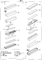
- the heat dissipation mechanism 2 of the AC adapter 1B as the electronic apparatus of the present embodiment is molded and filled as shown in FIGS. 5 (a) and 5 (b) and FIGS. 6 (a) to 6 (e).
- the material 60 is different in that the material 60 is made of a layered sheet-like material.
- FIG. 5A shows the configuration of the heat dissipation mechanism 2 of the AC adapter 1B in the present embodiment, and is an exploded perspective view of the AC adapter 1B as viewed from below.
- FIG. 5B shows the structure of the heat dissipation mechanism 2 of the AC adapter 1B, and is an exploded perspective view of the AC adapter 1B as viewed from above.
- FIGS. 6A to 6E are plan views showing configurations of the first sheet 61 to the fifth sheet 65 in the molding filler 60 of the AC adapter 1B.
- a molded filler as a filler.
- Reference numeral 60 is made of a sheet material stacked in layers.
- the protrusion 13 such as the surface mounting component mounted on the back surface of the electronic component mounting substrate 10 has a complicated unevenness in the height direction. There is. In that case, it is difficult to form the hole 21 having unevenness in a complicated manner in the height direction with the molding filler 20 of Embodiment 1 composed of one piece.
- the molding filler 60 of the present embodiment is formed by laminating the first sheet 61 to the fifth sheet 65 as sheet-like materials. ing.
- Each of the first sheet 61 to the fifth sheet 64 has a first sheet hole in accordance with the shape of the protrusion 13 such as the surface mounting component mounted on the back surface of the electronic component mounting substrate 10 in the height direction.
- a portion 61a, a second sheet hole 62a, a third sheet hole 63, and a fourth sheet hole 64a are formed.
- the first sheet hole portion 61a, the second sheet hole portion 62a, the third sheet hole portion 63, and the fourth sheet hole portion 64a of each of the first sheet 61 to the fifth sheet 64 are the protruding portions 13 at the height positions where they overlap.
- the die is molded according to the shape including the size.
- the first sheet 61 to the fifth sheet 65 are sequentially stacked on the back surface of the electronic component mounting substrate 10.
- the protruding portion 13 such as the surface mounting component mounted on the back surface of the electronic component mounting substrate 10 has a complicated unevenness in the height direction, it protrudes for each of the first sheet 61 to the fifth sheet 64.
- the first sheet hole 61a, the second sheet hole 62a, the third sheet hole 63, and the fourth sheet hole 64a can be easily formed according to the shape of the portion 13.
- the present invention when the molding filler 60 is inserted into the gap 3, the first sheet 61 to the fifth sheet 65 are sequentially stacked on the back surface of the electronic component mounting board 10.
- the present invention is not necessarily limited to this, and it is possible to insert the first sheet 61 to the fifth sheet 65, which are previously stacked and integrated with an adhesive or the like, at a time.
- each of the first sheet 61 to the fifth sheet 65 is made of a material having elasticity or plasticity that is deformed when pressed by the protruding portion 13.
- the first sheet 61 to the fifth sheet 65 can be made of a rubber-based material such as silicone rubber or butadiene rubber.
- the height of the protrusions 13 of the surface mount components and the attachment position may vary. obtain.
- the first sheet 61 to the fifth sheet 65 of the molded filler 60 are deformed as long as the molded filler 60 has elasticity or plasticity that is deformed when pressed by the protruding portion 13. Thus, it can be easily inserted into the gap 3 in which the protrusion 13 is formed.
- the heat dissipation mechanism 2 of the electronic device includes an electronic component mounting substrate 10 in which the electronic component 12 is mounted on the substrate 11, and a housing that houses the electronic component mounting substrate 10.
- a back side heat radiating metal plate (lower side aluminum plate 42) covering at least the back side of the electronic component mounting board 10, and a plurality of The protrusion 13 is inserted into the gap 3 between the back surface of the electronic component mounting substrate 10 on which the protrusion 13 including the soldered portion is formed and the back surface side heat radiating metal plate (lower aluminum plate 42). It is characterized by comprising a filler (molded filler 20) molded with a hole 21 matched to the shape.
- the filler is formed by molding with a hole that matches the shape of the protruding portion including a plurality of soldered portions. For this reason, even if the protrusions having various shapes and sizes exist, the electronic component mounting board on which the protrusions including a plurality of soldering parts are formed can be simply covered with the filler on the back surface of the electronic component mounting board. A filler can be inserted and filled in the gap between the back surface and the backside heat radiating metal plate.
- the filler does not consist of a plurality of members, the filler can be easily inserted and filled in the gap portion at one time. As a result, it does not take time for positioning, so the man-hour is not increased.
- the filler is molded with a hole that matches the shape of the protrusion. For this reason, it sets so that a desired clearance gap may be filled with a filler. As a result, unlike the case where a granular or lump filler that is deformed when pressure is applied is inserted, a necessary portion of the gap is not filled with the filler.
- a heat dissipation mechanism for an electronic device that can efficiently fill the gap between the back surface of the electronic component mounting board on which the protrusions including the plurality of soldering portions are formed and the back surface side heat radiating metal plate. be able to.
- the heat dissipating mechanism 2 of the electronic device (AC adapter 1A / AC adapter 1B) according to aspect 2 of the present invention is the heat dissipating mechanism of the electronic device according to aspect 1, wherein the filler (molded filler 20 / molded filler 60) is It is preferable to be deformed when pressed by the protrusion 13.
- the protruding portion of the surface mounting component or the like may vary in height or mounting position.
- the filler can be easily inserted by being deformed.
- the heat dissipating mechanism 2 of the electronic device (AC adapter 1B) in aspect 3 of the present invention is the heat dissipating mechanism of the electronic device in aspect 1 or 2, wherein the filler (molded filler 60) is a sheet-like material (first sheet 61). To the fifth sheet 65), and each sheet-like material (first sheet 61 to fifth sheet 65) is shaped according to the shape of the protruding portion 13 at the height of the sheet. It is preferable that the sheet is punched (one sheet hole 61a, second sheet hole 62a, third sheet hole 63, fourth sheet hole 64a).
- the heat dissipating mechanism 2 of the electronic device (AC adapter 1A / AC adapter 1B) according to aspect 4 of the present invention is the heat dissipating mechanism of the electronic device according to aspect 1, 2, or 3, wherein the back surface heat dissipating metal plate (lower aluminum plate 42) Is preferably made of an aluminum plate.
- the aluminum plate has high thermal conductivity, so the heat generated by the electronic components mounted on the electronic component mounting board can be efficiently dissipated to the housing via the backside heat dissipation metal plate made of aluminum plate. Can do.
- a power supply device (AC adapter 1A / AC adapter 1B) according to aspect 5 of the present invention includes the heat dissipation mechanism 2 for an electronic device according to any one of aspects 1 to 4.
- an electronic device that can efficiently fill the gap between the back surface of the electronic component mounting board on which the protruding portion including the plurality of soldering portions is formed and the heat radiation metal plate on the back surface can be efficiently filled.
- a power supply device including a heat dissipation mechanism can be provided.
- the present invention can be applied to an electronic device including an electronic component mounting board in which an electronic component is mounted on a board, and a housing that houses the electronic component mounting board. Moreover, as an electronic device, it can apply to power supply devices, such as an AC adapter and a switching power supply circuit, for example.
Landscapes
- Engineering & Computer Science (AREA)
- Microelectronics & Electronic Packaging (AREA)
- Physics & Mathematics (AREA)
- Thermal Sciences (AREA)
- Cooling Or The Like Of Electrical Apparatus (AREA)
- Cooling Or The Like Of Semiconductors Or Solid State Devices (AREA)
Abstract
本発明のACアダプタ(1A)は、基板(11)に電子部品(12)を実装した電子部品実装基板(10)と、電子部品実装基板(10)を収納する上側筐体(51)及び下側筐体(52)とを備える。放熱機構(2)は、電子部品実装基板(10)の少なくとも裏面を覆う下側アルミ板(42)と、複数の半田付け部を含む突出部(13)が形成された電子部品実装基板(10)の裏面と下側アルミ板(42)との間の隙間部に挿入すべく、突出部(13)の形状に合わせた穴部(21)を有して成型された成型充填材(20)とを備えている。
Description
本発明は、基板に電子部品を実装した電子部品実装基板と、上記電子部品実装基板を収納する筐体とを備えた電子機器の放熱機構及び電源装置に関するものである。
ACアダプタ等の電源装置は、一般的に所定の交流電圧を所望の直流(DC:Direct Current)電圧に変換する役割をする。尚、日本では、交流電圧の実効値(RMS:Root Mean Square value)は100Vである。また、例えばノートパソコン(PC:Personal Computer)に供給する所望の直流電圧は19Vである。
上記のACアダプタは、ノートパソコン等において外部電源として使用される。近年、モバイルパソコンやタブレットパソコンの普及により、カバンに入れても邪魔にならないACアダプタの小型化のニーズが高まっている。
通常、ACアダプタは、バイポーラトランジスタやMOS-FET(Metal Oxide Semiconductor Field Effect Transistor:金属酸化物半導体電界効果トランジスタ)を備え、スイッチング動作を行う。また、ACアダプタは、ダイオードを備え、アノード及びカソード両端子の電位で決まる整流動作を行う。
さらに、ACアダプタは、交流電圧を全波整流するためにブリッジダイオードを備えている。
これらの半導体は、スイッチングによる電力損失(スイッチング損失)と、電流を流すことによる電力損失(導通損失)とを発生させる。そして、これらの損失は、半導体の発熱の原因となり、その結果、ACアダプタが発熱する。
半導体のジャンクション温度、つまり半導体の接合部温度の上昇は、半導体の寿命を短くする。また、半導体の発熱によって近接の電解コンデンサの温度が上昇すると、電解コンデンサの寿命が短くなり、その結果、ACアダプタの寿命が短くなる。そこで、冷却手段が必要となる。
ここで、従来の電子機器における冷却手段として、例えば、図7の(a)(b)に示す電子部品の半田面の部品を冷却する一例が知られている。
すなわち、従来の電子機器としての一例としての例えばACアダプタ100は、図7の(a)(b)に示すように、基板111には種々の電子部品112が半田付けにて固定された電子部品実装基板110を備えている。ここで、リードタイプの足の形状の部品(例えばアキシャル抵抗器、大型電解コンデンサ、トランス、コモンチョークコイル、又は半導体のTO-220パッケージ等)は、図7(b)に示す電子部品実装基板110の上側に実装して、裏面からリードを半田付けする。また、面実装タイプの部品(チップ抵抗器、チップコンデンサ、又は半導体のTO-252パッケージ等)は、裏面に実装して、裏面にて半田付けする。したがって、基板111の裏面は、半田付けしたリードの他、該基板111の裏面に実装した面実装部品が存在する。面実装部品の形状は部品によって異なるため、複数の突出部113…に示すように、各突出部113の高さは、基板111の裏面に実装される該突出部113に含まれる面実装部品の種類によって異なる。
そこで、従来のACアダプタ100では、複数の電子部品から発生する熱を基板111の裏面から放熱するために、放熱シート121~124を部分毎に切り出し、かつ重ねて使用している。
このように、半導体等の発熱部品からの熱を、基板111に伝えずにアルミ板140及び筐体150に効果的に伝えることによって、基板111を冷却している。
上記ACアダプタ100においては、半田部温度の上昇及び冷熱のヒートショックが、半田部のクラックの原因となり、延いては発火等の事故に至る場合があるが、上記冷却機構にて回避できるようになっている。
しかしながら、上記従来の冷却機構では、放熱シート121~124を別々のパーツにて構成するため、位置決めに時間を要し、各々を組み立てる工数が増加するので、製造コストが増大する。また、組み忘れが発生した場合には、製品の品質にも影響するという問題点を有している。
ここで、従来の冷却機構の他の方法として、例えば、特許文献1に開示された電子部品一体モールド構造を有する電気・電子モジュールにて知られているように、樹脂や粘度の低いグリースを隙間に注入するという方法がある。
しかしながら、樹脂や粘度の低いグリースを隙間に注入する方法では、所望の位置へ注入するためには壁等の構造物が必要となる。また、作業員によって樹脂やグリースを注入する量が変化するので、特に、注入規定量に対して注入量が不足する場合には、冷却能力が低減する。
また、樹脂やグリースを注入した場合、硬化時間が必要となるので、組立時間が長くなり、量産に支障を来すという問題点を有している。
さらに、他の従来の冷却機構として、圧力をかけると変形する弾性又は塑性を有する顆粒状又は塊状の充填材を適量挿入して、基板への挿入時にその圧力にて充填材を変形させる方法がある。
しかしながら、その方法では、事前の挿入量と基板組み込みの圧力とによって、必要な隙間に入り込まなかったり、逆に不要な部分にも広がってしまったりするという問題点を有している。また、弾性又は塑性を有する充填材の比重が重い場合は、挿入量のばらつきにより組み立てた電子機器の重量にばらつきが生じるという問題点を有している。
本発明は、上記従来の問題点に鑑みなされたものであって、その目的は、複数の半田付け部を含む突出部が形成された電子部品実装基板の裏面と裏面側放熱金属板との間の隙間部に効率よく充填材を充填し得る電子機器の放熱機構及び電源装置を提供することにある。
本発明の一態様における電子機器の放熱機構は、上記課題を解決するために、基板に電子部品を実装した電子部品実装基板と、上記電子部品実装基板を収納する筐体とを備えた電子機器の放熱機構において、上記電子部品実装基板の少なくとも裏面を覆う裏面側放熱金属板と、複数の半田付け部を含む突出部が形成された上記電子部品実装基板の裏面と上記裏面側放熱金属板との間の隙間部に挿入すべく、該突出部の形状に合わせた穴部を有して成型された充填材とを備えていることを特徴としている。
また、本発明の一態様における電源装置は、上記課題を解決するために、前記記載の電子機器の放熱機構を備えていることを特徴としている。
本発明の一態様によれば、複数の半田付け部を含む突出部が形成された電子部品実装基板の裏面と裏面側放熱金属板との間の隙間部に効率よく充填材を充填し得る電子機器の放熱機構及び電源装置を提供するという効果を奏する。
〔実施の形態1〕
本発明の一実施形態について図1~図4に基づいて説明すれば、以下のとおりである。
本発明の一実施形態について図1~図4に基づいて説明すれば、以下のとおりである。
(電子機器の構成)
本実施の形態における電子機器の放熱機構について、図1の(a)(b)及び図2に基づいて説明する。図1の(a)は、本実施の形態1における電子機器としてのACアダプタ1Aの放熱機構2の構成を示すものであってACアダプタ1Aを下側から見た分解斜視図である。図1の(b)は、ACアダプタ1Aの放熱機構2の構成を示すものであってACアダプタ1Aを上側から見た分解斜視図である。図2は、本実施の形態のACアダプタ1Aの構成を示す斜視図である。
本実施の形態における電子機器の放熱機構について、図1の(a)(b)及び図2に基づいて説明する。図1の(a)は、本実施の形態1における電子機器としてのACアダプタ1Aの放熱機構2の構成を示すものであってACアダプタ1Aを下側から見た分解斜視図である。図1の(b)は、ACアダプタ1Aの放熱機構2の構成を示すものであってACアダプタ1Aを上側から見た分解斜視図である。図2は、本実施の形態のACアダプタ1Aの構成を示す斜視図である。
本実施の形態の電子機器としての電源装置であるAC(alternating current:交流)アダプタは、DC(Direct Current :直流)電源にて稼動する例えば携帯端末に電力を供給するものであり、商用のAC電圧をDC電圧に変換するためのものである。このため、ACアダプタ1Aの一方の端部には、図2に示すように、図示しないAC電源からの図示しないケーブルを接続するためのACインレット53が設けられている。一方、ACアダプタ1Aの一方の端部に対向する他方の端部には、図示しない上記携帯端末に接続するためのDCケーブルが接続されるようになっている。
本実施の形態のACアダプタ1Aは、例えば出力が65W(19V、3.42A)となっており、幅26mm、長さ131mm、高さ25mmの大きさを有し、かつ容積が約85ccの直方体形状にてなっている。ここで、従来品の65W出力のACアダプタの一般的な大きさは、例えば幅46mm、長さ107.5mm、高さ29.6mmであり、かつ容積が約150ccにてなっている。このため、本実施の形態のACアダプタ1Aは、従来品に比べて同じ出力容量では約40%の体積減のものとなっている。また、体積が減れば、筐体である上側筐体51及び下側筐体52も小さくなり、軽量化が図れる。このため、カバンに入れても嵩張らないというメリットを有している。
尚、本実施の形態では、電子機器としての電源装置であるAC(alternating current:交流)アダプタ1Aを例示しているが、本発明においては、電子機器及び電源装置は必ずしもACアダプタ1Aに限らず、例えばデスクトップ型PCの内蔵電源や、TV用の内蔵電源等の他の装置であってもよい。また、図2においては、85ccのスティック形状であって、かつ幅と長さとのアスペクト比が5以上の場合の例を示したが、例えば幅35mm、長さ96mm、高さ25mmの形状のような、幅と長さとのアスペクト比が3以下の場合でもよい。
上記ACアダプタ1Aは、図1(a)(b)に示すように、基板11に複数の電子部品12が半田付けにて実装された電子部品実装基板10と、この電子部品実装基板10を覆う筐体としての上側筐体51と下側筐体52とを備えている。
詳細には、電子部品実装基板10の上側には、該電子部品実装基板10を上側から覆う上側絶縁シート31と、上側絶縁シート31を上側から覆う上側アルミ板41と、上側アルミ板41を上側から覆う上記上側筐体51とを備えている。
一方、電子部品実装基板10の下側には、成型充填材20と、該成型充填材20を下側から覆う下側絶縁シート32と、下側絶縁シート32を下側から覆う裏面側放熱金属板としての下側アルミ板42と、下側アルミ板42を下側から覆う下側筐体52とを備えている。そして、ACアダプタ1Aの端部には、前述したACインレット53が設けられている。
上記上側絶縁シート31及び下側絶縁シート32は、2つで一対となっており、例えば、ポリカーボネートの樹脂や硬質の紙にてなっている。本実施の形態では、下側絶縁シート32は断面Cチャネル形状にてなっており、電子部品実装基板10の周囲を覆うようになっている。一方、上側絶縁シート31は平面シートからなっており、下側絶縁シート32の上面を覆うようになっている。これにより、導電性を有する上側アルミ板41及び下側アルミ板42にて電子部品実装基板10を覆っても、電子部品実装基板10と上側アルミ板41及び下側アルミ板42との電気的絶縁が図れるようになっている。尚、上側絶縁シート31及び下側絶縁シート32の形状は、必ずしもこれに限らず、上側絶縁シート31が断面Cチャネル形状である一方、下側絶縁シート32が平面シートであってもよい。
上記上側絶縁シート31及び下側絶縁シート32の外側部分には、上側アルミ板41及び下側アルミ板42が設けられている。これら上側アルミ板41及び下側アルミ板42は、2つで一対となっており、熱伝導性のよい金属材料としてのアルミ材にて構成されている。これにより、電子部品実装基板10の電子部品12から発生される熱を、伝導性のよい材料である上側アルミ板41及び下側アルミ板42を用いることにより、放熱フィンの役割を果たすものとなっている。
尚、本実施の形態では、金属材料としてのアルミ材が使用されているが、必ずしもこれに限らず、熱伝導性のよい金属材料としての例えば銅板等の材料を用いることも可能である。
上側筐体51及び下側筐体52は、2つで一対となっており、それぞれが樹脂にて箱状に形成されている。したがって、上側筐体51と下側筐体52とが一体的に合わされることによって、電子部品実装基板10が完全に収容された状態となる。
次に、上記電子部品実装基板10の構成について、図3の(a)~(f)に基づいて説明する。図3の(a)は、ACアダプタ1Aにおける電子部品実装基板10の構成を示す背面図である。図3の(b)は、電子部品実装基板10の構成を示す平面図である。図3の(c)は、電子部品実装基板10の構成を示す左側面図である。図3の(d)は、電子部品実装基板10の構成を示す正面図である。図3の(e)は、電子部品実装基板10の構成を示す右側面図である。図3の(f)は、電子部品実装基板10の構成を示す底面図である。
上記電子部品実装基板10は、図3の(a)~(f)に示すように、基板11とこの基板11の表面に半田付けにて実装された複数の電子部品12…とを備えている。これら基板11の表面に搭載された電子部品12は、例えばトランス、アキシャル抵抗、電解コンデンサ等からなっている。ただし、電子部品12は必ずしもこれに限らず、他の部品であってもよい。
一方、基板11の裏面には、上記基板11の表面に搭載された電子部品12のリードを、基板11の裏面で接続するための半田付け部が形成されていると共に、FET(Field effect transistor:電界効果トランジスタ)又はブリッジダイオード等の面実装部品が設けられている。この結果、上記半田付け部及び面実装部品は、基板11に対して突出する突出部13となっている。したがって、複数の突出部13…は、基板11の裏面に実装された各面実装部品によって、互いに異なる形状及び大きさを有している。
すなわち、従来の大型の電子部品実装基板では、FETは3端子レギュレータTO(Transistor Outline)220パッケージ等のリードパッケージにてなっており、アルミニウム(Al)や銅(Cu)からなる放熱フィンを備えている。しかし、本実施の形態のACアダプタ1Aにおける電子部品実装基板10は、小型のものであり、FETはTO252パッケージからなっている。したがって、FET(Field effect transistor:電界効果トランジスタ)又はブリッジダイオードは、面実装部品となっている。この結果、本実施の形態の電子部品実装基板10では、基板11にて放熱するようになっている。尚、3端子レギュレータTO(Transistor Outline)220パッケージは、TO系つまりプラスチック系のリードの反対側に放熱器を設けているタイプのパッケージである。一方、TO252パッケージは、TO系つまりプラスチック系であるが、薄型であり、面実装可能となっている。
(電子機器の放熱機構の構成)
次に、上記構成を備えたACアダプタ1Aにおける放熱機構2の構成について、図1の(a)(b)及び図4の(a)(b)に基づいて説明する。図4の(a)は、ACアダプタ1Aにおける電子部品実装基板10及び成型充填材20の構成を示す断面図である。図4の(b)は、従来の電子機器における電子部品実装基板及び放熱シートの構成を示す断面図である。
次に、上記構成を備えたACアダプタ1Aにおける放熱機構2の構成について、図1の(a)(b)及び図4の(a)(b)に基づいて説明する。図4の(a)は、ACアダプタ1Aにおける電子部品実装基板10及び成型充填材20の構成を示す断面図である。図4の(b)は、従来の電子機器における電子部品実装基板及び放熱シートの構成を示す断面図である。
尚、本実施の形態では、放熱機構2は、成型充填材20、下側アルミ板42及び上側アルミ板41、並びに下側筐体52及び上側筐体51にて構成されている。
先ず、前述したように、本実施の形態のACアダプタ1Aでは、基板11に電子部品12を実装した電子部品実装基板10と、電子部品実装基板10を収納する上側筐体51及び下側筐体52とを備えている。また、電子部品実装基板10の裏面には、該電子部品実装基板10の少なくとも裏面を覆う下側アルミ板42が設けられている。
このようなACアダプタ1Aでは、電子部品実装基板10に実装されている電子部品12等から熱が発生する。このため、複数の突出部13…が形成された電子部品実装基板10の裏面側から熱を放散し、下側絶縁シート32及び上側絶縁シート31、並びに下側アルミ板42及び上側アルミ板41を介して下側筐体52及び上側筐体51に熱を逃がす必要がある。尚、下側筐体52及び上側筐体51は、放射と対流とにより熱をACアダプタ1Aの外部の大気に逃がす。
この場合、電子部品実装基板10の裏面と下側アルミ板42との間には、図4の(a)に示すように、空気層からなる隙間部3が存在するので、この隙間部3を充填材にて充填することが熱伝導の点から好ましい。すなわち、電子部品実装基板10の裏面と下側アルミ板42との熱抵抗を減らすことが好ましい。
しかしながら、電子部品実装基板10の裏面には、複数の半田付け部だけでなく該裏面に実装される面実装部品等の突出部13が存在する。そして、これら突出部13…は、形状及び大きさが様々である。
このため、従来では、図4の(b)に示すように、隙間部103を充填材にて充填する場合に、例えば、放熱シート121~124を突出部113の形状及び大きさ毎に切り出し、かつ重ねて使用していた。このため、位置決めに時間を要し、工数の増加を招いていた。また、充填材として、グリース等を注入する場合には、壁等の構造物が必要であり、かつ硬化時間が必要であるので、組立時間が長くなる等の問題を有していた。さらに、圧力をかけると変形する弾性又は塑性を有する顆粒状又は塊状の充填材を挿入する場合には、必要な隙間部に入り込まないことがあった。
これに対して、本実施の形態では、図1の(a)(b)及び図4の(a)に示すように、充填材としての成型充填材20を、複数の半田付け部を含む突出部13…の形状及び大きさに合わせた穴部21…を有して成型して構成している。この成型充填材20は、例えば、エポキシ樹脂、ポリカーボネート樹脂又はアクリル樹脂等の樹脂系材料にてなっており電子部品実装基板10の平面形状に合わせた平板にてなっている。また、穴部21…は、貫通しているか否かを問わない。
この結果、種々の形状及び大きさを有する突出部13…が存在しても、成型充填材20を電子部品実装基板10の裏面に被せるだけで、複数の半田付け部を含む突出部13が形成された電子部品実装基板10の裏面と下側アルミ板42との間の隙間部3に挿入して充填することができる。
それゆえ、成型充填材20が複数の部材からなるということがないので、一回で容易に隙間部3に成型充填材20を挿入することができる。この結果、位置決めに時間を要することもないので、工数の増加を招くことがない。また、複数のピースのうちの一部を入れ忘れるということもない。
また、成型充填材20は、突出部13の形状に合わせた穴部21を有して成型されている。このため、所望の隙間部3には成型充填材20が充填されるように設定されている。この結果、圧力をかけると変形する弾性又は塑性を有する顆粒状又は塊状の充填材を挿入する場合のように、隙間部3の必要な部位に成型充填材20が充填されないということがない。また、成型充填材20の充填量が常に適量となり、入れ過ぎや不足による特性ばらつきがない。さらに、穴部21を突出部13に被せるときに、穴部21の位置決めも容易である。
したがって、複数の半田付け部を含む突出部13…が形成された電子部品実装基板10の裏面と下側アルミ板42との間の隙間部3に効率よく成型充填材20を充填し得るACアダプタ1Aの放熱機構2を提供することができる。
ここで、本実施の形態におけるACアダプタ1Aの放熱機構2では、成型充填材20は、突出部13に押圧されると変形する弾性又は塑性を有していることが好ましい。この場合、成型充填材20は、例えばシリコーンゴム又はブタジエンゴム等のゴム系材料にて構成することが可能である。
例えば、各電子部品実装基板10の裏面における面実装部品等の突出部13の取り付け精度等により、面実装部品等の突出部13に高さ変動や取り付け位置の変動があることが起こり得る。しかし、この場合においても、成型充填材20は、突出部13に押圧されると変形する場合には、成型充填材20が変形することにより、嵌挿可能となる。さらに、突出部13と成型充填材20の穴部21との密着性が増し、放熱効果が上がる。
また、本実施の形態におけるACアダプタ1Aの放熱機構2では、裏面側放熱金属板は、アルミ板からなっている。これにより、アルミ板は熱伝導性が高いので、電子部品実装基板10に実装された電子部品12にて発生した熱をアルミ板からなる下側アルミ板42及び上側アルミ板41を介して下側筐体52及び上側筐体51へ効率よく熱放散することができる。
また、本実施の形態における電源装置としてのACアダプタ1Aは、本実施の形態の放熱機構2を備えている。この結果、複数の半田付け部を含む突出部13が形成された電子部品実装基板10の裏面と下側アルミ板42との間の隙間部3に効率よく成型充填材20を充填し得る放熱機構2を備えた電源装置としてのACアダプタ1Aを提供することができる。
〔実施の形態2〕
本発明の他の実施の形態について図5及び図6に基づいて説明すれば、以下のとおりである。尚、本実施の形態において説明すること以外の構成は、前記実施の形態1と同じである。また、説明の便宜上、前記の実施の形態1の図面に示した部材と同一の機能を有する部材については、同一の符号を付し、その説明を省略する。
本発明の他の実施の形態について図5及び図6に基づいて説明すれば、以下のとおりである。尚、本実施の形態において説明すること以外の構成は、前記実施の形態1と同じである。また、説明の便宜上、前記の実施の形態1の図面に示した部材と同一の機能を有する部材については、同一の符号を付し、その説明を省略する。
前記実施の形態1の電子機器としてのACアダプタ1Aの放熱機構2では、成型充填材20は、1つのピースにて構成されていた。これに対して、本実施の形態の電子機器としてのACアダプタ1Bの放熱機構2は、図5の(a)(b)及び図6の(a)~(e)に示すように、成型充填材60がシート状材料を層状に重ねたものからなって点が異なっている。
本実施の形態の電子機器としてのACアダプタ1Bの放熱機構2について、図5の(a)(b)及び図6の(a)~(e)に基づいて説明する。図5(a)は、本実施の形態におけるACアダプタ1Bの放熱機構2の構成を示すものであってACアダプタ1Bを下側から見た分解斜視図である。図5(b)は、ACアダプタ1Bの放熱機構2の構成を示すものであってACアダプタ1Bを上側から見た分解斜視図である。図6の(a)~(e)は、ACアダプタ1Bの成型充填材60における第1シート61~第5シート65の構成を示す平面図である。
本実施の形態における電子機器としてのACアダプタ1Bの放熱機構2では、図5の(a)(b)及び図6の(a)~(e)に示すように、充填材としての成型充填材60は、シート状材料を層状に重ねたものからなっている。
例えば、図5の(a)(b)に示すように、電子部品実装基板10の裏面に実装される面実装部品等の突出部13…には、高さ方向において複雑に凹凸している場合がある。その場合には、1つのピースからなる実施の形態1の成型充填材20では、高さ方向において複雑に凹凸を有する穴部21を形成することが困難である。
そこで、本実施の形態の成型充填材60は、図6の(a)~(e)に示すように、シート状材料としての第1シート61~第5シート65を層状に重ねたものからなっている。そして、各第1シート61~第5シート64には、電子部品実装基板10の裏面に実装される面実装部品等の突出部13の高さ方向に凹凸する形状に合わせて、第1シート穴部61a・第2シート穴部62a・第3シート穴部63・第4シート穴部64aがそれぞれ形成されている。これら各第1シート61~第5シート64の第1シート穴部61a・第2シート穴部62a・第3シート穴部63・第4シート穴部64aは、その重ねる高さ位置の突出部13の大きさを含む形状に応じて型抜き成型されている。
そして、前記複数の半田付け部を含む突出部13…が形成された電子部品実装基板10の裏面と下側アルミ板42との間の隙間部3に成型充填材60を挿入するときには、各第1シート61~第5シート65を順番に電子部品実装基板10の裏面に重ねていく。これにより、電子部品実装基板10の裏面に実装される面実装部品等の突出部13が高さ方向において複雑に凹凸を有していても、第1シート61~第5シート64毎に、突出部13の形状に応じた第1シート穴部61a・第2シート穴部62a・第3シート穴部63・第4シート穴部64aを容易に形成することができる。
ここで、本実施の形態では、隙間部3に成型充填材60を挿入するときには、各第1シート61~第5シート65を順番に電子部品実装基板10の裏面に重ねた。しかし、必ずしもこれに限らず、各第1シート61~第5シート65を、それぞれ予め重ねて接着剤等にて一体化したものを一回で挿入することが可能である。
この場合、各第1シート61~第5シート65を、突出部13に押圧されると変形する弾性又は塑性を有する材料にて構成しておくことが好ましい。この場合、第1シート61~第5シート65を、例えばシリコーンゴム又はブタジエンゴム等のゴム系材料にて構成しておくことが可能である。
これによって、各第1シート61~第5シート65を予め一体化しておいても、電子部品実装基板10の裏面に形成された突出部13に容易に嵌装することが可能となる。
すなわち、例えば、各電子部品実装基板10の裏面における面実装部品等の突出部13…の取り付け精度等により、面実装部品等の突出部13に高さ変動や取り付け位置の変動があることが起こり得る。しかし、この場合においても、成型充填材60は突出部13に押圧されると変形する弾性又は塑性を有していれば、成型充填材60の各第1シート61~第5シート65が変形することにより、該突出部13が形成された隙間部3に容易に嵌挿可能となる。
〔まとめ〕
本発明の態様1における電子機器(ACアダプタ1A・ACアダプタ1B)の放熱機構2は、基板11に電子部品12を実装した電子部品実装基板10と、上記電子部品実装基板10を収納する筐体(上側筐体51及び下側筐体52)とを備えた電子機器の放熱機構において、上記電子部品実装基板10の少なくとも裏面を覆う裏面側放熱金属板(下側アルミ板42)と、複数の半田付け部を含む突出部13が形成された上記電子部品実装基板10の裏面と上記裏面側放熱金属板(下側アルミ板42)との間の隙間部3に挿入すべく、該突出部13の形状に合わせた穴部21を有して成型された充填材(成型充填材20)とを備えていることを特徴としている。
本発明の態様1における電子機器(ACアダプタ1A・ACアダプタ1B)の放熱機構2は、基板11に電子部品12を実装した電子部品実装基板10と、上記電子部品実装基板10を収納する筐体(上側筐体51及び下側筐体52)とを備えた電子機器の放熱機構において、上記電子部品実装基板10の少なくとも裏面を覆う裏面側放熱金属板(下側アルミ板42)と、複数の半田付け部を含む突出部13が形成された上記電子部品実装基板10の裏面と上記裏面側放熱金属板(下側アルミ板42)との間の隙間部3に挿入すべく、該突出部13の形状に合わせた穴部21を有して成型された充填材(成型充填材20)とを備えていることを特徴としている。
上記発明によれば、充填材を、複数の半田付け部を含む突出部の形状に合わせた穴部を有して成型して構成している。このため、種々の形状及び大きさを有する突出部が存在しても充填材を電子部品実装基板の裏面に被せるだけで、複数の半田付け部を含む突出部が形成された電子部品実装基板の裏面と上記裏面側放熱金属板との間の隙間部に充填材を挿入して充填することができる。
このため、充填材が複数の部材からなるということがないので、一回で容易に隙間部に充填材を挿入して充填することができる。この結果、位置決めに時間を要することもないので、工数の増加を招くことがない。
また、充填材は、突出部の形状に合わせた穴部を有して成型されている。このため、所望の隙間部には充填材が充填されるように設定されている。この結果、圧力をかけると変形する顆粒状又は塊状の充填材を挿入する場合のように、隙間部の必要な部位に充填材が充填されないということがない。
したがって、複数の半田付け部を含む突出部が形成された電子部品実装基板の裏面と裏面側放熱金属板との間の隙間部に効率よく充填材を充填し得る電子機器の放熱機構を提供することができる。
本発明の態様2における電子機器(ACアダプタ1A・ACアダプタ1B)の放熱機構2は、態様1における電子機器の放熱機構において、前記充填材(成型充填材20・成型充填材60)は、前記突出部13に押圧されると変形することが好ましい。
例えば、各電子部品実装基板の裏面における電子部品の取り付け精度等により、面実装部品等の突出部に高さ変動や取り付け位置の変動があることが起こり得る。しかし、この場合においても、充填材は突出部に押圧されると変形するので、充填材が変形することにより、容易に嵌挿可能となる。
本発明の態様3における電子機器(ACアダプタ1B)の放熱機構2は、態様1又は2における電子機器の放熱機構において、前記充填材(成型充填材60)は、シート状材料(第1シート61~第5シート65)を層状に重ねたものからなっており、各シート状材料(第1シート61~第5シート65)は、その重ねる高さ位置の前記突出部13の形状に応じて型抜き(1シート穴部61a・第2シート穴部62a・第3シート穴部63・第4シート穴部64a)成型されていることが好ましい。
これにより、電子部品実装基板の裏面に実装される電子部品が高さ方向において複雑に凹凸を有していても、突出部の形状に応じた穴部を容易に形成することができる。
本発明の態様4における電子機器(ACアダプタ1A・ACアダプタ1B)の放熱機構2は、態様1、2又は3における電子機器の放熱機構において、前記裏面側放熱金属板(下側アルミ板42)は、アルミ板からなっていることが好ましい。
これにより、アルミ板は熱伝導性が高いので、電子部品実装基板に実装された電子部品にて発生した熱をアルミ板からなる裏面側放熱金属板を介して筐体へ効率よく熱放散することができる。
本発明の態様5における電源装置(ACアダプタ1A・ACアダプタ1B)は、態様1~4のいずれか1における電子機器の放熱機構2を備えていることを特徴としている。
上記の発明によれば、複数の半田付け部を含む突出部が形成された電子部品実装基板の裏面と裏面側放熱金属板との間の隙間部に効率よく充填材を充填し得る電子機器の放熱機構を備えた電源装置を提供することができる。
尚、本発明は、上述した各実施形態に限定されるものではなく、請求項に示した範囲で種々の変更が可能であり、異なる実施形態にそれぞれ開示された技術的手段を適宜組み合わせて得られる実施形態についても本発明の技術的範囲に含まれる。
本発明は、基板に電子部品を実装した電子部品実装基板と、電子部品実装基板を収納する筐体とを備えた電子機器に適用可能である。また、電子機器としては例えばACアダプタやスイッチング電源回路等の電源装置に適用することができる。
1A ACアダプタ(電子機器、電源装置)
1B ACアダプタ(電子機器、電源装置)
2 放熱機構
3 隙間部
10 電子部品実装基板
11 基板
12 電子部品
13 突出部
20 成型充填材
21 穴部
31 上側絶縁シート
32 下側絶縁シート
41 上側アルミ板
42 下側アルミ板(裏面側放熱金属板)
51 上側筐体
52 下側筐体
53 ACインレット
60 成型充填材
61 第1シート(シート状材料)
61a 第1シート穴部(穴部)
62 第2シート(シート状材料)
62a 第2シート穴部(穴部)
63 第3シート(シート状材料)
63a 第3シート穴部(穴部)
64 第4シート(シート状材料)
64a 第4シート穴部(穴部)
65 第5シート(シート状材料)
1B ACアダプタ(電子機器、電源装置)
2 放熱機構
3 隙間部
10 電子部品実装基板
11 基板
12 電子部品
13 突出部
20 成型充填材
21 穴部
31 上側絶縁シート
32 下側絶縁シート
41 上側アルミ板
42 下側アルミ板(裏面側放熱金属板)
51 上側筐体
52 下側筐体
53 ACインレット
60 成型充填材
61 第1シート(シート状材料)
61a 第1シート穴部(穴部)
62 第2シート(シート状材料)
62a 第2シート穴部(穴部)
63 第3シート(シート状材料)
63a 第3シート穴部(穴部)
64 第4シート(シート状材料)
64a 第4シート穴部(穴部)
65 第5シート(シート状材料)
Claims (5)
- 基板に電子部品を実装した電子部品実装基板と、上記電子部品実装基板を収納する筐体とを備えた電子機器の放熱機構において、
上記電子部品実装基板の少なくとも裏面を覆う裏面側放熱金属板と、
複数の半田付け部を含む突出部が形成された上記電子部品実装基板の裏面と上記裏面側放熱金属板との間の隙間部に挿入すべく、該突出部の形状に合わせた穴部を有して成型された充填材とを備えていることを特徴とする電子機器の放熱機構。 - 前記充填材は、前記突出部に押圧されると変形することを特徴とする請求項1記載の電子機器の放熱機構。
- 前記充填材は、シート状材料を層状に重ねたものからなっており、各シート状材料は、その重ねる高さ位置の前記突出部の形状に応じて型抜き成型されていることを特徴とする請求項1又は2記載の電子機器の放熱機構。
- 前記裏面側放熱金属板は、アルミ板からなっていることを特徴とする請求項1、2又は3記載の電子機器の放熱機構。
- 請求項1~4のいずれか1項に記載の電子機器の放熱機構を備えていることを特徴とする電源装置。
Applications Claiming Priority (2)
| Application Number | Priority Date | Filing Date | Title |
|---|---|---|---|
| JP2014066870 | 2014-03-27 | ||
| JP2014-066870 | 2014-03-27 |
Publications (1)
| Publication Number | Publication Date |
|---|---|
| WO2015146257A1 true WO2015146257A1 (ja) | 2015-10-01 |
Family
ID=54194799
Family Applications (1)
| Application Number | Title | Priority Date | Filing Date |
|---|---|---|---|
| PCT/JP2015/051713 Ceased WO2015146257A1 (ja) | 2014-03-27 | 2015-01-22 | 電子機器の放熱機構及び電源装置 |
Country Status (1)
| Country | Link |
|---|---|
| WO (1) | WO2015146257A1 (ja) |
Citations (4)
| Publication number | Priority date | Publication date | Assignee | Title |
|---|---|---|---|---|
| JPS55159598U (ja) * | 1979-05-02 | 1980-11-15 | ||
| JPH0361387U (ja) * | 1989-05-31 | 1991-06-17 | ||
| JP2002203425A (ja) * | 2000-12-28 | 2002-07-19 | Matsushita Electric Works Ltd | 放電灯点灯装置 |
| JP2008135668A (ja) * | 2006-11-29 | 2008-06-12 | Mitsumi Electric Co Ltd | 電子機器の筐体構造及び電源装置 |
-
2015
- 2015-01-22 WO PCT/JP2015/051713 patent/WO2015146257A1/ja not_active Ceased
Patent Citations (4)
| Publication number | Priority date | Publication date | Assignee | Title |
|---|---|---|---|---|
| JPS55159598U (ja) * | 1979-05-02 | 1980-11-15 | ||
| JPH0361387U (ja) * | 1989-05-31 | 1991-06-17 | ||
| JP2002203425A (ja) * | 2000-12-28 | 2002-07-19 | Matsushita Electric Works Ltd | 放電灯点灯装置 |
| JP2008135668A (ja) * | 2006-11-29 | 2008-06-12 | Mitsumi Electric Co Ltd | 電子機器の筐体構造及び電源装置 |
Similar Documents
| Publication | Publication Date | Title |
|---|---|---|
| US7180745B2 (en) | Flip chip heat sink package and method | |
| US10194523B2 (en) | Circuit assembly, electrical junction box, and manufacturing method for circuit assembly | |
| US20120147565A1 (en) | Heat dissipation and temperature-homogenizing structure and electronic device having the same | |
| US8619428B2 (en) | Electronic package structure | |
| US10418177B2 (en) | Capacitor with improved heat dissipation | |
| US9795053B2 (en) | Electronic device and method for manufacturing the electronic device | |
| CN114079390B (zh) | 功率转换装置 | |
| TWI552358B (zh) | 包含一太陽光電模板之太陽光電系統內所用之一種二極體單元模組 | |
| CN108352691B (zh) | 电路结构体及电气接线盒 | |
| CN111373525B (zh) | 电路结构体及电接线盒 | |
| US20220254765A1 (en) | Power structure, preparation method, and device | |
| CN219394461U (zh) | 车载充电机及车辆 | |
| JP2020178406A (ja) | 電力変換装置 | |
| JP4433875B2 (ja) | 発熱部品の放熱構造と、この放熱構造における放熱部材の製造方法 | |
| US20150194816A1 (en) | Electrically powered portable device | |
| TW201204227A (en) | Heat dissipation apparatus | |
| WO2019216366A1 (ja) | 回路構成体 | |
| JP5611116B2 (ja) | 電源装置 | |
| CN107078106A (zh) | 散热结构 | |
| WO2015146257A1 (ja) | 電子機器の放熱機構及び電源装置 | |
| CN106463487B (zh) | 具有导热装置的电子模块和制造电子模块的方法 | |
| WO2016104110A1 (ja) | 回路構成体及び電気接続箱 | |
| CN211557841U (zh) | 具有倒扣式散热结构的户外移动电源及倒扣式散热器结构 | |
| CN214848623U (zh) | 电控板 | |
| CN205847838U (zh) | 一种具有散热装置的电子装置 |
Legal Events
| Date | Code | Title | Description |
|---|---|---|---|
| 121 | Ep: the epo has been informed by wipo that ep was designated in this application |
Ref document number: 15770405 Country of ref document: EP Kind code of ref document: A1 |
|
| NENP | Non-entry into the national phase |
Ref country code: DE |
|
| 122 | Ep: pct application non-entry in european phase |
Ref document number: 15770405 Country of ref document: EP Kind code of ref document: A1 |
|
| NENP | Non-entry into the national phase |
Ref country code: JP |