WO2015141161A1 - Solid-state imaging device, driving method therefor, and electronic apparatus - Google Patents
Solid-state imaging device, driving method therefor, and electronic apparatus Download PDFInfo
- Publication number
- WO2015141161A1 WO2015141161A1 PCT/JP2015/001142 JP2015001142W WO2015141161A1 WO 2015141161 A1 WO2015141161 A1 WO 2015141161A1 JP 2015001142 W JP2015001142 W JP 2015001142W WO 2015141161 A1 WO2015141161 A1 WO 2015141161A1
- Authority
- WO
- WIPO (PCT)
- Prior art keywords
- pixel
- electric charge
- imaging device
- solid
- state imaging
- Prior art date
Links
- 238000003384 imaging method Methods 0.000 title claims abstract description 119
- 238000000034 method Methods 0.000 title claims description 14
- 238000006243 chemical reaction Methods 0.000 claims abstract description 69
- 239000011159 matrix material Substances 0.000 claims abstract description 11
- 239000004065 semiconductor Substances 0.000 claims description 45
- 239000000758 substrate Substances 0.000 claims description 31
- 238000005286 illumination Methods 0.000 claims description 9
- 238000001514 detection method Methods 0.000 abstract description 15
- 238000005516 engineering process Methods 0.000 abstract description 9
- 238000012546 transfer Methods 0.000 description 36
- 238000010586 diagram Methods 0.000 description 30
- 230000003321 amplification Effects 0.000 description 24
- 238000003199 nucleic acid amplification method Methods 0.000 description 24
- 238000012545 processing Methods 0.000 description 22
- 230000000875 corresponding effect Effects 0.000 description 10
- 230000002950 deficient Effects 0.000 description 6
- 230000006870 function Effects 0.000 description 6
- 230000000694 effects Effects 0.000 description 5
- 239000010949 copper Substances 0.000 description 4
- 230000003287 optical effect Effects 0.000 description 4
- 229920005989 resin Polymers 0.000 description 4
- 239000011347 resin Substances 0.000 description 4
- 238000009413 insulation Methods 0.000 description 3
- 239000002184 metal Substances 0.000 description 3
- 229910052751 metal Inorganic materials 0.000 description 3
- 101100191136 Arabidopsis thaliana PCMP-A2 gene Proteins 0.000 description 2
- 101100041125 Arabidopsis thaliana RST1 gene Proteins 0.000 description 2
- 101100443250 Saccharomyces cerevisiae (strain ATCC 204508 / S288c) DIG1 gene Proteins 0.000 description 2
- 101100048260 Saccharomyces cerevisiae (strain ATCC 204508 / S288c) UBX2 gene Proteins 0.000 description 2
- VYPSYNLAJGMNEJ-UHFFFAOYSA-N Silicium dioxide Chemical compound O=[Si]=O VYPSYNLAJGMNEJ-UHFFFAOYSA-N 0.000 description 2
- PPBRXRYQALVLMV-UHFFFAOYSA-N Styrene Chemical compound C=CC1=CC=CC=C1 PPBRXRYQALVLMV-UHFFFAOYSA-N 0.000 description 2
- 238000009792 diffusion process Methods 0.000 description 2
- 238000005401 electroluminescence Methods 0.000 description 2
- 230000002093 peripheral effect Effects 0.000 description 2
- 229910021420 polycrystalline silicon Inorganic materials 0.000 description 2
- 229920005591 polysilicon Polymers 0.000 description 2
- 239000004925 Acrylic resin Substances 0.000 description 1
- 229920000178 Acrylic resin Polymers 0.000 description 1
- RYGMFSIKBFXOCR-UHFFFAOYSA-N Copper Chemical compound [Cu] RYGMFSIKBFXOCR-UHFFFAOYSA-N 0.000 description 1
- 101100476641 Homo sapiens SAMM50 gene Proteins 0.000 description 1
- 101100243108 Saccharomyces cerevisiae (strain ATCC 204508 / S288c) PDI1 gene Proteins 0.000 description 1
- XUIMIQQOPSSXEZ-UHFFFAOYSA-N Silicon Chemical compound [Si] XUIMIQQOPSSXEZ-UHFFFAOYSA-N 0.000 description 1
- 102100035853 Sorting and assembly machinery component 50 homolog Human genes 0.000 description 1
- -1 TRG2 Proteins 0.000 description 1
- 229910052782 aluminium Inorganic materials 0.000 description 1
- XAGFODPZIPBFFR-UHFFFAOYSA-N aluminium Chemical compound [Al] XAGFODPZIPBFFR-UHFFFAOYSA-N 0.000 description 1
- 230000003139 buffering effect Effects 0.000 description 1
- 229920006026 co-polymeric resin Polymers 0.000 description 1
- 229910052681 coesite Inorganic materials 0.000 description 1
- 239000003086 colorant Substances 0.000 description 1
- 229910052802 copper Inorganic materials 0.000 description 1
- 238000012937 correction Methods 0.000 description 1
- 230000002596 correlated effect Effects 0.000 description 1
- 229910052906 cristobalite Inorganic materials 0.000 description 1
- 230000007547 defect Effects 0.000 description 1
- KPUWHANPEXNPJT-UHFFFAOYSA-N disiloxane Chemical class [SiH3]O[SiH3] KPUWHANPEXNPJT-UHFFFAOYSA-N 0.000 description 1
- 239000004973 liquid crystal related substance Substances 0.000 description 1
- 239000000463 material Substances 0.000 description 1
- 238000012986 modification Methods 0.000 description 1
- 230000004048 modification Effects 0.000 description 1
- 150000004767 nitrides Chemical class 0.000 description 1
- 239000002245 particle Substances 0.000 description 1
- 239000000049 pigment Substances 0.000 description 1
- 238000005096 rolling process Methods 0.000 description 1
- 238000005070 sampling Methods 0.000 description 1
- 229910052710 silicon Inorganic materials 0.000 description 1
- 239000010703 silicon Substances 0.000 description 1
- 239000000377 silicon dioxide Substances 0.000 description 1
- 235000012239 silicon dioxide Nutrition 0.000 description 1
- 229910052814 silicon oxide Inorganic materials 0.000 description 1
- 238000004528 spin coating Methods 0.000 description 1
- 229910052682 stishovite Inorganic materials 0.000 description 1
- 229920001909 styrene-acrylic polymer Polymers 0.000 description 1
- 229910052905 tridymite Inorganic materials 0.000 description 1
- WFKWXMTUELFFGS-UHFFFAOYSA-N tungsten Chemical compound [W] WFKWXMTUELFFGS-UHFFFAOYSA-N 0.000 description 1
- 229910052721 tungsten Inorganic materials 0.000 description 1
- 239000010937 tungsten Substances 0.000 description 1
Images


Classifications
-
- H—ELECTRICITY
- H01—ELECTRIC ELEMENTS
- H01L—SEMICONDUCTOR DEVICES NOT COVERED BY CLASS H10
- H01L27/00—Devices consisting of a plurality of semiconductor or other solid-state components formed in or on a common substrate
- H01L27/14—Devices consisting of a plurality of semiconductor or other solid-state components formed in or on a common substrate including semiconductor components sensitive to infrared radiation, light, electromagnetic radiation of shorter wavelength or corpuscular radiation and specially adapted either for the conversion of the energy of such radiation into electrical energy or for the control of electrical energy by such radiation
- H01L27/144—Devices controlled by radiation
- H01L27/146—Imager structures
- H01L27/14601—Structural or functional details thereof
- H01L27/14641—Electronic components shared by two or more pixel-elements, e.g. one amplifier shared by two pixel elements
-
- H—ELECTRICITY
- H01—ELECTRIC ELEMENTS
- H01L—SEMICONDUCTOR DEVICES NOT COVERED BY CLASS H10
- H01L27/00—Devices consisting of a plurality of semiconductor or other solid-state components formed in or on a common substrate
- H01L27/14—Devices consisting of a plurality of semiconductor or other solid-state components formed in or on a common substrate including semiconductor components sensitive to infrared radiation, light, electromagnetic radiation of shorter wavelength or corpuscular radiation and specially adapted either for the conversion of the energy of such radiation into electrical energy or for the control of electrical energy by such radiation
- H01L27/144—Devices controlled by radiation
- H01L27/146—Imager structures
- H01L27/14601—Structural or functional details thereof
- H01L27/14603—Special geometry or disposition of pixel-elements, address-lines or gate-electrodes
-
- H—ELECTRICITY
- H01—ELECTRIC ELEMENTS
- H01L—SEMICONDUCTOR DEVICES NOT COVERED BY CLASS H10
- H01L27/00—Devices consisting of a plurality of semiconductor or other solid-state components formed in or on a common substrate
- H01L27/14—Devices consisting of a plurality of semiconductor or other solid-state components formed in or on a common substrate including semiconductor components sensitive to infrared radiation, light, electromagnetic radiation of shorter wavelength or corpuscular radiation and specially adapted either for the conversion of the energy of such radiation into electrical energy or for the control of electrical energy by such radiation
- H01L27/144—Devices controlled by radiation
- H01L27/146—Imager structures
- H01L27/14601—Structural or functional details thereof
- H01L27/14609—Pixel-elements with integrated switching, control, storage or amplification elements
- H01L27/1461—Pixel-elements with integrated switching, control, storage or amplification elements characterised by the photosensitive area
-
- H—ELECTRICITY
- H01—ELECTRIC ELEMENTS
- H01L—SEMICONDUCTOR DEVICES NOT COVERED BY CLASS H10
- H01L27/00—Devices consisting of a plurality of semiconductor or other solid-state components formed in or on a common substrate
- H01L27/14—Devices consisting of a plurality of semiconductor or other solid-state components formed in or on a common substrate including semiconductor components sensitive to infrared radiation, light, electromagnetic radiation of shorter wavelength or corpuscular radiation and specially adapted either for the conversion of the energy of such radiation into electrical energy or for the control of electrical energy by such radiation
- H01L27/144—Devices controlled by radiation
- H01L27/146—Imager structures
- H01L27/14601—Structural or functional details thereof
- H01L27/14609—Pixel-elements with integrated switching, control, storage or amplification elements
- H01L27/14612—Pixel-elements with integrated switching, control, storage or amplification elements involving a transistor
-
- H—ELECTRICITY
- H01—ELECTRIC ELEMENTS
- H01L—SEMICONDUCTOR DEVICES NOT COVERED BY CLASS H10
- H01L27/00—Devices consisting of a plurality of semiconductor or other solid-state components formed in or on a common substrate
- H01L27/14—Devices consisting of a plurality of semiconductor or other solid-state components formed in or on a common substrate including semiconductor components sensitive to infrared radiation, light, electromagnetic radiation of shorter wavelength or corpuscular radiation and specially adapted either for the conversion of the energy of such radiation into electrical energy or for the control of electrical energy by such radiation
- H01L27/144—Devices controlled by radiation
- H01L27/146—Imager structures
- H01L27/14601—Structural or functional details thereof
- H01L27/14625—Optical elements or arrangements associated with the device
- H01L27/14627—Microlenses
-
- H—ELECTRICITY
- H01—ELECTRIC ELEMENTS
- H01L—SEMICONDUCTOR DEVICES NOT COVERED BY CLASS H10
- H01L27/00—Devices consisting of a plurality of semiconductor or other solid-state components formed in or on a common substrate
- H01L27/14—Devices consisting of a plurality of semiconductor or other solid-state components formed in or on a common substrate including semiconductor components sensitive to infrared radiation, light, electromagnetic radiation of shorter wavelength or corpuscular radiation and specially adapted either for the conversion of the energy of such radiation into electrical energy or for the control of electrical energy by such radiation
- H01L27/144—Devices controlled by radiation
- H01L27/146—Imager structures
- H01L27/14601—Structural or functional details thereof
- H01L27/14636—Interconnect structures
-
- H—ELECTRICITY
- H01—ELECTRIC ELEMENTS
- H01L—SEMICONDUCTOR DEVICES NOT COVERED BY CLASS H10
- H01L27/00—Devices consisting of a plurality of semiconductor or other solid-state components formed in or on a common substrate
- H01L27/14—Devices consisting of a plurality of semiconductor or other solid-state components formed in or on a common substrate including semiconductor components sensitive to infrared radiation, light, electromagnetic radiation of shorter wavelength or corpuscular radiation and specially adapted either for the conversion of the energy of such radiation into electrical energy or for the control of electrical energy by such radiation
- H01L27/144—Devices controlled by radiation
- H01L27/146—Imager structures
- H01L27/14601—Structural or functional details thereof
- H01L27/1464—Back illuminated imager structures
-
- H—ELECTRICITY
- H01—ELECTRIC ELEMENTS
- H01L—SEMICONDUCTOR DEVICES NOT COVERED BY CLASS H10
- H01L27/00—Devices consisting of a plurality of semiconductor or other solid-state components formed in or on a common substrate
- H01L27/14—Devices consisting of a plurality of semiconductor or other solid-state components formed in or on a common substrate including semiconductor components sensitive to infrared radiation, light, electromagnetic radiation of shorter wavelength or corpuscular radiation and specially adapted either for the conversion of the energy of such radiation into electrical energy or for the control of electrical energy by such radiation
- H01L27/144—Devices controlled by radiation
- H01L27/146—Imager structures
- H01L27/14643—Photodiode arrays; MOS imagers
-
- H—ELECTRICITY
- H04—ELECTRIC COMMUNICATION TECHNIQUE
- H04N—PICTORIAL COMMUNICATION, e.g. TELEVISION
- H04N25/00—Circuitry of solid-state image sensors [SSIS]; Control thereof
- H04N25/40—Extracting pixel data from image sensors by controlling scanning circuits, e.g. by modifying the number of pixels sampled or to be sampled
- H04N25/46—Extracting pixel data from image sensors by controlling scanning circuits, e.g. by modifying the number of pixels sampled or to be sampled by combining or binning pixels
-
- H—ELECTRICITY
- H04—ELECTRIC COMMUNICATION TECHNIQUE
- H04N—PICTORIAL COMMUNICATION, e.g. TELEVISION
- H04N25/00—Circuitry of solid-state image sensors [SSIS]; Control thereof
- H04N25/70—SSIS architectures; Circuits associated therewith
- H04N25/703—SSIS architectures incorporating pixels for producing signals other than image signals
- H04N25/704—Pixels specially adapted for focusing, e.g. phase difference pixel sets
-
- H—ELECTRICITY
- H04—ELECTRIC COMMUNICATION TECHNIQUE
- H04N—PICTORIAL COMMUNICATION, e.g. TELEVISION
- H04N25/00—Circuitry of solid-state image sensors [SSIS]; Control thereof
- H04N25/70—SSIS architectures; Circuits associated therewith
- H04N25/76—Addressed sensors, e.g. MOS or CMOS sensors
- H04N25/77—Pixel circuitry, e.g. memories, A/D converters, pixel amplifiers, shared circuits or shared components
Definitions
- the present disclosure relates to a solid-state imaging device, a driving method therefor, and an electronic apparatus, and particularly relates the solid-state imaging device, the driving method therefor, and the electronic apparatus, capable of implementing a pixel in which both phase difference detection and image generation can be performed.
- a focus adjusting method in an imaging device focus detection by a phase difference system and a contrast system is known.
- the focus can be adjusted with high-speed, but it is necessary that a sensor to detect a phase difference is separately from an image detection sensor.
- the contrast system a focus is adjusted by moving a focus position forward and backward and evaluating a signal from an imaging element by use of a function. Since the focus position can be detected by the imaging element, it is not necessary to provide a sensor separately from the image detection sensor, and therefore, the imaging device can be easily downsized. However, there is a demerit that a focus speed may be slow.
- an image surface phase difference system in which a pixel configured to detect a focus by the phase difference system is embedded in an imaging element (for example, refer to PTLs 1 to 3).
- PTL 1 discloses a configuration in which a focus detecting pixel formed by partly shielding the pixel from light is provided at a predetermined position inside the imaging element. According to the method of PTL 1, while accuracy of focus detection is high, a defective pixel is generated because it is difficult to use a signal of the focus detecting pixel to generate an image. Further, high-density arrangement of the focus detecting pixels may contradict defect density.
- PTL 2 discloses a configuration in which two divided photoelectric conversion units are included inside one pixel.
- the accuracy of focus detection in a single pixel is lower than the accuracy of focus detection by partly shielding light, but in the case of utilizing the configuration to generate an image, no defective pixel is generated because it is only to read a combined signal of both photoelectric conversion units.
- the signals from the two photoelectric conversion units inside one pixel are combined when utilized to generate the image, and therefore, the two photoelectric conversion units inside the one pixel are connected to one floating diffusion (FD) unit.
- FD floating diffusion
- capacity of the FD unit is optimized for the two photoelectric conversion units, a signal amount becomes reduced and an S/N ratio may be deteriorated in the case of detecting the focus in the case of using only one of the photoelectric conversion units.
- the capacity of the FD unit is optimized for one of the photoelectric conversion units at the time of detecting the focus, a dynamic range is reduced and the pixel signal corresponding to a received light amount may not be received.
- the signal may be obtained from only one photoelectric conversion unit inside one pixel at the time of detecting the focus.
- a memory unit is provided in each of the two photoelectric conversion units inside one pixel (for example, refer to PTL 3).
- a circuit size may be enlarged.
- the present disclosure is made in consideration of the above-described circumstances, and directed to implement a pixel in which both phase difference detection and image generation be performed with a more simple structure.
- a solid-state imaging device in which each of a plurality of pixels two-dimensionally arranged in a matrix shape includes a first photoelectric conversion unit and a second photoelectric conversion unit both configured to photoelectrically convert light entering via one micro lens, includes: a first reading circuit configured to read an electric charge generated at the first photoelectric conversion unit; a second reading circuit configured to read an electric charge generated at the second photoelectric conversion unit; and a transistor configured to connect a first electric charge holding unit included in the first reading circuit to a second electric charge holding unit included in the second reading circuit.
- the solid-state imaging device has each of a plurality of pixels two-dimensionally arranged in a matrix shape and including a first photoelectric conversion unit and a second photoelectric conversion unit both configured to photoelectrically convert light entering via one micro lens, and includes: a first reading circuit configured to read an electric charge generated at the first photoelectric conversion unit; a second reading circuit configured to read an electric charge generated at the second photoelectric conversion unit; and a transistor configured to connect a first electric charge holding unit included in the first reading circuit to a second electric charge holding unit included in the second reading circuit, and the transistor connects the first electric charge holding unit to the second electric charge holding unit in the case of using the pixel as an image generating pixel, and the transistor separates the first electric charge holding unit from the second electric charge holding unit in the case of using the pixel as a focus detecting pixel.
- An electronic apparatus includes a solid-state imaging device in which each of a plurality of pixels two-dimensionally arranged in a matrix shape includes a first photoelectric conversion unit and a second photoelectric conversion unit both configured to photoelectrically convert light entering via one micro lens, and the solid-state imaging device includes: a first reading circuit configured to read an electric charge generated at the first photoelectric conversion unit; a second reading circuit configured to read an electric charge generated at the second photoelectric conversion unit; and a transistor configured to connect a first electric charge holding unit included in the first reading circuit to a second electric charge holding unit included in the second reading circuit.
- each of the plurality of pixels two-dimensionally arranged in a matrix shape includes the first photoelectric conversion unit and the second photoelectric conversion unit both configured to photoelectrically convert light entering via one micro lens, an electric charge generated at the first photoelectric conversion unit is read by a first reading circuit, an electric charge generated at the second photoelectric conversion unit is read by a second reading circuit, and the first electric charge holding unit included in the first reading circuit and the second electric charge holding unit included in the second reading circuit are connected by the transistor.
- the solid-state imaging device and the electronic apparatus may be formed of independent devices or may be modules incorporated to a different device.
- a pixel in which both phase difference detection and image generation are performed can be implemented with a more simple structure.
- Fig. 1 is a diagram illustrating a schematic configuration of a solid-state imaging device according to an embodiment of the present disclosure.
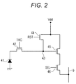
- Fig. 2 is a diagram illustrating an exemplary circuit configuration of a basic pixel.
- Fig. 3 is a diagram illustrating a first pixel circuit configuration in a pixel array unit of the solid-state imaging device.
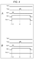
- Figs. 4A and 4B are timing charts illustrating examples of pixel driving.
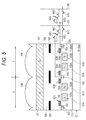
- Fig. 5 is a diagram illustrating a cross-sectional configuration of a pixel in a solid-state imaging device of a front side illumination type.
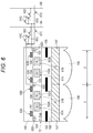
- Fig. 6 is a diagram illustrating a cross-sectional configuration of a pixel in a solid-state imaging device of a backside illumination type.
- Fig. 1 is a diagram illustrating a schematic configuration of a solid-state imaging device according to an embodiment of the present disclosure.
- Fig. 2 is a diagram illustrating an exemplary circuit configuration of a basic pixel.
- Fig. 3
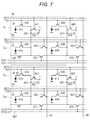
- FIG. 7 is a diagram illustrating a circuit configuration of a second pixel in the pixel array unit of the solid-state imaging device.
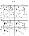
- Fig. 8 is a diagram illustrating a circuit configuration of a third pixel in the pixel array unit of the solid-state imaging device.
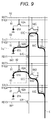
- Fig. 9 is an explanatory diagram for describing pixel operation in the third pixel circuit configuration.
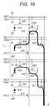
- Fig. 10 is an explanatory diagram for describing the pixel operation in the third pixel circuit configuration.
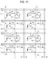
- Fig. 11 is a diagram illustrating a fourth pixel circuit configuration in the pixel array unit of the solid-state imaging device.
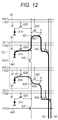
- Fig. 12 is an explanatory diagram for describing the pixel operation in the fourth pixel circuit configuration.
- FIG. 13 is an explanatory diagram for describing the pixel operation in the fourth pixel circuit configuration.
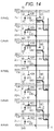
- Fig. 14 is a diagram for describing FD adding operation.
- Fig. 15 is a diagram illustrating a fifth pixel circuit configuration in the pixel array unit of the solid-state imaging device.
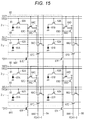
- Fig. 16 is a diagram illustrating a sixth pixel circuit configuration in the pixel array unit of the solid-state imaging device.
- Figs. 17A to 17C are diagrams illustrating exemplary substrate configurations of the solid-state imaging device.
- Fig. 18 is a block diagram illustrating an exemplary configuration of an imaging device as an electronic apparatus according to an embodiment of the present disclosure.
- Embodiments to carry out the present disclosure will be described. Note that a description will be provided in the following order.
- 1. Exemplary Schematic Configuration of Solid-State Imaging Device 2. Pixel Circuit Configuration According to First Embodiment (First Configuration Laterally Connecting FD Units) 3. Pixel Circuit Configuration According to Second Embodiment (Second Configuration Laterally Connecting FD Units) 4. Pixel Circuit Configuration According to Third Embodiment (First Configuration Vertically Connecting FD Units) 5. Pixel Circuit Configuration According to Fourth Embodiment (Second Configuration Vertically Connecting FD Units) 6. Pixel Circuit Configuration According to Fifth Embodiment (First Configuration Vertically and Laterally Connecting FD Units) 7. Pixel Circuit Configuration According to Sixth Embodiment (Configuration Having Reading Circuit Shared by Four Pixels) 8. Exemplary Application to Electronic Apparatus
- FIG. 1 is a diagram illustrating a schematic configuration of a solid-state imaging device according to an embodiment of the present disclosure.
- a solid-state imaging device 1 in Fig. 1 is includes, as a semiconductor, a semiconductor substrate 12 using silicon (Si), for example, on which a pixel array unit 3 where pixels 2 are arranged in a two-dimensional array and a peripheral circuit unit in a periphery are provided.
- the peripheral circuit unit includes, for example, a vertical drive circuit 4, a column signal processing circuit 5, a horizontal drive circuit 6, an output circuit 7, and a control circuit 8.
- the control circuit 8 receives data to command an input clock, an operation mode, and the like, and also outputs data such as internal information of the solid-state imaging device 1. More specifically, the control circuit 8 generates a clock signal and a control signal to be a basis of operation of the vertical drive circuit 4, column signal processing circuit 5, horizontal drive circuit 6, etc. based on a vertical synchronization signal, a horizontal synchronization signal, and a master clock. Further, the control circuit 8 outputs the generated clock signal and control signal to the vertical drive circuit 4, column signal processing circuit 5, horizontal drive circuit 6, and so on.
- the vertical drive circuit 4 is formed of, for example, a shift register, and selects a predetermined pixel drive wire 10 and supplies a pulse to the selected pixel drive wire 10 to drive the pixels 2, thereby driving the pixels 2 per row. More specifically, the vertical drive circuit 4 selectively scans, per row, respective pixels 2 of the pixel array unit 3 sequentially in the vertical direction, and the column signal processing circuit 5 is made to supply, via a vertical signal line 9, a pixel signal based on a signal electric charge generated at a photoelectric conversion unit of each pixel 2 in accordance with a received light amount.
- the column signal processing circuit 5 is disposed in each column of the pixel 2 and applies, per pixel column, signal processing such as noise removal to the signals output from the pixels 2 included in one row.
- the column signal processing circuit 5 applies the signal processing such as Correlated Double Sampling (CDS) to remove fixed pattern noise unique to the pixel, and AD conversion.
- CDS Correlated Double Sampling
- the horizontal drive circuit 6 is formed of, for example, a shift register and sequentially outputs horizontal scanning pulses, thereby sequentially selecting each of the column signal processing circuits 5 and causing each of the column signal processing circuits 5 to output a pixel signal to a horizontal signal line 11.
- the output circuit 7 applies signal processing to the signals sequentially supplied from the respective column signal processing circuits 5 via the horizontal signal line 11, and outputs the signals.
- the output circuit 7 may apply, for example, just buffering, and may apply black level adjustment, column variations correction, various kinds of digital signal processing, etc.
- An input and output terminal 13 exchanges signals with the outside.
- the solid-state imaging device 1 configured as described above is a CMOS image sensor called column A/D system, in which the column signal processing circuit 5 configured to execute the CDS processing and A/D conversion processing is arranged per pixel column.
- Fig. 2 is a diagram illustrating an exemplary circuit configuration of the basic pixel.
- the basic pixel includes a photodiode 41 as a photoelectric conversion unit, a transfer transistor 42, a floating diffusion (FD) unit 43, a reset transistor 44, an amplification transistor 45, and a selecting transistor 46.
- the photodiode 41 generates an electric charge (signal electric charge) in accordance with a received light amount and accumulates the electric charge.
- the photodiode 41 has an anode terminal grounded and a cathode terminal connected to the FD unit 43 via the transfer transistor 42.
- the transfer transistor 42 reads the electric charge generated at the photodiode 41 when a transfer signal TRG is turned on, and transfers the electric charge to the FD unit 43.
- the FD unit 43 holds the electric charge read from the photodiode 41.
- the reset transistor 44 resets electrical potential of the FD unit 43 when a reset signal RST is turned on and the electric charge accumulated in the FD unit 43 is discharged to a drain (constant voltage source Vdd).
- the amplification transistor 45 outputs a pixel signal corresponding to the electrical potential of the FD unit 43. More specifically, the amplification transistor 45 constitutes a source follower circuit together with a load MOS (not illustrated) as a constant current source connected via the vertical signal line 9, and a pixel signal indicating a level corresponding to the electric charge accumulated in the FD unit 43 is output from the amplification transistor 45 to the vertical signal line 9 via the selecting transistor 46.
- a load MOS not illustrated
- the selecting transistor 46 is turned on when a basic pixel is selected by a select signal SEL, and outputs the pixel signal of the basic pixel to the column signal processing circuit 5 via the vertical signal line 9.
- Respective control lines through which the transfer signal TRG, select signal SEL, and reset signal RST are transmitted correspond to the pixel drive wires 10 in Fig. 1.
- each pixel includes each of the transfer transistor 42, FD unit 43, reset transistor 44, amplification transistor 45, and selecting transistor 46 with respect to one photodiode 41.
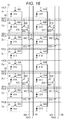
- FIG. 3 is a diagram illustrating a first pixel circuit configuration in a pixel array unit 3 of the solid-state imaging device 1.
- two of photodiodes 61 and transfer transistors 62 disposed adjacent vertically in the drawing share a reading circuit formed of an FD unit 63, a reset transistor 64, an amplification transistor 65, and a selecting transistor 66.
- Capacity of the FD unit 63 is set to an electric charge amount obtainable by one photodiode 61, for example.
- an FD connecting transistor 67 is disposed so as to connect respective FD units 63 laterally arrayed (row direction) in the drawing.
- the two photodiodes 61 laterally adjacent and surrounded by a dotted line in the drawing are included inside one pixel 2. More specifically, the pixel circuit of the solid-state imaging device 1 has a configuration in which the two photodiodes 61 are disposed in each pixel 2, and connection between the two FD units 63 holding the electric charges generated at the two photodiodes 61 is turned on/off by the FD connecting transistor 67.
- the two photodiodes 61 disposed inside one pixel and the transfer transistors are respectively differentiated as a photodiode 61A and transfer transistor 62A, and a photodiode 61B and a transfer transistor 62B.
- each one of the FD unit 63, reset transistor 64, amplification transistor 65, selecting transistor 66, and FD connecting transistor 67 respectively shared by the vertically adjacent two photodiodes 61A and the transfer transistors 62A are respectively defined as an FD unit 63C, a reset transistor 64C, an amplification transistor 65C, a selecting transistor 66C, and an FD connecting transistor 67C.
- each one of the FD unit 63, reset transistor 64, amplification transistor 65, selecting transistor 66, and FD connecting transistor 67 respectively shared by the vertically adjacent two photodiodes 61B and the transfer transistors 62B are defined respectively as an FD unit 63D, a reset transistor 64D, an amplification transistor 65D, a selecting transistor 66D, and an FD connecting transistor 67D.
- the photodiode 61, transfer transistor 62, FD unit 63, reset transistor 64, amplification transistor 65, and selecting transistor 66 have functions same as the functions of the above-described photodiode 41, transfer transistor 42, FD unit 43, reset transistor 44, amplification transistor 45, and selecting transistor 46 of the basic pixel.
- one transfer control line 81 is disposed per one pixel row along the row direction, and the transfer signal TRG is supplied to the transfer transistor 62 via the transfer control line 81.
- one reset control line 82 is disposed per two pixel rows along the row direction, and the reset signal RST is supplied to the reset transistor 64 via the reset control line 82.
- one select control line 83 is disposed per two pixel rows along the row direction, and the select signal SEL is supplied to the selecting transistor 66 via the select control line 83.
- two FD connection control lines 84X are disposed per pixel column along a column direction, and an FD connection signal FDX is supplied to the FD connecting transistor 67 via the FD connection control lines 84X.
- Two of the vertical signal lines 9 are also disposed, corresponding to the two photodiodes 61 in one pixel.
- Fig. 3 four pixels 2 11 to 2 14 located at four rows of a first column at an upper left corner of the pixel array unit 3 are illustrated, and the transfer signals TRG to be supplied to the transfer transistors 62 in the respective pixel rows inside the pixel array unit 3 are differentiated as transfer signals TRG1, TRG2, TRG3, TRG4, ..., corresponding to the array of the pixels 2.
- the reset transistors 64 and the selecting transistors 66 included inside the pixel array unit 3 one in each thereof is disposed with respect to the two photodiodes 61A adjacent vertically. Therefore, the reset signals RST and the select signals SEL respectively supplied to the respective reset transistors 64 and selecting transistors 66 are differentiated as reset signals RST1, RST3, (RST5)... and select signal SEL1, SEL3, (SEL5), and so on.
- the two FD connecting transistors 67 included inside the pixel array unit 3 are respectively disposed in the lateral direction in every pixel, and therefore, the FD connection signals FDX supplied to the respective FD connecting transistors 67 are differentiated as the FD connection signals FDX1-1, FDX1-2, (FDX2-1), (FDX2-2), and so on.
- the two of the vertical signal lines 9 are disposed per pixel, corresponding to the two reading circuits, and therefore, the vertical signal lines are differentiated as the vertical signal lines 9A and 9B.
- the FD connecting transistor 67C located between the two FD units 63C and 63D holding the electric charges generated by the two photodiodes 61A and 61B disposed inside one pixel is turned off by the FD connection signal FDX 1-1.
- the two FD units 63C and 63D are separated.
- the FD connecting transistor 67C located between the FD units 63C and 63D holding the electric charges generated by the two photodiodes 61A and 61B disposed inside one pixel is turned on by the FD connection signal FDX 1-1.
- the two FD units 63C and 63D are connected.
- the FD connecting transistor 67D can be connected to the FD unit 63C (not illustrated) in an adjacent pixel 2 22 in the case where the pixel 2 12 is used as the focus detecting pixel and the capacity for the photodiode 61B is variable.
- the two photodiodes 61A and 61B included inside one pixel are formed such that a light receiving area is divided into two portions, for example, in the vertical direction or in the lateral direction.
- a deviation may be caused on an image generated from the two photodiodes 61A and 61B because the two photodiodes 61A and 61B are formed in different positions inside one pixel.
- a phase deviation amount is calculated from the above deviation on the image, and a defocus amount is calculated. Then, an imaging capturing lens is adjusted (moved), thereby achieving automatic focus.
- Figs. 4A and 4B are timing charts illustrating examples of driving the pixel 2 12 out of the four pixels 2 11 to 2 14 illustrated in Fig. 3.
- Fig. 4A is the case where the pixel 2 12 is used as the image generating pixel
- Fig. 4B is the case where the pixel 2 12 is used as the focus detecting pixel. Note that the cases of other pixels 2 other than the pixel 2 12 are the same.
- the select signal SEL1 of the pixel 2 12 is set Hi, and the two selecting transistors 66C and 66D of the pixel 2 12 are turned on.
- the reset signal RST1 of the pixel 2 12 is initially set Hi for a predetermined period from time t2, and the two reset transistors 64C and 64D of the pixel 2 12 are turned on. By this, electrical potential of the two FD units 63C and 63D of the pixel 2 12 is reset.
- the transfer signal TRG2 of the pixel 2 12 is set Hi for a predetermined period from time t3, and the two transfer transistors 62A and 62B of the pixel 2 12 are turned on.
- the electric charges accumulated in the two photodiodes 61A and 61B of the pixel 2 12 are transferred to the corresponding FD units 63C and 63D respectively.
- the two selecting transistors 66C and 66D of the pixel 2 12 are turned on. Therefore, the electric charges transferred to the FD units 63C and 63D are converted to voltage signals and output to the vertical signal line 9A and vertical signal line 9B from the amplification transistors 65C and 65D via the selecting transistors 66C and 66D.
- the above operation is the same in the both of the cases where the pixel 2 12 is used as the image generating pixel and used as the focus detecting pixel.
- the FD connection signal FDX1-1 is different between the cases where the pixel 2 12 is used as the image generating pixel and used as the focus detecting pixel.
- the FD connection signal FDX1-1 is supplied to the FD connecting transistor 67C located between the two FD units 63C and 63D where the electric charges generated at the two photodiodes 61A and 61B disposed inside the pixel 2 12 .
- the FD connecting transistor 67C located between the two FD units 63C and 63D connected to the two photodiodes 61A and 61B inside the pixel 2 12 is turned on during the period in which the pixel 2 12 is selected, as illustrated in Fig. 4A.
- the FD connecting transistor 67C located between the two FD units 63C and 63D connected to the two photodiodes 61A and 61B inside the pixel 2 12 is turned off during the period in which the pixel 2 12 is selected, as illustrated in Fig. 4B.
- the pixel signal obtained at the photodiode 61A inside the pixel 2 12 and the pixel signal obtained at the photodiode 61B inside the pixel 2 12 are simultaneously output from the vertical signal line 9A and vertical signal line 9B.
- the pixel signal obtained at the photodiode 61A and the pixel signal obtained at the photodiode 61B inside the pixel 2 12 are processed as the same pixel signal because the pixel signals are combined by the FD connecting transistor 67C.
- the pixel signal obtained at the photodiode 61A and the pixel signal obtained at the photodiode 61B within the pixel 2 12 are processed as separate pixel signals (phase difference signals) because the pixel signals are separated by the FD connecting transistor 67C.
- the respective pixel signals at the divided two photodiodes 61A and 61B can be output simultaneously. Further, in the case where the pixel 2 is used as the image generating pixel, an image signal obtained by connecting the divided two photodiodes 61A and 61B can be output.
- the focus detecting pixel 2 does not become a defective pixel when an image is generated, different from the type of focus detecting pixel in which the pixel is partly shielded from the light.
- the two reading circuits are connected and used simultaneously. This enlarges an effective transistor size, thereby achieving to reduce noise of a source follower amplifier. Additionally, circuit noise can be reduced by using the separate column signal processing circuits 5 (A/D conversion units) via the two of vertical signal line 9A and vertical signal line 9B.
- the capacity of the FD unit 63 is optimally set for the electric charge amount obtainable by one photodiode 61. Therefore, in the both cases where the pixel 2 is used as the focus detecting pixel and as the image generating pixel, the capacity of the FD unit 63 is optimal. In other words, according to the first pixel circuit configuration of the present disclosure, both securing the dynamic range of the pixel signal and improving the S/N ratio can be achieved.
- control can be executed such that only one of the photodiodes 61 inside one pixel receives the light for the purpose of power consumption saving, in the same manner as the focus detecting pixel in which the pixel is partly shielded from the light.
- an unused FD unit 63 inside the same pixel is connected by turning on the FD connecting transistor 67C, and the capacity can be varied.
- the transfer control lines 81 of the transfer transistors 62A and 62B are separately provided, and the transfer signals TRG respectively supplied thereto are divided into, for example, TRG1A, TRG1B, TRG2A, TRG2B, and so on.
- Fig. 5 is a diagram illustrating a cross-sectional configuration of the pixel 2 in the solid-state imaging device 1.
- two n-type semiconductor regions 102A and 102B are formed in each pixel 2 relative to a p-type semiconductor region (P-Well) 101 formed on the n-type semiconductor substrate 12.
- the two n-type semiconductor regions 102A and 102B respectively constitute the photodiodes 61A and 61B by p-n junction with the p-type semiconductor region 101.
- An n-type semiconductor region 103 constituting the FD unit 63C or 63D is formed at a pixel boundary on an upper-side interfacial surface of the p-type semiconductor region 101.
- a gate electrode 104 of the transfer transistor 62A is formed of, for example, polysilicon on an upper surface of the semiconductor substrate 12 between the n-type semiconductor region 102A and the n-type semiconductor region 103.
- the gate electrode 104 of the transfer transistor 62B is formed of, for example, polysilicon on the upper surface of the semiconductor substrate 12 between the n-type semiconductor region 102B and the n-type semiconductor region 103.
- an inter-pixel shielding film 105 configured to avoid leakage of incident light from other adjacent pixels is formed of a metal film such as tungsten (W), aluminum (Al), or copper (Cu).
- a color filter 107 of red (R), green (G), or blue (B) is formed using, for example, nitride film (SiN), oxynitride film (SiON), oxide film (SiO2), and the like on the upper side of an insulation layer 106 having a flat upper surface, and an on-chip lens 108 is formed on the upper side of the color filter 107.
- the red (R), green (G), or blue (B) of the color filter 107 is arranged in a Bayer array, for example, but may also be arranged in accordance with other arraying methods.
- the color filter 107 is formed by performing spin-coating with photosensitive resin including pigments such as colorant and a dye.
- the on-chip lens 108 is formed of resin material, such as a styrene resin, an acrylic resin, a styrene-acrylic copolymer resin, or a siloxane-based resin.
- the reset transistors 64C and 64D, amplification transistors 65C and 65D, selecting transistors 66C and 66D, and FD connecting transistor 67C and 67D are formed in, for example, the inter-pixel area in the vertical direction, other than the cross-sectional portion illustrated in Fig. 5.
- the solid-state imaging device 1 can be formed of the solid-state imaging device of a front side illumination type in which the light enters from a front surface side of the semiconductor substrate 12 on which a pixel transistor is formed.
- the solid-state imaging device 1 may be formed of the solid-state imaging device of a backside illumination type in which the light enters from the back surface side opposite to the front surface side of the semiconductor substrate 12 on which the pixel transistor is formed.
- the semiconductor substrate 12 is a p-type substrate, and the n-type semiconductor regions 102A and 102B constituting the photodiodes 61A and 61B and the n-type semiconductor region 103 constituting the FD unit 63C or 63D are formed inside the p-type semiconductor substrate 12.
- the transfer transistors 62A and 62B are formed on the front surface side of the p-type semiconductor substrate 12 and covered with an insulation layer 109.
- the inter-pixel shielding film 105 and the insulation layer 106 are formed on the back surface side of the p-type semiconductor substrate 12, and the color filter 107 of red (R), green (G), or blue (B) and the on-chip lens 108 are formed on the upper side (on the lower side in Fig. 6) thereof.
- FIG. 7 is a diagram illustrating a second pixel circuit configuration in a pixel array unit 3 of a solid-state imaging device 1.
- an FD connection control line 84X configured to supply an FD connection signal FDX to an FD connecting transistor 67 is arranged along a column direction (vertical direction).
- an FD connection control line 84Y configured to supply an FD connection signal FDY to the FD connecting transistor 67 is arranged along a row direction (horizontal direction).
- two of the FD connection control lines 84Y are disposed and alternately connected to the adjacent FD connecting transistors 67 in order that the FD connecting transistors 67 laterally adjacent can be controlled differently.
- FIG. 8 is a diagram illustrating a third pixel circuit configuration in a pixel array unit 3 of a solid-state imaging device 1.
- an FD connecting transistor 67 is disposed so as to mutually connect respective FD units 63 laterally arrayed.
- the FD connecting transistor 67 is disposed so as to mutually connect the respective FD units 63 vertically arrayed as illustrated in Fig. 8.
- photodiodes 61A and 61B aligned in a vertical direction are included in one pixel 2.
- an FD unit 63C holding an electric charge generated at one photodiode 61A of a pixel 2 12 and an FD unit 63D holding an electric charge generated at the other photodiode 61B of the pixel 2 12 are connected via an FD connecting transistor 67E.
- An FD connection signal FDY1 is supplied to the FD connecting transistor 67E of the pixel 2 12 via an FD connection control line 84Y arranged along the row direction.
- an FD unit 63D where an electric charge generated at one photodiode 61A of a pixel 2 13 and an FD unit 63C (not illustrated) where an electric charge generated at the other photodiode 61B (not illustrated) of the pixel 2 13 are connected via an FD connecting transistor 67F of the pixel 2 13 .
- An FD connection signal FDY3 is supplied to the FD connecting transistor 67F of the pixel 2 13 via the FD connection control line 84Y.
- the FD connecting transistor 67E is turned on and the electric charge generated at the photodiode 61A and the electric charge generated at the photodiode 61B of the pixel 2 12 are simultaneously read as illustrated in Fig. 9.
- the electric charge generated at the photodiode 61A and the electric charge generated at the photodiode 61B of the pixel 2 12 are read by using both an amplification transistor 65C and an amplification transistor 65D, but can also be read only from one of the amplification transistor 65C and amplification transistor 65D.
- the electric charge generated at the photodiode 61A of the pixel 2 12 is output to a vertical signal line 9, passing through the FD unit 63C, the amplification transistor 65C, and a selecting transistor 66C as indicated by a thick solid line in Fig. 10.
- the electric charge generated at the photodiode 61B of the pixel 2 12 is output to the vertical signal line 9, passing through the FD unit 63D, the amplification transistor 65D and a selecting transistor 66D as indicated by a thick dotted line in Fig. 10.
- FIG. 11 is a diagram illustrating a pixel circuit configuration in which reading a signal electric charge of a photodiode 61A and reading a signal electric charge of a photodiode 61B are made to be performed simultaneously in the case where an FD connecting transistor 67 is disposed so as to mutually connect respective FD units 63 vertically arrayed.
- Fig. 11 is the diagram illustrating a fourth pixel circuit configuration in a pixel array unit 3 of a solid-state imaging device 1.
- two vertical signal lines 9C and 9D are disposed per pixel column.
- An amplification transistor 65C is connected to the vertical signal line 9C via a selecting transistor 66C, and an amplification transistor 65D is connected to the vertical signal line 9D via a selecting transistor 66D.
- a signal electric charge of the photodiode 61A and a signal electric charge of the photodiode 61B can be read simultaneously as illustrated in Fig. 12, and therefore high-speed reading can be achieved.
- pixel signals of a plurality of same color pixels adjacent in a vertical direction can be added at the FD units 63 and then output by simultaneously turning on transfer transistors 62 of the plurality of same color pixels adjacent in the vertical direction and simultaneously connecting the plurality of consecutive FD units 63.
- FIG. 15 is a diagram illustrating a fifth pixel circuit configuration in a pixel array unit 3 of a solid-state imaging device 1.
- the fifth pixel circuit configuration has a configuration in which FD connecting transistors 67E and 67F are further added to a first pixel circuit configuration illustrated in Fig. 3 such that respective FD units 63 can be further connected in the vertical direction.
- an FD unit 63C holding an electric charge generated at a photodiode 61A of a pixel 2 12 and an FD unit 63C holding an electric charge generated at the photodiode 61A of a pixel 2 13 are connected via the FD connecting transistor 67E.
- an FD unit 63D holding an electric charge generated at a photodiode 61B of a pixel 2 12 and an FD unit 63D holding an electric charge generated at the photodiode 61B of a pixel 213 are connected via the FD connecting transistor 67E.
- An FD connection signal FDY1 is supplied to each of FD connecting transistors 67E between the pixel 2 12 and the pixel 2 13 via an FD connection control line 84Y.
- the FD unit 63C holding an electric charge generated at a photodiode 61A and the FD unit 63D holding an electric charge generated at a photodiode 61B of a pixel 2 14 are also connected respectively to the FD unit 63C holding an electric charge generated at a photodiode 61A and the FD unit 63D holding an electric charge generated at a photodiode 61B of a pixel 2 15 not illustrated via the FD connecting transistors 67F.
- An FD connection signal FDY3 is supplied to each of the FD connecting transistors 67F between the pixel 2 14 and the pixel 2 15 via the FD connection control line 84Y.
- an FD connecting transistor 67C turns on/off connection between two FD units 63C and 63D that hold accumulated electric charges of the two photodiodes 61A and 61B inside one pixel. Therefore, the FD connecting transistor 67C is turned on/off depending on whether a pixel 2 is used as an image generating pixel or used as a focus detecting pixel.
- an FD connecting transistor 67D is turns on/off connection between the FD units 63 which hold accumulated electric charges of the pixels 2 adjacent in a row direction. Therefore, the FD connecting transistor 67D is turned on in the case of executing FD adding for pixel signals of a plurality of pixels 2 adjacent in the row direction or in the case of varying FD capacity.
- the FD connecting transistors 67E and 67F turn on/off connection between the FD units 63 which hold accumulated electric charges of the pixels 2 adjacent in a column direction. Therefore, the FD connecting transistors 67E and 67F are turned on in the case of executing FD adding for the pixel signals of the plurality of pixels 2 adjacent in the column direction or in the case of varying the FD capacity.
- a technology related to the present disclosure can also have a configuration in which the reading circuit can be shared by three or more adjacent pixels.
- Fig. 16 is a diagram illustrating a sixth pixel circuit configuration in a pixel array unit 3 of a solid-state imaging device 1.
- one reading circuit is shared by four pixels adjacent in a vertical direction.
- Other components are same as those in a first embodiment described above.
- a defective pixel is hardly generated in both of the cases of using a pixel 2 for focus detection and image generation because two photodiodes 61 are provided inside one pixel and electric charges respectively generated can be read by different reading circuits.
- pixel signals of divided two photodiodes 61A and 61B can be used as phase difference signals. Therefore, a circuit size increase can be minimized and also the focus detecting pixels can be arranged in high density.
- the FD unit 63 disposed corresponding to the photodiode 61 can be connected to the FD units 63 adjacent in the vertical direction, in the lateral direction or in both directions, capacity of the FD unit 63 can be varied.
- the capacity of the FD unit 63 is set optimal for an electric charge amount obtainable by one photodiode 61.
- the capacity of one FD unit 63 can be set smaller than the electric charge amount obtainable by one photodiode 61.
- freedom degree of the capacity of the FD unit 63 can be increased because of the configuration in which the FD unit 63 provided corresponding to the photodiode 61 can be connected to adjacent other FD units 63.
- the present technology can be used by using connection to reduce the capacity of the FD unit 63 to increase conversion efficiency, and when the received light amount is large, the present technology can be used by connecting the plurality of FD units 63 to increase the capacity and enlarge a dynamic range.
- reading may be executed by connecting the adjacent pixels 2 with the FD unit 63.
- an added signal can be obtained by executing FD adding on the pixel signals of the plurality of pixels.
- moire or the like may occur, but the moire or the like can be reduced by generating the added signal obtained by FD adding.
- FD adding of the pixel signals is more advantageous in aspects of power consumption and processing speed, comparing with analog addition or digital addition other than addition at the FD.
- the circuit configuration of the pixel 2 has been described to have the circuit configuration based on a rolling shutter system in which electric charges are sequentially generated and accumulated per pixel row by the photodiode 61.
- the circuit configuration may be of an all-pixel simultaneous reading system (global shutter method) whereby a second transfer transistor and a second electric charge holding unit are added between the transfer transistor 62 and the FD unit 63, exposure operation is executed at all pixels inside the pixel array unit 3, electric charges are temporarily held at the second electric charge holding unit until start of reading, and reading is executed per row.
- the solid-state imaging device 1 in Fig. 1 includes one semiconductor substrate 12 on which a pixel area 121 on which the plurality of pixels 2 is arrayed, a control circuit 122 configured to control the pixel 2, and a logic circuit 123 including a signal processing circuit for a pixel signal are formed.
- the solid-state imaging device 1 may have a configuration in which a first semiconductor substrate 131 formed with the pixel area 121 and the control circuit 122 and a second semiconductor substrate 132 formed with the logic circuit 123 are laminated.
- the first semiconductor substrate 131 and the second semiconductor substrate 132 are electrically connected by, for example, a through via or Cu-Cu metal binding.
- the solid-state imaging device 1 may have a configuration in which a first semiconductor substrate 141 formed with only the pixel area 121 and a second semiconductor substrate 142 formed with the control circuit 122 and the logic circuit 123 laminated.
- the first semiconductor substrate 141 and the second semiconductor substrate 142 are electrically connected by, for example, the through via or Cu-Cu metal binding.
- the solid-state imaging device may be formed as one chip, and also may have a module-like form having an imaging function in which an imaging unit and a signal processing unit or an optical system are integrally packaged.
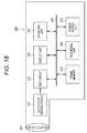
- Fig. 18 is a block diagram illustrating an exemplary configuration of the imaging device as the electronic apparatus according to an embodiment of the present disclosure.
- An imaging device 200 in Fig. 18 includes an optical unit 201 formed of, for example, a group of lenses, a solid-state imaging device (imaging device) 202 in which the solid-state imaging device 1 in Fig. 1 is adopted, and a Digital Signal Processor (DSP) circuit 203 which is a camera signal processing circuit. Further, the imaging device 200 also includes a frame memory 204, a display unit 205, a recording unit 206, an operating unit 207, and a power source unit 208. The DSP circuit 203, frame memory 204, display unit 205, recording unit 206, operating unit 207, and power source unit 208 are mutually connected via a bus line 209.
- DSP Digital Signal Processor
- the optical unit 201 takes in incident light (image light) from an object and forms an image on an imaging area of the solid-state imaging device 202.
- the solid-state imaging device 202 converts, per pixel, a light amount of the incident light formed on the imaging area by the optical unit 201 to an electric signal, and outputs the electric signal as a pixel signal.
- the solid-state imaging device 202 the solid-state imaging device 1 in Fig. 1, more specifically, the solid-state imaging device having a downsized circuit size can be used without generating any defective pixel by turning on/off connection between the two FD units 63 when the pixel 2 is used for focus detection and image generation.
- the display unit 205 may be formed of, for example, a panel type display unit such as a liquid crystal panel and an organic electro luminescence (EL) panel, and configured to display a moving image or a still image imaged by the solid-state imaging device 202.
- the recording unit 206 records the moving image or the still image imaged by the solid-state imaging device 202 in a recoding medium such as a hard disk and a semiconductor memory.
- the operating unit 207 issues an operational command relative to various kinds of functions included in the imaging device 200 in accordance with a user's operation.
- the power source unit 208 suitably supplies following supply targets with various kinds of power to be operation power sources of the DSP circuit 203, frame memory 204, display unit 205, recording unit 206, and operating unit 207.
- the focus detection pixels can be arranged in high density, and the image can be captured without generating a defective pixel. Therefore, quality of the captured image can be improved in the imaging device 200 such as a video camera, a digital still camera, and further a camera module for a mobile apparatus like a cell phone.
- the solid-state imaging device in which a first conductivity type is the p-type, a second conductivity type is the n-type, and an electron is a signal electric charge.
- the technology of the present disclosure is applicable to a solid-state imaging device in which a positive hole is used as the signal electric charge.
- the above-described respective semiconductor regions may be formed of semiconductor regions having reverse conductivity types in which the first conductivity type is the n-type and the second conductivity type is the p-type.
- the technology according to an embodiment of the present disclosure is applicable not only to the solid-state imaging device configured to detect and capture distribution of an incident light amount of visible light as an image but also to a solid-state imaging device configured to detect and capture, as an image, the distribution of the incident light amount of, such as an infrared ray, an X-ray or a particle, and in a broad sense, to all of the solid-state imaging devices (physical amount distribution detecting devices) such as a fingerprint detection sensor configured to detect and capture distribution of other physical amounts such as pressure and capacitance as an image.
- the solid-state imaging devices physical amount distribution detecting devices
- a fingerprint detection sensor configured to detect and capture distribution of other physical amounts such as pressure and capacitance as an image.
- a solid-state imaging device in which each of a plurality of pixels two-dimensionally arranged in a matrix shape includes a first photoelectric conversion unit and a second photoelectric conversion unit both configured to photoelectrically convert light entering via one micro lens, including: a first reading circuit configured to read an electric charge generated at the first photoelectric conversion unit; a second reading circuit configured to read an electric charge generated at the second photoelectric conversion unit; and a transistor configured to connect a first electric charge holding unit included in the first reading circuit to a second electric charge holding unit included in the second reading circuit.
- a driving method for a solid-state imaging device in which each of a plurality of pixels two-dimensionally arranged in a matrix shape includes a first photoelectric conversion unit and a second photoelectric conversion unit both configured to photoelectrically convert light entering via one micro lens
- the solid-state imaging device including: a first reading circuit configured to read an electric charge generated at the first photoelectric conversion unit; a second reading circuit configured to read an electric charge generated at the second photoelectric conversion unit; and a transistor configured to connect a first electric charge holding unit included in the first reading circuit to a second electric charge holding unit included in the second reading circuit, wherein the transistor connects the first electric charge holding unit to the second electric charge holding unit in the case of using the pixel as an image generating pixel, and the transistor separates the first electric charge holding unit from the second electric charge holding unit in the case of using the pixel as a focus detecting pixel.
- An electronic apparatus including a solid-state imaging device in which each of a plurality of pixels two-dimensionally arranged in a matrix shape includes a first photoelectric conversion unit and a second photoelectric conversion unit both configured to photoelectrically convert light entering via one micro lens, the solid-state imaging device including: a first reading circuit configured to read an electric charge generated at the first photoelectric conversion unit; a second reading circuit configured to read an electric charge generated at the second photoelectric conversion unit; and a transistor configured to connect a first electric charge holding unit included in the first reading circuit to a second electric charge holding unit included in the second reading circuit.
- Solid-state imaging device 1 Solid-state imaging device 2 Pixel 3 Pixel array unit 12 Semiconductor substrate 61 Photodiode 62 Transfer transistor 63 FD unit 64 Reset transistor 65 Amplification transistor 66 Selecting transistor 67 FD connecting transistor 84X, 84Y FD connection control line 131 First semiconductor substrate 132 Second semiconductor substrate 141 First semiconductor substrate 142 Second semiconductor substrate 200 Imaging device 202 Solid-state imaging device
Landscapes
- Engineering & Computer Science (AREA)
- Physics & Mathematics (AREA)
- Power Engineering (AREA)
- General Physics & Mathematics (AREA)
- Electromagnetism (AREA)
- Condensed Matter Physics & Semiconductors (AREA)
- Computer Hardware Design (AREA)
- Microelectronics & Electronic Packaging (AREA)
- Signal Processing (AREA)
- Multimedia (AREA)
- Solid State Image Pick-Up Elements (AREA)
- Transforming Light Signals Into Electric Signals (AREA)
- Automatic Focus Adjustment (AREA)
Abstract
Description
This application claims the benefit of Japanese Priority Patent Application JP 2014-053667 filed on March 17, 2014, the entire contents of which are incorporated herein by reference.
1. Exemplary Schematic Configuration of Solid-State Imaging Device
2. Pixel Circuit Configuration According to First Embodiment (First Configuration Laterally Connecting FD Units)
3. Pixel Circuit Configuration According to Second Embodiment (Second Configuration Laterally Connecting FD Units)
4. Pixel Circuit Configuration According to Third Embodiment (First Configuration Vertically Connecting FD Units)
5. Pixel Circuit Configuration According to Fourth Embodiment (Second Configuration Vertically Connecting FD Units)
6. Pixel Circuit Configuration According to Fifth Embodiment (First Configuration Vertically and Laterally Connecting FD Units)
7. Pixel Circuit Configuration According to Sixth Embodiment (Configuration Having Reading Circuit Shared by Four Pixels)
8. Exemplary Application to Electronic Apparatus
Fig. 1 is a diagram illustrating a schematic configuration of a solid-state imaging device according to an embodiment of the present disclosure.
Next, a pixel circuit inside the
In contrast, Fig. 3 is a diagram illustrating a first pixel circuit configuration in a
Figs. 4A and 4B are timing charts illustrating examples of driving the
Fig. 5 is a diagram illustrating a cross-sectional configuration of the
Fig. 7 is a diagram illustrating a second pixel circuit configuration in a
Fig. 8 is a diagram illustrating a third pixel circuit configuration in a
Now, Fig. 11 is a diagram illustrating a pixel circuit configuration in which reading a signal electric charge of a
Fig. 15 is a diagram illustrating a fifth pixel circuit configuration in a
In first to fifth embodiments described above, a description has been given for examples in which a reading circuit formed of an FD unit 63, a reset transistor 64, an amplification transistor 65, and a selecting transistor 66 is shared by adjacent two pixels.
As illustrated in Fig. 17A, the solid-
Application of the technology of the present disclosure is not limited to the solid-state imaging device. More specifically, the technology of the present disclosure is applicable to all of electronic apparatuses using a solid-state imaging device at an image capturing unit (photoelectric conversion unit), for example, imaging devices such as a digital still camera and a video camera, a portable terminal device having an imaging function, a copier using a solid-state imaging device at an image reading unit, and so on. The solid-state imaging device may be formed as one chip, and also may have a module-like form having an imaging function in which an imaging unit and a signal processing unit or an optical system are integrally packaged.
(1)
A solid-state imaging device in which each of a plurality of pixels two-dimensionally arranged in a matrix shape includes a first photoelectric conversion unit and a second photoelectric conversion unit both configured to photoelectrically convert light entering via one micro lens, including:
a first reading circuit configured to read an electric charge generated at the first photoelectric conversion unit;
a second reading circuit configured to read an electric charge generated at the second photoelectric conversion unit; and
a transistor configured to connect a first electric charge holding unit included in the first reading circuit to a second electric charge holding unit included in the second reading circuit.
(2)
The solid-state imaging device according to above (1), wherein the transistor connects the first electric charge holding unit to the second electric charge holding unit in the case of using the pixel as an image generating pixel, and the transistor separates the first electric charge holding unit from the second electric charge holding unit in the case of using the pixel as a focus detecting pixel.
(3)
The solid-state imaging device according to above (1) or (2), wherein in the case where the pixel is used as the focus detecting pixel, reading the electric charge of the first photoelectric conversion unit by the first reading circuit and reading the electric charge of the second photoelectric conversion unit by the second reading circuit are simultaneously executed.
(4)
The solid-state imaging device according to any one of above (1) to (3), wherein each of the first reading circuit and the second reading circuit is shared by photoelectric conversion units of one or more of other adjacent pixels.
(5)
The solid-state imaging device according to above (4), wherein each of the first reading circuit and the second reading circuit is shared by photoelectric conversion units of a plurality of other adjacent pixels.
(6)
The solid-state imaging device according to any one of above (1) to (5), wherein a control line configured to control the transistor is disposed along a column direction.
(7)
The solid-state imaging device according to any one of above (1) to (5), wherein a control line configured to control the transistor is disposed along a row direction.
(8)
The solid-state imaging device according to any one of above (1) to (7), wherein a backside illumination type is adopted.
(9)
The solid-state imaging device according to any one of above (1) to (7), wherein a front side illumination type is adopted.
(10)
The solid-state imaging device according to any one of above (1) to (9), including a circuit configuration in which the pixel executes exposure operation at the plurality of pixels simultaneously, and reading is executed per row.
(11)
The solid-state imaging device according to any one of above (1) to (10), having a configuration in which a first semiconductor substrate at least formed with a pixel area on which the plurality of pixels is arrayed and a second semiconductor substrate at least formed with a logic circuit configured to process a pixel signal output from the pixel are laminated.
(12)
A driving method for a solid-state imaging device in which each of a plurality of pixels two-dimensionally arranged in a matrix shape includes a first photoelectric conversion unit and a second photoelectric conversion unit both configured to photoelectrically convert light entering via one micro lens, the solid-state imaging device including:
a first reading circuit configured to read an electric charge generated at the first photoelectric conversion unit;
a second reading circuit configured to read an electric charge generated at the second photoelectric conversion unit; and
a transistor configured to connect a first electric charge holding unit included in the first reading circuit to a second electric charge holding unit included in the second reading circuit,
wherein the transistor connects the first electric charge holding unit to the second electric charge holding unit in the case of using the pixel as an image generating pixel, and the transistor separates the first electric charge holding unit from the second electric charge holding unit in the case of using the pixel as a focus detecting pixel.
(13)
An electronic apparatus including a solid-state imaging device in which each of a plurality of pixels two-dimensionally arranged in a matrix shape includes a first photoelectric conversion unit and a second photoelectric conversion unit both configured to photoelectrically convert light entering via one micro lens, the solid-state imaging device including:
a first reading circuit configured to read an electric charge generated at the first photoelectric conversion unit;
a second reading circuit configured to read an electric charge generated at the second photoelectric conversion unit; and
a transistor configured to connect a first electric charge holding unit included in the first reading circuit to a second electric charge holding unit included in the second reading circuit.
2 Pixel
3 Pixel array unit
12 Semiconductor substrate
61 Photodiode
62 Transfer transistor
63 FD unit
64 Reset transistor
65 Amplification transistor
66 Selecting transistor
67 FD connecting transistor
84X, 84Y FD connection control line
131 First semiconductor substrate
132 Second semiconductor substrate
141 First semiconductor substrate
142 Second semiconductor substrate
200 Imaging device
202 Solid-state imaging device
Claims (13)
- A solid-state imaging device in which each of a plurality of pixels two-dimensionally arranged in a matrix shape includes a first photoelectric conversion unit and a second photoelectric conversion unit both configured to photoelectrically convert light entering via one micro lens, comprising:
a first reading circuit configured to read an electric charge generated at the first photoelectric conversion unit;
a second reading circuit configured to read an electric charge generated at the second photoelectric conversion unit; and
a transistor configured to connect a first electric charge holding unit included in the first reading circuit to a second electric charge holding unit included in the second reading circuit. - The solid-state imaging device according to claim 1, wherein the transistor connects the first electric charge holding unit to the second electric charge holding unit in the case of using the pixel as an image generating pixel, and the transistor separates the first electric charge holding unit from the second electric charge holding unit in the case of using the pixel as a focus detecting pixel.
- The solid-state imaging device according to claim 1, wherein in the case where the pixel is used as the focus detecting pixel, reading the electric charge of the first photoelectric conversion unit by the first reading circuit and reading the electric charge of the second photoelectric conversion unit by the second reading circuit are simultaneously executed.
- The solid-state imaging device according to claim 1, wherein each of the first reading circuit and the second reading circuit is shared by photoelectric conversion units of one or more other adjacent pixels.
- The solid-state imaging device according to claim 4, wherein each of the first reading circuit and the second reading circuit is shared by photoelectric conversion units of a plurality of other adjacent pixels.
- The solid-state imaging device according to claim 1, wherein a control line configured to control the transistor is disposed along a column direction.
- The solid-state imaging device according to claim 1, wherein a control line configured to control the transistor is disposed along a row direction.
- The solid-state imaging device according to claim 1, wherein a backside illumination type is adopted.
- The solid-state imaging device according to claim 1, wherein a front side illumination type is adopted.
- The solid-state imaging device according to claim 1, having a circuit configuration in which the pixel executes exposure operation at the plurality of pixels simultaneously, and reading is executed per row.
- The solid-state imaging device according to claim 1, having a configuration in which a first semiconductor substrate at least formed with a pixel area on which the plurality of pixels is arrayed and a second semiconductor substrate at least formed with a logic circuit configured to process a pixel signal output from the pixel are laminated.
- A driving method for a solid-state imaging device in which each of a plurality of pixels two-dimensionally arranged in a matrix shape includes a first photoelectric conversion unit and a second photoelectric conversion unit both configured to photoelectrically convert light entering via one micro lens, the solid-state imaging device including:
a first reading circuit configured to read an electric charge generated at the first photoelectric conversion unit;
a second reading circuit configured to read an electric charge generated at the second photoelectric conversion unit; and
a transistor configured to connect a first electric charge holding unit included in the first reading circuit to a second electric charge holding unit included in the second reading circuit,
wherein the transistor connects the first electric charge holding unit to the second electric charge holding unit in the case of using the pixel as an image generating pixel, and the transistor separates the first electric charge holding unit from the second electric charge holding unit in the case of using the pixel as a focus detecting pixel. - An electronic apparatus comprising a solid-state imaging device in which each of a plurality of pixels two-dimensionally arranged in a matrix shape includes a first photoelectric conversion unit and a second photoelectric conversion unit both configured to photoelectrically convert light entering via one micro lens, the solid-state imaging device including:
a first reading circuit configured to read an electric charge generated at the first photoelectric conversion unit;
a second reading circuit configured to read an electric charge generated at the second photoelectric conversion unit; and
a transistor configured to connect a first electric charge holding unit included in the first reading circuit to a second electric charge holding unit included in the second reading circuit.
Priority Applications (4)
| Application Number | Priority Date | Filing Date | Title |
|---|---|---|---|
| KR1020157030922A KR102369398B1 (en) | 2014-03-17 | 2015-03-04 | Solid-state imaging device, driving method therefor, and electronic apparatus |
| KR1020227005598A KR102542664B1 (en) | 2014-03-17 | 2015-03-04 | Solid-state imaging device, driving method therefor, and electronic apparatus |
| CN201580000727.2A CN105210363B (en) | 2014-03-17 | 2015-03-04 | The driving method and electronic equipment of solid photographic device, solid photographic device |
| US14/889,947 US10403672B2 (en) | 2014-03-17 | 2015-03-04 | Solid-state imaging device with pixels having first and second photoelectric conversion units, driving method therefor, and electronic apparatus |
Applications Claiming Priority (2)
| Application Number | Priority Date | Filing Date | Title |
|---|---|---|---|
| JP2014-053667 | 2014-03-17 | ||
| JP2014053667A JP6075646B2 (en) | 2014-03-17 | 2014-03-17 | Solid-state imaging device, driving method thereof, and electronic apparatus |
Publications (1)
| Publication Number | Publication Date |
|---|---|
| WO2015141161A1 true WO2015141161A1 (en) | 2015-09-24 |
Family
ID=52774437
Family Applications (1)
| Application Number | Title | Priority Date | Filing Date |
|---|---|---|---|
| PCT/JP2015/001142 WO2015141161A1 (en) | 2014-03-17 | 2015-03-04 | Solid-state imaging device, driving method therefor, and electronic apparatus |
Country Status (6)
| Country | Link |
|---|---|
| US (1) | US10403672B2 (en) |
| JP (1) | JP6075646B2 (en) |
| KR (2) | KR102542664B1 (en) |
| CN (1) | CN105210363B (en) |
| TW (1) | TWI653892B (en) |
| WO (1) | WO2015141161A1 (en) |
Cited By (4)
| Publication number | Priority date | Publication date | Assignee | Title |
|---|---|---|---|---|
| WO2017101864A1 (en) * | 2015-12-18 | 2017-06-22 | 广东欧珀移动通信有限公司 | Image sensor, control method, and electronic device |
| US10715755B2 (en) | 2016-03-31 | 2020-07-14 | Sony Corporation | Solid-state image sensor and imaging device |
| FR3129526A1 (en) * | 2021-11-25 | 2023-05-26 | Stmicroelectronics (Crolles 2) Sas | Image sensor |
| US12009381B2 (en) | 2019-05-31 | 2024-06-11 | Sony Semiconductor Solutions Corporation | Solid-state imaging device |
Families Citing this family (29)
| Publication number | Priority date | Publication date | Assignee | Title |
|---|---|---|---|---|
| JP6588702B2 (en) * | 2015-01-05 | 2019-10-09 | キヤノン株式会社 | Imaging apparatus, control method therefor, program, and storage medium |
| JP5897752B1 (en) * | 2015-05-14 | 2016-03-30 | ブリルニクスジャパン株式会社 | Solid-state imaging device, driving method thereof, and electronic apparatus |
| KR20170019581A (en) * | 2015-08-12 | 2017-02-22 | 삼성전자주식회사 | Fingerprint sensor, electronic device having the same, and method of operating fingerprint sensor |
| JP6746301B2 (en) | 2015-11-30 | 2020-08-26 | キヤノン株式会社 | Imaging device driving method, imaging device, and imaging system |
| JP6663209B2 (en) * | 2015-11-30 | 2020-03-11 | キヤノン株式会社 | Imaging device, imaging system, and driving method of imaging device |
| JP6600246B2 (en) * | 2015-12-17 | 2019-10-30 | キヤノン株式会社 | Imaging apparatus and camera |
| JP2017142356A (en) | 2016-02-10 | 2017-08-17 | ソニー株式会社 | Image pickup apparatus, and control method for the same |
| JP7075881B2 (en) * | 2016-02-29 | 2022-05-26 | 株式会社ニコン | Image sensor and image sensor |
| US9936150B2 (en) * | 2016-03-17 | 2018-04-03 | Semiconductor Components Industries, Llc | Image sensors with a rolling shutter scanning mode and high dynamic range |
| CN113542633B (en) * | 2016-05-24 | 2024-09-17 | 索尼公司 | Image forming apparatus and image forming apparatus |
| JP6765859B2 (en) | 2016-05-31 | 2020-10-07 | キヤノン株式会社 | Imaging device and its control method |
| WO2017209221A1 (en) * | 2016-05-31 | 2017-12-07 | ソニーセミコンダクタソリューションズ株式会社 | Image capturing device, image capturing method, camera module, and electronic device |
| JP6688165B2 (en) * | 2016-06-10 | 2020-04-28 | キヤノン株式会社 | Imaging device and imaging system |
| JP6778595B2 (en) * | 2016-08-17 | 2020-11-04 | ルネサスエレクトロニクス株式会社 | Image sensor |
| US10038863B2 (en) * | 2016-08-17 | 2018-07-31 | Renesas Electronics Corporation | Image sensing device |
| JP6804140B2 (en) * | 2016-09-02 | 2020-12-23 | 東芝情報システム株式会社 | Solid-state image sensor |
| JP6667431B2 (en) * | 2016-12-27 | 2020-03-18 | キヤノン株式会社 | Imaging device, imaging system |
| JP6769349B2 (en) * | 2017-03-03 | 2020-10-14 | 株式会社リコー | Solid-state image sensor and image sensor |
| WO2018181463A1 (en) * | 2017-03-31 | 2018-10-04 | ブリルニクスジャパン株式会社 | Solid-state imaging apparatus, method for driving solid-state imaging apparatus, and electronic device |
| JP2019050522A (en) | 2017-09-11 | 2019-03-28 | キヤノン株式会社 | Imaging device |
| CN115767293B (en) | 2017-11-22 | 2023-07-14 | 索尼半导体解决方案公司 | Light detection device and image pickup device |
| JP7013973B2 (en) * | 2018-03-19 | 2022-02-01 | 株式会社リコー | Solid-state image sensor and image sensor |
| JP7176559B2 (en) * | 2018-03-30 | 2022-11-22 | 株式会社ニコン | Imaging element and imaging device |
| JP7111810B2 (en) * | 2018-05-29 | 2022-08-02 | オリンパス株式会社 | Solid-state imaging device and imaging system |
| US10890482B2 (en) | 2019-01-18 | 2021-01-12 | Himax Imaging Limited | Pixel circuit for generating an output signal in response to incident radiation |
| US11381768B2 (en) * | 2019-05-07 | 2022-07-05 | Samsung Electronics Co., Ltd. | Image sensor with pixels including photodiodes sharing floating diffusion region |
| US11653110B2 (en) | 2020-09-18 | 2023-05-16 | Samsung Electronics Co., Ltd. | Image sensor |
| US20220116557A1 (en) * | 2020-10-08 | 2022-04-14 | Samsung Electronics Co., Ltd. | Pixel array and image sensor including the same |
| WO2024106196A1 (en) * | 2022-11-16 | 2024-05-23 | ソニーセミコンダクタソリューションズ株式会社 | Solid-state imaging device and electronic apparatus |
Citations (2)
| Publication number | Priority date | Publication date | Assignee | Title |
|---|---|---|---|---|
| JP2007243744A (en) * | 2006-03-10 | 2007-09-20 | Nikon Corp | Solid-state imaging device and electronic camera using the same |
| US20140061436A1 (en) * | 2012-09-04 | 2014-03-06 | Canon Kabushiki Kaisha | Solid state imaging device |
Family Cites Families (22)
| Publication number | Priority date | Publication date | Assignee | Title |
|---|---|---|---|---|
| JP3774597B2 (en) | 1999-09-13 | 2006-05-17 | キヤノン株式会社 | Imaging device |
| JP2001250931A (en) * | 2000-03-07 | 2001-09-14 | Canon Inc | Solid-state image sensor and image sensing system using the same |
| JP2002043381A (en) * | 2000-07-19 | 2002-02-08 | Tokyo Electron Ltd | Water temperature controller |
| US6521881B2 (en) * | 2001-04-16 | 2003-02-18 | Kingpak Technology Inc. | Stacked structure of an image sensor and method for manufacturing the same |
| KR20050095792A (en) * | 2003-02-20 | 2005-10-04 | 닛뽄 세이꼬 가부시기가이샤 | Electric-powered power steering apparatus |
| CN101213829A (en) | 2005-06-01 | 2008-07-02 | 伊斯曼柯达公司 | CMOS image sensor pixel with selectable binning |
| US7705900B2 (en) * | 2005-06-01 | 2010-04-27 | Eastman Kodak Company | CMOS image sensor pixel with selectable binning and conversion gain |
| US7613157B2 (en) * | 2005-08-30 | 2009-11-03 | Interdigital Technology Corporation | Wireless communication method and apparatus for processing enhanced uplink scheduling grants |
| AU2008275873B2 (en) * | 2007-07-19 | 2013-06-06 | Disney Enterprises, Inc. | Methods and apparatus for multiple texture map storage and filtering |
| KR20090090776A (en) * | 2008-02-22 | 2009-08-26 | 삼성전자주식회사 | Image sensor and method for manufacturing the same |
| US7777171B2 (en) * | 2008-08-26 | 2010-08-17 | Eastman Kodak Company | In-pixel summing of charge generated by two or more pixels having two reset transistors connected in series |
| US8913166B2 (en) * | 2009-01-21 | 2014-12-16 | Canon Kabushiki Kaisha | Solid-state imaging apparatus |
| JP5359465B2 (en) * | 2009-03-31 | 2013-12-04 | ソニー株式会社 | Solid-state imaging device, signal processing method for solid-state imaging device, and imaging device |
| JP5511541B2 (en) * | 2010-06-24 | 2014-06-04 | キヤノン株式会社 | Solid-state imaging device and driving method of solid-state imaging device |
| US20130018215A1 (en) * | 2011-01-18 | 2013-01-17 | Merit Medical Systems, Inc. | Esophageal stent and methods for use of same |
| JP5839807B2 (en) * | 2011-02-09 | 2016-01-06 | キヤノン株式会社 | Method for manufacturing solid-state imaging device |
| JP5885403B2 (en) * | 2011-06-08 | 2016-03-15 | キヤノン株式会社 | Imaging device |
| JP6172888B2 (en) * | 2012-01-18 | 2017-08-02 | キヤノン株式会社 | Imaging apparatus and imaging system |
| JP2013157883A (en) | 2012-01-31 | 2013-08-15 | Sony Corp | Solid-state imaging device and camera system |
| JP2013172210A (en) * | 2012-02-17 | 2013-09-02 | Canon Inc | Imaging device |
| US9554115B2 (en) * | 2012-02-27 | 2017-01-24 | Semiconductor Components Industries, Llc | Imaging pixels with depth sensing capabilities |
| JP6164867B2 (en) * | 2013-02-21 | 2017-07-19 | キヤノン株式会社 | Solid-state imaging device, control method thereof, and control program |
-
2014
- 2014-03-17 JP JP2014053667A patent/JP6075646B2/en active Active
-
2015
- 2015-01-30 TW TW104103322A patent/TWI653892B/en active
- 2015-03-04 KR KR1020227005598A patent/KR102542664B1/en active IP Right Grant
- 2015-03-04 CN CN201580000727.2A patent/CN105210363B/en active Active
- 2015-03-04 US US14/889,947 patent/US10403672B2/en active Active
- 2015-03-04 KR KR1020157030922A patent/KR102369398B1/en active IP Right Grant
- 2015-03-04 WO PCT/JP2015/001142 patent/WO2015141161A1/en active Application Filing
Patent Citations (2)
| Publication number | Priority date | Publication date | Assignee | Title |
|---|---|---|---|---|
| JP2007243744A (en) * | 2006-03-10 | 2007-09-20 | Nikon Corp | Solid-state imaging device and electronic camera using the same |
| US20140061436A1 (en) * | 2012-09-04 | 2014-03-06 | Canon Kabushiki Kaisha | Solid state imaging device |
Cited By (6)
| Publication number | Priority date | Publication date | Assignee | Title |
|---|---|---|---|---|
| WO2017101864A1 (en) * | 2015-12-18 | 2017-06-22 | 广东欧珀移动通信有限公司 | Image sensor, control method, and electronic device |
| US10313612B2 (en) | 2015-12-18 | 2019-06-04 | Guangdong Oppo Mobile Telecommunications Corp., Ltd. | Image sensor, control method, and electronic device |
| US10715755B2 (en) | 2016-03-31 | 2020-07-14 | Sony Corporation | Solid-state image sensor and imaging device |
| US12009381B2 (en) | 2019-05-31 | 2024-06-11 | Sony Semiconductor Solutions Corporation | Solid-state imaging device |
| FR3129526A1 (en) * | 2021-11-25 | 2023-05-26 | Stmicroelectronics (Crolles 2) Sas | Image sensor |
| US12075178B2 (en) | 2021-11-25 | 2024-08-27 | Stmicroelectronics (Crolles 2) Sas | Image sensor |
Also Published As
| Publication number | Publication date |
|---|---|
| CN105210363A (en) | 2015-12-30 |
| KR20220025945A (en) | 2022-03-03 |
| US10403672B2 (en) | 2019-09-03 |
| US20160141326A1 (en) | 2016-05-19 |
| CN105210363B (en) | 2019-08-09 |
| TW201537983A (en) | 2015-10-01 |
| KR102369398B1 (en) | 2022-03-04 |
| KR102542664B1 (en) | 2023-06-14 |
| KR20160132342A (en) | 2016-11-18 |
| JP2015177429A (en) | 2015-10-05 |
| TWI653892B (en) | 2019-03-11 |
| JP6075646B2 (en) | 2017-02-08 |
Similar Documents
| Publication | Publication Date | Title |
|---|---|---|
| US10403672B2 (en) | Solid-state imaging device with pixels having first and second photoelectric conversion units, driving method therefor, and electronic apparatus | |
| US10651213B2 (en) | Solid-state image pickup device and method of driving the same | |
| US11902678B2 (en) | Solid-state imaging device, method of driving the same, and electronic apparatus | |
| US10021321B2 (en) | Imaging device and imaging system | |
| CN105308748B (en) | Solid-state imaging device and electronic apparatus | |
| US20190098239A1 (en) | Solid-state imaging device, method for driving the same, and electronic device | |
| US10594961B2 (en) | Generation of pixel signal with a high dynamic range and generation of phase difference information | |
| US9591244B2 (en) | Solid-state imaging device having plural hybrid pixels with dual storing function | |
| US10666914B2 (en) | Solid state imaging device and electronic apparatus in which the area of the photodiode may be expanded | |
| US8355068B2 (en) | Solid-state image sensing device, analog-digital conversion method of solid-state image sensing device, and electronic apparatus | |
| US10840288B2 (en) | Imaging device, imaging apparatus, and image input device | |
| WO2019069532A1 (en) | Solid-state imaging element and solid-state imaging device | |
| US9338374B2 (en) | Solid-state image sensor, method for driving solid-state image sensor, and electronic device | |
| JP2018078405A (en) | Solid state imaging device, driving method therefor and electronic apparatus |
Legal Events
| Date | Code | Title | Description |
|---|---|---|---|
| ENP | Entry into the national phase |
Ref document number: 20157030922 Country of ref document: KR Kind code of ref document: A |
|
| WWE | Wipo information: entry into national phase |
Ref document number: 14889947 Country of ref document: US |
|
| 121 | Ep: the epo has been informed by wipo that ep was designated in this application |
Ref document number: 15712435 Country of ref document: EP Kind code of ref document: A1 |
|
| NENP | Non-entry into the national phase |
Ref country code: DE |
|
| 122 | Ep: pct application non-entry in european phase |
Ref document number: 15712435 Country of ref document: EP Kind code of ref document: A1 |