WO2015125339A1 - タッチセンサ、タッチデバイス及びタッチセンサの製造方法 - Google Patents
タッチセンサ、タッチデバイス及びタッチセンサの製造方法 Download PDFInfo
- Publication number
- WO2015125339A1 WO2015125339A1 PCT/JP2014/076890 JP2014076890W WO2015125339A1 WO 2015125339 A1 WO2015125339 A1 WO 2015125339A1 JP 2014076890 W JP2014076890 W JP 2014076890W WO 2015125339 A1 WO2015125339 A1 WO 2015125339A1
- Authority
- WO
- WIPO (PCT)
- Prior art keywords
- touch sensor
- dimensional
- substrate
- electrode
- conductive
- Prior art date
- Legal status (The legal status is an assumption and is not a legal conclusion. Google has not performed a legal analysis and makes no representation as to the accuracy of the status listed.)
- Ceased
Links
Images



Classifications
-
- G—PHYSICS
- G06—COMPUTING OR CALCULATING; COUNTING
- G06F—ELECTRIC DIGITAL DATA PROCESSING
- G06F3/00—Input arrangements for transferring data to be processed into a form capable of being handled by the computer; Output arrangements for transferring data from processing unit to output unit, e.g. interface arrangements
- G06F3/01—Input arrangements or combined input and output arrangements for interaction between user and computer
- G06F3/03—Arrangements for converting the position or the displacement of a member into a coded form
- G06F3/033—Pointing devices displaced or positioned by the user, e.g. mice, trackballs, pens or joysticks; Accessories therefor
- G06F3/0354—Pointing devices displaced or positioned by the user, e.g. mice, trackballs, pens or joysticks; Accessories therefor with detection of two-dimensional [2D] relative movements between the device, or an operating part thereof, and a plane or surface, e.g. 2D mice, trackballs, pens or pucks
-
- G—PHYSICS
- G06—COMPUTING OR CALCULATING; COUNTING
- G06F—ELECTRIC DIGITAL DATA PROCESSING
- G06F3/00—Input arrangements for transferring data to be processed into a form capable of being handled by the computer; Output arrangements for transferring data from processing unit to output unit, e.g. interface arrangements
- G06F3/01—Input arrangements or combined input and output arrangements for interaction between user and computer
- G06F3/03—Arrangements for converting the position or the displacement of a member into a coded form
- G06F3/033—Pointing devices displaced or positioned by the user, e.g. mice, trackballs, pens or joysticks; Accessories therefor
- G06F3/0354—Pointing devices displaced or positioned by the user, e.g. mice, trackballs, pens or joysticks; Accessories therefor with detection of two-dimensional [2D] relative movements between the device, or an operating part thereof, and a plane or surface, e.g. 2D mice, trackballs, pens or pucks
- G06F3/03547—Touch pads, in which fingers can move on a surface
-
- G—PHYSICS
- G06—COMPUTING OR CALCULATING; COUNTING
- G06F—ELECTRIC DIGITAL DATA PROCESSING
- G06F3/00—Input arrangements for transferring data to be processed into a form capable of being handled by the computer; Output arrangements for transferring data from processing unit to output unit, e.g. interface arrangements
- G06F3/01—Input arrangements or combined input and output arrangements for interaction between user and computer
- G06F3/03—Arrangements for converting the position or the displacement of a member into a coded form
- G06F3/041—Digitisers, e.g. for touch screens or touch pads, characterised by the transducing means
- G06F3/044—Digitisers, e.g. for touch screens or touch pads, characterised by the transducing means by capacitive means
- G06F3/0443—Digitisers, e.g. for touch screens or touch pads, characterised by the transducing means by capacitive means using a single layer of sensing electrodes
-
- G—PHYSICS
- G06—COMPUTING OR CALCULATING; COUNTING
- G06F—ELECTRIC DIGITAL DATA PROCESSING
- G06F3/00—Input arrangements for transferring data to be processed into a form capable of being handled by the computer; Output arrangements for transferring data from processing unit to output unit, e.g. interface arrangements
- G06F3/01—Input arrangements or combined input and output arrangements for interaction between user and computer
- G06F3/03—Arrangements for converting the position or the displacement of a member into a coded form
- G06F3/041—Digitisers, e.g. for touch screens or touch pads, characterised by the transducing means
- G06F3/044—Digitisers, e.g. for touch screens or touch pads, characterised by the transducing means by capacitive means
- G06F3/0445—Digitisers, e.g. for touch screens or touch pads, characterised by the transducing means by capacitive means using two or more layers of sensing electrodes, e.g. using two layers of electrodes separated by a dielectric layer
-
- G—PHYSICS
- G06—COMPUTING OR CALCULATING; COUNTING
- G06F—ELECTRIC DIGITAL DATA PROCESSING
- G06F3/00—Input arrangements for transferring data to be processed into a form capable of being handled by the computer; Output arrangements for transferring data from processing unit to output unit, e.g. interface arrangements
- G06F3/01—Input arrangements or combined input and output arrangements for interaction between user and computer
- G06F3/03—Arrangements for converting the position or the displacement of a member into a coded form
- G06F3/041—Digitisers, e.g. for touch screens or touch pads, characterised by the transducing means
- G06F3/044—Digitisers, e.g. for touch screens or touch pads, characterised by the transducing means by capacitive means
- G06F3/0446—Digitisers, e.g. for touch screens or touch pads, characterised by the transducing means by capacitive means using a grid-like structure of electrodes in at least two directions, e.g. using row and column electrodes
-
- G—PHYSICS
- G06—COMPUTING OR CALCULATING; COUNTING
- G06F—ELECTRIC DIGITAL DATA PROCESSING
- G06F2203/00—Indexing scheme relating to G06F3/00 - G06F3/048
- G06F2203/041—Indexing scheme relating to G06F3/041 - G06F3/045
- G06F2203/04103—Manufacturing, i.e. details related to manufacturing processes specially suited for touch sensitive devices
Definitions
- the present invention relates to a touch sensor including a conductive film, a touch device, and a method for manufacturing the touch sensor.
- touch sensors are mounted on electronic devices having a small screen such as a mobile phone or a PDA (Personal Digital Assistant).
- a touch sensor having a three-dimensional touch surface has been proposed (see Patent Document 1 and Patent Document 2).
- substrate may be included.
- JP 2010-244772 A Japanese Patent Laid-Open No. 2001-154592
- the distance between the detection electrodes (thickness direction and surface direction) locally changes with the deformation of the conductive film, and the electrical property values (capacitance, electrical resistance) Etc.) was found to occur.
- the detection electrodes are arranged on both surfaces of the substrate, the non-uniformity of the electrical property values tends to increase.
- Patent Document 1 and Patent Document 2 do not describe the above-described problems and their solutions. Not mentioned.
- the present invention has been made to solve the above-described problem, and even if the touch surface is a three-dimensional shape, a touch sensor, a touch device, and a touch sensor manufacturing method that can sufficiently ensure in-plane uniformity of sensor sensitivity.
- the purpose is to provide.
- a touch sensor includes a substrate, a plurality of detection electrodes provided on at least one surface of the substrate and disposed in a detection region on the at least one surface, and a drawer connected to each of the plurality of detection electrodes.
- a conductive film having a conductive portion including wiring the substrate is made of a thermoplastic material, the plurality of detection electrodes are each made of a thin metal wire, and the conductive film has at least a part of the detection region.
- a three-dimensional part constituting a three-dimensional region that is non-planar or curved is formed, and in the three-dimensional part, the conductive portion is provided only on one side of the substrate.
- the conductive portion is provided only on one side of the substrate in the three-dimensional portion of the conductive film, the distance between the detection electrodes hardly changes even if the substrate is deformed.
- the substrate is made of a thermoplastic material, and the plurality of detection electrodes are each made of a thin metal wire, the plurality of detection electrodes made of a flexible metal wire is a deformation of the thermoplastic substrate along the surface direction. Deforms almost uniformly and almost uniformly following the above. As a result, even if the touch surface has a three-dimensional shape, fluctuations in the electrical property value due to the detection electrode can be suppressed. In other words, sufficient in-plane uniformity of sensor sensitivity can be ensured.
- the degree of deformation of the detection electrodes existing on each surface tends to be different. That is, when the relative positions of the detection electrodes are deviated, moire (interference fringes) is generated at a portion where the detection electrodes overlap in plan view, and the visibility of the conductive film is lowered. In particular, it has been found that the influence appears remarkably when the detection electrode is formed of a thin metal wire. According to the present invention, since the distance between the detection electrodes is designed to be short, even when a three-dimensional part is formed, the positional deviation from the design value is reduced, and the visibility deterioration due to moire is suppressed. The effect can also be expected.
- the one surface is one surface opposite to the touch surface of the touch sensor.
- the three-dimensional part convex toward the touch surface is formed on the conductive film.
- the conductive part provided in the three-dimensional part includes a first electrode, an insulating layer, and a second electrode arranged in order from the one side toward the substrate.
- a protective layer covering the conductive portion is provided on the one surface side of the three-dimensional portion.
- the lead wiring is formed integrally with the plurality of detection electrodes.
- the conductive portion is provided on both surfaces of the substrate in at least a part of the detection region excluding the three-dimensional portion.
- the touch device includes any one of the touch sensors described above and a display provided with the touch sensor on a display screen.
- the present invention includes a substrate, a plurality of detection electrodes provided on at least one surface of the substrate and disposed in the detection region of the at least one surface, and a conductive line including lead wires respectively connected to the plurality of detection electrodes.
- the manufacturing method of the touch sensor provided with the electroconductive film which has a part, The 1st process of forming the said electroconductive part comprised with a thin metal wire on the said board
- the touch sensor, the touch device, and the touch sensor manufacturing method according to the present invention since the conductive portion is provided only on one side of the substrate in the three-dimensional portion of the conductive film, the distance between the detection electrodes even if the substrate is deformed. Hardly changes.
- the substrate is made of a thermoplastic material, and the plurality of detection electrodes are each made of a thin metal wire, the plurality of detection electrodes made of a flexible metal wire is a deformation of the thermoplastic substrate along the surface direction. Deforms almost uniformly and almost uniformly following the above. As a result, even if the touch surface has a three-dimensional shape, fluctuations in the electrical property value due to the detection electrode can be suppressed. In other words, sufficient in-plane uniformity of sensor sensitivity can be ensured.
- the degree of deformation of the detection electrodes existing on each surface tends to be different. That is, when the relative positions of the detection electrodes are deviated, moire occurs at a portion where the detection electrodes overlap in plan view, and the visibility of the conductive film is lowered. In particular, it has been found that the influence appears remarkably when the detection electrode is formed of a thin metal wire. According to the present invention, since the distance between the detection electrodes is designed to be short, even when a three-dimensional part is formed, the positional deviation from the design value is reduced, and the visibility deterioration due to moire is suppressed. The effect can also be expected.
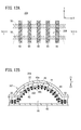
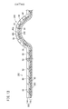
- FIG. 2 is a cross-sectional view taken along line II-II shown in FIG. It is a cross-section figure of a conductive film which constitutes a part of touch sensor concerning a 1st embodiment.
- FIG. 4 is a schematic plan view of the conductive film shown in FIG. 3.
- FIG. 5A is a partially enlarged view of the three-dimensional part shown in FIG.
- FIG. 5B is a cross-sectional view along the line VB-VB shown in FIG. 5A. It is typical sectional drawing in a flat part and a solid part.
- 7A and 7B are schematic explanatory diagrams relating to a method for forming a conductive film.
- FIG. 1 is a cross-sectional view taken along line II-II shown in FIG.
- FIG. 4 is a schematic plan view of the conductive film shown in FIG. 3.
- FIG. 5A is a partially enlarged view of the three-dimensional part shown in FIG.
- FIG. 5B is a cross-sectional view along
- FIG. 8A is a schematic cross-sectional view of a conductive film according to a first modification.
- FIG. 8B is a schematic cross-sectional view of a conductive film according to a second modification. It is a fragmentary sectional view of the conductive film concerning the 3rd modification. It is a cross-section figure of the conductive film which constitutes a part of touch sensor concerning a 2nd embodiment.
- It is a schematic plan view of the conductive film shown in FIG. 12A is a partially enlarged view of the three-dimensional part shown in FIG. 12B is a cross-sectional view taken along line XIIB-XIIB shown in FIG. 12A. It is typical sectional drawing in a flat part and a solid part.
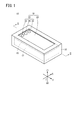
- FIG. 1 is a perspective view of a touch device 10 common to the embodiments, and FIG. 2 is a cross-sectional view taken along the line II-II shown in FIG.
- the touch device 10 includes a display 12 that displays arbitrary visible information, a touch sensor 16 that detects a position in contact with or close to the touch surface 14, and the display 12 and the touch sensor 16.
- a housing 18 is basically provided.
- the display device 12 is not particularly limited, and various display methods can be adopted. Suitable examples thereof include a liquid crystal panel, a plasma panel, an organic EL (Electro-Luminescence) panel, and an inorganic EL panel.
- the touch surface 14 includes a flat surface 20 that is planar and a solid surface 22 that is non-planar or curved.
- the three-dimensional surface 22 includes three hemispherical surfaces 23, 24, and 25 arranged along the X direction.
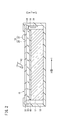
- the touch sensor 16 is electrically connected to the conductive film 30 via a conductive film 30, a cover member 32 laminated on one surface (arrow Z1 direction side) of the conductive film 30, and a cable 34. Connected substrate 36 and a control circuit 38 disposed on substrate 36.
- the conductive film 30 is adhered to one surface (arrow Z1 direction side) of the display 12 via the adhesive layer 40.
- the conductive film 30 is disposed on the display screen with the other main surface facing the display 12.
- the cover member 32 exhibits a function as the touch surface 14 by covering one surface of the conductive film 30.
- the contact body 42 for example, a finger or a stylus pen
- the material of the cover member 32 may be glass or a resin film, for example.
- the cover member 32 may be adhered to one surface of the conductive film 30 in a state where the cover member 32 is coated with silicon oxide or the like. Further, in order to prevent damage due to rubbing or the like, the conductive film 30 and the cover member 32 may be bonded together.
- the substrate 36 is an electronic substrate having flexibility. In this example, it is fixed to the inner wall of the side surface of the housing 18, but the arrangement position may be variously changed.
- the control circuit 38 captures a change in capacitance between the contact body 42 and the conductive film 30 when the contact body 42 that is a conductor contacts (or approaches) the touch surface 14, and detects the contact position ( Or the proximity position).
- FIG. 3 is a cross-sectional structural view of the conductive film 301 constituting a part of the touch sensor 16A according to the first embodiment
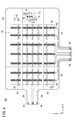
- FIG. 4 is a schematic plan view of the conductive film 301 shown in FIG.
- the conductive film 301 is formed on a flexible substrate 44 (substrate) and at least one surface of the flexible substrate 44 (here, both the first surface 46a and the second surface 46b). And a conductive portion 48. Note that this drawing shows only a portion corresponding to the flat surface 20 of FIG. 1 (flat portion 70 of FIG. 4).
- the conductive portion 48 formed on the first surface 46a side includes a plurality of upper electrodes 50 and lead wires 54 connected to the upper electrodes 50, respectively.
- the conductive portion 48 formed on the second surface 46b side includes a plurality of lower electrodes 60 and lead wires 64 connected to the lower electrodes 60, respectively.
- the upper electrode 50 is a detection electrode on the side closer to the touch surface 14 (FIG. 1) among the pair of electrodes included in the conductive film 301.
- the lower electrode 60 is a detection electrode on the side far from the touch surface 14 (FIG. 1) among the pair of electrodes provided in the conductive film 301.
- the upper electrode 50 and the lower electrode 60 are made of fine metal wires, and have a mesh pattern in which many cells having the same or different shapes are combined.
- the line width of the fine metal wire is preferably from 0.1 ⁇ m to 15 ⁇ m, more preferably from 0.5 ⁇ m to 9 ⁇ m, and still more preferably from 1 ⁇ m to 7 ⁇ m.
- a metal made of silver, copper, aluminum, gold, molybdenum, or an alloy containing one or more of these may be used as a material of the conductive portion 48.
- the flexible substrate 44 is made of a thermoplastic material, and is a substrate having insulation and transparency (approximately 85% or higher transmittance).
- the thickness of the flexible substrate 44 is preferably 20 to 350 ⁇ m, more preferably 30 to 250 ⁇ m, and still more preferably 40 to 200 ⁇ m.
- thermoplastic material is a material that has the property of softening by heating and solidifying when cooled, and the plasticity is reversibly maintained when cooling and heating are repeated.
- a resin material having excellent heat resistance, chemical resistance, and electrical insulation under a normal use environment is used.
- polyesters such as polyethylene terephthalate (PET) and polyethylene naphthalate (PEN); polyolefins such as polyethylene (PE), polypropylene (PP), polystyrene, and polyethylene vinyl acetate (EVA) kindss: Vinyl resin;
- PET polyethylene terephthalate
- PEN polyethylene naphthalate
- EVA polyethylene vinyl acetate
- Vinyl resin Vinyl resin
- PC polycarbonate
- PC polyamide
- polyimide acrylic resin
- TAC triacetyl cellulose
- COP cycloolefin polymer
- an extraction wiring 54 is electrically connected to one end portion of each upper electrode 50 through a connection portion 52.
- the lead wires 54 formed integrally with the plurality of upper electrodes 50 are routed toward a substantially central portion of one side extending along the Y direction, and are electrically connected to the terminal portion 56.
- the terminal part 56 is electrically connected to the control circuit 38 (FIG. 3).
- the plurality of upper electrodes 50 are each composed of a thin metal wire and have a plurality of strip-like patterns extending in the X direction (first direction).
- the upper electrode 50 has a predetermined width direction dimension toward the Y direction (second direction orthogonal to the first direction), and a plurality of the upper electrodes 50 are arranged along the Y direction.
- a lead wire 64 is electrically connected to one end portion of each lower electrode 60 through a connection portion 62.
- the lead wiring 64 formed integrally with the plurality of lower electrodes 60 is routed toward a substantially central portion of one side extending along the X direction and is electrically connected to the terminal portion 66.
- the terminal part 66 is electrically connected to the control circuit 38 (FIG. 3).
- the plurality of lower electrodes 60 are each composed of a thin metal wire and have a plurality of strip-like patterns extending in the Y direction (second direction).
- the lower electrode 60 has a predetermined width direction dimension toward the X direction (first direction), and a plurality of the lower electrodes 60 are arranged side by side along the X direction.
- a mesh pattern composed of fine metal wires is provided so as to be electrically insulated from each upper electrode 50 (or each lower electrode 60).
- a dummy electrode (not shown) may be provided. Specifically, the visibility of the touch sensor 16 can be improved by arranging the dummy electrodes so that the two-dimensional distribution of the electrode pattern is substantially uniform.
- the conductive film 301 has a flat portion 70 corresponding to the flat surface 20 (FIG. 1) and a three-dimensional portion 72 corresponding to the three-dimensional surface 22 (the same drawing). According to FIG. 1, although there are three three-dimensional parts 72, only one is drawn for convenience of illustration. Although not shown, the first electrode 76 is connected to the terminal portion 56, and the second electrode 78 is connected to the terminal portion 66.
- the upper electrode 50 and the lower electrode 60 are two-dimensionally arranged to form a planar detection region (hereinafter referred to as a planar region 74).
- the first electrode 76 and the second electrode 78 are three-dimensionally arranged to form a non-planar or curved detection region (hereinafter referred to as a three-dimensional region 80). That is, the touch operation detection area 82 includes a plane area 74 and a three-dimensional area 80.
- the three-dimensional part 72 corresponds to a part constituting the three-dimensional region 80 that is at least a part of the detection region 82.
- the conductive film 301 has a three-dimensional portion 72 that is convex toward the touch surface 14.
- the “convex shape” means a shape protruding from a reference surface (here, the plane formed by the flat portion 70), and may be configured by one curved surface, or a plane or a combination of curved surfaces.
- FIG. 5A is a partially enlarged view of the three-dimensional part 72 shown in FIG. 4
- FIG. 5B is a cross-sectional view taken along line VB-VB shown in FIG. 5A
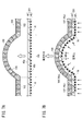
- FIG. 6 is a schematic view of the flat part 70 and the three-dimensional part 72. It is sectional drawing.
- a first electrode 76 and a second electrode 78 are formed in the three-dimensional region 80 so as to face each other.
- the first electrode 76 and the second electrode 78 are electrically insulated by being separated via a gap 84.
- the first electrode 76 and the second electrode 78 have a pattern in which a large number of cells 86 are combined.
- each cell 86 means a shape two-dimensionally partitioned by a plurality of fine metal wires.
- Each cell 86 is configured by a polygon including a triangle, a quadrangle (more specifically, a square, a rectangle, a parallelogram, a rhombus), a pentagon, and a hexagon.
- the shape of each cell 86 may be one or more, and the arrangement of each cell 86 may be regular or irregular.
- the length of one side of the cell 86 is preferably 100 to 300 ⁇ m.
- the first electrode 76 has a strip-shaped portion 88 extending along the X direction and an island-shaped portion 90 provided on the tip side of the strip-shaped portion 88.
- the second electrode 78 includes a band-shaped portion 92 extending along the X direction, and a surrounding portion 94 that is provided on the distal end side of the band-shaped portion 88 and surrounds a part of the island-shaped portion 90.
- the first electrode 76 / second electrode 78, the flexible substrate 44, and the cover member 32 are laminated in this order from the adhesive layer 40 in the direction of the arrow Z1. ing.
- a space portion 96 surrounded by a curved surface formed by the conductive film 301 and a plane formed by the adhesive layer 40 is formed.
- the conductive portions 48 are provided on both surfaces (the first surface 46 a and the second surface 46 b) of the flexible substrate 44.
- the conductive portions 48 are provided on both surfaces of the flexible substrate 44 in at least a part of the detection region 82 excluding the three-dimensional portion 72 (specifically, the planar region 74).
- the conductive part 48 is provided only on one surface (second surface 46 b) of the flexible substrate 44.
- the shielding electrode (not shown) made of a conductive material on the first surface 46a around the three-dimensional part 72.
- the shielding electrode may be formed of a mesh pattern made of fine metal wires or a solid metal pattern.
- the conductive portion 48 is formed on at least one surface of the planar flexible substrate 44.
- etching using a photolithography process, a microcontact printing patterning method, or a silver salt method can be employed.
- the “micro contact printing patterning method” is a method for obtaining a pattern having a narrow line width by using the micro contact printing method.
- the microcontact printing method is a method for producing a monomolecular film pattern by using an elastic polydimethylsiloxane stamp and bringing a thiol solution into contact with a gold base material as an ink (Whitedesed, Angew. Chem. Int. Ed., 1998, volume 37, page 550).
- a typical process of this method is described in detail in paragraph ⁇ 0104> of JP-T-2012-519329, for example.
- the substrate is coated with a metal (eg, silver is sputter coated onto a PET substrate).
- a metal eg, silver is sputter coated onto a PET substrate.
- masking of the monomolecular film is stamped using a microcontact printing method on a metal coated substrate.
- the metal coated on the substrate is removed by etching except for the pattern under masking.
- the “silver salt method” is to obtain a pattern of fine metal wires in a mesh shape by exposing and developing a photosensitive material having a photosensitive silver salt-containing layer. Specific operations thereof are described in detail in paragraphs ⁇ 0163> to ⁇ 0241> of JP2009-4348A.
- the upper electrode 50, the connection portion 52, the lead-out wiring 54, and the terminal portion 56 are integrally formed on the first surface 46a of the flexible substrate 44.
- the lower electrode 60, the connection part 62, the lead wiring 64, the terminal part 66, the first electrode 76, and the second electrode 78 are integrally formed on the second surface 46 b of the flexible substrate 44.
- the conductive portion 48 made of the same material in the same process, it is possible to prevent a decrease in yield and appearance due to the three-dimensional molding, and the degree of freedom in designing the electrode pattern and wiring. Becomes higher.
- the conductive portion 48 is formed only on one surface (second surface 46 b) of the flexible substrate 44 at a portion corresponding to the three-dimensional portion 72 (hereinafter, the corresponding portion 108) formed in the subsequent second step. Please note that.
- the planar conductive film 301 is vacuum formed into a three-dimensional shape along the three-dimensional surface 22 of the cover member 32.
- an outline of this molding method will be described with reference to FIGS. 7A and 7B.
- a flat surface 102 corresponding to the flat portion 70 in FIG. 6 and a three-dimensional surface 104 corresponding to the three-dimensional portion 72 are formed inside the molding die 100, respectively.
- a number of suction holes 106 penetrating in the thickness direction are formed in the molding die 100.
- the conductive film 301 is pressed against the inside of the molding die 100.
- the flexible substrate 44 is made of a thermoplastic material, the flexible substrate 44 is in a softened state by heating above a predetermined temperature (specifically, a softening temperature).
- a vacuum is drawn from the molding die 100 through the suction hole 106, and 0.000 from the conductive film 301 side.
- An air pressure of 1 to 2 MPa is applied.
- the corresponding portion 108 where the flexible substrate 44 is softened is deformed into a convex shape along the three-dimensional surface 104.
- the flexible substrate 44 is solidified by cooling below the softening temperature, and the convex shape is maintained under a normal use environment.
- the solid substrate 72 is formed by heating the integrated flexible substrate 44 and the conductive portion 48, and the conductive film 301 constituting the touch sensor 16A is completed.
- the conductive film 301 and the control circuit 38 are electrically connected via the cable 34, whereby the touch sensor 16A is completed.
- the touch sensor 16 ⁇ / b> A includes the conductive film 301 having the flexible substrate 44 and the conductive portion 48.
- the conductive portion 48 is provided on at least one surface (the first surface 46a and the second surface 46b) of the flexible substrate 44, and is provided with a plurality of detection electrodes arranged in the detection region 82, and the plurality of detection electrodes.
- the lead wires 54 and 64 are connected to each other.
- the “plurality of detection electrodes” correspond to the upper electrode 50, the lower electrode 60, the first electrode 76, and the second electrode 78.
- the flexible substrate 44 is made of a thermoplastic material, and the plurality of detection electrodes are each made of a thin metal wire.
- the conductive film 301 is formed with a three-dimensional portion 72 that is non-planar or curved in at least a part of the detection region 82 (three-dimensional region 80). In the three-dimensional portion 72, one side of the flexible substrate 44 is formed.
- the conductive portion 48 is provided only on the (second surface 46b).
- the conductive portion 48 is provided only on the second surface 46b of the flexible substrate 44 in the three-dimensional portion 72 of the conductive film 301, even if the flexible substrate 44 is deformed in the surface direction or the thickness direction (z direction).
- the distance between the first electrode 76 and the second electrode 78 hardly changes.
- the flexible substrate 44 is made of a thermoplastic material, and the first electrode 76 and the second electrode 78 are each made of a thin metal wire, the first electrode 76 and the second electrode made of a thin metal wire rich in flexibility.
- the electrode 78 is deformed substantially uniformly and substantially uniformly following the deformation of the flexible substrate 44 along the surface direction. As a result, even if the touch surface 14 has a three-dimensional shape, it is possible to suppress fluctuations in the electrical property value due to the detection electrodes, in other words, sufficient in-plane uniformity of sensor sensitivity can be ensured.
- the degree of deformation of the detection electrodes existing on each surface tends to be different. That is, when the relative positions of the detection electrodes are deviated, moire (interference fringes) is generated at a portion where the detection electrodes overlap in plan view, and the visibility of the conductive film 301 is reduced. In particular, it has been found that the influence appears remarkably when the detection electrode is formed of a thin metal wire. Since the distance between the first electrode 76 and the second electrode 78 is designed to be short, even when the three-dimensional part 72 is formed, the positional deviation from the design value is reduced, and the visibility is reduced due to moire. The suppression effect can also be expected.
- one surface of the flexible substrate 44 may be one surface (second surface 46b) opposite to the touch surface 14 (first surface 46a) of the touch sensor 16A.
- the first electrode 76 and the second electrode 78 can be physically protected because the flexible substrate 44 is interposed during the touch by the contact body 42.
- a convex three-dimensional part 72 may be formed on the conductive film 301 toward the touch surface 14.
- a three-dimensional touch sensor can be provided, and variations in touch operations increase.
- FIG. 8A is a schematic cross-sectional view of the conductive film 301a according to the first modification, and corresponds to the drawing content of FIG. As understood from this drawing, the configuration differs from the configuration of the conductive film 301 in that the conductive portion 48 is provided only on one side (second surface 46 b) of the flexible substrate 44.
- the upper electrode 50 (first electrode), the insulating layer 110, and the lower electrode 60 (second electrode) are laminated in order from the second surface 46b.
- the flexible substrate 44 By providing the conductive portion 48 only on one side of the flexible substrate 44 (opposite side of the touch surface 14), the flexible substrate 44 itself has a function of protecting the conductive portion 48. That is, the first surface 46a can be the touch surface 14, and as a result, the cover member 32 can be omitted.
- the insulating layer 110 is provided in a region that covers all or only a part of the conductive portion 48.
- a part of the conductive portion 48 for example, a region where the upper electrode 50 and the lower electrode 60 overlap in plan view may be used.
- a material of the insulating layer 110 for example, an organic material containing a photocurable resin or an inorganic material containing silicon oxide can be used.
- the thickness of the insulating layer 110 is preferably 0.1 to 10 ⁇ m.
- FIG. 8B is a schematic cross-sectional view of the conductive film 301b according to the second modification, and corresponds to the drawing content of FIG. Similar to FIG. 8A, the configuration differs from the configuration of the conductive film 301 in that the conductive portion 48 is provided only on one surface (second surface 46 b) of the flexible substrate 44.
- the first electrode 76 and the second electrode 78 are alternately arranged on the second surface 46b while being spaced apart at a constant interval.
- the insulating layer 110 it is not necessary to provide the insulating layer 110 separately, which is preferable from the viewpoint of production cost.
- FIG. 9 is a partial cross-sectional view of the conductive film 301c according to the third modification, and corresponds to the drawing content of FIG. 5B.
- the conductive portion 48 that is, the first electrode 76 and the second electrode 78
- the conductive portion 48 is provided only on the other surface (first surface 46a) of the flexible substrate 44, This is different from the configuration of the conductive film 301.
- the sensor sensitivity of the touch sensor 16A is improved.
- the conductive film 301c is three-dimensionally formed, the deformation amount on the outer surface side (first surface 46a) is relatively larger than that on the inner surface side (second surface 46b). Note that the impact will increase.
- a protective layer that covers the conductive portion 48 may be provided on one side (second surface 46b) side of the three-dimensional portion 72.
- FIG. 10 is a cross-sectional structural view of the conductive film 302 constituting a part of the touch sensor 16B according to the second embodiment
- FIG. 11 is a schematic plan view of the conductive film 302 shown in FIG.
- the conductive film 302 includes a flexible substrate 44 and a conductive portion 48 formed on one side (here, the second surface 46 b side) of the flexible substrate 44. Note that this drawing shows only a portion corresponding to the flat surface 20 in FIG. 1 (flat portion 202 in FIG. 11).
- the conductive portion 48 formed on the second surface 46b side includes a plurality of upper electrodes 50, lead wires 54 connected to the upper electrodes 50, a plurality of lower electrodes 60, and leads connected to the lower electrodes 60, respectively.
- the wiring 64 is included.
- An insulating layer 200 made of an insulating material is provided between the upper electrode 50 and the lead wiring 54 (first conductive layer) and the lower electrode 60 and the lead wiring 64 (second conductive layer).
- the insulating layer 200 may be provided in a region that covers all or only a part of the conductive portion 48 as in the case of the first modification (insulating layer 110).
- the conductive film 302 includes a first electrode 76 and a second electrode 78 (FIG. 4) in place of the first electrode 76 and the second electrode 78. It differs from the configuration of one embodiment (conductive film 301).
- the conductive film 302 has a flat portion 202 corresponding to the flat surface 20 (FIG. 1) and a three-dimensional portion 204 corresponding to the three-dimensional surface 22 (the same drawing).
- the upper electrode 50 and the lower electrode 60 are two-dimensionally arranged to form a planar detection region (hereinafter referred to as a planar region 206).
- the upper electrode 50 and the lower electrode 60 are three-dimensionally arranged to form a non-planar or curved detection region (hereinafter referred to as a three-dimensional region 208). That is, the touch operation detection area 210 includes a plane area 206 and a three-dimensional area 208.
- FIG. 12A is a partially enlarged view of the three-dimensional portion 204 shown in FIG. 11
- FIG. 12B is a cross-sectional view taken along the line XIIB-XIIB shown in FIG. 12A
- FIG. 13 is a schematic view of the flat portion 202 and the three-dimensional portion 204. It is sectional drawing.
- a plurality of upper electrodes 50 and a plurality of lower electrodes 60 are formed in the three-dimensional region 208 so as to intersect with each other as in the planar region 206 of FIG.
- the lower electrode 60, the insulating layer 200, the upper electrode 50, the flexible substrate 44, and the cover member 32 are sequentially arranged from the adhesive layer 40 in the direction of the arrow Z ⁇ b> 1. Are stacked.
- the conductive portion 48 is provided only on one surface (second surface 46 b) of the flexible substrate 44.
- the amount of displacement of the relative position between the upper electrode 50 and the lower electrode 60 in the three-dimensional part 204 is reduced. Can prevent moiré from occurring.
- the touch sensor 16 ⁇ / b> B includes the conductive film 302 having the flexible substrate 44 and the conductive portion 48.
- the conductive portion 48 is provided on at least one surface (second surface 46b) of the flexible substrate 44, and has a plurality of detection electrodes arranged in the detection region 210, and a lead connected to each of the plurality of detection electrodes. Wirings 54 and 64 are included.
- the “plurality of detection electrodes” correspond to the upper electrode 50 and the lower electrode 60.
- the conductive film 302 is formed with a three-dimensional portion 204 that is non-planar or curved in at least a part of the detection region 210 (three-dimensional region 208). In the three-dimensional portion 204, one side of the flexible substrate 44 is formed. The conductive portion 48 is provided only on the (second surface 46b). Even if comprised in this way, it cannot be overemphasized that the effect similar to the case of 1st Embodiment is acquired.
- the detection areas 82 and 210 include the planar areas 74 and 206, but all the detection areas may be non-planar or curved.
Landscapes
- Engineering & Computer Science (AREA)
- General Engineering & Computer Science (AREA)
- Theoretical Computer Science (AREA)
- Human Computer Interaction (AREA)
- Physics & Mathematics (AREA)
- General Physics & Mathematics (AREA)
- Position Input By Displaying (AREA)
Abstract
タッチ面が立体形状であってもセンサ感度の面内均一性を十分に確保可能なタッチセンサ、タッチデバイス及びタッチセンサの製造方法を提供する。可撓性基板44は熱可塑性材料で、複数の検出電極(上方電極50、下方電極60、第1電極76、及び第2電極78)は金属細線でそれぞれ構成される。導電性フィルム301及び302には、検出領域82及び210の少なくとも一部であって非平面状又は曲面状である立体領域80及び208を構成する立体部72及び204が形成される。立体部72及び204では、可撓性基板44の片面(第2面46b)のみに導電部48が設けられる。
Description
この発明は、導電性フィルムを備えるタッチセンサ、タッチデバイス及びタッチセンサの製造方法に関する。
近時、タッチセンサを組み込んだ電子機器が広く普及している。タッチセンサは、携帯電話やPDA(Personal Digital Assistant)等の小サイズ画面を備える電子機器に多く搭載されている。例えば、タッチ面の形状が立体であるタッチセンサが提案されている(特許文献1及び特許文献2を参照)。そして、この種のタッチセンサを作製する際、基板の主面上に複数の検出電極が設けられてなる、平面状の導電性フィルムを屈曲させながら立体的に成形する工程が含まれ得る。
ところで、本発明者の鋭意検討によれば、導電性フィルムの変形に伴い、検出電極間の距離(厚み方向及び面方向)が局所的に変化し、電気的物性値(静電容量、電気抵抗等)の変動が生じ得ることを見出した。特に、基板の両面上に検出電極をそれぞれ配置する場合、電気的物性値の不均一性が大きくなる傾向があった。
この現象により、タッチセンサの感度特性にローカリティ(局所的な面内不均一性)が発生することが懸念されるが、特許文献1及び特許文献2には上記した問題点及びその解決策について何ら言及されていない。
本発明は上記した課題を解決するためになされたものであり、タッチ面が立体形状であってもセンサ感度の面内均一性を十分に確保可能なタッチセンサ、タッチデバイス及びタッチセンサの製造方法を提供することを目的とする。
本発明に係るタッチセンサは、基板と、上記基板の少なくとも一面に設けられ、且つ、上記少なくとも一面の検出領域内に配置された複数の検出電極、及び上記複数の検出電極にそれぞれ接続された引出配線を含む導電部とを有する導電性フィルムを備え、上記基板は熱可塑性材料で、上記複数の検出電極は金属細線でそれぞれ構成され、上記導電性フィルムには、上記検出領域の少なくとも一部であって非平面状又は曲面状である立体領域を構成する立体部が形成され、上記立体部では、上記基板の片面のみに上記導電部が設けられる。
このように、導電性フィルムの立体部にて基板の片面のみに導電部を設けたので、基板が変形されても検出電極間の距離は殆ど変化しない。また、基板は熱可塑性材料で、複数の検出電極は金属細線でそれぞれ構成されているので、柔軟性に富む金属細線で構成された複数の検出電極は、面方向に沿った熱可塑性基板の変形にならって略均等・略均質に変形する。これらにより、タッチ面が立体形状であっても検出電極による電気的物性値の変動を抑止可能となり、換言すれば、センサ感度の面内均一性を十分に確保できる。
また、基板の両面に検出電極を設けた場合、各面に存在する検出電極の変形度が異なる傾向がある。つまり、検出電極の相対位置がずれた場合、各検出電極が平面視で重なる部位にてモアレ(干渉縞)が発生し、導電性フィルムの視認性が低下する。特に、検出電極が金属細線で構成された場合にその影響が顕著に現われることが分かった。本発明によれば、検出電極間の距離が短くなるように設計しているので、立体部を形成した場合であっても設計値からの位置ずれが少なくなり、モアレによる視認性低下を抑制する効果も期待できる。
また、上記片面は、上記タッチセンサのタッチ面と反対側の一面であることが好ましい。
また、上記導電性フィルムには、上記タッチ面に向かって凸状の上記立体部が形成されることが好ましい。
また、上記立体部に設けられた上記導電部は、上記片面から上記基板方向に向かって順に、第1電極、絶縁層及び第2電極が配置されてなることが好ましい。
また、上記立体部の上記片面側には、上記導電部を被覆する保護層が設けられることが好ましい。
また、上記引出配線は、上記複数の検出電極と一体的に形成されていることが好ましい。
また、上記立体部を除く上記検出領域の少なくとも一部の領域にて、上記基板の両面に上記導電部が設けられることが好ましい。
本発明に係るタッチデバイスは、上記したいずれかのタッチセンサと、表示画面上に上記タッチセンサが設けられた表示器とを備える。
本発明は、基板と、上記基板の少なくとも一面に設けられ、且つ、上記少なくとも一面の検出領域内に配置された複数の検出電極、及び上記複数の検出電極にそれぞれ接続された引出配線を含む導電部とを有する導電性フィルムを備えるタッチセンサの製造方法に関し、熱可塑性材料で構成される上記基板上に金属細線で構成される上記導電部を形成する第1工程と、一体となった上記基板及び上記導電部を加熱することで、上記検出領域の少なくとも一部であって非平面状又は曲面状である立体領域を構成する立体部を形成する第2工程とを備え、上記第1工程では、上記立体部の相当部位にて上記基板の片面のみに上記導電部を形成する。
本発明に係るタッチセンサ、タッチデバイス及びタッチセンサの製造方法によれば、導電性フィルムの立体部にて基板の片面のみに導電部を設けたので、基板が変形されても検出電極間の距離は殆ど変化しない。また、基板は熱可塑性材料で、複数の検出電極は金属細線でそれぞれ構成されているので、柔軟性に富む金属細線で構成された複数の検出電極は、面方向に沿った熱可塑性基板の変形にならって略均等・略均質に変形する。これらにより、タッチ面が立体形状であっても検出電極による電気的物性値の変動を抑止可能となり、換言すれば、センサ感度の面内均一性を十分に確保できる。
また、基板の両面に検出電極を設けた場合、各面に存在する検出電極の変形度が異なる傾向がある。つまり、検出電極の相対位置がずれた場合、各検出電極が平面視で重なる部位にてモアレが発生し、導電性フィルムの視認性が低下する。特に、検出電極が金属細線で構成された場合にその影響が顕著に現われることが分かった。本発明によれば、検出電極間の距離が短くなるように設計しているので、立体部を形成した場合であっても設計値からの位置ずれが少なくなり、モアレによる視認性低下を抑制する効果も期待できる。
以下、本発明に係るタッチセンサについてその製造方法及びタッチデバイスとの関係において好適な実施形態を挙げ、添付の図面を参照しながら詳細に説明する。なお、本明細書において数値範囲を示す「~」は、その前後に記載される数値を下限値及び上限値として含む意味として使用される。
[タッチデバイス10の構成]
図1は各実施形態に共通するタッチデバイス10の斜視図であり、図2は図1に示すII-II線に沿った断面図である。
図1は各実施形態に共通するタッチデバイス10の斜視図であり、図2は図1に示すII-II線に沿った断面図である。
図1に示すように、タッチデバイス10は、任意の可視情報を表示する表示器12と、タッチ面14から接触又は近接する位置を検出するタッチセンサ16と、表示器12及びタッチセンサ16を収容する筐体18とを基本的に備える。
表示器12は、特に限定されるものではなく種々の表示方式を採用できる。その好適な例としては、液晶パネル、プラズマパネル、有機EL(Electro-Luminescence)パネル、無機ELパネル等が挙げられる。
タッチ面14は、平面状である平坦面20と、非平面状又は曲面状である立体面22とから構成される。本図例では、立体面22は、X方向に沿って配された3つの半球面23、24及び25からなる。
図2に示すように、タッチセンサ16は、導電性フィルム30と、導電性フィルム30の一面(矢印Z1方向側)に積層されたカバー部材32と、ケーブル34を介して導電性フィルム30に電気的に接続された基板36と、基板36上に配置された制御回路38とを備える。
表示器12の一面(矢印Z1方向側)には、接着層40を介して、導電性フィルム30が接着されている。導電性フィルム30は、他方の主面側を表示器12に対向させながら表示画面上に配置されている。
カバー部材32は、導電性フィルム30の一面を被覆することで、タッチ面14としての機能を発揮する。また、接触体42(例えば、指やスタイラスペン)による直接的な接触を防止することで、擦り傷の発生や、塵埃の付着等を抑止可能であり、導電性フィルム30の導電特性を安定させることができる。
カバー部材32の材質は、例えば、ガラス、又は樹脂フィルムであってもよい。カバー部材32を酸化珪素等でコートした状態で、導電性フィルム30の一面に密着させてもよい。また、擦れ等による損傷を防止するため、導電性フィルム30及びカバー部材32を貼り合わせて構成してもよい。
基板36は、可撓性を備える電子基板である。本図例では、筐体18の側面内壁に固定されているが、配設位置は種々変更してもよい。制御回路38は、導体である接触体42をタッチ面14に接触(又は近接)する際、接触体42と導電性フィルム30との間での静電容量の変化を捉えて、その接触位置(又は近接位置)を検出する。
[第1実施形態]
先ず、第1実施形態に係るタッチセンサ16A(タッチセンサ16の一形態)の構成について、図3~図7Bを参照しながら説明する。
先ず、第1実施形態に係るタッチセンサ16A(タッチセンサ16の一形態)の構成について、図3~図7Bを参照しながら説明する。
<タッチセンサ16Aの構成>
図3は第1実施形態に係るタッチセンサ16Aの一部を構成する導電性フィルム301の断面構造図であり、図4は図3に示す導電性フィルム301の概略平面図である。
図3は第1実施形態に係るタッチセンサ16Aの一部を構成する導電性フィルム301の断面構造図であり、図4は図3に示す導電性フィルム301の概略平面図である。
図3に示すように、導電性フィルム301は、可撓性基板44(基板)と、可撓性基板44の少なくとも一面(ここでは、第1面46a及び第2面46bの両面)に形成された導電部48とを有する。なお、本図は、図1の平坦面20に対応する部位(図4の平坦部70)のみを表記している。
第1面46a側に形成された導電部48は、複数の上方電極50と、上方電極50にそれぞれ接続された引出配線54とを含んで構成される。第2面46b側に形成された導電部48は、複数の下方電極60と、下方電極60にそれぞれ接続された引出配線64とを含んで構成される。上方電極50は、導電性フィルム301が備える一対の電極のうちタッチ面14(図1)から近い側の検出電極である。一方、下方電極60は、導電性フィルム301が備える一対の電極のうちタッチ面14(図1)に遠い側の検出電極である。
上方電極50及び下方電極60は、金属細線で構成されており、同一の又は異なる形状のセルを多数組み合わせたメッシュパターンを有する。金属細線の線幅は0.1μm以上15μm以下が好ましく、0.5μm以上9μm以下がより好ましく、1μm以上7μm以下が更に好ましい。導電部48の材料として、銀、銅、アルミニウム、金、モリブデン又はこれらの中の1種以上を含む合金等からなる金属を用いてもよい。
可撓性基板44は、熱可塑性材料で構成されており、絶縁性及び透明性(概ね85%以上の透過率)を有する基板である。可撓性基板44の厚みは20~350μmが好ましく、30~250μmがより好ましく、40~200μmが更に好ましい。
ここで、「熱可塑性材料」とは、加熱により軟化し、その後に冷却すると固化する性質を有し、かつ、冷却及び加熱を繰り返した場合に塑性が可逆的に保たれる材料である。例えば、通常の使用環境下における耐熱性、耐薬品性及び電気絶縁性に優れた樹脂材料が使用される。
プラスチックフィルム及びプラスチック板の原料としては、例えば、ポリエチレンテレフタレート(PET)、ポリエチレンナフタレート(PEN)等のポリエステル類;ポリエチレン(PE)、ポリプロピレン(PP)、ポリスチレン、ポリエチレンビニルアセテート(EVA)等のポリオレフィン類;ビニル系樹脂;その他、ポリカーボネート(PC)、ポリアミド、ポリイミド、アクリル樹脂、トリアセチルセルロース(TAC)、シクロオレフィンポリマー(COP)等を用いることができる。
図4に示すように、各上方電極50の一端部には、結線部52を介して引出配線54が電気的に接続される。複数の上方電極50と一体的に形成された引出配線54は、Y方向に沿って延在する一辺の略中央部に向かって引き回され、端子部56に電気的に接続されている。端子部56は、制御回路38(図3)に電気的に接続される。
複数の上方電極50は、金属細線でそれぞれ構成されており、X方向(第1方向)に延びる複数の帯状のパターンを有する。上方電極50は、Y方向(第1方向と直交する第2方向)に向かう所定の幅方向寸法を有すると共に、Y方向に沿って複数並んで配置されている。
各下方電極60の一端部には、結線部62を介して引出配線64が電気的に接続される。複数の下方電極60と一体的に形成された引出配線64は、X方向に沿って延在する一辺の略中央部に向かって引き回され、端子部66に電気的に接続されている。端子部66は、制御回路38(図3)に電気的に接続される。
複数の下方電極60は、金属細線でそれぞれ構成されており、Y方向(第2方向)に延びる複数の帯状のパターンを有する。下方電極60は、X方向(第1方向)に向かう所定の幅方向寸法を有すると共に、X方向に沿って複数並んで配置されている。
隣接する上方電極50(或いは、下方電極60)の間の領域に、各上方電極50(或いは、各下方電極60)と電気的に絶縁されるように、金属細線で構成されたメッシュパターンを有するダミー電極(図示せず)を設けてもよい。具体的には、電極パターンの二次元分布が略均一化されるようにダミー電極を配置することで、タッチセンサ16の視認性を向上することができる。
導電性フィルム301は、平坦面20(図1)に対応する平坦部70と、立体面22(同図)に対応する立体部72とを有する。図1によれば、立体部72は3つ存在するが、図示の便宜のため1つのみを描画している。また、図示を省略しているが、第1電極76は端子部56に接続されており、かつ、第2電極78は端子部66に接続されている。
平坦部70には、上方電極50及び下方電極60が二次元的に配置されることで、平面状の検出領域(以下、平面領域74という)が形成される。立体部72には、第1電極76及び第2電極78が三次元的に配置されることで、非平面状又は曲面状の検出領域(以下、立体領域80という)が形成される。すなわち、タッチ操作の検出領域82は、平面領域74及び立体領域80から構成される。換言すれば、立体部72は、検出領域82の少なくとも一部である立体領域80を構成する部位に相当する。
なお、導電性フィルム301には、タッチ面14に向かって凸状の立体部72が形成されている。「凸状」とは、基準面(ここでは、平坦部70が構成する平面)から突出している形状を意味し、1つの曲面、又は、平面若しくは曲面を組み合わせた面で構成されてもよい。
<立体部72の構成>
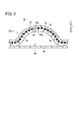
図5Aは図4に示す立体部72の部分拡大図であり、図5Bは図5Aに示すVB-VB線に沿った断面図であり、図6は平坦部70及び立体部72における模式的な断面図である。
図5Aは図4に示す立体部72の部分拡大図であり、図5Bは図5Aに示すVB-VB線に沿った断面図であり、図6は平坦部70及び立体部72における模式的な断面図である。
図5Aに示すように、立体領域80内には、第1電極76及び第2電極78が互いに対向して形成されている。第1電極76及び第2電極78は、隙間84を介して離間することで電気的に絶縁されている。第1電極76及び第2電極78は、多数のセル86を組み合わせたパターンを有する。
ここで、「セル」とは、複数の金属細線によって二次元的に区画された形状を意味する。各セル86は、例えば、三角形、四角形(より詳細には、正方形、長方形、平行四辺形、菱形)、五角形、六角形を含む多角形で構成されている。各セル86の形状の種類は1つ又は複数であってもよいし、各セル86の配置は規則的であっても不規則的であってもよい。セル86の一辺の長さは、100~300μmが好ましい。
第1電極76は、X方向に沿って延在する帯状部88と、帯状部88の先端側に設けられた島状部90とを有する。第2電極78は、X方向に沿って延在する帯状部92と、帯状部88の先端側に設けられ、島状部90の一部を囲む囲繞部94とを有する。
図5B及び図6に示すように、立体部72において、接着層40から矢印Z1方向に向かって順に、第1電極76/第2電極78、可撓性基板44、及びカバー部材32が積層されている。導電性フィルム301がなす曲面及び接着層40がなす平面に囲まれた空間部96が形成されている。
図6から理解されるように、導電性フィルム301の平坦部70では、可撓性基板44の両面(第1面46a及び第2面46b)に導電部48が設けられている。換言すれば、立体部72を除く検出領域82の少なくとも一部の領域(具体的には、平面領域74)にて、可撓性基板44の両面に導電部48が設けられている。一方、導電性フィルム301の立体部72では、可撓性基板44の片面(第2面46b)のみに導電部48が設けられている。
なお、立体部72の周辺にて、導電性材料で構成される遮蔽電極(図示せず)を第1面46a上に設けることが好ましい。この遮蔽電極は、例えば、金属細線から構成されるメッシュパターン、又は金属のベタパターンで形成してもよい。これによって、立体領域80の外側に向けて延びる配線(図5Aの帯状部88及び92)を接触体42から効果的に遮蔽可能となり、その結果、タッチセンサ16Aの誤動作を防止できる。
<タッチセンサ16Aの製造方法>
続いて、タッチセンサ16Aの製造方法について説明する。この製造方法は、後述するタッチセンサ16B(第2実施形態)にも同様に適用できる。
続いて、タッチセンサ16Aの製造方法について説明する。この製造方法は、後述するタッチセンサ16B(第2実施形態)にも同様に適用できる。
[1]第1工程において、平面状の可撓性基板44の少なくとも一面に導電部48を形成する。線幅が狭いパターンを得るために、フォトリソプロセスを使用したエッチング、マイクロコンタクト印刷パターニング法、又は銀塩法を採用できる。
「マイクロコンタクト印刷パターニング法」とは、マイクロコンタクト印刷法を利用して線幅が狭いパターンを得る方法である。ここで、マイクロコンタクト印刷法は、弾力性のあるポリジメチルシロキサンのスタンプを用い、チオール溶液をインキとして金基材に接触させて単分子膜のパターンを作製する方法である(Whitesedes著、Angew.Chem.Int.Ed.,1998年第37巻第550頁参照)。
この手法の代表的なプロセスは、例えば、特表2012-519329号公報の段落<0104>に詳述されている。先ず、基材に金属がコーティングされる(例えば、銀が、PET基材にスパッタコーティングされる)。次に、単分子膜のマスキングが、金属がコーティングされた基材にマイクロコンタクト印刷法を用いてスタンピングされる。その後、マスキング下のパターンを除いて、基材にコーティングされた金属がエッチングにより除去される。
「銀塩法」は、感光性銀塩含有層を有する感光材料を露光及び現像することにより、メッシュ状をなす金属細線のパターンを得るものである。その具体的な作業等は、特開2009-4348号公報の段落<0163>~<0241>に詳述されている。
これによって、可撓性基板44の第1面46a上に、上方電極50、結線部52、引出配線54、及び端子部56が一体的に形成される。同様に、可撓性基板44の第2面46b上に、下方電極60、結線部62、引出配線64、端子部66、第1電極76、及び第2電極78が一体的に形成される。
このように、同一の工程において、同一の材料からなる導電部48を一体的に形成することで、立体成形に起因する歩留まり・見栄えの低下を防止できると共に、電極パターン及び配線に関する設計の自由度が高くなる。
ここで、後の第2工程で形成される立体部72に相当する部位(以下、相当部位108)にて、可撓性基板44の片面(第2面46b)のみに導電部48が形成されている点に留意する。
[2]第2工程において、平面状の導電性フィルム301を、カバー部材32の立体面22に沿う三次元形状に真空成形する。以下、この成形方法の概略について、図7A及び図7Bを参照しながら説明する。
図7Aに示すように、成形用金型100の内側には、図6の平坦部70に相当する平坦面102、立体部72に相当する立体面104がそれぞれ形成されている。成形用金型100には、厚さ方向に貫通する吸引孔106が多数形成されている。例えば、平面状の導電性フィルム301のうち、少なくとも相当部位108を140~210℃に加熱した後、この導電性フィルム301を成形用金型100の内側に押し当てる。ここで、可撓性基板44は熱可塑性材料で構成されているので、所定温度(具体的には、軟化温度)を上回る加熱によって可撓性基板44は軟化した状態にある。
図7Bに示すように、導電性フィルム301を平坦面102及び立体面104に押し当てた状態下、成形用金型100から吸引孔106を介して真空に引き、導電性フィルム301側から0.1~2MPaの空気圧を付加する。そうすると、可撓性基板44が軟化した相当部位108は、立体面104に沿って凸状に変形させられる。その後、軟化温度を下回る冷却によって可撓性基板44は固化し、かつ、通常の使用環境下にて凸状が維持される。
このように、一体となった可撓性基板44及び導電部48を加熱することで立体部72を形成し、タッチセンサ16Aを構成する導電性フィルム301が完成する。
[3]第3工程において、ケーブル34を介して、導電性フィルム301と制御回路38を電気的に接続することで、タッチセンサ16Aは完成する。
<第1実施形態の構成及び効果>
以上のように、第1実施形態に係るタッチセンサ16Aは、可撓性基板44及び導電部48を有する導電性フィルム301を備える。導電部48は、可撓性基板44の少なくとも一面(第1面46a、第2面46b)に設けられ、且つ、検出領域82内に配置された複数の検出電極、及びこの複数の検出電極にそれぞれ接続された引出配線54及び64を含む。ここで、「複数の検出電極」は、上方電極50、下方電極60、第1電極76、及び第2電極78に相当する。
以上のように、第1実施形態に係るタッチセンサ16Aは、可撓性基板44及び導電部48を有する導電性フィルム301を備える。導電部48は、可撓性基板44の少なくとも一面(第1面46a、第2面46b)に設けられ、且つ、検出領域82内に配置された複数の検出電極、及びこの複数の検出電極にそれぞれ接続された引出配線54及び64を含む。ここで、「複数の検出電極」は、上方電極50、下方電極60、第1電極76、及び第2電極78に相当する。
可撓性基板44は熱可塑性材料で、複数の検出電極は金属細線でそれぞれ構成されている。そして、導電性フィルム301には検出領域82の少なくとも一部の領域(立体領域80)にて非平面状又は曲面状である立体部72が形成され、立体部72では可撓性基板44の片面(第2面46b)のみに導電部48が設けられる。
導電性フィルム301の立体部72にて可撓性基板44の第2面46bのみに導電部48を設けたので、面方向又は厚み方向(z方向)に可撓性基板44が変形されても第1電極76、第2電極78間の距離は殆ど変化しない。また、可撓性基板44は熱可塑性材料で、第1電極76、第2電極78は金属細線でそれぞれ構成されているので、柔軟性に富む金属細線で構成された第1電極76、第2電極78は、面方向に沿った可撓性基板44の変形にならって略均等・略均質に変形する。これらにより、タッチ面14が立体形状であっても検出電極による電気的物性値の変動を抑止可能となり、換言すれば、センサ感度の面内均一性を十分に確保できる。
また、可撓性基板44の両面に検出電極を設けた場合、各面に存在する検出電極の変形度が異なる傾向がある。つまり、検出電極の相対位置がずれた場合、各検出電極が平面視で重なる部位にてモアレ(干渉縞)が発生し、導電性フィルム301の視認性が低下する。特に、検出電極が金属細線で構成された場合にその影響が顕著に現われることが分かった。第1電極76、第2電極78間の距離が短くなるように設計しているので、立体部72を形成した場合であっても設計値からの位置ずれが少なくなり、モアレによる視認性低下を抑制する効果も期待できる。
また、可撓性基板44の片面は、タッチセンサ16Aのタッチ面14(第1面46a)と反対側の一面(第2面46b)であってもよい。接触体42によるタッチの際に可撓性基板44が介在することで、第1電極76、第2電極78を物理的に保護できる。
また、導電性フィルム301には、タッチ面14に向かって凸状の立体部72が形成されてもよい。これにより、立体形状のタッチセンサを提供可能になり、タッチ操作のバリエーションが増加する。
<変形例>
続いて、第1実施形態に係る導電性フィルム301の変形例について、図8A~図9を参照しながら説明する。なお、本実施形態と同一である構成要素には、同一の参照符号を付して詳細な説明を省略する。
続いて、第1実施形態に係る導電性フィルム301の変形例について、図8A~図9を参照しながら説明する。なお、本実施形態と同一である構成要素には、同一の参照符号を付して詳細な説明を省略する。
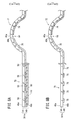
図8Aは、第1変形例に係る導電性フィルム301aの模式的な断面図であり、図6の描画内容に対応する。本図から理解されるように、可撓性基板44の片面(第2面46b)のみに導電部48が設けられている点で、導電性フィルム301の構成と異なっている。
具体的には、平坦部70では、第2面46bから順に、上方電極50(第1電極)、絶縁層110及び下方電極60(第2電極)が積層されている。可撓性基板44の片面(タッチ面14の反対側)のみに導電部48を設けることで、可撓性基板44自体が導電部48を保護する機能を担う。すなわち、第1面46aをタッチ面14とすることが可能になり、その結果、カバー部材32を省略することができる。
絶縁層110は、導電部48の全部又は一部のみを網羅する領域内に設けられる。導電部48の一部として、例えば、上方電極50及び下方電極60が平面視にて重なる領域であってもよい。絶縁層110の材料としては、例えば、光硬化性樹脂を含む有機材料や、酸化珪素を含む無機材料を用いることができる。絶縁層110の厚みは、0.1~10μmが好ましい。
図8Bは、第2変形例に係る導電性フィルム301bの模式的な断面図であり、図6の描画内容に対応する。図8Aと同様に、可撓性基板44の片面(第2面46b)のみに導電部48が設けられている点で、導電性フィルム301の構成と異なっている。
具体的には、平坦部70において、第2面46bの上には、第1電極76及び第2電極78(図5A等参照)が一定の間隔で離間しながら交互に配置されている。図8Aの構成と比較すると、絶縁層110を別途設ける必要がなく生産コストの観点で好適である。
図9は、第3変形例に係る導電性フィルム301cの部分断面図であり、図5Bの描画内容に対応する。本図から理解されるように、可撓性基板44の別の片面(第1面46a)のみに導電部48(すなわち、第1電極76及び第2電極78)が設けられている点で、導電性フィルム301の構成と異なっている。このように、立体面22に一層近い第1面46aに導電部48を設けることで、タッチセンサ16Aのセンサ感度が向上する。その反面、導電性フィルム301cを立体成形する際に、内面側(第2面46b)と比べて外面側(第1面46a)の変形量が相対的に大きくなり、その結果、導電部48に与える影響度が増加する点に留意する。
また、導電部48を物理的に保護することを目的として、立体部72の片面(第2面46b)側に導電部48を被覆する保護層を設けてもよい。
[第2実施形態]
続いて、第2実施形態に係るタッチセンサ16B(タッチセンサ16の一形態)の構成について、図10~図13を参照しながら説明する。
続いて、第2実施形態に係るタッチセンサ16B(タッチセンサ16の一形態)の構成について、図10~図13を参照しながら説明する。
<タッチセンサ16Bの構成>
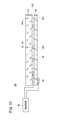
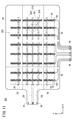
図10は第2実施形態に係るタッチセンサ16Bの一部を構成する導電性フィルム302の断面構造図であり、図11は図10に示す導電性フィルム302の概略平面図である。
図10は第2実施形態に係るタッチセンサ16Bの一部を構成する導電性フィルム302の断面構造図であり、図11は図10に示す導電性フィルム302の概略平面図である。
図10に示すように、導電性フィルム302は、可撓性基板44と、可撓性基板44の片面側(ここでは、第2面46b側)に形成された導電部48とを有する。なお、本図は、図1の平坦面20に対応する部位(図11の平坦部202)のみを表記している。
第2面46b側に形成された導電部48は、複数の上方電極50と、上方電極50にそれぞれ接続された引出配線54と、複数の下方電極60と、下方電極60にそれぞれ接続された引出配線64とを含んで構成される。なお、上方電極50及び引出配線54(第1導電層)と、下方電極60及び引出配線64(第2導電層)の間には、絶縁性材料からなる絶縁層200が設けられている。絶縁層200は、第1変形例(絶縁層110)の場合と同様に、導電部48の全部又は一部のみを網羅する領域内に設けてもよい。
図11に示すように、導電性フィルム302は、第1電極76及び第2電極78(図4)を欠く代わりに、上方電極50及び下方電極60の配置面積が広くなっている点で、第1実施形態(導電性フィルム301)の構成と異なっている。
導電性フィルム302は、平坦面20(図1)に対応する平坦部202と、立体面22(同図)に対応する立体部204とを有する。平坦部202には、上方電極50及び下方電極60が二次元的に配置されることで、平面状の検出領域(以下、平面領域206という)が形成される。立体部204には、上方電極50及び下方電極60が三次元的に配置されることで、非平面状又は曲面状の検出領域(以下、立体領域208という)が形成される。すなわち、タッチ操作の検出領域210は、平面領域206及び立体領域208から構成される。
<立体部204の構成>
図12Aは図11に示す立体部204の部分拡大図であり、図12Bは図12Aに示すXIIB-XIIB線に沿った断面図であり、図13は平坦部202及び立体部204における模式的な断面図である。
図12Aは図11に示す立体部204の部分拡大図であり、図12Bは図12Aに示すXIIB-XIIB線に沿った断面図であり、図13は平坦部202及び立体部204における模式的な断面図である。
図12Aに示すように、立体領域208内には、図11の平面領域206と同様に、複数の上方電極50及び複数の下方電極60が交差して形成されている。
図12B及び図13に示すように、立体部204において、接着層40から矢印Z1方向に向かって順に、下方電極60、絶縁層200、上方電極50、可撓性基板44、及びカバー部材32が積層されている。
図13から理解されるように、導電性フィルム302の平坦部202及び立体部204では、可撓性基板44の片面(第2面46b)のみに導電部48が設けられている。特に、絶縁層200の厚さを可撓性基板44よりも薄く設けることで、立体部204における上方電極50及び下方電極60の間の相対位置のずれ量が少なくなるので、両者の重なり領域にてモアレが発生するのを防止できる。
<第2実施形態の構成及び効果>
以上のように、第2実施形態に係るタッチセンサ16Bは、可撓性基板44及び導電部48を有する導電性フィルム302を備える。導電部48は、可撓性基板44の少なくとも一面(第2面46b)に設けられ、且つ、検出領域210内に配置された複数の検出電極、及びこの複数の検出電極にそれぞれ接続された引出配線54及び64を含む。ここで、「複数の検出電極」は、上方電極50及び下方電極60に相当する。
以上のように、第2実施形態に係るタッチセンサ16Bは、可撓性基板44及び導電部48を有する導電性フィルム302を備える。導電部48は、可撓性基板44の少なくとも一面(第2面46b)に設けられ、且つ、検出領域210内に配置された複数の検出電極、及びこの複数の検出電極にそれぞれ接続された引出配線54及び64を含む。ここで、「複数の検出電極」は、上方電極50及び下方電極60に相当する。
そして、導電性フィルム302には検出領域210の少なくとも一部の領域(立体領域208)にて非平面状又は曲面状である立体部204が形成され、立体部204では可撓性基板44の片面(第2面46b)のみに導電部48が設けられる。このように構成しても、第1実施形態の場合と同様の作用効果が得られることは言うまでもない。
[補足]
なお、この発明は、上述した実施形態に限定されるものではなく、この発明の主旨を逸脱しない範囲で自由に変更できることは勿論である。
なお、この発明は、上述した実施形態に限定されるものではなく、この発明の主旨を逸脱しない範囲で自由に変更できることは勿論である。
例えば、この実施形態では、検出領域82及び210には平面領域74及び206が含まれているが、すべての検出領域が非平面状又は曲面状であってもよい。
10…タッチデバイス 12…表示器
14…タッチ面 16、16A、16B…タッチセンサ
30、301(a~c)、302…導電性フィルム
32…カバー部材 38…制御回路
44…可撓性基板 46a…第1面
46b…第2面 48…導電部
50…上方電極 52、62…結線部
54、64…引出配線 56、66…端子部
60…下方電極 70、202…平坦部
72、204…立体部 74、206…平面領域
76…第1電極 78…第2電極
80、208…立体領域 82、210…検出領域
100…成形用金型 108…相当部位
110、200…絶縁層
14…タッチ面 16、16A、16B…タッチセンサ
30、301(a~c)、302…導電性フィルム
32…カバー部材 38…制御回路
44…可撓性基板 46a…第1面
46b…第2面 48…導電部
50…上方電極 52、62…結線部
54、64…引出配線 56、66…端子部
60…下方電極 70、202…平坦部
72、204…立体部 74、206…平面領域
76…第1電極 78…第2電極
80、208…立体領域 82、210…検出領域
100…成形用金型 108…相当部位
110、200…絶縁層
Claims (9)
- 基板と、
前記基板の少なくとも一面に設けられ、且つ、前記少なくとも一面の検出領域内に配置された複数の検出電極、及び前記複数の検出電極にそれぞれ接続された引出配線を含む導電部と
を有する導電性フィルムを備え、
前記基板は熱可塑性材料で、前記複数の検出電極は金属細線でそれぞれ構成され、
前記導電性フィルムには、前記検出領域の少なくとも一部であって非平面状又は曲面状である立体領域を構成する立体部が形成され、
前記立体部では、前記基板の片面のみに前記導電部が設けられる
ことを特徴とするタッチセンサ。 - 請求項1記載のタッチセンサにおいて、
前記片面は、前記タッチセンサのタッチ面と反対側の一面であるタッチセンサ。 - 請求項2記載のタッチセンサにおいて、
前記導電性フィルムには、前記タッチ面に向かって凸状の前記立体部が形成されるタッチセンサ。 - 請求項1~3のいずれか1項に記載のタッチセンサにおいて、
前記立体部に設けられた前記導電部は、前記片面から前記基板方向に向かって順に、第1電極、絶縁層及び第2電極が配置されてなるタッチセンサ。 - 請求項1~4のいずれか1項に記載のタッチセンサにおいて、
前記立体部の前記片面側には、前記導電部を被覆する保護層が設けられるタッチセンサ。 - 請求項1~5のいずれか1項に記載のタッチセンサにおいて、
前記引出配線は、前記複数の検出電極と一体的に形成されているタッチセンサ。 - 請求項1~6のいずれか1項に記載のタッチセンサにおいて、
前記立体部を除く前記検出領域の少なくとも一部の領域にて、前記基板の両面に前記導電部が設けられるタッチセンサ。 - 請求項1~7のいずれか1項に記載のタッチセンサと、表示画面上に前記タッチセンサが設けられた表示器とを備えることを特徴とするタッチデバイス。
- 基板と、前記基板の少なくとも一面に設けられ、且つ、前記少なくとも一面の検出領域内に配置された複数の検出電極、及び前記複数の検出電極にそれぞれ接続された引出配線を含む導電部とを有する導電性フィルムを備えるタッチセンサの製造方法であって、
熱可塑性材料で構成される前記基板上に金属細線で構成される前記導電部を形成する第1工程と、
一体となった前記基板及び前記導電部を加熱することで、前記検出領域の少なくとも一部であって非平面状又は曲面状である立体領域を構成する立体部を形成する第2工程と
を備え、
前記第1工程では、前記立体部の相当部位にて前記基板の片面のみに前記導電部を形成する
ことを特徴とするタッチセンサの製造方法。
Priority Applications (1)
| Application Number | Priority Date | Filing Date | Title |
|---|---|---|---|
| JP2016503927A JP6195969B2 (ja) | 2014-02-24 | 2014-10-08 | タッチセンサ、タッチデバイス及びタッチセンサの製造方法 |
Applications Claiming Priority (2)
| Application Number | Priority Date | Filing Date | Title |
|---|---|---|---|
| JP2014-033113 | 2014-02-24 | ||
| JP2014033113 | 2014-02-24 |
Publications (1)
| Publication Number | Publication Date |
|---|---|
| WO2015125339A1 true WO2015125339A1 (ja) | 2015-08-27 |
Family
ID=53877868
Family Applications (1)
| Application Number | Title | Priority Date | Filing Date |
|---|---|---|---|
| PCT/JP2014/076890 Ceased WO2015125339A1 (ja) | 2014-02-24 | 2014-10-08 | タッチセンサ、タッチデバイス及びタッチセンサの製造方法 |
Country Status (2)
| Country | Link |
|---|---|
| JP (1) | JP6195969B2 (ja) |
| WO (1) | WO2015125339A1 (ja) |
Cited By (4)
| Publication number | Priority date | Publication date | Assignee | Title |
|---|---|---|---|---|
| WO2017056005A1 (en) * | 2015-09-28 | 2017-04-06 | Sabic Global Technologies B.V. | Integrated transparent conductive films for thermal forming applications |
| US10227465B2 (en) | 2014-08-07 | 2019-03-12 | Sabic Global Technologies B.V. | Conductive multilayer sheet for thermal forming applications |
| CN109937398A (zh) * | 2016-11-15 | 2019-06-25 | 大众汽车有限公司 | 具有触摸敏感的自由形状面的装置及其制造方法 |
| WO2021058865A1 (en) * | 2019-09-23 | 2021-04-01 | Canatu Oy | Layered device for pressure treatment and method |
Citations (3)
| Publication number | Priority date | Publication date | Assignee | Title |
|---|---|---|---|---|
| JP2006344163A (ja) * | 2005-06-10 | 2006-12-21 | Nissha Printing Co Ltd | 静電容量型タッチパネル |
| JP2013246741A (ja) * | 2012-05-29 | 2013-12-09 | Nissha Printing Co Ltd | 3次元曲面タッチパネル及びこれを用いた電子機器筐体 |
| JP2014002580A (ja) * | 2012-06-19 | 2014-01-09 | Nissha Printing Co Ltd | タッチパネル、タッチパネルの製造方法 |
-
2014
- 2014-10-08 JP JP2016503927A patent/JP6195969B2/ja not_active Expired - Fee Related
- 2014-10-08 WO PCT/JP2014/076890 patent/WO2015125339A1/ja not_active Ceased
Patent Citations (3)
| Publication number | Priority date | Publication date | Assignee | Title |
|---|---|---|---|---|
| JP2006344163A (ja) * | 2005-06-10 | 2006-12-21 | Nissha Printing Co Ltd | 静電容量型タッチパネル |
| JP2013246741A (ja) * | 2012-05-29 | 2013-12-09 | Nissha Printing Co Ltd | 3次元曲面タッチパネル及びこれを用いた電子機器筐体 |
| JP2014002580A (ja) * | 2012-06-19 | 2014-01-09 | Nissha Printing Co Ltd | タッチパネル、タッチパネルの製造方法 |
Cited By (7)
| Publication number | Priority date | Publication date | Assignee | Title |
|---|---|---|---|---|
| US10227465B2 (en) | 2014-08-07 | 2019-03-12 | Sabic Global Technologies B.V. | Conductive multilayer sheet for thermal forming applications |
| WO2017056005A1 (en) * | 2015-09-28 | 2017-04-06 | Sabic Global Technologies B.V. | Integrated transparent conductive films for thermal forming applications |
| CN109937398A (zh) * | 2016-11-15 | 2019-06-25 | 大众汽车有限公司 | 具有触摸敏感的自由形状面的装置及其制造方法 |
| CN109937398B (zh) * | 2016-11-15 | 2022-09-13 | 大众汽车有限公司 | 具有触摸敏感的自由形状面的装置及其制造方法 |
| WO2021058865A1 (en) * | 2019-09-23 | 2021-04-01 | Canatu Oy | Layered device for pressure treatment and method |
| EP4152131A1 (en) * | 2019-09-23 | 2023-03-22 | Canatu Oy | Layered device for pressure treatment and method |
| US12089344B2 (en) | 2019-09-23 | 2024-09-10 | Canatu Oy | Layered device for pressure treatment and method |
Also Published As
| Publication number | Publication date |
|---|---|
| JPWO2015125339A1 (ja) | 2017-03-30 |
| JP6195969B2 (ja) | 2017-09-13 |
Similar Documents
| Publication | Publication Date | Title |
|---|---|---|
| TWI633477B (zh) | 觸控視窗及包括該觸控視窗之觸控式裝置 | |
| TWI664560B (zh) | 層疊構造體、觸摸面板、帶觸摸面板的顯示裝置及其製造方法 | |
| TWI512583B (zh) | Capacitive touch panel, manufacturing method of capacitive touch panel, and touch panel integrated display device | |
| CN204557438U (zh) | 触摸窗 | |
| TWI634471B (zh) | 觸控面板與具有其之觸控裝置 | |
| US10091872B2 (en) | Touch window and display including the same | |
| JP2020170536A (ja) | タッチウィンドウ及びこれを含むタッチデバイス | |
| CN203982334U (zh) | 具有指纹识别功能的触控面板 | |
| CN103576949A (zh) | 触控面板及其制造方法 | |
| US20150227170A1 (en) | Touch sensor and method for manufacturing the same | |
| JP2012203628A (ja) | タッチパネル及びこれを備えた電子機器 | |
| JP6195969B2 (ja) | タッチセンサ、タッチデバイス及びタッチセンサの製造方法 | |
| CN106708298B (zh) | 触控面板及其接合结构 | |
| TW201506753A (zh) | 觸控視窗以及包含其之觸控裝置 | |
| TWI554918B (zh) | 觸控顯示裝置及其製造方法 | |
| KR101665906B1 (ko) | 도전성 필름, 도전성 필름 제조 방법, 및 도전성 필름을 구비하는 터치 스크린 | |
| TWI630517B (zh) | 觸控視窗以及包含其之觸控裝置 | |
| JP2015022616A (ja) | タッチパネル | |
| TWM472251U (zh) | 觸摸感應元件及具有該觸摸感應元件之觸控式螢幕 | |
| TWI607354B (zh) | 觸控感測裝置及其製造方法 | |
| US9442613B2 (en) | Touch window | |
| JP6109767B2 (ja) | タッチパネル用電極積層体、静電容量式タッチパネル及び三次元タッチパネル付表示装置 | |
| KR20120023288A (ko) | 터치 패널 및 이의 제조 방법 | |
| CN103246401A (zh) | 触控面板的感测元件结构及其制作方法 | |
| KR102302818B1 (ko) | 터치 윈도우 및 이를 포함하는 디스플레이 |
Legal Events
| Date | Code | Title | Description |
|---|---|---|---|
| 121 | Ep: the epo has been informed by wipo that ep was designated in this application |
Ref document number: 14883522 Country of ref document: EP Kind code of ref document: A1 |
|
| ENP | Entry into the national phase |
Ref document number: 2016503927 Country of ref document: JP Kind code of ref document: A |
|
| NENP | Non-entry into the national phase |
Ref country code: DE |
|
| 122 | Ep: pct application non-entry in european phase |
Ref document number: 14883522 Country of ref document: EP Kind code of ref document: A1 |