WO2015118599A1 - 表示装置および表示装置の駆動方法 - Google Patents
表示装置および表示装置の駆動方法 Download PDFInfo
- Publication number
- WO2015118599A1 WO2015118599A1 PCT/JP2014/006401 JP2014006401W WO2015118599A1 WO 2015118599 A1 WO2015118599 A1 WO 2015118599A1 JP 2014006401 W JP2014006401 W JP 2014006401W WO 2015118599 A1 WO2015118599 A1 WO 2015118599A1
- Authority
- WO
- WIPO (PCT)
- Prior art keywords
- voltage
- display device
- initialization
- period
- capacitive element
- Prior art date
- Legal status (The legal status is an assumption and is not a legal conclusion. Google has not performed a legal analysis and makes no representation as to the accuracy of the status listed.)
- Ceased
Links
Images




Classifications
-
- G—PHYSICS
- G09—EDUCATION; CRYPTOGRAPHY; DISPLAY; ADVERTISING; SEALS
- G09G—ARRANGEMENTS OR CIRCUITS FOR CONTROL OF INDICATING DEVICES USING STATIC MEANS TO PRESENT VARIABLE INFORMATION
- G09G3/00—Control arrangements or circuits, of interest only in connection with visual indicators other than cathode-ray tubes
- G09G3/20—Control arrangements or circuits, of interest only in connection with visual indicators other than cathode-ray tubes for presentation of an assembly of a number of characters, e.g. a page, by composing the assembly by combination of individual elements arranged in a matrix no fixed position being assigned to or needed to be assigned to the individual characters or partial characters
- G09G3/22—Control arrangements or circuits, of interest only in connection with visual indicators other than cathode-ray tubes for presentation of an assembly of a number of characters, e.g. a page, by composing the assembly by combination of individual elements arranged in a matrix no fixed position being assigned to or needed to be assigned to the individual characters or partial characters using controlled light sources
- G09G3/30—Control arrangements or circuits, of interest only in connection with visual indicators other than cathode-ray tubes for presentation of an assembly of a number of characters, e.g. a page, by composing the assembly by combination of individual elements arranged in a matrix no fixed position being assigned to or needed to be assigned to the individual characters or partial characters using controlled light sources using electroluminescent panels
- G09G3/32—Control arrangements or circuits, of interest only in connection with visual indicators other than cathode-ray tubes for presentation of an assembly of a number of characters, e.g. a page, by composing the assembly by combination of individual elements arranged in a matrix no fixed position being assigned to or needed to be assigned to the individual characters or partial characters using controlled light sources using electroluminescent panels semiconductive, e.g. using light-emitting diodes [LED]
- G09G3/3208—Control arrangements or circuits, of interest only in connection with visual indicators other than cathode-ray tubes for presentation of an assembly of a number of characters, e.g. a page, by composing the assembly by combination of individual elements arranged in a matrix no fixed position being assigned to or needed to be assigned to the individual characters or partial characters using controlled light sources using electroluminescent panels semiconductive, e.g. using light-emitting diodes [LED] organic, e.g. using organic light-emitting diodes [OLED]
- G09G3/3225—Control arrangements or circuits, of interest only in connection with visual indicators other than cathode-ray tubes for presentation of an assembly of a number of characters, e.g. a page, by composing the assembly by combination of individual elements arranged in a matrix no fixed position being assigned to or needed to be assigned to the individual characters or partial characters using controlled light sources using electroluminescent panels semiconductive, e.g. using light-emitting diodes [LED] organic, e.g. using organic light-emitting diodes [OLED] using an active matrix
- G09G3/3233—Control arrangements or circuits, of interest only in connection with visual indicators other than cathode-ray tubes for presentation of an assembly of a number of characters, e.g. a page, by composing the assembly by combination of individual elements arranged in a matrix no fixed position being assigned to or needed to be assigned to the individual characters or partial characters using controlled light sources using electroluminescent panels semiconductive, e.g. using light-emitting diodes [LED] organic, e.g. using organic light-emitting diodes [OLED] using an active matrix with pixel circuitry controlling the current through the light-emitting element
-
- G—PHYSICS
- G09—EDUCATION; CRYPTOGRAPHY; DISPLAY; ADVERTISING; SEALS
- G09G—ARRANGEMENTS OR CIRCUITS FOR CONTROL OF INDICATING DEVICES USING STATIC MEANS TO PRESENT VARIABLE INFORMATION
- G09G2300/00—Aspects of the constitution of display devices
- G09G2300/08—Active matrix structure, i.e. with use of active elements, inclusive of non-linear two terminal elements, in the pixels together with light emitting or modulating elements
- G09G2300/0809—Several active elements per pixel in active matrix panels
- G09G2300/0819—Several active elements per pixel in active matrix panels used for counteracting undesired variations, e.g. feedback or autozeroing
-
- G—PHYSICS
- G09—EDUCATION; CRYPTOGRAPHY; DISPLAY; ADVERTISING; SEALS
- G09G—ARRANGEMENTS OR CIRCUITS FOR CONTROL OF INDICATING DEVICES USING STATIC MEANS TO PRESENT VARIABLE INFORMATION
- G09G2300/00—Aspects of the constitution of display devices
- G09G2300/08—Active matrix structure, i.e. with use of active elements, inclusive of non-linear two terminal elements, in the pixels together with light emitting or modulating elements
- G09G2300/0809—Several active elements per pixel in active matrix panels
- G09G2300/0842—Several active elements per pixel in active matrix panels forming a memory circuit, e.g. a dynamic memory with one capacitor
-
- G—PHYSICS
- G09—EDUCATION; CRYPTOGRAPHY; DISPLAY; ADVERTISING; SEALS
- G09G—ARRANGEMENTS OR CIRCUITS FOR CONTROL OF INDICATING DEVICES USING STATIC MEANS TO PRESENT VARIABLE INFORMATION
- G09G2310/00—Command of the display device
- G09G2310/02—Addressing, scanning or driving the display screen or processing steps related thereto
- G09G2310/0243—Details of the generation of driving signals
- G09G2310/0251—Precharge or discharge of pixel before applying new pixel voltage
-
- G—PHYSICS
- G09—EDUCATION; CRYPTOGRAPHY; DISPLAY; ADVERTISING; SEALS
- G09G—ARRANGEMENTS OR CIRCUITS FOR CONTROL OF INDICATING DEVICES USING STATIC MEANS TO PRESENT VARIABLE INFORMATION
- G09G2310/00—Command of the display device
- G09G2310/08—Details of timing specific for flat panels, other than clock recovery
-
- G—PHYSICS
- G09—EDUCATION; CRYPTOGRAPHY; DISPLAY; ADVERTISING; SEALS
- G09G—ARRANGEMENTS OR CIRCUITS FOR CONTROL OF INDICATING DEVICES USING STATIC MEANS TO PRESENT VARIABLE INFORMATION
- G09G2320/00—Control of display operating conditions
- G09G2320/02—Improving the quality of display appearance
- G09G2320/0219—Reducing feedthrough effects in active matrix panels, i.e. voltage changes on the scan electrode influencing the pixel voltage due to capacitive coupling
-
- G—PHYSICS
- G09—EDUCATION; CRYPTOGRAPHY; DISPLAY; ADVERTISING; SEALS
- G09G—ARRANGEMENTS OR CIRCUITS FOR CONTROL OF INDICATING DEVICES USING STATIC MEANS TO PRESENT VARIABLE INFORMATION
- G09G2320/00—Control of display operating conditions
- G09G2320/02—Improving the quality of display appearance
- G09G2320/0233—Improving the luminance or brightness uniformity across the screen
-
- G—PHYSICS
- G09—EDUCATION; CRYPTOGRAPHY; DISPLAY; ADVERTISING; SEALS
- G09G—ARRANGEMENTS OR CIRCUITS FOR CONTROL OF INDICATING DEVICES USING STATIC MEANS TO PRESENT VARIABLE INFORMATION
- G09G2320/00—Control of display operating conditions
- G09G2320/04—Maintaining the quality of display appearance
- G09G2320/043—Preventing or counteracting the effects of ageing
-
- G—PHYSICS
- G09—EDUCATION; CRYPTOGRAPHY; DISPLAY; ADVERTISING; SEALS
- G09G—ARRANGEMENTS OR CIRCUITS FOR CONTROL OF INDICATING DEVICES USING STATIC MEANS TO PRESENT VARIABLE INFORMATION
- G09G2330/00—Aspects of power supply; Aspects of display protection and defect management
- G09G2330/02—Details of power systems and of start or stop of display operation
- G09G2330/028—Generation of voltages supplied to electrode drivers in a matrix display other than LCD
Definitions
- the present disclosure relates to a display device such as an image display device having an organic electroluminescence (Organic Electro-Luminescence; hereinafter referred to as EL or OLED) element.
- a display device such as an image display device having an organic electroluminescence (Organic Electro-Luminescence; hereinafter referred to as EL or OLED) element.
- EL Organic Electro-Luminescence
- An active matrix (Active-Matrix, hereinafter abbreviated as AM) type display device provided with organic EL elements in a matrix is adopted for a display panel such as a smartphone and commercialized.
- AM active matrix
- display devices using organic EL elements as display elements have been sold.
- Patent Document 1 discloses a technique for detecting a cathode current of an organic EL light emitting element during a vertical blanking period and performing high-speed and high-accuracy correction based on the detected current. (For example, refer to Patent Document 1).
- the present disclosure has been made in view of the above-described problems, and provides a display device driving method and a display device capable of eliminating a variation in initialization voltage and displaying a video signal without output deviation. Objective.
- a display device is a display device in which a plurality of pixels are arranged in a matrix, and each of the plurality of pixels includes a light emitting element that emits light when a current flows and an image applied to a data line.
- a capacitor element that accumulates electric charge according to the magnitude of a signal, a driving transistor that passes a current corresponding to the electric charge accumulated in the capacitor element to the light emitting element, and pre-initializing the electric charge accumulated in the capacitor element
- a second switch transistor for initializing charges accumulated in the capacitor after the initialization, and the display device includes When the first switch transistor is turned on, the first voltage source that outputs the first voltage to the capacitor and the second switch transistor are turned on. To come, further comprising a second voltage source for applying a second voltage to the capacitive element.
- a display device driving method and a display device capable of eliminating a variation in the initialization voltage and displaying a video signal without an output deviation.
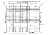
- FIG. 1 is a schematic diagram showing a configuration of a display device according to the present embodiment.
- FIG. 2 is a block diagram showing a configuration of the display device according to the present embodiment.
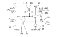
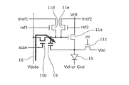
- FIG. 3 is a pixel circuit diagram of the display device according to the present embodiment.
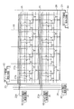
- FIG. 4 is a conceptual diagram showing the configuration of the display device according to the present embodiment.
- FIG. 5 is a diagram for explaining the operation of the display device according to the present embodiment.
- FIG. 6 is a timing chart showing the operation of the display device according to this embodiment.
- FIG. 7 is a diagram illustrating the operation of the pixel in the pre-initialization period.
- FIG. 8 is a diagram illustrating the operation of the pixel in the initialization period.
- FIG. 1 is a schematic diagram showing a configuration of a display device according to the present embodiment.
- FIG. 2 is a block diagram showing a configuration of the display device according to the present embodiment.
- FIG. 3 is a pixel circuit diagram of the display device according to
- FIG. 9 is a diagram illustrating the operation of the pixel during the Vth guarantee period.
- FIG. 10 is a diagram illustrating the operation of the pixel in the writing period.
- FIG. 11 is a diagram illustrating the operation of the pixel in the light emission period.
- FIG. 12 is a diagram for explaining the effect of the display device according to the present embodiment.
- FIG. 13 is a pixel circuit diagram of a display device according to the prior art.
- FIG. 14 is a diagram for explaining a display image by the display device according to the related art.
- FIG. 15 is an external view of a thin flat TV incorporating the display device according to the embodiment.
- FIG. 13 is a pixel circuit diagram of a display device according to the prior art.
- FIG. 14 is a diagram for explaining a display image by a display device according to the related art.
- the pixel of the display device includes a driving transistor 111a, switching transistors 111b, 111c, and 111d, an organic EL element 115, and a capacitive element 119.
- FIG. 14A is an operation transition diagram for explaining the progressive driving method of the organic EL light emitting panel.
- the horizontal axis represents time
- the vertical axis represents a pixel row (display row).
- the initialization operation, the Vth (threshold voltage) detection operation, the writing operation, and the light emitting operation are sequentially performed in a row in a display panel in which a plurality of pixels are arranged in a matrix. It is shown.
- the number of lines on the display panel is shown from the first line (1L) to the nth line (nL).
- n 2160 rows.
- the horizontal axis represents time
- the vertical axis represents the initialization voltage (Vref voltage).
- the first, second, and third fields on the horizontal axis indicate the first, second, and third fields of the displayed video.
- the pixel circuit is operated in the order of the conversion operation, the Vth detection operation, the writing operation, and the light emitting operation.
- a vertical blanking period is provided from the end of the writing period of the nth row of a certain frame to the start of the writing period of the first row of the next frame.
- virtual lines for example, 2161 to 2253 lines
- nLth line This corresponds to a vertical blanking period in which the gate driver secures a time for returning scanning from the last scanning line (second line 160) to the scanning start line (first line). This is represented by the number of scanning lines corresponding to the period.
- the vertical blanking period is a blanking period included in the video signal input from the outside, and is a period for returning scanning from the last line to the top line in the scanning of the video signal in the cathode ray tube.
- a vertical blanking period is technically unnecessary, but since such a period is included in the video signal, the display method is also supported in the video signal in the organic EL display device. Therefore, a vertical blanking period is provided.
- the initializing voltage fluctuates as shown in FIG. That is, when the panel is lit, the current load flowing through each power supply line varies due to the influence of the vertical blanking period and the display state, thereby varying the voltage ripple amount of each power supply line. For this reason, the electric charge charged to the capacitive element 119 fluctuates, and the problem that the work for which the blanking period is initialized becomes dark or bright, and the problem that dark lines and dark bands appear in the display image. There is.
- a display device in which a plurality of pixels are arranged in a matrix, and a current flows through each of the plurality of pixels.
- a light emitting element that emits light
- a capacitive element that accumulates electric charge according to the magnitude of a video signal applied to a data line
- a driving transistor that causes a current corresponding to the electric charge accumulated in the capacitive element to flow through the light emitting element
- a first switching transistor for pre-initializing the charge accumulated in the capacitive element, and a second for initializing the charge accumulated in the capacitive element after the pre-initialization.
- a first voltage source that outputs a first voltage to the capacitor when the first switching transistor is turned on; and When 2 of the switching transistor to the ON state, further comprising a second voltage source for applying a second voltage to the capacitive element.
- first voltage and the second voltage may be different values.
- the voltage applied to the capacitive element can be stabilized during the initialization period without being affected by the noise signal transmitted through the same voltage source.
- the first voltage may be larger than the second voltage.
- the display device driving method is a display device driving method in which a plurality of pixels is arranged in a matrix, and is stored in a capacitor provided in each of the plurality of pixels.
- a pre-initializing step for initializing the charged electric charge, an initializing step for re-initializing the electric charge accumulated in the capacitor element after the pre-initializing step, and a driving device provided in each of the plurality of pixels
- a threshold voltage detecting step for detecting a threshold voltage of the transistor
- a writing step for storing a charge corresponding to a magnitude of a video signal in the capacitor; and a current corresponding to the amount of the charge stored in the capacitor.
- a light emitting step of causing the light emitting element to emit light.
- the first voltage is applied from the first voltage source to the capacitor element by turning on the first switching transistor, and in the second initialization step, the first voltage is applied.
- the second voltage may be applied to the capacitor element from the second voltage source by turning on the second switching transistor.
- first voltage and the second voltage may be different values.
- the voltage applied to the capacitive element can be stabilized during the initialization period without being affected by the noise signal transmitted through the same voltage source.
- the first voltage may be larger than the second voltage.
- FIG. 1 is a schematic diagram showing a configuration of a display device according to the present embodiment.
- FIG. 2 is a block diagram showing a configuration of the display device according to the present embodiment.
- FIG. 3 is a circuit diagram of the pixel 16 of the display device according to the present embodiment.
- the display device includes a display screen 20, a COF (Chip On Film) 34, gate printed boards 35 a and 35 b, and a source printed board 36. Yes.
- COF Chip On Film
- a circuit 31 constituting a gate driver or a circuit 32 constituting a source driver is arranged in the COF 34.
- the COF 34 in which the circuit 31 is disposed is disposed so as to connect the display screen 20 and the gate printed circuit board 35a or 35b.
- the COF 34 in which the circuit 32 is disposed is disposed so as to connect the display screen 20 and the source printed board 36.
- the COF 34 is connected to the display screen 20, the gate printed boards 35a and 35b, and the source printed board 36 with an ACF (Anisotropic Conductive Film) resin.
- ACF Anaisotropic Conductive Film
- a plurality of circuits 31 arranged between the display screen 20 and the gate printed board 35a are collectively referred to as a gate driver circuit 12a.
- the plurality of circuits 31 arranged between the display screen 20 and the gate printed board 35b are collectively referred to as a gate driver circuit 12b.
- a plurality of circuits 32 arranged between the display screen 20 and the source printed circuit board 36 are collectively referred to as a source driver circuit 14.
- the gate driver circuits 12 a and 12 b are connected to the scanning line 17.
- the gate driver circuits 12a and 12b apply a control voltage to the scanning line 17 to turn on or off switching transistors 11b to 11e disposed in the pixel 16 described later.
- the source driver circuit 14 is connected to the data line 18 and applies a video signal to the data line 18.
- a plurality of pixels 16 are arranged in a matrix on the display screen 20. As shown in FIG. 2, the pixel 16 is connected to a scanning line 17 electrically connected to the gate driver circuit 12 a or 12 b and a data line 18 electrically connected to the source driver circuit 14. .
- the pixel 16 includes an organic EL element 15, a driving transistor 11a, switching transistors 11b to 11e, and a capacitive element 19. Further, the pixel 16 includes a reference power supply line 22a (Vref1), a reference power supply line 22b (Vref2), an EL anode power supply line 23 (Vtft), an EL cathode power supply line 24 (Vel), and an initialization power supply line 25 ( Vini), the scanning line 17 (scan), the reference voltage control line 27a (ref1) and the reference voltage control line 27b (ref2), the initialization control line 28 (ini), and the data line 18 (Vdata) are wired.
- a reference power supply line 22a Vref1
- Vref2 a reference power supply line 22b
- Vtft EL anode power supply line 23
- Vel EL cathode power supply line 24
- Vini initialization power supply line 25
- FIG. 4 is a conceptual diagram showing the configuration of the display device according to the present embodiment.
- the display device includes an anode voltage generation circuit 42, a cathode voltage generation circuit 44, a Vini voltage generation circuit 46, a Vref1 voltage generation circuit 48, and a Vref2 voltage generation circuit 50.
- the anode voltage generation circuit 42 is connected to the EL anode power supply line 23 (Vtft) and generates an anode voltage to be applied to the organic EL element 15.
- the cathode voltage generation circuit 44 is connected to the EL cathode power supply line 24 (Vel) and generates a cathode voltage to be applied to the organic EL element 15. Note that the EL cathode power supply line 24 (Vel) may be grounded instead of being connected to the cathode voltage generation circuit 44.
- the Vini voltage generation circuit 46 is connected to the initialization power supply line 25 (Vini), and generates an initialization voltage Vini for initializing the capacitive element 19.
- the Vref1 voltage generation circuit 48 generates an initialization voltage Vref1 for initializing the capacitive element 19.
- the Vref2 voltage generation circuit 50 generates an initialization voltage Vref2 for pre-initializing the capacitive element 19.
- the switching transistors 11e and 11d correspond to a first transistor and a second transistor according to the present disclosure, respectively.
- the Vref2 voltage generation circuit 50 and the Vref1 voltage generation circuit 48 correspond to a first voltage source and a second voltage source according to the present disclosure, respectively.
- the voltage Vref2 and the voltage Vref1 correspond to the first voltage and the second voltage according to the present disclosure, respectively.
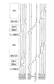
- FIG. 5 is a diagram for explaining the operation of the display device according to the present embodiment.
- FIG. 6 is a timing chart showing the operation of the display device according to this embodiment.
- the display device when the display device according to the present embodiment displays an image on a display, a pre-initialization operation, an initialization operation, a threshold voltage (Vth) detection operation for one row (1L), The operation is performed in the order of the writing operation and the light emitting operation.
- Vth threshold voltage
- the horizontal axis represents time
- the vertical axis represents the reference voltage control line 27b (ref2)
- the reference voltage control line 27a (ref1) represents the initialization control line 28 (ini)
- the scanning line 17 (scan) in the pixels 16 of each row.
- the voltage signal applied to is shown.
- a series of operations including a pre-initialization operation, an initialization operation, a threshold voltage (Vth) detection operation, a write operation, and a light emission operation are performed in order from the first row to the last row n. Done.
- a high level voltage is applied to the reference voltage control line 27b (ref2).
- a low level voltage is applied to the reference voltage control line 27b (ref2), and a high level voltage is applied to the reference voltage control line 27a (ref1) and the initialization control line 28 (ini).
- a low level voltage is applied to the initialization control line 28 (ini).
- a low level voltage is applied to the reference voltage control line 27b (ref2), the reference voltage control line 27a (ref1), and the initialization control line 28 (ini), and a high level is applied to the scanning line 17 (scan). Is applied.
- pre-initialization operation and the initialization operation correspond to a first initialization process and a second initialization process in the present disclosure, respectively.
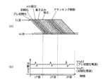
- FIG. 12 is a diagram for explaining the effect of the display device according to the present embodiment, and FIG. 12A shows an operation state (display video) of a certain column of pixels in time series. (B) of the figure shows the voltage Vref in a pixel in the same column as shown in (a).
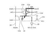
- FIG. 7 is a diagram illustrating the operation of the pixel 16 in the pre-initialization period.
- the pre-initialization period is a period provided prior to the initialization period, and is a period provided for applying a stable voltage to the capacitor element 19 when charging the capacitor element 19 in the initialization period. .
- the voltage applied to the capacitor 19 is more stabilized in the initialization period that is performed subsequent to the pixel in the row that is initialized during the blanking period. Can do.
- the voltage Vref2 is applied to the first electrode of the capacitive element 19 and the gate of the driving transistor 11a. Specifically, the voltage level of the reference voltage control line 27b is changed from Low to High, and the switching transistor 11e is turned on. Thereby, as shown in FIG. 7, the voltage Vref2 is charged from the Vref2 voltage generation circuit 50 to the capacitive element 19 through the reference power supply line 22b. The voltage waveform of the voltage Vref2 at this time will be described later.
- the voltage Vref2 may be output from the Vref2 voltage generation circuit 50 that is a voltage source, or if it is not the same as the Vref1 voltage generation circuit 48 that is a voltage source that generates the voltage Vref1, the anode voltage generation circuit 42, the cathode The voltage generation circuit 44 and the Vini voltage generation circuit 46 may be shared.
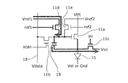
- FIG. 8 is a diagram illustrating the operation of the pixel 16 in the initialization period.
- the initialization period is a period during which the capacitance element 19 is charged with a voltage necessary for flowing a drain current in the Vth detection period of the driving transistor 11a.
- the initialization period first, a high level voltage is applied to the initialization control line 28 (ini), and only the switch transistor 11c is turned on (on state). As a result, the source potential of the driving transistor 11a is set to the voltage Vini, and the source potential of the driving transistor 11a is stabilized.
- a voltage necessary for flowing the drain current to detect the threshold voltage of the driving transistor 11a in the subsequent Vth detection period is applied in advance to the first electrode of the capacitor 19 and the gate of the driving transistor 11a.
- the voltage level of the reference voltage control line 27a is changed from Low to High, and the switching transistor 11d is turned on.
- the voltage Vref1 is charged to the capacitive element 19 from the Vref1 voltage generation circuit 48 via the reference power supply line 22a.
- Vref1 and Vref2 may be different sizes.
- the magnitude of Vref2 may be larger than Vref1.
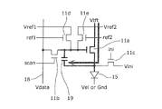
- FIG. 9 is a diagram illustrating the operation of the pixel 16 during the Vth detection period.
- the Vth detection period is a period in which the threshold voltage of the driving transistor 11a is detected by the capacitive element 19.
- the threshold voltage of the driving transistor 11a is detected by the capacitive element 19. Specifically, the voltage of the scanning line 17 and the initialization control line 28 is maintained at the low level, and the voltage of the reference voltage control line 27a is maintained at the high level. That is, the switching transistors 11b and 11c are turned off, and the switching transistor 11d is turned on.
- the drain current flows through the driving transistor 11a without current flowing through the organic EL element 15, and the source potential of the driving transistor 11a changes. .
- the source potential of the driving transistor 11a changes until the drain current supplied by the voltage Vtft of the EL anode power supply line 23 becomes zero.
- the threshold voltage detection operation of the driving transistor 11a is started.
- the potential difference (the gate-source voltage of the driving transistor 11a) between the first electrode and the second electrode of the capacitive element 19 (the electrode connected to the anode of the organic EL element 15) is The potential difference corresponds to the threshold voltage Vth of the driving transistor 11a. Thereafter, a low level voltage is applied to the reference voltage control line 27a, whereby the switching transistor 11d is turned off. Thereby, the supply of the drain current of the driving transistor 11a is stopped, and the threshold voltage detection operation is completed.
- a low level voltage is applied to the reference voltage control line 27a to turn off the switching transistor 11d. Specifically, the voltage of the reference voltage control line 27a is changed from the High level to the Low level while maintaining the voltages of the initialization control line 28 and the scanning line 17 at the Low level.
- the data signal voltage supplied to the data line 18 and the voltage Vref1 of the reference power supply line 22a are simultaneously applied to the first electrode of the capacitive element 19 (the electrode on the side where the organic EL element 15 is not connected). Can be prevented.
- FIG. 10 is a diagram illustrating the operation of the pixel 16 in the writing period.
- the writing period is a period in which a video signal voltage (data signal voltage) corresponding to the display gradation is taken into the pixel 16 from the data line 18 and written into the capacitor 19 of the pixel 16.
- the switching transistor 11b is first turned on for a predetermined period to prepare for the writing operation. Specifically, the voltage of the scanning line 17 is changed from the low level to the high level. At this time, the switching transistors 11c, 11d, and 11e and the driving transistor 11a are off.
- a video signal voltage (data signal voltage) corresponding to the display gradation is taken into the pixel 16 from the data line 18 and written into the capacitor 19.
- the data signal voltage is applied to the first electrode of the capacitive element 19 through the data line 18 and the switching transistor 11b.
- the capacitor 19 has a voltage difference between the data signal voltage and the voltage Vref (parasitic capacitance of the organic EL element 15) / It is multiplied (parasitic capacitance of the organic EL element 15 + capacitance of the capacitive element 19) and stored (held).
- FIG. 11 is a diagram illustrating the operation of the pixel 16 during the light emission period.
- the light emission period is a period in which the organic EL element 15 emits light at a display gradation corresponding to the magnitude of the video signal voltage (data signal voltage) written in the capacitor element 19.
- the voltages of the scanning line 17, the reference voltage control line 27a, and the initialization control line 28 are maintained at a low level. That is, the switching transistors 11b, 11d, and 11c are kept off.
- a voltage corresponding to the electric charge stored in the capacitive element 19 is applied to the gate of the driving transistor 11a, and the driving transistor 11a is turned on. Then, as shown in FIG. 11, a current corresponding to the magnitude of the electric charge stored in the capacitive element 19 is supplied to the organic EL element 15 via the EL anode power line 23 (Vtft). Thereby, the organic EL element 15 emits light according to the magnitude of the electric charge stored in the capacitive element 19.
- FIG. 12 is a diagram for explaining the effect of the display device according to the present embodiment, and FIG. 12A shows an operation state (display video) of a certain column of pixels in time series. (B) of the figure shows the voltage Vref in a pixel in the same column as shown in (a).
- FIG. 12A is an operation
- the horizontal axis represents time
- the vertical axis represents a pixel row (display row).
- pre-initialization operation, initialization operation, Vth (threshold voltage) detection operation, write operation, and light emission operation are sequentially executed in a row in a display panel in which a plurality of pixels are arranged in a matrix. It has been shown that.
- the number of lines on the display panel is shown from the first line (1L) to the nth line (nL).
- n 2160 rows.
- the horizontal axis represents time
- the vertical axis represents the initialization voltage (Vref voltage).
- the first, second, and third fields on the horizontal axis indicate the first, second, and third fields of the displayed video.
- virtual lines for example, 2161 to 2253 lines
- nLth line This corresponds to a vertical blanking period in which the gate driver secures a time for returning scanning from the last scanning line (second line 160) to the scanning start line (first line). This is represented by the number of scanning lines corresponding to the period.
- FIG. 12B shows a voltage Vref2 in the pre-initialization operation and a voltage Vref1 in the initialization operation.
- the voltage Vref2 varies as shown in the figure, but the voltage Vref1 does not vary. Therefore, by providing a pre-initialization operation before the initialization operation, it is possible to eliminate fluctuations in the initialization voltage and display a video signal having no output deviation.
- the method for driving the display device by providing the pre-initialization operation before the initialization operation, the variation in the initialization voltage is eliminated and the video signal without output deviation is displayed. be able to.
- the display device is not limited to the above-described embodiment.
- the present invention includes modifications obtained by making various modifications conceived by those skilled in the art within the scope of the present invention without departing from the gist of the present invention, and various devices incorporating a display device.
- the circuit configuration of the pixel 16 is not limited to the circuit configuration described above.
- the configuration in which the driving transistor 11a and the organic EL element 15 are arranged in this order between the EL anode power supply line 23 and the EL cathode power supply line 24 is exemplified.
- a switch transistor may be further provided between the transistor 23 and the driving transistor 11a. Thereby, a current can be stably passed through the organic EL element 15 by turning the switch transistor on or off.
- the anode voltage generation circuit 42, the driving transistor 11a, and the switching transistor may be arranged in this order, or these three elements may be arranged in a different order. That is, in the display device of the present invention, regardless of whether the driving transistor is n-type or p-type, the drain electrode and the source electrode of the driving transistor 11a, and the anode electrode and the cathode electrode of the organic EL element 15 are The arrangement order of the driving transistor 11 a and the organic EL element 15 is not limited as long as it is arranged on the current path between the EL anode power supply line 23 and the EL cathode power supply line 24.
- the circuit configuration of the pixel 16 is not limited to the circuit configuration described above.
- a switching transistor may be provided between the EL anode power supply line 23 and the EL cathode power supply line 24.
- the switching transistor, the driving transistor 11a, and the organic EL element 15 may be arranged in this order.
- the three elements of the switching transistor, the driving transistor 11a, and the organic EL element 15 may be arranged in a different order.
- the drain electrode and the source electrode of the driving transistor 11a and the anode electrode and the cathode electrode of the organic EL element 15 are The arrangement order of the driving transistor 11 a and the organic EL element 15 is not limited as long as it is arranged on the current path between the EL anode power supply line 23 and the EL cathode power supply line 24.
- the switching transistors 11b to 11e have been described on the premise that they are MOSFETs having a gate electrode, a source electrode, and a drain electrode. However, these transistors include a base, a collector, and an emitter. A bipolar transistor may be applied. Also in this case, the object of the present invention is achieved and the same effect is produced.
- control circuit and the arithmetic circuit included in the display device according to the above-described embodiment are typically realized as an LSI that is an integrated circuit.
- a part of the control circuit and the arithmetic circuit included in the display device described above can be integrated on the same substrate as the display screen 20.
- an FPGA Field Programmable Gate Array
- a reconfigurable processor that can reconfigure the connection and setting of the circuit cells inside the LSI may be used.
- some of the functions of the scan line driver circuit, the data line driver circuit, the control circuit, and the arithmetic circuit included in the display device according to the embodiment may be realized by a processor such as a CPU executing a program. Good.
- the display device uses an organic EL element
- the display device may be applied to a display device using a light emitting element other than the organic EL element.
- the display device according to the embodiment is built in a thin flat TV as shown in FIG.
- a thin flat TV capable of displaying images with high accuracy with reduced display unevenness is realized.
- the present invention is particularly useful for an active organic EL flat panel display.
Landscapes
- Engineering & Computer Science (AREA)
- Physics & Mathematics (AREA)
- Computer Hardware Design (AREA)
- General Physics & Mathematics (AREA)
- Theoretical Computer Science (AREA)
- Control Of Indicators Other Than Cathode Ray Tubes (AREA)
- Control Of El Displays (AREA)
Abstract
Description
本発明者は、「背景技術」の欄において記載したアクティブマトリクス型の有機ELディスプレイに関し、以下の問題が生じることを見出した。以下、本問題について説明する。
以下、適宜図面を参照しながら、実施の形態を詳細に説明する。但し、必要以上に詳細な説明は省略する場合がある。例えば、既によく知られた事項の詳細説明や実質的に同一の構成に対する重複説明を省略する場合がある。これは、以下の説明が不必要に冗長になるのを避け、当業者の理解を容易にするためである。
図1は、本実施の形態に係る表示装置の構成を示す概略図である。図2は、本実施の形態にかかる表示装置の構成を示すブロック図である。図3は、本実施の形態にかかる表示装置の画素16の回路図である。
次に、表示装置の駆動方法について説明する。図5は、本実施の形態にかかる表示装置の動作について説明するための図である。図6は、本実施の形態にかかる表示装置の動作を示すタイミングチャートである。
はじめに、プレ初期化期間について説明する。図7は、プレ初期化期間における画素16の動作を示す図である。
次に、初期化期間について説明する。図8は、初期化期間における画素16の動作を示す図である。
次に、Vth検出期間について説明する。図9は、Vth検出期間における画素16の動作を示す図である。
次に、書き込み期間について説明する。図10は、書き込み期間における画素16の動作を示す図である。
次に、発光期間について説明する。図11は、発光期間における画素16の動作を示す図である。
図12は、本実施の形態にかかる表示装置の効果を説明するための図であり、図12の(a)は、ある1列の画素の動作状態(表示映像)を時系列に沿って示す図、同図の(b)は、(a)に示したのと同一の列のある画素における電圧Vrefを示す図である。
以上、実施の形態に係る表示装置について説明したが、表示装置は、上述した実施の形態に限定されるものではない。上述した実施の形態に対して、本発明の主旨を逸脱しない範囲で当業者が思いつく各種変形を施して得られる変形例や、表示装置を内蔵した各種機器も本発明に含まれる。
11b、11c、111b、111c スイッチ用トランジスタ
11d、111d スイッチ用トランジスタ(第2のスイッチ用トランジスタ)
11e スイッチ用トランジスタ(第1のスイッチ用トランジスタ)
12a、12b ゲートドライバ回路
14 ソースドライバ回路
15、115 有機EL素子(発光素子)
16 画素
17 走査線
18 データ線
19、119 容量素子
20 表示画面
22a、22b 参照電源線
23 ELアノード電源線
24 ELカソード電源線
25 初期化電源線
27a、27b 参照電圧制御線
28 初期化制御線
31、32 回路
34 COF
35a、35b ゲートプリント基板
36 ソースプリント基板
42 アノード電圧発生回路
44 カソード電圧発生回路
46 Vini電圧発生回路
48 Vref1電圧発生回路(第2の電圧源)
50 Vref2電圧発生回路(第1の電圧源)
Claims (7)
- 複数の画素がマトリクス状に配置された表示装置であって、
前記複数の画素のそれぞれは、
電流が流れることにより発光する発光素子と、
データ線に印加される映像信号の大きさに応じた電荷を蓄積する容量素子と、
前記容量素子に蓄積された電荷に応じた電流を前記発光素子に流す駆動用トランジスタと、
前記容量素子に蓄積された電荷をプレ初期化するための第1のスイッチ用トランジスタと、
前記プレ初期化の後、さらに、前記容量素子に蓄積された電荷を初期化するための第2のスイッチ用トランジスタと、を備え、
前記表示装置は、
前記第1のスイッチ用トランジスタをオン状態としたときに、前記容量素子に第1の電圧を出力する第1の電圧源と、
前記第2のスイッチ用トランジスタをオン状態としたときに、前記容量素子に第2の電圧を印加する第2の電圧源と、をさらに備える
表示装置。 - 前記第1の電圧と前記第2の電圧とは異なる値である
請求項1に記載の表示装置。 - 前記第1の電圧は、前記第2の電圧より大きい
請求項2に記載の表示装置。 - 複数の画素がマトリクス状に配置された表示装置の駆動方法であって、
前記複数の画素のそれぞれに設けられた容量素子に蓄積された電荷を初期化するプレ初期化工程と、
前記プレ初期化工程の後に、前記容量素子に蓄積された電荷を再度初期化する初期化工程と、
前記複数の画素のそれぞれに設けられた駆動用トランジスタの閾値電圧を検出する閾値電圧検出工程と、
前記容量素子に、映像信号の大きさに対応した電荷を蓄積する書き込み工程と、
前記容量素子に蓄積された電荷量に応じた電流を発光素子に流して前記発光素子を発光させる発光工程と、を含む
表示装置の駆動方法。 - 前記プレ初期化工程において、第1のスイッチ用トランジスタをオン状態とすることにより、第1の電圧源から前記容量素子に第1の電圧が印加され、
第2の初期化工程において、第2のスイッチ用トランジスタをオン状態とすることにより、第2の電圧源から前記容量素子に第2の電圧が印加される
請求項4に記載の表示装置の駆動方法。 - 前記第1の電圧と前記第2の電圧とは異なる値である
請求項5に記載の表示装置の駆動方法。 - 前記第1の電圧は、前記第2の電圧より大きい
請求項6に記載の表示装置の駆動方法。
Priority Applications (2)
| Application Number | Priority Date | Filing Date | Title |
|---|---|---|---|
| JP2015560866A JPWO2015118599A1 (ja) | 2014-02-10 | 2014-12-22 | 表示装置および表示装置の駆動方法 |
| US15/117,235 US20160351120A1 (en) | 2014-02-10 | 2014-12-22 | Display device and method for driving display device |
Applications Claiming Priority (2)
| Application Number | Priority Date | Filing Date | Title |
|---|---|---|---|
| JP2014-023820 | 2014-02-10 | ||
| JP2014023820 | 2014-02-10 |
Publications (1)
| Publication Number | Publication Date |
|---|---|
| WO2015118599A1 true WO2015118599A1 (ja) | 2015-08-13 |
Family
ID=53777440
Family Applications (1)
| Application Number | Title | Priority Date | Filing Date |
|---|---|---|---|
| PCT/JP2014/006401 Ceased WO2015118599A1 (ja) | 2014-02-10 | 2014-12-22 | 表示装置および表示装置の駆動方法 |
Country Status (3)
| Country | Link |
|---|---|
| US (1) | US20160351120A1 (ja) |
| JP (1) | JPWO2015118599A1 (ja) |
| WO (1) | WO2015118599A1 (ja) |
Cited By (1)
| Publication number | Priority date | Publication date | Assignee | Title |
|---|---|---|---|---|
| JP2016009135A (ja) * | 2014-06-25 | 2016-01-18 | 株式会社Joled | 表示装置及びその駆動方法 |
Families Citing this family (5)
| Publication number | Priority date | Publication date | Assignee | Title |
|---|---|---|---|---|
| KR102218779B1 (ko) * | 2014-07-04 | 2021-02-19 | 엘지디스플레이 주식회사 | Oled 표시 장치 |
| CN104773594B (zh) * | 2015-03-23 | 2017-01-11 | 京东方科技集团股份有限公司 | 一种覆晶薄膜贴附装置 |
| CN104680980B (zh) * | 2015-03-25 | 2017-02-15 | 京东方科技集团股份有限公司 | 像素驱动电路及其驱动方法、显示装置 |
| KR102888503B1 (ko) * | 2019-08-05 | 2025-11-20 | 삼성디스플레이 주식회사 | 표시 장치 |
| CN111583865B (zh) * | 2020-06-12 | 2021-11-26 | 京东方科技集团股份有限公司 | 显示面板、显示装置及开关器件的沟道宽长比的确定方法 |
Citations (2)
| Publication number | Priority date | Publication date | Assignee | Title |
|---|---|---|---|---|
| JP2009047958A (ja) * | 2007-08-21 | 2009-03-05 | Sony Corp | 有機エレクトロルミネッセンス発光部の駆動方法、及び、有機エレクトロルミネッセンス表示装置 |
| JP2010266848A (ja) * | 2009-04-17 | 2010-11-25 | Toshiba Mobile Display Co Ltd | El表示装置及びその駆動方法 |
Family Cites Families (3)
| Publication number | Priority date | Publication date | Assignee | Title |
|---|---|---|---|---|
| KR100739334B1 (ko) * | 2006-08-08 | 2007-07-12 | 삼성에스디아이 주식회사 | 화소와 이를 이용한 유기전계발광 표시장치 및 그의구동방법 |
| US20110015713A1 (en) * | 2008-10-23 | 2011-01-20 | Pacesetter, Inc. | Systems and methods for reducing lead heating and the risks of mri-induced stimulation |
| KR101329964B1 (ko) * | 2009-12-31 | 2013-11-13 | 엘지디스플레이 주식회사 | 유기 발광 다이오드 표시 장치 |
-
2014
- 2014-12-22 US US15/117,235 patent/US20160351120A1/en not_active Abandoned
- 2014-12-22 WO PCT/JP2014/006401 patent/WO2015118599A1/ja not_active Ceased
- 2014-12-22 JP JP2015560866A patent/JPWO2015118599A1/ja active Pending
Patent Citations (2)
| Publication number | Priority date | Publication date | Assignee | Title |
|---|---|---|---|---|
| JP2009047958A (ja) * | 2007-08-21 | 2009-03-05 | Sony Corp | 有機エレクトロルミネッセンス発光部の駆動方法、及び、有機エレクトロルミネッセンス表示装置 |
| JP2010266848A (ja) * | 2009-04-17 | 2010-11-25 | Toshiba Mobile Display Co Ltd | El表示装置及びその駆動方法 |
Cited By (1)
| Publication number | Priority date | Publication date | Assignee | Title |
|---|---|---|---|---|
| JP2016009135A (ja) * | 2014-06-25 | 2016-01-18 | 株式会社Joled | 表示装置及びその駆動方法 |
Also Published As
| Publication number | Publication date |
|---|---|
| US20160351120A1 (en) | 2016-12-01 |
| JPWO2015118599A1 (ja) | 2017-03-23 |
Similar Documents
| Publication | Publication Date | Title |
|---|---|---|
| JP6142178B2 (ja) | 表示装置および駆動方法 | |
| CN102388414B (zh) | 显示装置及其驱动方法 | |
| US9591715B2 (en) | OLED driving compensation circuit and driving method thereof | |
| CN104575398B (zh) | 像素电路及其驱动方法、显示装置 | |
| CN104464643B (zh) | 显示装置、像素驱动电路及其驱动方法 | |
| US9852685B2 (en) | Pixel circuit and driving method thereof, display apparatus | |
| US20160210906A1 (en) | Organic light-emitting display apparatus | |
| JP5756865B2 (ja) | 表示装置及びその制御方法 | |
| US20140049169A1 (en) | Active matrix organic light emitting diode circuit and operating method of the same | |
| CN104700782B (zh) | Oeld像素电路、显示装置及控制方法 | |
| JP6288710B2 (ja) | 表示装置の駆動方法および表示装置 | |
| US20170352316A1 (en) | Pixel circuit and drive method therefor, and active matrix organic light-emitting display | |
| JP6175718B2 (ja) | 駆動方法および表示装置 | |
| CN104751777A (zh) | 像素电路、像素及包括该像素的amoled显示装置及其驱动方法 | |
| CN108877649B (zh) | 像素电路及其驱动方法、显示面板 | |
| WO2015118599A1 (ja) | 表示装置および表示装置の駆動方法 | |
| JP2014215425A (ja) | 表示装置および表示装置の駆動方法 | |
| WO2015132834A1 (ja) | 有機el表示装置 | |
| JP2016099505A (ja) | 表示装置 | |
| JP2010066331A (ja) | 表示装置 | |
| JP6196809B2 (ja) | 画素回路及びその駆動方法 | |
| CN109192139B (zh) | 一种像素补偿电路 | |
| JP6312083B2 (ja) | 表示装置及びその駆動方法 | |
| JP2016048300A (ja) | 表示装置の駆動方法及び表示装置 | |
| CN204614415U (zh) | 有机发光二极管像素电路及显示装置 |
Legal Events
| Date | Code | Title | Description |
|---|---|---|---|
| 121 | Ep: the epo has been informed by wipo that ep was designated in this application |
Ref document number: 14881746 Country of ref document: EP Kind code of ref document: A1 |
|
| ENP | Entry into the national phase |
Ref document number: 2015560866 Country of ref document: JP Kind code of ref document: A |
|
| WWE | Wipo information: entry into national phase |
Ref document number: 15117235 Country of ref document: US |
|
| NENP | Non-entry into the national phase |
Ref country code: DE |
|
| 122 | Ep: pct application non-entry in european phase |
Ref document number: 14881746 Country of ref document: EP Kind code of ref document: A1 |