WO2015114944A1 - サイドチャネル攻撃の検知装置、サイドチャネル攻撃の検知装置によるサイドチャネル攻撃の検知方法 - Google Patents
サイドチャネル攻撃の検知装置、サイドチャネル攻撃の検知装置によるサイドチャネル攻撃の検知方法 Download PDFInfo
- Publication number
- WO2015114944A1 WO2015114944A1 PCT/JP2014/082010 JP2014082010W WO2015114944A1 WO 2015114944 A1 WO2015114944 A1 WO 2015114944A1 JP 2014082010 W JP2014082010 W JP 2014082010W WO 2015114944 A1 WO2015114944 A1 WO 2015114944A1
- Authority
- WO
- WIPO (PCT)
- Prior art keywords
- side channel
- channel attack
- oscillator
- circuit
- detection device
- Prior art date
- Legal status (The legal status is an assumption and is not a legal conclusion. Google has not performed a legal analysis and makes no representation as to the accuracy of the status listed.)
- Ceased
Links
Images









Classifications
-
- H—ELECTRICITY
- H04—ELECTRIC COMMUNICATION TECHNIQUE
- H04L—TRANSMISSION OF DIGITAL INFORMATION, e.g. TELEGRAPHIC COMMUNICATION
- H04L9/00—Cryptographic mechanisms or cryptographic arrangements for secret or secure communications; Network security protocols
- H04L9/10—Cryptographic mechanisms or cryptographic arrangements for secret or secure communications; Network security protocols with particular housing, physical features or manual controls
-
- H—ELECTRICITY
- H04—ELECTRIC COMMUNICATION TECHNIQUE
- H04L—TRANSMISSION OF DIGITAL INFORMATION, e.g. TELEGRAPHIC COMMUNICATION
- H04L9/00—Cryptographic mechanisms or cryptographic arrangements for secret or secure communications; Network security protocols
- H04L9/002—Countermeasures against attacks on cryptographic mechanisms
Definitions
- the present invention relates to a side channel attack detection device and a side channel attack detection method using a side channel attack detection device, and more particularly to a countermeasure technique for side channel attacks against information processing devices such as cryptographic LSIs in the field of cryptographic engineering.
- Cryptography is a fundamental technology that is indispensable for building such a social system, and large-scale integrated circuits (hereinafter referred to as cryptographic LSIs) that operate software and hardware that implement cryptographic algorithms are used in many consumer products. It is mounted on.
- cryptographic LSI a cryptographic algorithm that has been sufficiently evaluated for safety by an expert is usually used. For this reason, there is little concern about leakage of pre-encrypted data (plaintext) or secret key due to algorithmic defects (in terms of current computational capabilities and known decryption methods).
- the electromagnetic wave analysis attack enables a non-contact attack compared to the power analysis that directly probes the device and measures the transient voltage change of the entire LSI.
- local characteristics of a cryptographic LSI can be obtained, and it has been pointed out that it may pose a threat to devices that have been considered difficult to apply power analysis.
- the secret information can be obtained in principle from the local electromagnetic radiation of the part that processes the secret information due to the asymmetry of the minimum components (basic gates such as AND and XOR) of general cryptographic LSI. (For example, refer nonpatent literature 1).
- Non-Patent Document 2 Wive Dynamic Differential Logic
- this measure increases the circuit scale at least several times.
- Non-Patent Document 3 As a countermeasure at the analog circuit level, a power supply current equalizer (see, for example, Non-Patent Document 3) that equalizes the power consumption of the cryptographic LSI regardless of the internal operation state has also been proposed. It is effective for power analysis attacks, but still cannot cope with side channel attacks described in Non-Patent Document 1.
- the present invention is an example of a problem to deal with such a problem. That is, it aims at providing the detection apparatus which can detect a side channel attack with a simple structure, the detection method of a side channel attack, etc.
- a side-channel attack detection apparatus includes an inductor disposed in proximity to an information processing apparatus that is a target of a side-channel attack, and changes the inductance of the inductor. And detecting means for detecting, and determining means for determining approach of the probe or opening of the LSI package by the side channel attack based on an output of the detecting means.
- a detection apparatus for a side channel attack includes a capacitor disposed in proximity to an information processing apparatus that is a target of a side channel attack, and a detection unit that detects a change in capacitance of the capacitor, Determining means for determining approach of the probe or opening of the LSI package due to the side channel attack based on an output of the detecting means.
- the side channel attack detection method of the present invention is performed using the side channel attack detection apparatus according to the present invention.
- the present invention it is possible to provide a detection device capable of detecting a side channel attack with a simple structure. Further, according to the present invention, it is possible to provide a side channel attack detection method capable of easily detecting a side channel attack by using a detection device.
- the flowchart which shows an example of the detection method of the side channel attack using the detection apparatus of the side channel attack which concerns on embodiment of this invention.
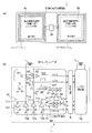
- the figure which shows an example of the detection apparatus which concerns on embodiment of this invention (a) is a conceptual diagram of a detection apparatus, (b) is a circuit diagram which shows a specific example of the detection apparatus shown to (a).
- a timing chart showing an example of the operation of the detection device and the information processing device (encryption processing circuit) (a) is a diagram showing an example of the operation of the encryption processing circuit, (b) is a diagram showing an example of a signal related to the LC oscillation circuit, (C) is a figure which shows an example of the signal regarding a ring oscillation circuit.
- the figure which shows an example of a frequency spectrum (a) is the case of 3 winding coil L2 (no probe approach), (b) is the case of 4 winding coil L1 (no probe approach), (c) is the case of 3 winding coil L2 (There is a probe approach in L1), (d) is the case of the 4-turn coil L1 (a probe approach is in L1).
- movement by the detection of a side channel attack, (a), (b) is a figure which respectively shows an example of the waveform of an electromagnetic wave in the case of no operation switching by attack detection, and an example of a correlation coefficient.
- (c), (d) is a diagram showing an example of an electromagnetic wave waveform and an example of a correlation coefficient when there is an operation switching by attack detection.
- the conceptual diagram for demonstrating an example of the detection apparatus of the side channel attack which concerns on other embodiment of this invention.
- the figure which shows an example of a transfer function (a) is a figure which shows an example of a transfer function when a probe is not approaching a detection means, (b) is an example of a transfer function when a probe is approaching to a detection means FIG.
- the detection device detects the side channel attack itself.
- the side channel attack detection apparatus includes an inductor or a capacitor disposed in proximity to an information processing apparatus that is a target of the side channel attack, and an inductance of the inductor (coil) or a capacitance of the capacitor.
- the detection device can detect a change in inductance or capacitance, such as when a probe is approaching or an LSI package is opened, by a detection unit, and can easily determine a side channel attack by a determination unit.
- the detection device can detect a side channel attack based on the electromagnetic laws of electromagnetics, and when such an attack is detected, a secret encryption is performed by performing processing such as stopping / changing the subsequent cryptographic processing. Prevent information leakage.
- the detection device for example, side channel attack (secondary information generated during the operation of the encryption LSI) against the encryption LSI (a large-scale integrated circuit on which software or hardware realizing the encryption algorithm operates) as an information processing device. (Attack for stealing secret information by observing (side channel information)).
- side channel attack secondary information generated during the operation of the encryption LSI
- the encryption LSI a large-scale integrated circuit on which software or hardware realizing the encryption algorithm operates
- the detection apparatus changes the inductance caused by the probe.
- the electromagnetic field changes in the nearby electromagnetic field of information processing devices, changes in characteristic impedance inside the circuit, changes in electrical parameters such as the occurrence of signal loss flowing inside the circuit
- local electromagnetic wave analysis Prevent all side-channel attacks that use electrical information from probing, including attacks. Since the change in the electrical parameter is caused by electric field coupling, magnetic field coupling, or both of the probe and the cryptographic LSI, it is theoretically difficult to execute an attack involving probing while avoiding these.
- the attack detection sensor portion (detection means) of the detection device according to the embodiment of the present invention can be realized by a simple circuit such as an LC oscillator including an inductor (coil), as described later, Even if it is included, it can be realized with an area overhead of only a few percent with respect to a cryptographic LSI (information processing apparatus) as a countermeasure target.
- a simple circuit such as an LC oscillator including an inductor (coil), as described later, Even if it is included, it can be realized with an area overhead of only a few percent with respect to a cryptographic LSI (information processing apparatus) as a countermeasure target.
- FIG. 1 is a flowchart showing an example of a side channel attack detection method using the side channel attack detection apparatus according to the embodiment of the present invention.
- FIG. 2 is a diagram illustrating an example of a side channel attack detection apparatus 1 according to the embodiment of the present invention.
- the integrated circuit chip 10 includes a cryptographic processing circuit 3 a that is a target of a side channel attack and is a protection target information processing device 3, a storage circuit 3 b that stores a secret key as a protection target, and the like. Is formed.
- the detection apparatus 1 includes detection means 2 that detects a side channel attack.
- an LC oscillator including a coil L (inductor) can be employed, and is formed on the integrated circuit chip 10 or the like. That is, the information processing device 3 and the detection unit 2 are provided on the same integrated circuit chip 10.
- the coil L (inductor) of the LC oscillator is arranged integrally with the information processing device 3 or in the vicinity of the information processing device 3.
- the coil L of the LC oscillator that is the detection means 2 is formed so as to surround the cipher processing circuit 3 a that is the information processing apparatus 3 to be protected.
- the detection device 1 has a control circuit 5 as a determination means for determining approach of a probe due to a side channel attack or opening of an LSI package based on the output of the detection means 2, and the control circuit 5 When an attack is detected, a predetermined process for preventing information leakage is performed.
- the control circuit 5 as the determination means is formed in the integrated circuit chip 10.
- the control circuit 5 may be formed on another integrated circuit chip.
- FIG. 3 is a diagram showing an example of detecting a side channel attack from the shift of the oscillation frequency of the LC oscillator as the detecting means. Specifically, FIG. 3 shows an example of the frequency spectrum of the LC oscillator as the detecting means, the horizontal axis indicates the oscillation frequency, and the vertical axis indicates the size of each frequency component.
- the equivalent inductance of the coil L changes.
- a side channel attack is detected based on the shift of the oscillation frequency fosc of the LC oscillator accompanying the change in inductance.
- the oscillation frequency fosc of the LC oscillator as the detection means 2 is approximately expressed by the equation (1).
- the oscillation frequency fosc of the LC oscillator is approximately expressed by the equation (2) due to the mutual inductance M between the probe 7 and the coil L. become.
- the mutual inductance M increases and the oscillation frequency fosc increases.
- control circuit 5 can detect the approach of the probe 7 based on whether or not the oscillation frequency fosc of the LC oscillator acquired by the detection means 2 has greatly shifted, for example, and has exceeded a predetermined threshold value. It is. When the approach of the probe 7 is detected, the control circuit 5 avoids leakage of secret information or the like by switching the operation mode of the encryption processing circuit to, for example, an encryption stop process or a process using a dummy key.
- the detection means 2 such as an LC oscillator including the coil L which is an attack detection sensor is activated.
- the detection means 2 to be activated is generated by the probe 7 which is installed integrally with or near the encryption processing circuit 3a to be protected and approaches the encryption processing circuit 3a or the like from an arbitrary direction or approaches in advance.
- Changes in the inductance of the coil L (inductor) more specifically, disturbance of the electromagnetic field (a nearby electromagnetic field, a change in characteristic impedance inside the circuit, generation of a signal loss flowing inside the circuit, etc.) can be observed.
- the cryptographic processing circuit 3a or the like is employed as the information processing apparatus 3
- the sensor as the detection unit 2 may be configured to be mounted inside the circuit.
- step ST2 by using the sensor as the detection means 2, the change in the inductance of the coil L (inductor), specifically, the change in the electromagnetic field coupling degree between the sensor and the surroundings, such as the disturbance of the electromagnetic field (or the physical quantity associated therewith).
- the detection unit 2 is realized by an LC oscillator including a coil L (inductor)
- a change in the electromagnetic field coupling between the sensor and the surroundings can be obtained as a change in the oscillation frequency of the LC oscillator. That is, the detection means 2 detects a change in the inductance of the coil L (inductor) by a change in the oscillation frequency of the LC oscillator.
- the change in the electromagnetic field coupling degree can be obtained as a relative change in the oscillation frequency of each coil.
- an absolute frequency reference becomes unnecessary, and not only a relatively large reference frequency generation circuit can be omitted, but also the risk of an attack that abuses the frequency reference can be eliminated.
- step ST3 whether or not the detecting means 2 has detected a change in the inductance of the coil due to the approach of the probe or the opening of the package, in particular, whether a change in the electromagnetic field coupling degree such as an electromagnetic field disturbance has been observed. It is determined by a control circuit 5 (control unit) or the like as determination means.
- the control circuit 5 determines based on a change in the oscillation frequency of the coil L, that is, a change in the inductance of the coil L. When this has changed, it progresses to the process of step ST4, and when it has not changed, it progresses to the process of step ST5.
- step ST4 when the change is observed by the detection means 2, the control circuit 5 outputs an attack detection signal.
- the control circuit 5 when the control circuit 5 outputs an attack detection signal to the encryption processing circuit 3a or the like, the encryption processing circuit 3a enters an operation mode (stopping, executing dummy operations, hiding processing, masking processing) or the like for protecting secret information. Perform the switching process.
- the control circuit 5 performs at least an encryption process using a fake key, a key change process, and information related to the encryption process (for example, at least a key, data, circuit, etc.) as a process for switching to an operation mode that protects secret information. (Including any of the information) may be deleted, or a process of notifying the outside of the detection may be performed.
- step ST5 when the change is not observed by the sensor as the detection means 2, the processes of steps ST2 and ST3 are repeated as appropriate until the encryption process of the encryption processing circuit to be protected is completed.
- the frequency of processing shown in Fig. 1 is changed according to the target to be protected. For example, in the case of public key encryption processing that is a target of simple analysis, the processing (steps ST2 and ST3) is repeated at intervals at which each key bit is calculated. In the case of the common key encryption process to be subjected to the differential analysis, the process (steps ST2 and ST3) is performed only once immediately before the encryption process.
- FIG. 4 is a diagram showing an example of the detection apparatus 1 according to the embodiment of the present invention.
- FIG. 4A is a conceptual diagram of the detection device 1 having a plurality of LC oscillators
- FIG. 4B is a circuit diagram showing a specific example of the detection device 1 shown in FIG. .
- the detection unit 2 may include a plurality of LC oscillators (oscillation circuits).
- the detection device 1 including two LC oscillators as the detection unit 2 will be described.
- the detection device 1 includes a coil L1 and a coil L2 arranged on or in the vicinity of the cryptographic processing circuit 3a as the information processing device 3.
- the detection device 1 includes an oscillator 51 (including an LC oscillator), an oscillator 52 (including an LC oscillator), and a sensor core circuit 50 each including coils L1 and L2.
- functional blocks S-BOX, registers, etc.
- functional blocks for processing secret information such as the secret information processing units 3c, 3d of the cryptographic processing circuit 3a are arranged immediately below the coils L1, L2, respectively, and other key information is stored.
- Functional blocks (I / O interface, etc.) not included are arranged between the coils L1 and L2.
- the sensor core circuit 50 includes, for example, a control circuit 5 (control unit), an oscillator 51 (oscillation circuit) for the coil L1, and an oscillator 52 (oscillation circuit) for the coil L2.
- the coils L1 and L2 of the oscillators 51 and 52 are disposed in the vicinity of the secret information processing units 3c and 3d.
- the detection means includes at least coils such as a coil L1 (sensor coil) and a coil L2 (sensor coil).
- the detection means includes coils such as coils L1 and L2, sensor core circuit 50 (control circuit 5 (control unit), oscillators such as oscillators 51 and 52, calibration circuit, and ring oscillator).
- the coils L1 and L2 are configured so as not to interfere with the digital signal wiring of the cryptographic processing circuit 3a disposed under each coil by laying out orthogonal sides with different wiring layers, for example (for example, non-patent) Reference: M. Saito, et al., “An Extended XY Coil for Noise Reduction in Inductive-coupling Link,” A-SSCC Dig. Tech. Papers, pp.305-308, Nov. 2009.).
- the resources required for the coils L1 and L2 are only wiring resources of about several tens of tracks.
- the two coils L1 and L2 as the detection means 2 may have the same shape such as the number of turns and the diameter, or may be different. In the present embodiment, two coils L1 and L2 serving as the detection unit 2 are different in shape such as the number of turns and the diameter. For example, in order to acquire secret information using a probe during a side channel attack, it is necessary to approach either one or both of the two coils L1 and L2. When the probe approaches, a difference occurs in the oscillation frequency of the two oscillators 51 and 52 (LC oscillator).
- the sensor core circuit 50 other than the coils L1 and L2 is a complete digital circuit.
- the core of the LC oscillator is composed of a CMOS inverter with a power switch.
- the oscillator 51 (LC oscillation circuit) is composed of a logic circuit except for the coil L1 (inductor).
- the integrated circuit in which the oscillator 51 is formed includes a plurality of transistors T1 to T3, T11 to T1a, T1b to T1n, T21 to T2a, T2b to Tbn, inverters N1 to N8, N11 to N14, NAND gates D1 and D11, and the like. And each component is connected as shown in FIG.4 (b).
- the oscillator 51 (8L) is configured by using a capacitor of a MOS field transistor and a coil L1.
- the oscillation frequency of the oscillator 51 (LC oscillator) is set so as to be a predetermined frequency.
- the frequency can be finely adjusted.
- the ring oscillator 8R includes inverters N11 to N14 and a NAND gate D11.
- the ring oscillator 8R is used when the oscillation frequency of the LC oscillator 8L of the oscillator 51 is calibrated.
- the oscillator 52 (including the LC oscillator) has substantially the same structure as the above-described oscillator 51 and has a structure in which the coil L1 is replaced with the coil L2, and thus the description thereof is omitted. That is, the oscillator 52 includes an LC oscillator, a ring oscillator, and the like.
- FIG. 5 is a diagram for explaining an example of detection of a side channel attack based on a frequency difference between two LC oscillators. Specifically, FIG. 5 shows the oscillation frequency of the LC oscillator having the coil L1 and the oscillation frequency of the LC oscillator having the coil L2.
- the horizontal axis indicates the distance between the coils L1 and L2 serving as detection means (sensors) and the probe, and the vertical axis indicates the oscillation frequency.
- each LC oscillator shows the same value smaller than the threshold fth.
- the oscillation frequency of each LC oscillator may show a different value.
- the oscillation frequency of the LC oscillator having the coil L1 slightly increases, and the oscillation frequency of the LC oscillator having the coil L2 shows a value larger than the threshold value fth. Further, when the probe approaches the coil L1, the oscillation frequency of the LC oscillator having the coil L1 shows a value larger than the threshold value fth.
- the coils L1 and L2 are used as detection means, it is possible to easily detect that one or both of the coils L1 and L2 has been approached based on the oscillation frequency of each LC oscillator.
- the oscillation frequency difference between the oscillators 51 and 52 is measured by a counter in the control circuit.
- the detection device uses the difference between the oscillation frequencies of the oscillators 51 and 52 (LC oscillator) as detection means and does not use the clock as a frequency reference. Therefore, the external input clock source including the system clock is used. Is resistant to attacks that are arbitrarily modified by attackers. Further, an on-chip high-accuracy frequency reference generation circuit (analog circuit such as a bandgap reference) having a large area and power is not required. Although it is difficult considering the physical size, it is extremely difficult to keep the frequency shift amount of both coils constant for a long time because the coil shape is different even if two electromagnetic probes attack two coils simultaneously. Yes (attack takes several hours).
- FIG. 6 is a timing chart showing an example of operations of the detection device and the information processing device (encryption processing circuit). Specifically, FIG. 6A shows an example of the operation of the cryptographic processing circuit, FIG. 6B shows an example of the signal LOen related to the LC oscillation circuit, and FIG. 6C shows the signal related to the ring oscillation circuit. It is a figure which shows an example of ROen.
- the detection apparatus monitors the approach of the probe by intermittently starting the LC oscillation circuit as detection means before and after the cryptographic processing operation, as shown in FIG.
- the operation interval can be appropriately set according to the encryption algorithm to be protected.
- the LC oscillator can perform stable oscillation with a full swing (set amplitude) immediately upon startup by the trigger signal LOen.
- the ring oscillator oscillates at a predetermined oscillation frequency.
- the detection device calibrates the frequency of the LC oscillator based on the oscillation frequency of the ring oscillator and the oscillation frequency of the LC oscillator.
- the time required to detect a side channel attack is 1 ⁇ s or less and can be reduced to 1% or less of the cryptographic processing time including I / O ( ⁇ 100 ⁇ s), so the power consumption overhead can be significantly reduced. . Since the LC oscillator is controlled by the control circuit so as to be activated while the cryptographic processing operation is stopped, the cryptographic information is not leaked by the radiated electromagnetic field from the coil. Further, the interference between the LC oscillator and the cryptographic processing circuit is very small.
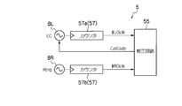
- FIG. 7 is a diagram illustrating an example of a calibration circuit that reduces variation in the oscillation frequency of the LC oscillator.
- the side channel attack detection apparatus according to the embodiment of the present invention has a mechanism for reducing variations in the PVT (process, voltage, temperature) of the oscillation frequency of the LC oscillator in order to improve the detection accuracy of the detection means.
- a ring oscillator is mounted locally, and the LC oscillation frequency is adaptively calibrated according to PVT variation.
- a ring oscillator 8R is provided in a sensor core circuit formed on the integrated circuit chip.
- the calibration circuit 55 is formed in the control circuit 5 (control unit) or the like.
- An LC oscillator 8L and a ring oscillator 8R are connected to the calibration circuit 55 via counters 57a (57) and 57b (57), respectively.
- the counter 57a (57) measures the oscillation frequency of the LC oscillator 8L and outputs a signal LOclk (#LOclk) to the calibration circuit 55.
- the counter 57b (57) measures the oscillation frequency of the ring oscillator 8R and outputs a digital signal ROclk (#ROclk) to the calibration circuit 55.
- FIG. 8 is a diagram illustrating an example of each characteristic of the oscillation frequency of each oscillator. Specifically, FIG. 8A shows the case of a ring oscillator, and FIG. 8B shows the case of an LC oscillator.
- FIG. 9 is a diagram for explaining an example of the calibration operation. 8A, 8B, and 9, the horizontal axis represents the supply voltage V DD [V], and the vertical axis represents the shift ratio [%] of the oscillation frequency.
- the left side of each of FF, TT, and SS shows NMOS characteristics
- the right side shows PMOS characteristics.
- FIG. 10 is a diagram illustrating an example of a conversion table (lookup table: LUT).
- the horizontal axis represents the frequency for calibration
- the vertical axis represents the capacitance value.
- the LC oscillator used for the sensor as the detection means does not use a varactor diode type capacitor having a positive temperature coefficient, but a small MOS capacitor for calibration (also has a positive temperature coefficient, but the temperature coefficient is Only smaller than the diode).
- the PVT variation in the oscillation frequency of the LC oscillator has a characteristic inversely proportional to g m of the transistor of the CMOS inverter, and has a monotonous inverse characteristic with respect to the frequency of the ring oscillator (see FIGS. 8 and 9). Although not shown in the graphs of FIGS. 8 and 9, the same applies to the SF / FS corner.
- counters 57a (57) and 57b (57) for counting the oscillation frequency of the LC oscillator 8L and the ring oscillator 8R and a small-sized LUT can be used.
- Digital calibration of the oscillation frequency can be performed in one step.
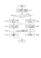
- FIG. 11 is a flowchart illustrating an example of the calibration operation of the oscillation frequency of the LC oscillation circuit using the calibration circuit. Next, an example of a method for calibrating the oscillation frequency of the LC oscillator will be described with reference to FIG. 4, FIG. 7 to FIG.
- step ST11 the control circuit 5 including the calibration circuit 55 activates the ring oscillator 8R, the LC oscillator 8L, and the counters 57a and 57b.
- the counter 57a measures the oscillation frequency of the LC oscillator 8L
- the counter 57b measures the oscillation frequency of the ring oscillator 8R.
- the counter 57a counts the number of clocks of the LC oscillator 8L
- the counter 57b counts the number of clocks of the ring oscillator 8R.
- the calibration circuit 55 reads the count value of the other counter when either one of the counters 57a and 57b reaches the full count (set value), and increases or decreases the calibration value accordingly.
- the calibration circuit 55 refers to an LUT (FIG. 10) stored in advance in a storage circuit or the like, converts the obtained calibration value into a capacitance value ( ⁇ C) of the LC oscillator 8L, and oscillates the LC oscillator 8L. Calibrate the frequency.
- step ST12 the calibration circuit 55 determines whether one of the measurement values counted by the counters 57a and 57b has reached a full count (set value), and the counter 57b (for the ring oscillator) is checked. If the count value (#ROclk) reaches the full count, the process proceeds to step ST13. If the count value (#LOclk) of the counter 57a (for the LC oscillator 8L) reaches the full count, the process proceeds to step ST23.
- step ST13 the calibration circuit 55 reads the count value (#LOclk) from the counter 57a (for the LC oscillator). This count value corresponds to the difference between the oscillation frequency of the ring oscillator and the oscillation frequency of the LO oscillator.
- step ST14 based on the count value (#LOclk) by the counter 57a (for the LC oscillator), a process of decreasing the calibration value is performed so that the oscillation frequency of the LC oscillator becomes the set value.
- step ST15 the calibration circuit 55 refers to the LUT (see FIG. 10), converts the calibration value (corresponding to ⁇ f) to the capacitance value ⁇ C of the LC oscillator, and proceeds to the process of step ST16.
- the calibration circuit 55 calibrates the oscillation frequency by reducing the capacitance of the LC oscillator 8L based on the capacitance value ⁇ C. Specifically, the calibration circuit 55 outputs the signal CalCode to the LC oscillator 8L, and turns on or off the transistors T21 to T2a and T2b to T2n shown in FIG. 4B according to the signal CalCode.
- the oscillation frequency of the LC oscillator 8L is calibrated by adjusting the capacitance values of the MOS capacitors by T11 to T1a and T1b to T1n.
- step ST23 when the count value (#LOclk) of the counter 57a (for the LC oscillator 8L) reaches a full count (step ST12), the calibration circuit 55 obtains the count value (#ROclk) by the counter 57b (for the ring oscillator). Read. This count value corresponds to the difference between the oscillation frequency of the ring oscillator and the oscillation frequency of the LO oscillator.
- step ST24 based on the count value (#ROclk) by the counter 57b (for the ring oscillator), the calibration value is increased so that the oscillation frequency of the LO oscillator becomes the set value, and the process proceeds to step ST15. .
- step ST15 the calibration circuit 55 refers to the LUT (see FIG. 10), converts the calibration value (corresponding to ⁇ f) to the capacitance value ⁇ C of the LC oscillator, and proceeds to the process of step ST26.
- step ST26 the calibration circuit 55 calibrates the oscillation frequency by increasing the capacitance of the LC oscillator 8L based on the capacitance value ⁇ C.
- the calibration circuit 55 uses the frequency difference between the LC oscillation circuit and the ring oscillation circuit, so that no other frequency reference is required. That is, the calibration process by the calibration circuit 55 is resistant to an attack in which an externally input clock source including the system clock is arbitrarily changed by an attacker. Further, in the above-described calibration method of the oscillation frequency of the LC oscillator using the calibration circuit 55, the capacitance is adjusted according to the LUT (conversion table) set in advance in the design stage, and only the PVT variation component of the oscillation frequency of the LC oscillator is obtained. The correction is performed, and the change in the oscillation frequency due to the change in the inductance accompanying the approach of the probe remains as it is after the calibration. Therefore, even if the probe is approached before the power is turned on, it is possible to detect attacks correctly based on the difference between the oscillation frequency in the specification (determined at the design stage) and the observed oscillation frequency after power-on / calibration. It is.
- the voltage characteristics of the ring oscillator and the voltage characteristics of the LC oscillator are opposite characteristics, and as shown in FIG. 9, a constant value passing through the intersection is obtained.
- Perform the above calibration That is, calibration is performed so as to reduce the voltage dependency of the oscillation frequency of the LC oscillator.
- the oscillation frequency of the ring oscillator is higher than the oscillation frequency of the LC oscillator, and the oscillation frequency of the LC oscillator is calibrated based on the frequency difference.
- the oscillation frequency of the ring oscillator is lower than the oscillation frequency of the LC oscillator, and the oscillation frequency of the LC oscillator is calibrated based on the frequency difference.
- the difference between the oscillation frequency of the ring oscillator and the oscillation frequency of the LC oscillator can determine whether the supply voltage is lower or higher than the reference voltage. Even in such a case, the oscillation frequency of the LC oscillator can be determined. Can be reliably calibrated.
- the temperature characteristics of the ring oscillator and the temperature characteristics of the LC oscillator are opposite characteristics, and as shown in FIG. Perform the above calibration.
- the oscillation frequency of the ring oscillator decreases as the temperature increases, and the oscillation frequency of the LC oscillator increases as the temperature increases.
- the calibration curve having a substantially constant value passing through the intersection is only slightly high. For this reason, even if the temperature changes, the calibration error can be made very small. That is, since the temperature dependence of the ring oscillation circuit and the LC oscillation circuit is opposite, drift due to temperature fluctuation can be reduced when correcting the voltage dependence.
- the process variation characteristics of the ring oscillator and the LC oscillator are reversed, and similarly, even if there is a process variation, the calibration error can be made very small. Can do.
- the inventor of the present application forms a coil L1 and a coil L2 on an integrated circuit chip having an encryption processing circuit 3a as the information processing apparatus 3 as shown in FIG.
- the sensor core circuit 50 that is, the LC oscillator having the coil L1, the LC oscillator having the coil L2, the control circuit 5, and the like were fabricated as an LSI of 0.18 ⁇ m CMOS technology.
- the coil L1 has 4 turns and the coil L2 has 3 turns.
- the coil L1 has a rectangular shape of 285 ⁇ m ⁇ 400 ⁇ m in length, and the coil L2 has a rectangular shape of 285 ⁇ m x width of 480 ⁇ m.
- An evaluation board equipped with an LSI having a detection device according to the present invention is mounted on a side channel attack standard evaluation board (SASEBO R-II), and a minimal electromagnetic probe fixed by a micromanipulator is brought close to the LSI having the detection device. It was.
- SASEBO R-II side channel attack standard evaluation board
- the EM signal from the probe was amplified with a 100 W power amplifier, the waveform was taken into a computer (PC) via an oscilloscope, and correlation calculation was performed with the computer to perform a local EM analysis attack.
- PC computer
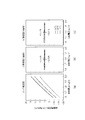
- FIG. 12 is a diagram showing an example of the measured power supply voltage and temperature dependence of the oscillation frequency of each oscillator. Specifically, FIG. 12A shows a case of a ring oscillator, FIG. 12B shows a case of an LC oscillator (3 windings), and FIG. 12C shows a case of an LC oscillator (4 windings). .
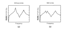
- FIG. 13 is a diagram illustrating an example of a frequency spectrum. Specifically, FIG. 13A shows the case of the three-turn coil L2 (no probe approach), FIG. 13B shows the case of the four-turn coil L1 (no probe approach), and FIG. 13C shows the three-turn coil L2. FIG. 13D shows the case of the 4-turn coil L1 (probe approaching L1).
- FIG. 14 is a diagram for explaining an example of an operation based on detection of a side channel attack.
- FIGS. 14A and 14B are diagrams showing an example of an electromagnetic wave waveform and an example of a correlation coefficient when there is no operation switching by attack detection
- FIGS. (D) is a figure which respectively shows an example of the electromagnetic wave waveform in the case of operation
- the control circuit can prevent the leakage of key information by causing the cryptographic processing circuit to perform an operation for performing leakage prevention processing such as stop or execution of a dummy operation after the side channel attack detection device detects the attack. This could also be confirmed by actual measurement. Specifically, as shown in FIG. 14, the detection of the correct key based on the correlation coefficient could be prevented.
- Table 1 shows the function of the side-channel attack detection apparatus according to the present invention and the area, power, and performance overhead when mounted on the cryptographic processing circuit (AES cryptographic circuit based on a 1 round / 1 clock loop architecture).
- the side channel attack detection device (the countermeasure circuit) according to the present invention has a 2.4% area, 1% power, and a small overhead of performance, and a local electromagnetic wave analysis that is difficult to prevent by conventional countermeasures. Can withstand attacks.
- the side channel attack detection device can be combined with preceding side channel attack countermeasures such as hiding and masking, and realizes a cryptographic processing circuit with more robust security by complementary combination. it can.
- the side channel attack detection device employs an LC oscillator including a coil (inductor) as detection means, and a probe composed of a conductor or the like.
- the control circuit as the determination means determines the approach of the probe or the opening of the LSI package due to the side channel attack based on the change in the oscillation frequency in accordance with the change in ().
- the detection device is based on a change in capacitance (mutual capacitance) due to the approach of the probe, etc.
- a determination unit such as a control circuit for determining approach of the probe due to an attack or opening of the LSI package may be included.
- FIG. 15 is a conceptual diagram for explaining an example of a side channel attack detection apparatus according to another embodiment of the present invention.
- FIG. 16 is a diagram illustrating an example of a transfer function. Specifically, FIG. 16A is a diagram illustrating an example of a transfer function when the probe is not approaching the detection unit, and FIG. 16B is an example of a transfer function when the probe is approaching the detection unit.
- FIG. FIG. 17 is a diagram illustrating an example of the frequency characteristic of the voltage of the input signal.
- the detection device according to the present invention shown in FIG. 15 forms a capacitor by providing a narrow transmission path 201 with a conductor as a detection means in the vicinity of the information processing device 3 formed on the integrated circuit chip 10. Then, a predetermined signal (see FIG.
- the control circuit 5 as a determination unit is based on the signal.
- the approach of the probe 7 may be determined by a change in the transfer function. That is, in the example shown in FIG. 16, the control circuit 5 as the determination unit approaches the probe due to the side channel attack based on the output indicating the capacitive coupling change (capacitance change) due to the approach of the probe 7 by the detection unit. Determine.
- an LSI integrated circuit chip 10
- the detection device has a capacity by opening the package.
- a capacitor is formed by providing a transmission path 201 with a conductor or the like as a detection means in the vicinity of the information processing device 3 formed on the integrated circuit chip 10.
- a predetermined signal (see FIG. 17) is input from one end, the signal is received at the other end of the transmission path 201, and the control circuit 5 serving as a determination unit based on the change of the transfer function is included in the LSI package. Opening may be determined.
- the control circuit 5 as the determination unit determines whether the LSI package is opened based on the change in capacitance coupling (capacitance change) due to the capacitive coupling when the package is opened.
- the side channel attack detection device 1 includes a coil (inductor) or a capacitor disposed in the vicinity of the information processing device that is the target of the side channel attack, It has a detecting means for detecting a change in the inductance of the coil (inductor) or the capacitance of the capacitor, and a control circuit 5 as a determining means for judging the approach of the probe or the opening of the LSI package due to the side channel attack by the detecting means. For this reason, it is possible to provide a detection device capable of detecting a side channel attack with a simple configuration. Further, when the approach of the probe due to the side channel attack or the opening of the LSI package is detected, the control circuit may perform a process of switching to the operation mode for protecting the secret information of the cryptographic processing circuit as described above.
- the detection apparatus according to the present invention has the above-described detection means, it is possible to prevent all side channel attacks using electrical information by probing, including local electromagnetic wave analysis attacks that are difficult to prevent with conventional countermeasures.
- the detection apparatus changes the inductance of the coil, more specifically, for example, when the probe is brought close to measure the electromagnetic field radiated from the wiring pattern on the integrated circuit or on the printed circuit board.
- Side channel attacks can be detected based on the physical law that the degree of electromagnetic field coupling between the circuit and wiring on the printed circuit board and the surroundings (including the probe) changes, and the electromagnetic field distribution inevitably changes. It is difficult for an attacker to attack without being detected in principle.
- the overhead such as the execution speed, power consumption, and mounting area of the cryptographic LSI is greatly reduced as compared with the conventional countermeasures.
- Conventional measures increase the circuit scale at least several times.
- the detection means is constituted by an LC oscillator, it can be realized with a slight area overhead of 2.4% with respect to the encryption processing circuit to be countermeasured.
- the area can be reduced in the same manner as the cryptographic core according to the miniaturization of the integrated circuit manufacturing process.
- the coil can be reduced by improving the transistor performance by miniaturizing the integrated circuit manufacturing process, and the area overhead of the entire sensor with respect to the cryptographic core can be kept constant.
- the detection means when the detection means is constituted by an LC oscillator, circuits other than the coil can be constituted by a completely digital circuit (logic circuit), so that the design is easy and the integrated circuit manufacturing process is miniaturized. Accordingly, the area can be reduced in the same manner as the cryptographic core.
- the detection device can detect various probing methods and eliminate the need for a high-accuracy frequency reference by using an attack detection method using two or more coils having different shapes and winding numbers. This makes it impossible to attack the frequency reference.
- the attack detection method using two or more coils eliminates the need for a high-accuracy frequency reference and makes it impossible to attack the frequency reference, and greatly increases the circuit area and power consumption according to the present invention. Contributes to reduction. Furthermore, it is possible to cope with variations in PVT by one-step digital calibration of a sensor using a ring oscillator.
- the present invention can be realized with a small area overhead of, for example, about 2.4% with respect to a cryptographic processing circuit (information processing apparatus) as a countermeasure target.
- a semiconductor device having the side channel attack detection device can be provided. Further, according to the present invention, a side channel attack detection method by the side channel attack detection device can be provided.
Landscapes
- Engineering & Computer Science (AREA)
- Computer Security & Cryptography (AREA)
- Computer Networks & Wireless Communication (AREA)
- Signal Processing (AREA)
- Semiconductor Integrated Circuits (AREA)
- Electronic Switches (AREA)
Abstract
簡単な構造で、サイドチャネル攻撃を検知することができる検知装置を提供すること。 サイドチャネル攻撃の検知装置1は、サイドチャネル攻撃の対象となる暗号処理回路3aなどの情報処理装置3に近接して配置されたインダクタとしてのコイルLまたはキャパシタを有し、コイルL(インダクタ)のインダクタンスまたはキャパシタのキャパシタンスの変化を検知する検知手段2と、検知手段2の出力に基づいてサイドチャネル攻撃によるプローブ7の接近またはLSIパッケージの開封を判定する判定手段(制御回路5)と、を有する。
Description
本発明は、サイドチャネル攻撃の検知装置、サイドチャネル攻撃の検知装置によるサイドチャネル攻撃の検知方法に関し、特に、暗号工学分野のうち、暗号LSIなどの情報処理装置に対するサイドチャネル攻撃の対策技術に関する。
情報通信機器の携帯が一般的となり、ネットワーク上でのプライバシ保護や高信頼な電子商取引の重要性がますます高まっている。暗号はそのような社会システムを構築する上で欠かすことのできない基盤技術であり、暗号アルゴリズムを実現したソフトウェアやハードウェアが動作する大規模集積回路(以下、暗号LSIと呼ぶ)は多くの民生品に搭載されている。暗号LSIには、通常、専門家により十分に安全性評価を行った暗号アルゴリズムが利用される。そのため、アルゴリズムの欠陥から暗号化前のデータ(平文)や秘密鍵などの漏洩の心配は(現在の計算機能力や知られている解読法の観点から)ほとんどない。
一方、暗号LSIの実装上の脆弱性から現実的な時間で秘密情報を奪う実装攻撃の脅威が指摘されている。特に注目を集めているのが、暗号LSIの演算中の消費電力や放射電磁波、実行時間等といった本来の入出力以外の情報(サイドチャネル情報)を観察することで秘密情報を奪うサイドチャネル攻撃である。
サイドチャネル攻撃の中でも最もよく知られる攻撃が電力・電磁波解析攻撃である。1990年代後半にKocherらによって単純電力解析と差分電力解析が発表されたのを機に、その拡張が盛んに研究され始めた。その後、電力の代わりに漏洩電磁波の波形を用いた電磁波解析攻撃が可能であることが示された。
電力解析攻撃や電磁波解析攻撃では、測定用プローブとデジタルオシロスコープを用いて暗号LSIから漏洩する電流・電圧の時間変化を計測する。計測した波形を計算機で加工・処理して暗号処理の内容や秘密鍵の値を推定する。
電力解析攻撃や電磁波解析攻撃では、測定用プローブとデジタルオシロスコープを用いて暗号LSIから漏洩する電流・電圧の時間変化を計測する。計測した波形を計算機で加工・処理して暗号処理の内容や秘密鍵の値を推定する。
特に、電磁波解析攻撃は、機器に直接プロービングしてLSI全体の過渡的な電圧変化を測定する電力解析と比べ、非接触な攻撃が可能となる。また、暗号LSIの局所的な特性を取得できることが報告されており、これまで電力解析の適用は難しいとされてきた機器に対しても脅威となる可能性が指摘されている。とりわけ、近年、一般的な暗号LSIの最小構成素子(ANDやXOR等の基本ゲート)の非対称性により、秘密情報を処理する部分の局所的な電磁波放射から原理的に秘密情報を取得できることが報告されている(例えば、非特許文献1参照)。
従来のサイドチャネル攻撃への対策は、秘密情報と相関のある中間値をサイドチャネル情報として漏洩させないことを目的とし、主に乱数によって中間値を遮蔽するマスキングもしくは中間値を隠ぺいするハイディングという概念で実現されてきた。これまでアルゴリズムレベルやロジックレベル(デジタル回路レベル)で数多くのサイドチャネル攻撃への対策が提案されている(例えば、非特許文献2参照)。
T. Sugawara, et al., "On Measurable Side-Channel Leaks Inside ASIC Design Primitives," Proc. CHES, pp.159-178, Aug. 2013.
K. Tiri and et al., "Prototype IC with WDDL and differential routing - DPA resistance assessment," CHES 2005, Lecture Notes in Computer Science, vol. 3659, pp. 354-365, May 2005.
S. Mangard, E. Oswald, and T. Popp, "Power Analysis Attacks - Revealing the Secrets of Smart Cards," Springer, 2007.
しかしながら、上述した従来のアルゴリズムレベルやロジックレベル(デジタル回路レベル)でのサイドチャネル攻撃への対策では、ANDやXOR演算中の情報は漏洩しないことを前提としているため、その前提を覆す非特許文献1に記載されている攻撃に対しては原理的に対処できない。その前提を実現するためには基本演算素子の設計まで考慮したトランジスタレベルの対策が必要となるが、仮にそうした対策が実現できても、それは従来よりも設計難易度・コストを大幅に高める上に、暗号LSIの実行速度や消費電力、実装面積などを大きく増加させてしまう。
例えば、ロジックレベルのハイディング対策として知られるWDDL(Wave Dynamic Differential Logic)(非特許文献2参照)では、非特許文献1に記載されている攻撃に対処できない。さらに,同対策は少なくとも回路規模を数倍程度増加させることが知られている。
アナログ回路レベルの対策として、暗号LSIの消費電力を内部動作状態に関わらず均一化する電源電流イコライザ(例えば、非特許文献3参照)も提案されており、それらは比較的低オーバーヘッド(回路規模2倍程度の増加)で実現でき、電力解析攻撃には有効であるが、やはり非特許文献1に記載されているサイドチャネル攻撃には対処できない。
本発明は、このような問題に対処することを課題の一例とするものである。すなわち、簡単な構成で、サイドチャネル攻撃を検知可能な検知装置を提供すること、サイドチャネル攻撃の検知方法を提供すること、などを目的とする。
このような目的を達成するために、本発明によるサイドチャネル攻撃の検知装置は、サイドチャネル攻撃の対象となる情報処理装置に近接して配置されたインダクタを有し、前記インダクタのインダクタンスの変化を検知する検知手段と、前記検知手段の出力に基づいて前記サイドチャネル攻撃によるプローブの接近またはLSIパッケージの開封を判定する判定手段と、を有することを特徴とする。
また、本発明に係るサイドチャネル攻撃の検知装置は、サイドチャネル攻撃の対象となる情報処理装置に近接して配置されたキャパシタを有し、前記キャパシタのキャパシタンスの変化を検知する検知手段と、前記検知手段の出力に基づいて前記サイドチャネル攻撃によるプローブの接近またはLSIパッケージの開封を判定する判定手段と、を有することを特徴とする。
また、本発明のサイドチャネル攻撃の検知方法は、上記本発明に係るサイドチャネル攻撃の検知装置を用いて行われる。
本発明によれば、簡単な構造で、サイドチャネル攻撃を検知可能な検知装置を提供することができる。また、本発明によれば、検知装置を用いることで簡単にサイドチャネル攻撃を検知することが可能なサイドチャネル攻撃の検知方法を提供することができる。
本発明に係る検知装置は、サイドチャネル攻撃そのものを検知する。詳細には、本発明に係るサイドチャネル攻撃の検知装置は、サイドチャネル攻撃の対象となる情報処理装置に近接して配置されたインダクタまたはキャパシタを有し、インダクタ(コイル)のインダクタンスまたはキャパシタのキャパシタンスの変化を検知する検知手段を備え、その検知手段の出力に基づいてサイドチャネル攻撃によるプローブ(導電体などにより構成される)の接近またはLSIパッケージの開封などを判定する判定手段と、を有する。本発明に係る検知装置は、プローブの接近やLSIパッケージの開封時など、インダクタンスやキャパシタンスの変化を検知手段で検知し、判定手段にてサイドチャネル攻撃を容易に判定することができる。
従来のサイドチャネル攻撃への対策は、攻撃されていることを検知できないことが前提となっており、有意なサイドチャネル情報を漏洩させないことが目的となっていた。本発明に係る検知装置は、電磁気の物理法則に基づいてサイドチャネル攻撃を検知することができ、その攻撃を検知した場合、以降の暗号処理を停止・変更するなどの処理を行うことで、秘密情報の漏洩を防ぐ。
また、検知装置は、例えば、情報処理装置としての暗号LSI(暗号アルゴリズムを実現したソフトウェアやハードウェアが動作する大規模集積回路)に対するサイドチャネル攻撃(暗号LSIの動作中に生じる副次的な情報(サイドチャネル情報)を観察することで秘密情報を奪う攻撃)を検知する。本発明に係る検知装置などの技術の実現にあたっては、集積回路工学と環境電磁工学の理論と技術などを応用している。
また、サイドチャネル攻撃の手段としてのプローブが情報処理装置としての暗号LSI(暗号処理回路)などに接近している場合、本発明の実施形態に係る検知装置は、それをプローブによって生じるインダクタンスの変化として、電磁界の乱れ(それに伴う情報処理装置の近傍電磁界や回路内部の特性インピーダンスの変化、回路内部を流れる信号損失の発生などの電気的パラメータの変化)から検知可能であり、局所電磁波解析攻撃を含むプロービングによる電気的情報を用いるサイドチャネル攻撃全般を防ぐ。上記電気的パラメータの変化は、プローブと暗号LSIとの電界結合、磁界結合、もしくはその両方により生ずるため、これらを避けてプロービングを伴う攻撃を実行することは原理的に困難である。
本発明の実施形態に係る検知装置の攻撃検知センサ部分(検知手段)は、後述するように、インダクタ(コイル)を含むLC発振器などの簡便な回路で実現可能であり、センシング後段の処理回路を含めても対策対象となる暗号LSI(情報処理装置)対して僅か数パーセントという面積オーバーヘッドで実現できる。
環境電磁工学の分野では、集積回路内部やプリント基板上の配線パターン近傍から放射される電磁界に測定用プローブを接近配置すると、電磁界分布に変化が生じる物理現象がよく知られている。検知装置は、この物理現象を応用して、攻撃時にプローブが暗号LSIに接近する際に生じる電磁界の乱れをサイドチャネル攻撃の検知に用いる。攻撃検知後に秘密情報を保護する処理(例えば暗号処理の停止やダミー演算の挿入など動作モードを切り替える処理)で秘密情報の漏洩を防ぐことができる。
図1は本発明の実施形態に係るサイドチャネル攻撃の検知装置を用いたサイドチャネル攻撃の検知方法の一例を示すフローチャートである。図2は本発明の実施形態に係るサイドチャネル攻撃の検知装置1の一例を示す図である。
図2に示した例では、集積回路チップ10に、サイドチャネル攻撃の対象であり、防御対象の情報処理装置3である暗号処理回路3aや防御対象としての秘密鍵を記憶する記憶回路3bなどが形成されている。
検知装置1は、サイドチャネル攻撃を検知する検知手段2を有する。検知手段2としては、例えば、コイルL(インダクタ)を含むLC発振器などを採用することができ、集積回路チップ10などに形成されている。つまり、情報処理装置3と検知手段2は、同一の集積回路チップ10に設けられている。本実施形態では、LC発振器のコイルL(インダクタ)は、情報処理装置3と一体もしくは情報処理装置3の近傍に配置されている。図2に示した例では、防御対象の情報処理装置3である暗号処理回路3aの周囲を囲むように、検知手段2であるLC発振器のコイルLが形成されている。
検知装置1は、サイドチャネル攻撃を検知する検知手段2を有する。検知手段2としては、例えば、コイルL(インダクタ)を含むLC発振器などを採用することができ、集積回路チップ10などに形成されている。つまり、情報処理装置3と検知手段2は、同一の集積回路チップ10に設けられている。本実施形態では、LC発振器のコイルL(インダクタ)は、情報処理装置3と一体もしくは情報処理装置3の近傍に配置されている。図2に示した例では、防御対象の情報処理装置3である暗号処理回路3aの周囲を囲むように、検知手段2であるLC発振器のコイルLが形成されている。
また、検知装置1は、検知手段2の出力に基づいて、サイドチャネル攻撃によるプローブの接近やLSIパッケージの開封を判定する判定手段としての制御回路5などを有し、制御回路5は、サイドチャネル攻撃を検知した場合に情報漏洩を防止する所定の処理などを行う。この判定手段としての制御回路5は、集積回路チップ10に形成されている。尚、制御回路5は、別の集積回路チップに形成されていてもよい。
図3は、検知手段としてのLC発振器の発振周波数のシフトからサイドチャネル攻撃を検知する一例を示す図である。詳細には、図3は検知手段としてのLC発振器の周波数スペクトラムの一例を示し、横軸に発振周波数を示し、縦軸に各周波数成分の大きさを示す。
電磁プローブ(プローブ)の接近により、コイルLの等価インダクタンスが変化する。このインダクタンスの変化に伴うLC発振器の発振周波数foscのシフトに基づいて、サイドチャネル攻撃を検知する。
詳細には、プローブ7が情報処理装置3の近傍に配置された検知手段2に接近していない場合(P1)、検知手段2としてのLC発振器の発振周波数foscは近似的に数式(1)に示すようになり、プローブ7が検知手段2に接近した場合(P2)、LC発振器の発振周波数foscはプローブ7とコイルLとの間の相互インダクタンスMにより、近似的に数式(2)に示すようになる。プローブ7の接近により相互インダクタンスMが大きくなり、発振周波数foscが大きくなる。つまり、検知手段2により取得されたLC発振器の発振周波数foscが大きくシフトするなどし、予め規定された閾値を超えたか否かに基づいて、制御回路5がプローブ7の接近を検知することが可能である。プローブ7の接近を検知した場合、制御回路5は暗号処理回路の動作モードを、例えば、暗号化停止処理やダミー鍵を用いた処理などに切り替えることで、秘密情報などの漏洩を回避する。
詳細には、プローブ7が情報処理装置3の近傍に配置された検知手段2に接近していない場合(P1)、検知手段2としてのLC発振器の発振周波数foscは近似的に数式(1)に示すようになり、プローブ7が検知手段2に接近した場合(P2)、LC発振器の発振周波数foscはプローブ7とコイルLとの間の相互インダクタンスMにより、近似的に数式(2)に示すようになる。プローブ7の接近により相互インダクタンスMが大きくなり、発振周波数foscが大きくなる。つまり、検知手段2により取得されたLC発振器の発振周波数foscが大きくシフトするなどし、予め規定された閾値を超えたか否かに基づいて、制御回路5がプローブ7の接近を検知することが可能である。プローブ7の接近を検知した場合、制御回路5は暗号処理回路の動作モードを、例えば、暗号化停止処理やダミー鍵を用いた処理などに切り替えることで、秘密情報などの漏洩を回避する。

次に、サイドチャネル攻撃の検知動作の一例について説明する。
ステップST1において、攻撃検知センサであるコイルLを含むLC発振器などの検知手段2を起動する。ここで、起動する検知手段2は、防御対象となる暗号処理回路3aなどと一体もしくはその近傍に設置され、任意の方向から暗号処理回路3aなどに接近するもしくはあらかじめ接近しているプローブ7によって生じるコイルL(インダクタ)のインダクタンスの変化、詳細には、電磁界の乱れ(それに伴う近傍電磁界や回路内部の特性インピーダンスの変化、回路内部を流れる信号損失の発生など)を観測可能とする。例えば、情報処理装置3として暗号処理回路3aなどを採用した場合、検知手段2としてのセンサは当該回路の内部に実装されるように構成してもよい。
ステップST1において、攻撃検知センサであるコイルLを含むLC発振器などの検知手段2を起動する。ここで、起動する検知手段2は、防御対象となる暗号処理回路3aなどと一体もしくはその近傍に設置され、任意の方向から暗号処理回路3aなどに接近するもしくはあらかじめ接近しているプローブ7によって生じるコイルL(インダクタ)のインダクタンスの変化、詳細には、電磁界の乱れ(それに伴う近傍電磁界や回路内部の特性インピーダンスの変化、回路内部を流れる信号損失の発生など)を観測可能とする。例えば、情報処理装置3として暗号処理回路3aなどを採用した場合、検知手段2としてのセンサは当該回路の内部に実装されるように構成してもよい。
ステップST2において、検知手段2としてのセンサを用いて、コイルL(インダクタ)のインダクタンスの変化、詳細には、電磁界の乱れなど、センサと周囲との電磁界結合度の変化(もしくはそれに伴う物理量)を取得する。例えば、検知手段2を、コイルL(インダクタ)を含むLC発振器で実現した場合、センサと周囲との電磁界結合度の変化はLC発振器の発振周波数の変化として得られる。つまり、検知手段2は、コイルL(インダクタ)のインダクタンスの変化を、LC発振器の発振周波数の変化により検知している。さらに、センサを複数の形状・巻き数の異なるコイルにより構成すれば、電磁界結合度の変化は各コイルの発振周波数の相対的な変化として得られる。このとき、絶対的な周波数基準が不要となり、相対的に大きな基準周波数発生回路を省略できるだけでなく、周波数基準を悪用する攻撃の危険性を排除できる。
ステップST3において、検知手段2により、プローブの接近やパッケージの開封によるコイルのインダクタンスの変化を検知したか否かを、詳細には、電磁界の乱れなど、電磁界結合度の変化を観測したか否かを判定手段としての制御回路5(制御部)などが判定する。詳細には、制御回路5は、例えば、検知手段2をコイルLを含むLC発振器(コイル)で実現した場合、コイルLの発振周波数の変化、つまりコイルLのインダクタンスの変化により判定する。これが変化している場合にはステップST4の処理に進み、変化していない場合にはステップST5の処理に進む。
ステップST4において、検知手段2により上記変化が観測された場合、制御回路5は攻撃検知信号を出力する。ここでは、制御回路5が暗号処理回路3aなどに攻撃検知信号を出力した場合、暗号処理回路3aは秘密情報を保護する動作モード(停止やダミー演算の実行、ハイディング処理、マスキング処理)などに切り替える処理を行う。
尚、制御回路5は、秘密情報を保護する動作モードに切り替える処理として、少なくとも、偽の鍵を用いた暗号処理、鍵の変更処理、暗号処理に関わる情報(例えば、少なくとも、鍵、データ、回路情報のいずれかを含む)を消去する処理、検知したことを外部に通知する処理、のいずれかを行ってもよい。
尚、制御回路5は、秘密情報を保護する動作モードに切り替える処理として、少なくとも、偽の鍵を用いた暗号処理、鍵の変更処理、暗号処理に関わる情報(例えば、少なくとも、鍵、データ、回路情報のいずれかを含む)を消去する処理、検知したことを外部に通知する処理、のいずれかを行ってもよい。
ステップST5において、検知手段2としてのセンサにより上記変化が観測されなかった場合、防御対象となる暗号処理回路などの暗号化処理が終了するまでステップST2,ST3の処理を適宜繰り返す。
図1に示した処理の頻度は防御する対象に応じて変更する。例えば、単純解析の対象となる公開鍵暗号処理の場合、各鍵ビットの演算が行われる間隔で処理(ステップST2,ST3)を繰り返す。差分解析の対象となる共通鍵暗号処理の場合、暗号処理の直前に一度だけ処理(ステップST2,ST3)を行う。
<複数のLC発振器を攻撃検知センサとして用いた検知装置>
図4は本発明の実施形態に係る検知装置1の一例を示す図である。詳細には、図4(a)は複数のLC発振器を有する検知装置1の概念図、図4(b)は図4(a)に示した検知装置1の一具体例を示す回路図である。検知手段2は、複数のLC発振器(発振回路)を備えていてもよい。以下、検知手段2として2つのLC発振器を備えた検知装置1を説明する。
図4は本発明の実施形態に係る検知装置1の一例を示す図である。詳細には、図4(a)は複数のLC発振器を有する検知装置1の概念図、図4(b)は図4(a)に示した検知装置1の一具体例を示す回路図である。検知手段2は、複数のLC発振器(発振回路)を備えていてもよい。以下、検知手段2として2つのLC発振器を備えた検知装置1を説明する。
詳細には、検知装置1は、情報処理装置3としての暗号処理回路3a上またはその近傍に配置されたコイルL1,コイルL2を有する。また、検知装置1は、コイルL1,L2をそれぞれ備えた発振器51(LC発振器を含む),発振器52(LC発振器を含む)、およびセンサコア回路50を有する。例えば、暗号処理回路3aの秘密情報処理部3c,3dなどの秘密情報を処理する機能ブロック(S-BOXやレジスタ等)は、それぞれコイルL1,L2の直下に配置し、それ以外の鍵情報を含まない機能ブロック(I/Oインタフェース等)をコイルL1,L2間に配置する。
センサコア回路50は、例えば、制御回路5(制御部)と、コイルL1用の発振器51(発振回路)、コイルL2用の発振器52(発振回路)を有する。各発振器51,52のコイルL1,L2は上述したように、秘密情報処理部3c,3dの近傍に配置されている。詳細には、検知手段は、少なくともコイルL1(センサコイル)、コイルL2(センサコイル)などのコイルを有する。本実施形態では、検知手段は、コイルL1,L2などのコイル、センサコア回路50(制御回路5(制御部)、発振器51,52などの発振器、較正回路、リング発振器等)、などを有する。
コイルL1,L2は、例えば、直交する辺を異なる配線層でレイアウトすることで、各コイル下に配置される暗号処理回路3aのデジタル信号配線を妨害しないように構成されている(例えば、非特許文献参照:M. Saito, et al., “An Extended XY Coil for Noise Reduction in Inductive-coupling Link,” A-SSCC Dig. Tech. Papers, pp.305-308, Nov. 2009.)。
コイルL1,L2に必要なリソースは、数10トラック程度の配線リソースのみである。
検知手段2としての2つのコイルL1,L2は、巻き数や直径等の形状が同じであってもよいし、異なるものを用いてもよい。
本実施形態では、検知手段2としての2つのコイルL1,L2は、巻き数や直径等の形状の異なるものを用いる。例えば、サイドチャネル攻撃時にプローブを用いて秘密情報を取得するためには、2つのコイルL1,L2のいずれか一方もしくは両方に接近させる必要がある。プローブが接近した場合、2つの発振器51,52(LC発振器)の発振周波数に差が生じる。ここで、2つのコイルL1,L2の巻き数・形状が異なるため、コイルL1,L2にまたがったプローブの接近(一般的な電磁波解析攻撃)や個々のコイルL1,L2に対して同一のプローブが同時に接近(複数のプローブによる電磁波解析攻撃)した場合であっても、各発振器51,52(LC発振器)の発振周波数に差が生じることに注意されたい。
検知手段2としての2つのコイルL1,L2は、巻き数や直径等の形状が同じであってもよいし、異なるものを用いてもよい。
本実施形態では、検知手段2としての2つのコイルL1,L2は、巻き数や直径等の形状の異なるものを用いる。例えば、サイドチャネル攻撃時にプローブを用いて秘密情報を取得するためには、2つのコイルL1,L2のいずれか一方もしくは両方に接近させる必要がある。プローブが接近した場合、2つの発振器51,52(LC発振器)の発振周波数に差が生じる。ここで、2つのコイルL1,L2の巻き数・形状が異なるため、コイルL1,L2にまたがったプローブの接近(一般的な電磁波解析攻撃)や個々のコイルL1,L2に対して同一のプローブが同時に接近(複数のプローブによる電磁波解析攻撃)した場合であっても、各発振器51,52(LC発振器)の発振周波数に差が生じることに注意されたい。
コイルL1,L2以外のセンサコア回路50は、完全デジタル回路で構成されている。LC発振器のコアは、電源スイッチ付きのCMOSインバータなどで構成されている。詳細には、発振器51(LC発振回路)は、コイルL1(インダクタ)を除きロジック回路で構成されている。
発振器51が形成された集積回路は、複数のトランジスタT1~T3,T11~T1a,T1b~T1n,T21~T2a,T2b~Tbn、インバータN1~N8,N11~N14、NANDゲートD1,D11などを有し、図4(b)に示したように各構成要素が接続されている。
本実施形態では、例えば、MOS型電界トランジスタのキャパシタとコイルL1を用いて発振器51(8L)を構成している。発振器51(LC発振器)の発振周波数は、予め規定された周波数となるように設定されており、各トランジスタT11~T1a,T1b~T1n,T21~T2a,T2b~Tbnの接続を切り替えることにより、発振周波数の微調整を行うことができるように構成されている。
発振器51が形成された集積回路は、複数のトランジスタT1~T3,T11~T1a,T1b~T1n,T21~T2a,T2b~Tbn、インバータN1~N8,N11~N14、NANDゲートD1,D11などを有し、図4(b)に示したように各構成要素が接続されている。
本実施形態では、例えば、MOS型電界トランジスタのキャパシタとコイルL1を用いて発振器51(8L)を構成している。発振器51(LC発振器)の発振周波数は、予め規定された周波数となるように設定されており、各トランジスタT11~T1a,T1b~T1n,T21~T2a,T2b~Tbnの接続を切り替えることにより、発振周波数の微調整を行うことができるように構成されている。
リング発振器8Rは、図4(b)に示したように、インバータN11~N14、NANDゲートD11により構成されている。このリング発振器8Rは、発振器51のLC発振器8Lの発振周波数を較正する際に用いられる。
発振器52(LC発振器を含む)は、上述した発振器51と略同様な構造であり、コイルL1をコイルL2と読み替えた構造であるので、説明を省略する。つまり、発振器52は、LC発振器、リング発振器などを有する。
図5は2つのLC発振器の周波数差によるサイドチャネル攻撃の検知の一例を説明する図である。詳細には、コイルL1を有するLC発振器の発振周波数と、コイルL2を有するLC発振器の発振周波数を図5に示す。図5において、横軸に検知手段(センサ)としてのコイルL1,L2とプローブとの距離を示し、縦軸に発振周波数を示す。
図5に示した例では、サイドチャネル攻撃によるプローブがコイルL1,L2から離れている場合、各LC発振器の発振周波数は、閾値fthより小さい同じ値を示すとする。尚、各LC発振器の発振周波数は異なる値を示していてもよい。
例えば、プローブがコイルL2に近づいた場合、コイルL1を有するLC発振器の発振周波数は僅かに上昇し、コイルL2を有するLC発振器の発振周波数は閾値fthより大きい値を示す。また、プローブがコイルL1に近づいた場合、コイルL1を有するLC発振器の発振周波数が閾値fthより大きい値を示すことになる。
上述したように、検知手段としてコイルL1,L2を用いた場合、コイルL1,L2の一方または両方に近づいたことを、各LC発振器の発振周波数に基づいて容易に検知することができる。
上述したように、検知手段としてコイルL1,L2を用いた場合、コイルL1,L2の一方または両方に近づいたことを、各LC発振器の発振周波数に基づいて容易に検知することができる。
尚、各発振器51,52(LC発振器)の発振周波数差は制御回路内のカウンタで計測される。本発明の実施形態に係る検知装置は、検知手段として発振器51,52(LC発振器)の発振周波数差を利用しており、クロックを周波数基準として使用しないため、システムクロックを含む外部入力のクロック源が攻撃者によって任意に変更される攻撃に対して耐性を有する。また、面積と電力の大きいオンチップの高精度な周波数基準発生回路(バンドギャップリファレンスなどのアナログ回路)も不要となる。物理サイズを考慮すると困難ではあるが、万が一、2つの電磁プローブで2つのコイルを同時に攻撃しても、コイル形状が異なるため、両コイルの周波数シフト量を長時間一定に保つのは極めて困難である(攻撃には数時間かかる)。
図6は検知装置と情報処理装置(暗号処理回路)の動作の一例を示すタイミングチャートである。詳細には、図6(a)は暗号処理回路の動作の一例を示す図、図6(b)はLC発振回路に関する信号LOenの一例を示す図、図6(c)はリング発振回路に関する信号ROenの一例を示す図である。
本実施形態に係る検知装置は、検知手段としてのLC発振回路を、図6に示すように、暗号処理の動作前後に間欠起動することで、プローブの接近をモニタする。動作間隔は守るべき暗号アルゴリズムに応じて適宜設定することができる。
図6に示した例では、トリガ信号LOenによってLC発振器は、起動時に即座にフルスイング(設定振幅)の安定発振を行うことができる。トリガ信号ROenによりリング発振器は所定の発振周波数で発振を行う。後述するように、本発明の実施形態に係る検知装置は、リング発振器による発振周波数とLC発振器による発振周波数に基づいて、LC発振器の周波数を較正する。
サイドチャネル攻撃の検知に必要な時間は、1μs以下であり、I/Oを含む暗号処理時間(~100μs)の1%以下の動作時間に抑えることができるため、消費電力のオーバーヘッドを著しく低減できる。
LC発振器は、暗号処理動作の停止中に起動するように制御回路により制御されるので、コイルからの放射電磁界により暗号情報が漏洩することはない。また、LC発振器と暗号処理回路の間の干渉は非常に小さい。
図6に示した例では、トリガ信号LOenによってLC発振器は、起動時に即座にフルスイング(設定振幅)の安定発振を行うことができる。トリガ信号ROenによりリング発振器は所定の発振周波数で発振を行う。後述するように、本発明の実施形態に係る検知装置は、リング発振器による発振周波数とLC発振器による発振周波数に基づいて、LC発振器の周波数を較正する。
サイドチャネル攻撃の検知に必要な時間は、1μs以下であり、I/Oを含む暗号処理時間(~100μs)の1%以下の動作時間に抑えることができるため、消費電力のオーバーヘッドを著しく低減できる。
LC発振器は、暗号処理動作の停止中に起動するように制御回路により制御されるので、コイルからの放射電磁界により暗号情報が漏洩することはない。また、LC発振器と暗号処理回路の間の干渉は非常に小さい。
<較正>
図7はLC発振器の発振周波数のばらつきを低減する較正回路の一例を示す図である。
本発明の実施形態に係るサイドチャネル攻撃の検知装置は、検知手段による検知精度を向上させるために、LC発振器の発振周波数のPVT(プロセス,電圧、温度)ばらつきを低減する機構を有する。詳細には、ローカルにリング発振器を搭載し、PVTばらつきに応じてLC発振周波数を適応的に較正する。詳細には、集積回路チップに形成されたセンサコア回路内にリング発振器8Rが設けられている。例えば、較正回路55は、制御回路5(制御部)などに形成されている。
較正回路55には、LC発振器8L、リング発振器8Rがそれぞれカウンタ57a(57),57b(57)を介して接続されている。カウンタ57a(57)はLC発振器8Lによる発振周波数を計測し、信号LOclk(#LOclk)を較正回路55に出力する。カウンタ57b(57)はリング発振器8Rによる発振周波数を計測し、デジタル信号ROclk(#ROclk)を較正回路55に出力する。
図7はLC発振器の発振周波数のばらつきを低減する較正回路の一例を示す図である。
本発明の実施形態に係るサイドチャネル攻撃の検知装置は、検知手段による検知精度を向上させるために、LC発振器の発振周波数のPVT(プロセス,電圧、温度)ばらつきを低減する機構を有する。詳細には、ローカルにリング発振器を搭載し、PVTばらつきに応じてLC発振周波数を適応的に較正する。詳細には、集積回路チップに形成されたセンサコア回路内にリング発振器8Rが設けられている。例えば、較正回路55は、制御回路5(制御部)などに形成されている。
較正回路55には、LC発振器8L、リング発振器8Rがそれぞれカウンタ57a(57),57b(57)を介して接続されている。カウンタ57a(57)はLC発振器8Lによる発振周波数を計測し、信号LOclk(#LOclk)を較正回路55に出力する。カウンタ57b(57)はリング発振器8Rによる発振周波数を計測し、デジタル信号ROclk(#ROclk)を較正回路55に出力する。
図8は各発振器の発振周波数の各特性の一例を示す図である。詳細には、図8(a)はリング発振器の場合、図8(b)はLC発振器の場合をそれぞれ示す。図9は、較正動作の一例を説明するための図である。図8(a),図8(b),図9において、横軸に供給電圧VDD[V]を示し、縦軸に発振周波数のシフト割合[%]を示す。図8において、FF、TT、SSの各左側はNMOSの特性を示し、右側はPMOSの特性を示す。F(Fast)は、トランジスタがオンしやすいことを示し、S(slow)は、トランジスタがオンし難いことを示し、T(Typical)は、設計通りであることを示す。図9において、供給電圧の増加により発振周波数のシフト割合が増加する曲線はリング発振器の特性を示し、供給電圧の増加により発振周波数のシフト割合が減少する曲線はLC発振器の特性を示し、略一定値を示す直線は較正曲線を示す。
図10は変換テーブル(ルックアップテーブル:LUT)の一例を示す図である。図10において、横軸に較正のための周波数、縦軸に容量値を示す。
図10は変換テーブル(ルックアップテーブル:LUT)の一例を示す図である。図10において、横軸に較正のための周波数、縦軸に容量値を示す。
検知手段としてのセンサに使用するLC発振器には、正の温度係数を持つバラクタダイオード型のキャパシタを使用せずに較正用の小さなMOSキャパシタ(同様に正の温度係数を持つが、温度係数はバラクタダイオードよりも小さい)のみを接続した。このときLC発振器の発振周波数のPVTばらつきは、CMOSインバータのトランジスタのgmに反比例する特性となり、リング発振器の周波数に対して単調な逆特性を有する(図8、図9参照)。尚、図8,図9のグラフには記載していないがSF/FSコーナーにおいても同様である。この特性を利用することで、LC発振器8L,リング発振器8Rの発振周波数をカウントするためのカウンタ57a(57),57b(57)と小サイズのLUT(図10参照)を用いて、LC発振器の発振周波数をワンステップでデジタル較正を行うことができる。
図11は較正回路を用いたLC発振回路の発振周波数の較正動作の一例を示すフローチャートである。次に、LC発振器の発振周波数を較正する方法の一例を、図4,図7~図11などを参照しながら説明する。
ステップST11において、較正回路55を含む制御回路5は、リング発振器8R、LC発振器8L、およびカウンタ57a,57bを起動させる。
カウンタ57aはLC発振器8Lの発振周波数を測定し、カウンタ57bはリング発振器8Rの発振周波数を測定する。詳細には、カウンタ57aはLC発振器8Lのクロック数をカウントし、カウンタ57bはリング発振器8Rのクロック数をカウントする。
カウンタ57aはLC発振器8Lの発振周波数を測定し、カウンタ57bはリング発振器8Rの発振周波数を測定する。詳細には、カウンタ57aはLC発振器8Lのクロック数をカウントし、カウンタ57bはリング発振器8Rのクロック数をカウントする。
較正回路55は、カウンタ57a,57bのいずれか一方がフルカウント(設定値)になった時点で、他方のカウンタのカウント値を読み出し、それに応じて較正値を増減する。較正回路55は、予め記憶回路などに記憶されているLUT(図10)を参照して、得られた較正値に基づいてLC発振器8Lの容量値(ΔC)に変換し、LC発振器8Lの発振周波数を較正する。
詳細には、ステップST12において、較正回路55は、カウンタ57a,57bによりカウントされる計測値のいずれか一方がフルカウント(設定値)になったか否かを判別し、カウンタ57b(リング発振器用)のカウント値(#ROclk)がフルカウントになった場合、ステップST13の処理に進み、カウンタ57a(LC発振器8L用)のカウント値(#LOclk)がフルカウントになった場合、ステップST23の処理に進む。
ステップST13において、較正回路55は、カウンタ57a(LC発振器用)によるカウント値(#LOclk)を読み込む。このカウント値は、リング発振器の発振周波数とLO発振器の発振周波数の差に対応する。
ステップST14において、カウンタ57a(LC発振器用)によるカウント値(#LOclk)に基づいて、LC発振器の発振周波数が設定値となるように、較正値を減少させる処理を行う。
ステップST15において、較正回路55は、LUT(図10参照)を参照して、較正値(Δfに対応)から、LC発振器の容量値ΔCに変換する処理を行い、ステップST16の処理に進む。
ステップST16において、較正回路55は、容量値ΔCに基づいてLC発振器8Lの容量を減少させて、発振周波数を較正する。詳細には、較正回路55は、信号CalCodeをLC発振器8Lに出力し、図4(b)に示したトランジスタT21~T2a,T2b~T2nそれぞれを信号CalCodeに応じてオン接続またはオフ状態とし、トランジスタT11~T1a,T1b~T1nによるMOSキャパシタの容量値を調整することで、LC発振器8Lの発振周波数を較正する。
ステップST23において、カウンタ57a(LC発振器8L用)のカウント値(#LOclk)がフルカウントになった場合(ステップST12)、較正回路55は、カウンタ57b(リング発振器用)によるカウント値(#ROclk)を読み込む。このカウント値は、リング発振器の発振周波数とLO発振器の発振周波数の差に対応する。
ステップST24において、カウンタ57b(リング発振器用)によるカウント値(#ROclk)に基づいて、LO発振器の発振周波数が設定値となるように、較正値を増加させる処理を行い、ステップST15の処理に進む。
ステップST15において、較正回路55は、LUT(図10参照)を参照して、較正値(Δfに対応)から、LC発振器の容量値ΔCに変換する処理を行い、ステップST26の処理に進む。
ステップST26において、較正回路55は、容量値ΔCに基づいてLC発振器8Lの容量を増加させて、発振周波数を較正する。
ここで、サイドチャネル攻撃の検知手段と同様に、較正回路55はLC発振回路とリング発振回路の周波数差を利用しているため、他の周波数基準は不要であることに注意されたい。つまり、較正回路55による較正処理は、システムクロックを含む外部入力のクロック源が攻撃者によって任意に変更される攻撃に対して耐性を有する。
また、上述した較正回路55を用いたLC発振器の発振周波数の較正方法は、設計段階であらかじめ設定されたLUT(変換テーブル)に従って容量を調整して、LC発振器の発振周波数のPVTばらつき成分のみを補正するものであり、プローブの接近に伴うインダクタンスの変化による発振周波数の変化分については、較正後もそのまま残る。
したがって、仮に電源投入前に、プローブを接近させていたとしても、電源投入・較正後に仕様上の発振周波数(設計段階で決定される)と観測された発振周波数との差により正しく攻撃検知が可能である。
また、上述した較正回路55を用いたLC発振器の発振周波数の較正方法は、設計段階であらかじめ設定されたLUT(変換テーブル)に従って容量を調整して、LC発振器の発振周波数のPVTばらつき成分のみを補正するものであり、プローブの接近に伴うインダクタンスの変化による発振周波数の変化分については、較正後もそのまま残る。
したがって、仮に電源投入前に、プローブを接近させていたとしても、電源投入・較正後に仕様上の発振周波数(設計段階で決定される)と観測された発振周波数との差により正しく攻撃検知が可能である。
また、図8,図9に示したように、リング発振器の電圧特性と、LC発振器の電圧特性が逆特性となっており、図9に示したように、交点を通る一定値となるように上記較正を行う。つまり、LC発振器の発振周波数の電圧依存性を小さくするように較正を行う。
供給電圧が比較的高い場合、リング発振器の発振周波数がLC発振器の発振周波数よりも高くなり、その周波数差に基づいて、LC発振器の発振周波数を較正する。また、供給電圧が比較的低い場合、リング発振器の発振周波数がLC発振器の発振周波数よりも低くなり、その周波数差に基づいて、LC発振器の発振周波数を較正する。このように、リング発振器の発振周波数とLC発振器の発振周波数の差により、供給電圧が基準の電圧よりも低いまたは高いことを判断することができ、そうした場合であっても、LC発振器の発振周波数を確実に較正することができる。
供給電圧が比較的高い場合、リング発振器の発振周波数がLC発振器の発振周波数よりも高くなり、その周波数差に基づいて、LC発振器の発振周波数を較正する。また、供給電圧が比較的低い場合、リング発振器の発振周波数がLC発振器の発振周波数よりも低くなり、その周波数差に基づいて、LC発振器の発振周波数を較正する。このように、リング発振器の発振周波数とLC発振器の発振周波数の差により、供給電圧が基準の電圧よりも低いまたは高いことを判断することができ、そうした場合であっても、LC発振器の発振周波数を確実に較正することができる。
また、図8,図9に示したように、リング発振器の温度特性と、LC発振器の温度特性が逆特性となっており、図9に示したように、交点を通る一定値となるように上記較正を行う。詳細には、リング発振器は温度が高くなると、発振周波数が低くなり、LC発振器は温度が高くなると発振周波数が高くなる。図9に示したように、例えば、温度が高くなった場合であっても、交点を通る略一定値の較正用曲線が僅かに高くなる程度である。このため、温度が変化した場合であっても、較正の誤差を非常に小さくすることができる。つまり、リング発振回路とLC発振回路の温度依存性が逆特性なので、電圧依存性を補正するときに、温度の変動によるドリフトを少なくすることができる。
また、図8に示したように、リング発振器およびLC発振器のプロセスばらつき特性が逆特性となっており、同様に、プロセスのばらつきがある場合であっても、較正の誤差を非常に小さくすることができる。
<実験・検証>
本願発明者は、本願発明に係る検知装置の効果を確認するために、図4に示したような情報処理装置3としての暗号処理回路3aを有する集積回路のチップ上に、コイルL1、コイルL2、センサコア回路50、つまり、コイルL1を有するLC発振器、コイルL2を有するLC発振器、制御回路5などの回路を、0.18μm CMOSテクノロジのLSIとして作製した。
本願発明者は、本願発明に係る検知装置の効果を確認するために、図4に示したような情報処理装置3としての暗号処理回路3aを有する集積回路のチップ上に、コイルL1、コイルL2、センサコア回路50、つまり、コイルL1を有するLC発振器、コイルL2を有するLC発振器、制御回路5などの回路を、0.18μm CMOSテクノロジのLSIとして作製した。
検知手段としてのコイルL1は4巻き、コイルL2は3巻きである。コイルL1は、縦285μm x 横400μmの矩形状であり、コイルL2は縦285μm x 横480μmの矩形状である。
この本発明に係る検知装置を有するLSIを搭載した評価ボードをサイドチャネル攻撃標準評価基板(SASEBO R-II)に搭載し、マイクロマニピュレータで固定した極小電磁プローブを、検知装置を有するLSIに接近させた。
プローブからのEM信号は、100Wのパワーアンプで増幅した後、オシロスコープを介してコンピュータ(PC)に波形を取り込み、コンピュータにて相関計算を行って、局所EM解析攻撃を行った。
まず、LC発振器のデジタル較正を評価した。
図12は実測した各発振器の発振周波数の電源電圧と温度依存性の一例を示す図である。詳細には、図12(a)はリング発振器の場合、図12(b)はLC発振器(3巻き)の場合、図12(c)はLC発振器(4巻き)の場合をそれぞれ示す図である。
図12は実測した各発振器の発振周波数の電源電圧と温度依存性の一例を示す図である。詳細には、図12(a)はリング発振器の場合、図12(b)はLC発振器(3巻き)の場合、図12(c)はLC発振器(4巻き)の場合をそれぞれ示す図である。
リング発振器とLC発振器(3巻き,4巻き)の間にPVTばらつきに対する逆特性を確認した。本願発明者は、上述したデジタル較正を行ったところ、±10%の電源電圧変動範囲と0~60℃の温度変化範囲において、周波数ばらつきを±1%以下に抑えることができた。
次に、本発明に係る検知装置によるサイドチャネル攻撃の検知機能を評価した。
図13は周波数スペクトラムの一例を示す図である。詳細には、図13(a)は3巻コイルL2の場合(プローブ接近なし)、図13(b)は4巻コイルL1の場合(プローブ接近なし)、図13(c)は3巻コイルL2の場合(L1にプローブ接近あり)、図13(d)は4巻コイルL1の場合(L1にプローブ接近あり)、をそれぞれ示す。
図13は周波数スペクトラムの一例を示す図である。詳細には、図13(a)は3巻コイルL2の場合(プローブ接近なし)、図13(b)は4巻コイルL1の場合(プローブ接近なし)、図13(c)は3巻コイルL2の場合(L1にプローブ接近あり)、図13(d)は4巻コイルL1の場合(L1にプローブ接近あり)、をそれぞれ示す。
極小電磁プローブ(プローブ)を4巻きコイルL1(センサコイル)に接近させたところ、5.2%発振周波数がシフトし、図13に示したように、正常に攻撃検知ができることを確認した。
図14は、サイドチャネル攻撃の検知による動作の一例を説明するための図である。詳細には図14(a),図14(b)は攻撃検知による動作切り替えなしの場合の電磁波の波形の一例、相関係数の一例をそれぞれ示す図であり、図14(c),図14(d)は攻撃検知による動作切り替えありの場合の電磁波波形の一例、相関係数の一例をそれぞれ示す図である。
制御回路(制御部)は、サイドチャネル攻撃の検知装置による攻撃検知後、暗号処理回路に、停止やダミー演算の実行などの漏洩防止処理を行う動作を行わせることで、鍵情報の漏洩を防げることも実測により確認することができた。詳細には、図14に示したように、相関係数に基づいた正解鍵の検出を防止することができた。
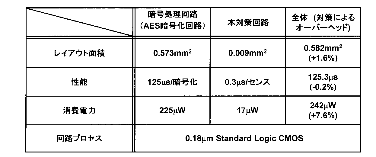
表1に、本発明に係るサイドチャネル攻撃の検知装置の機能と、暗号処理回路(1ラウンド/1クロックのループアーキテクチャに基づくAES暗号回路)に対する搭載時の面積、電力、性能オーバーヘッドを記載する。
本発明に係るサイドチャネル攻撃の検知装置(本対策回路)は、2.4%の面積と1%の電力と性能のわずかなオーバーヘッドで、従来の対策では防ぐことが困難な局所的な電磁波解析攻撃に対する耐性を実現できる。
本発明に係るサイドチャネル攻撃の検知装置(本対策回路)は、2.4%の面積と1%の電力と性能のわずかなオーバーヘッドで、従来の対策では防ぐことが困難な局所的な電磁波解析攻撃に対する耐性を実現できる。
また、本発明に係るサイドチャネル攻撃の検知装置は、ハイディングやマスキングなどの先行するサイドチャネル攻撃対策とも組み合わせ可能であり、相補的に組み合わせることにより、より堅牢なセキュリティを有する暗号処理回路を実現できる。
<本発明の他の実施形態>
上記実施形態に係るサイドチャネル攻撃の検知装置は、図2、図4などに示したように、検知手段としてコイル(インダクタ)を備えたLC発振器を採用し、導電体などにより構成されるプローブなどの接近によるインダクタンス(相互インダクタンス)の変化に応じた発振周波数の変化や、暗号処理回路などの情報処理装置を含むLSIのパッケージ(導電体や樹脂などにより構成される)の開封によるインダクタンス(相互インダクタンス)の変化に応じた発振周波数の変化に基づいて判定手段としての制御回路がサイドチャネル攻撃によるプローブの接近やLSIパッケージの開封などを判定したが、この形態に限られるものではない。
上記実施形態に係るサイドチャネル攻撃の検知装置は、図2、図4などに示したように、検知手段としてコイル(インダクタ)を備えたLC発振器を採用し、導電体などにより構成されるプローブなどの接近によるインダクタンス(相互インダクタンス)の変化に応じた発振周波数の変化や、暗号処理回路などの情報処理装置を含むLSIのパッケージ(導電体や樹脂などにより構成される)の開封によるインダクタンス(相互インダクタンス)の変化に応じた発振周波数の変化に基づいて判定手段としての制御回路がサイドチャネル攻撃によるプローブの接近やLSIパッケージの開封などを判定したが、この形態に限られるものではない。
例えば、本発明に係る検知装置は、プローブなどの接近によるキャパシタンス(相互キャパシタンス)の変化に基づいて、上述したように、プローブなどを検知する検知手段と、その検知手段の出力に基づいてサイドチャネル攻撃によるプローブの接近やLSIパッケージの開封などを判定する制御回路などの判定手段などを有してもよい。
図15は本発明の他の実施形態に係るサイドチャネル攻撃の検知装置の一例を説明するための概念図である。図16は伝達関数の一例を示す図である。詳細には、図16(a)はプローブが検知手段に接近していない場合の伝達関数の一例を示す図、図16(b)はプローブが検知手段に接近している場合の伝達関数の一例を示す図である。図17は入力信号の電圧の周波数特性の一例を示す図である。
例えば、図15に示した本発明に係る検知装置は、集積回路チップ10に形成された情報処理装置3の近傍に、検知手段として、導電体により細長の伝送路201を設けることによりキャパシタを形成し、その伝送路201の一方の端部から所定の信号(図17参照)を入力し、伝送路201の他方の端部で信号を受信し、その信号に基づいて判定手段としての制御回路5が伝達関数の変化によりプローブ7の接近を判定してもよい。つまり、図16に示した例では、検知手段による、プローブ7の接近による容量結合の変化(キャパシタンスの変化)を示す出力に基づいて、判定手段としての制御回路5がサイドチャネル攻撃によるプローブの接近を判定する。
また、上述した暗号処理回路などの情報処理装置を含むLSI(集積回路チップ10)が導電体や樹脂などにより構成されるLSIパッケージに収容されている場合、上記検知装置は、パッケージの開封による容量結合の変化(キャパシタンスの変化)に基づいてサイドチャネル攻撃を検知してもよい。詳細には、上述したように、集積回路チップ10に形成された情報処理装置3の近傍に、検知手段として、導電体などにより伝送路201を設けることによりキャパシタを形成し、その伝送路201の一方の端部から、所定の信号(図17参照)を入力し、伝送路201の他方の端部で信号を受信し、伝達関数の変化に基づいて判定手段としての制御回路5がLSIパッケージの開封を判定してもよい。つまり、検知手段により、パッケージの開封時の容量結合による容量結合の変化(キャパシタンスの変化)に基づいて、判定手段としての制御回路5がLSIパッケージの開封を判定する。
例えば、図15に示した本発明に係る検知装置は、集積回路チップ10に形成された情報処理装置3の近傍に、検知手段として、導電体により細長の伝送路201を設けることによりキャパシタを形成し、その伝送路201の一方の端部から所定の信号(図17参照)を入力し、伝送路201の他方の端部で信号を受信し、その信号に基づいて判定手段としての制御回路5が伝達関数の変化によりプローブ7の接近を判定してもよい。つまり、図16に示した例では、検知手段による、プローブ7の接近による容量結合の変化(キャパシタンスの変化)を示す出力に基づいて、判定手段としての制御回路5がサイドチャネル攻撃によるプローブの接近を判定する。
また、上述した暗号処理回路などの情報処理装置を含むLSI(集積回路チップ10)が導電体や樹脂などにより構成されるLSIパッケージに収容されている場合、上記検知装置は、パッケージの開封による容量結合の変化(キャパシタンスの変化)に基づいてサイドチャネル攻撃を検知してもよい。詳細には、上述したように、集積回路チップ10に形成された情報処理装置3の近傍に、検知手段として、導電体などにより伝送路201を設けることによりキャパシタを形成し、その伝送路201の一方の端部から、所定の信号(図17参照)を入力し、伝送路201の他方の端部で信号を受信し、伝達関数の変化に基づいて判定手段としての制御回路5がLSIパッケージの開封を判定してもよい。つまり、検知手段により、パッケージの開封時の容量結合による容量結合の変化(キャパシタンスの変化)に基づいて、判定手段としての制御回路5がLSIパッケージの開封を判定する。
以上、説明したように、本発明の実施形態に係るサイドチャネル攻撃の検知装置1は、サイドチャネル攻撃の対象となる情報処理装置に近接して配置されたコイル(インダクタ)またはキャパシタを有し、コイル(インダクタ)のインダクタンスまたはキャパシタのキャパシタンスの変化を検知する検知手段と、その検知手段によりサイドチャネル攻撃によるプローブの接近またはLSIパッケージの開封を判定する判定手段としての制御回路5と、を有する。
このため、簡単な構成で、サイドチャネル攻撃を検知可能な検知装置を提供することができる。
また、制御回路は、サイドチャネル攻撃によるプローブの接近またはLSIパッケージの開封を検知した場合、上述したように、暗号処理回路の秘密情報を保護する動作モードに切り替える処理を行ってもよい。
このため、簡単な構成で、サイドチャネル攻撃を検知可能な検知装置を提供することができる。
また、制御回路は、サイドチャネル攻撃によるプローブの接近またはLSIパッケージの開封を検知した場合、上述したように、暗号処理回路の秘密情報を保護する動作モードに切り替える処理を行ってもよい。
また、本発明に係る検知装置は、上記検知手段を有するので、従来対策では防ぐことが困難な局所電磁波解析攻撃も含めてプロービングによる電気的情報を用いるサイドチャネル攻撃全般を防ぐことができる。
また、本発明に係る検知装置は、集積回路内部やプリント基板上の配線パターンから放射される電磁界を測定するためにプローブを接近させると、コイルのインダクタンスの変化、詳細には、例えば、集積回路やプリント基板上の配線と(プローブを含む)周囲との電磁界結合度が変化し、不可避に電磁界分布に変化が生じるという物理法則に基づいて、サイドチャネル攻撃を検知することができ、攻撃者は原理的に検知されることなく攻撃を行うことは困難となる。
また、本発明では、従来対策に対して、暗号LSIの実行速度や消費電力、実装面積などのオーバーヘッドを大きく削減している。従来対策は少なくとも回路規模を数倍程度増加する。一方、本発明では、検知手段をLC発振器により構成した場合、対策対象となる暗号処理回路に対して2.4%というわずかな面積オーバーヘッドで実現できる。また、コイル以外のすべての回路は完全デジタル回路(ロジック回路)で構成できるので、集積回路製造プロセスの微細化に応じて、暗号コアと同様に面積を縮小できる。
また、コイルについても集積回路製造プロセスの微細化によるトランジスタ性能の改善により縮小可能であり、暗号コアに対するセンサ全体の面積オーバーヘッドについても一定に保つことが出来る。
また、コイルについても集積回路製造プロセスの微細化によるトランジスタ性能の改善により縮小可能であり、暗号コアに対するセンサ全体の面積オーバーヘッドについても一定に保つことが出来る。
また、本発明に係る検知装置は、検知手段をLC発振器により構成した場合、コイル以外の回路を完全デジタル回路(ロジック回路)で構成できるため、設計容易性が高く、集積回路製造プロセスの微細化に応じて、暗号コアと同様に面積を縮小できる。
また、本発明に係る検知装置は、形状・巻き数の異なる2つ以上のコイルを用いた攻撃検知方式により、多様なプロービング方法を検知可能にするとともに、高精度な周波数基準を不要にすることで周波数基準に対する攻撃も不可能にする。
また、本発明では、2コイル以上を用いた攻撃検知方式により高精度な周波数基準を不要にし、周波数基準に対する攻撃を不可能にするだけでなく、本発明による回路面積や消費電力の増加を大きく削減することに寄与する。さらに、リング発振器を用いたセンサのワンステップデジタル較正により、PVTばらつきにも対応可能である。
さらに、リング発振器を用いたLC発振器の発振周波数のワンステップデジタル較正により、様々な動作環境にも対応可能である。
本発明は、上記機能を実現した場合でも、対策対象となる暗号処理回路(情報処理装置)に対して、例えば、2.4%程度という僅かな面積オーバーヘッドで実現できる。
本発明は、上記機能を実現した場合でも、対策対象となる暗号処理回路(情報処理装置)に対して、例えば、2.4%程度という僅かな面積オーバーヘッドで実現できる。
また、本発明によれば、上記サイドチャネル攻撃の検知装置を有する半導体装置を提供することができる。
また、本発明によれば、上記サイドチャネル攻撃の検知装置によるサイドチャネル攻撃の検知方法を提供することができる。
また、本発明によれば、上記サイドチャネル攻撃の検知装置によるサイドチャネル攻撃の検知方法を提供することができる。
1…検知装置
2…検知手段
3…情報処理装置
3a…暗号処理回路
5…制御回路(判定手段:制御部)
7…プローブ
8L…LC発振器
8R…リング発振器
10…集積回路チップ
50…センサコア回路
55…較正回路
57,57a,57b…カウンタ
L,L1,L2…コイル。
2…検知手段
3…情報処理装置
3a…暗号処理回路
5…制御回路(判定手段:制御部)
7…プローブ
8L…LC発振器
8R…リング発振器
10…集積回路チップ
50…センサコア回路
55…較正回路
57,57a,57b…カウンタ
L,L1,L2…コイル。
Claims (14)
- サイドチャネル攻撃の対象となる情報処理装置に近接して配置されたインダクタを有し、前記インダクタのインダクタンスの変化を検知する検知手段と、
前記検知手段の出力に基づいて前記サイドチャネル攻撃によるプローブの接近またはLSIパッケージの開封を判定する判定手段と、を有することを特徴とする
サイドチャネル攻撃の検知装置。 - 前記検知手段は、前記インダクタを含む発振回路を有し、前記発振回路の発振周波数の変化を検知することを特徴とする請求項1に記載のサイドチャネル攻撃の検知装置。
- 前記検知手段の前記インダクタは複数であることを特徴とする請求項1または請求項2に記載のサイドチャネル攻撃の検知装置。
- 前記複数のインダクタは、それぞれ形状が異なることを特徴とする請求項3に記載のサイドチャネル攻撃の検知装置。
- 前記複数のインダクタは、それぞれ巻き数が異なることを特徴とする請求項3または請求項4に記載のサイドチャネル攻撃の検知装置。
- 前記検知手段は、前記インダクタを除きロジック回路で構成されていることを特徴とする請求項1から請求項5の何れかに記載のサイドチャネル攻撃の検知装置。
- リング発振回路を備え、該リング発振回路の発振周波数に基づいて、前記検知手段の前記発振回路のキャパシタンスを調整することで該発振回路の発振周波数を較正する手段を有することを特徴とする請求項2から請求項6の何れかに記載のサイドチャネル攻撃の検知装置。
- サイドチャネル攻撃の対象となる情報処理装置に近接して配置されたキャパシタを有し、前記キャパシタのキャパシタンスの変化を検知する検知手段と、
前記検知手段の出力に基づいて前記サイドチャネル攻撃によるプローブの接近またはLSIパッケージの開封を判定する判定手段と、を有することを特徴とする
サイドチャネル攻撃の検知装置。 - 前記サイドチャネル攻撃によるプローブの接近またはLSIパッケージの開封を検知した場合、暗号処理回路の秘密情報を保護する動作モードに切り替える制御回路を有することを特徴とする請求項1から請求項8の何れかに記載のサイドチャネル攻撃の検知装置。
- 前記制御回路は、少なくとも、暗号処理回路の暗号処理を停止させる処理、ダミー演算処理、ハイディング処理、マスキング処理のいずれかを含むことを特徴とする請求項9に記載のサイドチャネル攻撃の検知装置。
- 前記制御回路は、少なくとも、偽の鍵を用いた暗号処理、鍵の変更処理、暗号処理に関わる情報を消去する処理、検知したことを外部に通知する処理、のいずれかを含むことを特徴とする請求項9に記載のサイドチャネル攻撃の検知装置。
- 前記情報処理装置および前記検知手段は、同一の集積回路チップに設けられていることを特徴とする請求項1から請求項11の何れかに記載のサイドチャネル攻撃の検知装置。
- 請求項1から請求項12の何れかに記載のサイドチャネル攻撃の検知装置を有する半導体装置。
- 請求項1から請求項12の何れかに記載のサイドチャネル攻撃の検知装置によるサイドチャネル攻撃の検知方法。
Applications Claiming Priority (2)
| Application Number | Priority Date | Filing Date | Title |
|---|---|---|---|
| JP2014018033A JP2017079336A (ja) | 2014-01-31 | 2014-01-31 | サイドチャネル攻撃の検知装置、サイドチャネル攻撃の検知装置によるサイドチャネル攻撃の検知方法 |
| JP2014-018033 | 2014-01-31 |
Publications (1)
| Publication Number | Publication Date |
|---|---|
| WO2015114944A1 true WO2015114944A1 (ja) | 2015-08-06 |
Family
ID=53756538
Family Applications (1)
| Application Number | Title | Priority Date | Filing Date |
|---|---|---|---|
| PCT/JP2014/082010 Ceased WO2015114944A1 (ja) | 2014-01-31 | 2014-12-03 | サイドチャネル攻撃の検知装置、サイドチャネル攻撃の検知装置によるサイドチャネル攻撃の検知方法 |
Country Status (3)
| Country | Link |
|---|---|
| JP (1) | JP2017079336A (ja) |
| TW (1) | TW201541283A (ja) |
| WO (1) | WO2015114944A1 (ja) |
Cited By (3)
| Publication number | Priority date | Publication date | Assignee | Title |
|---|---|---|---|---|
| JP2019500575A (ja) * | 2015-09-25 | 2019-01-10 | クアルコム,インコーポレイテッド | プロセスコーナーを識別する技法 |
| CN113196478A (zh) * | 2018-12-26 | 2021-07-30 | 索尼半导体解决方案公司 | 电路板、半导体装置和电子设备 |
| EP3995977A1 (en) * | 2020-11-10 | 2022-05-11 | Thales DIS France SA | Method for detecting an attack on a sensitive unit of an electronic system |
Families Citing this family (6)
| Publication number | Priority date | Publication date | Assignee | Title |
|---|---|---|---|---|
| KR101879809B1 (ko) * | 2017-09-19 | 2018-08-16 | 국민대학교산학협력단 | 부채널 분석에 안전한 연산 장치 및 방법 |
| CN107942154A (zh) * | 2017-10-16 | 2018-04-20 | 北京中电华大电子设计有限责任公司 | 一种适用于芯片电磁攻击防护的保护结构和方法 |
| JP7248237B2 (ja) * | 2019-03-28 | 2023-03-29 | 株式会社Scu | システム半導体チップ、システム半導体チップの情報漏洩検出方法及びシステム半導体チップの情報漏洩抑止方法 |
| TWI785855B (zh) * | 2021-10-21 | 2022-12-01 | 中國鋼鐵股份有限公司 | 檢測裝置 |
| KR20230095686A (ko) | 2021-12-22 | 2023-06-29 | 삼성전자주식회사 | 악의적 공격 방지 회로, 이를 포함하는 시스템 온 칩, 및 그의 동작 방법 |
| US12277220B2 (en) | 2022-02-16 | 2025-04-15 | Nxp B.V. | Method and device for detecting a profiling attack |
Citations (2)
| Publication number | Priority date | Publication date | Assignee | Title |
|---|---|---|---|---|
| JPH0660234A (ja) * | 1991-11-27 | 1994-03-04 | Us Government | 電気的手段による非接触式タンパー検出 |
| JP2007535022A (ja) * | 2003-12-29 | 2007-11-29 | コミツサリア タ レネルジー アトミーク | 機密データを含む集積回路チップの保護 |
-
2014
- 2014-01-31 JP JP2014018033A patent/JP2017079336A/ja active Pending
- 2014-12-03 WO PCT/JP2014/082010 patent/WO2015114944A1/ja not_active Ceased
-
2015
- 2015-01-14 TW TW104101231A patent/TW201541283A/zh unknown
Patent Citations (2)
| Publication number | Priority date | Publication date | Assignee | Title |
|---|---|---|---|---|
| JPH0660234A (ja) * | 1991-11-27 | 1994-03-04 | Us Government | 電気的手段による非接触式タンパー検出 |
| JP2007535022A (ja) * | 2003-12-29 | 2007-11-29 | コミツサリア タ レネルジー アトミーク | 機密データを含む集積回路チップの保護 |
Cited By (4)
| Publication number | Priority date | Publication date | Assignee | Title |
|---|---|---|---|---|
| JP2019500575A (ja) * | 2015-09-25 | 2019-01-10 | クアルコム,インコーポレイテッド | プロセスコーナーを識別する技法 |
| CN113196478A (zh) * | 2018-12-26 | 2021-07-30 | 索尼半导体解决方案公司 | 电路板、半导体装置和电子设备 |
| EP3995977A1 (en) * | 2020-11-10 | 2022-05-11 | Thales DIS France SA | Method for detecting an attack on a sensitive unit of an electronic system |
| WO2022101223A1 (en) * | 2020-11-10 | 2022-05-19 | Thales Dis France Sas | Method for detecting an attack on a sensitive unit of an electronic system |
Also Published As
| Publication number | Publication date |
|---|---|
| JP2017079336A (ja) | 2017-04-27 |
| TW201541283A (zh) | 2015-11-01 |
Similar Documents
| Publication | Publication Date | Title |
|---|---|---|
| WO2015114944A1 (ja) | サイドチャネル攻撃の検知装置、サイドチャネル攻撃の検知装置によるサイドチャネル攻撃の検知方法 | |
| Standaert | Introduction to side-channel attacks | |
| CN105391542B (zh) | 用于集成电路检测电磁故障注入攻击探测方法及探测器 | |
| Homma et al. | Em attack is non-invasive?-design methodology and validity verification of em attack sensor | |
| Ordas et al. | Evidence of a larger EM-induced fault model | |
| Wang et al. | Novel physical unclonable function with process and environmental variations | |
| Homma et al. | Design methodology and validity verification for a reactive countermeasure against EM attacks | |
| CA2733667C (en) | Method for detecting abnormalities in a cryptographic circuit protected by differential logic, and circuit for implementing said method | |
| Tehranipoor et al. | Hardware security primitives | |
| Hettwer et al. | Deep learning multi-channel fusion attack against side-channel protected hardware | |
| Li et al. | Yet another fault-based leakage in non-uniform faulty ciphertexts | |
| Bhasin et al. | Fault Injection Attacks: Attack Methodologies, Injection Techniques and Protection Mechanisms: A Tutorial | |
| US20170373837A1 (en) | Protection method and device against a side-channel analysis | |
| JP5482048B2 (ja) | 集積回路および電子機器 | |
| Antonopoulos et al. | Hardware Trojans in analog, mixed-signal, and RF ICs | |
| Mohankumar et al. | Lightweight logic obfuscation in combinational circuits for improved security—An analysis | |
| Fujino et al. | Tamper-resistant cryptographic hardware | |
| Nozaki et al. | Power consumption aware machine learning attack for feed-forward arbiter PUF | |
| Druml et al. | Secured miniaturized system-in-package contactless and passive authentication devices featuring NFC | |
| Montminy | Enhancing Electromagnetic Side-Channel Analysis in an Operational Environment | |
| Das et al. | Security of analog, mixed-signal, and RF devices | |
| Mai | Side channel attacks and countermeasures | |
| Nagata et al. | Analog Techniques for Digital Security: My gratitudes to visionary discussions | |
| Gnad et al. | Remote physical attacks on fpgas at the electrical level | |
| Halak | Security attacks on physically unclonable functions and possible countermeasures |
Legal Events
| Date | Code | Title | Description |
|---|---|---|---|
| 121 | Ep: the epo has been informed by wipo that ep was designated in this application |
Ref document number: 14880675 Country of ref document: EP Kind code of ref document: A1 |
|
| NENP | Non-entry into the national phase |
Ref country code: DE |
|
| 122 | Ep: pct application non-entry in european phase |
Ref document number: 14880675 Country of ref document: EP Kind code of ref document: A1 |
|
| NENP | Non-entry into the national phase |
Ref country code: JP |