WO2015114754A1 - Dispositif à mémoire - Google Patents
Dispositif à mémoire Download PDFInfo
- Publication number
- WO2015114754A1 WO2015114754A1 PCT/JP2014/051949 JP2014051949W WO2015114754A1 WO 2015114754 A1 WO2015114754 A1 WO 2015114754A1 JP 2014051949 W JP2014051949 W JP 2014051949W WO 2015114754 A1 WO2015114754 A1 WO 2015114754A1
- Authority
- WO
- WIPO (PCT)
- Prior art keywords
- physical
- page
- flash memory
- logical
- data
- Prior art date
Links
Images


Classifications
-
- G—PHYSICS
- G06—COMPUTING; CALCULATING OR COUNTING
- G06F—ELECTRIC DIGITAL DATA PROCESSING
- G06F12/00—Accessing, addressing or allocating within memory systems or architectures
- G06F12/02—Addressing or allocation; Relocation
- G06F12/08—Addressing or allocation; Relocation in hierarchically structured memory systems, e.g. virtual memory systems
- G06F12/10—Address translation
- G06F12/1009—Address translation using page tables, e.g. page table structures
-
- G—PHYSICS
- G06—COMPUTING; CALCULATING OR COUNTING
- G06F—ELECTRIC DIGITAL DATA PROCESSING
- G06F12/00—Accessing, addressing or allocating within memory systems or architectures
- G06F12/02—Addressing or allocation; Relocation
- G06F12/0223—User address space allocation, e.g. contiguous or non contiguous base addressing
- G06F12/023—Free address space management
- G06F12/0238—Memory management in non-volatile memory, e.g. resistive RAM or ferroelectric memory
- G06F12/0246—Memory management in non-volatile memory, e.g. resistive RAM or ferroelectric memory in block erasable memory, e.g. flash memory
-
- G—PHYSICS
- G06—COMPUTING; CALCULATING OR COUNTING
- G06F—ELECTRIC DIGITAL DATA PROCESSING
- G06F3/00—Input arrangements for transferring data to be processed into a form capable of being handled by the computer; Output arrangements for transferring data from processing unit to output unit, e.g. interface arrangements
- G06F3/06—Digital input from, or digital output to, record carriers, e.g. RAID, emulated record carriers or networked record carriers
- G06F3/0601—Interfaces specially adapted for storage systems
- G06F3/0602—Interfaces specially adapted for storage systems specifically adapted to achieve a particular effect
- G06F3/061—Improving I/O performance
-
- G—PHYSICS
- G06—COMPUTING; CALCULATING OR COUNTING
- G06F—ELECTRIC DIGITAL DATA PROCESSING
- G06F3/00—Input arrangements for transferring data to be processed into a form capable of being handled by the computer; Output arrangements for transferring data from processing unit to output unit, e.g. interface arrangements
- G06F3/06—Digital input from, or digital output to, record carriers, e.g. RAID, emulated record carriers or networked record carriers
- G06F3/0601—Interfaces specially adapted for storage systems
- G06F3/0602—Interfaces specially adapted for storage systems specifically adapted to achieve a particular effect
- G06F3/0614—Improving the reliability of storage systems
- G06F3/0616—Improving the reliability of storage systems in relation to life time, e.g. increasing Mean Time Between Failures [MTBF]
-
- G—PHYSICS
- G06—COMPUTING; CALCULATING OR COUNTING
- G06F—ELECTRIC DIGITAL DATA PROCESSING
- G06F3/00—Input arrangements for transferring data to be processed into a form capable of being handled by the computer; Output arrangements for transferring data from processing unit to output unit, e.g. interface arrangements
- G06F3/06—Digital input from, or digital output to, record carriers, e.g. RAID, emulated record carriers or networked record carriers
- G06F3/0601—Interfaces specially adapted for storage systems
- G06F3/0628—Interfaces specially adapted for storage systems making use of a particular technique
- G06F3/0638—Organizing or formatting or addressing of data
- G06F3/064—Management of blocks
-
- G—PHYSICS
- G06—COMPUTING; CALCULATING OR COUNTING
- G06F—ELECTRIC DIGITAL DATA PROCESSING
- G06F3/00—Input arrangements for transferring data to be processed into a form capable of being handled by the computer; Output arrangements for transferring data from processing unit to output unit, e.g. interface arrangements
- G06F3/06—Digital input from, or digital output to, record carriers, e.g. RAID, emulated record carriers or networked record carriers
- G06F3/0601—Interfaces specially adapted for storage systems
- G06F3/0628—Interfaces specially adapted for storage systems making use of a particular technique
- G06F3/0638—Organizing or formatting or addressing of data
- G06F3/0644—Management of space entities, e.g. partitions, extents, pools
-
- G—PHYSICS
- G06—COMPUTING; CALCULATING OR COUNTING
- G06F—ELECTRIC DIGITAL DATA PROCESSING
- G06F3/00—Input arrangements for transferring data to be processed into a form capable of being handled by the computer; Output arrangements for transferring data from processing unit to output unit, e.g. interface arrangements
- G06F3/06—Digital input from, or digital output to, record carriers, e.g. RAID, emulated record carriers or networked record carriers
- G06F3/0601—Interfaces specially adapted for storage systems
- G06F3/0628—Interfaces specially adapted for storage systems making use of a particular technique
- G06F3/0655—Vertical data movement, i.e. input-output transfer; data movement between one or more hosts and one or more storage devices
- G06F3/0656—Data buffering arrangements
-
- G—PHYSICS
- G06—COMPUTING; CALCULATING OR COUNTING
- G06F—ELECTRIC DIGITAL DATA PROCESSING
- G06F3/00—Input arrangements for transferring data to be processed into a form capable of being handled by the computer; Output arrangements for transferring data from processing unit to output unit, e.g. interface arrangements
- G06F3/06—Digital input from, or digital output to, record carriers, e.g. RAID, emulated record carriers or networked record carriers
- G06F3/0601—Interfaces specially adapted for storage systems
- G06F3/0668—Interfaces specially adapted for storage systems adopting a particular infrastructure
- G06F3/0671—In-line storage system
- G06F3/0673—Single storage device
- G06F3/0679—Non-volatile semiconductor memory device, e.g. flash memory, one time programmable memory [OTP]
-
- G—PHYSICS
- G06—COMPUTING; CALCULATING OR COUNTING
- G06F—ELECTRIC DIGITAL DATA PROCESSING
- G06F3/00—Input arrangements for transferring data to be processed into a form capable of being handled by the computer; Output arrangements for transferring data from processing unit to output unit, e.g. interface arrangements
- G06F3/06—Digital input from, or digital output to, record carriers, e.g. RAID, emulated record carriers or networked record carriers
- G06F3/0601—Interfaces specially adapted for storage systems
- G06F3/0668—Interfaces specially adapted for storage systems adopting a particular infrastructure
- G06F3/0671—In-line storage system
- G06F3/0683—Plurality of storage devices
- G06F3/0688—Non-volatile semiconductor memory arrays
-
- G—PHYSICS
- G06—COMPUTING; CALCULATING OR COUNTING
- G06F—ELECTRIC DIGITAL DATA PROCESSING
- G06F2212/00—Indexing scheme relating to accessing, addressing or allocation within memory systems or architectures
- G06F2212/65—Details of virtual memory and virtual address translation
- G06F2212/657—Virtual address space management
-
- G—PHYSICS
- G06—COMPUTING; CALCULATING OR COUNTING
- G06F—ELECTRIC DIGITAL DATA PROCESSING
- G06F2212/00—Indexing scheme relating to accessing, addressing or allocation within memory systems or architectures
- G06F2212/72—Details relating to flash memory management
- G06F2212/7201—Logical to physical mapping or translation of blocks or pages
-
- G—PHYSICS
- G06—COMPUTING; CALCULATING OR COUNTING
- G06F—ELECTRIC DIGITAL DATA PROCESSING
- G06F2212/00—Indexing scheme relating to accessing, addressing or allocation within memory systems or architectures
- G06F2212/72—Details relating to flash memory management
- G06F2212/7204—Capacity control, e.g. partitioning, end-of-life degradation
Definitions
- the present invention relates to a storage apparatus using a nonvolatile semiconductor memory and a control method thereof.
- Nonvolatile semiconductor memory has higher power consumption, higher performance and higher price than magnetic storage devices.
- Such a nonvolatile semiconductor memory is, for example, a NAND flash memory.
- the price has been reduced, and it has been attracting attention as a mainstream storage device replacing HDD.
- a block is a data erasing unit
- a page is a storage area for reading / writing data.
- block / page simply refers to a flash memory.
- flash memory cannot directly rewrite stored data due to its characteristics. In other words, when rewriting stored data, the flash memory saves the stored valid data to another block.
- the flash memory erases the stored data in units of blocks. Then, the flash memory writes data to the erased block. As described above, rewriting of data in the flash memory is accompanied by erasure of data for each block.
- the time required for erasing data for one block in the flash memory is about one digit longer than the time required for writing data for one page. Therefore, if one block of data is erased each time for rewriting one page of data, the data rewriting performance of the flash memory is degraded. In order to cope with such a problem, it is known to write data into the flash memory using an algorithm that conceals the time to erase the data from the flash memory.
- the flash memory has a read error rate that increases with time even for pages that have been written once.
- An error that occurs just by holding in this way is called a retention error.
- a process is known in which a page that has passed for a certain period of time after writing is copied to another page. This process is called refresh. In some cases, it is abbreviated as RF. Also in the refresh, it is necessary to consider the leveling problem and performance influence already described.
- the flash storage performs a logical physical address conversion process for converting a logical address to a physical address when writing data.
- the flash memory module includes one or more flash memory chips and a flash memory controller that controls reading and writing of data with respect to the flash memory chips. This flash memory controller performs logical-physical address conversion processing. Further, the flash memory controller stores information for logical physical address conversion processing as a logical physical address conversion table.
- the logical / physical address conversion process may be referred to as logical / physical conversion
- the logical / physical address conversion table may be referred to as logical / physical conversion table.
- the logical-physical conversion has an important role in using the flash memory efficiently.
- a logical-physical conversion with a low degree of freedom When a logical-physical conversion with a low degree of freedom is used, the performance deteriorates due to frequent reclamation instead of suppressing the size of the logical-physical conversion table.
- the size of the logical-physical conversion table becomes enormous, and the control cost greatly increases.
- the address space provided to the host device is divided by the page size of the flash memory.
- This logical unit may be called a logical page, and a page of the flash memory may be called a physical page to distinguish it.
- the final size varies due to data conversion processing such as compression. Reducing the bit cost of flash memory is a major goal for the replacement of HDD, and data compression is widely applied to flash storage.
- the characteristics of flash memory are not uniform for all physical pages, there are innate differences and there are differences depending on physical locations. Therefore, instead of using the same ECC for all physical pages, it may be possible to adopt an optimal storage method according to the situation. In that case, the size mismatch between the logical page and the physical page becomes more prominent.
- a flash memory storage device includes a controller and a plurality of flash memory chips.
- the controller divides and manages the logical storage space provided to the host device in units of logical pages, which are areas of a predetermined size, and is a linear in which a plurality of physical blocks of a plurality of flash memory chips are associated with each other. It has a virtual address space which is an address space.
- the unused area on the virtual address space is selected, and the correspondence between the address of the unused area on the selected virtual address space and the logical page is displayed on the page. Record in the mapping table.
- any area can be selected as long as it is an unused area, and there is no need to be aware of physical page boundaries.
- a storage device having a write unit data in a logical management unit different from the write unit can be stored across the write unit boundary, and the storage efficiency is improved. Further, even if the data of the logical management unit is stored across the writing unit boundary, the information on the storage location of the logical management unit data on the storage device can be managed without increasing the size of the management information.
- FIG. 1 shows a configuration diagram of a storage system.
- FIG. 2 shows a configuration diagram of FMPKG.
- FIG. 3 shows the contents of the main memory of the flash memory storage.
- FIG. 4 shows the relationship between the block and page of the flash memory.
- FIG. 5 shows a general data storage configuration in a physical page.
- FIG. 6 shows an outline of a page-based logical-physical conversion process performed in a conventional flash storage.
- FIG. 7 shows a page-based logical / physical conversion table.
- FIG. 8 shows a storage mode when the logical page size and the physical page size do not match.
- FIG. 9 shows a storage mode when one logical page extends over a plurality of physical pages.
- FIG. 10 is a diagram illustrating the concept of logical-physical conversion performed by FMPKG according to the first embodiment of the present invention.
- FIG. 11 shows the configuration of the page mapping table.
- FIG. 12 shows the configuration of the virtual address configuration information.
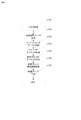
- FIG. 13 shows a flow of forward lookup processing in FMPKG according to Embodiment 1 of the present invention.
- FIG. 14 shows a flow of write processing in FMPKG according to the first embodiment of the present invention.
- FIG. 15 shows a flow of new group construction processing in FMPKG according to the first embodiment of the present invention.
- FIG. 16 shows a flow of RC / RF processing in FMPKG according to the first embodiment of the present invention.
- FIG. 17 shows the configuration of the page mapping table in Embodiment 2 of the present invention.
- FIG. 11 shows the configuration of the page mapping table.
- FIG. 12 shows the configuration of the virtual address configuration information.
- FIG. 13 shows a flow of forward lookup processing in FMPKG according to Embodiment 1
- FIG. 18 shows a flow of forward lookup processing in FMPKG according to the second embodiment of the present invention.
- FIG. 19 shows a flow of write processing in FMPKG according to the second embodiment of the present invention.
- FIG. 20 shows a flow of RC / RF processing in FMPKG according to the second embodiment of the present invention.
- FIG. 21 shows an example in which a virtual address group is configured with devices in which blocks having different physical page sizes exist.
- FIG. 22 shows a configuration of virtual address configuration information in FMPKG according to the third embodiment of the present invention.
- FIG. 23 shows a flow of forward lookup processing in FMPKG according to the third embodiment of the present invention.
- FIG. 24 shows a flow of new group construction processing in FMPKG according to the third embodiment of the present invention.
- program is used as the subject.
- the program performs processing defined by being executed by the processor using the memory and the communication port, this is actually the operation of the processor. It represents that a predetermined process is being executed as a subject. Further, part or all of the program may be realized by dedicated hardware.
- the various programs described in the present specification may be provided by a program distribution server or a storage medium that can be read by a computer.
- the nonvolatile memory in the following embodiments is FM (Flash Memory).
- the FM in this embodiment is a type of FM that is erased in units of blocks and read and written in units of pages, typically a NAND flash memory.
- the FM may be another type of flash memory (for example, NOR type) instead of the NAND type.
- other types of nonvolatile memory for example, MRAM (Magnetic Resistive Random Access Memory) which is a magnetoresistive memory, ReRAM (Resistance Random Access Memory) which is a resistance change type memory, and a ferroelectric memory.
- MRAM Magnetic Resistive Random Access Memory
- ReRAM Resistance Random Access Memory
- a semiconductor memory such as FeRAM (Ferroelectric Random Access Memory) or a phase change memory may be used.
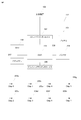
- FIG. 1 shows the configuration of a computer system related to Example 1 of the present invention.
- the computer system includes a storage system (storage device) 101, one or more host computers (abbreviated as “host” in the drawing) 103, and a management terminal 104.
- a storage system storage device
- host host computers
- management terminal 104 Each of the host computers 103 a and 103 b is connected to the storage system 101 via a SAN (Storage Area Network) 105.
- SAN Storage Area Network
- the storage system 101 includes a storage controller 102 and a plurality of flash memory storage devices 112 that are nonvolatile memory storage devices.
- the flash memory storage device may be referred to as FMPKG (Flash Memory Package).
- FMPKG Flash Memory Package
- the storage controller 102 includes a CPU (Central Processing Unit) 108, a memory 109, a plurality of host interfaces (hereinafter abbreviated as “host IF”) 107, and a plurality of drive interfaces (hereinafter abbreviated as “drive IF”). 110 and a maintenance interface (hereinafter abbreviated as “maintenance IF”) 106.
- Each unit in the storage controller 102 is connected via a bus.
- the memory 109 has an area for storing a program for controlling the storage system 101 and an area as a cache memory for temporarily storing data.
- the CPU 108 controls the storage system 101 according to a program stored in the memory 109.
- the host IF 107 is an interface for performing communication with the computer 103.
- the drive IF 110 is an interface for performing communication between the storage controller 102 and the FMPKG 112.
- the maintenance IF 106 is an interface that is connected to the management terminal 104 and communicates with the management terminal 104.
- the administrator performs management and maintenance of the storage controller 102 from the management terminal 104.
- the management terminal 104 is not an essential element, and the storage controller 102 can be managed and maintained from the host computer 103, for example.
- the host computer 103 and the FMPKG 112 are connected via the storage controller 102.
- the storage controller 102 may be omitted and the host computer 103 and the FMPKG 112 may be directly connected.
- FIG. 2 shows the configuration of the FMPKG 112.
- the FMPKG 112 includes a flash memory control device 201 and one or more flash memory chips (also referred to as FM chips. Also referred to as “FM Chip” in the drawing) 209a-h. As described above, other types of nonvolatile memory elements can be used instead of the FM chip.
- the flash memory control device 201 like the storage controller 102 or the host computer 103 in FIG. 1, issues a data access request to the FMPKG 112 (hereinafter, the storage controller 102 or the host computer 103 is referred to as “upper device 102”. And the FMPKG 112 are connected to the storage interface 202, the ASIC 203, the buffer 204, the battery 205 that supplies power in an emergency, the CPU 206, the main memory 207, and the flash memory interface 208 that connects to the flash memory.
- the FMPKG 112 are connected to the storage interface 202, the ASIC 203, the buffer 204, the battery 205 that supplies power in an emergency, the CPU 206, the main memory 207, and the flash memory interface 208 that connects to the flash memory.
- the CPU 206 is a processor that controls the entire flash memory control device 201, and operates based on a microprogram stored in the main memory 207.
- the logical memory conversion table stored in the main memory 207 is referred to read / write data from / to the flash memory chip 209. Also, reclamation and wear leveling are implemented according to the usage status of the flash memory.
- the ASIC 203 is controlled by the CPU 206 and reads / writes data from / to the flash memory chip 209. Similarly to the flash memory chip 209, communication with the host device is controlled through the storage interface 202.
- the CPU 206 is externally attached to the ASIC 203, but the ASIC 203 may be configured by a single LSI including the CPU 206, the storage interface 202, and the flash memory interface 208.
- the main memory 207 and the buffer 204 are volatile storage areas that can be accessed at higher speed, and are, for example, DRAMs.
- the main memory 207 is a work space used directly by the CPU 206 for control, and provides a shorter latency than the buffer 204.
- the buffer 204 stores a user data buffer or a large size table that cannot be stored in the main memory 207.
- main memory 207 and the buffer 204 are separated components, but they may be realized by one storage element.
- the storage interface 202 connects the host device and the flash memory control device 201 to perform communication.
- a storage interface such as SATA, SAS, or FC may be employed as this interface, or an interface such as PCI-Express may be employed.
- the internal architecture of the flash memory control device 201 is not necessarily as shown in the figure, and each function may be substituted by one or a plurality of devices.
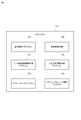
- FIG. 3 shows an example of information stored in the main memory 207 of the FMPKG 112.
- the main memory 207 stores, for example, an operating system 303, a flash storage control program 302, a data transfer control unit control program 301, an input / output control unit control program 304, a logical / physical conversion program 306, and a logical / physical conversion information 305.
- the operating system 303 is a program that performs basic processing such as scheduling when the CPU 206 executes each program.
- the flash storage control program 302 is a control for the flash memory control device 201 to operate as a storage device, such as management of a volume (or storage space of a volume) provided by the flash memory control device 201 to a host device, and management of a buffer memory. It is a program used for.
- the data transfer control unit control program 301 is a program used for controlling the ASIC 203.
- the input / output control unit control program 304 is a program used for controlling the storage interface 202 and the flash memory interface 208.
- the logical-physical conversion program 306 is a program that converts a logical address included in an input / output request (I / O request) issued from the host device 102 into a physical address that is a physical location on the flash memory.
- the “logical address” referred to in the present embodiment may be, for example, LBA (Logical Block Address).
- the “physical address” is an address (page number, block number) that uniquely identifies a physical page and / or physical block in the FMPKG 112, for example.
- the logical / physical conversion information 305 is information for conversion used when the logical / physical conversion program 306 operates.
- FIG. 4 shows the internal configuration of the flash memory chip 209.
- the flash memory chip 209 includes a plurality of dies (DIE) 401a to 401b and page buffers 402a to 402b for temporarily storing target data of a flash memory I / O command issued from the flash memory control device 201.
- Each die 401 has one or more (for example, 128, 256, etc.) physical blocks 403a to 403c which are actual storage areas.
- the physical block 403 is an erase unit in the flash memory.
- the physical block 403 is composed of one or more physical pages 404a to 404c.
- a physical page is a unit of writing / reading in the flash memory.
- Writing is writing of data to an erased physical page
- reading is reading of data written to the physical page.
- writing cannot be performed again on a physical page where writing has been performed, and when writing is performed again on a physical page, it is necessary to perform erasure once for each physical block 403 including the physical page. .
- the data stored in the physical page 404 included in the physical block 403 is erased and can be written again. It is not possible to erase only one physical page.
- Commands such as writing, reading, and erasing are received from a flash memory interface 208 that connects the flash memory chip 209 and the flash memory control device 201.
- FIG. 5 shows a general data storage configuration in the physical page 404.
- Code Word (CW) 501 is a set of data 502 and ECC 503 that protects the data 502, and is an error correction unit. There are one or more CWs in a physical page.
- a physical page holds a surplus area in addition to an area corresponding to the power of 2 to the number of bytes, and ECC and meta information are stored in this surplus area.
- ECC size is determined according to the reliability level required for the chip, the data area size for the power of 2 may not always be secured in one physical page.
- the term “physical page size” refers to the size of an area for storing user data that does not include an area for storing ECC or meta information from the size of the physical page of the original FM.
- FIG. 6 shows an overview of a page-based logical-physical conversion process performed in a conventional flash storage.
- An element 600 in the figure represents a storage space of a volume provided by the flash storage to the host device, and each sector (in the diagram, which is a minimum access unit when the host device accesses the storage area of the flash storage).
- Element 601) is assigned an address starting from 0, and this address is called a logical block address (LBA).
- LBA logical block address
- the size of one sector is 512 bytes, but other sizes (for example, 520 bytes) may be used.
- the flash storage divides the storage space provided by the flash storage to the host device into a predetermined size (for example, 16 sectors in the example shown in FIG. 6) from the top, and divides each divided area into “logical pages” ( It is managed as element 602) in the figure.
- page Y (604) in block X (603) represents a physical page.
- the sizes of all logical pages 602 and all physical pages 604 are fixed sizes (in the case of FIG. 6, 16 sectors, that is, 8 KB), and the logical pages 602 and physical pages 604 are equal in size. Therefore, one logical page 602 is uniquely associated with any one physical page 604, and information about the correspondence is managed in the logical-physical conversion table 701.
- a new unused physical page 604 is acquired, the update data of the logical page 602 is written to the unused physical page 604, and the association is updated.
- the old physical page 604 dereferenced from the logical page 602 is registered as an invalid page, collected / erased by reclamation, and reused as a free page.
- FIG. 7 shows an example of the configuration of a logical-physical conversion table 701 for page-based logical-physical conversion.
- This table is a table that a conventional flash storage normally has.
- the logical-physical conversion table 701 is a table that manages the address of the physical page 604 corresponding to each logical page 602.
- the logical page number (702) of each logical page 602 is associated with the logical page 602 of the logical page number 702.
- the address (storage address) 703 of the physical page 604 being stored is held. For example, when the flash storage provides a storage space with a size corresponding to N logical pages to the host device, there are N entries. When the storage destination of the logical page 602 is changed to a different physical page 604, the information of the storage address 703 in this table is updated.
- Case 1 in FIG. 8 shows an example where the logical page size is 1 ⁇ 2 of the physical page size
- Case 2 shows an example where the logical page size is larger than 1 ⁇ 2 of the physical page size.
- the logical page size is 1 ⁇ 2 of the physical page size, as in Case 1 of FIG. 8, or if the size is one power of 2 such as 1 ⁇ 4, 8, one physical page Several logical pages are just stored inside. Therefore, if the logical page size is a size that is a power of 2 of the physical page size, the physical page is divided into areas having the same size as the logical page size (this is called a “slot”) and managed.
- the logical / physical management table described with reference to FIG. 7 can be dealt with only by changing the correspondence between the logical page number of each logical page and the slot on the physical page.
- FIG. 9 shows a data storage configuration when one logical page is stored across a plurality of physical pages.
- the logical page may fit within one physical page (in the case of the logical page 901 in FIG. 9) or may be stored across two or more physical pages (in the case of the logical page 902 in FIG. 9). There is also.
- the size of each logical page is the same, and the size of each physical page is also the same.
- the size of the logical page and the size of the physical page do not match (even if the size of the logical page and the size of the physical page match), the FMPKG 112 described in the embodiment of the present invention can operate.
- the following description is based on the assumption that the logical page size and the physical page size do not match).
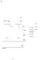
- FIG. 10 shows the concept of logical-physical conversion performed by the FMPKG 112.
- the logical-physical conversion performed by the FMPKG 112 is a concept in which the concept of virtual address space is incorporated into the concept of page-based logical-physical conversion described with reference to FIGS.
- the FMPKG 112 is a one-dimensional logical storage space (600 in FIG. 6) addressed to the host device by a logical block address (LBA) starting from address 0.
- LBA logical block address
- the one-dimensional logical space is divided into predetermined sizes (for example, 16 sectors) from the top, and each divided area is managed as a logical page.
- the area from address 0 to address 15 of the logical block address (LBA) in the one-dimensional logical storage space is associated with the logical page 1001a having the logical page number (LP) 0, and the one-dimensional logical storage is sequentially performed in the following order.
- the area where the LBA of the space is 16 to 31 is the logical page 1001b where the logical page number (LP) is 1, and the area where the LBA of the one-dimensional logical storage space is 32 to 47 is the logical page number (LP ) Is associated with the second logical page.
- the FMPKG 112 updates in units of logical pages (even if a write request for data having a size smaller than the logical page is received, the entire logical page including the data is updated. Therefore, it is preferable to select a data size (for example, 4 KB or 8 KB) specified by an I / O request issued by an OS, a file system, or an application program running on the host computer 103, for example.
- a data size for example, 4 KB or 8 KB
- the FMPKG 112 does not directly manage the correspondence between logical pages and physical pages, and each logical page (1001a, 1001b,...) Is a one-dimensional address space used only within the FMPKG 112. Are associated with addresses on the virtual address space 1003.
- Information about the correspondence between the logical page and the address on the virtual address space 1003 is managed using a page mapping table 1002 (FIG. 11) described later.
- the virtual address space 1003 is a one-dimensional linear address space that is not conscious of physical page boundaries, and the FMPKG 112 manages information constituting the virtual address space 1003 using virtual address configuration information 1007 (FIG. 12) described later. is doing.
- the virtual address space 1003 is an address space that does not make the physical page boundary conscious.
- a logical page is associated with the virtual address space 1003
- consideration is given to associating the logical page so as not to be stored across the physical page.
- the logical page may simply be associated with an arbitrary free area on the virtual address space (an area on the virtual address space to which the logical page is not yet associated).
- the virtual address space 1003 is not limited to a mode defined in the FMPKG 112, and a plurality of virtual address spaces 1003 may exist.
- each virtual address space is referred to as a virtual address group 1004 (hereinafter, a virtual address group may be simply referred to as a group).
- One virtual address configuration information 1007 is associated with each group.
- each logical page may be associated with an address of any group.
- the virtual address space 1003 is divided into the same size as the FM physical block 1008, and each divided area is called a “virtual block 1006”.
- Each virtual block 1006 is assigned an identification number (referred to as a virtual block number) that is unique within the virtual address group 1004.
- the first virtual block (1006a in FIG. 10) in the virtual address group 1004 is assigned a virtual block number 0, and the second and subsequent areas are sequentially numbered 1st, 2nd, and so on. A block number is assigned.
- each virtual block 1006 is mapped 1: 1 to the physical block 1008 on FM (corresponding to 403 in FIG. 4).
- This mapping information is managed in the virtual address configuration information 1007.
- a plurality of physical blocks are mapped in the virtual address space 1003.
- the information that the physical pages 1009a and 1009b in FIG. 10 are constituents of the same virtual address space is held not in units of pages but in units of blocks.
- management information can be greatly reduced.
- data of one logical page is not allowed to be stored across groups, an area in which user data is not stored is generated near the final address of the group in order to match the boundary. These areas may be invalid areas or may be used as areas for storing some management information.
- FIG. 11 illustrates the configuration of the page mapping table 1002 managed by the FMPKG 112 according to the first embodiment.
- the page mapping table 1002 is a table defined in one FMPKG 112, and correspondence between logical pages and addresses on the virtual address space 1003 (hereinafter, addresses in the virtual address space are referred to as “virtual addresses”). It is to manage the date.
- the page mapping table 1002 is one piece of information constituting the logical / physical conversion information 305 in the main memory 207.
- a virtual address set for each logical page includes a virtual address group number (group #) 1102 and an offset address 1103 within the group.
- the offset address 1103 stores a relative address where the address of the first sector of the group specified by the group # 1102 is 0.
- the FMPKG 112 determines an unwritten area address (group number and intra-group offset address) on the virtual address space to be associated with the logical page, and determines the group # 1102 and offset address. A value is stored in 1103. Similarly, when the data on the logical page is updated (overwritten), the address (group number and offset address within the group) of the unwritten area in the virtual address space is determined, and the group # 1102 and the offset address 1103 are assigned. Stores a value.
- the unit of the offset address 1103 is a sector, but other units may be used.
- an address with the size of one logical page as one unit may be stored in the offset address 1103.
- the page mapping table 1002 has only the same number of rows (entries) as the number of logical pages managed by the FMPKG 112.
- FIG. 12 shows the configuration of the virtual address configuration information 1007 managed by the FMPKG 112 according to the first embodiment. This information is also one piece of information constituting the logical / physical conversion information 305 of the main memory 207, as in the page mapping table 1002.
- the virtual address configuration information 1007 includes a next write position 1202 which is a pointer for holding the next write position for each virtual address group (group 1201) (in the embodiment of the present invention, the unit is a sector, And a physical block number (physical block #) 1204 of a plurality of physical blocks constituting the virtual address space of the corresponding group.
- group 1201 in the embodiment of the present invention, the unit is a sector
- physical block number (physical block #) 1204 of a plurality of physical blocks constituting the virtual address space of the corresponding group in the FMPKG 112 according to the embodiment of the present invention, each physical block in the FMPKG is managed with a unique identification number in the FMPKG, and this identification number is referred to as a physical block number.
- the physical block number 1204 stores this physical block number.
- N physical block numbers 1204 are registered in one group, and the physical block number registered at the top of each group is associated with the virtual block number (1203) of number 0, and thereafter Each physical block is associated with a virtual block number (1203) of No. 1, No. 2,.
- the size of the address space in the virtual address group is determined by the size of the number N of physical blocks constituting the virtual address group.
- the next write position 1202 is information indicating the start unwritten position of the corresponding virtual address group 1201.
- the write data from the higher-level device 102 is written to the virtual address group (the physical block / physical page associated with the virtual address group)
- the virtual address group the physical block / physical page associated with the virtual address group
- the data is written sequentially from the unwritten first page in the physical block (for example, if no data is written to the physical block, the first The page is the page of page number 0, and writing is performed in order on pages 1, 2,.
- the virtual address space specified by the address before the next write position 1202 means that the data has already been stored and mapped to the logical page, and is specified by the address after the next write position 1202.
- the space represents an unused area, that is, an area where data has not been written yet and is not mapped to a logical page.
- the value of the next write position 1202 is 0.
- the value n sectors is written by the write process, for example, the value n is added to the next write position 1202.
- a value of 0 or more (that is, a value that is not N / A is stored) is stored in the next write position 1202, and there is one group that can be written. There is only one.
- the group is referred to as “open group” or “open group”.
- a new group is constructed.
- the physical block (plural) constituting the group is selected, and the physical block number is stored in the physical block number 1204 column.
- a plurality of open groups may be provided, and an arbitrary open group may be selected and written when the FMPKG 112 writes data to a physical page.
- the virtual address configuration information 1007 information on the number of invalid pages 1205 and the last write time 1206 is held for each group.
- the number of invalid pages 1205 stores the number of pages that have become invalid due to data rewriting among the physical pages in the group, and at the last write time 1206, data was last written to the group. Stores the time.
- These pieces of information are used in reclamation (sometimes abbreviated as RC in this specification) or refresh (sometimes abbreviated as RF in this specification) processing.
- these pieces of information are managed for each group, but may be managed in other units such as for each physical block. For purposes such as RC and RF processing, information other than the number of invalid pages 1205 and the last write time 1206 may be managed.
- forward lookup process s1301 when the flash storage control program 302 executed by the CPU 206 receives an access request such as a read request from a higher-level device, for example, the physical storage location (physical page of the data to be accessed by the access request) ) Is performed.
- the flash storage control program 302 calls the logical-physical conversion program 306 and causes the CPU 206 to execute the forward lookup process s1301.
- the logical-physical translation program 306 calculates the physical address information (as a result of the forward lookup process s1301) ( A combination of the physical block number and the physical page number in the physical block specified by the physical block number) is returned to the flash storage control program 302 that is the request source.
- the start position of the access target data specified by the read request matches the logical page boundary and the size of the access target data is equal to one logical page size, that is, the physical position of the area for one logical page
- the physical storage position of the access target data can be calculated by performing the same process in other cases.
- the CPU 206 calculates the logical page number of the logical page to be accessed from the address (LBA) information of the access target data included in the processing target command (s1302). This is calculated by dividing the LBA of the access target data by the logical page size. Subsequently, the CPU 206 refers to the page mapping table 1002 to identify a row (entry) in which the logical page 1101 matches the logical page number calculated in s1302 (s1303), the group number 1102 of the row, The offset address 1103 is acquired (s1304).
- LBA address
- the CPU 206 refers to the page mapping table 1002 to identify a row (entry) in which the logical page 1101 matches the logical page number calculated in s1302 (s1303), the group number 1102 of the row, The offset address 1103 is acquired (s1304).
- the CPU 206 calculates the virtual block number and the offset address in the virtual block (relative address with the address of the start position of the virtual block being 0) from the offset address 1103 acquired in s1304 (s1305).
- the offset address 1103 obtained in s1304 is divided by the physical block size (the size of one physical page ⁇ the number of pages in one physical block), the quotient at this time is used as the virtual block number, and the remainder is stored in the virtual block. Use offset address.
- the CPU 206 refers to the virtual address configuration information 1007, refers to the row in which the group 1201 is equal to the group number acquired in s1304 and the virtual block number 1203 is equal to the virtual block number calculated in s1305, and the corresponding physical A block number (physical block # 1204) is acquired. It can be seen that the access target data exists in the physical block specified by the physical block number acquired in s1306.
- the CPU 206 divides the offset address in the virtual block calculated in s1305 by the physical page size, so that the relative page number in the physical block specified by the physical block number acquired in s1306 (the number of the first page in the physical block). And the physical page number of the physical page corresponding to the address included in the access request from the higher-level device (the first physical page storing the access target data) is calculated.
- the logical block offset address calculated in s1305 is “logical page size ⁇ 1”.
- the request source that has received the physical address performs processing such as reading the data from the physical page corresponding to the received physical address and returning it to the host device, for example, if the processing performed by the request source is read processing. .
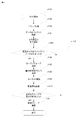
- the flow of processing in which the FMPKG 112 stores the write data from the higher-level device 102 in the physical page of the FM chip will be described. If it is assumed that write data is written in units of logical pages, an outline of the flow of write processing is as follows.
- the FMPKG 112 uses the virtual address configuration information 1007 to address the address (group number and group internal) of an unwritten area (an area in the virtual address space to which no logical page is yet associated). (Offset address) is determined, and the address information of the determined area is registered in the group 1102 and offset address 1103 fields of the page mapping table. Then, one or a plurality of physical pages corresponding to the determined unwritten area address may be specified, and write data may be stored in the specified physical page.
- write data can be stored in a physical page in units of logical pages.
- the minimum unit for writing data to the FM chip is a page (physical page)
- an invalid area may occur in the physical page in the above processing.
- data of a plurality of logical pages is accumulated in the buffer 204 in the FMPKG 112 so as not to generate an invalid area in the physical page, and then written to one or a plurality of physical pages collectively. Therefore, the processing is performed in a slightly different order from the above description.
- the flow of the write process s1401 that is executed when the FMPKG 112 receives a write request from the upper apparatus 102 will be described with reference to FIG.
- This process is realized by the CPU 206 executing the flash storage control program 302 and the logical / physical conversion program 306 in the main memory 207.
- a write request for data in which the start address and the end address of the write target data match the page boundary of the logical page is received from the host apparatus 102.
- Write command processing s1401 is processing for a write request from a higher-level device.
- the CPU 206 acquires a write command in s1402.
- the write command acquired in s1402 includes the write data storage position (write address, usually LBA is specified) and the write data length (number of sectors).
- the CPU 206 stores the write data in the buffer 204.
- the logical page number of the logical page in which the write data is stored is calculated from the write address and the write data length (in the case where the write data length is a length of a plurality of pages, the logical page number derived by conversion)
- the write data is stored in the buffer together with the logical page number derived by this conversion process.
- the CPU 206 confirms whether or not a certain amount of data exists on the buffer 204, and if it exists, performs processing to write the data on the buffer 204 to the physical page of the FM.
- a logical page is allowed to be stored across a plurality of physical pages.
- the minimum writing unit of FM is a physical page. Therefore, when writing to the FM in logical page units or physical page units, the entire logical page or fragment is written only in a part of the physical page, and the other area of the physical page becomes an invalid area. Occurs.
- a certain amount of data is collectively written in the FM.
- writing to the FM is performed (for example, the logical page size is 8 KB, the physical page size [as described above]
- “physical page size” is the size of the area in which data arriving from the host device is written excluding additional information such as ECC] is 7 KB, 56 KB or 56 KB which is the least common multiple of 8 and 7
- the CPU 206 acquires the group number of the open group.
- An open group means a group that is writable as described above.
- the CPU 206 calculates the physical block number 1204 and the intra-physical page number of the write destination physical block based on the next write position 1202 and the amount of data written to the current FM in the acquired open group. This is a method of calculating the physical block number 1204 and the page number in the physical block. By dividing the next write position 1202 by “the number of physical pages in one physical block ⁇ the physical page size (the unit of physical page size is the number of sectors)”.
- the virtual block number of the first physical block that is the data write target can be calculated, and the physical block number 1204 corresponding to the calculated virtual block number can be specified by referring to the virtual address configuration information 1007. Also, by calculating the remainder when the next write position 1202 is divided by “the number of physical pages in one physical block ⁇ the physical page size”, the first page number (first physical page number) of the page in the physical block that is the current write destination Can be obtained. Further, when the amount of data to be written to the FM this time spans multiple physical pages, page numbers corresponding to the required number of physical pages are acquired in sequence (it is necessary to acquire five physical pages and this write destination If the first physical page number of the page in the physical block is 3, the page numbers of page numbers 3, 4, 5, 6, and 7 are acquired).
- the CPU 206 sequentially writes the data on the buffer to the physical page specified by the physical address (physical block number 1204 of the write destination physical block and the page number in the physical block) acquired in s1407.
- the data for a plurality of logical pages on the buffer is continuously written to the physical page so that an invalid area does not occur (for example, as shown in FIG. 9).
- an address (group number, intra-group offset address) on the virtual address space corresponding to the physical page position where the data is stored is calculated (the physical page in which the data is stored).
- the writing to the physical page in the flash chip in s1408 is performed asynchronously with respect to the write request from the host device, and that a certain amount of data is collectively written to the physical page.
- This is effective for efficient and easy management when it is assumed that the physical page is a writing unit and the logical page straddles the physical page.
- the buffer is large enough to store data for multiple physical blocks, store data in the buffer until data for multiple physical blocks is stored, and write data to multiple physical blocks in parallel.
- a plurality of physical blocks registered in the group 1201 may be selected from different FM chips 209, respectively.
- the physical blocks associated with virtual block # 1203 with No. 1, No. 1, No. 2, and No. 3 are the physical blocks in FM chips 209a, 209b, 209e, and 209f of FIG.
- the virtual address configuration information 1007 is set so that the data for four physical blocks is stored together in the FM chip, a write request is issued in parallel to the FM chips 209a, 209b, 209e, and 209f.
- the performance is improved as compared with a case where a write request is issued to a single FM chip 209.
- a method of storing data in the FM in units of one physical page may be adopted.
- a partial area of the logical page may not be stored in the physical page and may remain in the buffer, but the logical page remaining in the buffer may remain.
- Information on the logical page number of the page and the offset address in the logical page is managed together with the data remaining on the buffer, and when the write processing of another logical page (the processing of FIG. 14) is performed, the information is also stored in the buffer.
- the method described above is a so-called write back method. Therefore, an emergency power supply system using a capacitor, a battery, etc. is required so that write data stored in a volatile memory (buffer, etc.) can be saved when a failure such as a power failure occurs. .
- the CPU 206 determines whether or not the free area of the open group has been exhausted as a result of the current write (the next write position 1202 has exceeded the number of physical pages in one group). For the group that performed the writing (open group), the value of the next writing position 1202 of the virtual address configuration information 1007 is set to N / A, so that the group that performed the writing this time is changed to a non-open group, and then the new group Construction is performed (s1411), and the process is terminated. The process of s1411 will be described later.
- the logical page size is set to the same size as the data size (for example, 4 KB or 8 KB) specified by the I / O request issued by the program (OS, file system, application program) running on the host device (for example, host computer 103). If this is the case, write requests that do not match the page boundary of the logical page are rare.
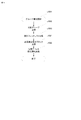
- the new group construction process s1501 is performed when there is no more open page in the open group and the next write destination group becomes necessary. Therefore, it is synonymous with the process of making a group an open group.
- the CPU 206 acquires an unused group number in which no physical block is registered from the virtual address configuration information 1007 (s1502). Subsequently, the CPU 206 acquires an erased empty block list, and acquires the physical block numbers necessary for configuring one group from the list (s1503, s1504). Finally, in s1505, the CPU 206 registers these physical block numbers in the virtual address configuration information 1007, sets the value 0 to the next write position 1202, thereby making the newly created group an open group, and ends the new group construction process. To do.
- the free block list is a list in which physical block numbers of erased physical blocks are registered. It is sufficient that at least one free block list is prepared in the FMPKG 112, but a plurality of free block lists are provided so that an appropriate physical block can be selected according to the use, and the same type of attribute is assigned to each free block list. -You may make it register the physical block number of the empty physical block which has a characteristic.
- an index value indicating the degree of deterioration is calculated and managed based on information on the number of erasures and the like (hereinafter, the index value calculated based on information on the number of erasures is referred to as “degradation degree”.
- a plurality of empty block lists in which empty blocks having a predetermined range of deterioration degree are collected for example, an index value defined by a value (decimal number) from 0 to 1 for the deterioration degree.
- a free block list for managing free physical blocks with a degradation degree of 0 to 0.5 (long life) and a value exceeding the degradation degree 0.5 Select one free block list when executing a new group construction process (for example, providing two free block lists for managing free physical blocks with a short lifetime) A plurality of free physical blocks are selected from the selected single free block list (thereby, all of the selected physical blocks become physical blocks having a degree of deterioration within a predetermined range), and the group is newly constructed. You may make it register.
- the selection method when there are a plurality of free block lists is a method in which the range of the deterioration level is designated in advance by the host device, and the FMPKG 112 selects a free block list that manages the physical blocks in the range of the deterioration degree specified by the host device.
- the FMPKG 112 automatically selects based on information such as an I / O state and an operation time, and any method may be used.
- an empty block list is provided for each physically different unit such as the FM chip 209 and the die (DIE) 401 in order to enable parallel writing when writing data to the FM (that is, In each empty block list, the same FM chip 209 or empty physical blocks in the same die 401 are managed), and when a new group is configured, one empty physical block is acquired in order from each empty block list and grouped. You may make it register. As a result, physical blocks in a plurality of FM chips 209 or a plurality of dies 401 are registered in one group, and parallel writing at the time of data writing to the FM becomes possible.
- RC and RF are processes that have different purposes, but copy valid data in a block to another block and erase the copy source block.
- FMPKG112 which concerns on Example 1 of this invention, RC / RF process is implemented per group. This is because if only one block in the group is erased, it is also necessary to copy a logical page straddling blocks adjacent to the erase target block. However, RC / RF may be performed for each block.
- the CPU 206 first acquires a target group in s1602.
- the RC / RF target is selected by referring to the number of invalid pages 1205 managed in the virtual address configuration information 1007 so that the copy amount is reduced as far as RC is concerned.
- a group is preferentially selected from the group having the largest number of pages 1205.
- the last writing time 1206 is referred to, and a page having a long time elapsed since writing is preferentially selected.
- information regarding reliability may be managed for each group, and a group having a problem with reliability may be selected. In principle, open groups are not selected here.
- a write destination group is selected.
- An open group is selected as the write destination.
- a group suitable for the IO frequency may be selected or newly constructed.
- the CPU 206 determines whether valid data exists in the RC / RF target group (the group selected in s1602). If there is, the CPU 206 copies a part of the valid data onto the buffer 204 in s1605.
- the CPU 206 writes the data copied onto the buffer 204 into the FM by performing the same processing as s1412 (processing from s1405 to s1411) during the write processing described in FIG. However, when the processing of s1412 is performed, in s1406, the group selected in s1603 is acquired as an open group.
- the CPU 206 performs the processes of s1604, s1605, and s1412 until there is no valid data in the RC / RF target group.
- the CPU 206 performs an erasure process on all physical blocks registered in the RC / RF target group.
- the group information is deleted from the virtual address configuration information 1007 (s1610, s1611). The erased block is added to the free block list.
- the FMPKG 112 according to the first embodiment of the present invention is characterized in that the amount of management information does not increase excessively even when the logical page size and the physical page size do not match.
- the amount of management information does not increase excessively even when the logical page size and the physical page size do not match.
- one logical page may be stored across a plurality of physical pages.
- the logical page is associated with a one-dimensional address space called a virtual address space, and a page mapping table is used.
- a page mapping table is used to manage the correspondence between the logical page and the virtual address space. Since the page mapping table stores only one entry representing the position of one logical page, the size of the page mapping table is the logical-physical conversion table in the conventional flash storage (the logical page and the physical page have the same size). Therefore, the size of management information does not increase even when almost all logical pages are stored across two physical pages.
- the FMPKG 112 needs to manage virtual address configuration information for managing the correspondence between the virtual address space and the physical block in addition to the page mapping table.
- the size of the virtual address configuration information is extremely small compared to the logical-physical translation table. This is because the logical-physical conversion table stores information for each page, and the size of the logical-physical conversion table is proportional to the number of pages.
- the virtual address configuration information since the virtual address configuration information stores information for each physical block, the virtual address configuration information has a size proportional to the number of physical blocks.
- the number of physical blocks in the FMPKG 112 is 1/128 of the number of physical pages or There is only 1/256.
- the size of the virtual address configuration information is an extremely small size of 1/100 or less of the logical-physical conversion table. Therefore, having virtual address configuration information does not increase management information so much.
- Example 2 will be described. In the following description, differences from the first embodiment will be mainly described. Therefore, the description of the same configuration and processing as in the first embodiment may be omitted or simplified.
- the FMPKG according to the second embodiment is different from the FMPKG 112 according to the first embodiment in that the FMPKG according to the second embodiment has a function of compressing and / or encrypting write data from the host device. This function may be implemented by the CPU 206 or the ASIC 203 in FIG. 2, or may be provided with dedicated hardware for compression or encryption.
- write data is converted (for example, compressed and encrypted) and stored. However, when the stored data is read, the data is inversely converted (expanded compressed data or encrypted). Therefore, the storage system and the host computer can see the same device as the FMPKG 112 according to the first embodiment. Therefore, the configuration of the storage system according to the second embodiment is the same as that in the first embodiment.
- the logical page straddles the physical page, but this embodiment particularly relates to a processing method when the data size when the logical page is stored varies. State. This is because data conversion such as data compression and encryption is added. In this case, the storage status of each logical page in the flash becomes more complicated.
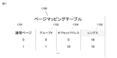
- FIG. 17 shows the contents of the page mapping table 1700 in the second embodiment.
- the FMPKG provides a one-dimensional logical storage space (equivalent to 600 in FIG. 6) to the host device, and this one-dimensional logical space is given a predetermined size (for example, 16 sectors), and each divided area is managed as a logical page.
- the difference from the first embodiment is that data conversion such as compression / encryption is performed, but the data conversion is performed for each logical page. That is, it is not performed to convert (for example, compress) data having a size less than one logical page or to convert (compress) data existing across logical page boundaries.
- the page mapping table 1700 is different from the page mapping table 1002 of the first embodiment in that an item of length 1705 indicating the length of data is added to each entry in the page mapping table 1700. Since the size of each logical page varies due to data conversion, the data size of the logical page after conversion is managed by this entry.
- the unit of the numerical value stored in the item of the length 1705 is, for example, a sector (512 bytes or 520 bytes), but other units (bytes, etc.) may be used. That is, in the page mapping table 1700, information on the range in the virtual address space associated with the data of the logical page after conversion (for example, compression) is managed for each logical page.
- the virtual address configuration information is managed in the same manner as in the first embodiment. However, since the content is the same as the virtual address configuration information 1007 according to the first embodiment, it will not be described here.
- FIG. 18 shows a flow of a conversion process (forward lookup process) from a logical address to a physical address executed by the FMPKG according to the second embodiment. Similar to the forward lookup process in the first embodiment, the logical address is converted into a physical page number when a read request is received from the host device, and the start position of the access target data specified by the read request is a logical page. A process for calculating the physical position of the area for one logical page when the size of the access target data matches the boundary and the size of the access target data is equal to the logical page size will be described.
- FIG. 13 differs from the forward flow (FIG. 13) of the first embodiment in that the processing of s1304 in FIG. 13 (group number and intra-group offset address acquisition processing) is replaced by s1802, and the processing of s1307 in FIG. , S1803.
- the CPU of FMPKG acquires a length 1705 from the page mapping table 1700 in addition to the group number 1703 and the intra-group offset address 1704 of the corresponding logical page. Since the head address in the virtual address space in which the logical page is stored can be acquired from the group number and the offset address, the processing from s1305 to s1306 is performed in the second embodiment as in the first embodiment.
- the CPU calculates the first physical page number and the last physical page number of the access target data.
- the calculation process of the first physical page number is the same as that of the first embodiment, but the length 1705 is used instead of using the size of one logical page in the calculation process of the end physical page number of the access target data.
- the point of calculating the end physical page number using this information is different from that of the first embodiment.
- Other processes are the same as those described in the first embodiment.
- FIG. 19 shows a flow of processing executed when the FMPKG according to the second embodiment receives a write request from the host device. Similar to the description of FIG. 14, here, the description will focus on the case where the write data storage position matches the page boundary of the logical page.
- the difference from the write processing of the first embodiment is that the conversion processing is performed on the data received from the host device stored in the buffer by the processing of s1402 to s1404 (s1902).
- the conversion process may be performed by the CPU of the FMPKG, or the CPU may be implemented by dedicated hardware.
- the CPU checks the amount of data on the buffer with the converted size, and if it is determined that the amount of data on the buffer (the size of the converted data) is greater than or equal to a predetermined size, the CPU 14 is different from the processing of FIG. 14 of the first embodiment in that the length 1705 information is updated when the writing to the management data is started and the management information is updated (s1409).
- the other points are the same as in the first embodiment.
- the process of FIG. 20 differs from the process of FIG. 16 of the first embodiment in that when copying data to the buffer (s1605 of FIG. 16 of the first embodiment), the process of FIG. 20 is a CPU (or dedicated hardware). The point is that data conversion is performed and the converted data is stored in the buffer (s2002). The other points are the same as the RC / RF processing of the first embodiment.
- the management information managed by the FMPKG according to the second embodiment is the page mapping table 1700 and the virtual address configuration information as in the first embodiment.
- the page mapping table 1700 needs to hold data length (length) information as compared with that in the first embodiment, the page mapping table contains one logical page as in the first embodiment. Since the information representing the position of this item needs to be stored only for one entry, the amount of management information does not increase so much.
- Example 3 will be described.
- differences from the first embodiment will be mainly described, and description of the same configuration and processing as those of the first embodiment may be omitted or simplified.
- the size of each physical page is fixed, but in this embodiment, a case where the physical page size is not constant will be described. However, it does not take a completely free size, but there are several patterns of physical pages in one FMPKG. For example, a method of applying an optimum ECC size for each physical page can be considered.
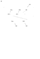
- FIG. 21 shows an example in which a virtual address group (and virtual address space) is configured with devices having blocks having different physical page sizes.
- physical page size characteristics means that all physical page sizes in one physical block are the same, or there are a plurality of types of physical pages having different physical page sizes in the same physical block.
- the physical page size of the physical page between page numbers 0 to n is 7 KB, and the physical pages of page numbers (n + 1) to (n + m) have a physical page size of 8 KB. This means the tendency / distribution of the page size of each physical page in the physical block.
- the type (type) of a physical block having a certain physical page size characteristic is type A
- the type of a physical block having a physical page size characteristic different from type A is type B.
- a virtual address group 2101a in which only a physical block of type A (2102) is registered and a virtual address group 2101b in which only a physical block of type B (2103) is registered are configured. is doing.
- other virtual address groups may be configured.
- a group is composed of blocks of the same type because life management can be facilitated by aligning the characteristics of the blocks in the group, and the physical address associated with the virtual address space of the group from the offset address in the group.
- a block / physical page is specified, there is an advantage in that it can be performed without referring to information of individual blocks.
- FIG. 22 shows virtual address configuration information 2201 in the present embodiment.
- the components of the virtual address configuration information 2201 in the third embodiment are the same as those in the first embodiment from the group 2202 to the last write time 2207. However, the virtual address configuration information 2201 is different from the virtual address configuration information 1007 of the first embodiment in that the information of the block type 2208 associated with the group is held for each group. FMPKG identifies the physical page size of each physical page in the group based on the information stored in the type 2208.
- FIG. 23 shows a flow of a logical address to physical address conversion process (forward lookup process) executed by the FMPKG according to the third embodiment of the present invention.
- the CPU (of FMPKG) acquires the access target logical page number, refers to the page mapping table based on the acquired logical page number, and accesses the logical The group number associated with the page number and the offset address within the group are acquired (s1302 to s1304). Subsequently, the CPU refers to the virtual address configuration information 2201 and acquires the type 2206 (s2302). By this type 2206, the CPU identifies the physical page configuration (size of each physical page) in each physical block constituting the virtual address group, and in subsequent s2303, based on the offset address and physical page configuration in the group, The block number and the offset address in the virtual block are calculated.
- s2304 is processing corresponding to s1306 and s1307 in the first embodiment (FIG. 13).
- the physical address can be calculated simply by dividing the offset address in the virtual block by the physical page size.
- the physical address can be calculated using that information).
- FIG. 24 shows a flow of new group construction processing in the third embodiment.
- the FMPKG according to the third embodiment of the present invention manages the free block list for each type, and the CPU determines the type of the acquisition target block at the time of block acquisition.
- an empty block list of the specified type is acquired (s2402, s2403).
- the flash memory control device 201 constantly monitors the I / O frequency, and if the I / O frequency is high during the new group construction process, it is a relatively reliable physical block type. When a group is constructed from physical blocks corresponding to type A, and the I / O frequency is low, the physical block is not so reliable, and a group is constructed from physical blocks corresponding to type B. Do.
- each block may be managed by a queue or the like divided for each type.
- a method of selecting an optimum type according to the type of stored data may be used.
- the configuration according to the third embodiment is useful when FMPKG using an FM chip having characteristics such as a 3D multilayer chip is used.
- Storage system 102 Storage controller 103: Host computer 104: Management terminal 105: SAN 106: Maintenance interface 107: Host interface 108: CPU 109: Memory 110: Drive interface 112: Flash memory storage device (FMPKG) 201: Flash memory control device 202: Storage interface 203: ASIC 204: Buffer 205: Battery 206: CPU 207: Main memory 208: Flash memory interface 209: Flash memory chip (FM chip) 401: Die 402: Page buffer 403: Physical block 404: Physical page 501: Code Word (CW) 502: Data 503: ECC 1001: Logical page 1002: Page mapping table 1003: Virtual address space 1004: Virtual address group 1006: Virtual block 1007: Virtual address configuration information 1008: Physical block 1009: Physical page
Landscapes
- Engineering & Computer Science (AREA)
- Theoretical Computer Science (AREA)
- Physics & Mathematics (AREA)
- General Engineering & Computer Science (AREA)
- General Physics & Mathematics (AREA)
- Human Computer Interaction (AREA)
- Memory System (AREA)
- Techniques For Improving Reliability Of Storages (AREA)
- Information Retrieval, Db Structures And Fs Structures Therefor (AREA)
Abstract
Priority Applications (3)
| Application Number | Priority Date | Filing Date | Title |
|---|---|---|---|
| JP2015559660A JP6076506B2 (ja) | 2014-01-29 | 2014-01-29 | ストレージ装置 |
| PCT/JP2014/051949 WO2015114754A1 (fr) | 2014-01-29 | 2014-01-29 | Dispositif à mémoire |
| US15/110,581 US10061710B2 (en) | 2014-01-29 | 2014-01-29 | Storage device |
Applications Claiming Priority (1)
| Application Number | Priority Date | Filing Date | Title |
|---|---|---|---|
| PCT/JP2014/051949 WO2015114754A1 (fr) | 2014-01-29 | 2014-01-29 | Dispositif à mémoire |
Publications (1)
| Publication Number | Publication Date |
|---|---|
| WO2015114754A1 true WO2015114754A1 (fr) | 2015-08-06 |
Family
ID=53756373
Family Applications (1)
| Application Number | Title | Priority Date | Filing Date |
|---|---|---|---|
| PCT/JP2014/051949 WO2015114754A1 (fr) | 2014-01-29 | 2014-01-29 | Dispositif à mémoire |
Country Status (3)
| Country | Link |
|---|---|
| US (1) | US10061710B2 (fr) |
| JP (1) | JP6076506B2 (fr) |
| WO (1) | WO2015114754A1 (fr) |
Cited By (6)
| Publication number | Priority date | Publication date | Assignee | Title |
|---|---|---|---|---|
| CN106598504A (zh) * | 2016-12-26 | 2017-04-26 | 华为机器有限公司 | 数据存储方法及装置 |
| WO2017126091A1 (fr) * | 2016-01-21 | 2017-07-27 | 株式会社日立製作所 | Dispositif d'enregistrement, son procédé de contrôle, et système d'enregistrement comprenant le dispositif d'enregistrement |
| CN109032501A (zh) * | 2017-06-12 | 2018-12-18 | 爱思开海力士有限公司 | 存储器系统及其操作方法 |
| CN112100091A (zh) * | 2020-09-17 | 2020-12-18 | 深圳佰维存储科技股份有限公司 | 二级映射表数据映射方法、装置、存储介质及电子设备 |
| CN113590038A (zh) * | 2021-07-27 | 2021-11-02 | 联芸科技(杭州)有限公司 | 固态硬盘的管理方法和固态硬盘 |
| US11409467B2 (en) | 2019-08-28 | 2022-08-09 | Kioxia Corporation | Memory system and method of controlling nonvolatile memory and for reducing a buffer size |
Families Citing this family (13)
| Publication number | Priority date | Publication date | Assignee | Title |
|---|---|---|---|---|
| US10042575B2 (en) * | 2015-03-06 | 2018-08-07 | Toshiba Memory Corporation | Memory system including a battery powered buffer with a storage capacity of that buffer dependent on the voltage level of the battery |
| WO2016194199A1 (fr) * | 2015-06-04 | 2016-12-08 | 株式会社日立製作所 | Dispositif de stockage |
| KR102586628B1 (ko) * | 2015-06-05 | 2023-10-11 | 삼성전자 주식회사 | 전자 장치 및 전자 장치의 메모리 관리 방법 |
| JP6444917B2 (ja) * | 2016-03-08 | 2018-12-26 | 東芝メモリ株式会社 | ストレージシステム、情報処理システムおよび制御方法 |
| US20180060229A1 (en) * | 2016-08-31 | 2018-03-01 | Esab Ab | Techniques for implementing memory segmentation in a welding or cutting system |
| US10423349B2 (en) * | 2017-08-23 | 2019-09-24 | Western Digital Technologies, Inc. | Logical and physical address field size reduction by alignment-constrained writing technique |
| US10606760B2 (en) * | 2017-08-23 | 2020-03-31 | Samsung Electronics Co., Ltd. | Nonvolatile memory devices and methods of controlling the same |
| KR102565895B1 (ko) * | 2017-11-13 | 2023-08-11 | 에스케이하이닉스 주식회사 | 메모리 시스템 및 그것의 동작 방법 |
| US10853168B2 (en) * | 2018-03-28 | 2020-12-01 | Samsung Electronics Co., Ltd. | Apparatus to insert error-correcting coding (ECC) information as data within dynamic random access memory (DRAM) |
| KR102586786B1 (ko) * | 2018-09-28 | 2023-10-11 | 에스케이하이닉스 주식회사 | 메모리 시스템 및 그것의 동작방법 |
| CN112486861B (zh) * | 2020-11-30 | 2024-05-14 | 深圳忆联信息系统有限公司 | 固态硬盘映射表数据查询方法、装置、计算机设备及存储介质 |
| CN113096713B (zh) | 2021-04-12 | 2024-05-07 | 合肥兆芯电子有限公司 | 存储器管理方法、存储器控制电路单元与存储器存储装置 |
| CN114063910B (zh) * | 2021-10-28 | 2024-04-02 | 武汉光迅科技股份有限公司 | 文件处理方法及装置、文件处理系统及存储介质 |
Citations (3)
| Publication number | Priority date | Publication date | Assignee | Title |
|---|---|---|---|---|
| JP2012099139A (ja) * | 2003-12-30 | 2012-05-24 | Sandisk Corp | データラン・プログラミング |
| JP2012113699A (ja) * | 2010-11-26 | 2012-06-14 | Kotatsu Kokusai Denshi Kofun Yugenkoshi | 改良されたフラッシュメモリ互換性の電子デバイスと相関する方法 |
| JP2012173778A (ja) * | 2011-02-17 | 2012-09-10 | Sony Corp | 管理装置、および管理方法 |
Family Cites Families (6)
| Publication number | Priority date | Publication date | Assignee | Title |
|---|---|---|---|---|
| US5623654A (en) * | 1994-08-31 | 1997-04-22 | Texas Instruments Incorporated | Fast fragmentation free memory manager using multiple free block size access table for a free list |
| US7433993B2 (en) | 2003-12-30 | 2008-10-07 | San Disk Corportion | Adaptive metablocks |
| US7529905B2 (en) * | 2005-10-13 | 2009-05-05 | Sandisk Corporation | Method of storing transformed units of data in a memory system having fixed sized storage blocks |
| US8402242B2 (en) * | 2009-07-29 | 2013-03-19 | International Business Machines Corporation | Write-erase endurance lifetime of memory storage devices |
| US9201786B2 (en) * | 2012-12-21 | 2015-12-01 | Kabushiki Kaisha Toshiba | Memory controller and memory system |
| KR20140096875A (ko) * | 2013-01-29 | 2014-08-06 | 삼성전자주식회사 | 메모리 시스템의 및 그것의 블록 관리 방법 |
-
2014
- 2014-01-29 US US15/110,581 patent/US10061710B2/en active Active
- 2014-01-29 WO PCT/JP2014/051949 patent/WO2015114754A1/fr active Application Filing
- 2014-01-29 JP JP2015559660A patent/JP6076506B2/ja active Active
Patent Citations (3)
| Publication number | Priority date | Publication date | Assignee | Title |
|---|---|---|---|---|
| JP2012099139A (ja) * | 2003-12-30 | 2012-05-24 | Sandisk Corp | データラン・プログラミング |
| JP2012113699A (ja) * | 2010-11-26 | 2012-06-14 | Kotatsu Kokusai Denshi Kofun Yugenkoshi | 改良されたフラッシュメモリ互換性の電子デバイスと相関する方法 |
| JP2012173778A (ja) * | 2011-02-17 | 2012-09-10 | Sony Corp | 管理装置、および管理方法 |
Cited By (11)
| Publication number | Priority date | Publication date | Assignee | Title |
|---|---|---|---|---|
| WO2017126091A1 (fr) * | 2016-01-21 | 2017-07-27 | 株式会社日立製作所 | Dispositif d'enregistrement, son procédé de contrôle, et système d'enregistrement comprenant le dispositif d'enregistrement |
| US10802958B2 (en) | 2016-01-21 | 2020-10-13 | Hitachi, Ltd. | Storage device, its controlling method, and storage system having the storage device |
| CN106598504A (zh) * | 2016-12-26 | 2017-04-26 | 华为机器有限公司 | 数据存储方法及装置 |
| CN109032501A (zh) * | 2017-06-12 | 2018-12-18 | 爱思开海力士有限公司 | 存储器系统及其操作方法 |
| CN109032501B (zh) * | 2017-06-12 | 2021-09-17 | 爱思开海力士有限公司 | 存储器系统及其操作方法 |
| US11409467B2 (en) | 2019-08-28 | 2022-08-09 | Kioxia Corporation | Memory system and method of controlling nonvolatile memory and for reducing a buffer size |
| US11662952B2 (en) | 2019-08-28 | 2023-05-30 | Kioxia Corporation | Memory system and method of controlling nonvolatile memory and for reducing a buffer size |
| US12014090B2 (en) | 2019-08-28 | 2024-06-18 | Kioxia Corportion | Memory system and method of controlling nonvolatile memory and for reducing a buffer size |
| CN112100091A (zh) * | 2020-09-17 | 2020-12-18 | 深圳佰维存储科技股份有限公司 | 二级映射表数据映射方法、装置、存储介质及电子设备 |
| CN112100091B (zh) * | 2020-09-17 | 2024-06-11 | 深圳佰维存储科技股份有限公司 | 二级映射表数据映射方法、装置、存储介质及电子设备 |
| CN113590038A (zh) * | 2021-07-27 | 2021-11-02 | 联芸科技(杭州)有限公司 | 固态硬盘的管理方法和固态硬盘 |
Also Published As
| Publication number | Publication date |
|---|---|
| US20160335195A1 (en) | 2016-11-17 |
| JP6076506B2 (ja) | 2017-02-08 |
| JPWO2015114754A1 (ja) | 2017-03-23 |
| US10061710B2 (en) | 2018-08-28 |
Similar Documents
| Publication | Publication Date | Title |
|---|---|---|
| JP6076506B2 (ja) | ストレージ装置 | |
| US11042487B2 (en) | Memory system and method for controlling nonvolatile memory | |
| US10635310B2 (en) | Storage device that compresses data received from a host before writing therein | |
| US9342260B2 (en) | Methods for writing data to non-volatile memory-based mass storage devices | |
| CN105009094B (zh) | 在固态驱动器中利用空闲空间计数来重建两阶加电映射的方法、设备和系统 | |
| US9229876B2 (en) | Method and system for dynamic compression of address tables in a memory | |
| US10606760B2 (en) | Nonvolatile memory devices and methods of controlling the same | |
| US9792067B2 (en) | Trim command processing in a solid state drive | |
| EP2920697B1 (fr) | Procédés, dispositifs de stockage de données et systèmes pour la reconstruction de tableau de micrologiciel fragmenté dans un disque à circuits intégrés | |
| US9304904B2 (en) | Hierarchical flash translation layer | |
| WO2015162758A1 (fr) | Système de stockage | |
| JP7358594B2 (ja) | メモリシステム | |
| JP2016506585A (ja) | データストレージのための方法及びシステム | |
| JP6677740B2 (ja) | ストレージシステム | |
| US20200104047A1 (en) | Container key value store for data storage devices | |
| JP2014519112A (ja) | 記憶デバイスにおいて少ないオーバープロビジョニングで低い書き込み増幅率を実現する方法 | |
| US20190188130A1 (en) | Data Storage Device and Non-Volatile Memory Control Method | |
| WO2015052833A1 (fr) | Dispositif de stockage, système de stockage et procédé de commande de dispositif de stockage | |
| US11093134B2 (en) | Storage device, management method, and program in tiered storage system | |
| US9047959B1 (en) | Data storage device, memory control method, and electronic device with data storage device | |
| TWI726381B (zh) | 資料儲存裝置以及非揮發式記憶體控制方法 | |
| CN117369715A (zh) | 基于存储设备中的引用更新使用回收单元的系统、方法和设备 |
Legal Events
| Date | Code | Title | Description |
|---|---|---|---|
| 121 | Ep: the epo has been informed by wipo that ep was designated in this application |
Ref document number: 14880944 Country of ref document: EP Kind code of ref document: A1 |
|
| ENP | Entry into the national phase |
Ref document number: 2015559660 Country of ref document: JP Kind code of ref document: A |
|
| WWE | Wipo information: entry into national phase |
Ref document number: 15110581 Country of ref document: US |
|
| NENP | Non-entry into the national phase |
Ref country code: DE |
|
| 122 | Ep: pct application non-entry in european phase |
Ref document number: 14880944 Country of ref document: EP Kind code of ref document: A1 |