WO2015087396A1 - 高周波電源用整流回路 - Google Patents
高周波電源用整流回路 Download PDFInfo
- Publication number
- WO2015087396A1 WO2015087396A1 PCT/JP2013/083097 JP2013083097W WO2015087396A1 WO 2015087396 A1 WO2015087396 A1 WO 2015087396A1 JP 2013083097 W JP2013083097 W JP 2013083097W WO 2015087396 A1 WO2015087396 A1 WO 2015087396A1
- Authority
- WO
- WIPO (PCT)
- Prior art keywords
- rectifier circuit
- circuit
- high frequency
- frequency power
- power supply
- Prior art date
- Legal status (The legal status is an assumption and is not a legal conclusion. Google has not performed a legal analysis and makes no representation as to the accuracy of the status listed.)
- Ceased
Links
Images





Classifications
-
- H—ELECTRICITY
- H02—GENERATION; CONVERSION OR DISTRIBUTION OF ELECTRIC POWER
- H02J—ELECTRIC POWER NETWORKS; CIRCUIT ARRANGEMENTS OR SYSTEMS FOR SUPPLYING OR DISTRIBUTING ELECTRIC POWER; SYSTEMS FOR STORING ELECTRIC ENERGY
- H02J50/00—Circuit arrangements or systems for wireless supply or distribution of electric power
- H02J50/20—Circuit arrangements or systems for wireless supply or distribution of electric power using microwaves or radio frequency waves
-
- H—ELECTRICITY
- H02—GENERATION; CONVERSION OR DISTRIBUTION OF ELECTRIC POWER
- H02J—ELECTRIC POWER NETWORKS; CIRCUIT ARRANGEMENTS OR SYSTEMS FOR SUPPLYING OR DISTRIBUTING ELECTRIC POWER; SYSTEMS FOR STORING ELECTRIC ENERGY
- H02J50/00—Circuit arrangements or systems for wireless supply or distribution of electric power
- H02J50/10—Circuit arrangements or systems for wireless supply or distribution of electric power using inductive coupling
- H02J50/12—Circuit arrangements or systems for wireless supply or distribution of electric power using inductive coupling of the resonant type
-
- H—ELECTRICITY
- H02—GENERATION; CONVERSION OR DISTRIBUTION OF ELECTRIC POWER
- H02M—APPARATUS FOR CONVERSION BETWEEN AC AND AC, BETWEEN AC AND DC, OR BETWEEN DC AND DC, AND FOR USE WITH MAINS OR SIMILAR POWER SUPPLY SYSTEMS; CONVERSION OF DC OR AC INPUT POWER INTO SURGE OUTPUT POWER; CONTROL OR REGULATION THEREOF
- H02M7/00—Conversion of AC power input into DC power output; Conversion of DC power input into AC power output
- H02M7/02—Conversion of AC power input into DC power output without possibility of reversal
- H02M7/04—Conversion of AC power input into DC power output without possibility of reversal by static converters
- H02M7/06—Conversion of AC power input into DC power output without possibility of reversal by static converters using discharge tubes without control electrode or semiconductor devices without control electrode
Definitions
- the present invention relates to a rectifier circuit for a high frequency power source that rectifies an AC power source at a high frequency.
- FIG. 13 shows a class E rectifier circuit for rectification in the kHz band according to the prior art.
- this class E rectifier circuit an input 200 kHz AC voltage Vin is rectified, converted into a DC voltage, and output (for example, see Non-Patent Document 1).
- the conventional configuration has a problem that the power conversion efficiency is not good when applied to rectification at a high frequency of the MHz band or higher.
- a circuit with high frequency characteristics is connected to the output impedance, such as a resonant receiving antenna, on the input side, it will affect the operation of its own class E rectifier circuit and maintain its original high-efficiency power conversion operation. I can't.
- the power loss of the circuit that occurs during the rectification operation becomes thermal energy, which leads to a temperature rise of the circuit board. This raises the operating environment temperature of the circuit board and shortens the life of the components used. Therefore, it is necessary to take measures such as providing an exhaust heat device, which causes an increase in cost, an increase in size, and an increase in mass.
- the present invention has been made to solve the above-described problems, and provides a rectifier circuit for a high-frequency power supply capable of obtaining high power conversion efficiency characteristics in rectification of an AC voltage at a high frequency of 2 MHz or higher. It is aimed.
- a rectifier circuit for a high frequency power supply is a rectifier circuit for a high frequency power supply that rectifies an AC voltage at a high frequency of 2 MHz or higher, and a class E rectifier circuit that rectifies an AC voltage input from a power transmission receiving antenna;
- a matching function having a function of adjusting a resonance condition between a resonance circuit that resonates a switching operation at the time of rectification of the class E rectifier circuit and a receiving antenna for power transmission and a function of adjusting a resonance condition between the resonance circuit
- a circuit and a smoothing function circuit that smoothes the voltage rectified by the class E rectifier circuit into a DC voltage.
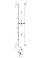
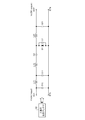
- FIG. 1 is a diagram showing a configuration of a rectifier circuit for a high frequency power supply according to Embodiment 1 of the present invention.
- the rectifier circuit for high-frequency power supply rectifies the AC voltage Vin at a high frequency of 2 MHz or higher.
- the rectifier circuit for a high frequency power source includes a diode D1, capacitors C1 and C2, an inductor L21, a capacitor C21, an inductor L11, and a capacitor C11.
- the resonant receiving antenna (power transmitting receiving antenna) 10 is a power transmitting resonant antenna having LC resonance characteristics (not limited to a non-contact type).
- the resonance receiving antenna 10 may be any of a magnetic field resonance type, an electric field resonance type, and an electromagnetic induction type.
- the diode D1 is a rectifying element that constitutes a class E rectifier circuit for converting the alternating voltage Vin at a high frequency of 2 MHz or higher input from the resonant receiving antenna 10 into a direct current voltage.
- the diode D1 is not limited to a radio frequency (RF) diode, and for example, an element such as a Si-type, SiC-type, or GaN-type diode or a Schottky barrier diode can be used.
- RF radio frequency
- the capacitors C1 and C2 and the inductor L21 constitute a resonance circuit for class E rectification operation in the diode D1 by a composite function. By this resonance circuit, the switching operation at the time of rectification of the diode D1 is resonantly switched.
- the capacitor C1 is a constant configured by a parasitic capacitance of the diode D1 or a composite capacitance with a discrete element.
- a ceramic capacitor or a film capacitor can be used.
- an air core coil, a magnetic body coil, etc. can be used.
- the capacitor C21 is an element constituting a smoothing function circuit for smoothing the ripple voltage rectified by the diode D1 into a DC voltage.
- an element such as a ceramic capacitor, a tantalum capacitor, or a film capacitor can be used.
- the inductor L11 and the capacitor C11 have a function of matching impedance with the resonance receiving antenna 10 on the input side (matching a resonance condition with the resonance receiving antenna 10), and a resonance circuit including the capacitors C1 and C2 and the inductor L21.
- This element constitutes a matching function circuit having a function of matching the impedance of (matching the resonance condition with the resonance circuit).
- the inductor L11 an air-core coil, a magnetic coil, or the like can be used.
- the capacitor C11 a ceramic capacitor, a tantalum capacitor, a film capacitor, or the like can be used.
- the inductor L11 and the capacitor C11 can achieve the resonant switching operation of the diode D1.
- the rectifier circuit for high-frequency power supply has three functions (matching function, class E rectification function, smoothing function) in one circuit configuration, and is not realized by a circuit design in which each is separated. It has become.
- the combined function of the inductor L11 and the capacitor C11 has a function of matching with the output impedance of the resonant receiving antenna 10 and matching with the impedance of the resonant circuit by the capacitors C1 and C2 and the inductor L21.
- the diode D1 has a function of resonantly switching the switching operation at the time of rectification. Thereby, the switching loss of the diode D1 is reduced.
- the switching operation by the diode D1 becomes a resonance switching operation by the combined function of the capacitors C1 and C2 and the inductor L21, and becomes a ZVS (zero voltage switching) state.
- This state is the class E rectification operation, and an operation with little switching loss is achieved.
- the rectified ripple voltage is smoothed to a DC voltage by the capacitor C21 and output.
- impedance matching is performed with a circuit having a high frequency characteristic in the output impedance such as the resonant receiving antenna 10 and the operation is performed as a part of the resonance operation of its own class E rectifier circuit. Therefore, the loss during the rectification operation at a high frequency of the MHz band or higher can be greatly improved, and a high power conversion efficiency (efficiency of 90% or more) can be achieved. In addition, since the power loss of the circuit generated during the rectifying operation is small, the generated heat energy is small and the temperature rise of the circuit board can be suppressed low, so that the influence of the operating environment temperature on the life of the components used can be reduced. Therefore, measures such as providing a conventional heat exhaust device are not required, and cost reduction, size reduction, weight reduction, and low power consumption can be achieved.
- FIG. 1 shows the case where a rectifier circuit for a high frequency power supply is configured using the diode D1, the capacitors C1 and C2, the inductor L21, the capacitor C21, the inductor L11, and the capacitor C11.
- the present invention is not limited to this.
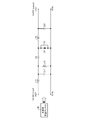
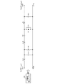
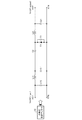
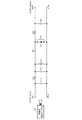
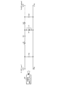
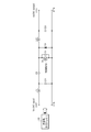
- the rectifier circuit for high-frequency power supply is shown in FIGS. 1 to 9 according to the configuration (output impedance) of the resonant receiving antenna 10 and the input impedance of the device connected to the output (DCoutput) side of the rectifier circuit for high-frequency power supply.
- the optimum configuration is selected.
- the constants of the inductor L11 and the capacitor C11 constituting the matching function circuit are fixed and the resonance condition is fixed.
- the resonance condition variable LC circuit 1 that makes the resonance condition variable may be used.
- FIG. 10 shows the configuration in which the resonance condition variable LC circuit 1 is applied to the configuration of FIG. 8 having the largest number of components among the configurations shown in FIGS. 1 to 9, and the resonance condition variable range becomes the widest.
- the variable resonance condition LC circuit 1 makes the constants of the inductors L11, L12, and L13 and the capacitors C2, C11, and C12 variable.
- the resonance condition variable LC circuit 1 can be applied to FIGS.
- FIG. FIG. 11 is a diagram showing the configuration of a rectifier circuit for high frequency power supply according to Embodiment 2 of the present invention.
- the high frequency power supply rectifier circuit according to the second embodiment shown in FIG. 11 is obtained by changing the diode D1 of the high frequency power supply rectifier circuit according to the first embodiment shown in FIG. 1 to a power element Q1.
- Other configurations are the same, and only the different parts are described with the same reference numerals.
- the power element Q1 is a rectifying element that constitutes a class E rectifier circuit for converting an alternating voltage Vin at a high frequency of 2 MHz or more input from the resonant receiving antenna 10 into a direct voltage.
- the power element Q1 is not limited to a field effect transistor (FET) for high frequency, and for example, an element such as Si-MOSFET, SiC-MOSFET, or GaN-FET can be used.
- Capacitor C1 is configured by a parasitic capacitance of power element Q1 or a composite capacitance with a discrete element. As described above, even when the high-frequency power supply rectifier circuit is configured by using the power element Q1 instead of the diode D1, the same effect as that of the first embodiment can be obtained.
- FIG. 11 shows a configuration in which the diode D1 in FIG. 1 is replaced with a power element Q1.
- the present invention is not limited to this.
- the diode D1 in FIGS. 2 to 9 may be replaced with the power element Q1.
- the rectifier circuit for high-frequency power supply is shown in FIGS. 1 to 9 according to the configuration (output impedance) of the resonant receiving antenna 10 and the input impedance of the device connected to the output (DCoutput) side of the rectifier circuit for high-frequency power supply.
- the optimum configuration is selected from the configurations in which the diode D1 is replaced with the power element Q1.
- the constants of the inductor L11 and the capacitor C11 constituting the matching function circuit are fixed and the resonance condition is fixed.
- the condition variable LC circuit 1 may be used.
- the variable resonance condition LC circuit 1 can be applied to the configuration in which the diode D1 in FIGS. 2 to 9 is replaced with the power element Q1.
- the diode D1 is used as the rectifying element
- the power element Q1 is used as the rectifying element.
- both the diode D1 and the power element Q1 may be used as the rectifying element. 12 is obtained by replacing the rectifying element shown in FIG. 1 with a rectifying element using the diode D1 and the power element Q1, but the present invention is not limited to this.
- the rectifying element shown in FIGS. A rectifying element using D1 and the power element Q1 may be replaced.
- the resonance condition variable LC circuit 1 may be applied to these configurations.
- the invention of the present application can be freely combined with each embodiment, modified with any component in each embodiment, or omitted with any component in each embodiment. .
- the rectifier circuit for a high frequency power source can obtain high power conversion efficiency characteristics in rectifying an AC voltage at a high frequency of 2 MHz or higher, and is used for a rectifier circuit for a high frequency power source that rectifies an AC power source at a high frequency. Suitable for
- Resonance condition variable LC circuit 1 Resonance condition variable LC circuit, 10 Resonant receiving antenna (power transmission receiving antenna).
Landscapes
- Engineering & Computer Science (AREA)
- Power Engineering (AREA)
- Computer Networks & Wireless Communication (AREA)
- Rectifiers (AREA)
- Dc-Dc Converters (AREA)
Abstract
Description
そして、整流動作時に発生する回路の電力損失は、熱エネルギーとなって回路基板の温度上昇に繋がる。これは、回路基板の動作環境温度を上げることになり、使用部品の寿命を短くすることになる。そのため、排熱装置を備えるなどの対策が必要となり、コスト増、大型化、質量増の原因にもなっている。
実施の形態1.
図1はこの発明の実施の形態1に係る高周波電源用整流回路の構成を示す図である。
高周波電源用整流回路は、2MHz以上の高周波における交流電圧Vinの整流を行うものである。この高周波電源用整流回路は、図1に示すように、ダイオードD1、コンデンサC1,C2、インダクタL21、コンデンサC21、インダクタL11及びコンデンサC11から構成されている。
なお、共振型受信アンテナ(電力伝送用受信アンテナ)10は、LC共振特性を持つ電力伝送用の共振型アンテナである(非接触型のみに限定されない)。この共振型受信アンテナ10は、磁界共鳴型、電界共鳴型、電磁誘導型のいずれであってもよい。
まず、共振型受信アンテナ10から2MHz以上の高周波の交流電圧Vinが入力されると、インダクタL11とコンデンサC11による複合機能により、共振型受信アンテナ10の出力インピーダンスとの整合と、コンデンサC1,C2とインダクタL21による共振回路とのインピーダンス整合が図られる。そして、その整合状態を維持しながら、コンデンサC2とダイオードD1により、入力された交流電圧Vinが片側電位(正電位)のリップル電圧に整流される。このとき、ダイオードD1によるスイッチング動作は、コンデンサC1,C2とインダクタL21による複合機能により共振スイッチング動作となり、ZVS(ゼロボルテージスイッチング)状態となる。この状態がE級整流動作であり、スイッチング損失の少ない動作が図られる。そして、整流されたリップル電圧は、コンデンサC21により直流電圧へ平滑され出力される。
以上の一連の動作により、入力された高周波の交流電圧Vinを高い電力変換効率(90%以上)で直流電圧へ整流し出力することが可能である。
また、整流動作時に発生する回路の電力損失が少ないため、発生する熱エネルギーも少なく回路基板の温度上昇を低く抑えられることから、動作環境温度が使用部品の寿命に与える影響を少なくできる。そのため、従来の排熱装置を備えるなどの対策が不要となり、コストの削減、小型、軽量化及び低消費電力化を図ることができる。
図1~7,9についても同様に共振条件可変型LC回路1を適用可能である。
図11はこの発明の実施の形態2に係る高周波電源用整流回路の構成を示す図である。図11に示す実施の形態2に係る高周波電源用整流回路は、図1に示す実施の形態1に係る高周波電源用整流回路のダイオードD1をパワー素子Q1に変更したものである。その他の構成は同様であり、同一の符号を付して異なる部分についてのみ説明を行う。
このように、ダイオードD1に代えてパワー素子Q1を用いて高周波電源用整流回路を構成するようにしても、実施の形態1と同様の効果を得ることができる。
Claims (9)
- 2MHz以上の高周波における交流電圧の整流を行う高周波電源用整流回路であって、
電力伝送用受信アンテナから入力された前記交流電圧を整流するE級整流回路と、
前記E級整流回路の整流の際のスイッチング動作を共振スイッチングさせる共振回路と、
前記電力伝送用受信アンテナとの間で共振条件を合わせる機能及び前記共振回路との間で共振条件を合わせる機能を有する整合機能回路と、
前記E級整流回路により整流された電圧を直流電圧に平滑する平滑機能回路とを備えた
ことを特徴とする高周波電源用整流回路。 - 前記E級整流回路は、ダイオードを用いて構成された
ことを特徴とする請求項1記載の高周波電源用整流回路。 - 前記ダイオードは、高周波用のダイオード以外のダイオードである
ことを特徴とする請求項2記載の高周波電源用整流回路。 - 前記E級整流回路は、電界効果トランジスタを用いて構成された
ことを特徴とする請求項1記載の高周波電源用整流回路。 - 前記E級整流回路は、ダイオード及び電界効果トランジスタを用いて構成された
ことを特徴とする請求項1記載の高周波電源用整流回路。 - 前記整合機能回路は、磁界共鳴による前記電力伝送用受信アンテナとの間で共振条件を合わせる
ことを特徴とする請求項1記載の高周波電源用整流回路。 - 前記整合機能回路は、電界共鳴による前記電力伝送用受信アンテナとの間で共振条件を合わせる
ことを特徴とする請求項1記載の高周波電源用整流回路。 - 前記整合機能回路は、電磁誘導による前記電力伝送用受信アンテナとの間で共振条件を合わせる
ことを特徴とする請求項1記載の高周波電源用整流回路。 - 前記整合機能回路は共振条件を可変とする
ことを特徴とする請求項1記載の高周波電源用整流回路。
Priority Applications (3)
| Application Number | Priority Date | Filing Date | Title |
|---|---|---|---|
| PCT/JP2013/083097 WO2015087396A1 (ja) | 2013-12-10 | 2013-12-10 | 高周波電源用整流回路 |
| JP2015552229A JP6188820B2 (ja) | 2013-12-10 | 2013-12-10 | 高周波電源用整流回路 |
| US15/102,111 US20160308398A1 (en) | 2013-12-10 | 2013-12-10 | Rectifying circuit for high-frequency power supply |
Applications Claiming Priority (1)
| Application Number | Priority Date | Filing Date | Title |
|---|---|---|---|
| PCT/JP2013/083097 WO2015087396A1 (ja) | 2013-12-10 | 2013-12-10 | 高周波電源用整流回路 |
Publications (1)
| Publication Number | Publication Date |
|---|---|
| WO2015087396A1 true WO2015087396A1 (ja) | 2015-06-18 |
Family
ID=53370742
Family Applications (1)
| Application Number | Title | Priority Date | Filing Date |
|---|---|---|---|
| PCT/JP2013/083097 Ceased WO2015087396A1 (ja) | 2013-12-10 | 2013-12-10 | 高周波電源用整流回路 |
Country Status (3)
| Country | Link |
|---|---|
| US (1) | US20160308398A1 (ja) |
| JP (1) | JP6188820B2 (ja) |
| WO (1) | WO2015087396A1 (ja) |
Cited By (2)
| Publication number | Priority date | Publication date | Assignee | Title |
|---|---|---|---|---|
| WO2020194007A1 (ja) | 2019-03-22 | 2020-10-01 | 日産自動車株式会社 | 電力変換装置の制御方法及び電力変換装置 |
| JPWO2023223063A1 (ja) * | 2022-05-17 | 2023-11-23 |
Families Citing this family (3)
| Publication number | Priority date | Publication date | Assignee | Title |
|---|---|---|---|---|
| US20160241159A1 (en) * | 2013-10-31 | 2016-08-18 | Mitsubishi Electric Engineering Company, Limited | Resonant type high frequency power supply device |
| US20200091754A1 (en) * | 2018-09-17 | 2020-03-19 | Newvastek Co., Ltd. | Low-energy-consumption high-frequency wireless charging system for lithium battery |
| CN113381622B (zh) * | 2021-05-21 | 2023-11-03 | 西安理工大学 | 一种用于无线输电高频e类整流器并联电路及控制方法 |
Citations (4)
| Publication number | Priority date | Publication date | Assignee | Title |
|---|---|---|---|---|
| JP2010130800A (ja) * | 2008-11-28 | 2010-06-10 | Nagano Japan Radio Co | 非接触型電力伝送システム |
| JP2012023949A (ja) * | 2010-06-17 | 2012-02-02 | Semiconductor Energy Lab Co Ltd | 送電装置、受電装置、及びそれらを用いた電力供給方法 |
| JP2012135127A (ja) * | 2010-12-22 | 2012-07-12 | Panasonic Corp | 無線電力伝送システム、それに用いられる送電機器および受電機器、ならびに無線電力伝送方法 |
| JP2012521737A (ja) * | 2009-03-20 | 2012-09-13 | クアルコム,インコーポレイテッド | ワイヤレス電力伝送における適応インピーダンス同調 |
Family Cites Families (5)
| Publication number | Priority date | Publication date | Assignee | Title |
|---|---|---|---|---|
| JP2009290950A (ja) * | 2008-05-28 | 2009-12-10 | Kaga Electronics Co Ltd | 電源システム |
| US8278784B2 (en) * | 2008-07-28 | 2012-10-02 | Qualcomm Incorporated | Wireless power transmission for electronic devices |
| US9787364B2 (en) * | 2011-01-20 | 2017-10-10 | Triune Ip, Llc | Multi-use wireless power and data system |
| KR101184503B1 (ko) * | 2010-08-13 | 2012-09-20 | 삼성전기주식회사 | 무선 전력 전송 장치 및 그 전송 방법 |
| JP6088234B2 (ja) * | 2011-12-23 | 2017-03-01 | 株式会社半導体エネルギー研究所 | 受電装置、無線給電システム |
-
2013
- 2013-12-10 JP JP2015552229A patent/JP6188820B2/ja active Active
- 2013-12-10 WO PCT/JP2013/083097 patent/WO2015087396A1/ja not_active Ceased
- 2013-12-10 US US15/102,111 patent/US20160308398A1/en not_active Abandoned
Patent Citations (4)
| Publication number | Priority date | Publication date | Assignee | Title |
|---|---|---|---|---|
| JP2010130800A (ja) * | 2008-11-28 | 2010-06-10 | Nagano Japan Radio Co | 非接触型電力伝送システム |
| JP2012521737A (ja) * | 2009-03-20 | 2012-09-13 | クアルコム,インコーポレイテッド | ワイヤレス電力伝送における適応インピーダンス同調 |
| JP2012023949A (ja) * | 2010-06-17 | 2012-02-02 | Semiconductor Energy Lab Co Ltd | 送電装置、受電装置、及びそれらを用いた電力供給方法 |
| JP2012135127A (ja) * | 2010-12-22 | 2012-07-12 | Panasonic Corp | 無線電力伝送システム、それに用いられる送電機器および受電機器、ならびに無線電力伝送方法 |
Non-Patent Citations (2)
| Title |
|---|
| KAZUHIDE INOUE: "Design of Wireless Power Transfer System through Electromagnetic Induction with Class- DE Transmitter and Class-E Rectifier", PAPERS OF TECHNICAL MEETING ON SEMICONDUCTOR POWER CONVERTER, vol. SPC-13, no. 90 TO, 25 July 2013 (2013-07-25), pages 25 - 30 * |
| ORGHI,D: "Class E Rectifier with MOSFET and no External Driving Circuit", IEICE TECHNICAL REPORT, vol. 100, no. 628, 16 February 2001 (2001-02-16), pages 51 - 56 * |
Cited By (7)
| Publication number | Priority date | Publication date | Assignee | Title |
|---|---|---|---|---|
| WO2020194007A1 (ja) | 2019-03-22 | 2020-10-01 | 日産自動車株式会社 | 電力変換装置の制御方法及び電力変換装置 |
| CN113557657A (zh) * | 2019-03-22 | 2021-10-26 | 日产自动车株式会社 | 功率变换装置的控制方法及功率变换装置 |
| US11616448B2 (en) | 2019-03-22 | 2023-03-28 | Nissan Motor Co., Ltd. | Method for controlling power conversion device and power conversion device |
| CN113557657B (zh) * | 2019-03-22 | 2023-06-13 | 日产自动车株式会社 | 功率变换装置的控制方法及功率变换装置 |
| EP4220922A2 (en) | 2019-03-22 | 2023-08-02 | Nissan Motor Co., Ltd. | Method for controlling power conversion device and power conversion device |
| JPWO2023223063A1 (ja) * | 2022-05-17 | 2023-11-23 | ||
| JP7805449B2 (ja) | 2022-05-17 | 2026-01-23 | 日産自動車株式会社 | 電力変換装置及びその制御方法 |
Also Published As
| Publication number | Publication date |
|---|---|
| JP6188820B2 (ja) | 2017-08-30 |
| US20160308398A1 (en) | 2016-10-20 |
| JPWO2015087396A1 (ja) | 2017-03-16 |
Similar Documents
| Publication | Publication Date | Title |
|---|---|---|
| JP5832317B2 (ja) | 非接触給電回路 | |
| KR102087283B1 (ko) | 고효율 전압 모드 클래스 d 토폴로지 | |
| CN101494421B (zh) | 开关电源装置 | |
| GB2508775A (en) | Switching power-supply device | |
| JP6493526B2 (ja) | ワイヤレス給電システムおよびワイヤレス給電方法 | |
| CN104247206A (zh) | 电力传输系统 | |
| WO2013058174A1 (ja) | スイッチング電源装置 | |
| JP6188820B2 (ja) | 高周波電源用整流回路 | |
| WO2014174785A1 (ja) | 無線電力伝送装置 | |
| JP6188824B2 (ja) | 高周波電源用整流回路 | |
| JP6180548B2 (ja) | 高周波電源用整流回路 | |
| JP5847336B2 (ja) | 高周波電源用整流回路 | |
| JP6188825B2 (ja) | 高周波電源用整流回路 | |
| Truong et al. | Tapped-inductor inverter/rectifier structure with integrated matching network for capacitive power transfer systems | |
| WO2014119059A1 (ja) | 受電装置および送電装置 |
Legal Events
| Date | Code | Title | Description |
|---|---|---|---|
| 121 | Ep: the epo has been informed by wipo that ep was designated in this application |
Ref document number: 13899138 Country of ref document: EP Kind code of ref document: A1 |
|
| ENP | Entry into the national phase |
Ref document number: 2015552229 Country of ref document: JP Kind code of ref document: A |
|
| WWE | Wipo information: entry into national phase |
Ref document number: 15102111 Country of ref document: US |
|
| NENP | Non-entry into the national phase |
Ref country code: DE |
|
| 122 | Ep: pct application non-entry in european phase |
Ref document number: 13899138 Country of ref document: EP Kind code of ref document: A1 |