WO2015040825A2 - Imaging device, manufacturing apparatus, manufacturing method, and electronic apparatus - Google Patents
Imaging device, manufacturing apparatus, manufacturing method, and electronic apparatus Download PDFInfo
- Publication number
- WO2015040825A2 WO2015040825A2 PCT/JP2014/004647 JP2014004647W WO2015040825A2 WO 2015040825 A2 WO2015040825 A2 WO 2015040825A2 JP 2014004647 W JP2014004647 W JP 2014004647W WO 2015040825 A2 WO2015040825 A2 WO 2015040825A2
- Authority
- WO
- WIPO (PCT)
- Prior art keywords
- correction unit
- shape
- liquid
- photoelectric conversion
- imaging plane
- Prior art date
Links
- 238000003384 imaging method Methods 0.000 title claims abstract description 311
- 238000004519 manufacturing process Methods 0.000 title claims description 42
- 238000012937 correction Methods 0.000 claims abstract description 184
- 238000006243 chemical reaction Methods 0.000 claims abstract description 127
- 230000003287 optical effect Effects 0.000 claims abstract description 89
- 239000000463 material Substances 0.000 claims abstract description 51
- 239000007788 liquid Substances 0.000 claims description 168
- 238000000034 method Methods 0.000 claims description 27
- 238000012545 processing Methods 0.000 claims description 14
- 238000003705 background correction Methods 0.000 description 35
- 238000010586 diagram Methods 0.000 description 33
- 230000035945 sensitivity Effects 0.000 description 33
- 230000006870 function Effects 0.000 description 16
- 238000001228 spectrum Methods 0.000 description 16
- 239000007864 aqueous solution Substances 0.000 description 12
- 230000000694 effects Effects 0.000 description 12
- 239000002184 metal Substances 0.000 description 11
- 239000012780 transparent material Substances 0.000 description 11
- 239000003086 colorant Substances 0.000 description 6
- 239000000758 substrate Substances 0.000 description 5
- 239000000853 adhesive Substances 0.000 description 4
- 230000015556 catabolic process Effects 0.000 description 4
- 238000006731 degradation reaction Methods 0.000 description 4
- 239000011347 resin Substances 0.000 description 4
- 229920005989 resin Polymers 0.000 description 4
- 238000010438 heat treatment Methods 0.000 description 3
- 229920001296 polysiloxane Polymers 0.000 description 3
- 230000001131 transforming effect Effects 0.000 description 3
- XLYOFNOQVPJJNP-UHFFFAOYSA-N water Substances O XLYOFNOQVPJJNP-UHFFFAOYSA-N 0.000 description 3
- 206010034960 Photophobia Diseases 0.000 description 2
- 230000008859 change Effects 0.000 description 2
- 238000013461 design Methods 0.000 description 2
- 238000002474 experimental method Methods 0.000 description 2
- 239000011521 glass Substances 0.000 description 2
- 208000013469 light sensitivity Diseases 0.000 description 2
- 239000011159 matrix material Substances 0.000 description 2
- 238000012986 modification Methods 0.000 description 2
- 230000004048 modification Effects 0.000 description 2
- 239000004417 polycarbonate Substances 0.000 description 2
- 229920000515 polycarbonate Polymers 0.000 description 2
- 230000008569 process Effects 0.000 description 2
- 210000001747 pupil Anatomy 0.000 description 2
- 230000004075 alteration Effects 0.000 description 1
- 230000008901 benefit Effects 0.000 description 1
- 238000005401 electroluminescence Methods 0.000 description 1
- 238000005468 ion implantation Methods 0.000 description 1
- 239000004973 liquid crystal related substance Substances 0.000 description 1
- 238000005259 measurement Methods 0.000 description 1
- 230000001151 other effect Effects 0.000 description 1
- 238000005498 polishing Methods 0.000 description 1
- 238000003825 pressing Methods 0.000 description 1
- 230000009467 reduction Effects 0.000 description 1
- 239000007787 solid Substances 0.000 description 1
Images


Classifications
-
- H—ELECTRICITY
- H01—ELECTRIC ELEMENTS
- H01L—SEMICONDUCTOR DEVICES NOT COVERED BY CLASS H10
- H01L27/00—Devices consisting of a plurality of semiconductor or other solid-state components formed in or on a common substrate
- H01L27/14—Devices consisting of a plurality of semiconductor or other solid-state components formed in or on a common substrate including semiconductor components sensitive to infrared radiation, light, electromagnetic radiation of shorter wavelength or corpuscular radiation and specially adapted either for the conversion of the energy of such radiation into electrical energy or for the control of electrical energy by such radiation
- H01L27/144—Devices controlled by radiation
- H01L27/146—Imager structures
- H01L27/14601—Structural or functional details thereof
-
- G—PHYSICS
- G02—OPTICS
- G02B—OPTICAL ELEMENTS, SYSTEMS OR APPARATUS
- G02B27/00—Optical systems or apparatus not provided for by any of the groups G02B1/00 - G02B26/00, G02B30/00
- G02B27/0025—Optical systems or apparatus not provided for by any of the groups G02B1/00 - G02B26/00, G02B30/00 for optical correction, e.g. distorsion, aberration
-
- H—ELECTRICITY
- H04—ELECTRIC COMMUNICATION TECHNIQUE
- H04N—PICTORIAL COMMUNICATION, e.g. TELEVISION
- H04N25/00—Circuitry of solid-state image sensors [SSIS]; Control thereof
- H04N25/60—Noise processing, e.g. detecting, correcting, reducing or removing noise
- H04N25/61—Noise processing, e.g. detecting, correcting, reducing or removing noise the noise originating only from the lens unit, e.g. flare, shading, vignetting or "cos4"
-
- G—PHYSICS
- G02—OPTICS
- G02B—OPTICAL ELEMENTS, SYSTEMS OR APPARATUS
- G02B13/00—Optical objectives specially designed for the purposes specified below
- G02B13/18—Optical objectives specially designed for the purposes specified below with lenses having one or more non-spherical faces, e.g. for reducing geometrical aberration
-
- G—PHYSICS
- G02—OPTICS
- G02B—OPTICAL ELEMENTS, SYSTEMS OR APPARATUS
- G02B26/00—Optical devices or arrangements for the control of light using movable or deformable optical elements
- G02B26/004—Optical devices or arrangements for the control of light using movable or deformable optical elements based on a displacement or a deformation of a fluid
-
- G—PHYSICS
- G02—OPTICS
- G02B—OPTICAL ELEMENTS, SYSTEMS OR APPARATUS
- G02B3/00—Simple or compound lenses
- G02B3/02—Simple or compound lenses with non-spherical faces
- G02B3/04—Simple or compound lenses with non-spherical faces with continuous faces that are rotationally symmetrical but deviate from a true sphere, e.g. so called "aspheric" lenses
-
- G—PHYSICS
- G02—OPTICS
- G02B—OPTICAL ELEMENTS, SYSTEMS OR APPARATUS
- G02B3/00—Simple or compound lenses
- G02B3/12—Fluid-filled or evacuated lenses
-
- G—PHYSICS
- G02—OPTICS
- G02B—OPTICAL ELEMENTS, SYSTEMS OR APPARATUS
- G02B3/00—Simple or compound lenses
- G02B3/12—Fluid-filled or evacuated lenses
- G02B3/14—Fluid-filled or evacuated lenses of variable focal length
-
- H—ELECTRICITY
- H01—ELECTRIC ELEMENTS
- H01L—SEMICONDUCTOR DEVICES NOT COVERED BY CLASS H10
- H01L27/00—Devices consisting of a plurality of semiconductor or other solid-state components formed in or on a common substrate
- H01L27/14—Devices consisting of a plurality of semiconductor or other solid-state components formed in or on a common substrate including semiconductor components sensitive to infrared radiation, light, electromagnetic radiation of shorter wavelength or corpuscular radiation and specially adapted either for the conversion of the energy of such radiation into electrical energy or for the control of electrical energy by such radiation
- H01L27/144—Devices controlled by radiation
- H01L27/146—Imager structures
- H01L27/14601—Structural or functional details thereof
- H01L27/14618—Containers
-
- H—ELECTRICITY
- H01—ELECTRIC ELEMENTS
- H01L—SEMICONDUCTOR DEVICES NOT COVERED BY CLASS H10
- H01L27/00—Devices consisting of a plurality of semiconductor or other solid-state components formed in or on a common substrate
- H01L27/14—Devices consisting of a plurality of semiconductor or other solid-state components formed in or on a common substrate including semiconductor components sensitive to infrared radiation, light, electromagnetic radiation of shorter wavelength or corpuscular radiation and specially adapted either for the conversion of the energy of such radiation into electrical energy or for the control of electrical energy by such radiation
- H01L27/144—Devices controlled by radiation
- H01L27/146—Imager structures
- H01L27/14601—Structural or functional details thereof
- H01L27/14625—Optical elements or arrangements associated with the device
- H01L27/14627—Microlenses
-
- H—ELECTRICITY
- H04—ELECTRIC COMMUNICATION TECHNIQUE
- H04N—PICTORIAL COMMUNICATION, e.g. TELEVISION
- H04N23/00—Cameras or camera modules comprising electronic image sensors; Control thereof
- H04N23/50—Constructional details
- H04N23/55—Optical parts specially adapted for electronic image sensors; Mounting thereof
-
- G—PHYSICS
- G02—OPTICS
- G02B—OPTICAL ELEMENTS, SYSTEMS OR APPARATUS
- G02B3/00—Simple or compound lenses
- G02B2003/0093—Simple or compound lenses characterised by the shape
-
- H—ELECTRICITY
- H01—ELECTRIC ELEMENTS
- H01L—SEMICONDUCTOR DEVICES NOT COVERED BY CLASS H10
- H01L2924/00—Indexing scheme for arrangements or methods for connecting or disconnecting semiconductor or solid-state bodies as covered by H01L24/00
- H01L2924/0001—Technical content checked by a classifier
- H01L2924/0002—Not covered by any one of groups H01L24/00, H01L24/00 and H01L2224/00
-
- H—ELECTRICITY
- H04—ELECTRIC COMMUNICATION TECHNIQUE
- H04N—PICTORIAL COMMUNICATION, e.g. TELEVISION
- H04N2209/00—Details of colour television systems
- H04N2209/04—Picture signal generators
- H04N2209/041—Picture signal generators using solid-state devices
- H04N2209/042—Picture signal generators using solid-state devices having a single pick-up sensor
- H04N2209/047—Picture signal generators using solid-state devices having a single pick-up sensor using multispectral pick-up elements
Definitions
- the present technique relates to imaging devices, manufacturing apparatuses, manufacturing methods, and electronic apparatuses. More particularly, the present technique relates to an imaging device, a manufacturing apparatus, a manufacturing method, and an electronic apparatus that is suitable for correcting shading properties.
- RGB Red, Green, and Blue
- PTLs 1 and 2 disclose pupil correction to be performed on the organic photoelectric conversion films or on-chip lenses of the respective pixels. However, it is not possible to avoid shading due to the difficulty of pupil correction on the red (R) and blue(B) PDs, and color mixing caused by light entering adjacent pixels due to oblique incidence in the PDs.
- PTLs 3 and 4 discloses shading correction to be performed by modifying the lens shapes of on-chip lenses, and converting oblique incidence of light into normal incidence.
- shading correction sufficient to achieve normal incidence of a principal ray can be performed.
- the shapes of the on-chip lenses of the respective pixels are preferably varied in accordance with the inclination of the principal ray.
- PTLs 5 through 7 disclose shading correction by attaching a transparent material having a convex curved surface.
- any specific structure for that has not been disclosed, and there is a possibility that sufficient correction will not be performed, and further degradation will occur, depending on shapes such as curvatures.
- a convex transparent material of a fixed type With a convex transparent material of a fixed type, oblique incidence of a principal ray can be corrected at the nearest end.
- the principal ray enters almost perpendicularly even at the edge of the imaging plane at the furthest end of depth of field. As a result, more characteristics degradation might occur.
- optimum correction is expected to be performed on any incidence angles of principal rays, and optimum shading correction is expected to be performed on any changes in principal rays from the nearest end to the furthest end.
- the present technique has been developed in view of those circumstances, and aims to perform appropriate shading correction.
- An imaging device as disclosed herein includes: a photoelectric conversion unit; and a correction unit configured to correct an angle of light incident on the photoelectric conversion unit, wherein the correction unit is located on a light incident side of the photoelectric conversion unit.
- the correction unit can have a curved surface. More particularly, a surface shape of the curved surface can be a spherical surface, and wherein the surface shape satisfies the following condition: where r represents a radius of the spherical surface, x1 represents a distance from the center of an optical axis of an imaging plane to an edge of the imaging plane, and n represents a refractive index of a material forming the correction unit.
- a surface shape of the curved surface is a spherical surface that satisfies the following condition: where r represents a radius of the spherical surface, x1 represents a distance from the center of an optical axis of an imaging plane to an edge of the imaging plane, and n represents a refractive index of a material forming the correction unit.
- the correction unit has a spherical surface that satisfies the following condition: where r represents a radius of the spherical surface, x1 represents a distance from the center of an optical axis of an imaging plane to an edge of the imaging plane, and n represents a refractive index of a material forming the correction unit.
- the correction unit has a spherical surface that satisfies the following condition: where r represents a radius of the spherical surface, x1 represents a distance from the center of an optical axis of an imaging plane to an edge of the imaging plane, and n represents a refractive index of a material forming the correction unit.
- the correction unit has an aspherical surface that satisfies the following condition: where e represents an angle between a line perpendicular to a surface of the correction unit and a line perpendicular to an imaging plane, n represents a refractive index of a material forming the correction unit, x represents a distance from the center of an optical axis, x1 represents a distance from the center of the optical axis to an edge, a max represents a maximum incidence angle of the light, and a max is from 20 to 30 degrees.
- the correction unit has an aspherical surface that satisfies the following condition: where e represents an angle in degrees between a line perpendicular to a surface of the correction unit and a line perpendicular to an imaging plane, n represents a refractive index of a material forming the correction unit, x represents a distance from the center of an optical axis, x1 represents a distance from the center of the optical axis to an edge, a max represents a maximum incidence angle of the light, and a max is from 20 to 30 degrees.
- the correction unit can be one of a convertible lens and a shape-variable lens, and the surface shape of the correction unit can be controlled by a tension stress.
- the correction unit can be one of a convertible lens and a shape-variable lens formed with two layers of liquids, wherein one of the liquids has a convex interference shape, and wherein the convex interference shape of the one of the liquids is controlled by a voltage application.
- the convex interference shape can be a shape satisfying the following condition: where n is equal to n1/n2, n1 represents a refractive index of a first liquid on a side of the light incidence, n2 represents a refractive index of a second liquid on a side of the photoelectric conversion unit, x1 represents a distance from the center of an optical axis of an imaging plane to an edge of the imaging plane, and r represents a radius of the convex shape, the first liquid and the second liquid being the two layers of liquids.
- the convex interference shape is a shape satisfying the following condition: where n is equal to n1/n2, n1 represents a refractive index of a first liquid on a side of the light incidence, n2 represents a refractive index of a second liquid on a side of the photoelectric conversion unit, x1 represents a distance from the center of an optical axis of an imaging plane to an edge of the imaging plane, and r represents a radius of the convex shape, the first liquid and the second liquid being the two layers of liquids.
- the convex interference shape is a shape satisfying the following condition: where n is equal to n1/n2, n1 represents a refractive index of a first liquid on a side of the light incidence, n2 represents a refractive index of a second liquid on a side of the photoelectric conversion unit, x1 represents a distance from the center of an optical axis of an imaging plane to an edge of the imaging plane, and r represents a radius of the convex shape, the first liquid and the second liquid being the two layers of the liquids.
- the convex interference shape is a shape satisfying the following condition: where n is equal to n1/n2, n1 represents a refractive index of a first liquid on a side of the light incidence, n2 represents a refractive index of a second liquid on a side of the photoelectric conversion unit, x1 represents a distance from the center of an optical axis of an imaging plane to an edge of the imaging plane, and r represents a radius of the convex shape, the first liquid and the second liquid being the two layers of the liquids.
- the convex interference shape is a shape satisfying the following condition: where e represents an angle between a line perpendicular to a surface of the correction unit and a line perpendicular to an imaging plane, n is equal to n1/n2, n1 represents a refractive index of a first liquid on a side of the light incidence, n2 represents a refractive index of a second liquid on a side of the photoelectric conversion unit, x represents a distance from the center of an optical axis, x1 represents a distance from the center of the optical axis to an edge, cmax' represents a maximum incidence angle of the light incident on the second liquid, and dmax' represents a maximum incidence angle of the light in the second liquid, the first liquid and the second liquid being the two layers of the liquids.
- the interference convex shape is a shape satisfying the following condition: where e represents an angle between a line perpendicular to a surface of the correction unit and a line perpendicular to an imaging plane, n is equal to n1/n2, n1 represents a refractive index of a first liquid on a side of the light incidence, n2 represents a refractive index of a second liquid on a side of the photoelectric conversion unit, x represents a distance from the center of an optical axis, x1 represents a distance from the center of the optical axis to an edge, cmax' represents a maximum incidence angle of the light incident on the second liquid, and dmax' represents a maximum incidence angle of the light in the second liquid, the first liquid and the second liquid being the two layers of the liquids.
- An apparatus for manufacturing an imaging device as described herein includes: a photoelectric conversion unit; and a correction unit configured to correct an angle of light incident on the photoelectric conversion unit, the correction unit being located on a light incident side of the photoelectric conversion unit, wherein the correction unit has a curved surface, wherein a surface shape of the curved surface is spherical, and wherein the surface shape satisfies one of the following conditions: where r represents a radius of the spherical surface, x1 represents a distance from the center of an optical axis of an imaging plane to an edge of the imaging plane, and n represents a refractive index of a material forming the correction unit.
- a further apparatus for manufacturing an imaging device as described herein can include: a photoelectric conversion unit; and a correction unit configured to correct an angle of light incident on the photoelectric conversion unit, the correction unit being located on a light incident side of the photoelectric conversion unit, wherein the correction unit has a curved surface, wherein a surface shape of the curved surface is spherical, and wherein the surface shape satisfies one of the following conditions: where r represents a radius of the spherical surface, x1 represents a distance from the center of an optical axis of an imaging plane to an edge of the imaging plane, and n represents a refractive index of a material forming the correction unit.
- a further apparatus for manufacturing an imaging device as described herein can include: a photoelectric conversion unit; and a correction unit configured to correct an angle of light incident on the photoelectric conversion unit, wherein the correction unit is located on a light incident side of the photoelectric conversion unit, wherein the correction unit has a curved surface, wherein a surface shape of the curved surface is aspherical, and wherein the surface shape satisfies one of the following conditions: where e represents an angle between a line perpendicular to a surface of the correction unit and a line perpendicular to an imaging plane, n represents a refractive index of a material forming the correction unit, x represents a distance from the center of an optical axis, x1 represents a distance from the center of the optical axis to an edge, a max represents a maximum incidence angle of the light, and the a max is from 20 to 30 degrees.
- a method of manufacturing an apparatus for manufacturing an imaging device as described herein can include: a photoelectric conversion unit; and a correction unit configured to correct an angle of light incident on the photoelectric conversion unit, the correction unit being located on a light incident side of the photoelectric conversion unit, the method comprising: manufacturing the correction unit, the correction unit having one of: 1) a spherical surface shape; and 2) an aspherical surface shape, wherein the surface shape satisfies one of the following conditions: where r represents a radius of the spherical surface, x1 represents a distance from the center of an optical axis of an imaging plane to an edge of the imaging plane, n represents a refractive index of a material forming the correction unit, a max represents a maximum incidence angle of the light, a represents the incidence angle of the light, and e represents an angle between a line perpendicular to a surface of the correction unit and a line perpendicular to the imaging plane.
- An electronic apparatus as disclosed herein can include: an imaging device including: a photoelectric conversion unit; a correction unit configured to correct an angle of light incident on the photoelectric conversion unit, the correction unit being located on a light incident side of the photoelectric conversion unit; and a signal processing unit configured to perform signal processing on a pixel signal, the pixel signal being output from the photoelectric conversion unit.
- the correction unit that corrects the angle of light incident on a photoelectric conversion unit is designed to be located on the side of the light incident on the photoelectric conversion unit. Also, the correction unit is designed to have a curved surface, and the surface shape of the curved surface is a shape that satisfies a predetermined condition.
- An electronic apparatus of one aspect of the present technique includes: an imaging device that includes: a photoelectric conversion unit; and a correction unit that corrects the angle of light incident on the photoelectric conversion unit, the correction unit being located on the side of the light incident on the photoelectric conversion unit; and a signal processing unit that performs signal processing on a pixel signal that is output from the photoelectric conversion unit.
- the electronic apparatus of one aspect of the present technique is designed to include: an imaging device that includes: a photoelectric conversion unit; and a correction unit that corrects the angle of light incident on the photoelectric conversion unit and is located on the side of the light incident on the photoelectric conversion unit; and a signal processing unit that performs signal processing on a pixel signal that is output from the photoelectric conversion unit.
- shading correction can be appropriately performed.
- Fig. 1 is a diagram for explaining the structure of an imaging device.
- Fig. 2 is a diagram for explaining the relationship between an incidence angle of light and sensitivity.
- Fig. 3 is a diagram for explaining the structure of a correcting lens.
- Fig. 4 is a diagram for explaining the Snell's law.
- Fig. 5 is a diagram for explaining an incidence angle and a radius.
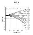
- Fig. 6 is a diagram showing angles of light incident on an imaging device when the incidence angle is 20 degrees.
- Fig. 7 is a diagram showing angles of light incident on an imaging device when the incidence angle is 10 degrees.
- Fig. 8 is a diagram showing angles of light incident on an imaging device when the incidence angle is 30 degrees.
- Fig. 1 is a diagram for explaining the structure of an imaging device.
- Fig. 2 is a diagram for explaining the relationship between an incidence angle of light and sensitivity.
- Fig. 3 is a diagram for explaining the structure of a correcting lens.
- Fig. 4 is
- FIG. 9 is a diagram showing the conditions for the angle of light incident on an imaging device to be 15 degrees or smaller.
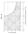
- Fig. 10 is a diagram showing the conditions for the angle of light incident on an imaging device to be 10 degrees or smaller.
- Fig. 11 is a diagram for explaining attachment of a correcting lens onto an imaging device.
- Fig. 12 is a diagram for explaining the manufacture of a correcting lens.
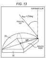
- Fig. 13 is a diagram for explaining the shape of a correcting lens.
- Fig. 14 is a diagram for explaining the effects of a correcting lens.
- Fig. 15 is a diagram showing angles of light incident on an imaging device when the incidence angle is 25 degrees.
- Fig. 16 is a diagram for explaining the shape of a correcting lens.
- FIG. 17 is a diagram for explaining a shape-variable lens.
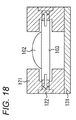
- Fig. 18 is a diagram for explaining a shape-variable lens.
- Fig. 19 is a diagram for explaining a shape-variable lens.
- Fig. 20 is a diagram for explaining a shape-variable lens.
- Fig. 21 is a diagram for explaining a shape-variable lens.
- Fig. 22 is a diagram for explaining an application of a vertical spectrum to an imaging device.
- Fig. 23 is a diagram for explaining an application of a vertical spectrum to an imaging device.
- Fig. 24 is a diagram for explaining the structure of an electronic apparatus.
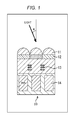
- Fig. 1 schematically shows the structure of an on-chip-lens (OCL) imaging device.
- the imaging device 10 shown in Fig. 1 includes microlenses 11, color filter layers 12, light shielding films 13, and photodiodes (PDs) 14.
- PDs photodiodes
- Light that enters via the microlenses 11 is dispersed in accordance with the colors of the color filter layers 12, and is received by the photodiodes 14.
- the light shielding films 13 are provided between the adjacent photodiodes 14, and are designed to prevent light from leaking into each adjacent photodiode 14.
- a principal ray When a principal ray obliquely enters the imaging device 10 as shown in Fig. 1, sensitivity might become lower, or color mixing might occur due to light leaking into the adjacent photodiodes 14.
- the incidence angle of a principal ray with respect to a line perpendicular to the substrate of the imaging device 10 is defined as "a", as shown in Fig. 1.
- a principal ray is a ray of light that passes through the center of a stop aperture.
- Fig. 2 is a graph showing the shading properties in the imaging device 10. As shown in Fig. 2, the sensitivity becomes lower as the incidence angle "a" becomes larger. Since the incidence angle "a" becomes larger from the chip center toward the chip edge of the imaging device 10, the sensitivity becomes lower from the chip center toward the chip edge.
- the color filter layers 12 are RGB (Red, Green, and Blue) layers. If the respective colors of RGB differ in dependence on the incidence angle "a" from one another, color unevenness might occur. So as to prevent such shading and color unevenness, the length from the microlenses 11 to the photodiodes 14 is shortened, or the aperture ratio is increased. However, a reduction in height or an increase in aperture ratio does not mean that the oblique incidence angle of the principal ray is made smaller, and there is a limit to the correction of shading properties.
- RGB Red, Green, and Blue
- the incidence angle "a" is corrected to be as close to 0 degrees as possible.
- the principal ray enters the substrate perpendicularly, and the highest sensitivity is achieved, as can be seen from Fig. 2.
- the incidence angle "a” is 15 degrees or higher, for example, the sensitivity becomes 0.9 or lower. Therefore, the sensitivity can be maintained at 0.9 or higher by correcting the incidence angle "a" to be 15 degrees or lower.
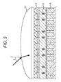
- a correcting lens 31 for shading correcting is provided over the microlenses 11, as shown in Fig. 3.
- the microlenses 11 are arranged in a matrix fashion, and the correcting lens 31 having such a size as to cover all the microlenses 11 are placed at such a position as to cover all the microlenses 11. The conditions to be satisfied by the correcting lens 31 are described below.
- the correcting lens 31 has a curved surface on one side, and a flat surface on the other side.
- the curved surface is a spherical surface or an aspherical surface. A case with a spherical surface and a case with an aspherical surface are described below.
- the correcting lens 31 is formed with a transparent material, and is designed to transmit light.
- a transparent material that can control its shape to form an optimum spherical or aspherical surface satisfying predetermined conditions from the furthest end to the nearest end of depth of field is attached as the correcting lens 31 onto the imaging device 10.
- the incidence angle "a” is preferably adjusted to 15 degrees or less so as to restrict the decrease in sensitivity to 15% or less. More preferably, the incidence angle "a” is adjusted to 10 degrees or less so as to restrict the decrease in sensitivity to 5% or less.
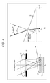
- Fig. 4 is a diagram for explaining the principles of the correcting lens 31 correcting obliquely incident light.
- the correcting lens 31 is attached onto the imaging device 10, and a lens group 51 is provided above the correcting lens 31.
- the principal ray passes through the center of the aperture of a diaphragm 52.
- the principal ray enters perpendicularly with respect to the surface of the imaging device 10, but enters the imaging device 10 more obliquely at portions closer to the edge of the imaging plane.
- Fig. 4B is an enlarged view of the left portion of the correcting lens 31 shown in Fig. 4A.
- the principal ray enters from the left.
- the inclined plane of the correcting lens 31 is higher at the left side, and the Snell's law is observed on this inclined plane.
- the Snell's law is the law for expressing the relationships among the propagation velocities, the incidence angles, and the refraction angles of the travelling waves in two media in a refractive phenomenon of general wave motion, and is also referred to as the law of refraction.
- the refractive index nx is 1, and therefore, the refractive index n is equal to the refractive index ny of the medium y.
- the equation (1) is applied to the situation shown in Fig. 4B.
- This situation is based on the assumption that the angle of incident light is an angle "a" with respect to the direction perpendicular to the imaging plane (the line that is represented by the dashed line in the drawing, and is perpendicular to the imaging plane).
- the angle of the light travelling in the correcting lens 31 with respect to the direction perpendicular to the imaging plane is an angle "d".
- the refractive index of the correcting lens 31 is a refractive index "n”.
- the angle of the direction perpendicular to the inclined plane of the correcting lens 31 (the line that is represented by the thin line in the drawing, and is perpendicular to the inclined plane) with respect to the direction perpendicular to the imaging plane is an angle "b".
- the angle of the direction perpendicular to the inclined plane of the correcting lens 31 (the thin line in the drawing) with respect to the direction perpendicular to the imaging plane inside the correcting lens 31 is an angle "e".
- the equation (2) is converted into the following equation (3).
- the maximum incidence angle "amax” is the angle obtained at the left edge or the right edge of the correcting lens 31.
- ⁇ Shading Correction with a Spherical Shape> A case where the correcting lens 31 has a spherical shape is now described in detail.
- the portion having a curved surface in the correcting lens 31 has the spherical shape.
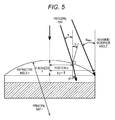
- Fig. 5 is a diagram for explaining the conditions to be satisfied so as to appropriately perform shading correcting when the curved surface of the correcting lens 31 has a spherical shape.
- Fig. 5 is a diagram showing the correcting lens 31, together with the sizes of the respective components and respective distances.
- the same components as those shown in Fig. 4 are denoted by the same reference numerals as those used in Fig. 4.
- the distance from the center of the correcting lens 31 to the position where light enters is represented by a distance x or a position x.
- the distance from the center to the edge of the correcting lens 31 is represented by a distance x0.
- the radius of the spherical portion of the correcting lens 31 is represented by a radius r.
- the principal ray enters at the maximum incidence angle "amax".
- the angle "d" of the principal ray with respect to the line perpendicular to the substrate of the imaging device 10 at the position x inside the correcting lens 31 formed with a transparent material can be calculated by using the above mentioned Snell's law.
- the results of calculations are shown in Figs. 6 through 8.
- the respective graphs shown in Figs. 6 through 8 are graphs formed by plotting the values that are calculated with respective radiuses "r" in cases where the refractive index "n" of the transparent material forming the correcting lens 31 is 1.6, and the radius "r” of the spherical surface is varied.
- the graphs in Fig. 6 are the graphs showing cases where the maximum incidence angle "amax" is 20 degrees
- the graphs in Fig. 7 are the graphs showing cases where the maximum incidence angle "amax” is 10 degrees
- the graphs in Fig. 8 are the graph showing cases where the maximum incidence angle "amax” is 30 degrees.
- the abscissa axis of each of the graphs shown in Figs. 6 through 8 indicates the position "x" relative to the center of the correcting lens 31, and the ordinate axis indicates the angle "d" of travelling light with respect to the perpendicular direction inside the correcting lens 31.
- graph a is the graph showing a case where the radius "r" is 3.4/3
- graph b is the graph showing a case where the radius "r” is 3.6/3
- graph c is the graph showing a case where the radius "r” is 4/3.
- Graph d is the graph showing a case where the radius "r” is 4.3/3
- graph e is the graph showing a case where the radius "r” is 4.7/3
- graph f is the graph showing a case where the radius "r” is 5.5/3
- graph g is the graph showing a case where the radius "r” is 6.2/3
- graph h is the graph showing a case where the radius "r” is 9/3
- graph i is the graph showing a case where the radius "r” is 15/3
- graph j is the graph showing a case where the radius "r” is 29/3
- graph k is the graph showing a case where the radius "r” is 60/3.
- graph a is the graph showing a case where the radius "r” is 4/3
- graph b is the graph showing a case where the radius "r” is 5/3
- graph c is the graph showing a case where the radius "r” is 7/3
- graph d is the graph showing a case where the radius "r” is 10/3
- graph e is the graph showing a case where the radius "r” is 100/3
- graph f is the graph showing a case where the radius "r” is 100000/3.
- graph a is the graph showing a case where the radius "r” is 3.5/3
- graph b is the graph showing a case where the radius "r” is 3.7/3
- graph c is the graph showing a case where the radius "r” is 4.1/3
- graph d is the graph showing a case where the radius "r” is 4.5/3
- graph e is the graph showing a case where the radius "r” is 5/3
- graph f is the graph showing a case where the radius "r” is 7/3
- graph g is the graph showing a case where the radius "r” is 10/3
- graph h is the graph showing a case where the radius "r” is 20/3.
- the correcting lens 31 is effective when the position "x" is 1, or when the angle "d" is smaller than a predetermined angle at the edge of the correcting lens 31. Cases where the predetermined angle is 15 degrees, for example, are now described.
- the graphs showing angles that are outside the range of -15 to 15 degrees when the position x is 1 are graph a and graph b.
- the angle "d" when the maximum incidence angle "amax" is 20 degrees is -20 degrees (20 degrees in absolute value) or smaller. Therefore, the use of the correcting lens 31 is effective, but the angle "d" is not 15 degrees or smaller.
- the sensitivity becomes 0.9 or lower, and the effect of the correcting lens 31 is considered to be small.
- the angle "d" when the maximum incidence angle "amax" is 20 degrees is -20 degrees (20 degrees in absolute value) or larger. Accordingly, with the use of the correcting lens 31, the direction is converted to a more oblique direction. In other words, as can be seen from graph a, it is preferable not to use the correcting lens 31 when the radius "r" of the correcting lens 31 is 3.4/3.
- the angle "d" is 15 degrees or smaller in absolute value, and therefore, the use of the correcting lens 31 is effective for increasing sensitivity. That is, in a case where the correcting lens 31 is designed so that the angle "d" will become 15 degrees or smaller in absolute value, the radius "r" of the correcting lens 31 is preferably in the range of
- graph c and graph k are also excluded. That is, the radius of 4/3 and the radius of 60/3 are also excluded from the radiuses "r" for the correcting lens 31. If the correcting lens 31 is designed so that the angle "d" will become 10 degrees or smaller in absolute value, the radius "r" of the correcting lens 31 is preferably in the range of
- Fig. 7 shows graphs where the maximum incidence angle "amax" is 10 degrees.
- the graph showing an angle that is outside the range of -15 to 15 degrees when the position x is 1 is graph a.
- the angle "d" when the maximum incidence angle "amax" is 10 degrees is -15 degrees (15 degrees in absolute value) or smaller. Accordingly, with the use of the correcting lens 31, the direction is converted to a more oblique direction. In other words, as can be seen from graph a, it is preferable not to use the correcting lens 31 when the radius "r" of the correcting lens 31 is 4/3.
- the angle "d" is 15 degrees or smaller in absolute value, and therefore, sensitivity can be restricted to 0.85 or higher as can be seen from Fig. 2. Accordingly, the use of the correcting lens 31 is effective for increasing or at least maintaining sensitivity. That is, in a case where the correcting lens 31 is designed so that the angle "d" will become 15 degrees or smaller in absolute value, the radius "r" of the correcting lens 31 is preferably in the range of
- the radius "r" of the correcting lens 31 is preferably in the range of
- Fig. 8 shows graphs where the maximum incidence angle "amax" is 30 degrees.
- the graphs showing angles that are outside the range of -15 to 15 degrees when the position x is 1 are graph a and graph b.
- the angle "d" when the maximum incidence angle "amax" is 30 degrees is -30 degrees (30 degrees in absolute value) or smaller, and is smaller than the incidence angle. Accordingly, a certain effect can be expected from the correcting lens 31.
- the angle "d” is -15 degrees (15 degrees in absolute value) or smaller, radiuses "r" that can achieve desired effects are not obtained.
- the angle "d" is 15 degrees or smaller in absolute value, and therefore, sensitivity can be restricted to 0.85 or higher as can be seen from Fig. 2. Accordingly, the use of the correcting lens 31 is effective for increasing sensitivity. That is, in a case where the correcting lens 31 is designed so that the angle "d" will become 15 degrees or smaller in absolute value, the radius "r" of the correcting lens 31 is preferably in the range of
- graph i is also excluded. That is, the radius of 20/3 is also excluded from the radiuses "r" for the correcting lens 31. If the correcting lens 31 is designed so that the angle "d" will become 10 degrees or smaller in absolute value, the radius "r" of the correcting lens 31 is preferably in the range of
- Fig. 9 is a diagram showing the range of the radiuses "r" of the correcting lens 31 for restricting the angle "d” to 15 degrees or smaller in absolute value.
- Fig. 10 is a diagram showing the range of the radiuses "r” of the correcting lens 31 for restricting the angle "d” to 10 degrees or smaller in absolute value.
- the abscissa axis indicates the maximum incidence angle "amax" of the principal ray
- the ordinate axis indicates the radius "r” of the spherical surface of the correcting lens 31.
- the graph in Fig. 9 shows a line m and a line n.
- the radius "r" of the correcting lens 31 satisfies the condition
- the line m satisfies the following equation (4).
- the radius "r" of the correcting lens 31 is equal to or larger than the value calculated according to the equation (4), the angle “d" is almost 15 degrees or smaller in absolute value. So as to restrict the angle “d” to almost 15 degrees or smaller in absolute value, the condition, should be satisfied. Further, the radius "r” is preferably equal to or smaller than the value represented by the line n.
- the angle "d" is almost 15 degrees or smaller in absolute value. So as to restrict the angle "d” to almost 15 degrees or smaller in absolute value, the condition, should be satisfied.
- the travelling direction of light that enters from an oblique direction can be converted by the correcting lens 31, so that the angle "d" (the angle of light incident on the microlenses 11) can be restricted to 15 degrees or smaller in absolute value. Accordingly, the quantity of light that enters the imaging device 10 can be increased, and sensitivity can be made higher.
- the correcting lens 31 has a radius "r" that satisfies the condition, the quantity of light that enters the imaging device 10 can be increased, and sensitivity can be made higher.
- the equations (4) and (5) are equations that are satisfied when the distance x0 from the center to the edge of the correcting lens 31 is "1".
- the distance x0 is 20 mm
- 20 mm is regarded as "1”
- 10 mm is regarded as "0.5”.
- the distance from the center to the edge of the correcting lens 31 may be set as a unit distance, and the other positions may be expressed in ratio.
- the radius "r" of the correcting lens 31 is set according to the equations (4) and (5).
- the equation (6) is formed by multiplying the right-hand side of the equation (4) by x1
- the equation (7) is formed by multiplying the right-hand side of the equation (5) by x1.
- x1 represents the distance from the center portion of the correcting lens 31 (the distance from the optical-axis center to the edge of the imaging plane).
- the radius "r" of the correcting lens 31 may be calculated by using an equation multiplied by x1 in the above manner.
- the graph in Fig. 10 shows a line m' and a line n'. To be distinguished from the line m and the line n shown in Fig. 9, those lines are denoted by alphabets with prime marks. Within the region between the line m' and the line n', the radius "r" of the correcting lens 31 satisfies the condition, The line m' satisfies the following equation (8).
- the radius "r” of the correcting lens 31 is equal to or larger than the value calculated according to the equation (8), the angle “d” is almost 10 degrees or smaller in absolute value. So as to restrict the angle “d” to almost 10 degrees or smaller in absolute value, the radius “r” should be equal to or larger than the value calculated according to the equation (8). Further, the radius "r” is preferably equal to or smaller than the value represented by the line n'.
- the angle "d" is almost 15 degrees or smaller in absolute value. So as to restrict the angle “d” to almost 15 degrees or smaller in absolute value, the condition, should be satisfied.
- the travelling direction of light that enters from an oblique direction can be converted by the correcting lens 31, so that the angle "d" can be restricted to 10 degrees or smaller in absolute value. Accordingly, the quantity of light that enters the imaging device 10 can be increased, and sensitivity can be made higher.
- the correcting lens 31 has a radius "r" that satisfies the condition, the quantity of light that enters the imaging device 10 can be increased, and sensitivity can be made higher.
- the equations (8) and (9) are equations that are satisfied when the distance x0 from the center to the edge of the correcting lens 31 is "1". In a case where the distance x0 from the center to the edge of the correcting lens 31 may not be “1” but may be x1, and x1 is set at any value, the equations (8) and (9) are converted into the following equations (10) and (11), respectively.
- the equation (10) is formed by multiplying the right-hand side of the equation (8) by x1
- the equation (11) is formed by multiplying the right-hand side of the equation (9) by x1.
- x1 represents the distance from the center portion of the correcting lens 31.
- the radius "r" of the correcting lens 31 may be calculated by using an equation multiplied by x1 in the above manner.
- Fig. 11 is a cross-sectional view of the correcting lens 31 attached onto the imaging device 10.
- the correcting lens 31 is placed on the imaging device 10, with a transparent material 41 being interposed in between.
- the photodiodes 14 are provided, and the microlenses 11 are provided at the positions corresponding to the photodiodes 14.
- the photodiodes 14 are arranged in a matrix fashion, and the microlenses 11 are arranged in accordance with the photodiodes 14.
- the correcting lens 31 is designed to have such a size as to cover the photodiodes 14. Where the plane that includes the upper portions of the microlenses 11 and is in contact with the transparent material 41 is the imaging plane 10a, the correcting lens 31 is designed to have such a size as to cover the imaging plane 10a, and is placed at such a position as to cover the imaging plane 10a.
- the radius thereof is a radius "r" within the range described above with reference to Figs. 9 and 10.
- This correcting lens 31 can be manufactured by a manufacturing method as shown in Fig. 12, for example.
- a metal mold 71 is formed.
- An upper portion 71a of the metal mold 71 is the portion for manufacturing the correcting lens 31, and a lower portion 71b of the metal mold 71 is the portion for manufacturing the portion of the transparent material 41 (Fig. 11).
- the curved portion of the upper portion 71a (the inner side of the upper portion 71a) of the metal mold 71 is turned into a smoothly curved surface by metal processing and electrolytic polishing.
- the curve of the curved potion is a curved line that forms part of the circle with the radius "r" of the correcting lens 31 that satisfies the conditions shown in the above equations (4) through (11).
- the inner side of the upper portion 71a is designed to have a shape that satisfies
- step S2 a resin material 72 is inserted in the metal mold 71, and is molded by pressing with heat.
- step S3 the metal mold 71 is removed.
- step S4 the formed correcting lens 31 is bonded onto the imaging device 10 with an adhesive agent.
- the attachment may not be performed with an adhesive agent, but may be performed by heating.
- the resin material 72 optical polycarbonate having a refractive index of 1.60 can be used. Also, a resin material other than polycarbonate or a glass material can be used in place of the resin material 72.
- the refractive index depends on the material forming the correcting lens 31. Therefore, the radius "r" and the thickness "h” in the above equations are calculated with the refractive index of the material that is used as the correcting lens 31, and the metal mold 71 is formed in accordance with those values.
- the maximum incidence angle "amax" of the principal ray at the end of the imaging plane is set at 25 degrees
- the incidence angle "amax” of the principal ray becomes largest at the four corners of the imaging plane, and each corner is located at 3 mm from the center of the imaging plane.
- the radius "r" of the spherical surface of the correcting lens 31 is set at 9 mm to satisfy the equation (5).
- the absolute value of the angle "d" of the principal ray incident on the imaging device 10 is 10 degrees or smaller, and shading properties are greatly corrected. In this case, the equation (4) is also satisfied.
- a radius "r" of 9 mm is equivalent to a radius "r" of 3 (a.u.) in Figs. 9 and 10, for example.
- sensitivity is increased from 0.6 to 0.95 as shown in Fig. 2.
- color shading and color mixing are reduced, and image quality is improved.
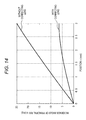
- Fig. 14 shows the results of sensitivity measurement in an imaging device 10 on which the correcting lens 31 satisfying the above described conditions is attached thereon, and in an imaging device 10 not having the correcting lens 31 attached thereon.
- a shading correction effect is shown in Fig. 14, the incidence angle "d" of the principal ray is improved to 6.5 degrees in maximum incidence angle "amax” by attaching the correcting lens 31 having a spherical shape to the imaging device, and has been proved to be 10 degrees or smaller.
- the curved surface of the correcting lens 31 is a spherical surface, and the radius "r" of the spherical surface is made to satisfy predetermined conditions. Accordingly, light that enters from an oblique direction can be converted into light from an almost perpendicular direction, and light sensitivity can be increased.
- the curved surface of the correcting lens 31 has a spherical shape, for example.
- the curved surface of the correcting lens 31 is not limited to a spherical shape. A case where the curved surface of the correcting lens 31 has an aspherical shape is now described in detail.
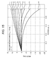
- Fig. 15 is a diagram showing the relationship between the position of the correcting lens 31 and the angle "d" in a case where the correcting lens 31 is designed to have an aspherical shape, as well as graphs showing cases where the correcting lens 31 is designed to have a spherical shape.
- the abscissa axis of each of the graphs shown in Fig. 15 indicates the position "x" relative to the center of the correcting lens 31, and the ordinate axis indicates the angle "d" of travelling light with respect to the perpendicular direction inside the correcting lens 31.
- the graphs in Fig. 15 are graphs showing cases where the maximum incidence angle "amax" is 25 degrees, and the refractive index "n" of the correcting lens 31 is 1.6.
- graphs a through i are graphs showing cases where the correcting lens 31 having a spherical shape is used
- graph j is a graph showing a case where the correcting lens 31 having an aspherical shape is used.
- graph a is the graph showing a case where the radius "r” is 3.5/3
- graph b is the graph showing a case where the radius "r” is 4.2/3
- graph c is the graph showing a case where the radius "r” is 5/3.
- Graph j is the graph showing a case where the correcting lens 31 having an aspherical shape is used, and is also the graph showing a case where the correcting lens 31 having a curved surface that satisfies the following equation (12) is used.
- e represents the angle “e” shown in Fig. 4B.
- the angle “e” is the angle between a line perpendicular to the curved surface of the correcting lens 31 and a line perpendicular to the imaging plane.
- a represents the incidence angle "a”
- n represents the refractive index of the material forming the correcting lens 31.
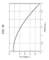
- Fig. 16 is a diagram showing the relationship between the position and the thickness of the correcting lens 31 in a case where the maximum incidence angle "amax" is 25 degrees, the refractive index "n” is 16, and the angle “e” is calculated according to the equation (12) and is converted into the thickness "h” (Fig. 5) of the correcting lens 31.
- the abscissa axis indicates the position x of the correcting lens 31
- the ordinate axis indicates the thickness "h”.
- the curve shown in Fig. 16 indicates the shape of a cross-section of the right half of the correcting lens 31.
- a solid of revolution having the curve shown in Fig. 16 as a curved surface is the correcting lens 31.
- the graph j shown in Fig. 15 is obtained.
- the graphs a through i obtained by using the correcting lens 31 having a spherical shape there are no positions "x" at which the angle "d” is 0 degrees, or there is only one position "x".
- the angle "d" is 0 degrees
- the travelling direction of light that enters from an oblique direction is changed by the correcting lens 31, and light that enters the imaging plane 10a perpendicularly is obtained. Therefore, the larger the number of positions "x" at which the angle "d” is 0 degrees, the better.
- the graph j obtained by using the correcting lens 31 having an aspherical shape indicates 0 degrees at almost all positions. That is, by using the correcting lens 31 having an aspherical shape, light that enters from an oblique direction is converted into light that enters the imaging plane almost perpendicularly at any position "x".
- Such a correcting lens 31 having an aspherical shape can be manufactured in the same manner as in the case where the correcting lens 31 having a spherical shape is manufactured as described above with reference to Fig. 12. Therefore, detailed explanation of the manufacturing method is not repeated herein.
- the metal mold 71 is formed in step S1
- the inner curved surface of the upper portion 71a of the metal mold is calculated according to the equation (12), and the curve shown in Fig. 16 is rotated about the center of the optical axis of the imaging plane, to form a curved surface. In this manner, the correcting lens 31 having an aspherical shape can be manufactured.
- step S4 the manufactured correcting lens 31 is attached onto the imaging device 10.
- the correcting lens 31 having an aspherical shape is designed to have such a size as to cover the photodiodes 14, and is placed at such a position as to cover the photodiodes 14, as described above with reference to Fig. 3.
- the correcting lens 31 having an aspherical shape, light that enters from an oblique direction is converted into light that enters from an almost perpendicular direction. Accordingly, light sensitivity can be increased.
- the metal mold 71 may be formed so that the variation due to the mass production will fall within the range of or more preferably, the range of with respect to the angle "e" calculated according to the equation (12), so as to achieve a sufficient effect.
- sensitivity can be increased by using the correcting lens 31 having a spherical shape or the correcting lens 31 having an aspherical shape.
- a correcting lens is effective in a camera that does not have a telescopic function.
- oblique incidence of a principal ray at the nearest end of depth of field can be corrected, but a principal ray enters almost perpendicularly even at an edge of the imaging plane at the furthest end of depth of field. As a result, degradation in characteristics might occur.
- the correcting lens 31 is a shape-variable lens or a convertible lens, and is attached onto the imaging device 10 so that shading correction can be performed.
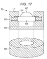
- the lens shown in Fig. 17 can be used, for example.
- This correcting lens 31 can be divided into a lens unit 101 and a transforming unit 121 that changes the shape of the lens.
- the lens unit 101 is formed with a lens 102 and a base 103, and the side surface of the base 103 is connected to a drive unit 122 for the transforming unit 121.
- the lens 102 is formed integrally with the base 103.
- the lens 102 and the base 103 are formed with a silicone lens made of a material that is transparent and elastic, such as silicone.
- a silicone lens made of a material that is transparent and elastic, such as silicone.
- the radius "r” is varied, as the shape of the lens 102 is varied.
- the thickness "h” is varied, as the shape of the lens 102 is varied. The drive unit 122 is operated, and the shape of the lens 102 is changed so that the radius "r” or the thickness "h” has an optimum value at both the nearest end and the furthest end.
- the shape of the surface of the lens 102 is changed to a shape that satisfies the above described conditions and can cope with telescopic situations at the nearest end and the furthest end.
- shading correction from the nearest end to the furthest end can also be performed in a camera that has a telescopic function.
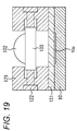
- the lens unit 101 is placed so that the lens unit 101 is located above the imaging plane 10a of the imaging device 10, as shown in Fig. 19.
- a transparent material such as glass 131 is provided, and the correcting lens 31 is placed on the imaging device 10.
- the correcting lens 31 is attached onto the imaging device 10 with an adhesive agent or by heating.
- a liquid lens may be used.
- Fig. 20 shows the structure of a liquid lens 151 serving as the correcting lens 31.
- the upper half of Fig. 20 shows the shape of the liquid lens 151 at a normal time when no voltage is applied, and the lower half shows the shape of the liquid lens 151 at a voltage application time when a voltage is applied.
- the liquid lens 151 is formed with an aqueous solution 152 and oil 153.
- voltage control is performed, the shape of the interface between the two layers of the aqueous solution 152 and the oil 153 can be changed so as to change the shape of the lens.
- the two kinds of liquids which are the aqueous solution 152 and the oil 153, and electrodes 154 are contained therein.
- the aqueous solution 152 moves toward the electrodes 154, and the shape of the plane in contact with the oil 153 changes. In this manner, the interface shape can be changed freely.
- the liquid lens 151 is also provided on the imaging device 10, as shown in Fig. 21A.
- the portion that functions as a lens is placed above the imaging plane 10a of the imaging device 10.
- the intensity of the voltage to be applied to the electrodes 154 varies with telescopic situations.
- the radius "r” is varied, as the interface shape of the liquid lens 151 is varied.
- the thickness "h” is varied, as the interface shape of the liquid lens 151 is varied.
- the voltage to be applied to the electrodes 154 is controlled so that the radius "r” or the thickness "h” has an optimum value at the nearest end and the furthest end.
- the interface shape of the liquid lens 151 is changed to a shape that satisfies the above described conditions and can cope with telescopic situations at the nearest end and the furthest end.
- shading correction from the nearest end to the furthest end can be performed in a camera that has a telescopic function.
- the refractive indexes of the two liquids, the aqueous solution 152 and the oil 153 should be taken into consideration.
- the refractive index of the aqueous solution 152 is a refractive index n1
- the refractive index of the oil 153 is a refractive index n2.
- Fig. 21B The relationship between angles of light that travels from the air into the aqueous solution 152 is shown in Fig. 21B. Specifically, the incidence angle of the principal ray in the air is represented by "a”, and the incidence angle of the principal ray in the aqueous solution 152 is represented by a'.
- the equation (13) shown below is satisfied according to the Snell's law.
- the maximum incidence angle amax' formed when the principal ray enters the aqueous solution 152 from the air is expressed by the equation (14) shown below.
- the incidence angle d' of the principal ray in the oil 153 is the incidence angle of the principal ray incident on the imaging plane 10a. Therefore, in a case where the correcting lens 31 having a spherical shape is used to perform shading correction, "amax" is replaced with amax', "n” is n1/n2, and the equation (16) is satisfied under the condition that or
- the correcting lens 31 can be attached onto the imaging device 10 with an adhesive agent or by heating.
- the liquid lens has a two-layered structure formed with the aqueous solution 152 and the oil 153, and the interface shape is controlled by voltage. Under the shape control, the shape on the side of the oil 153 having the higher refractive index in the two-layered structure is controlled so as to satisfy the above described conditions. In this manner, shading correction is performed.
- the aqueous solution 152 is water
- the radius "r" is 3.9 mm.
- the absolute value of the angle "e” of light incident on the imaging plane is 10 degrees or smaller. Accordingly, sensitivity even to light that enters from an oblique direction can be increased.
- the shape of the surface or the interfacial surface of the lens of the correcting lens 31 is changed, or the change is controlled to satisfy the above described conditions. In this manner, shading correction can be appropriately performed even at the furthest end or the nearest end in a camera having a telescopic function.
- the above described shading correction function can also be applied to an image sensor in which the RGB photodiodes 14 or photoelectric conversion layers are vertically stacked (vertical spectrum), and the effect of the correcting lens 31 is considered to be greater in such an imaging device of a vertical spectrum type.
- Fig. 22 is a diagram for a comparison between a case where shading correction is not performed in the imaging device 10 of the vertical spectrum type, and a case where shading correction is performed in the imaging device 10 of the vertical spectrum type.
- a blue (B) photodiode 14-1, a green (G) photodiode 14-2, and a red (R) photodiode 14-3 are arranged in a vertical direction in this order from the top.
- the imaging device 10 of the vertical spectrum type shown in Fig. 22 is manufactured by forming B-PD, G-PD, and R-PD, which are the photodiodes (PDs) 14 stacked in the vertical direction for dispersing the three primary colors in a Si bulk through ion implantation and epitaxial growth, and then forming transistors and electrodes.
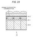
- Fig. 23 schematically shows the imaging device 10 of the vertical spectrum type.
- An organic photoelectric conversion film is provided in an upper portion of the imaging device 10, and transparent electrodes formed with ITO, for example, are formed on and under the organic photoelectric conversion film.
- the organic photoelectric conversion film is interposed between the transparent electrodes.
- a green (G) signal is extracted from the layer of the organic photoelectric conversion film.
- the layer of the organic photoelectric conversion film is equivalent to the green (G) photodiode 14-2 shown in Fig. 22. While the blue photodiode 14-1 is the uppermost photodiode in the imaging device 10 shown in Fig. 22, the green photoelectric conversion region 14-2 is the uppermost photodiode in the structure shown in Fig. 23.
- the arrangement of the photodiodes 14 (photoelectric conversion regions) of the respective colors might vary depending on what kind of method is used as the vertical spectrum. However, the present technique can be used, regardless of the arrangement.
- a Si substrate is provided below the organic photoelectric conversion film, and the photodiode 14-1 for extracting a blue (B) signal and the photodiode 14-3 for extracting a red (R) signal are stacked on the Si substrate.
- the organic photoelectric conversion film for extracting a green signal is located at a distance from the photodiodes 14 for extracting a blue signal and a red signal, and therefore, there is particular concern about color shading.
- color shading properties and color mixing which are particularly problematic in the vertical spectrum, can be prevented as described below.
- the structure of the imaging device 10 of the vertical spectrum type is not limited to the above described structure, and the correcting lens 31 according to the present technique can be used in other structures. Color shading properties and color mixing can be corrected by using the correcting lens 31.
- a principal ray that enters the imaging device 10 from an oblique direction might not reach the red photodiode 14-3 as shown in Fig. 22A, unless the correcting lens 31 is used and shading correction is performed.
- the photodiodes 14-1 through 14-3 differ in sensitivity from one another, and the sensitivity of the photodiode 14-3 becomes particularly lower. In such a situation, there is a possibility that conspicuous color shading will occur.
- Fig. 22B shows a case where one of the above described correcting lenses 31 is used, and shading correction is performed.
- the travelling direction of light that enters from an oblique direction is converted to light that enters the imaging plane almost perpendicularly by the correcting lens 31. Accordingly, the sensitivity variation among the photodiodes 14-1 through 14-3 becomes smaller, and the photodiode 14-3 can be prevented from having a decrease in sensitivity and be designed to absorb sufficient light.
- the correcting lens 31 having an aspherical shape or a spherical shape is used in a camera that does not have a telescopic function, and this correcting lens 31 can be manufactured by the process described above with reference to Fig. 12.
- the above described correcting lens 31 according to the present technique can also be used in the imaging device 10 that is a camera having a telescopic function and is of the vertical spectrum type.
- the correcting lens 31 that has a curved surface of a convex type and is formed with a transparent material is provided on the imaging device 10. Accordingly, shading correction can be performed. Also, according to the present technique, the shape of the curved surface of the correcting lens 31 can be optimized, and the sensitivity of the imaging device 10 can be increased.
- the correcting lens 31 can be optimized by a combination with a shape-variable or convertible lens. Accordingly, optimum shading correction can be continuously performed from the nearest end to the furthest end.
- the present technique can be applied not only to imaging apparatuses, but also to imaging apparatuses such as digital still cameras and video cameras, portable terminal devices each having an imaging function such as portable telephone devices, and general electronic apparatuses that use imaging apparatuses as image capturing units (photoelectric conversion units) such as copying machines that use imaging apparatuses as image reading units.
- imaging apparatuses such as digital still cameras and video cameras
- portable terminal devices each having an imaging function
- general electronic apparatuses that use imaging apparatuses as image capturing units (photoelectric conversion units) such as copying machines that use imaging apparatuses as image reading units.
- image capturing units photoelectric conversion units
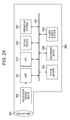
- Fig. 24 is a block diagram showing an example structure of an imaging apparatus that is an example of an electronic apparatus of the present disclosure.
- the imaging apparatus 300 of the present disclosure includes an optical system including a lens group 301 and the like, an imaging device 302, a DSP circuit 303 as a camera signal processing unit, a frame memory 304, a display device 305, a recording device 306, an operating system 307, a power source system 308, and the like.
- the DSP circuit 303, the frame memory 304, the display device 305, the recording device 306, the operating system 307, and the power source system 308 are connected to one another via a bus line 309.
- a CPU 310 controls the respective components in the imaging apparatus 300.
- the lens group 301 captures incident light (image light) from the object, and forms an image on the imaging plane of the imaging device 302.
- the imaging device 302 converts the quantity of the incident light of the image formed on the imaging plane by the lens group 301, into electric signals on a pixel-to-pixel basis, and outputs the electric signals as pixel signals.
- a solid-state imaging device according to the above described embodiment can be used.
- the display device 305 is a panel display device such as a liquid crystal display device or an organic EL (electroluminescence) display device, and displays a moving image or a still image captured by the imaging device 302.
- the recording device 306 records the moving image or the still image captured by the imaging device 302 on a recording medium such as a video tape or a DVD (Digital Versatile Disk).
- the operating system 307 issues operation instructions as to various functions of this imaging apparatus.
- the power source system 308 supplies various kinds of power sources as the operating sources for the DSP circuit 303, the frame memory 304, the display device 305, the recording device 306, and the operating system 307, where necessary.
- Such an imaging apparatus 300 is used in video cameras, digital still cameras, and camera modules for mobile devices such as portable telephone devices.
- an imaging device according to the above described embodiment can be used as the imaging device 302.
- An imaging device including: a photoelectric conversion unit; and a correction unit that corrects the angle of light incident on the photoelectric conversion unit, the correction unit being located on the side of the light incident on the photoelectric conversion unit.
- the correction unit has a curved surface, the surface shape of the curved surface being a spherical surface, the surface shape being a shape that satisfies the following condition: where r represents the radius of the spherical surface, x1 represents the distance from the center of the optical axis of the imaging plane to the edge of the imaging plane, and n represents the refractive index of the material forming the correction unit.
- the correction unit has a curved surface, the surface shape of the curved surface being a spherical surface, the surface shape being a shape that satisfies the following condition: where r represents the radius of the spherical surface, x1 represents the distance from the center of the optical axis of the imaging plane to the edge of the imaging plane, and n represents the refractive index of the material forming the correction unit.
- the correction unit has a curved surface, the surface shape of the curved surface being a spherical surface, the surface shape being a shape that satisfies the following condition: where r represents the radius of the spherical surface, x1 represents the distance from the center of the optical axis of the imaging plane to the edge of the imaging plane, and n represents the refractive index of the material forming the correction unit.
- the correction unit has a curved surface, the surface shape of the curved surface being a spherical surface, the surface shape being a shape that satisfies the following condition: where r represents the radius of the spherical surface, x1 represents the distance from the center of the optical axis of the imaging plane to the edge of the imaging plane, and n represents the refractive index of the material forming the correction unit.
- the correction unit has a curved surface, the surface shape of the curved surface being an aspherical surface, the surface shape being a shape that satisfies the following condition: where e represents the angle between a line perpendicular to the surface of the correction unit and a line perpendicular to the imaging plane, n represents the refractive index of the material forming the correction unit, x represents the distance from the center of the optical axis, x1 represents the distance from the center of the optical axis to the edge, amax represents the maximum incidence angle of the light, and the amax is 20 to 30.
- the correction unit has a curved surface, the surface shape of the curved surface being an aspherical surface, the surface shape being a shape that satisfies the following condition: where e represents the angle between a line perpendicular to the surface of the correction unit and a line perpendicular to the imaging plane, n represents the refractive index of the material forming the correction unit, x represents the distance from the center of the optical axis, x1 represents the distance from the center of the optical axis to the edge, amax represents the maximum incidence angle of the light, and the amax is 20 to 30.
- the correction unit is one of a convertible lens and a shape-variable lens, and is formed with two layers of liquids, the interface shape of one of the liquids being a convex shape, the convex shape being controlled by voltage application.
- the convex shape is a shape that satisfies the following condition: where n1 represents the refractive index of a first liquid on the side of the light incidence, n2 represents the refractive index of a second liquid on the side of the photoelectric conversion unit, n is equal to n1/n2, x1 represents the distance from the center of the optical axis of the imaging plane to the edge of the imaging plane, and r represents the radius of the convex shape, the first liquid and the second liquid being the two layers of the liquids.
- the convex shape is a shape that satisfies the following condition: where n1 represents the refractive index of a first liquid on the side of the light incidence, n2 represents the refractive index of a second liquid on the side of the photoelectric conversion unit, n is equal to n1/n2, x1 represents the distance from the center of the optical axis of the imaging plane to the edge of the imaging plane, and r represents the radius of the convex shape, the first liquid and the second liquid being the two layers of the liquids.
- the convex shape is a shape that satisfies the following condition: where n1 represents the refractive index of a first liquid on the side of the light incidence, n2 represents the refractive index of a second liquid on the side of the photoelectric conversion unit, n is equal to n1/n2, x1 represents the distance from the center of the optical axis of the imaging plane to the edge of the imaging plane, and r represents the radius of the convex shape, the first liquid and the second liquid being the two layers of the liquids.
- the convex shape is a shape that satisfies the following condition: where n1 represents the refractive index of a first liquid on the side of the light incidence, n2 represents the refractive index of a second liquid on the side of the photoelectric conversion unit, n is equal to n1/n2, x1 represents the distance from the center of the optical axis of the imaging plane to the edge of the imaging plane, and r represents the radius of the convex shape, the first liquid and the second liquid being the two layers of the liquids.
- the convex shape is a shape that satisfies the following condition: where e represents the angle between a line perpendicular to the surface of the correction unit and a line perpendicular to the imaging plane, n1 represents the refractive index of a first liquid on the side of the light incidence, n2 represents the refractive index of a second liquid on the side of the photoelectric conversion unit, n is equal to n1/n2, x represents the distance from the center of the optical axis, x1 represents the distance from the center of the optical axis to the edge, cmax' represents the maximum incidence angle of the light incident on the second liquid, and dmax' represents the maximum incidence angle of the light in the second liquid, the first liquid and the second liquid being the two layers of the liquids.
- the convex shape is a shape that satisfies the following condition: where e represents the angle between a line perpendicular to the surface of the correction unit and a line perpendicular to the imaging plane, n1 represents the refractive index of a first liquid on the side of the light incidence, n2 represents the refractive index of a second liquid on the side of the photoelectric conversion unit, n is equal to n1/n2, x represents the distance from the center of the optical axis, x1 represents the distance from the center of the optical axis to the edge, cmax' represents the maximum incidence angle of the light incident on the second liquid, and dmax' represents the maximum incidence angle of the light in the second liquid, the first liquid and the second liquid being the two layers of the liquids.
- An apparatus for manufacturing an imaging device including: a photoelectric conversion unit; and a correction unit that corrects the angle of light incident on the photoelectric conversion unit, the correction unit being located on the side of the light incident on the photoelectric conversion unit, wherein the correction unit is designed to have a curved surface, the surface shape of the curved surface being a spherical surface, the surface shape being a shape that satisfies one of the following conditions: where r represents the radius of the spherical surface, x1 represents the distance from the center of the optical axis of the imaging plane to the edge of the imaging plane, and n represents the refractive index of the material forming the correction unit.
- An apparatus for manufacturing an imaging device including: a photoelectric conversion unit; and a correction unit that corrects the angle of light incident on the photoelectric conversion unit, the correction unit being located on the side of the light incident on the photoelectric conversion unit, wherein the correction unit is designed to have a curved surface, the surface shape of the curved surface being a spherical surface, the surface shape being a shape that satisfies one of the following conditions: where r represents the radius of the spherical surface, x1 represents the distance from the center of the optical axis of the imaging plane to the edge of the imaging plane, and n represents the refractive index of the material forming the correction unit.
- An apparatus for manufacturing an imaging device including: a photoelectric conversion unit; and a correction unit that corrects the angle of light incident on the photoelectric conversion unit, the correction unit being located on the side of the light incident on the photoelectric conversion unit, wherein the correction unit is designed to have a curved surface, the surface shape of the curved surface being an aspherical surface, the surface shape being a shape that satisfies one of the following conditions: where e represents the angle between a line perpendicular to the surface of the correction unit and a line perpendicular to the imaging plane, n represents the refractive index of the material forming the correction unit, x represents the distance from the center of the optical axis, x1 represents the distance from the center of the optical axis to the edge, amax represents the maximum incidence angle of the light, and the amax is 20 to 30.
- a method of manufacturing an apparatus for manufacturing an imaging device including: a photoelectric conversion unit; and a correction unit that corrects the angle of light incident on the photoelectric conversion unit, the correction unit being located on the side of the light incident on the photoelectric conversion unit, the method including: manufacturing the correction unit that is one of a correction unit having a curved surface, the surface shape of the curved surface being a spherical surface, and a correction unit having an aspherical surface, wherein the surface shape is a shape that satisfies one of the following conditions: where r represents the radius of the spherical surface, x1 represents the distance from the center of the optical axis of the imaging plane to the edge of the imaging plane, n represents the refractive index of the material forming the correction unit, amax represents the maximum incidence angle of the light, a represents the incidence angle of the light, and e represents the angle between a line perpendicular to the surface of the correction unit and a line perpendicular to the imaging plane.
- the present disclosure can also take the following forms: (20) An imaging device comprising: a photoelectric conversion unit; and a correction unit configured to correct an angle of light incident on the photoelectric conversion unit, wherein the correction unit is located on a light incident side of the photoelectric conversion unit.
- the correction unit has a curved surface, wherein a surface shape of the curved surface is a spherical surface, and wherein the surface shape satisfies the following condition: where r represents a radius of the spherical surface, x1 represents a distance from the center of an optical axis of an imaging plane to an edge of the imaging plane, and n represents a refractive index of a material forming the correction unit.
- the convex interference shape is a shape satisfying the following condition: where n is equal to n1/n2, n1 represents a refractive index of a first liquid on a side of the light incidence, n2 represents a refractive index of a second liquid on a side of the photoelectric conversion unit, x1 represents a distance from the center of an optical axis of an imaging plane to an edge of the imaging plane, and r represents a radius of the convex shape, the first liquid and the second liquid being the two layers of liquids.
- the convex interference shape is a shape satisfying the following condition: where n is equal to n1/n2, n1 represents a refractive index of a first liquid on a side of the light incidence, n2 represents a refractive index of a second liquid on a side of the photoelectric conversion unit, x1 represents a distance from the center of an optical axis of an imaging plane to an edge of the imaging plane, and r represents a radius of the convex shape, the first liquid and the second liquid being the two layers of liquids.
- the convex interference shape is a shape satisfying the following condition: where n is equal to n1/n2, n1 represents a refractive index of a first liquid on a side of the light incidence, n2 represents a refractive index of a second liquid on a side of the photoelectric conversion unit, x1 represents a distance from the center of an optical axis of an imaging plane to an edge of the imaging plane, and r represents a radius of the convex shape, the first liquid and the second liquid being the two layers of the liquids.
- the convex interference shape is a shape satisfying the following condition: where n is equal to n1/n2, n1 represents a refractive index of a first liquid on a side of the light incidence, n2 represents a refractive index of a second liquid on a side of the photoelectric conversion unit, x1 represents a distance from the center of an optical axis of an imaging plane to an edge of the imaging plane, and r represents a radius of the convex shape, the first liquid and the second liquid being the two layers of the liquids.
- the convex interference shape is a shape satisfying the following condition: where e represents an angle between a line perpendicular to a surface of the correction unit and a line perpendicular to an imaging plane, n is equal to n1/n2, n1 represents a refractive index of a first liquid on a side of the light incidence, n2 represents a refractive index of a second liquid on a side of the photoelectric conversion unit, x represents a distance from the center of an optical axis, x1 represents a distance from the center of the optical axis to an edge, cmax' represents a maximum incidence angle of the light incident on the second liquid, and dmax' represents a maximum incidence angle of the light in the second liquid, the first liquid and the second liquid being the two layers of the liquids.
- the interference convex shape is a shape satisfying the following condition: where e represents an angle between a line perpendicular to a surface of the correction unit and a line perpendicular to an imaging plane, n is equal to n1/n2, n1 represents a refractive index of a first liquid on a side of the light incidence, n2 represents a refractive index of a second liquid on a side of the photoelectric conversion unit, x represents a distance from the center of an optical axis, x1 represents a distance from the center of the optical axis to an edge, cmax' represents a maximum incidence angle of the light incident on the second liquid, and dmax' represents a maximum incidence angle of the light in the second liquid, the first liquid and the second liquid being the two layers of the liquids.
- An apparatus for manufacturing an imaging device including: a photoelectric conversion unit; and a correction unit configured to correct an angle of light incident on the photoelectric conversion unit, the correction unit being located on a light incident side of the photoelectric conversion unit, wherein the correction unit has a curved surface, wherein a surface shape of the curved surface is spherical, and wherein the surface shape satisfies one of the following conditions: where r represents a radius of the spherical surface, x1 represents a distance from the center of an optical axis of an imaging plane to an edge of the imaging plane, and n represents a refractive index of a material forming the correction unit.
- An apparatus for manufacturing an imaging device including: a photoelectric conversion unit; and a correction unit configured to correct an angle of light incident on the photoelectric conversion unit, the correction unit being located on a light incident side of the photoelectric conversion unit, wherein the correction unit has a curved surface, wherein a surface shape of the curved surface is spherical, and wherein the surface shape satisfies one of the following conditions: where r represents a radius of the spherical surface, x1 represents a distance from the center of an optical axis of an imaging plane to an edge of the imaging plane, and n represents a refractive index of a material forming the correction unit.
- An apparatus for manufacturing an imaging device including: a photoelectric conversion unit; and a correction unit configured to correct an angle of light incident on the photoelectric conversion unit, wherein the correction unit is located on a light incident side of the photoelectric conversion unit, wherein the correction unit has a curved surface, wherein a surface shape of the curved surface is aspherical, and wherein the surface shape satisfies one of the following conditions: where e represents an angle between a line perpendicular to a surface of the correction unit and a line perpendicular to an imaging plane, n represents a refractive index of a material forming the correction unit, x represents a distance from the center of an optical axis, x1 represents a distance from the center of the optical axis to an edge, a max represents a maximum incidence angle of the light, and the a max is from 20 to 30 degrees.
- a method of manufacturing an apparatus for manufacturing an imaging device including: a photoelectric conversion unit; and a correction unit configured to correct an angle of light incident on the photoelectric conversion unit, the correction unit being located on a light incident side of the photoelectric conversion unit, the method comprising: manufacturing the correction unit, the correction unit having one of: 1) a spherical surface shape; and 2) an aspherical surface shape, wherein the surface shape satisfies one of the following conditions: where r represents a radius of the spherical surface, x1 represents a distance from the center of an optical axis of an imaging plane to an edge of the imaging plane, n represents a refractive index of a material forming the correction unit, a max represents a maximum incidence angle of the light, a represents the incidence angle of the light, and e represents an angle between a line perpendicular to a surface of the correction unit and a line perpendicular to the imaging plane.
- An electronic apparatus comprising: an imaging device including: a photoelectric conversion unit; and a correction unit configured to correct an angle of light incident on the photoelectric conversion unit, the correction unit being located on a light incident side of the photoelectric conversion unit; and a signal processing unit configured to perform signal processing on a pixel signal, the pixel signal being output from the photoelectric conversion unit.
- An electronic apparatus including: an imaging device including: a photoelectric conversion unit; and a correction unit that corrects the angle of light incident on the photoelectric conversion unit, the correction unit being located on the side of the light incident on the photoelectric conversion unit; and a signal processing unit that performs signal processing on a pixel signal that is output from the photoelectric conversion unit.
- Imaging device 11 Microlens 12 Color filter layer 13 Light shielding layer 14 Photodiode 31 Correcting lens 101 Lens unit 121 Transforming unit 151 Liquid lens 152 Aqueous solution 153 Oil 154 Electrode
Landscapes
- Physics & Mathematics (AREA)
- General Physics & Mathematics (AREA)
- Engineering & Computer Science (AREA)
- Power Engineering (AREA)
- Optics & Photonics (AREA)
- Electromagnetism (AREA)
- Condensed Matter Physics & Semiconductors (AREA)
- Computer Hardware Design (AREA)
- Microelectronics & Electronic Packaging (AREA)
- Signal Processing (AREA)
- Multimedia (AREA)
- Lenses (AREA)
- Solid State Image Pick-Up Elements (AREA)
- Transforming Light Signals Into Electric Signals (AREA)
- Studio Devices (AREA)
Abstract
Description
This application claims the benefit of Japanese Priority Patent Application JP 2013-193376 filed on September 18, 2013, the entire contents of which are incorporated herein by reference.


1. Shading correction
2. Conditions to be satisfied by a correcting lens
3. Shading correction with a spherical shape
4. Attachment of a spherical correcting lens to an imaging device
5. Manufacture of a correcting lens
6. Shading correction with an aspherical shape
7. Shading correction by a correcting lens having a telescopic function
8. Shading correction with vertical spectrum
9. Electronic apparatus
In camera optics, it is known that sensitivity becomes lower at a location further away from the center of the imaging plane due to oblique incidence of a principal ray. Such a decrease in sensitivity is called "shading", for example. Since the present technique described below is suitable for shading correction, examples of shading correction will be explained below.
As shown in Fig. 3, the correcting
A case where the correcting
a = Tan[x/(x1/ArcTan[amax])]


Fig. 11 is a cross-sectional view of the correcting
This correcting
In the above described embodiment, the curved surface of the correcting

As described above, sensitivity can be increased by using the correcting
"amax" is replaced with amax', "n" is n1/n2, and the equation (16) is satisfied under the condition that
The above described shading correction function can also be applied to an image sensor in which the RGB photodiodes 14 or photoelectric conversion layers are vertically stacked (vertical spectrum), and the effect of the correcting
The present technique can be applied not only to imaging apparatuses, but also to imaging apparatuses such as digital still cameras and video cameras, portable terminal devices each having an imaging function such as portable telephone devices, and general electronic apparatuses that use imaging apparatuses as image capturing units (photoelectric conversion units) such as copying machines that use imaging apparatuses as image reading units. There are cases where the form of the above described module mounted on an electronic apparatus, or a camera module, serves as an imaging apparatus.
(1)
An imaging device including:
a photoelectric conversion unit; and
a correction unit that corrects the angle of light incident on the photoelectric conversion unit, the correction unit being located on the side of the light incident on the photoelectric conversion unit.
(2)
The imaging device of (1), wherein the correction unit has a curved surface, the surface shape of the curved surface being a spherical surface, the surface shape being a shape that satisfies the following condition:

(3)
The imaging device of (1), wherein the correction unit has a curved surface, the surface shape of the curved surface being a spherical surface, the surface shape being a shape that satisfies the following condition:

(4)
The imaging device of (1), wherein the correction unit has a curved surface, the surface shape of the curved surface being a spherical surface, the surface shape being a shape that satisfies the following condition:

(5)
The imaging device of (1), wherein the correction unit has a curved surface, the surface shape of the curved surface being a spherical surface, the surface shape being a shape that satisfies the following condition:

(6)
The imaging device of (1), wherein the correction unit has a curved surface, the surface shape of the curved surface being an aspherical surface, the surface shape being a shape that satisfies the following condition:

(7)
The imaging device of (1), wherein the correction unit has a curved surface, the surface shape of the curved surface being an aspherical surface, the surface shape being a shape that satisfies the following condition:

(8)
The imaging device of any of (1) through (7), wherein the correction unit is one of a convertible lens and a shape-variable lens, and has the surface shape controlled by tension stress.
(9)
The imaging device of any of (1) through (7), wherein the correction unit is one of a convertible lens and a shape-variable lens, and is formed with two layers of liquids, the interface shape of one of the liquids being a convex shape, the convex shape being controlled by voltage application.
(10)
The imaging device of (9), wherein the convex shape is a shape that satisfies the following condition:

(11)
The imaging device of (9), wherein the convex shape is a shape that satisfies the following condition:

(12)
The imaging device of (9), wherein the convex shape is a shape that satisfies the following condition:

(13)
The imaging device of (9), wherein the convex shape is a shape that satisfies the following condition:

(14)
The imaging device of (9), wherein the convex shape is a shape that satisfies the following condition:

(15)
The imaging device of (9), wherein the convex shape is a shape that satisfies the following condition:

(16)
An apparatus for manufacturing an imaging device including:
a photoelectric conversion unit; and
a correction unit that corrects the angle of light incident on the photoelectric conversion unit, the correction unit being located on the side of the light incident on the photoelectric conversion unit,
wherein the correction unit is designed to have a curved surface, the surface shape of the curved surface being a spherical surface, the surface shape being a shape that satisfies one of the following conditions:

(17)
An apparatus for manufacturing an imaging device including:
a photoelectric conversion unit; and
a correction unit that corrects the angle of light incident on the photoelectric conversion unit, the correction unit being located on the side of the light incident on the photoelectric conversion unit,
wherein the correction unit is designed to have a curved surface, the surface shape of the curved surface being a spherical surface, the surface shape being a shape that satisfies one of the following conditions:

(18)
An apparatus for manufacturing an imaging device including:
a photoelectric conversion unit; and
a correction unit that corrects the angle of light incident on the photoelectric conversion unit, the correction unit being located on the side of the light incident on the photoelectric conversion unit,
wherein the correction unit is designed to have a curved surface, the surface shape of the curved surface being an aspherical surface, the surface shape being a shape that satisfies one of the following conditions:

(19)
A method of manufacturing an apparatus for manufacturing an imaging device including:
a photoelectric conversion unit; and
a correction unit that corrects the angle of light incident on the photoelectric conversion unit, the correction unit being located on the side of the light incident on the photoelectric conversion unit,
the method including:
manufacturing the correction unit that is one of a correction unit having a curved surface, the surface shape of the curved surface being a spherical surface, and a correction unit having an aspherical surface,
wherein the surface shape is a shape that satisfies one of the following conditions:

The present disclosure can also take the following forms:
(20)
An imaging device comprising:
a photoelectric conversion unit; and
a correction unit configured to correct an angle of light incident on the photoelectric conversion unit, wherein the correction unit is located on a light incident side of the photoelectric conversion unit.
(21)
The imaging device of (20), wherein the correction unit has a curved surface, wherein a surface shape of the curved surface is a spherical surface, and wherein the surface shape satisfies the following condition:

(22)
The imaging device of (20), wherein the correction unit has a curved surface, wherein a surface shape of the curved surface is a spherical surface, and wherein the surface shape satisfies the following condition:

(23)
The imaging device of (20), wherein the correction unit has a curved surface, wherein a surface shape of the curved surface is a spherical surface, and wherein the surface shape satisfies the following condition:

(24)
The imaging device of (20), wherein the correction unit has a curved surface, wherein a surface shape of the curved surface is a spherical surface, and wherein the surface shape satisfies the following condition:

(25)
The imaging device of (20), wherein the correction unit has a curved surface, wherein a surface shape of the curved surface is an aspherical surface, and wherein the surface shape satisfies the following condition:

(26)
The imaging device of (20), wherein the correction unit has a curved surface, wherein a surface shape of the curved surface is an aspherical surface, and wherein the surface shape satisfies the following condition:

(27)
The imaging device of (20), wherein the correction unit is one of a convertible lens and a shape-variable lens, and wherein the surface shape of the correction unit is controlled by a tension stress.
(28)
The imaging device of (20), wherein the correction unit is one of a convertible lens and a shape-variable lens, wherein the correction unit is formed with two layers of liquids, wherein one of the liquids has a convex interference shape, and wherein the convex interference shape of the one of the liquids is controlled by a voltage application.
(29)
The imaging device of (28), wherein the convex interference shape is a shape satisfying the following condition:

(30)
The imaging device according of (28), wherein the convex interference shape is a shape satisfying the following condition:

(31)
The imaging device of (28), wherein the convex interference shape is a shape satisfying the following condition:

(32)
The imaging device of (28), wherein the convex interference shape is a shape satisfying the following condition:

(33)
The imaging device of (28), wherein the convex interference shape is a shape satisfying the following condition:

(34)
The imaging device of (28), wherein the interference convex shape is a shape satisfying the following condition:

(35)
An apparatus for manufacturing an imaging device including:
a photoelectric conversion unit; and
a correction unit configured to correct an angle of light incident on the photoelectric conversion unit, the correction unit being located on a light incident side of the photoelectric conversion unit,
wherein the correction unit has a curved surface, wherein a surface shape of the curved surface is spherical, and wherein the surface shape satisfies one of the following conditions:

(36)
An apparatus for manufacturing an imaging device including:
a photoelectric conversion unit; and
a correction unit configured to correct an angle of light incident on the photoelectric conversion unit, the correction unit being located on a light incident side of the photoelectric conversion unit,
wherein the correction unit has a curved surface, wherein a surface shape of the curved surface is spherical, and wherein the surface shape satisfies one of the following conditions:

(37)
An apparatus for manufacturing an imaging device including:
a photoelectric conversion unit; and
a correction unit configured to correct an angle of light incident on the photoelectric conversion unit, wherein the correction unit is located on a light incident side of the photoelectric conversion unit,
wherein the correction unit has a curved surface, wherein a surface shape of the curved surface is aspherical, and wherein the surface shape satisfies one of the following conditions:

(38)
A method of manufacturing an apparatus for manufacturing an imaging device including:
a photoelectric conversion unit; and
a correction unit configured to correct an angle of light incident on the photoelectric conversion unit, the correction unit being located on a light incident side of the photoelectric conversion unit,
the method comprising:
manufacturing the correction unit, the correction unit having one of: 1) a spherical surface shape; and 2) an aspherical surface shape,
wherein the surface shape satisfies one of the following conditions:

(39)
An electronic apparatus comprising:
an imaging device including:
a photoelectric conversion unit; and
a correction unit configured to correct an angle of light incident on the photoelectric conversion unit, the correction unit being located on a light incident side of the photoelectric conversion unit; and
a signal processing unit configured to perform signal processing on a pixel signal, the pixel signal being output from the photoelectric conversion unit.
(40)
An electronic apparatus including:
an imaging device including:
a photoelectric conversion unit; and
a correction unit that corrects the angle of light incident on the photoelectric conversion unit, the correction unit being located on the side of the light incident on the photoelectric conversion unit; and
a signal processing unit that performs signal processing on a pixel signal that is output from the photoelectric conversion unit.
11 Microlens
12 Color filter layer
13 Light shielding layer
14 Photodiode
31 Correcting lens
101 Lens unit
121 Transforming unit
151 Liquid lens
152 Aqueous solution
153 Oil
154 Electrode
Claims (20)
- An imaging device comprising:
a photoelectric conversion unit; and
a correction unit configured to correct an angle of light incident on the photoelectric conversion unit, wherein the correction unit is located on a light incident side of the photoelectric conversion unit. - The imaging device according to claim 1, wherein the correction unit has a curved surface, wherein a surface shape of the curved surface is a spherical surface, and wherein the surface shape satisfies the following condition:
where r represents a radius of the spherical surface, x1 represents a distance from the center of an optical axis of an imaging plane to an edge of the imaging plane, and n represents a refractive index of a material forming the correction unit.
- The imaging device according to claim 1, wherein the correction unit has a curved surface, wherein a surface shape of the curved surface is a spherical surface, and wherein the surface shape satisfies the following condition:
where r represents a radius of the spherical surface, x1 represents a distance from the center of an optical axis of an imaging plane to an edge of the imaging plane, and n represents a refractive index of a material forming the correction unit.
- The imaging device according to claim 1, wherein the correction unit has a curved surface, wherein a surface shape of the curved surface is an aspherical surface, and wherein the surface shape satisfies the following condition:
where e represents an angle between a line perpendicular to a surface of the correction unit and a line perpendicular to an imaging plane, n represents a refractive index of a material forming the correction unit, x represents a distance from the center of an optical axis, x1 represents a distance from the center of the optical axis to an edge, amax represents a maximum incidence angle of the light, and amax is from 20 to 30 degrees.
- The imaging device according to claim 1, wherein the correction unit has a curved surface, wherein a surface shape of the curved surface is an aspherical surface, and wherein the surface shape satisfies the following condition:
where e represents an angle in degrees between a line perpendicular to a surface of the correction unit and a line perpendicular to an imaging plane, n represents a refractive index of a material forming the correction unit, x represents a distance from the center of an optical axis, x1 represents a distance from the center of the optical axis to an edge, amax represents a maximum incidence angle of the light, and amax is from 20 to 30 degrees.
- The imaging device according to claim 1, wherein the correction unit is one of a convertible lens and a shape-variable lens, and wherein the surface shape of the correction unit is controlled by a tension stress.
- The imaging device according to claim 1, wherein the correction unit is one of a convertible lens and a shape-variable lens, wherein the correction unit is formed with two layers of liquids, wherein one of the liquids has a convex interference shape, and wherein the convex interference shape of the one of the liquids is controlled by a voltage application.
- The imaging device according to claim 9, wherein the convex interference shape is a shape satisfying the following condition:
where n is equal to n1/n2, n1 represents a refractive index of a first liquid on a side of the light incidence, n2 represents a refractive index of a second liquid on a side of the photoelectric conversion unit, x1 represents a distance from the center of an optical axis of an imaging plane to an edge of the imaging plane, and r represents a radius of the convex shape, the first liquid and the second liquid being the two layers of liquids.
- The imaging device according to claim 9, wherein the convex interference shape is a shape satisfying the following condition:
where n is equal to n1/n2, n1 represents a refractive index of a first liquid on a side of the light incidence, n2 represents a refractive index of a second liquid on a side of the photoelectric conversion unit, x1 represents a distance from the center of an optical axis of an imaging plane to an edge of the imaging plane, and r represents a radius of the convex shape, the first liquid and the second liquid being the two layers of the liquids.
- The imaging device according to claim 9, wherein the convex interference shape is a shape satisfying the following condition:
where e represents an angle between a line perpendicular to a surface of the correction unit and a line perpendicular to an imaging plane, n is equal to n1/n2, n1 represents a refractive index of a first liquid on a side of the light incidence, n2 represents a refractive index of a second liquid on a side of the photoelectric conversion unit, x represents a distance from the center of an optical axis, x1 represents a distance from the center of the optical axis to an edge, cmax' represents a maximum incidence angle of the light incident on the second liquid, and dmax' represents a maximum incidence angle of the light in the second liquid, the first liquid and the second liquid being the two layers of the liquids.
- The imaging device according to claim 9, wherein the interference convex shape is a shape satisfying the following condition:
where e represents an angle between a line perpendicular to a surface of the correction unit and a line perpendicular to an imaging plane, n is equal to n1/n2, n1 represents a refractive index of a first liquid on a side of the light incidence, n2 represents a refractive index of a second liquid on a side of the photoelectric conversion unit, x represents a distance from the center of an optical axis, x1 represents a distance from the center of the optical axis to an edge, cmax' represents a maximum incidence angle of the light incident on the second liquid, and dmax' represents a maximum incidence angle of the light in the second liquid, the first liquid and the second liquid being the two layers of the liquids.
- An apparatus for manufacturing an imaging device including:
a photoelectric conversion unit; and
a correction unit configured to correct an angle of light incident on the photoelectric conversion unit, the correction unit being located on a light incident side of the photoelectric conversion unit,
wherein the correction unit has a curved surface, wherein a surface shape of the curved surface is spherical, and wherein the surface shape satisfies one of the following conditions:
where r represents a radius of the spherical surface, x1 represents a distance from the center of an optical axis of an imaging plane to an edge of the imaging plane, and n represents a refractive index of a material forming the correction unit.
- An apparatus for manufacturing an imaging device including:
a photoelectric conversion unit; and
a correction unit configured to correct an angle of light incident on the photoelectric conversion unit, wherein the correction unit is located on a light incident side of the photoelectric conversion unit,
wherein the correction unit has a curved surface, wherein a surface shape of the curved surface is aspherical, and wherein the surface shape satisfies one of the following conditions:
where e represents an angle between a line perpendicular to a surface of the correction unit and a line perpendicular to an imaging plane, n represents a refractive index of a material forming the correction unit, x represents a distance from the center of an optical axis, x1 represents a distance from the center of the optical axis to an edge, amax represents a maximum incidence angle of the light, and the amax is from 20 to 30 degrees.
- A method of manufacturing an apparatus for manufacturing an imaging device including:
a photoelectric conversion unit; and
a correction unit configured to correct an angle of light incident on the photoelectric conversion unit, the correction unit being located on a light incident side of the photoelectric conversion unit,
the method comprising:
manufacturing the correction unit, the correction unit having one of: 1) a spherical surface shape; and 2) an aspherical surface shape,
wherein the surface shape satisfies one of the following conditions:
where r represents a radius of the spherical surface, x1 represents a distance from the center of an optical axis of an imaging plane to an edge of the imaging plane, n represents a refractive index of a material forming the correction unit, amax represents a maximum incidence angle of the light, a represents the incidence angle of the light, and e represents an angle between a line perpendicular to a surface of the correction unit and a line perpendicular to the imaging plane.
- An electronic apparatus comprising:
an imaging device including:
a photoelectric conversion unit;
a correction unit configured to correct an angle of light incident on the photoelectric conversion unit, the correction unit being located on a light incident side of the photoelectric conversion unit; and
a signal processing unit configured to perform signal processing on a pixel signal, the pixel signal being output from the photoelectric conversion unit.
Priority Applications (3)
| Application Number | Priority Date | Filing Date | Title |
|---|---|---|---|
| CN201480050326.3A CN105612619B (en) | 2013-09-18 | 2014-09-10 | Image device, manufacturing device, manufacturing method and electronic device |
| US14/911,590 US10401619B2 (en) | 2013-09-18 | 2014-09-10 | Imaging device, manufacturing apparatus, manufacturing method, and electronic apparatus |
| KR1020167006374A KR102310376B1 (en) | 2013-09-18 | 2014-09-10 | Imaging device, manufacturing apparatus, manufacturing method, and electronic apparatus |
Applications Claiming Priority (2)
| Application Number | Priority Date | Filing Date | Title |
|---|---|---|---|
| JP2013-193376 | 2013-09-18 | ||
| JP2013193376A JP6163398B2 (en) | 2013-09-18 | 2013-09-18 | Image sensor, manufacturing apparatus, and manufacturing method |
Publications (2)
| Publication Number | Publication Date |
|---|---|
| WO2015040825A2 true WO2015040825A2 (en) | 2015-03-26 |
| WO2015040825A3 WO2015040825A3 (en) | 2015-05-21 |
Family
ID=51628417
Family Applications (1)
| Application Number | Title | Priority Date | Filing Date |
|---|---|---|---|
| PCT/JP2014/004647 WO2015040825A2 (en) | 2013-09-18 | 2014-09-10 | Imaging device, manufacturing apparatus, manufacturing method, and electronic apparatus |
Country Status (5)
| Country | Link |
|---|---|
| US (1) | US10401619B2 (en) |
| JP (1) | JP6163398B2 (en) |
| KR (1) | KR102310376B1 (en) |
| CN (1) | CN105612619B (en) |
| WO (1) | WO2015040825A2 (en) |
Families Citing this family (14)
| Publication number | Priority date | Publication date | Assignee | Title |
|---|---|---|---|---|
| JP6918409B2 (en) * | 2017-01-26 | 2021-08-11 | ソニーセミコンダクタソリューションズ株式会社 | Camera modules and their manufacturing methods, as well as electronic devices |
| JP2018200423A (en) | 2017-05-29 | 2018-12-20 | ソニーセミコンダクタソリューションズ株式会社 | Imaging device and electronic apparatus |
| JP2018200980A (en) | 2017-05-29 | 2018-12-20 | ソニーセミコンダクタソリューションズ株式会社 | Imaging apparatus, solid-state imaging device, and electronic equipment |
| JP7146376B2 (en) | 2017-08-31 | 2022-10-04 | ソニーセミコンダクタソリューションズ株式会社 | Imaging device and electronic equipment |
| CN112055826B (en) | 2018-06-08 | 2023-04-14 | 索尼半导体解决方案公司 | Image forming apparatus with a plurality of image forming units |
| US20210223512A1 (en) | 2018-06-08 | 2021-07-22 | Sony Semiconductor Solutions Corporation | Imaging device |
| JP2019213151A (en) | 2018-06-08 | 2019-12-12 | ソニーセミコンダクタソリューションズ株式会社 | Imaging apparatus |
| US11940602B2 (en) | 2018-06-08 | 2024-03-26 | Sony Semiconductor Solutions Corporation | Imaging device |
| KR20210018249A (en) | 2018-06-08 | 2021-02-17 | 소니 세미컨덕터 솔루션즈 가부시키가이샤 | Imaging device |
| JP2020068302A (en) | 2018-10-24 | 2020-04-30 | ソニーセミコンダクタソリューションズ株式会社 | Imaging apparatus |
| US20220236454A1 (en) | 2019-06-06 | 2022-07-28 | Sony Semiconductor Solutions Corporation | Imaging device |
| CN110365886A (en) * | 2019-08-01 | 2019-10-22 | 珠海格力电器股份有限公司 | Optical anti-shake camera module |
| CN114514609A (en) | 2019-11-13 | 2022-05-17 | 索尼半导体解决方案公司 | Imaging device and electronic apparatus |
| KR20210081767A (en) * | 2019-12-24 | 2021-07-02 | 삼성전자주식회사 | Imaging device and image sensing method |
Citations (6)
| Publication number | Priority date | Publication date | Assignee | Title |
|---|---|---|---|---|
| JP2005347075A (en) | 2004-06-02 | 2005-12-15 | Mitsubishi Electric Corp | Lighting control device, lighting system, and lighting control system |
| JP2006254864A (en) | 2005-03-18 | 2006-09-28 | Seirei Ind Co Ltd | Harvester for root vegetable |
| JP2006269923A (en) | 2005-03-25 | 2006-10-05 | Fuji Photo Film Co Ltd | Photoelectric conversion film-laminate color solid-state image sensor |
| JP2006351972A (en) | 2005-06-17 | 2006-12-28 | Matsushita Electric Ind Co Ltd | Solid-state imaging element, solid-state imaging device and its manufacturing method |
| JP2007184322A (en) | 2006-01-04 | 2007-07-19 | Sony Corp | Solid state imaging device, its fabrication process, and camera |
| JP2009015315A (en) | 2007-06-04 | 2009-01-22 | Sony Corp | Optical member, solid state imaging apparatus, and manufacturing method |
Family Cites Families (11)
| Publication number | Priority date | Publication date | Assignee | Title |
|---|---|---|---|---|
| JPH1062609A (en) * | 1996-08-22 | 1998-03-06 | Nikon Corp | Micro lens and image pickup device using same |
| JPH10229180A (en) * | 1997-02-14 | 1998-08-25 | Sony Corp | Solid-state image sensor |
| JP4270689B2 (en) * | 1999-11-24 | 2009-06-03 | 本田技研工業株式会社 | Solar power plant |
| US6702483B2 (en) * | 2000-02-17 | 2004-03-09 | Canon Kabushiki Kaisha | Optical element |
| KR100477784B1 (en) * | 2000-08-31 | 2005-03-22 | 매그나칩 반도체 유한회사 | Image sensor having lens formed by air in trench and method for fabricating the same |
| JP2007189021A (en) * | 2006-01-12 | 2007-07-26 | Fujifilm Corp | Solid-state image sensing device and its manufacturing method |
| US7729055B2 (en) * | 2008-03-20 | 2010-06-01 | Aptina Imaging Corporation | Method and apparatus providing concave microlenses for semiconductor imaging devices |
| JP5671789B2 (en) * | 2009-08-10 | 2015-02-18 | ソニー株式会社 | Solid-state imaging device, manufacturing method thereof, and imaging device |
| WO2011050496A1 (en) * | 2009-10-30 | 2011-05-05 | Carestream Health, Inc. | Intraoral camera with liquid lens |
| US8878123B2 (en) * | 2011-03-11 | 2014-11-04 | Semiconductor Energy Laboratory Co., Ltd. | Lens sheet and photoelectric conversion module |
| WO2014087726A1 (en) * | 2012-12-03 | 2014-06-12 | 三菱電機株式会社 | Semiconductor laser apparatus |
-
2013
- 2013-09-18 JP JP2013193376A patent/JP6163398B2/en active Active
-
2014
- 2014-09-10 CN CN201480050326.3A patent/CN105612619B/en active Active
- 2014-09-10 KR KR1020167006374A patent/KR102310376B1/en active IP Right Grant
- 2014-09-10 WO PCT/JP2014/004647 patent/WO2015040825A2/en active Application Filing
- 2014-09-10 US US14/911,590 patent/US10401619B2/en active Active
Patent Citations (7)
| Publication number | Priority date | Publication date | Assignee | Title |
|---|---|---|---|---|
| JP2005347075A (en) | 2004-06-02 | 2005-12-15 | Mitsubishi Electric Corp | Lighting control device, lighting system, and lighting control system |
| JP2006254864A (en) | 2005-03-18 | 2006-09-28 | Seirei Ind Co Ltd | Harvester for root vegetable |
| JP2006269923A (en) | 2005-03-25 | 2006-10-05 | Fuji Photo Film Co Ltd | Photoelectric conversion film-laminate color solid-state image sensor |
| US7550797B2 (en) | 2005-03-25 | 2009-06-23 | Fujifilm Corporation | Photoelectric conversion layer stack type color solid-state image sensing device |
| JP2006351972A (en) | 2005-06-17 | 2006-12-28 | Matsushita Electric Ind Co Ltd | Solid-state imaging element, solid-state imaging device and its manufacturing method |
| JP2007184322A (en) | 2006-01-04 | 2007-07-19 | Sony Corp | Solid state imaging device, its fabrication process, and camera |
| JP2009015315A (en) | 2007-06-04 | 2009-01-22 | Sony Corp | Optical member, solid state imaging apparatus, and manufacturing method |
Also Published As
| Publication number | Publication date |
|---|---|
| JP6163398B2 (en) | 2017-07-12 |
| CN105612619A (en) | 2016-05-25 |
| JP2015061193A (en) | 2015-03-30 |
| WO2015040825A3 (en) | 2015-05-21 |
| CN105612619B (en) | 2019-09-13 |
| US20160202475A1 (en) | 2016-07-14 |
| KR102310376B1 (en) | 2021-10-08 |
| KR20160058779A (en) | 2016-05-25 |
| US10401619B2 (en) | 2019-09-03 |
Similar Documents
| Publication | Publication Date | Title |
|---|---|---|
| US10401619B2 (en) | Imaging device, manufacturing apparatus, manufacturing method, and electronic apparatus | |
| US9606323B2 (en) | Photographing lens group and electronic apparatus including the same | |
| US9324754B2 (en) | Imaging sensors including photodetecting devices with different well capacities and imaging devices including the same | |
| CN102401978B (en) | Camera head and personal digital assistant device | |
| JP5267825B2 (en) | IMAGING LENS, IMAGING DEVICE, DIGITAL DEVICE, AND IMAGING LENS MANUFACTURING METHOD | |
| US20120038813A1 (en) | Camera module | |
| US8174777B2 (en) | Zoom lens assembly | |
| JP2008170860A (en) | Imaging device and imaging apparatus including the same | |
| JP5947217B2 (en) | Color separation filter array, solid-state imaging device, imaging device, and display device | |
| CN211744556U (en) | Camera module and terminal adopting same | |
| US20130100343A1 (en) | Camera module | |
| US20130020667A1 (en) | Solid-state imaging device and electronic apparatus | |
| US20130038775A1 (en) | Optical unit, method of producing the same, and image pickup apparatus | |
| US9117719B2 (en) | Solid-state imaging apparatus, manufacturing method for the same, and electronic apparatus | |
| US20090185292A1 (en) | Imaging lens module | |
| US12057460B2 (en) | Imaging device | |
| JP2006128513A (en) | Solid-state imaging element | |
| JP5267773B2 (en) | IMAGING LENS, IMAGING DEVICE, DIGITAL DEVICE, AND IMAGING LENS MANUFACTURING METHOD | |
| US20080151390A1 (en) | Auto-focusing image-forming lens set | |
| WO2020103590A1 (en) | Lens module | |
| EP4134723A1 (en) | Optical lens, camera module, and electronic device | |
| CN118352368A (en) | Image sensor and electronic device comprising same | |
| WO2021180211A1 (en) | Camera lens, camera module, and electronic device | |
| CN1301417C (en) | Optical assembly and image sensing apparatus with said assembly | |
| KR101639325B1 (en) | Wide angle lens system for visible ray and near infrared rays |
Legal Events
| Date | Code | Title | Description |
|---|---|---|---|
| 121 | Ep: the epo has been informed by wipo that ep was designated in this application |
Ref document number: 14777389 Country of ref document: EP Kind code of ref document: A2 |
|
| WWE | Wipo information: entry into national phase |
Ref document number: 14911590 Country of ref document: US |
|
| ENP | Entry into the national phase |
Ref document number: 20167006374 Country of ref document: KR Kind code of ref document: A |
|
| NENP | Non-entry into the national phase |
Ref country code: DE |
|
| 122 | Ep: pct application non-entry in european phase |
Ref document number: 14777389 Country of ref document: EP Kind code of ref document: A2 |