WO2015019718A1 - 電力変換装置 - Google Patents
電力変換装置 Download PDFInfo
- Publication number
- WO2015019718A1 WO2015019718A1 PCT/JP2014/066160 JP2014066160W WO2015019718A1 WO 2015019718 A1 WO2015019718 A1 WO 2015019718A1 JP 2014066160 W JP2014066160 W JP 2014066160W WO 2015019718 A1 WO2015019718 A1 WO 2015019718A1
- Authority
- WO
- WIPO (PCT)
- Prior art keywords
- smoothing capacitor
- frequency
- resonance frequency
- power conversion
- power converter
- Prior art date
- Legal status (The legal status is an assumption and is not a legal conclusion. Google has not performed a legal analysis and makes no representation as to the accuracy of the status listed.)
- Ceased
Links
Images




Classifications
-
- H—ELECTRICITY
- H02—GENERATION; CONVERSION OR DISTRIBUTION OF ELECTRIC POWER
- H02M—APPARATUS FOR CONVERSION BETWEEN AC AND AC, BETWEEN AC AND DC, OR BETWEEN DC AND DC, AND FOR USE WITH MAINS OR SIMILAR POWER SUPPLY SYSTEMS; CONVERSION OF DC OR AC INPUT POWER INTO SURGE OUTPUT POWER; CONTROL OR REGULATION THEREOF
- H02M7/00—Conversion of AC power input into DC power output; Conversion of DC power input into AC power output
- H02M7/42—Conversion of DC power input into AC power output without possibility of reversal
- H02M7/44—Conversion of DC power input into AC power output without possibility of reversal by static converters
- H02M7/48—Conversion of DC power input into AC power output without possibility of reversal by static converters using discharge tubes with control electrode or semiconductor devices with control electrode
- H02M7/53—Conversion of DC power input into AC power output without possibility of reversal by static converters using discharge tubes with control electrode or semiconductor devices with control electrode using devices of a triode or transistor type requiring continuous application of a control signal
- H02M7/537—Conversion of DC power input into AC power output without possibility of reversal by static converters using discharge tubes with control electrode or semiconductor devices with control electrode using devices of a triode or transistor type requiring continuous application of a control signal using semiconductor devices only, e.g. single switched pulse inverters
- H02M7/539—Conversion of DC power input into AC power output without possibility of reversal by static converters using discharge tubes with control electrode or semiconductor devices with control electrode using devices of a triode or transistor type requiring continuous application of a control signal using semiconductor devices only, e.g. single switched pulse inverters with automatic control of output wave form or frequency
- H02M7/5395—Conversion of DC power input into AC power output without possibility of reversal by static converters using discharge tubes with control electrode or semiconductor devices with control electrode using devices of a triode or transistor type requiring continuous application of a control signal using semiconductor devices only, e.g. single switched pulse inverters with automatic control of output wave form or frequency by pulse-width modulation
-
- H—ELECTRICITY
- H02—GENERATION; CONVERSION OR DISTRIBUTION OF ELECTRIC POWER
- H02M—APPARATUS FOR CONVERSION BETWEEN AC AND AC, BETWEEN AC AND DC, OR BETWEEN DC AND DC, AND FOR USE WITH MAINS OR SIMILAR POWER SUPPLY SYSTEMS; CONVERSION OF DC OR AC INPUT POWER INTO SURGE OUTPUT POWER; CONTROL OR REGULATION THEREOF
- H02M7/00—Conversion of AC power input into DC power output; Conversion of DC power input into AC power output
- H02M7/003—Constructional details, e.g. physical layout, assembly, wiring or busbar connections
Definitions
- This invention relates to the power converter device provided with the smoothing capacitor.
- the displacement due to the excitation force acting on the smoothing capacitor becomes maximum at the resonance frequency, and gradually decreases at frequencies exceeding the resonance frequency.
- the displacement is less than 1 when the excitation force of the capacitor is 1. Therefore, in the power conversion device of the present invention in which the resonance frequency of the smoothing capacitor is set to 2 1/2 or less of the frequency of the carrier signal, the carrier frequency is included in the vibration isolation region of the smoothing capacitor. Therefore, the vibration of the smoothing capacitor when the switching element is driven by the carrier signal can be suppressed.
- the vibration of the smoothing capacitor at the time of carrier signal output can be suppressed by setting the resonance frequency of the smoothing capacitor, an increase in the size of the smoothing capacitor and additional parts are not required. Cost and space can be saved.
- FIG. 10 is a diagram illustrating a configuration of a main part of a power conversion device according to a seventh embodiment, and illustrates a state cut at a position of line S11-S11 in FIG. It is the front view which cut
- FIG. 10 is a diagram illustrating a configuration of a main part of a power conversion device according to a seventh embodiment, and illustrates a state cut at a position of line S11-S11 in FIG. It is the front view which cut
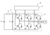
- FIG. 2 shows an outline of the entire power conversion device A according to Embodiment 1 of the present invention.
- This power converter (inverter) A is a device that converts and supplies DC power stored in a power source V such as a battery into multiphase AC power (three phases in this example) for driving the motor M. .
- the power conversion device A includes a power conversion circuit 1 as a power conversion unit and a control device 3.
- the power conversion circuit 1 includes a semiconductor module 2 including a plurality of switch elements S1 to S6, and a smoothing reactor 4 and a smoothing capacitor 5 provided between the power source V and the semiconductor module 2.
- the control device 3 performs pulse width modulation control by PWM control based on a preset carrier frequency fc on the semiconductor module 2 to control on / off of each of the switch elements S1 to S6. Thus, energization is performed to the coils of the respective phases, not shown, of the motor M.
- FIG. 1 is a cross-sectional view showing the structure of the installation portion of the smoothing capacitor 5 in the power converter A.
- the base plate 11 and the cover 12 form a case 10 that houses the smoothing capacitor 5.
- a smoothing capacitor 5 is installed on the base plate 11.
- the smoothing capacitor 5 is provided with a plurality of capacitor elements 51 and 51 inside a main body 50 made of resin.
- the capacitor element 51 is, for example, a film capacitor, and is formed in a flat shape as shown in the figure, whereby the size in the vertical direction (arrow Z direction) in the drawing of the smoothing capacitor 5 can be suppressed.
- the smoothing capacitor 5 is connected to the base plate 11 by a leg member 52 for attaching to the base plate 11. That is, the leg member 52 is on the lower surface 5a of the main body 50 of the smoothing capacitor 5 and on the support portion of the surface in the direction perpendicular to the film flat surface 51a of the capacitor element 51 (the direction of the arrow Z in the figure). 50 is formed integrally.
- the leg member 52 includes bent portions 52a and 52a which are bent at substantially right angles in a crank shape at two intermediate positions.
- a horizontal extending portion that extends in a substantially horizontal direction between the bent portions 52a and 52a and a direction that intersects a direction perpendicular to the film flat surface 51a (Z direction in the drawing). 52b. Therefore, the leg member 52 can set the spring rigidity in the Z direction based on the bending angle of the bent portion 52a, the length of the horizontal extending portion 52b based on the set position, and the cross-sectional area thereof. It is.
- the power conversion device has the effects listed below.
- the power converter of Embodiment 1 is Power conversion means comprising a smoothing capacitor 5 and switch elements S1 to S6; A control device 3 as control means for controlling the operation of the switch elements S1 to S6 using a carrier signal of a predetermined frequency (fc);
- the resonant frequency f0 of the smoothing capacitor 5 is set to be equal to or lower than 1/2 1/2 of the carrier frequency fc that is the frequency of the carrier signal (where 2 1/2 indicates the square root of 2).
- the displacement x of the smoothing capacitor 5 with respect to the excitation force F is maximum at the resonance frequency f0, and when the excitation force F is set to 1 in the frequency range of 2 1/2 ⁇ f0 or more, The displacement x is 1 or less. Therefore, a region where the displacement x is 1 or less when the vibration force F is 1 is referred to as a vibration isolation region. Therefore, by setting the resonance frequency f0 to 1/2 1/2 (2 1/2 is the square root of 2) or less of the carrier frequency fc that is the frequency of the carrier signal, the carrier frequency fc is in this vibration isolation region. included.
- the vibration suppression of the smoothing capacitor 5 can be achieved by setting the resonance frequency f0. Therefore, it is possible to suppress the vibration of the smoothing capacitor 5 without increasing the size of the smoothing capacitor 5 using the large capacitor element 51 or increasing the cost by adding a member for suppressing vibration transmission.
- a power converter can be provided.
- the power converter of Embodiment 1 is The resonance frequency f0 of the smoothing capacitor 5 is a resonance frequency in a direction perpendicular to the film flat surface 51a of the capacitor element 51 built in the smoothing capacitor 5. That is, it has been confirmed by experiments and the like that the vibration of the smoothing capacitor 5 is greatest in the direction perpendicular to the film flat surface 51a of the capacitor element 51 (Z direction in the figure). Therefore, it is possible to suppress the vibration in the direction in which the vibration direction at the time of resonance is the largest, and to efficiently reduce the vibration and noise of the power converter.
- the degree of freedom in adjusting the spring stiffness of the leg member 52 in the vertical direction is increased. Therefore, compared with the case where the leg member 52 is not provided with the rigidity adjusting portion (the bent portion 52a), the degree of freedom in setting the resonance frequency f0 in the direction perpendicular to the film flat surface 51a is increased, and the above 2) The effect of can be obtained more reliably.
- the rigidity adjusting portion includes a bent portion 52a in which a leg member 52 as a connecting member is bent in a direction intersecting a direction (Z direction) perpendicular to the film flat surface 51a as a displacement direction at the resonance frequency f0. It is characterized by being. Therefore, the resonance frequency f0 can be changed by changing the spring rigidity of the leg member 52 depending on the bending condition of the bent portion 52a. In this manner, the resonance frequency f0 can be set by the bent portion 52a that can be easily processed and formed, and the productivity is excellent.
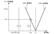
- the negative sideband wave is set so as to be surely in the vibration-proof region when the motor rotation speed is the motor rotation speed Rn1 at which noise that is the muffler is generated. That is, in the second embodiment, the resonance frequency f0 is set to be 1/2 1/2 or less of the frequency fLwr of the negative sideband at the motor rotation speed Rn1. As a result, the frequency fLwr of the negative sideband at the motor rotation speed Rn1 to be muffled is surely included in the vibration isolation region (see FIG. 3), and the vibration of the smoothing capacitor 5 at the motor rotation speed Rn1 is ensured. It can suppress and can reduce reliably the noise used as a muffling object.
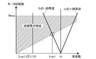
- the third embodiment is a modification of setting the resonance frequency f0 in the Z direction of the film flat surface 51a of the capacitor element 51, and is an example in which noise in a region other than the background noise region is suppressed in the power converter. . That is, since noise generated by the power conversion device is difficult to be heard by the occupant in a region where the background noise is large, the third embodiment suppresses the noise of the power conversion device in a region other than the region where the background noise is large. It is set to.
- the minus sideband is generated on the lower frequency side with respect to the carrier frequency fc.
- the background noise increases as the motor rotation speed increases, so that the noise (noise) of the power converter is masked by the background noise.
- an example of a region where the background noise is large is indicated by hatching. Therefore, in the third embodiment, the resonance frequency f0 intersects the minus sideband of the carrier frequency fc with the region where the background noise of the vehicle is generated that masks the noise of the power converter (large background noise region).
- the frequency was set to be 1/2 1/2 or less of the frequency ffLwr1.
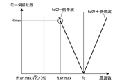
- the fourth embodiment is a modification of setting the resonance frequency f0 in a direction perpendicular to the film flat surface 51a of the capacitor element 51, and is an example of suppressing noise in the entire motor rotation speed in the power converter. That is, in the fourth embodiment, as shown in FIG. 6, the resonance frequency f0 is set to 1/2 1 / of the frequency fLwr_max at which the negative sideband of the carrier frequency fc and the maximum motor rotation speed (maximum motor rotation speed) Rmax intersect. Set to 2 or less. As a result, the carrier frequency fc and the negative sideband can be included in the vibration isolation region in the entire rotation speed range of the motor M, and the noise of the power converter can be more reliably reduced.
- the power conversion device is The resonance frequency f0 in the direction perpendicular to the flat film surface 51a of the smoothing capacitor 5 is 1/2 1/2 or less of the frequency fLwr_max at which the negative sideband of the carrier frequency fc and the maximum motor rotation speed (maximum motor rotation speed) Rmax intersect. It is characterized by being set to. Therefore, the noise of the power conversion device can be reliably reduced in the entire rotation speed range of the motor M.
- Embodiment 5 Next, the power converter of Embodiment 5 is demonstrated based on FIG. 7, FIG.
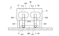
- the fifth embodiment is an example in which a high-power metal bus bar 253 that connects the capacitor element 51 of the smoothing capacitor 205 and the electronic circuit component 200 is provided with a rigidity adjusting portion that is a setting element of the resonance frequency f0. 7 and 8, the cover 12 is not shown.
- the electronic circuit component 200 provided on the base plate 11 and the capacitor element 51 of the smoothing capacitor 205 are electrically connected by a high-voltage bus bar 253.
- the high-power bus bar 253 is fastened to the electronic circuit component 200 with bolts 257 and extends in a direction perpendicular to the film flat surface 51 a (Z direction in the figure) and is connected to the capacitor element 51. ing.
- a bent portion (rigidity adjusting portion) 253a that is bent in the horizontal direction is formed in the middle portion in the longitudinal direction of the high voltage bus bar 253. That is, the high-power bus bar 253 has a bent portion 253a formed in the middle portion thereof, so that the spring rigidity in the direction perpendicular to the film flat surface 51a (the Z direction in the figure) does not provide the bent portion 253a. Has been lowered. In this case, the longer the span of the bent portion 253a in the horizontal direction perpendicular to the Z direction, the lower the spring rigidity of the high-power bus bar 253 and the lower the resonance frequency f0.
- the resonance frequency f0 of the smoothing capacitor 205 and the carrier frequency fc are included in the vibration-proof region as in the first to fifth embodiments. Can be set.
- the spring rigidity of the leg member 252 that attaches the smoothing capacitor 205 to the base plate 11 is set lower than the spring rigidity of the high-voltage bus bar 253. Therefore, it is assumed that the spring rigidity of the high-voltage bus bar 253 contributes to the setting of the resonance frequency f0.
- the power converter of Embodiment 5 The rigidity adjusting portion includes a bent portion 253a in which a high-voltage bus bar 253 as a connecting member is bent in a direction intersecting a direction perpendicular to the film flat surface 51a (Z direction in the drawing). And Therefore, the spring rigidity adjustment of the metal high-voltage bus bar 253 can be easily set based on the bending amount of the bending portion 253a that can be easily processed.
- the sixth embodiment is a modification of the fifth embodiment, and the means for reducing the rigidity in the Z direction of the high voltage bus bar 353 shown in FIG. 9 is different.
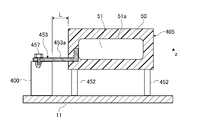
- the power conversion device of the seventh embodiment differs from the fifth and sixth embodiments in the extending direction of the high-power bus bar 453 and the rigidity adjusting means. That is, as shown in FIGS. 10 and 11, in the electronic circuit component 400, the extending direction of the high voltage bus bar 453 connecting the capacitor element 51 of the smoothing capacitor 405 and the electronic circuit component 400 is substantially parallel to the film flat surface 51a.
- Direction (arrow X direction).
- the resonance frequency f0 of the smoothing capacitor 405 is set so that the carrier frequency fc is included in the vibration-proof region by setting the spring rigidity of the high-voltage bus bar 453 based on the length (L) of the horizontal extending portion 453a. be able to.
- the power conversion device is The high-power bus bar 453 serving as a connecting member intersects the displacement direction (direction perpendicular to the film flat surface 51a) at the resonance frequency f0 between the fixed portion with respect to the smoothing capacitor 405 and the fixed portion with respect to the electronic circuit component 400 on the case 10 side.
- the rigidity adjusting portion is configured to be able to adjust the spring rigidity based on the length L of the horizontal extending portion 453a extending in the extending direction. It is characterized by being.
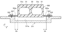
- the leg member 552 extends in a substantially horizontal direction (arrow Y direction) from the main body 50 of the smoothing capacitor 505 and intersects with the Z direction, which is a direction perpendicular to the film flat surface 51a, and the edge of the recess 511a. It is fixed to the part by bolts 557. Further, the leg member 552 constitutes a rigidity adjusting means in which a horizontal extending portion 552a overlapping the concave portion 511a in the Z direction allows the smoothing capacitor 505 to be displaced in the Z direction. That is, as the length of the horizontal extending portion 552a increases, the spring rigidity in the Z direction of the leg member 552 decreases, and the resonance frequency f0 of the smoothing capacitor 505 can be decreased.
- the torque detection apparatus of this invention was demonstrated based on embodiment, about a specific structure, it is not restricted to these embodiment, The summary of the invention which concerns on each claim of a claim As long as they do not deviate, design changes and additions are permitted.
- the example in which the leg member and the high-voltage bus bar are each provided independently as the connecting member provided with the rigidity adjusting unit is shown, but these may be provided in parallel.
- the example in which the bent portion is provided independently as the rigidity adjusting portion and the example in which the narrow-width shaped portion is provided independently are shown, but this bent portion, the narrow-width shaped portion, and The cross direction extending portions may be combined to adjust the rigidity.
- the shape of the high-voltage bus bar shown in the fifth embodiment includes a bent portion and a horizontally extending portion (cross-direction extending portion).
Landscapes
- Engineering & Computer Science (AREA)
- Power Engineering (AREA)
- Inverter Devices (AREA)
Abstract
平滑コンデンサ(5)とスイッチ素子(S1~S6)を備えた電力変換回路(1)と、所定周波数(fc)のキャリア信号を用いてスイッチ素子(S1~S6)の動作を制御する制御手段としての制御装置(3)と、を有し、コンデンサの振動抑制を、低コスト化および省スペース化が可能な手段により達成可能な電力変換装置を提供する。 電力変換回路(1)の平滑コンデンサ(5)の共振周波数(f0)を電力変換回路(1)のスイッチ素子(S1~S6)を制御するキャリア信号の周波数の1/21/2以下に設定したことを特徴とする電力変換装置(A)とした。
Description
本発明は、平滑コンデンサを備えた電力変換装置に関する。
従来、電気自動車などでは、平滑コンデンサおよびスイッチング素子を備えた電力変換装置によりバッテリからの直流電力を交流電力に変換してモータに供給している。また、運転者によるアクセル操作などに応じて電力変換装置のスイッチング素子のスイッチング動作を制御することにより、モータの出力トルクを制御している。
上述の電力変換装置では、スイッチング素子のスイッチング動作に起因して電流脈動が発生し、電流脈動が平滑コンデンサを振動させる原因となっており、また、この平滑コンデンサの振動が騒音を招いていた。
上述の電力変換装置では、スイッチング素子のスイッチング動作に起因して電流脈動が発生し、電流脈動が平滑コンデンサを振動させる原因となっており、また、この平滑コンデンサの振動が騒音を招いていた。
この騒音対策技術として、例えば、平滑コンデンサとして、フィルムを強めのテンションで引っ張って円筒巻形状としたものを用い、扁平巻コンデンサを用いたものと比較して、騒音を低減させるようにした技術が提案されている(例えば、特許文献1参照)。
あるいは、コンデンサを収容するケースと冷却部材との間に防振材を挿入し、コンデンサからケースへの振動伝達を抑制して騒音を低減させるようにした技術も提案されている(例えば、特許文献2参照)。
あるいは、コンデンサを収容するケースと冷却部材との間に防振材を挿入し、コンデンサからケースへの振動伝達を抑制して騒音を低減させるようにした技術も提案されている(例えば、特許文献2参照)。
しかしながら、上記特許文献1に記載の技術のように、円筒巻状のコンデンサを用いた場合、扁平巻のものと比較してコンデンサの体積が大きくなることに伴い、電力変換装置の大きさが肥大化し、重量増およびコスト増を招くという問題点があった。
また、特許文献2に記載の技術のように、防振材を追加した場合にも、部品点数増によるコスト増、重量増、組付工数増を招くという問題点があった
本発明は、上記問題に着目してなされたもので、コンデンサの振動抑制を、低コスト化および省スペース化が可能な手段により達成可能な電力変換装置を提供することを目的とする。
また、特許文献2に記載の技術のように、防振材を追加した場合にも、部品点数増によるコスト増、重量増、組付工数増を招くという問題点があった
本発明は、上記問題に着目してなされたもので、コンデンサの振動抑制を、低コスト化および省スペース化が可能な手段により達成可能な電力変換装置を提供することを目的とする。
上記目的を達成するため、本発明は、電力変換手段の平滑コンデンサの共振周波数を、電力変換手段のスイッチ素子を制御するキャリア信号の周波数の1/21/2以下に設定したことを特徴とする電力変換装置とした。
電力変換装置では、平滑コンデンサに作用する起振力による変位は、共振周波数で最大となり、共振周波数を超える周波数では徐々に低下する。そして、共振周波数に21/2(2の平方根)を乗じた周波数域では、コンデンサの起振力を1とした場合の変位量が1未満となる防振領域となる。
したがって、平滑コンデンサの共振周波数を、キャリア信号の周波数の21/2以下に設定した本発明の電力変換装置では、キャリア周波数は、平滑コンデンサの防振領域に含まれることになる。よって、キャリア信号によりスイッチング素子を駆動させた際の平滑コンデンサの振動を抑えることができる。
このように、本発明の電力変換装置では、平滑コンデンサの共振周波数の設定により、キャリア信号出力時の平滑コンデンサの振動を抑制可能であるため、平滑コンデンサの大型化や追加部品が不要となり、低コスト化および省スペース化が可能となる。
したがって、平滑コンデンサの共振周波数を、キャリア信号の周波数の21/2以下に設定した本発明の電力変換装置では、キャリア周波数は、平滑コンデンサの防振領域に含まれることになる。よって、キャリア信号によりスイッチング素子を駆動させた際の平滑コンデンサの振動を抑えることができる。
このように、本発明の電力変換装置では、平滑コンデンサの共振周波数の設定により、キャリア信号出力時の平滑コンデンサの振動を抑制可能であるため、平滑コンデンサの大型化や追加部品が不要となり、低コスト化および省スペース化が可能となる。
以下、本発明の電力変換装置を実施するための形態を、図面に示す実施の形態に基づいて説明する。
(実施の形態1)
以下に、実施の形態1の電力変換装置について説明する。
図2は、本発明の実施の形態1の電力変換装置Aの全体の概略を示している。
この電力変換装置(インバータ)Aは、バッテリなどの電源Vに蓄積された直流電力を、モータMを駆動するための多相交流電力(この例では3相)に変換して供給する装置である。
(実施の形態1)
以下に、実施の形態1の電力変換装置について説明する。
図2は、本発明の実施の形態1の電力変換装置Aの全体の概略を示している。
この電力変換装置(インバータ)Aは、バッテリなどの電源Vに蓄積された直流電力を、モータMを駆動するための多相交流電力(この例では3相)に変換して供給する装置である。
この電力変換装置Aは、電力変換手段としての電力変換回路1と、制御装置3とを備えている。
電力変換回路1は、複数のスイッチ素子S1~S6を備えた半導体モジュール2と、電源Vと半導体モジュール2の間に設けられた平滑リアクトル4および平滑コンデンサ5と、を備えている。
制御装置3は、半導体モジュール2に対して、あらかじめ設定されたキャリア周波数fcに基づくPWM制御によるパルス幅変調制御を実行して、各スイッチ素子S1~S6のオン、オフを制御する。これにより、モータMの図示を省略した各相のコイルに通電を行なう。
電力変換回路1は、複数のスイッチ素子S1~S6を備えた半導体モジュール2と、電源Vと半導体モジュール2の間に設けられた平滑リアクトル4および平滑コンデンサ5と、を備えている。
制御装置3は、半導体モジュール2に対して、あらかじめ設定されたキャリア周波数fcに基づくPWM制御によるパルス幅変調制御を実行して、各スイッチ素子S1~S6のオン、オフを制御する。これにより、モータMの図示を省略した各相のコイルに通電を行なう。
図1は電力変換装置Aにおける平滑コンデンサ5の設置部分の構造を示す断面図である。
実施の形態1の電力変換装置Aは、ベースプレート11およびカバー12により、平滑コンデンサ5を収容するケース10を形成している。
実施の形態1の電力変換装置Aは、ベースプレート11およびカバー12により、平滑コンデンサ5を収容するケース10を形成している。
ベースプレート11には、平滑コンデンサ5が設置されている。この平滑コンデンサ5は、樹脂により形成された本体50の内部に、複数のコンデンサ素子51,51が設けられている。このコンデンサ素子51は、例えば、フィルムコンデンサであり、図示のように扁平形状に形成されており、これにより、平滑コンデンサ5の図において上下方向(矢印Z方向)の寸法を抑えることができる。
平滑コンデンサ5は、ベースプレート11に取り付けるための脚部材52により、ベースプレート11に連結されている。
すなわち、脚部材52は、平滑コンデンサ5の本体50の下面5aであって、コンデンサ素子51のフィルム平坦面51aに対して垂直な方向(図において矢印Zの方向)の面の支持部分に、本体50と一体に形成されている。
すなわち、脚部材52は、平滑コンデンサ5の本体50の下面5aであって、コンデンサ素子51のフィルム平坦面51aに対して垂直な方向(図において矢印Zの方向)の面の支持部分に、本体50と一体に形成されている。
この脚部材52は、図示のように、中間の2箇所にクランク状に略直角に折曲させた折曲部52a,52aを備えている。そして、両折曲部52a,52aの間に、前記のフィルム平坦面51aと垂直な方向(図においてZ方向)に交差する方向であって、略水平方向に延在された水平方向延在部52bを備えている。したがって、脚部材52は、折曲部52aの折曲角度や、その設定位置に基づく水平方向延在部52bの長さおよびその断面積に基づいて、Z方向のばね剛性を設定することが可能である。
次に、平滑コンデンサ5の共振周波数f0の設定について説明する。
平滑コンデンサ5は、その振動はコンデンサ素子51のフィルム平坦面51aと垂直な方向(図においてZ方向)が最も大きいことが、実験等により確認されている。
また、平滑コンデンサ5の脚部材52は、前述のように、Z方向のばね剛性を設定可能な折曲部52a,52aおよび水平方向延在部52bを備えている。したがって、脚部材52のZ方向のばね剛性を変えることにより、平滑コンデンサ5のZ方向の共振周波数f0を変更可能(設定可能)である。
そこで、本実施の形態1では、平滑コンデンサ5のZ方向の共振周波数f0を、キャリア周波数fcの1/21/2以下(なお、21/2は2の平方根である)に設定している。
平滑コンデンサ5は、その振動はコンデンサ素子51のフィルム平坦面51aと垂直な方向(図においてZ方向)が最も大きいことが、実験等により確認されている。
また、平滑コンデンサ5の脚部材52は、前述のように、Z方向のばね剛性を設定可能な折曲部52a,52aおよび水平方向延在部52bを備えている。したがって、脚部材52のZ方向のばね剛性を変えることにより、平滑コンデンサ5のZ方向の共振周波数f0を変更可能(設定可能)である。
そこで、本実施の形態1では、平滑コンデンサ5のZ方向の共振周波数f0を、キャリア周波数fcの1/21/2以下(なお、21/2は2の平方根である)に設定している。
次に、この共振周波数f0の設定について図3に基づいて説明する。
すなわち、ケース10に作用する起振力は、平滑コンデンサ5の起振力Fを1とすると、それに対する変位xは、図3のような挙動を示す。
具体的には、変位xは、共振周波数f0で最大となり、共振周波数f0を超える周波数では徐々に低下する。そして、周波数が、21/2×f0以上の周波数域では、変位xは1未満となり、この1未満の領域が防振領域となる。
すなわち、ケース10に作用する起振力は、平滑コンデンサ5の起振力Fを1とすると、それに対する変位xは、図3のような挙動を示す。
具体的には、変位xは、共振周波数f0で最大となり、共振周波数f0を超える周波数では徐々に低下する。そして、周波数が、21/2×f0以上の周波数域では、変位xは1未満となり、この1未満の領域が防振領域となる。
これを利用して、本実施の形態1では、平滑コンデンサ5の主たる振動方向であるコンデンサ素子51のフィルム平坦面51aと垂直な方向(Z方向)の共振周波数f0を、キャリア周波数fcの1/21/2以下に設定した。これにより、キャリア周波数fcは、図3に示す防振領域に含まれ、キャリア信号によりスイッチ素子S1~S6を駆動させた際の脈動により平滑コンデンサ5が振動した際に、その振動がケース10へ伝達されるのを確実に抑制することができる。
以上説明した本実施の形態1の電力変換装置は、以下に列挙する効果を奏する。
1)実施の形態1の電力変換装置は、
平滑コンデンサ5とスイッチ素子S1~S6を備えた電力変換手段と、
所定周波数(fc)のキャリア信号を用いてスイッチ素子S1~S6の動作を制御する制御手段としての制御装置3と、
を有し、
平滑コンデンサ5の共振周波数f0が、キャリア信号の周波数であるキャリア周波数fcの1/21/2(なお、この21/2は2の平方根を示している)以下に設定されていることを特徴とする。
平滑コンデンサ5の起振力Fに対する変位xは、図3に示すように、共振周波数f0で最大となり、21/2×f0以上の周波数域では、起振力Fを1としたときに、変位xが1以下となる。そこで、この起振力Fを1としたときに変位xが1以下となる領域を、防振領域と称する。
したがって、共振周波数f0を、キャリア信号の周波数であるキャリア周波数fcの1/21/2(21/2は2の平方根)以下に設定することにより、キャリア周波数fcが、この防振領域に含まれる。これにより、キャリア信号によりスイッチ素子S1~S6を駆動させた際の平滑コンデンサ5の変位xが抑えられ、ケース10への振動伝達を確実に抑制することができる。
このように、実施の形態1では、平滑コンデンサ5の振動抑制を、共振周波数f0の設定により達成できる。よって、大型のコンデンサ素子51を用いて平滑コンデンサ5が大型化したり、振動伝達抑制用の部材を追加してコスト増を招いたりすることなしに、平滑コンデンサ5の振動抑制を図ることが可能な電力変換装置を提供することができる。
1)実施の形態1の電力変換装置は、
平滑コンデンサ5とスイッチ素子S1~S6を備えた電力変換手段と、
所定周波数(fc)のキャリア信号を用いてスイッチ素子S1~S6の動作を制御する制御手段としての制御装置3と、
を有し、
平滑コンデンサ5の共振周波数f0が、キャリア信号の周波数であるキャリア周波数fcの1/21/2(なお、この21/2は2の平方根を示している)以下に設定されていることを特徴とする。
平滑コンデンサ5の起振力Fに対する変位xは、図3に示すように、共振周波数f0で最大となり、21/2×f0以上の周波数域では、起振力Fを1としたときに、変位xが1以下となる。そこで、この起振力Fを1としたときに変位xが1以下となる領域を、防振領域と称する。
したがって、共振周波数f0を、キャリア信号の周波数であるキャリア周波数fcの1/21/2(21/2は2の平方根)以下に設定することにより、キャリア周波数fcが、この防振領域に含まれる。これにより、キャリア信号によりスイッチ素子S1~S6を駆動させた際の平滑コンデンサ5の変位xが抑えられ、ケース10への振動伝達を確実に抑制することができる。
このように、実施の形態1では、平滑コンデンサ5の振動抑制を、共振周波数f0の設定により達成できる。よって、大型のコンデンサ素子51を用いて平滑コンデンサ5が大型化したり、振動伝達抑制用の部材を追加してコスト増を招いたりすることなしに、平滑コンデンサ5の振動抑制を図ることが可能な電力変換装置を提供することができる。
2)実施の形態1の電力変換装置は、
平滑コンデンサ5の共振周波数f0は、平滑コンデンサ5に内蔵されたコンデンサ素子51のフィルム平坦面51aと垂直な方向の共振周波数であることを特徴とする。
すなわち、平滑コンデンサ5の振動はコンデンサ素子51のフィルム平坦面51aと垂直な方向(図においてZ方向)が最も大きいことが、実験等により確認されている。したがって、共振の際の振動方向が最も大きい方向の振動抑制を図り、効率的に電力変換装置の振動および騒音の低減を図ることができる。
平滑コンデンサ5の共振周波数f0は、平滑コンデンサ5に内蔵されたコンデンサ素子51のフィルム平坦面51aと垂直な方向の共振周波数であることを特徴とする。
すなわち、平滑コンデンサ5の振動はコンデンサ素子51のフィルム平坦面51aと垂直な方向(図においてZ方向)が最も大きいことが、実験等により確認されている。したがって、共振の際の振動方向が最も大きい方向の振動抑制を図り、効率的に電力変換装置の振動および騒音の低減を図ることができる。
3)実施の形態1の電力変換装置は、
平滑コンデンサ5は、この平滑コンデンサ5を収容するケース10に、連結部材としての脚部材52を介して直接あるいは間接的に連結された状態で設置され、
連結部材としての脚部材52は、共振周波数f0における変位方向(フィルム平坦面51aに対して垂直な方向)の剛性を調節可能な剛性調節部(折曲部52a)を備えていることを特徴とする。
脚部材52に剛性調節部(折曲部52a)を設けたことにより、この剛性調節部(折曲部52a)を備えないものよりも、共振周波数f0における変位方向であるフィルム平坦面51aに対して垂直な方向の脚部材52のばね剛性の調整自由度が高くなる。
したがって、脚部材52に、剛性調節部(折曲部52a)を設けないものと比較して、フィルム平坦面51aに対して垂直な方向の共振周波数f0の設定自由度が高くなり、上記2)の効果をより確実に得ることが可能となる。
平滑コンデンサ5は、この平滑コンデンサ5を収容するケース10に、連結部材としての脚部材52を介して直接あるいは間接的に連結された状態で設置され、
連結部材としての脚部材52は、共振周波数f0における変位方向(フィルム平坦面51aに対して垂直な方向)の剛性を調節可能な剛性調節部(折曲部52a)を備えていることを特徴とする。
脚部材52に剛性調節部(折曲部52a)を設けたことにより、この剛性調節部(折曲部52a)を備えないものよりも、共振周波数f0における変位方向であるフィルム平坦面51aに対して垂直な方向の脚部材52のばね剛性の調整自由度が高くなる。
したがって、脚部材52に、剛性調節部(折曲部52a)を設けないものと比較して、フィルム平坦面51aに対して垂直な方向の共振周波数f0の設定自由度が高くなり、上記2)の効果をより確実に得ることが可能となる。
4)実施の形態1の電力変換装置は、
連結部材として、平滑コンデンサ5をケース10のベースプレート11に取り付けるための脚部材52が含まれていることを特徴とする。
平滑コンデンサ5の共振周波数f0の設定に、平滑コンデンサ5をベースプレート11に取り付けるための脚部材52を利用するようにしたため、新たに共振周波数f0の設定を行うための部材を追加するものと比較して、コスト低減を図ることが可能である。
加えて、実施の形態1では、脚部材52は、平滑コンデンサ5の本体50に一体に形成されているため、製造効率に優れる。
連結部材として、平滑コンデンサ5をケース10のベースプレート11に取り付けるための脚部材52が含まれていることを特徴とする。
平滑コンデンサ5の共振周波数f0の設定に、平滑コンデンサ5をベースプレート11に取り付けるための脚部材52を利用するようにしたため、新たに共振周波数f0の設定を行うための部材を追加するものと比較して、コスト低減を図ることが可能である。
加えて、実施の形態1では、脚部材52は、平滑コンデンサ5の本体50に一体に形成されているため、製造効率に優れる。
5)実施の形態1の電力変換装置は、
剛性調節部は、連結部材としての脚部材52を、共振周波数f0における変位方向としてのフィルム平坦面51aに垂直な方向(Z方向)に交差する方向に折曲させた折曲部52aを備えていることを特徴とする。
したがって、折曲部52aの曲げ具合などにより、脚部材52のばね剛性を変更して上記共振周波数f0を変更することができる。このように、加工や形成が容易な折曲部52aにより共振周波数f0の設定が可能であり、製造性に優れる。
剛性調節部は、連結部材としての脚部材52を、共振周波数f0における変位方向としてのフィルム平坦面51aに垂直な方向(Z方向)に交差する方向に折曲させた折曲部52aを備えていることを特徴とする。
したがって、折曲部52aの曲げ具合などにより、脚部材52のばね剛性を変更して上記共振周波数f0を変更することができる。このように、加工や形成が容易な折曲部52aにより共振周波数f0の設定が可能であり、製造性に優れる。
6)実施の形態1の電力変換装置は、
連結部材としての脚部材52は、平滑コンデンサ5に対する固定部とベースプレート11に対する固定部との間で、共振周波数f0における変位方向としてのフィルム平坦面51aに垂直な方向(Z方向)に交差する方向に延在された交差方向延在部としての水平方向延在部52bを備え、剛性調節部として、水平方向延在部52bの延在方向の長さに基づいて剛性を調節可能な構成であることを特徴とする。
すなわち、水平方向延在部52bが長くなるほど、脚部材52のZ方向のばね剛性を低下させることができ、この水平方向延在部52bの長さを任意に設定することにより、脚部材52のばね剛性を調節可能である。
よって、共振周波数f0の設定自由度が向上する。また、これにより上記1)2)の効果をさらに確実に得ることが可能となる。
連結部材としての脚部材52は、平滑コンデンサ5に対する固定部とベースプレート11に対する固定部との間で、共振周波数f0における変位方向としてのフィルム平坦面51aに垂直な方向(Z方向)に交差する方向に延在された交差方向延在部としての水平方向延在部52bを備え、剛性調節部として、水平方向延在部52bの延在方向の長さに基づいて剛性を調節可能な構成であることを特徴とする。
すなわち、水平方向延在部52bが長くなるほど、脚部材52のZ方向のばね剛性を低下させることができ、この水平方向延在部52bの長さを任意に設定することにより、脚部材52のばね剛性を調節可能である。
よって、共振周波数f0の設定自由度が向上する。また、これにより上記1)2)の効果をさらに確実に得ることが可能となる。
(他の実施の形態)
次に、他の実施の形態の電力変換装置について説明する。
なお、他の実施の形態は、実施の形態1の変形例であるため、実施の形態1と共通する構成には実施の形態1と同じ符号を付して説明を省略し、実施の形態1との相違点のみ説明する。
次に、他の実施の形態の電力変換装置について説明する。
なお、他の実施の形態は、実施の形態1の変形例であるため、実施の形態1と共通する構成には実施の形態1と同じ符号を付して説明を省略し、実施の形態1との相違点のみ説明する。
(実施の形態2)
実施の形態2の電力変換装置は、コンデンサ素子51のフィルム平坦面51aと垂直な方向であるZ方向の共振周波数f0の設定の変形例であり、電力変換装置において所定のモータ騒音を抑制する例である。
ここで、消音対象となるモータ騒音は、モータ回転数(回転速度)が図4に示すRn1のときに発生する騒音である。
実施の形態2の電力変換装置は、コンデンサ素子51のフィルム平坦面51aと垂直な方向であるZ方向の共振周波数f0の設定の変形例であり、電力変換装置において所定のモータ騒音を抑制する例である。
ここで、消音対象となるモータ騒音は、モータ回転数(回転速度)が図4に示すRn1のときに発生する騒音である。
図4に示すように、キャリア周波数fcは、それぞれ-側帯波および+側帯波を備えている。ここで、+側帯波は、キャリア周波数fcよりも高周波であるため、共振周波数f0を、キャリア周波数fcの1/21/2以下に設定すれば、確実に実施の形態1で説明した防振領域に存在し、この+側帯波による平滑コンデンサ5の振動は抑制される。
一方、-側帯波は、キャリア周波数fcよりも低周波数であるため、モータ回転数が高回転となる周波数領域では、防振領域よりも低周波数となるおそれがある。
一方、-側帯波は、キャリア周波数fcよりも低周波数であるため、モータ回転数が高回転となる周波数領域では、防振領域よりも低周波数となるおそれがある。
そこで、実施の形態2では、モータ回転数が消音対象となる騒音が発生するモータ回転数Rn1のときの-側帯波が、確実に防振領域となるように設定している。
すなわち、実施の形態2では、共振周波数f0を、モータ回転数Rn1のときの-側帯波の周波数fLwrの1/21/2以下となるように設定している。
これにより、消音対象となるモータ回転数Rn1のときの-側帯波の周波数fLwrが確実に防振領域(図3参照)に含まれ、モータ回転数Rn1のときの平滑コンデンサ5の振動を確実に抑制して、消音対象となる騒音を確実に低減できる。
すなわち、実施の形態2では、共振周波数f0を、モータ回転数Rn1のときの-側帯波の周波数fLwrの1/21/2以下となるように設定している。
これにより、消音対象となるモータ回転数Rn1のときの-側帯波の周波数fLwrが確実に防振領域(図3参照)に含まれ、モータ回転数Rn1のときの平滑コンデンサ5の振動を確実に抑制して、消音対象となる騒音を確実に低減できる。
2-1)実施の形態2の電力変換装置は、
平滑コンデンサ5のフィルム平坦面51aと垂直な方向(図1のZ方向)の共振周波数f0が、キャリア信号の周波数(fc)の-側帯波と消音対象のモータ回転速度(モータ回転数Rn1)とが交わる周波数fLwrの1/21/2以下に設定されていることを特徴とする。
したがって、キャリア周波数fcの-側帯波と消音対象のモータ回転数Rn1とが交わる周波数fLwrを防振域に設定することで、モータ回転数Rn1にて生じる騒音を確実に抑制することができる。
平滑コンデンサ5のフィルム平坦面51aと垂直な方向(図1のZ方向)の共振周波数f0が、キャリア信号の周波数(fc)の-側帯波と消音対象のモータ回転速度(モータ回転数Rn1)とが交わる周波数fLwrの1/21/2以下に設定されていることを特徴とする。
したがって、キャリア周波数fcの-側帯波と消音対象のモータ回転数Rn1とが交わる周波数fLwrを防振域に設定することで、モータ回転数Rn1にて生じる騒音を確実に抑制することができる。
(実施の形態3)
実施の形態3は、コンデンサ素子51のフィルム平坦面51aのZ方向の共振周波数f0の設定の変形例であり、電力変換装置において暗騒音領域を除く領域の騒音を抑制するようにした例である。
すなわち、走行時の暗騒音が大きな領域では電力変換装置による騒音が乗員に聞き取られにくいため、実施の形態3では、この暗騒音の大きい領域を除いた領域で電力変換装置の騒音を抑制するように設定している。
実施の形態3は、コンデンサ素子51のフィルム平坦面51aのZ方向の共振周波数f0の設定の変形例であり、電力変換装置において暗騒音領域を除く領域の騒音を抑制するようにした例である。
すなわち、走行時の暗騒音が大きな領域では電力変換装置による騒音が乗員に聞き取られにくいため、実施の形態3では、この暗騒音の大きい領域を除いた領域で電力変換装置の騒音を抑制するように設定している。
図5に示すように、キャリア周波数fcに対して-側帯波は、より低周波数側に発生する。一方、モータ回転数の上昇に伴い、暗騒音が増加することにより電力変換装置のノイズ(騒音)は、暗騒音にマスクされる。
なお、図5では、暗騒音が大きな領域の一例を斜線にて示している。
そこで、実施の形態3では、共振周波数f0が、キャリア周波数fcの-側帯波と、電力変換装置の騒音がマスクされる大きさの車両暗騒音が発生する領域(暗騒音大領域)とが交わる周波数ffLwr1の1/21/2以下となるように設定した。
なお、図5では、暗騒音が大きな領域の一例を斜線にて示している。
そこで、実施の形態3では、共振周波数f0が、キャリア周波数fcの-側帯波と、電力変換装置の騒音がマスクされる大きさの車両暗騒音が発生する領域(暗騒音大領域)とが交わる周波数ffLwr1の1/21/2以下となるように設定した。
したがって、実施の形態3では、電力変換装置の騒音がマスクされない暗騒音大領域以外で、キャリア周波数fcおよびその+側帯波および-側帯波を、防振領域に含むことができ、電力変換装置の騒音をより確実に低減することができる。
また、暗騒音大領域の騒音低減を図らないようにすることにより、平滑コンデンサ5の共振周波数f0の設定範囲が狭まり、より実現が容易となる。
また、暗騒音大領域の騒音低減を図らないようにすることにより、平滑コンデンサ5の共振周波数f0の設定範囲が狭まり、より実現が容易となる。
3-1) 実施の形態3の電力変換装置は、
平滑コンデンサ5のフィルム平坦面51aと垂直な方向(図1のZ方向)の共振周波数f0が、キャリア周波数fcの-側帯波と、所定の大きさの車両暗騒音が発生する領域(暗騒音大領域)とが交わる周波数の1/21/2以下に設定されていることを特徴とする。
これにより、電力変換装置の騒音が暗騒音にマスクされない領域で、キャリア周波数fcおよびその+側帯波および-側帯波を防振領域(図3参照)に含むことができ、電力変換装置の騒音のうち暗騒音大領域に含まれない騒音を効果的に低減することができる。
平滑コンデンサ5のフィルム平坦面51aと垂直な方向(図1のZ方向)の共振周波数f0が、キャリア周波数fcの-側帯波と、所定の大きさの車両暗騒音が発生する領域(暗騒音大領域)とが交わる周波数の1/21/2以下に設定されていることを特徴とする。
これにより、電力変換装置の騒音が暗騒音にマスクされない領域で、キャリア周波数fcおよびその+側帯波および-側帯波を防振領域(図3参照)に含むことができ、電力変換装置の騒音のうち暗騒音大領域に含まれない騒音を効果的に低減することができる。
(実施の形態4)
実施の形態4は、コンデンサ素子51のフィルム平坦面51aと垂直な方向の共振周波数f0の設定の変形例であり、電力変換装置においてモータ回転数の全域の騒音を抑制する例である。
すなわち、実施の形態4では、共振周波数f0を、図6に示すように、キャリア周波数fcの-側帯波と最大モータ回転数(最大モータ回転速度)Rmaxとが交わる周波数fLwr_maxの1/21/2以下に設定した。
これにより、モータMの全回転数域で、キャリア周波数fcおよび-側帯波を、防振領域に含むことができ、電力変換装置の騒音を、より確実に低減することができる。
実施の形態4は、コンデンサ素子51のフィルム平坦面51aと垂直な方向の共振周波数f0の設定の変形例であり、電力変換装置においてモータ回転数の全域の騒音を抑制する例である。
すなわち、実施の形態4では、共振周波数f0を、図6に示すように、キャリア周波数fcの-側帯波と最大モータ回転数(最大モータ回転速度)Rmaxとが交わる周波数fLwr_maxの1/21/2以下に設定した。
これにより、モータMの全回転数域で、キャリア周波数fcおよび-側帯波を、防振領域に含むことができ、電力変換装置の騒音を、より確実に低減することができる。
4-1) 実施の形態4の電力変換装置は、
平滑コンデンサ5のフィルム平坦面51aと垂直な方向の共振周波数f0が、キャリア周波数fcの-側帯波と最大モータ回転数(最大モータ回転速度)Rmaxとが交わる周波数fLwr_maxの1/21/2以下に設定されていることを特徴とする。
したがって、モータMの全回転数域で、電力変換装置の騒音を、確実に低減することができる。
平滑コンデンサ5のフィルム平坦面51aと垂直な方向の共振周波数f0が、キャリア周波数fcの-側帯波と最大モータ回転数(最大モータ回転速度)Rmaxとが交わる周波数fLwr_maxの1/21/2以下に設定されていることを特徴とする。
したがって、モータMの全回転数域で、電力変換装置の騒音を、確実に低減することができる。
(実施の形態5)
次に、実施の形態5の電力変換装置について、図7、図8に基づいて説明する。
この実施の形態5は、平滑コンデンサ205のコンデンサ素子51と電子回路部品200とを接続する金属製の強電バスバー253に、共振周波数f0の設定要素である剛性調節部を持たせた例である。なお、図7、図8において、カバー12は、図示を省略している。
次に、実施の形態5の電力変換装置について、図7、図8に基づいて説明する。
この実施の形態5は、平滑コンデンサ205のコンデンサ素子51と電子回路部品200とを接続する金属製の強電バスバー253に、共振周波数f0の設定要素である剛性調節部を持たせた例である。なお、図7、図8において、カバー12は、図示を省略している。
図7、図8に示すように、ベースプレート11に設けられた電子回路部品200と、平滑コンデンサ205のコンデンサ素子51とが、強電バスバー253により電気的に接続されている。この強電バスバー253は、電子回路部品200に対しボルト257により締結されており、かつ、フィルム平坦面51aに対して垂直な方向(図中Z方向)に延在されて、コンデンサ素子51に接続されている。
さらに、強電バスバー253の長手方向中間部には、図8に示すように、水平方向に凸状に折曲された折曲部(剛性調節部)253aが形成されている。すなわち、強電バスバー253は、その中間部に折曲部253aを形成することにより、フィルム平坦面51aに対して垂直な方向(図中Z方向)に対するばね剛性が、折曲部253aを設けないものよりも低下されている。この場合、折曲部253aの、Z方向に直交する水平方向のスパンを長くするほど、強電バスバー253のばね剛性が低下し、共振周波数f0を低下させることが可能である。
そして、この折曲部253aによる強電バスバー253の曲げ剛性の設定により、平滑コンデンサ205の共振周波数f0を、実施の形態1~実施の形態5と同様に、キャリア周波数fcが、防振領域に含まれるように設定することができる。
なお、この実施の形態5では、平滑コンデンサ205をベースプレート11に取り付ける脚部材252のばね剛性は、強電バスバー253のばね剛性に比べて、低く設定されている。したがって、上記の共振周波数f0の設定には、強電バスバー253のばね剛性が寄与しているものとする。
なお、この実施の形態5では、平滑コンデンサ205をベースプレート11に取り付ける脚部材252のばね剛性は、強電バスバー253のばね剛性に比べて、低く設定されている。したがって、上記の共振周波数f0の設定には、強電バスバー253のばね剛性が寄与しているものとする。
5-1) 実施の形態5の電力変換装置は、
連結部材として、コンデンサ素子51に電気的に接続された強電バスバー253が含まれていることを特徴とする。
電気的に接続される強電バスバー253に、剛性調節部としての機能を持たせることにより、平滑コンデンサ205が強電バスバー253によりベースプレート11側に接続されていても、平滑コンデンサ205の共振周波数f0の設定が可能となる。
連結部材として、コンデンサ素子51に電気的に接続された強電バスバー253が含まれていることを特徴とする。
電気的に接続される強電バスバー253に、剛性調節部としての機能を持たせることにより、平滑コンデンサ205が強電バスバー253によりベースプレート11側に接続されていても、平滑コンデンサ205の共振周波数f0の設定が可能となる。
5-2) 実施の形態5の電力変換装置は、
剛性調節部は、連結部材としての強電バスバー253を、フィルム平坦面51aに対して垂直な方向(図中Z方向)に交差する方向に折曲させた折曲部253aを備えていることを特徴とする。
したがって、金属製の強電バスバー253のばね剛性調節を、加工容易な折曲部253aの折曲量に基づいて容易に設定可能である。
剛性調節部は、連結部材としての強電バスバー253を、フィルム平坦面51aに対して垂直な方向(図中Z方向)に交差する方向に折曲させた折曲部253aを備えていることを特徴とする。
したがって、金属製の強電バスバー253のばね剛性調節を、加工容易な折曲部253aの折曲量に基づいて容易に設定可能である。
(実施の形態6)
実施の形態6は、実施の形態5の変形例であり、図9に示す強電バスバー353のZ方向の剛性を低下させる手段が異なる。
実施の形態6は、実施の形態5の変形例であり、図9に示す強電バスバー353のZ方向の剛性を低下させる手段が異なる。
強電バスバー353は、Z方向の中間部に、その断面積を、Z方向に交差する方向(水平方向)に減少させた剛性調節部としての狭幅形状部353aを備えている。すなわち、この狭幅形状部353aの幅を狭くするほど、ばね剛性が低下し、共振周波数f0を低下させることが可能である。
したがって、この狭幅形状部353aによる強電バスバー353のばね剛性の設定により、平滑コンデンサ205の共振周波数f0を、実施の形態1~実施の形態5と同様に、キャリア周波数fcが、防振領域に含まれるように設定することができる。
なお、この実施の形態6にあっても、平滑コンデンサ205をベースプレート11に取り付ける脚部材352のばね剛性は、強電バスバー353のばね剛性に比べて、低く設定されている。
したがって、この狭幅形状部353aによる強電バスバー353のばね剛性の設定により、平滑コンデンサ205の共振周波数f0を、実施の形態1~実施の形態5と同様に、キャリア周波数fcが、防振領域に含まれるように設定することができる。
なお、この実施の形態6にあっても、平滑コンデンサ205をベースプレート11に取り付ける脚部材352のばね剛性は、強電バスバー353のばね剛性に比べて、低く設定されている。
6-1) 実施の形態6の電力変換装置は、
剛性調節部は、連結部材としての強電バスバー353の断面積を、変位方向であるフィルム平坦面51aに対して垂直な方向(図中Z方向)に交差する方向に縮小させた狭幅形状部353aを備えていることを特徴とする。
したがって、金属製の強電バスバー253のばね剛性調節を、加工容易な狭幅形状部353aにおける断面積変化に基づいて容易に設定可能である。これにより、共振周波数f0の設定を容易に行うことができる。
剛性調節部は、連結部材としての強電バスバー353の断面積を、変位方向であるフィルム平坦面51aに対して垂直な方向(図中Z方向)に交差する方向に縮小させた狭幅形状部353aを備えていることを特徴とする。
したがって、金属製の強電バスバー253のばね剛性調節を、加工容易な狭幅形状部353aにおける断面積変化に基づいて容易に設定可能である。これにより、共振周波数f0の設定を容易に行うことができる。
(実施の形態7)
実施の形態7の電力変換装置は、図10、図11に示すように、強電バスバー453の延在方向および剛性調節手段が、実施の形態5,6と異なる。
すなわち、図10、図11に示すように、電子回路部品400は、平滑コンデンサ405のコンデンサ素子51と電子回路部品400とを接続する強電バスバー453の延在方向が、フィルム平坦面51aと略平行な方向(矢印X方向)となっている。
実施の形態7の電力変換装置は、図10、図11に示すように、強電バスバー453の延在方向および剛性調節手段が、実施の形態5,6と異なる。
すなわち、図10、図11に示すように、電子回路部品400は、平滑コンデンサ405のコンデンサ素子51と電子回路部品400とを接続する強電バスバー453の延在方向が、フィルム平坦面51aと略平行な方向(矢印X方向)となっている。
電子回路部品400は、その上面が、コンデンサ素子51の下側のフィルム平坦面51aと略同じ高さに配置される形状および大きさに形成されている。
強電バスバー453は、電子回路部品400にボルト457により締結され、フィルム平坦面51aに垂直な方向と交差する方向である略水平に延在されて、コンデンサ素子51に接続されている。
強電バスバー453は、電子回路部品400にボルト457により締結され、フィルム平坦面51aに垂直な方向と交差する方向である略水平に延在されて、コンデンサ素子51に接続されている。
この強電バスバー453は、この電子回路部品400への固定部とコンデンサ素子51への固定部との間で水平方向に延在された水平方向延在部453aの長さ(L)に基づいて、Z方向のばね剛性が設定される。すなわち、この水平方向延在部453aの長さ(L)が長くなるほどばね剛性が低下し、短くなるほどばね剛性が上昇する。よって、このばね剛性の調節に基づいて共振周波数f0を設定することができる。なお、強電バスバー453と並列に平滑コンデンサ405とベースプレート11との間に設けられた脚部材452は、Z方向のばね剛性が強電バスバー453よりも低く設定されているものとする。
したがって、この水平方向延在部453aの長さ(L)に基づく強電バスバー453のばね剛性の設定により、平滑コンデンサ405の共振周波数f0を、キャリア周波数fcが防振領域に含まれるように設定することができる。
したがって、この水平方向延在部453aの長さ(L)に基づく強電バスバー453のばね剛性の設定により、平滑コンデンサ405の共振周波数f0を、キャリア周波数fcが防振領域に含まれるように設定することができる。
7-1) 実施の形態7の電力変換装置は、
連結部材としての強電バスバー453は、平滑コンデンサ405に対する固定部とケース10側の電子回路部品400に対する固定部との間で、共振周波数f0における変位方向(フィルム平坦面51aに垂直な方向)に交差する方向(Z方向)である略水平方向に延在され、剛性調節部は、この延在方向に延在された水平方向延在部453aの長さLに基づいてばね剛性を調節可能な構成であることを特徴とする。
したがって、強電バスバー453におけるZ方向への変位が許容された水平方向延在部453aの長さLに基づくばね剛性の設定により、共振周波数f0を設定することができ、共振周波数f0の設定が容易である。
連結部材としての強電バスバー453は、平滑コンデンサ405に対する固定部とケース10側の電子回路部品400に対する固定部との間で、共振周波数f0における変位方向(フィルム平坦面51aに垂直な方向)に交差する方向(Z方向)である略水平方向に延在され、剛性調節部は、この延在方向に延在された水平方向延在部453aの長さLに基づいてばね剛性を調節可能な構成であることを特徴とする。
したがって、強電バスバー453におけるZ方向への変位が許容された水平方向延在部453aの長さLに基づくばね剛性の設定により、共振周波数f0を設定することができ、共振周波数f0の設定が容易である。
(実施の形態8)
実施の形態8の電力変換装置は、実施の形態1の変形例であり、図12に示す平滑コンデンサ505と一体の脚部材552,552における剛性調節手段が、実施の形態1と異なる。
実施の形態8の電力変換装置は、実施の形態1の変形例であり、図12に示す平滑コンデンサ505と一体の脚部材552,552における剛性調節手段が、実施の形態1と異なる。
実施の形態8では、図12に示すように、ベースプレート511に凹部511aを形成して、平滑コンデンサ505の振動用のスペースが確保されている。すなわち、凹部511aは、図において上方から見下ろして平面視で、平滑コンデンサ505の本体50よりも広い面積に形成されている。なお、凹部511aの図における上下方向(Z方向)寸法は、図では強調して表示しており、平滑コンデンサ505の振動の際の実際の変位量は極僅かであるため、実際には微小な凹みに形成されている。
脚部材552は、平滑コンデンサ505の本体50からフィルム平坦面51aに垂直な方向であるZ方向と交差する方向であって、略水平方向(矢印Y方向)に延在されて、凹部511aの縁部にボルト557により固定されている。
また、脚部材552は、凹部511aとZ方向で重なる水平方向延在部552aが、平滑コンデンサ505のZ方向の変位を許容する剛性調節手段を構成している。すなわち、この水平方向延在部552aの長さが長くなるほど脚部材552のZ方向のばね剛性が低下し、平滑コンデンサ505の共振周波数f0を低下させることができる。
したがって、脚部材552のベースプレート511側の固定部と平滑コンデンサ505側の固定部の間の水平方向延在部552aの長さLbに基づいて、脚部材552のばね剛性を設定することができる。そして、この脚部材552のばね剛性の設定により、平滑コンデンサ505の共振周波数f0を、キャリア周波数fcが防振領域に含まれるように設定することができる。
また、脚部材552は、凹部511aとZ方向で重なる水平方向延在部552aが、平滑コンデンサ505のZ方向の変位を許容する剛性調節手段を構成している。すなわち、この水平方向延在部552aの長さが長くなるほど脚部材552のZ方向のばね剛性が低下し、平滑コンデンサ505の共振周波数f0を低下させることができる。
したがって、脚部材552のベースプレート511側の固定部と平滑コンデンサ505側の固定部の間の水平方向延在部552aの長さLbに基づいて、脚部材552のばね剛性を設定することができる。そして、この脚部材552のばね剛性の設定により、平滑コンデンサ505の共振周波数f0を、キャリア周波数fcが防振領域に含まれるように設定することができる。
8-1) 実施の形態8の電力変換装置は、
連結部材としての脚部材552は、平滑コンデンサ505に対する固定部とベースプレート511に対する固定部との間で、共振周波数f0による変位方向(フィルム平坦面51aに垂直な方向)に交差する方向である水平方向に延在された水平方向延在部552aを備え、剛性調節部は、この水平方向延在部552aの水平方向への延在方向の長さLbに基づいてばね剛性を調節可能な構成であることを特徴とする。
したがって、脚部材552におけるZ方向への変位が許容された水平方向延在部552aの長さLbに基づくばね剛性の設定により、共振周波数f0を設定することができ、共振周波数f0の設定が容易である。
連結部材としての脚部材552は、平滑コンデンサ505に対する固定部とベースプレート511に対する固定部との間で、共振周波数f0による変位方向(フィルム平坦面51aに垂直な方向)に交差する方向である水平方向に延在された水平方向延在部552aを備え、剛性調節部は、この水平方向延在部552aの水平方向への延在方向の長さLbに基づいてばね剛性を調節可能な構成であることを特徴とする。
したがって、脚部材552におけるZ方向への変位が許容された水平方向延在部552aの長さLbに基づくばね剛性の設定により、共振周波数f0を設定することができ、共振周波数f0の設定が容易である。
以上、本発明のトルク検出装置を実施の形態に基づき説明してきたが、具体的な構成については、これらの実施の形態に限られるものではなく、請求の範囲の各請求項に係る発明の要旨を逸脱しない限り、設計の変更や追加等は許容される。
例えば、実施の形態では、剛性調節部を備えた連結部材として、脚部材と強電バスバーとを、それぞれ単独で設けた例を示したが、これらは並列に設けてもよい。
また、実施の形態では、剛性調節部として、折曲部を独立して設けた例と、狭幅形状部を独立した例と、をそれぞれ示したが、この折曲部、狭幅形状部および交差方向延在部は、それぞれを組み合わせて剛性を調節するようにしてもよい。すなわち、交差方向延在部の途中に狭幅形状部や折曲部を設けたり、折曲部の途中に狭幅形状部を設けたりしてもよい。このようにすることにより、ばね剛性の設定自由度が向上する。
また、実施の形態1では、連結部材としての脚部材の2箇所に折曲部を形成し、その中間に水平方向延在部を備えた構造としたが、これに限定されず、脚部材を、実施の形態5のような折曲部を設けた構成としてもよい。逆に、実施の形態5にて示した強電バスバーの形状を、実施の形態1にて示したように、折曲部と水平方向延在部(交差方向延在部)とを備えた形状とすることもできる。
また、交差方向延在部として、略水平方向に延在させた例を示したが、この交差方向延在部の延在方向は、これに限定されず、フィルム平坦面に垂直な方向に交差する方向であれば、水平方向に対して斜めに傾いた方向に延在させてもよい。
例えば、実施の形態では、剛性調節部を備えた連結部材として、脚部材と強電バスバーとを、それぞれ単独で設けた例を示したが、これらは並列に設けてもよい。
また、実施の形態では、剛性調節部として、折曲部を独立して設けた例と、狭幅形状部を独立した例と、をそれぞれ示したが、この折曲部、狭幅形状部および交差方向延在部は、それぞれを組み合わせて剛性を調節するようにしてもよい。すなわち、交差方向延在部の途中に狭幅形状部や折曲部を設けたり、折曲部の途中に狭幅形状部を設けたりしてもよい。このようにすることにより、ばね剛性の設定自由度が向上する。
また、実施の形態1では、連結部材としての脚部材の2箇所に折曲部を形成し、その中間に水平方向延在部を備えた構造としたが、これに限定されず、脚部材を、実施の形態5のような折曲部を設けた構成としてもよい。逆に、実施の形態5にて示した強電バスバーの形状を、実施の形態1にて示したように、折曲部と水平方向延在部(交差方向延在部)とを備えた形状とすることもできる。
また、交差方向延在部として、略水平方向に延在させた例を示したが、この交差方向延在部の延在方向は、これに限定されず、フィルム平坦面に垂直な方向に交差する方向であれば、水平方向に対して斜めに傾いた方向に延在させてもよい。
本出願は、2013年8月7日に日本国特許庁に出願された特願2013-164326に基づいて優先権を主張し、その全ての開示は完全に本明細書で参照により組み込まれる。
Claims (11)
- 平滑コンデンサとスイッチ素子とを備えた電力変換手段と、
所定周波数のキャリア信号を用いて前記スイッチ素子の動作を制御する制御手段と、
を有し、
前記平滑コンデンサの共振周波数が、前記キャリア信号の周波数の1/21/2以下に設定されていることを特徴とする電力変換装置。 - 請求項1に記載の電力変換装置において、
前記平滑コンデンサの共振周波数は、前記平滑コンデンサに内蔵されたコンデンサ素子のフィルム平坦面と垂直な方向の共振周波数であることを特徴とする電力変換装置。 - 請求項1または請求項2に記載の電力変換装置において、
前記平滑コンデンサの共振周波数が、前記キャリア信号の周波数の-側帯波と消音対象のモータ回転速度とが交わる周波数の1/21/2以下に設定されていることを特徴とする電力変換装置。 - 請求項1または請求項2に記載の電力変換装置において、
前記平滑コンデンサの共振周波数が、キャリア周波数の-側帯波と、所定の大きさの車両暗騒音が発生する領域とが交わる周波数の1/21/2以下に設定されていることを特徴とする電力変換装置。 - 請求項1または請求項2に記載の電力変換装置において、
前記平滑コンデンサの共振周波数が、キャリア周波数の-側帯波と最大モータ回転速度とが交わる周波数の1/21/2以下に設定されていることを特徴とする電力変換装置。 - 請求項1~請求項5のいずれか1項に記載の電力変換装置において、
前記平滑コンデンサは、この平滑コンデンサを収容するケースに、連結部材を介して直接あるいは間接的に連結された状態で設置され、
前記連結部材は、前記共振周波数における前記平滑コンデンサの変位方向の剛性を調節可能な剛性調節部を備えていることを特徴とする電力変換装置。 - 請求項6に記載の電力変換装置において、
前記連結部材として、前記平滑コンデンサを前記ケースに取り付けるための脚部材が含まれていることを特徴とする電力変換装置。 - 請求項6または請求項7に記載の電力変換装置において、
前記連結部材として、前記コンデンサ素子に電気的に接続されたバスバーが含まれていることを特徴とする電力変換装置。 - 請求項6~請求項8のいずれか1項に記載の電力変換装置において、
前記剛性調節部は、前記連結部材を、前記共振周波数における前記平滑コンデンサの変位方向に交差する方向に折曲させた折曲部を備えていることを特徴とする電力変換装置。 - 請求項6~請求項9のいずれか1項に記載の電力変換装置において、
前記剛性調節部は、前記連結部材の断面積を、前記共振周波数における前記平滑コンデンサの変位方向に交差する方向に縮小させた狭幅形状部を備えていることを特徴とする電力変換装置。 - 請求項6~請求項10のいずれか1項に記載の電力変換装置において、
前記連結部材は、前記平滑コンデンサに対する固定部と前記ケースに対する固定部との間で、前記共振周波数における前記平滑コンデンサの変位方向に交差する方向に延在された交差方向延在部を備え、この交差方向延在部の延在方向の長さに基づいて前記剛性を調節可能な構成であることを特徴とする電力変換装置。
Priority Applications (1)
| Application Number | Priority Date | Filing Date | Title |
|---|---|---|---|
| JP2015530742A JP6103062B2 (ja) | 2013-08-07 | 2014-06-18 | 電力変換装置 |
Applications Claiming Priority (2)
| Application Number | Priority Date | Filing Date | Title |
|---|---|---|---|
| JP2013-164326 | 2013-08-07 | ||
| JP2013164326 | 2013-08-07 |
Publications (1)
| Publication Number | Publication Date |
|---|---|
| WO2015019718A1 true WO2015019718A1 (ja) | 2015-02-12 |
Family
ID=52461059
Family Applications (1)
| Application Number | Title | Priority Date | Filing Date |
|---|---|---|---|
| PCT/JP2014/066160 Ceased WO2015019718A1 (ja) | 2013-08-07 | 2014-06-18 | 電力変換装置 |
Country Status (2)
| Country | Link |
|---|---|
| JP (1) | JP6103062B2 (ja) |
| WO (1) | WO2015019718A1 (ja) |
Cited By (1)
| Publication number | Priority date | Publication date | Assignee | Title |
|---|---|---|---|---|
| CN113405754A (zh) * | 2021-05-28 | 2021-09-17 | 国网山东省电力公司营销服务中心(计量中心) | 一种用于电能计量器具的振动试验固定装置及方法 |
Citations (3)
| Publication number | Priority date | Publication date | Assignee | Title |
|---|---|---|---|---|
| JP2002272126A (ja) * | 2001-03-08 | 2002-09-20 | Daikin Ind Ltd | 空調機用インバータ制御方法およびその装置 |
| JP2006304410A (ja) * | 2005-04-18 | 2006-11-02 | Matsushita Electric Ind Co Ltd | モータ駆動制御装置 |
| JP2008252962A (ja) * | 2007-03-29 | 2008-10-16 | Mitsubishi Heavy Ind Ltd | 一体型電動圧縮機 |
Family Cites Families (1)
| Publication number | Priority date | Publication date | Assignee | Title |
|---|---|---|---|---|
| JPH0835711A (ja) * | 1994-07-22 | 1996-02-06 | Hitachi Ltd | インバータ付き空気調和機およびその制御方法 |
-
2014
- 2014-06-18 WO PCT/JP2014/066160 patent/WO2015019718A1/ja not_active Ceased
- 2014-06-18 JP JP2015530742A patent/JP6103062B2/ja active Active
Patent Citations (3)
| Publication number | Priority date | Publication date | Assignee | Title |
|---|---|---|---|---|
| JP2002272126A (ja) * | 2001-03-08 | 2002-09-20 | Daikin Ind Ltd | 空調機用インバータ制御方法およびその装置 |
| JP2006304410A (ja) * | 2005-04-18 | 2006-11-02 | Matsushita Electric Ind Co Ltd | モータ駆動制御装置 |
| JP2008252962A (ja) * | 2007-03-29 | 2008-10-16 | Mitsubishi Heavy Ind Ltd | 一体型電動圧縮機 |
Cited By (2)
| Publication number | Priority date | Publication date | Assignee | Title |
|---|---|---|---|---|
| CN113405754A (zh) * | 2021-05-28 | 2021-09-17 | 国网山东省电力公司营销服务中心(计量中心) | 一种用于电能计量器具的振动试验固定装置及方法 |
| CN113405754B (zh) * | 2021-05-28 | 2022-05-31 | 国网山东省电力公司营销服务中心(计量中心) | 一种用于电能计量器具的振动试验固定装置及方法 |
Also Published As
| Publication number | Publication date |
|---|---|
| JP6103062B2 (ja) | 2017-03-29 |
| JPWO2015019718A1 (ja) | 2017-03-02 |
Similar Documents
| Publication | Publication Date | Title |
|---|---|---|
| CN111817487B (zh) | 驱动装置 | |
| US20130264872A1 (en) | Power conversion apparatus including a plurality of power conversion circuits and filter circuit shared thereby | |
| JP5906971B2 (ja) | モータ駆動装置 | |
| CN103430257B (zh) | 电气设备的壳体 | |
| CN106416044A (zh) | 电力控制单元 | |
| JP5885773B2 (ja) | 電力変換装置 | |
| US20240399883A1 (en) | Vehicle drive device | |
| CN113078777A (zh) | 功率转换装置 | |
| JP2007180225A (ja) | リアクトルの固定構造および電気機器ユニット | |
| JP2023053446A (ja) | 車両駆動装置 | |
| JP6103062B2 (ja) | 電力変換装置 | |
| JP2010273422A (ja) | 電力変換装置 | |
| CN104094505B (zh) | 电动机控制组件 | |
| JP7151621B2 (ja) | 電力変換機 | |
| US12213268B2 (en) | Case and electronic device equipped with the same | |
| JP6312170B2 (ja) | モールドモジュール | |
| JP7574714B2 (ja) | 電力制御ユニット | |
| JP2008117847A (ja) | 電圧変換装置およびこの電圧変換装置を備えた車両 | |
| JP6398305B2 (ja) | 車両用ブラケット | |
| WO2012117477A1 (ja) | 電力変換装置 | |
| CN112260560A (zh) | 电力变换装置 | |
| JP4939512B2 (ja) | 電力変換装置 | |
| JP2005124262A (ja) | リアクトルユニット及び電力変換装置 | |
| JP7578027B2 (ja) | 動力線の接続構造 | |
| KR101765937B1 (ko) | 차량용 알터네이터 |
Legal Events
| Date | Code | Title | Description |
|---|---|---|---|
| 121 | Ep: the epo has been informed by wipo that ep was designated in this application |
Ref document number: 14834975 Country of ref document: EP Kind code of ref document: A1 |
|
| ENP | Entry into the national phase |
Ref document number: 2015530742 Country of ref document: JP Kind code of ref document: A |
|
| NENP | Non-entry into the national phase |
Ref country code: DE |
|
| 122 | Ep: pct application non-entry in european phase |
Ref document number: 14834975 Country of ref document: EP Kind code of ref document: A1 |