WO2015019707A1 - Silicon carbide semiconductor substrate, method for producing same, and method for producing silicon carbide semiconductor device - Google Patents
Silicon carbide semiconductor substrate, method for producing same, and method for producing silicon carbide semiconductor device Download PDFInfo
- Publication number
- WO2015019707A1 WO2015019707A1 PCT/JP2014/065712 JP2014065712W WO2015019707A1 WO 2015019707 A1 WO2015019707 A1 WO 2015019707A1 JP 2014065712 W JP2014065712 W JP 2014065712W WO 2015019707 A1 WO2015019707 A1 WO 2015019707A1
- Authority
- WO
- WIPO (PCT)
- Prior art keywords
- silicon carbide
- carbide semiconductor
- semiconductor substrate
- substrate
- main surface
- Prior art date
Links
- 239000000758 substrate Substances 0.000 title claims abstract description 276
- HBMJWWWQQXIZIP-UHFFFAOYSA-N silicon carbide Chemical compound [Si+]#[C-] HBMJWWWQQXIZIP-UHFFFAOYSA-N 0.000 title claims abstract description 237
- 229910010271 silicon carbide Inorganic materials 0.000 title claims abstract description 226
- 239000004065 semiconductor Substances 0.000 title claims abstract description 222
- 238000004519 manufacturing process Methods 0.000 title claims description 70
- 229910021421 monocrystalline silicon Inorganic materials 0.000 claims abstract description 12
- 238000000034 method Methods 0.000 claims description 52
- 239000012535 impurity Substances 0.000 claims description 41
- 230000003746 surface roughness Effects 0.000 claims description 12
- 238000005498 polishing Methods 0.000 claims description 10
- KRHYYFGTRYWZRS-UHFFFAOYSA-N Fluorane Chemical compound F KRHYYFGTRYWZRS-UHFFFAOYSA-N 0.000 claims description 9
- 238000005530 etching Methods 0.000 claims description 7
- 238000001020 plasma etching Methods 0.000 claims description 7
- 150000002500 ions Chemical class 0.000 claims description 5
- 229910052736 halogen Inorganic materials 0.000 claims description 4
- 150000002367 halogens Chemical class 0.000 claims description 4
- 239000000126 substance Substances 0.000 claims description 2
- 210000000746 body region Anatomy 0.000 description 17
- 238000002513 implantation Methods 0.000 description 15
- 238000005468 ion implantation Methods 0.000 description 15
- 230000005856 abnormality Effects 0.000 description 7
- 239000007789 gas Substances 0.000 description 7
- 238000010438 heat treatment Methods 0.000 description 7
- 230000008569 process Effects 0.000 description 7
- IJGRMHOSHXDMSA-UHFFFAOYSA-N Atomic nitrogen Chemical compound N#N IJGRMHOSHXDMSA-UHFFFAOYSA-N 0.000 description 6
- 230000000694 effects Effects 0.000 description 6
- 238000001179 sorption measurement Methods 0.000 description 6
- XUIMIQQOPSSXEZ-UHFFFAOYSA-N Silicon Chemical compound [Si] XUIMIQQOPSSXEZ-UHFFFAOYSA-N 0.000 description 5
- 238000005336 cracking Methods 0.000 description 5
- 238000010586 diagram Methods 0.000 description 5
- 229910052710 silicon Inorganic materials 0.000 description 5
- 239000010703 silicon Substances 0.000 description 5
- 229910052782 aluminium Inorganic materials 0.000 description 4
- 229910052751 metal Inorganic materials 0.000 description 4
- 239000002184 metal Substances 0.000 description 4
- 229910021420 polycrystalline silicon Inorganic materials 0.000 description 4
- 229920005591 polysilicon Polymers 0.000 description 4
- 235000012431 wafers Nutrition 0.000 description 4
- PXHVJJICTQNCMI-UHFFFAOYSA-N Nickel Chemical compound [Ni] PXHVJJICTQNCMI-UHFFFAOYSA-N 0.000 description 3
- OAICVXFJPJFONN-UHFFFAOYSA-N Phosphorus Chemical compound [P] OAICVXFJPJFONN-UHFFFAOYSA-N 0.000 description 3
- 229910004298 SiO 2 Inorganic materials 0.000 description 3
- XAGFODPZIPBFFR-UHFFFAOYSA-N aluminium Chemical compound [Al] XAGFODPZIPBFFR-UHFFFAOYSA-N 0.000 description 3
- 229910052796 boron Inorganic materials 0.000 description 3
- 239000013078 crystal Substances 0.000 description 3
- 230000006866 deterioration Effects 0.000 description 3
- 229910052757 nitrogen Inorganic materials 0.000 description 3
- 230000002093 peripheral effect Effects 0.000 description 3
- 229910052698 phosphorus Inorganic materials 0.000 description 3
- 239000011574 phosphorus Substances 0.000 description 3
- 239000010936 titanium Substances 0.000 description 3
- XKRFYHLGVUSROY-UHFFFAOYSA-N Argon Chemical compound [Ar] XKRFYHLGVUSROY-UHFFFAOYSA-N 0.000 description 2
- ZOXJGFHDIHLPTG-UHFFFAOYSA-N Boron Chemical compound [B] ZOXJGFHDIHLPTG-UHFFFAOYSA-N 0.000 description 2
- OKTJSMMVPCPJKN-UHFFFAOYSA-N Carbon Chemical compound [C] OKTJSMMVPCPJKN-UHFFFAOYSA-N 0.000 description 2
- ATUOYWHBWRKTHZ-UHFFFAOYSA-N Propane Chemical compound CCC ATUOYWHBWRKTHZ-UHFFFAOYSA-N 0.000 description 2
- VYPSYNLAJGMNEJ-UHFFFAOYSA-N Silicium dioxide Chemical compound O=[Si]=O VYPSYNLAJGMNEJ-UHFFFAOYSA-N 0.000 description 2
- 229910052799 carbon Inorganic materials 0.000 description 2
- 230000008859 change Effects 0.000 description 2
- 239000000460 chlorine Substances 0.000 description 2
- 239000004020 conductor Substances 0.000 description 2
- 230000007547 defect Effects 0.000 description 2
- 239000000463 material Substances 0.000 description 2
- 230000001681 protective effect Effects 0.000 description 2
- ZAMOUSCENKQFHK-UHFFFAOYSA-N Chlorine atom Chemical compound [Cl] ZAMOUSCENKQFHK-UHFFFAOYSA-N 0.000 description 1
- BLRPTPMANUNPDV-UHFFFAOYSA-N Silane Chemical compound [SiH4] BLRPTPMANUNPDV-UHFFFAOYSA-N 0.000 description 1
- RTAQQCXQSZGOHL-UHFFFAOYSA-N Titanium Chemical compound [Ti] RTAQQCXQSZGOHL-UHFFFAOYSA-N 0.000 description 1
- 230000003213 activating effect Effects 0.000 description 1
- 229910052786 argon Inorganic materials 0.000 description 1
- QVGXLLKOCUKJST-UHFFFAOYSA-N atomic oxygen Chemical compound [O] QVGXLLKOCUKJST-UHFFFAOYSA-N 0.000 description 1
- 238000005229 chemical vapour deposition Methods 0.000 description 1
- 229910052801 chlorine Inorganic materials 0.000 description 1
- 230000001771 impaired effect Effects 0.000 description 1
- 230000001939 inductive effect Effects 0.000 description 1
- 239000011261 inert gas Substances 0.000 description 1
- 238000012986 modification Methods 0.000 description 1
- 230000004048 modification Effects 0.000 description 1
- QPJSUIGXIBEQAC-UHFFFAOYSA-N n-(2,4-dichloro-5-propan-2-yloxyphenyl)acetamide Chemical compound CC(C)OC1=CC(NC(C)=O)=C(Cl)C=C1Cl QPJSUIGXIBEQAC-UHFFFAOYSA-N 0.000 description 1
- 229910052759 nickel Inorganic materials 0.000 description 1
- 230000003647 oxidation Effects 0.000 description 1
- 238000007254 oxidation reaction Methods 0.000 description 1
- 239000001301 oxygen Substances 0.000 description 1
- 229910052760 oxygen Inorganic materials 0.000 description 1
- 239000001294 propane Substances 0.000 description 1
- 230000005855 radiation Effects 0.000 description 1
- 239000012495 reaction gas Substances 0.000 description 1
- 229910000077 silane Inorganic materials 0.000 description 1
- SBEQWOXEGHQIMW-UHFFFAOYSA-N silicon Chemical compound [Si].[Si] SBEQWOXEGHQIMW-UHFFFAOYSA-N 0.000 description 1
- 235000012239 silicon dioxide Nutrition 0.000 description 1
- 239000000377 silicon dioxide Substances 0.000 description 1
- 238000004544 sputter deposition Methods 0.000 description 1
- 229910052719 titanium Inorganic materials 0.000 description 1
- 238000007740 vapor deposition Methods 0.000 description 1
Images


Classifications
-
- H—ELECTRICITY
- H01—ELECTRIC ELEMENTS
- H01L—SEMICONDUCTOR DEVICES NOT COVERED BY CLASS H10
- H01L21/00—Processes or apparatus adapted for the manufacture or treatment of semiconductor or solid state devices or of parts thereof
- H01L21/02—Manufacture or treatment of semiconductor devices or of parts thereof
- H01L21/04—Manufacture or treatment of semiconductor devices or of parts thereof the devices having at least one potential-jump barrier or surface barrier, e.g. PN junction, depletion layer or carrier concentration layer
- H01L21/18—Manufacture or treatment of semiconductor devices or of parts thereof the devices having at least one potential-jump barrier or surface barrier, e.g. PN junction, depletion layer or carrier concentration layer the devices having semiconductor bodies comprising elements of Group IV of the Periodic System or AIIIBV compounds with or without impurities, e.g. doping materials
- H01L21/20—Deposition of semiconductor materials on a substrate, e.g. epitaxial growth solid phase epitaxy
-
- H—ELECTRICITY
- H01—ELECTRIC ELEMENTS
- H01L—SEMICONDUCTOR DEVICES NOT COVERED BY CLASS H10
- H01L29/00—Semiconductor devices adapted for rectifying, amplifying, oscillating or switching, or capacitors or resistors with at least one potential-jump barrier or surface barrier, e.g. PN junction depletion layer or carrier concentration layer; Details of semiconductor bodies or of electrodes thereof ; Multistep manufacturing processes therefor
- H01L29/02—Semiconductor bodies ; Multistep manufacturing processes therefor
- H01L29/12—Semiconductor bodies ; Multistep manufacturing processes therefor characterised by the materials of which they are formed
- H01L29/16—Semiconductor bodies ; Multistep manufacturing processes therefor characterised by the materials of which they are formed including, apart from doping materials or other impurities, only elements of Group IV of the Periodic System
- H01L29/1608—Silicon carbide
-
- H—ELECTRICITY
- H01—ELECTRIC ELEMENTS
- H01L—SEMICONDUCTOR DEVICES NOT COVERED BY CLASS H10
- H01L21/00—Processes or apparatus adapted for the manufacture or treatment of semiconductor or solid state devices or of parts thereof
- H01L21/02—Manufacture or treatment of semiconductor devices or of parts thereof
- H01L21/02002—Preparing wafers
-
- H—ELECTRICITY
- H01—ELECTRIC ELEMENTS
- H01L—SEMICONDUCTOR DEVICES NOT COVERED BY CLASS H10
- H01L21/00—Processes or apparatus adapted for the manufacture or treatment of semiconductor or solid state devices or of parts thereof
- H01L21/02—Manufacture or treatment of semiconductor devices or of parts thereof
- H01L21/02104—Forming layers
- H01L21/02107—Forming insulating materials on a substrate
- H01L21/02225—Forming insulating materials on a substrate characterised by the process for the formation of the insulating layer
- H01L21/02227—Forming insulating materials on a substrate characterised by the process for the formation of the insulating layer formation by a process other than a deposition process
- H01L21/0223—Forming insulating materials on a substrate characterised by the process for the formation of the insulating layer formation by a process other than a deposition process formation by oxidation, e.g. oxidation of the substrate
- H01L21/02233—Forming insulating materials on a substrate characterised by the process for the formation of the insulating layer formation by a process other than a deposition process formation by oxidation, e.g. oxidation of the substrate of the semiconductor substrate or a semiconductor layer
- H01L21/02236—Forming insulating materials on a substrate characterised by the process for the formation of the insulating layer formation by a process other than a deposition process formation by oxidation, e.g. oxidation of the substrate of the semiconductor substrate or a semiconductor layer group IV semiconductor
-
- H—ELECTRICITY
- H01—ELECTRIC ELEMENTS
- H01L—SEMICONDUCTOR DEVICES NOT COVERED BY CLASS H10
- H01L21/00—Processes or apparatus adapted for the manufacture or treatment of semiconductor or solid state devices or of parts thereof
- H01L21/02—Manufacture or treatment of semiconductor devices or of parts thereof
- H01L21/02104—Forming layers
- H01L21/02365—Forming inorganic semiconducting materials on a substrate
- H01L21/02367—Substrates
- H01L21/0237—Materials
- H01L21/02373—Group 14 semiconducting materials
- H01L21/02378—Silicon carbide
-
- H—ELECTRICITY
- H01—ELECTRIC ELEMENTS
- H01L—SEMICONDUCTOR DEVICES NOT COVERED BY CLASS H10
- H01L21/00—Processes or apparatus adapted for the manufacture or treatment of semiconductor or solid state devices or of parts thereof
- H01L21/02—Manufacture or treatment of semiconductor devices or of parts thereof
- H01L21/02104—Forming layers
- H01L21/02365—Forming inorganic semiconducting materials on a substrate
- H01L21/02367—Substrates
- H01L21/02428—Structure
-
- H—ELECTRICITY
- H01—ELECTRIC ELEMENTS
- H01L—SEMICONDUCTOR DEVICES NOT COVERED BY CLASS H10
- H01L21/00—Processes or apparatus adapted for the manufacture or treatment of semiconductor or solid state devices or of parts thereof
- H01L21/02—Manufacture or treatment of semiconductor devices or of parts thereof
- H01L21/02104—Forming layers
- H01L21/02365—Forming inorganic semiconducting materials on a substrate
- H01L21/02518—Deposited layers
- H01L21/02521—Materials
- H01L21/02524—Group 14 semiconducting materials
- H01L21/02529—Silicon carbide
-
- H—ELECTRICITY
- H01—ELECTRIC ELEMENTS
- H01L—SEMICONDUCTOR DEVICES NOT COVERED BY CLASS H10
- H01L21/00—Processes or apparatus adapted for the manufacture or treatment of semiconductor or solid state devices or of parts thereof
- H01L21/02—Manufacture or treatment of semiconductor devices or of parts thereof
- H01L21/02104—Forming layers
- H01L21/02365—Forming inorganic semiconducting materials on a substrate
- H01L21/02612—Formation types
- H01L21/02617—Deposition types
- H01L21/0262—Reduction or decomposition of gaseous compounds, e.g. CVD
-
- H—ELECTRICITY
- H01—ELECTRIC ELEMENTS
- H01L—SEMICONDUCTOR DEVICES NOT COVERED BY CLASS H10
- H01L21/00—Processes or apparatus adapted for the manufacture or treatment of semiconductor or solid state devices or of parts thereof
- H01L21/02—Manufacture or treatment of semiconductor devices or of parts thereof
- H01L21/04—Manufacture or treatment of semiconductor devices or of parts thereof the devices having at least one potential-jump barrier or surface barrier, e.g. PN junction, depletion layer or carrier concentration layer
- H01L21/0445—Manufacture or treatment of semiconductor devices or of parts thereof the devices having at least one potential-jump barrier or surface barrier, e.g. PN junction, depletion layer or carrier concentration layer the devices having semiconductor bodies comprising crystalline silicon carbide
- H01L21/0455—Making n or p doped regions or layers, e.g. using diffusion
- H01L21/046—Making n or p doped regions or layers, e.g. using diffusion using ion implantation
- H01L21/047—Making n or p doped regions or layers, e.g. using diffusion using ion implantation characterised by the angle between the ion beam and the crystal planes or the main crystal surface
-
- H—ELECTRICITY
- H01—ELECTRIC ELEMENTS
- H01L—SEMICONDUCTOR DEVICES NOT COVERED BY CLASS H10
- H01L21/00—Processes or apparatus adapted for the manufacture or treatment of semiconductor or solid state devices or of parts thereof
- H01L21/02—Manufacture or treatment of semiconductor devices or of parts thereof
- H01L21/04—Manufacture or treatment of semiconductor devices or of parts thereof the devices having at least one potential-jump barrier or surface barrier, e.g. PN junction, depletion layer or carrier concentration layer
- H01L21/0445—Manufacture or treatment of semiconductor devices or of parts thereof the devices having at least one potential-jump barrier or surface barrier, e.g. PN junction, depletion layer or carrier concentration layer the devices having semiconductor bodies comprising crystalline silicon carbide
- H01L21/0475—Changing the shape of the semiconductor body, e.g. forming recesses
-
- H—ELECTRICITY
- H01—ELECTRIC ELEMENTS
- H01L—SEMICONDUCTOR DEVICES NOT COVERED BY CLASS H10
- H01L21/00—Processes or apparatus adapted for the manufacture or treatment of semiconductor or solid state devices or of parts thereof
- H01L21/02—Manufacture or treatment of semiconductor devices or of parts thereof
- H01L21/04—Manufacture or treatment of semiconductor devices or of parts thereof the devices having at least one potential-jump barrier or surface barrier, e.g. PN junction, depletion layer or carrier concentration layer
- H01L21/18—Manufacture or treatment of semiconductor devices or of parts thereof the devices having at least one potential-jump barrier or surface barrier, e.g. PN junction, depletion layer or carrier concentration layer the devices having semiconductor bodies comprising elements of Group IV of the Periodic System or AIIIBV compounds with or without impurities, e.g. doping materials
- H01L21/20—Deposition of semiconductor materials on a substrate, e.g. epitaxial growth solid phase epitaxy
- H01L21/205—Deposition of semiconductor materials on a substrate, e.g. epitaxial growth solid phase epitaxy using reduction or decomposition of a gaseous compound yielding a solid condensate, i.e. chemical deposition
- H01L21/2053—Expitaxial deposition of elements of Group IV of the Periodic System, e.g. Si, Ge
-
- H—ELECTRICITY
- H01—ELECTRIC ELEMENTS
- H01L—SEMICONDUCTOR DEVICES NOT COVERED BY CLASS H10
- H01L21/00—Processes or apparatus adapted for the manufacture or treatment of semiconductor or solid state devices or of parts thereof
- H01L21/02—Manufacture or treatment of semiconductor devices or of parts thereof
- H01L21/04—Manufacture or treatment of semiconductor devices or of parts thereof the devices having at least one potential-jump barrier or surface barrier, e.g. PN junction, depletion layer or carrier concentration layer
- H01L21/18—Manufacture or treatment of semiconductor devices or of parts thereof the devices having at least one potential-jump barrier or surface barrier, e.g. PN junction, depletion layer or carrier concentration layer the devices having semiconductor bodies comprising elements of Group IV of the Periodic System or AIIIBV compounds with or without impurities, e.g. doping materials
- H01L21/26—Bombardment with radiation
- H01L21/263—Bombardment with radiation with high-energy radiation
- H01L21/265—Bombardment with radiation with high-energy radiation producing ion implantation
- H01L21/26506—Bombardment with radiation with high-energy radiation producing ion implantation in group IV semiconductors
-
- H—ELECTRICITY
- H01—ELECTRIC ELEMENTS
- H01L—SEMICONDUCTOR DEVICES NOT COVERED BY CLASS H10
- H01L21/00—Processes or apparatus adapted for the manufacture or treatment of semiconductor or solid state devices or of parts thereof
- H01L21/02—Manufacture or treatment of semiconductor devices or of parts thereof
- H01L21/04—Manufacture or treatment of semiconductor devices or of parts thereof the devices having at least one potential-jump barrier or surface barrier, e.g. PN junction, depletion layer or carrier concentration layer
- H01L21/18—Manufacture or treatment of semiconductor devices or of parts thereof the devices having at least one potential-jump barrier or surface barrier, e.g. PN junction, depletion layer or carrier concentration layer the devices having semiconductor bodies comprising elements of Group IV of the Periodic System or AIIIBV compounds with or without impurities, e.g. doping materials
- H01L21/30—Treatment of semiconductor bodies using processes or apparatus not provided for in groups H01L21/20 - H01L21/26
- H01L21/302—Treatment of semiconductor bodies using processes or apparatus not provided for in groups H01L21/20 - H01L21/26 to change their surface-physical characteristics or shape, e.g. etching, polishing, cutting
- H01L21/306—Chemical or electrical treatment, e.g. electrolytic etching
- H01L21/30625—With simultaneous mechanical treatment, e.g. mechanico-chemical polishing
-
- H—ELECTRICITY
- H01—ELECTRIC ELEMENTS
- H01L—SEMICONDUCTOR DEVICES NOT COVERED BY CLASS H10
- H01L21/00—Processes or apparatus adapted for the manufacture or treatment of semiconductor or solid state devices or of parts thereof
- H01L21/02—Manufacture or treatment of semiconductor devices or of parts thereof
- H01L21/04—Manufacture or treatment of semiconductor devices or of parts thereof the devices having at least one potential-jump barrier or surface barrier, e.g. PN junction, depletion layer or carrier concentration layer
- H01L21/18—Manufacture or treatment of semiconductor devices or of parts thereof the devices having at least one potential-jump barrier or surface barrier, e.g. PN junction, depletion layer or carrier concentration layer the devices having semiconductor bodies comprising elements of Group IV of the Periodic System or AIIIBV compounds with or without impurities, e.g. doping materials
- H01L21/30—Treatment of semiconductor bodies using processes or apparatus not provided for in groups H01L21/20 - H01L21/26
- H01L21/302—Treatment of semiconductor bodies using processes or apparatus not provided for in groups H01L21/20 - H01L21/26 to change their surface-physical characteristics or shape, e.g. etching, polishing, cutting
- H01L21/306—Chemical or electrical treatment, e.g. electrolytic etching
- H01L21/3065—Plasma etching; Reactive-ion etching
-
- H—ELECTRICITY
- H01—ELECTRIC ELEMENTS
- H01L—SEMICONDUCTOR DEVICES NOT COVERED BY CLASS H10
- H01L21/00—Processes or apparatus adapted for the manufacture or treatment of semiconductor or solid state devices or of parts thereof
- H01L21/02—Manufacture or treatment of semiconductor devices or of parts thereof
- H01L21/04—Manufacture or treatment of semiconductor devices or of parts thereof the devices having at least one potential-jump barrier or surface barrier, e.g. PN junction, depletion layer or carrier concentration layer
- H01L21/18—Manufacture or treatment of semiconductor devices or of parts thereof the devices having at least one potential-jump barrier or surface barrier, e.g. PN junction, depletion layer or carrier concentration layer the devices having semiconductor bodies comprising elements of Group IV of the Periodic System or AIIIBV compounds with or without impurities, e.g. doping materials
- H01L21/30—Treatment of semiconductor bodies using processes or apparatus not provided for in groups H01L21/20 - H01L21/26
- H01L21/31—Treatment of semiconductor bodies using processes or apparatus not provided for in groups H01L21/20 - H01L21/26 to form insulating layers thereon, e.g. for masking or by using photolithographic techniques; After treatment of these layers; Selection of materials for these layers
- H01L21/3105—After-treatment
- H01L21/311—Etching the insulating layers by chemical or physical means
- H01L21/31105—Etching inorganic layers
- H01L21/31111—Etching inorganic layers by chemical means
-
- H—ELECTRICITY
- H01—ELECTRIC ELEMENTS
- H01L—SEMICONDUCTOR DEVICES NOT COVERED BY CLASS H10
- H01L29/00—Semiconductor devices adapted for rectifying, amplifying, oscillating or switching, or capacitors or resistors with at least one potential-jump barrier or surface barrier, e.g. PN junction depletion layer or carrier concentration layer; Details of semiconductor bodies or of electrodes thereof ; Multistep manufacturing processes therefor
- H01L29/02—Semiconductor bodies ; Multistep manufacturing processes therefor
- H01L29/06—Semiconductor bodies ; Multistep manufacturing processes therefor characterised by their shape; characterised by the shapes, relative sizes, or dispositions of the semiconductor regions ; characterised by the concentration or distribution of impurities within semiconductor regions
- H01L29/0603—Semiconductor bodies ; Multistep manufacturing processes therefor characterised by their shape; characterised by the shapes, relative sizes, or dispositions of the semiconductor regions ; characterised by the concentration or distribution of impurities within semiconductor regions characterised by particular constructional design considerations, e.g. for preventing surface leakage, for controlling electric field concentration or for internal isolations regions
- H01L29/0607—Semiconductor bodies ; Multistep manufacturing processes therefor characterised by their shape; characterised by the shapes, relative sizes, or dispositions of the semiconductor regions ; characterised by the concentration or distribution of impurities within semiconductor regions characterised by particular constructional design considerations, e.g. for preventing surface leakage, for controlling electric field concentration or for internal isolations regions for preventing surface leakage or controlling electric field concentration
- H01L29/0611—Semiconductor bodies ; Multistep manufacturing processes therefor characterised by their shape; characterised by the shapes, relative sizes, or dispositions of the semiconductor regions ; characterised by the concentration or distribution of impurities within semiconductor regions characterised by particular constructional design considerations, e.g. for preventing surface leakage, for controlling electric field concentration or for internal isolations regions for preventing surface leakage or controlling electric field concentration for increasing or controlling the breakdown voltage of reverse biased devices
- H01L29/0615—Semiconductor bodies ; Multistep manufacturing processes therefor characterised by their shape; characterised by the shapes, relative sizes, or dispositions of the semiconductor regions ; characterised by the concentration or distribution of impurities within semiconductor regions characterised by particular constructional design considerations, e.g. for preventing surface leakage, for controlling electric field concentration or for internal isolations regions for preventing surface leakage or controlling electric field concentration for increasing or controlling the breakdown voltage of reverse biased devices by the doping profile or the shape or the arrangement of the PN junction, or with supplementary regions, e.g. junction termination extension [JTE]
- H01L29/0619—Semiconductor bodies ; Multistep manufacturing processes therefor characterised by their shape; characterised by the shapes, relative sizes, or dispositions of the semiconductor regions ; characterised by the concentration or distribution of impurities within semiconductor regions characterised by particular constructional design considerations, e.g. for preventing surface leakage, for controlling electric field concentration or for internal isolations regions for preventing surface leakage or controlling electric field concentration for increasing or controlling the breakdown voltage of reverse biased devices by the doping profile or the shape or the arrangement of the PN junction, or with supplementary regions, e.g. junction termination extension [JTE] with a supplementary region doped oppositely to or in rectifying contact with the semiconductor containing or contacting region, e.g. guard rings with PN or Schottky junction
-
- H—ELECTRICITY
- H01—ELECTRIC ELEMENTS
- H01L—SEMICONDUCTOR DEVICES NOT COVERED BY CLASS H10
- H01L29/00—Semiconductor devices adapted for rectifying, amplifying, oscillating or switching, or capacitors or resistors with at least one potential-jump barrier or surface barrier, e.g. PN junction depletion layer or carrier concentration layer; Details of semiconductor bodies or of electrodes thereof ; Multistep manufacturing processes therefor
- H01L29/02—Semiconductor bodies ; Multistep manufacturing processes therefor
- H01L29/12—Semiconductor bodies ; Multistep manufacturing processes therefor characterised by the materials of which they are formed
-
- H—ELECTRICITY
- H01—ELECTRIC ELEMENTS
- H01L—SEMICONDUCTOR DEVICES NOT COVERED BY CLASS H10
- H01L29/00—Semiconductor devices adapted for rectifying, amplifying, oscillating or switching, or capacitors or resistors with at least one potential-jump barrier or surface barrier, e.g. PN junction depletion layer or carrier concentration layer; Details of semiconductor bodies or of electrodes thereof ; Multistep manufacturing processes therefor
- H01L29/66—Types of semiconductor device ; Multistep manufacturing processes therefor
- H01L29/66007—Multistep manufacturing processes
- H01L29/66053—Multistep manufacturing processes of devices having a semiconductor body comprising crystalline silicon carbide
- H01L29/66068—Multistep manufacturing processes of devices having a semiconductor body comprising crystalline silicon carbide the devices being controllable only by the electric current supplied or the electric potential applied, to an electrode which does not carry the current to be rectified, amplified or switched, e.g. three-terminal devices
-
- H—ELECTRICITY
- H01—ELECTRIC ELEMENTS
- H01L—SEMICONDUCTOR DEVICES NOT COVERED BY CLASS H10
- H01L29/00—Semiconductor devices adapted for rectifying, amplifying, oscillating or switching, or capacitors or resistors with at least one potential-jump barrier or surface barrier, e.g. PN junction depletion layer or carrier concentration layer; Details of semiconductor bodies or of electrodes thereof ; Multistep manufacturing processes therefor
- H01L29/66—Types of semiconductor device ; Multistep manufacturing processes therefor
- H01L29/68—Types of semiconductor device ; Multistep manufacturing processes therefor controllable by only the electric current supplied, or only the electric potential applied, to an electrode which does not carry the current to be rectified, amplified or switched
- H01L29/76—Unipolar devices, e.g. field effect transistors
- H01L29/772—Field effect transistors
- H01L29/78—Field effect transistors with field effect produced by an insulated gate
- H01L29/7801—DMOS transistors, i.e. MISFETs with a channel accommodating body or base region adjoining a drain drift region
- H01L29/7802—Vertical DMOS transistors, i.e. VDMOS transistors
- H01L29/7811—Vertical DMOS transistors, i.e. VDMOS transistors with an edge termination structure
-
- H—ELECTRICITY
- H01—ELECTRIC ELEMENTS
- H01L—SEMICONDUCTOR DEVICES NOT COVERED BY CLASS H10
- H01L21/00—Processes or apparatus adapted for the manufacture or treatment of semiconductor or solid state devices or of parts thereof
- H01L21/02—Manufacture or treatment of semiconductor devices or of parts thereof
- H01L21/02104—Forming layers
- H01L21/02107—Forming insulating materials on a substrate
- H01L21/02225—Forming insulating materials on a substrate characterised by the process for the formation of the insulating layer
- H01L21/02227—Forming insulating materials on a substrate characterised by the process for the formation of the insulating layer formation by a process other than a deposition process
- H01L21/02255—Forming insulating materials on a substrate characterised by the process for the formation of the insulating layer formation by a process other than a deposition process formation by thermal treatment
Definitions
- the present invention relates to a silicon carbide semiconductor substrate, a method for manufacturing the same, and a method for manufacturing a silicon carbide semiconductor device, and more particularly, a silicon carbide semiconductor substrate having high flatness even when heat-treated at a high temperature, a method for manufacturing the same, and a silicon carbide semiconductor device. It relates to the manufacturing method.
- SiC silicon carbide
- the silicon carbide semiconductor substrate is being increased in diameter.
- the outer diameter of the silicon carbide semiconductor substrate is, for example, about 6 inches, the flatness of the silicon carbide semiconductor substrate is impaired.
- JP 2012-214376 describes a SiC having a diameter of at least about 75 millimeters (3 inches), a strain of less than about 5 ⁇ m, a warp of less than about 5 mm, and a TTV of less than about 2.0 ⁇ m.
- a wafer is described. Specifically, by slicing the SiC boule into a wafer and starting the lapping process using a downward force that is less than the downward force required to fold the wafer on a double-sided wrapper. It is described that wafers with low distortion, warpage and TTV can be produced.
- the silicon carbide semiconductor substrate whose flatness deteriorates due to heat treatment at a high temperature has been confirmed.
- doping in a method for manufacturing a silicon carbide semiconductor device is performed by ion implantation at a high temperature, but a silicon carbide semiconductor substrate having poor flatness is difficult to be adsorbed on the electrostatic chuck stage of the implantation device. It has been confirmed that problems such as breakage of the substrate may occur depending on the type.
- Such deterioration of flatness at high temperatures is a particularly serious problem in a silicon carbide semiconductor substrate having a large diameter of 100 mm or more. That is, even if a silicon carbide semiconductor substrate having a large diameter (especially 100 mm or more) is used in order to obtain a silicon carbide semiconductor device efficiently, it is difficult to manufacture the silicon carbide semiconductor device with a high yield due to the deterioration of the flatness as described above. Met.
- a main object of the present invention is to provide a silicon carbide semiconductor substrate having high flatness even at high temperatures, a method for manufacturing the same, and a method for manufacturing a silicon carbide semiconductor device.
- Another object of the present invention is to provide a method for manufacturing a silicon carbide semiconductor device capable of manufacturing a silicon carbide semiconductor device with a high yield by using a large-diameter silicon carbide semiconductor substrate.
- Silicon carbide semiconductor substrate 10 has a main surface having an outer diameter of 100 mm or more, and includes a base substrate 1 made of single-crystal silicon carbide and an epitaxial layer 2 formed on main surface 1A. .
- Silicon carbide semiconductor substrate 10 has a warpage amount of ⁇ 100 ⁇ m to 100 ⁇ m when the substrate temperature is room temperature, and a warp amount of ⁇ 1.5 mm to 1.5 mm when the substrate temperature is 400 ° C.
- a method of manufacturing a silicon carbide semiconductor substrate according to the present invention includes a step of preparing a base substrate having a main surface having an outer diameter of 100 mm or more and made of single crystal silicon carbide, and forming an epitaxial layer on the main surface A step of removing at least a part of the back surface of the base substrate opposite to the main surface to prepare a silicon carbide semiconductor substrate; and a step of implanting impurity ions into the silicon carbide semiconductor substrate; Is provided.
- a silicon carbide semiconductor substrate having high flatness even at high temperatures can be obtained.
- FIG. 8 is a reference diagram for illustrating the function and effect of the method for manufacturing the silicon carbide semiconductor device according to the embodiment.
- FIG. 8 is a reference diagram for illustrating the function and effect of the method for manufacturing the silicon carbide semiconductor device according to the embodiment.
- silicon carbide semiconductor substrate 10 has a main surface 2A having an outer diameter of 100 mm or more, a base substrate 1 made of single-crystal silicon carbide, and a main surface 2A, the amount of warpage when the substrate temperature is room temperature is ⁇ 100 ⁇ m or more and 100 ⁇ m or less, and the amount of warpage when the substrate temperature is 400 ° C. is ⁇ 1.5 mm or more and 1 .5 mm or less.
- “warping amount” of silicon carbide semiconductor substrate 10 means main surface 2 ⁇ / b> A of silicon carbide semiconductor substrate 10 when silicon carbide semiconductor substrate 10 is placed on plane S ⁇ b> 1. Is a difference in height between the highest position and the lowest position with respect to the plane S1.
- the amount of warpage is positive or negative when main surface 2A of silicon carbide semiconductor substrate 10 is convex downward (the center position of silicon carbide semiconductor substrate 10 is relative to plane S1 relative to the outer peripheral position).
- the case where it is convex upward is positive.
- “Substrate temperature” is a temperature measured by a radiation thermometer from the main surface 2A side of silicon carbide semiconductor substrate 10, and is measured in a semiconductor manufacturing apparatus such as an ion implantation apparatus, for example.
- Silicon carbide semiconductor substrate 10 according to the present embodiment is a large-diameter substrate having an outer diameter of 100 mm or more, preferably has an outer diameter of 125 mm or more, and more preferably has an outer diameter of 150 mm or more.
- silicon carbide semiconductor substrate 10 is a large-diameter substrate having an outer diameter of 100 mm or more, and a warpage amount when the substrate temperature is 400 ° C. is ⁇ 1.5 mm or more and 1.5 mm or less.
- the flatness is high even at high temperatures.
- doping in the method for manufacturing a silicon carbide semiconductor device is performed by ion implantation into silicon carbide semiconductor substrate 10 at a high temperature, and silicon carbide semiconductor substrate 10 is used as an electrostatic chuck stage of the ion implantation device.
- silicon carbide semiconductor substrate 10 is used as an electrostatic chuck stage of the ion implantation device.
- silicon carbide semiconductor substrate 10 is a large-diameter substrate having an outer diameter of 100 mm or more, and has high flatness even at high temperatures. Therefore, silicon carbide semiconductor substrate 10 is used to form a silicon carbide semiconductor device. When the manufacturing process is advanced, a silicon carbide semiconductor device having a small variation in characteristics can be manufactured on silicon carbide semiconductor substrate 10.
- region) with respect to 2A fluctuate locally within main surface 2A can be suppressed.
- variations in the processing on the main surface 2A can be reduced.
- silicon carbide semiconductor substrate 10 is required to have, for example, an LTV (Local Thickness Variation) of 1 ⁇ m or less in order to perform high-precision exposure.
- LTV Local Thickness Variation
- the silicon carbide semiconductor substrate 10 according to the present embodiment has a small amount of warpage, the apparent LTV does not increase and high-precision exposure can be performed.
- the silicon carbide semiconductor device can be manufactured with high yield by advancing the manufacturing process of the silicon carbide semiconductor device using silicon carbide semiconductor substrate 10 having a large diameter and high flatness.
- base substrate 1 in the direction perpendicular to main surfaces 1A and 2A may have a thickness of 200 ⁇ m or more and 700 ⁇ m or less. Even in this case, silicon carbide semiconductor substrate 10 according to the present embodiment can have a warpage amount of ⁇ 1.5 mm or more and 1.5 mm or less when the substrate temperature is 400 ° C.
- the thickness of epitaxial layer 2 formed on main surface 1A of base substrate 1 is about several ⁇ m or more and 100 ⁇ m or less. Therefore, when base substrate 1 is thin, the amount of warpage of silicon carbide semiconductor substrate 10 increases. On the other hand, when the thickness of the base substrate 1 is thick, the manufacturing cost increases.
- silicon carbide semiconductor substrate 10 according to the present embodiment can have high flatness even at a high temperature even if base substrate 1 does not have a thickness that exceeds 700 ⁇ m. That is, according to the method for manufacturing a silicon carbide substrate in accordance with the present embodiment, silicon carbide semiconductor substrate 10 having high flatness even at high temperatures can be obtained at low cost.
- the surface roughness of back surface 1B located on the opposite side of main surface 2A is preferably 10 nm or less.
- the surface roughness of the back surface 1B of the base substrate 1 is high, for example, silicon (Si) out of silicon carbide constituting the back surface 1B excessively escapes in a high temperature environment, and a carbonized layer (damage layer 3) is formed. It is thought that it is done.
- the inventors have described that a silicon carbide semiconductor substrate in which the surface roughness of the back surface 1B of the base substrate 1 after forming the epitaxial layer 2 on the main surface 1A of the base substrate 1 is 10 nm or less is the substrate temperature as described above.
- the amount of warping when the temperature was 400 ° C. was ⁇ 1.5 mm or more and 1.5 mm or less. That is, one of the causes of the increase in the amount of warp when the substrate temperature of silicon carbide semiconductor substrate 10 is high is the residual strain of damaged layer 3 formed on back surface 1B of base substrate 1 in silicon carbide semiconductor substrate 10. It is presumed that this is due to the stress caused by.
- a method for manufacturing a silicon carbide semiconductor substrate includes a step (S10) of preparing base substrate 1 having a main surface 2A having an outer diameter of 100 mm or more and made of single-crystal silicon carbide; A step (S30) of forming the epitaxial layer 2 on the main surface 2A and a step (S30) of removing at least a part of the back surface 1B located on the opposite side of the main surface 2A in the base substrate 1 are provided.
- the base substrate Part of the back surface 1B of 1 is removed. Thereby, even if the damage layer 3 is formed on the back surface 1B of the base substrate 1 in the step (S20) of forming the epitaxial layer 2, the damage layer 3 is removed in the step (S30) of removing a part of the back surface 1B of the base substrate 1. Removed.
- Silicon carbide semiconductor substrate 10 thus obtained has an outer diameter of 100 mm or more, a warpage amount when the substrate temperature is room temperature, of ⁇ 100 ⁇ m or more and 100 ⁇ m or less, and a substrate temperature of 400 ° C.
- the amount of warpage is not less than ⁇ 1.5 mm and not more than 1.5 mm. That is, according to the method for manufacturing a silicon carbide semiconductor substrate in accordance with the present embodiment, silicon carbide semiconductor substrate 10 having high flatness can be obtained even in an environment of high temperature even if the outer diameter is 100 mm or more.
- the removing step (S30) may be performed by chemically polishing the back surface 1B (Chemical Mechanical Polishing: CMP). Even if it does in this way, even if the damage layer 3 arises in the back surface 1B of the base substrate 1 in the process of forming the epitaxial layer 2 (S20), the damage layer 3 is reliably formed by chemically polishing the back surface 1B of the base substrate 1. Can be removed.
- CMP Chemical Mechanical Polishing
- the removing step (S30) may be performed by reactive ion etching of the back surface 1B. Even if it does in this way, even if the damage layer 3 arises in the back surface 1B of the base substrate 1 in the process (S20) of forming the epitaxial layer 2, the damage layer 3 is formed by reactive ion etching of the back surface 1B of the base substrate 1. It can be removed reliably.
- the removing step (S30) may be performed by thermally etching back surface 1B in a halogen gas atmosphere. Even if it does in this way, even if the damage layer 3 arises in the back surface 1B of the base substrate 1 in the process (S20) of forming the epitaxial layer 2, the damage layer 3 is reliably formed by thermally etching the back surface 1B of the base substrate 1. Can be removed.
- the thermal oxide film is etched using hydrofluoric acid. It may be done by. Even if it does in this way, even if the damage layer 3 arises in the back surface 1B of the base substrate 1 in the process (S20) of forming the epitaxial layer 2, the thermal oxide film formed on the back surface 1B of the base substrate 1 is made of hydrofluoric acid. The damage layer 3 can be reliably removed by using and etching.
- a method for manufacturing a silicon carbide semiconductor device includes a step (S10) of preparing base substrate 1 having a main surface 2A having an outer diameter of 100 mm or more and made of single-crystal silicon carbide; A step of forming epitaxial layer 2 on main surface 2A (S20) and a step of preparing silicon carbide semiconductor substrate 10 by removing at least part of back surface 1B located on the opposite side of main surface 2A in base substrate 1 (S30) and a step of implanting impurity ions into silicon carbide semiconductor substrate 10 (S40).
- the method for manufacturing the silicon carbide semiconductor device according to the present embodiment uses silicon carbide semiconductor substrate 10 obtained by the method for manufacturing the silicon carbide semiconductor substrate according to the present embodiment, and carbonizes on silicon carbide semiconductor substrate 10.
- a silicon semiconductor device is manufactured.
- silicon carbide semiconductor substrate 10 obtained by the method for manufacturing a silicon carbide semiconductor substrate according to the present embodiment has an outer diameter of 100 mm or more and a warpage amount of ⁇ 100 ⁇ m when the substrate temperature is room temperature.
- the amount of warpage when the substrate temperature is 100 ⁇ m or less and the substrate temperature is 400 ° C. is ⁇ 1.5 mm to 1.5 mm.
- the angle formed by the impurity implantation direction with respect to main surface 2A of silicon carbide semiconductor substrate 10 is the main surface of silicon carbide semiconductor substrate 10 even if the outer diameter of silicon carbide semiconductor substrate 10 is 100 mm or more. It can be made substantially constant regardless of the in-plane position of the surface 2A.
- the form of the ion implantation region (for example, the shape of the implantation region in the depth direction of the substrate and the ion concentration profile) can be made substantially constant regardless of the in-plane position of the main surface 2A. Therefore, according to the method for manufacturing the silicon carbide semiconductor device according to the present embodiment, the silicon carbide semiconductor device can be manufactured with a high yield.
- Silicon carbide semiconductor substrate 10 includes a base substrate 1 and an epitaxial layer 2 formed on main surface 1 ⁇ / b> A of base substrate 1.
- Base substrate 1 is made of single crystal silicon carbide and has a main surface 1A having an outer diameter of 6 inches. Silicon carbide constituting base substrate 1 has, for example, a hexagonal crystal structure, and preferably has a crystal polymorph (polytype) of 4H—SiC. Base substrate 1 contains an n-type impurity such as nitrogen (N) at a high concentration, and the conductivity type is n-type.
- the impurity concentration of the base substrate 1 is, for example, about 1.0 ⁇ 10 18 cm ⁇ 3 or more and 1.0 ⁇ 10 18 cm ⁇ 3 or less.
- Main surface 1A may be, for example, a ⁇ 0001 ⁇ plane or a plane having an off angle of 1 ° or more and 10 ° or less with respect to the ⁇ 0001 ⁇ plane.
- the thickness of the base substrate 1 is, for example, about 200 ⁇ m to 700 ⁇ m, preferably 300 ⁇ m to 600 ⁇ m.
- damage layer 3 (see FIG. 6) of carbon and silicon silicon carbide is not formed on back surface 1B located on the opposite side of main surface 1A of base substrate 1. The damage layer 3 will be described later.
- Epitaxial layer 2 is a layer made of silicon carbide formed by epitaxial growth on main surface 1 ⁇ / b> A of base substrate 1.
- Epitaxial layer 2 contains an n-type impurity such as nitrogen (N), for example, and the conductivity type of epitaxial layer 2 is n-type.
- the impurity concentration of the epitaxial layer 2 may be lower than the impurity concentration of the base substrate 1.
- the impurity concentration of the epitaxial layer 2 is, for example, about 7.5 ⁇ 10 15 cm ⁇ 2 .
- the film thickness of the epitaxial layer 2 is, for example, about 5 ⁇ m to 40 ⁇ m.
- the silicon carbide semiconductor substrate 10 has a warpage amount of ⁇ 100 ⁇ m or more and 100 ⁇ m or less, preferably 40 ⁇ m or more and 40 ⁇ m or less when the substrate temperature is room temperature. Further, silicon carbide semiconductor substrate 10 has a warpage amount of ⁇ 1.5 mm to 1.5 mm, preferably ⁇ 1.0 mm to 1.0 mm when the substrate temperature is 100 ° C. to 500 ° C. . More preferably, the amount of warpage when the substrate temperature is 200 ° C. or more and 400 ° C. or less is ⁇ 1.5 mm or more and 1.5 mm or less, and more preferably ⁇ 1.0 mm or more and 1.0 mm or less.
- base substrate 1 having a main surface 1A having an outer diameter of 6 inches and made of single crystal silicon carbide is prepared (step (S10)).
- the base substrate 1 having an outer diameter of 6 inches is prepared by an arbitrary method.
- the outer diameter of the base substrate 1 may be 100 mm or more (for example, 5 inches or 8 inches).
- epitaxial layer 2 is formed on main surface 1A of base substrate 1 by an epitaxial growth method (step (S20)).
- Epitaxial growth is performed by a CVD method.
- the source gas for example, a mixed gas of silane (SiH 4 ) and propane (C 3 H 8 ) can be used.
- nitrogen (N) or phosphorus (P) may be introduced as impurities.
- Layer 3 (carbonized layer) may be formed.
- the damaged layer 3 may be formed with a thickness of about 0.001 ⁇ m or more and 10 ⁇ m or less, for example, and when formed with a thickness of 1 ⁇ m or more, it may be visually confirmed as white turbidity on the back surface 1B.
- the surface roughness (Ra) of the back surface 1B of the region where the damage layer 3 is formed is 0.001 ⁇ m or more.
- the laminate 4 of the base substrate 1 and the epitaxial layer 2 on which the damaged layer 3 is formed on the back surface 1B has warpage when the substrate temperature is room temperature, for example, -150 ⁇ m or more and 150 ⁇ m or less.
- step (S30) at least a part of back surface 1B of base substrate 1 is removed (step (S30)). Specifically, the damage layer 3 is removed by CMP polishing of the back surface 1B of the base substrate 1 in the laminate 4.
- the polishing amount of the back surface 1B of the base substrate 1 is, for example, not less than 0.001 ⁇ m and not more than 10 ⁇ m.
- the surface roughness (Ra) of the back surface 1B after the polishing in this step (S30) is 10 nm or less, preferably 1 nm or less.
- Silicon carbide semiconductor substrate 10 has a back surface of laminate 4 in which base substrate 1 having an outer diameter of 6 inches and epitaxial layer 2 formed on main surface 1A of base substrate 1 are laminated. The damage layer 3 is removed from 1B.
- silicon carbide semiconductor substrate 10 has a warp of ⁇ 100 ⁇ m or more and 100 ⁇ m or less when the substrate temperature is room temperature, and a warp amount of ⁇ 1.5 mm or more when the substrate temperature is 100 ° C. or more and 500 ° C. or less. It can be 1.5 mm or less.
- silicon carbide semiconductor substrate 10 has a warp of ⁇ 100 ⁇ m or more and 100 ⁇ m or less when the substrate temperature is room temperature, and a warp amount of ⁇ 1.5 mm or more and 1 or less when the substrate temperature is 200 ° C. or more and 400 ° C. or less. .5 mm or less. Further, in the present embodiment, whether the substrate layer temperature is 100 ° C. or more and 500 ° C. or less can be suppressed within the range of the warp amount, that is, whether the damaged layer 3 has been sufficiently removed. It can be confirmed by the surface roughness of the back surface 1B.
- silicon carbide semiconductor substrate 10 having a small amount of warpage can be obtained even at a high temperature as described above. Furthermore, if the back surface 1B is polished so that the surface roughness (Ra) is 1 nm or less, the damaged layer 3 can be sufficiently removed. As a result, according to the method for manufacturing a silicon carbide semiconductor substrate according to the present embodiment, even when the substrate temperature is heated to about 100 ° C. or higher and about 500 ° C. or lower, the amount of warpage is ⁇ 1.0 mm to 1.0 mm. Silicon carbide semiconductor substrate 10 which is sufficiently small as follows can be obtained.
- the amount of warpage is ⁇ 1.0 mm or more and 1.0 mm or less even when the substrate temperature is heated to about 200 ° C. or more and 400 ° C. or less.
- a sufficiently small silicon carbide semiconductor substrate 10 can also be obtained.
- Silicon carbide semiconductor substrate 10 manufactured by the method for manufacturing a silicon carbide semiconductor substrate according to the present embodiment has an outer diameter of base substrate 1 of 6 inches and a thickness of base substrate 1 of 200 ⁇ m or more and 700 ⁇ m or less. Sometimes, even when the substrate temperature is heated to about 100 ° C. or more and about 500 ° C. or less, the amount of warpage is small and high flatness can be obtained. In other words, silicon carbide semiconductor substrate 10 according to the present embodiment can have high flatness even at a high temperature even if base substrate 1 does not have a thickness exceeding 700 ⁇ m. As a result, according to the method for manufacturing the silicon carbide semiconductor substrate according to the present embodiment, silicon carbide semiconductor substrate 10 having a large diameter and having high flatness even at high temperatures can be obtained at low cost.
- the silicon carbide semiconductor device according to the present embodiment has an element region IR (active region) and a termination region OR (invalid region) surrounding element region IR.
- Termination region OR includes guard ring region 5. That is, the element region IR is surrounded by the guard ring region 5.
- a semiconductor element 7 such as a transistor or a diode is provided in the element region IR.
- the semiconductor element 7 mainly includes, for example, a silicon carbide semiconductor substrate 10 made of hexagonal silicon carbide, a gate insulating film 15, a gate electrode 17, a source electrode 16, and a drain electrode 19.
- Silicon carbide semiconductor substrate 10 includes a base substrate 1 and an epitaxial layer 2, and epitaxial layer 2 mainly includes a drift region 12, a p body region 13, an n + source region 14, and a p + region 18. .
- the drift region 12 is the epitaxial layer 2 where the p body region 13, the n + source region 14, and the p + region 18 are not formed.
- P body region 13 has p type conductivity.
- P body region 13 is formed in drift region 12 including main surface 2 ⁇ / b> A of silicon carbide semiconductor substrate 10.
- the p-type impurity contained in p body region 13 is, for example, aluminum (Al), boron (B), or the like.
- the impurity concentration of aluminum or the like contained in p body region 13 is, for example, about 1 ⁇ 10 17 cm ⁇ 3 .
- N + source region 14 has n type conductivity.
- N + source region 14 is formed inside p body region 13 so as to include main surface 2 A and be surrounded by p body region 13.
- the n-type impurity contained in the n + source region 14 is, for example, P (phosphorus).
- the concentration of impurities such as phosphorus contained in n + source region 14 is higher than that of n-type impurities contained in drift region 12, for example, about 1 ⁇ 10 20 cm ⁇ 3 .
- the p + region 18 has p type conductivity.
- P + region 18 is formed so as to contact main surface 2A and p body region 13 and penetrate the vicinity of the center of n + source region 14.
- the p + region 18 contains p-type impurities such as Al and B at a higher concentration than the p-type impurities contained in the p body region 13, for example, about 1 ⁇ 10 20 cm ⁇ 3 .
- Gate insulating film 15 is formed in contact with drift region 12 so as to extend from the upper surface of one n + source region 14 to the upper surface of the other n + source region 14.
- the gate insulating film 15 is made of, for example, silicon dioxide (SiO 2 ).
- the gate electrode 17 is disposed in contact with the gate insulating film 15 so as to extend from one n + source region 14 to the other n + source region 14.
- the gate electrode 17 is made of a conductor such as polysilicon or Al.
- Source electrode 16 is disposed in contact with the n + source region 14 and the p + region 18 on the main surface 2A.
- Source electrode 16 includes, for example, titanium (Ti) atoms, Al atoms, and silicon (Si) atoms. Thereby, source electrode 16 can make ohmic contact with both n-type silicon carbide region (n + source region 14) and p-type silicon carbide region (p + region 18).
- the drain electrode 19 is formed in contact with the back surface 1B in the silicon carbide semiconductor substrate 10.
- the drain electrode 19 may have the same configuration as the source electrode 16, for example, and is made of another material capable of ohmic contact with the silicon carbide semiconductor substrate 10 (base substrate 1) such as nickel (Ni). It may be. Thereby, the drain electrode 19 is electrically connected to the base substrate 1.
- the guard ring region 5 has an annular planar shape, and is disposed in the termination region OR of the silicon carbide semiconductor substrate 10 so as to surround the element region IR provided with the semiconductor element 7.
- Guard ring region 5 has p-type (second conductivity type).
- the guard ring region 5 is a conductive region that acts as a guard ring.
- the plurality of guard rings 6 in the guard ring region 5 contain impurities such as boron and aluminum.
- the impurity concentration in each of the plurality of guard rings 6 is lower than the impurity concentration in p body region 13.
- the concentration of the impurity in each of the plurality of guard rings 6 is, for example, 1.3 ⁇ 10 13 cm ⁇ 3 , and preferably about 8 ⁇ 10 12 cm ⁇ 3 to 1.4 ⁇ 10 13 cm ⁇ 3 .
- the method for manufacturing the silicon carbide semiconductor device according to the present embodiment is manufactured using the silicon carbide semiconductor substrate according to the present embodiment.
- silicon carbide semiconductor substrate 10 obtained as described above is prepared (step (S10) to step (S30)).
- impurities are implanted into main surface 2 ⁇ / b> A of silicon carbide semiconductor substrate 10, so that p body region 13, n source region 14, p + region 18, and guard are formed in epitaxial layer 2.
- the ring region 5 is formed (step (S40)).
- Al is ion-implanted as a p-type impurity into epitaxial layer 2 having a conductivity type of n to form p body region 13 having a conductivity type of p type.
- P is ion-implanted as an n-type impurity in p body region 13, thereby forming n source region 14 having an n conductivity type.
- Al is ion-implanted as a p-type impurity, whereby p + region 18 having a p-type conductivity is formed.
- Al is ion-implanted as a p-type impurity, whereby a p-type guard ring region 5 is formed.
- ion implantation in this step (S40) is performed, for example, in a state where the substrate temperature of silicon carbide semiconductor substrate 10 is raised to about 100 ° C. or higher and about 500 ° C.
- warpage of silicon carbide semiconductor substrate 10 is not less than ⁇ 1.5 mm and not more than 1.5 mm. Further, as described above, in the method for manufacturing the silicon carbide semiconductor substrate according to the present embodiment, damaged layer 3 is sufficiently removed by polishing back surface 1B so that the surface roughness (Ra) is 1 nm or less, for example. In this case, the warpage amount of silicon carbide semiconductor substrate 10 can be set to ⁇ 1.0 mm or more and 1.0 mm or less before and after the present step (S40).
- step (S50) heat treatment for activating the impurities added by ion implantation is performed (step (S50)).
- the temperature of the heat treatment is preferably 1500 ° C. or higher and 1900 ° C. or lower, for example, about 1700 ° C.
- the heat treatment time is, for example, about 30 minutes.
- the atmosphere of the heat treatment is preferably an inert gas atmosphere, for example, an argon (Ar) atmosphere.
- the warpage amount of silicon carbide semiconductor substrate 10 is not less than ⁇ 1.5 mm and not more than 1.5 mm.
- damaged layer 3 is sufficiently removed by polishing back surface 1B so that the surface roughness (Ra) is 1 nm or less, for example.
- the warpage amount of silicon carbide semiconductor substrate 10 can be set to ⁇ 1.0 mm or more and 1.0 mm or less before and after performing this step (S50).
- the gate insulating film 15 is formed (step (S60)). Specifically, first, silicon carbide semiconductor substrate 10 on which a desired impurity region is formed is thermally oxidized. Thermal oxidation can be carried out, for example, by heating to about 1300 ° C. in an oxygen atmosphere and holding for about 40 minutes. Thereby, gate insulating film 15 made of SiO 2 is formed on main surface 2A of silicon carbide semiconductor substrate 10.
- the gate electrode 17 is formed (step (S70)).
- a gate electrode 17 made of polysilicon, Al, or the like, which is a conductor extends from one n + source region 14 to the other n + source region 14 and is formed on the gate insulating film 15. Formed to contact.
- polysilicon is adopted as the material of the gate electrode 17, the polysilicon can be contained at a high concentration of P exceeding 1 ⁇ 10 20 cm ⁇ 3 .
- an insulating film made of, for example, SiO 2 is formed so as to cover gate electrode 17.
- an ohmic electrode is formed (step (S80)). Specifically, for example, a resist pattern having an opening that exposes part of p + region 18 and n + source region 14 is formed, and a metal film containing, for example, Si atoms, Ti atoms, and Al atoms Is formed on the entire surface of the substrate.
- the metal film to be an ohmic electrode is formed by, for example, a sputtering method or a vapor deposition method. Thereafter, the resist pattern is lifted off, for example, to form a metal film in contact with the gate insulating film 15 and in contact with the p + region 18 and the n + source region 14.
- the metal film is heated to about 1000 ° C., for example, to form source electrode 16 in ohmic contact with silicon carbide semiconductor substrate 10.
- drain electrode 19 is formed in ohmic contact with n + substrate 11 of silicon carbide semiconductor substrate 10.
- warpage of silicon carbide semiconductor substrate 10 is considered from the viewpoint of the risk of abnormality such as cracking of silicon carbide semiconductor substrate 10.
- the amount is preferably from ⁇ 1.5 mm to 1.5 mm, and more preferably from ⁇ 1.0 mm to 1.0 mm.
- Silicon carbide semiconductor substrate 10 according to the present embodiment has a warpage amount of ⁇ 1.5 mm or more and 1.5 mm or less even when the substrate temperature is heat-treated at a high temperature of about 100 ° C. or more and 500 ° C. or less.
- silicon carbide semiconductor substrate 10 has a warpage amount of ⁇ 1.5 mm or more and 1.5 mm or less even when the substrate temperature is heated to a high temperature of about 200 ° C. or more and 400 ° C. or less. Therefore, it is possible to reduce the risk of occurrence of abnormality such as cracking of silicon carbide semiconductor substrate 10 due to adsorption by the electrostatic chuck stage. Furthermore, silicon carbide semiconductor substrate 10 from which damaged layer 3 has been sufficiently removed has a substrate temperature of about 100 ° C.
- silicon carbide semiconductor substrate 10 from which damaged layer 3 has been sufficiently removed has a substrate temperature of about 200 ° C. to 400 ° C., and the amount of warpage when heated to a high temperature is ⁇ 1.0 mm to 1.0 mm. It is suppressed. Therefore, the risk of occurrence of abnormality such as cracking of silicon carbide semiconductor substrate 10 due to adsorption by the electrostatic chuck stage can be further reduced.
- silicon carbide semiconductor substrate 10 from which damaged layer 3 has been sufficiently removed has a substrate temperature of about 200 ° C. to 400 ° C., and the amount of warpage when heated to a high temperature is ⁇ 1.0 mm to 1.0 mm. It is suppressed. Therefore, the risk of occurrence of abnormality such as cracking of silicon carbide semiconductor substrate 10 due to adsorption by the electrostatic chuck stage can be further reduced.
- the method for manufacturing the silicon carbide semiconductor device according to the present embodiment uses silicon carbide semiconductor substrate 10 having high flatness and high parallelism of main surface 2A, in-plane main surface 2A of silicon carbide semiconductor substrate 10 is used.
- the risk associated with the occurrence of defects such as variations in processing quality can be reduced, and the silicon carbide semiconductor device 100 can be manufactured with high yield.
- silicon carbide semiconductor substrate 10 on which step (S40) is performed has a high flatness of main surface 2A.
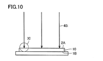
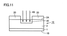
- the ion implantation angle formed by the implantation direction 40i see FIG. 10
- the variation in the surface of the main surface 2A is kept low. Therefore, referring to FIG.
- impurity implanted region 30 (p body region 13, n source) formed by implanting impurities from the opening of mask film 20 formed on main surface 2A of silicon carbide semiconductor substrate 10. Regions 14 and the like are formed in the same manner in the central portion and the outer peripheral portion of silicon carbide semiconductor substrate 10. From a different point of view, impurity implantation region 30 in silicon carbide semiconductor device 100 has a side wall portion extending in a direction perpendicular to main surface 2A.
- impurity implantation region 30 (p body region 13, n source region 14, etc.) is formed in silicon carbide semiconductor substrate 10 at the center and the outer periphery of silicon carbide semiconductor substrate 10. The position of the area and the way it expands are different.
- impurity implantation region 30 in silicon carbide semiconductor device 100 has a different main surface 2A in the direction in which the side wall portion extends locally with respect to main surface 2A.
- the impurity implantation region 30 having a side wall portion extending perpendicularly to the main surface 2A can be formed. Therefore, there is no problem that the shape of impurity implantation region 30 (for example, the direction in which the side wall extends) differs locally on main surface 2A, so that silicon carbide semiconductor device 100 can be obtained with high yield.
- the step of removing a part of back surface 1B is performed by chemically polishing back surface 1B, but is not limited thereto.
- the step (S30) of removing a part of the back surface 1B may be performed by, for example, reactive ion etching (RIE) of the back surface 1B.
- RIE reactive ion etching
- ICP-RIE Inductive Coupled Plasma-Reactive Ion Etching
- SF 6 or a mixed gas of SF 6 and O 2 as a reaction gas can be used.
- the step of removing a part of the back surface 1B may be performed, for example, by thermally etching the back surface 1B in a halogen gas atmosphere.
- a protective film may be formed on the main surface 2A.
- the protective film may be a thermal oxide film, for example.
- the halogen gas includes, for example, chlorine (Cl 2 ) gas.
- heating of silicon carbide semiconductor substrate 10 may be performed, for example, at about 700 ° C. or more and about 1000 ° C. or less.
- the step of removing a part of the back surface 1B may be performed, for example, by forming a thermal oxide film on the back surface 1B and then etching the thermal oxide film using hydrofluoric acid (HF). . Even in this way, the damage layer 3 can be removed.
- HF hydrofluoric acid
- the silicon carbide semiconductor device according to the present embodiment may have a field stop region (not shown) so as to surround guard ring region 5.
- the field stop region has n-type conductivity, and may be formed by high-temperature implantation in the impurity implantation step (S40) in the same manner as the source region 14 and the like. Since the silicon carbide semiconductor device according to the present embodiment is manufactured using flat silicon carbide semiconductor substrate 10 even under a high temperature environment, the arrangement and form of guard ring region 5 and field stop region are also principal surface 2A. The occurrence of problems such as local fluctuations can be suppressed. Specifically, for example, it is possible to suppress a change in the distance between the guard ring region 5 and the field stop region in the main surface 2A.
- the present invention is particularly advantageously applied to a large-diameter silicon carbide semiconductor substrate having an outer diameter of 100 mm or more, a method for manufacturing the same, and a method for manufacturing a silicon carbide semiconductor device using the silicon carbide semiconductor substrate.
Abstract
This silicon carbide semiconductor substrate comprises a base substrate (1) made from single crystal silicon carbide and having a principal surface area with an outer diameter of 100mm or more, and an epitaxial layer (2) formed on the principal surface (1A). The silicon carbide semiconductor substrate (10) has a warpage of -100μm to 100μm when the substrate temperature is at room temperature, and from -1.5mm to 1.5mm when the substrate temperature is 400°C.
Description
本発明は、炭化珪素半導体基板およびその製造方法、ならびに炭化珪素半導体装置の製造方法に関し、特に、高温に加熱処理されても平坦性の高い炭化珪素半導体基板およびその製造方法、ならびに炭化珪素半導体装置の製造方法に関する。
The present invention relates to a silicon carbide semiconductor substrate, a method for manufacturing the same, and a method for manufacturing a silicon carbide semiconductor device, and more particularly, a silicon carbide semiconductor substrate having high flatness even when heat-treated at a high temperature, a method for manufacturing the same, and a silicon carbide semiconductor device. It relates to the manufacturing method.
近年、半導体装置の製造に用いられる半導体基板として炭化珪素(SiC)結晶の利用が進められつつある。SiCは、より一般的に用いられているシリコン(Si)に比べて大きなバンドギャップを有する。そのため、SiCを用いた半導体装置は、耐圧が高く、オン抵抗が低く、また高温環境下での特性の低下が小さい、といった利点を有する。
In recent years, the use of silicon carbide (SiC) crystals is being promoted as a semiconductor substrate used in the manufacture of semiconductor devices. SiC has a larger band gap than silicon (Si), which is more commonly used. Therefore, a semiconductor device using SiC has advantages such as high withstand voltage, low on-resistance, and small deterioration in characteristics under a high temperature environment.
さらに、炭化珪素半導体装置を効率的に製造するために、炭化珪素半導体基板の大口径化が進められている。しかし、炭化珪素半導体基板の外径をたとえば6インチ程度とした場合には、炭化珪素半導体基板の平坦性が損なわれる。
Furthermore, in order to efficiently manufacture a silicon carbide semiconductor device, the silicon carbide semiconductor substrate is being increased in diameter. However, when the outer diameter of the silicon carbide semiconductor substrate is, for example, about 6 inches, the flatness of the silicon carbide semiconductor substrate is impaired.
特開2012-214376号公報には、直径が少なくとも約75ミリメートル(3インチ)であって、歪みが約5μm未満であり、反りが約5mm未満であり、TTVが約2.0μm未満であるSiCウエハが記載されている。具体的には、SiCブールを薄切りにしてウエハ状とし、薄切りにしたウエハを両面ラッパ上においてウエハを折り曲げるのに必要な下方力よりも小さい下方力を用いて、ラッピング・プロセスを開始することにより、歪み、反り及びTTVが低いウエハを生産することができることが記載されている。
JP 2012-214376 describes a SiC having a diameter of at least about 75 millimeters (3 inches), a strain of less than about 5 μm, a warp of less than about 5 mm, and a TTV of less than about 2.0 μm. A wafer is described. Specifically, by slicing the SiC boule into a wafer and starting the lapping process using a downward force that is less than the downward force required to fold the wafer on a double-sided wrapper. It is described that wafers with low distortion, warpage and TTV can be produced.
しかしながら、室温において炭化珪素半導体基板の反りおよびTTVが特開2012-214376号公報に記載されている範囲内にあっても、高温に加熱処理されることにより、平坦性が悪化する炭化珪素半導体基板が確認されている。たとえば、一般に炭化珪素半導体装置の製造方法におけるドーピングは、高温下においてイオン注入により行われるが、平坦性の悪い炭化珪素半導体基板は注入装置の静電チャックステージに吸着させることが困難であり、場合によっては基板が割れるなどの問題が生じることが確認されている。
However, even if the warpage and TTV of the silicon carbide semiconductor substrate are within the range described in JP 2012-214376 A at room temperature, the silicon carbide semiconductor substrate whose flatness deteriorates due to heat treatment at a high temperature Has been confirmed. For example, in general, doping in a method for manufacturing a silicon carbide semiconductor device is performed by ion implantation at a high temperature, but a silicon carbide semiconductor substrate having poor flatness is difficult to be adsorbed on the electrostatic chuck stage of the implantation device. It has been confirmed that problems such as breakage of the substrate may occur depending on the type.
また、平坦性の悪い炭化珪素半導体基板に対してイオン注入を行うと、イオンの注入方向に対して表面が垂直な領域と、イオンの注入方向に対して表面が垂直ではなく傾斜している領域とが生じることになる。この場合、炭化珪素半導体基板において形成される不純物領域の形状にはばらつき生じる。
In addition, when ion implantation is performed on a silicon carbide semiconductor substrate having poor flatness, a region where the surface is perpendicular to the ion implantation direction and a region where the surface is inclined rather than perpendicular to the ion implantation direction Will occur. In this case, the shape of the impurity region formed in the silicon carbide semiconductor substrate varies.
また、このような高温下における平坦性の悪化は、100mm以上の大口径の炭化珪素半導体基板において特に深刻な問題となっている。つまり、効率よく炭化珪素半導体装置を得るために大口径(特に100mm以上)の炭化珪素半導体基板を用いても、上述のような平坦性の悪化により炭化珪素半導体装置を歩留まり良く作製することは困難であった。
Further, such deterioration of flatness at high temperatures is a particularly serious problem in a silicon carbide semiconductor substrate having a large diameter of 100 mm or more. That is, even if a silicon carbide semiconductor substrate having a large diameter (especially 100 mm or more) is used in order to obtain a silicon carbide semiconductor device efficiently, it is difficult to manufacture the silicon carbide semiconductor device with a high yield due to the deterioration of the flatness as described above. Met.
本発明は上記のような課題を解決するためになされたものである。本発明の主たる目的は、高温下においても平坦性の高い炭化珪素半導体基板およびその製造方法、ならびに炭化珪素半導体装置の製造方法を提供することにある。また、大口径の炭化珪素半導体基板を用いて炭化珪素半導体装置を歩留まり良く作製することができる炭化珪素半導体装置の製造方法を提供することにある。
The present invention has been made to solve the above-described problems. A main object of the present invention is to provide a silicon carbide semiconductor substrate having high flatness even at high temperatures, a method for manufacturing the same, and a method for manufacturing a silicon carbide semiconductor device. Another object of the present invention is to provide a method for manufacturing a silicon carbide semiconductor device capable of manufacturing a silicon carbide semiconductor device with a high yield by using a large-diameter silicon carbide semiconductor substrate.
本発明に従った炭化珪素半導体基板10は、外径が100mm以上である主表面を有し、単結晶炭化珪素からなるベース基板1と、主面1A上に形成されたエピタキシャル層2とを備える。炭化珪素半導体基板10は、基板温度が室温であるときの反り量は-100μm以上100μm以下であり、基板温度が400℃であるときの反り量は-1.5mm以上1.5mm以下である。
Silicon carbide semiconductor substrate 10 according to the present invention has a main surface having an outer diameter of 100 mm or more, and includes a base substrate 1 made of single-crystal silicon carbide and an epitaxial layer 2 formed on main surface 1A. . Silicon carbide semiconductor substrate 10 has a warpage amount of −100 μm to 100 μm when the substrate temperature is room temperature, and a warp amount of −1.5 mm to 1.5 mm when the substrate temperature is 400 ° C.
本発明に従った炭化珪素半導体基板の製造方法は、外径が100mm以上である主表面を有し、単結晶炭化珪素からなるベース基板を準備する工程と、前記主表面上にエピタキシャル層を形成する工程と、前記ベース基板において前記主表面の反対側に位置する裏面の少なくとも一部を除去して、炭化珪素半導体基板を準備する工程と、前記炭化珪素半導体基板に不純物イオンを注入する工程とを備える。
A method of manufacturing a silicon carbide semiconductor substrate according to the present invention includes a step of preparing a base substrate having a main surface having an outer diameter of 100 mm or more and made of single crystal silicon carbide, and forming an epitaxial layer on the main surface A step of removing at least a part of the back surface of the base substrate opposite to the main surface to prepare a silicon carbide semiconductor substrate; and a step of implanting impurity ions into the silicon carbide semiconductor substrate; Is provided.
本発明によれば、高温下においても平坦性の高い炭化珪素半導体基板を得ることができる。また、炭化珪素半導体装置を歩留まり良く作製することができる炭化珪素半導体装置の製造方法を提供することができる。
According to the present invention, a silicon carbide semiconductor substrate having high flatness even at high temperatures can be obtained. In addition, it is possible to provide a method for manufacturing a silicon carbide semiconductor device capable of manufacturing a silicon carbide semiconductor device with a high yield.
[本願発明の実施形態の説明]
以下、図面を参照して、本発明の実施の形態について説明する。なお、以下の図面において、同一または相当する部分には同一の参照番号を付し、その説明は繰り返さない。また、本明細書中の結晶学的記載においては、個別方位を[]、集合方位を<>、個別面を()、集合面を{}でそれぞれ示している。また結晶学上の指数が負であることは、通常、”-”(バー)を数字の上に付すことによって表現されるが、本明細書中では数字の前に負の符号を付している。 [Description of Embodiment of Present Invention]
Embodiments of the present invention will be described below with reference to the drawings. In the following drawings, the same or corresponding parts are denoted by the same reference numerals, and the description thereof will not be repeated. In the crystallographic description in this specification, the individual orientation is indicated by [], the collective orientation is indicated by <>, the individual plane is indicated by (), and the collective plane is indicated by {}. In addition, a negative crystallographic index is usually expressed by adding “-” (bar) above a number. In this specification, a negative sign is added before the number. Yes.
はじめに、本発明の実施の形態の概要を列挙する。
(1)図1を参照して、本実施の形態に係る炭化珪素半導体基板10は、外径が100mm以上である主面2Aを有し、単結晶炭化珪素からなるベース基板1と、主面2A上に形成されたエピタキシャル層2とを備え、基板温度が室温であるときの反り量は-100μm以上100μm以下であり、基板温度が400℃であるときの反り量は-1.5mm以上1.5mm以下である。ここで、図2および図3を参照して、炭化珪素半導体基板10の「反り量」とは、炭化珪素半導体基板10を平面S1に載置したときの、炭化珪素半導体基板10の主面2Aにおいて平面S1に対して最も高い位置と最も低い位置との間の高さの差である。ここで、反り量の正負は、図2を参照して、炭化珪素半導体基板10の主面2Aが下に凸の場合(炭化珪素半導体基板10の中心位置が外周位置よりも平面S1に対して低く位置する場合)をマイナスとし、図3を参照して、上方に凸の場合(炭化珪素半導体基板10の中心位置が外周位置よりも平面S1に対して高く位置する場合)をプラスとする。また、「基板温度」とは、炭化珪素半導体基板10の主面2A側から放射温度計により測定される温度であり、たとえばイオン注入装置などの半導体製造装置において測定される。なお、本実施の形態に係る炭化珪素半導体基板10は、外径が100mm以上の大口径基板であって、好ましくは外径が125mm以上であり、より好ましくは外径が150mm以上である。 First, the outline of the embodiment of the present invention will be enumerated.
(1) Referring to FIG. 1, siliconcarbide semiconductor substrate 10 according to the present embodiment has a main surface 2A having an outer diameter of 100 mm or more, a base substrate 1 made of single-crystal silicon carbide, and a main surface 2A, the amount of warpage when the substrate temperature is room temperature is −100 μm or more and 100 μm or less, and the amount of warpage when the substrate temperature is 400 ° C. is −1.5 mm or more and 1 .5 mm or less. Here, referring to FIG. 2 and FIG. 3, “warping amount” of silicon carbide semiconductor substrate 10 means main surface 2 </ b> A of silicon carbide semiconductor substrate 10 when silicon carbide semiconductor substrate 10 is placed on plane S <b> 1. Is a difference in height between the highest position and the lowest position with respect to the plane S1. Here, referring to FIG. 2, the amount of warpage is positive or negative when main surface 2A of silicon carbide semiconductor substrate 10 is convex downward (the center position of silicon carbide semiconductor substrate 10 is relative to plane S1 relative to the outer peripheral position). Referring to FIG. 3, the case where it is convex upward (the case where the center position of silicon carbide semiconductor substrate 10 is located higher than plane S <b> 1 relative to the outer peripheral position) is positive. “Substrate temperature” is a temperature measured by a radiation thermometer from the main surface 2A side of silicon carbide semiconductor substrate 10, and is measured in a semiconductor manufacturing apparatus such as an ion implantation apparatus, for example. Silicon carbide semiconductor substrate 10 according to the present embodiment is a large-diameter substrate having an outer diameter of 100 mm or more, preferably has an outer diameter of 125 mm or more, and more preferably has an outer diameter of 150 mm or more.
(1)図1を参照して、本実施の形態に係る炭化珪素半導体基板10は、外径が100mm以上である主面2Aを有し、単結晶炭化珪素からなるベース基板1と、主面2A上に形成されたエピタキシャル層2とを備え、基板温度が室温であるときの反り量は-100μm以上100μm以下であり、基板温度が400℃であるときの反り量は-1.5mm以上1.5mm以下である。ここで、図2および図3を参照して、炭化珪素半導体基板10の「反り量」とは、炭化珪素半導体基板10を平面S1に載置したときの、炭化珪素半導体基板10の主面2Aにおいて平面S1に対して最も高い位置と最も低い位置との間の高さの差である。ここで、反り量の正負は、図2を参照して、炭化珪素半導体基板10の主面2Aが下に凸の場合(炭化珪素半導体基板10の中心位置が外周位置よりも平面S1に対して低く位置する場合)をマイナスとし、図3を参照して、上方に凸の場合(炭化珪素半導体基板10の中心位置が外周位置よりも平面S1に対して高く位置する場合)をプラスとする。また、「基板温度」とは、炭化珪素半導体基板10の主面2A側から放射温度計により測定される温度であり、たとえばイオン注入装置などの半導体製造装置において測定される。なお、本実施の形態に係る炭化珪素半導体基板10は、外径が100mm以上の大口径基板であって、好ましくは外径が125mm以上であり、より好ましくは外径が150mm以上である。 First, the outline of the embodiment of the present invention will be enumerated.
(1) Referring to FIG. 1, silicon
つまり、本実施の形態に係る炭化珪素半導体基板10は、外径が100mm以上と大口径基板であって、基板温度が400℃であるときの反り量が-1.5mm以上1.5mm以下と、高温下においても平坦性が高い。これにより、炭化珪素半導体基板10を用いて炭化珪素半導体装置の製造方法を実施する際に、当該製造プロセス中において炭化珪素半導体基板10に割れ等の異常が発生するリスクを低減することができる。具体的には、たとえば炭化珪素半導体装置の製造方法におけるドーピングが高温下での炭化珪素半導体基板10に対するイオン注入により行われる場合であって、炭化珪素半導体基板10をイオン注入装置の静電チャックステージで吸着する場合を考える。この場合、炭化珪素半導体基板10の高温(400℃)での反り量は十分に小さいため、炭化珪素半導体基板10には吸着によって大きな応力が加えられることない。そのため、炭化珪素半導体基板10に割れやクラックなどの異常が発生するリスクを低減することができる。
That is, silicon carbide semiconductor substrate 10 according to the present embodiment is a large-diameter substrate having an outer diameter of 100 mm or more, and a warpage amount when the substrate temperature is 400 ° C. is −1.5 mm or more and 1.5 mm or less. The flatness is high even at high temperatures. Thereby, when performing the manufacturing method of a silicon carbide semiconductor device using the silicon carbide semiconductor substrate 10, the risk that abnormality, such as a crack, may generate | occur | produce in the silicon carbide semiconductor substrate 10 during the said manufacturing process can be reduced. Specifically, for example, doping in the method for manufacturing a silicon carbide semiconductor device is performed by ion implantation into silicon carbide semiconductor substrate 10 at a high temperature, and silicon carbide semiconductor substrate 10 is used as an electrostatic chuck stage of the ion implantation device. Consider the case of adsorption with In this case, since the amount of warp of silicon carbide semiconductor substrate 10 at a high temperature (400 ° C.) is sufficiently small, large stress is not applied to silicon carbide semiconductor substrate 10 due to adsorption. Therefore, the risk of occurrence of abnormalities such as cracks and cracks in silicon carbide semiconductor substrate 10 can be reduced.
さらに、本実施の形態に係る炭化珪素半導体基板10は外径が100mm以上と大口径基板であって、高温下においても平坦性が高いため、炭化珪素半導体基板10を用いて炭化珪素半導体装置の製造プロセスを進捗させたときに炭化珪素半導体基板10上に特性バラつきの小さい炭化珪素半導体装置を作製することができる。具体的には、たとえば炭化珪素半導体基板10に対するイオン注入など、特定の方向から炭化珪素半導体基板10の主面2Aに対して加工を行う工程においても主面2Aの平坦性が高いため、主面2Aに対する被加工領域(注入領域)の配置や形態が主面2A内で局所的に変動するといった問題の発生を抑制できる。この結果、主面2A上における当該加工のバラつきを低減することができる。
Furthermore, silicon carbide semiconductor substrate 10 according to the present embodiment is a large-diameter substrate having an outer diameter of 100 mm or more, and has high flatness even at high temperatures. Therefore, silicon carbide semiconductor substrate 10 is used to form a silicon carbide semiconductor device. When the manufacturing process is advanced, a silicon carbide semiconductor device having a small variation in characteristics can be manufactured on silicon carbide semiconductor substrate 10. Specifically, since the flatness of main surface 2A is high even in a process of processing main surface 2A of silicon carbide semiconductor substrate 10 from a specific direction, such as ion implantation for silicon carbide semiconductor substrate 10, for example, the main surface Generation | occurrence | production of the problem that arrangement | positioning and form of the to-be-processed area | region (implantation area | region) with respect to 2A fluctuate locally within main surface 2A can be suppressed. As a result, variations in the processing on the main surface 2A can be reduced.
また、炭化珪素半導体基板10は、高精度の露光を行うために、たとえばLTV(Local Thickness Variation)が1μm以下であることが要求される。この場合、炭化珪素半導体基板の実際の厚み変動が1μm以下と小さくても、露光装置の真空チャックステージ上に吸着したときに炭化珪素半導体基板の反り量が大きいと、見かけ上のLTVが大きくなってしまう場合がある。これに対し、本実施の形態に係る炭化珪素半導体基板10は反り量が小さいため、見かけ上のLTVが大きくなることはなく、高精度の露光を行うことができる。以上より、大口径でかつ平坦性の高い炭化珪素半導体基板10を用いて炭化珪素半導体装置の製造プロセスを進捗させることにより、炭化珪素半導体装置を歩留まり良く作製することができる。
Further, silicon carbide semiconductor substrate 10 is required to have, for example, an LTV (Local Thickness Variation) of 1 μm or less in order to perform high-precision exposure. In this case, even if the actual thickness variation of the silicon carbide semiconductor substrate is as small as 1 μm or less, if the amount of warpage of the silicon carbide semiconductor substrate is large when adsorbed on the vacuum chuck stage of the exposure apparatus, the apparent LTV increases. May end up. On the other hand, since silicon carbide semiconductor substrate 10 according to the present embodiment has a small amount of warpage, the apparent LTV does not increase and high-precision exposure can be performed. As described above, the silicon carbide semiconductor device can be manufactured with high yield by advancing the manufacturing process of the silicon carbide semiconductor device using silicon carbide semiconductor substrate 10 having a large diameter and high flatness.
(2)本実施の形態に係る炭化珪素半導体基板10は、主面1A,2Aに垂直な方向におけるベース基板1の厚みが200μm以上700μm以下であってもよい。このようにしても、本実施の形態に係る炭化珪素半導体基板10は、基板温度が400℃であるときの反り量が-1.5mm以上1.5mm以下とすることができる。一般的に、炭化珪素基板において、ベース基板1の主面1A上に形成されるエピタキシャル層2の厚みは、数μm以上100μm以下程度である。そのため、ベース基板1の厚みが薄い場合には、炭化珪素半導体基板10の反り量は大きくなる。一方で、ベース基板1の厚みが厚い場合には、製造コストが高くなる。これに対して、本実施の形態に係る炭化珪素半導体基板10は、ベース基板1が700μmを超える程の厚みを有していなくても、高温下においても高い平坦性を有することができる。つまり、本実施の形態に係る炭化珪素基板の製造方法によれば、高温下においても高い平坦性を有する炭化珪素半導体基板10を低コストで得ることができる。
(2) In silicon carbide semiconductor substrate 10 according to the present embodiment, base substrate 1 in the direction perpendicular to main surfaces 1A and 2A may have a thickness of 200 μm or more and 700 μm or less. Even in this case, silicon carbide semiconductor substrate 10 according to the present embodiment can have a warpage amount of −1.5 mm or more and 1.5 mm or less when the substrate temperature is 400 ° C. Generally, in a silicon carbide substrate, the thickness of epitaxial layer 2 formed on main surface 1A of base substrate 1 is about several μm or more and 100 μm or less. Therefore, when base substrate 1 is thin, the amount of warpage of silicon carbide semiconductor substrate 10 increases. On the other hand, when the thickness of the base substrate 1 is thick, the manufacturing cost increases. In contrast, silicon carbide semiconductor substrate 10 according to the present embodiment can have high flatness even at a high temperature even if base substrate 1 does not have a thickness that exceeds 700 μm. That is, according to the method for manufacturing a silicon carbide substrate in accordance with the present embodiment, silicon carbide semiconductor substrate 10 having high flatness even at high temperatures can be obtained at low cost.
(3)本実施の形態に係る炭化珪素半導体基板10では、ベース基板1において、主面2Aの反対側に位置する裏面1Bの表面粗度は10nm以下であるのが好ましい。ベース基板1の裏面1Bの表面粗度が高い場合には、たとえば裏面1Bを構成する炭化珪素のうち珪素(Si)が高温環境下において過剰に抜けて、炭化した層(ダメージ層3)が形成されていることが考えられる。本発明者らは、ベース基板1の主面1A上にエピタキシャル層2を形成した後のベース基板1の裏面1Bの表面粗度を10nm以下とした炭化珪素半導体基板は、上述のように基板温度が400℃であるときの反り量が-1.5mm以上1.5mm以下であることを見出した。つまり、炭化珪素半導体基板10の基板温度を高温としたときに反り量が増大する原因の一つは、炭化珪素半導体基板10において、ベース基板1の裏面1Bに形成されたダメージ層3の残留歪みに起因した応力が生じるためであると推測される。
(3) In silicon carbide semiconductor substrate 10 according to the present embodiment, in base substrate 1, the surface roughness of back surface 1B located on the opposite side of main surface 2A is preferably 10 nm or less. When the surface roughness of the back surface 1B of the base substrate 1 is high, for example, silicon (Si) out of silicon carbide constituting the back surface 1B excessively escapes in a high temperature environment, and a carbonized layer (damage layer 3) is formed. It is thought that it is done. The inventors have described that a silicon carbide semiconductor substrate in which the surface roughness of the back surface 1B of the base substrate 1 after forming the epitaxial layer 2 on the main surface 1A of the base substrate 1 is 10 nm or less is the substrate temperature as described above. It was found that the amount of warping when the temperature was 400 ° C. was −1.5 mm or more and 1.5 mm or less. That is, one of the causes of the increase in the amount of warp when the substrate temperature of silicon carbide semiconductor substrate 10 is high is the residual strain of damaged layer 3 formed on back surface 1B of base substrate 1 in silicon carbide semiconductor substrate 10. It is presumed that this is due to the stress caused by.
(4)本実施の形態に係る炭化珪素半導体基板の製造方法は、外径が100mm以上である主面2Aを有し、単結晶炭化珪素からなるベース基板1を準備する工程(S10)と、主面2A上にエピタキシャル層2を形成する工程(S30)と、ベース基板1において主面2Aの反対側に位置する裏面1Bの少なくとも一部を除去する工程(S30)とを備えている。
(4) A method for manufacturing a silicon carbide semiconductor substrate according to the present embodiment includes a step (S10) of preparing base substrate 1 having a main surface 2A having an outer diameter of 100 mm or more and made of single-crystal silicon carbide; A step (S30) of forming the epitaxial layer 2 on the main surface 2A and a step (S30) of removing at least a part of the back surface 1B located on the opposite side of the main surface 2A in the base substrate 1 are provided.
つまり、本実施の形態に係る炭化珪素半導体基板の製造方法は、外径が100mm以上であり単結晶炭化珪素からなるベース基板1の主面1A上にエピタキシャル層2が形成された後に、ベース基板1の裏面1Bの一部が除去される。これにより、エピタキシャル層2を形成する工程(S20)においてベース基板1の裏面1Bにダメージ層3が生じても、ベース基板1の裏面1Bの一部を除去する工程(S30)においてダメージ層3は除去される。このようにして得られた炭化珪素半導体基板10は、外径が100mm以上であるとともに基板温度が室温であるときの反り量が-100μm以上100μm以下であり、基板温度が400℃であるときの反り量は-1.5mm以上1.5mm以下である。つまり、本実施の形態に係る炭化珪素半導体基板の製造方法によれば外径が100mm以上であっても高温環境下においても平坦性の高い炭化珪素半導体基板10を得ることができる。
That is, in the method for manufacturing the silicon carbide semiconductor substrate according to the present embodiment, after the epitaxial layer 2 is formed on main surface 1A of base substrate 1 having an outer diameter of 100 mm or more and made of single crystal silicon carbide, the base substrate Part of the back surface 1B of 1 is removed. Thereby, even if the damage layer 3 is formed on the back surface 1B of the base substrate 1 in the step (S20) of forming the epitaxial layer 2, the damage layer 3 is removed in the step (S30) of removing a part of the back surface 1B of the base substrate 1. Removed. Silicon carbide semiconductor substrate 10 thus obtained has an outer diameter of 100 mm or more, a warpage amount when the substrate temperature is room temperature, of −100 μm or more and 100 μm or less, and a substrate temperature of 400 ° C. The amount of warpage is not less than −1.5 mm and not more than 1.5 mm. That is, according to the method for manufacturing a silicon carbide semiconductor substrate in accordance with the present embodiment, silicon carbide semiconductor substrate 10 having high flatness can be obtained even in an environment of high temperature even if the outer diameter is 100 mm or more.
(5)本実施の形態に係る炭化珪素半導体基板の製造方法において、除去する工程(S30)は、裏面1Bを化学研磨(Chemical Mechanical Polishing:CMP)することにより行ってもよい。このようにしても、エピタキシャル層2を形成する工程(S20)においてベース基板1の裏面1Bにダメージ層3が生じても、ベース基板1の裏面1Bを化学研磨することによりダメージ層3を確実に除去することができる。
(5) In the method for manufacturing the silicon carbide semiconductor substrate according to the present embodiment, the removing step (S30) may be performed by chemically polishing the back surface 1B (Chemical Mechanical Polishing: CMP). Even if it does in this way, even if the damage layer 3 arises in the back surface 1B of the base substrate 1 in the process of forming the epitaxial layer 2 (S20), the damage layer 3 is reliably formed by chemically polishing the back surface 1B of the base substrate 1. Can be removed.
(6)本実施の形態に係る炭化珪素半導体基板の製造方法において、除去する工程(S30)は、裏面1Bを反応性イオンエッチングすることにより行ってもよい。このようにしても、エピタキシャル層2を形成する工程(S20)においてベース基板1の裏面1Bにダメージ層3が生じても、ベース基板1の裏面1Bを反応性イオンエッチングすることによりダメージ層3を確実に除去することができる。
(6) In the method for manufacturing the silicon carbide semiconductor substrate according to the present embodiment, the removing step (S30) may be performed by reactive ion etching of the back surface 1B. Even if it does in this way, even if the damage layer 3 arises in the back surface 1B of the base substrate 1 in the process (S20) of forming the epitaxial layer 2, the damage layer 3 is formed by reactive ion etching of the back surface 1B of the base substrate 1. It can be removed reliably.
(7)本実施の形態に係る炭化珪素半導体基板の製造方法において、除去する工程(S30)は、裏面1Bをハロゲンガス雰囲気下において熱エッチングすることにより行ってもよい。このようにしても、エピタキシャル層2を形成する工程(S20)においてベース基板1の裏面1Bにダメージ層3が生じても、ベース基板1の裏面1Bを熱エッチングすることによりダメージ層3を確実に除去することができる。
(7) In the method for manufacturing the silicon carbide semiconductor substrate according to the present embodiment, the removing step (S30) may be performed by thermally etching back surface 1B in a halogen gas atmosphere. Even if it does in this way, even if the damage layer 3 arises in the back surface 1B of the base substrate 1 in the process (S20) of forming the epitaxial layer 2, the damage layer 3 is reliably formed by thermally etching the back surface 1B of the base substrate 1. Can be removed.
(8)本実施の形態に係る炭化珪素半導体基板の製造方法において、除去する工程(S30)は、裏面1Bを熱酸化膜を形成した後、熱酸化膜をフッ化水素酸を用いてエッチングすることにより行ってもよい。このようにしても、エピタキシャル層2を形成する工程(S20)においてベース基板1の裏面1Bにダメージ層3が生じても、ベース基板1の裏面1Bに形成した熱酸化膜をフッ化水素酸を用いてエッチングすることによりダメージ層3を確実に除去することができる。
(8) In the method for manufacturing a silicon carbide semiconductor substrate according to the present embodiment, in the removing step (S30), after forming the thermal oxide film on back surface 1B, the thermal oxide film is etched using hydrofluoric acid. It may be done by. Even if it does in this way, even if the damage layer 3 arises in the back surface 1B of the base substrate 1 in the process (S20) of forming the epitaxial layer 2, the thermal oxide film formed on the back surface 1B of the base substrate 1 is made of hydrofluoric acid. The damage layer 3 can be reliably removed by using and etching.
(9)本実施の形態に係る炭化珪素半導体装置の製造方法は、外径が100mm以上である主面2Aを有し、単結晶炭化珪素からなるベース基板1を準備する工程(S10)と、主面2A上にエピタキシャル層2を形成する工程(S20)と、ベース基板1において主面2Aの反対側に位置する裏面1Bの少なくとも一部を除去して、炭化珪素半導体基板10を準備する工程(S30)と、炭化珪素半導体基板10に不純物イオンを注入する工程(S40)とを備える。
(9) A method for manufacturing a silicon carbide semiconductor device according to the present embodiment includes a step (S10) of preparing base substrate 1 having a main surface 2A having an outer diameter of 100 mm or more and made of single-crystal silicon carbide; A step of forming epitaxial layer 2 on main surface 2A (S20) and a step of preparing silicon carbide semiconductor substrate 10 by removing at least part of back surface 1B located on the opposite side of main surface 2A in base substrate 1 (S30) and a step of implanting impurity ions into silicon carbide semiconductor substrate 10 (S40).
つまり、本実施の形態に係る炭化珪素半導体装置の製造方法は、本実施の形態に係る炭化珪素半導体基板の製造方法により得られた炭化珪素半導体基板10を用い、炭化珪素半導体基板10上に炭化珪素半導体装置を製造する。上述のように、本実施の形態に係る炭化珪素半導体基板の製造方法により得られる炭化珪素半導体基板10は、外径が100mm以上であるとともに、基板温度が室温であるときの反り量が-100μm以上100μm以下であり、基板温度が400℃であるときの反り量は-1.5mm以上1.5mm以下である。つまり、炭化珪素半導体基板10に不純物イオンを注入する工程(S40)において、たとえば基板温度が400℃程度にまで加熱されたときにも、炭化珪素半導体基板10の反りを抑制して平坦性を維持することができる。そのため、工程(S40)において炭化珪素半導体基板10の主面2Aに対して不純物の注入方向のなす角度は、炭化珪素半導体基板10の外径が100mm以上であっても炭化珪素半導体基板10の主面2Aの面内位置によらず略一定とすることができる。その結果、主面2Aの面内位置によらずイオンの注入領域の形態(たとえば基板の深さ方向での注入領域の形状やイオンの濃度プロファイルなど)を略一定とすることができる。したがって、本実施の形態に係る炭化珪素半導体装置の製造方法によれば、炭化珪素半導体装置を歩留まり良く作製することができる。
That is, the method for manufacturing the silicon carbide semiconductor device according to the present embodiment uses silicon carbide semiconductor substrate 10 obtained by the method for manufacturing the silicon carbide semiconductor substrate according to the present embodiment, and carbonizes on silicon carbide semiconductor substrate 10. A silicon semiconductor device is manufactured. As described above, silicon carbide semiconductor substrate 10 obtained by the method for manufacturing a silicon carbide semiconductor substrate according to the present embodiment has an outer diameter of 100 mm or more and a warpage amount of −100 μm when the substrate temperature is room temperature. The amount of warpage when the substrate temperature is 100 μm or less and the substrate temperature is 400 ° C. is −1.5 mm to 1.5 mm. That is, in the step of implanting impurity ions into silicon carbide semiconductor substrate 10 (S40), for example, even when the substrate temperature is heated to about 400 ° C., warpage of silicon carbide semiconductor substrate 10 is suppressed and flatness is maintained. can do. Therefore, in the step (S40), the angle formed by the impurity implantation direction with respect to main surface 2A of silicon carbide semiconductor substrate 10 is the main surface of silicon carbide semiconductor substrate 10 even if the outer diameter of silicon carbide semiconductor substrate 10 is 100 mm or more. It can be made substantially constant regardless of the in-plane position of the surface 2A. As a result, the form of the ion implantation region (for example, the shape of the implantation region in the depth direction of the substrate and the ion concentration profile) can be made substantially constant regardless of the in-plane position of the main surface 2A. Therefore, according to the method for manufacturing the silicon carbide semiconductor device according to the present embodiment, the silicon carbide semiconductor device can be manufactured with a high yield.
[本願発明の実施形態の詳細]
次に、本発明の実施の形態の詳細について説明する。 [Details of the embodiment of the present invention]
Next, details of the embodiment of the present invention will be described.
次に、本発明の実施の形態の詳細について説明する。 [Details of the embodiment of the present invention]
Next, details of the embodiment of the present invention will be described.
(実施の形態1)
図1を参照して、実施の形態1に係る炭化珪素半導体基板10について説明する。本実施の形態に係る炭化珪素半導体基板10は、ベース基板1と、ベース基板1の主面1A上に形成されたエピタキシャル層2とを備える。 (Embodiment 1)
With reference to FIG. 1, siliconcarbide semiconductor substrate 10 according to the first embodiment will be described. Silicon carbide semiconductor substrate 10 according to the present embodiment includes a base substrate 1 and an epitaxial layer 2 formed on main surface 1 </ b> A of base substrate 1.
図1を参照して、実施の形態1に係る炭化珪素半導体基板10について説明する。本実施の形態に係る炭化珪素半導体基板10は、ベース基板1と、ベース基板1の主面1A上に形成されたエピタキシャル層2とを備える。 (Embodiment 1)
With reference to FIG. 1, silicon
ベース基板1は、単結晶炭化珪素からなり、外径が6インチである主面1Aを有している。ベース基板1を構成する炭化珪素は、たとえば六方晶の結晶構造を有しており、好ましくは結晶多形(ポリタイプ)が4H-SiCである。ベース基板1は、たとえば窒素(N)などのn型不純物を高濃度で含んでおり、導電型はn型である。ベース基板1の不純物濃度は、たとえば1.0×1018cm-3以上1.0×1018cm-3以下程度である。主面1Aは、たとえば{0001}面であってもよいし、{0001}面に対するオフ角が1°以上10°以下である面であってもよい。ベース基板1の厚みは、たとえば200μm以上700μm以下程度であり、好ましくは300μm以上600μm以下である。炭化珪素半導体基板10において、ベース基板1の主面1Aの反対側に位置する裏面1Bには、炭素と珪素炭化珪素をダメージ層3(図6参照)が形成されていない。なお、ダメージ層3については後述する。
Base substrate 1 is made of single crystal silicon carbide and has a main surface 1A having an outer diameter of 6 inches. Silicon carbide constituting base substrate 1 has, for example, a hexagonal crystal structure, and preferably has a crystal polymorph (polytype) of 4H—SiC. Base substrate 1 contains an n-type impurity such as nitrogen (N) at a high concentration, and the conductivity type is n-type. The impurity concentration of the base substrate 1 is, for example, about 1.0 × 10 18 cm −3 or more and 1.0 × 10 18 cm −3 or less. Main surface 1A may be, for example, a {0001} plane or a plane having an off angle of 1 ° or more and 10 ° or less with respect to the {0001} plane. The thickness of the base substrate 1 is, for example, about 200 μm to 700 μm, preferably 300 μm to 600 μm. In silicon carbide semiconductor substrate 10, damage layer 3 (see FIG. 6) of carbon and silicon silicon carbide is not formed on back surface 1B located on the opposite side of main surface 1A of base substrate 1. The damage layer 3 will be described later.
エピタキシャル層2は、ベース基板1の主面1A上にエピタキシャル成長により形成された炭化珪素からなる層である。エピタキシャル層2は、たとえば窒素(N)などのn型不純物を含んでおり、エピタキシャル層2の導電型はn型である。エピタキシャル層2の不純物濃度は、ベース基板1の不純物濃度よりも低くてもよい。エピタキシャル層2の不純物濃度は、たとえば7.5×1015cm-2程度である。エピタキシャル層2の膜厚は、たとえば5μm以上40μm以下程度である。
Epitaxial layer 2 is a layer made of silicon carbide formed by epitaxial growth on main surface 1 </ b> A of base substrate 1. Epitaxial layer 2 contains an n-type impurity such as nitrogen (N), for example, and the conductivity type of epitaxial layer 2 is n-type. The impurity concentration of the epitaxial layer 2 may be lower than the impurity concentration of the base substrate 1. The impurity concentration of the epitaxial layer 2 is, for example, about 7.5 × 10 15 cm −2 . The film thickness of the epitaxial layer 2 is, for example, about 5 μm to 40 μm.
炭化珪素半導体基板10は、基板温度が室温であるときの反り量は-100μm以上100μm以下であり、好ましくは40μm以上40μm以下である。また、炭化珪素半導体基板10は、基板温度が100℃以上500℃以下であるときの反り量が-1.5mm以上1.5mm以下であり、好ましくは-1.0mm以上1.0mm以下である。より好ましくは、基板温度が200℃以上400℃以下であるときの反り量が-1.5mm以上1.5mm以下であり、さらに好ましくは-1.0mm以上1.0mm以下である。
The silicon carbide semiconductor substrate 10 has a warpage amount of −100 μm or more and 100 μm or less, preferably 40 μm or more and 40 μm or less when the substrate temperature is room temperature. Further, silicon carbide semiconductor substrate 10 has a warpage amount of −1.5 mm to 1.5 mm, preferably −1.0 mm to 1.0 mm when the substrate temperature is 100 ° C. to 500 ° C. . More preferably, the amount of warpage when the substrate temperature is 200 ° C. or more and 400 ° C. or less is −1.5 mm or more and 1.5 mm or less, and more preferably −1.0 mm or more and 1.0 mm or less.
次に、図4~図7を参照して、本実施の形態に係る炭化珪素半導体基板の製造方法について説明する。
Next, a method for manufacturing the silicon carbide semiconductor substrate according to the present embodiment will be described with reference to FIGS.
図4および図5を参照して、まず、外径が6インチである主面1Aを有し、単結晶炭化珪素からなるベース基板1が準備される(工程(S10))。外径が6インチであるベース基板1は任意の方法で準備される。なお、ベース基板1の外径は100mm以上(たとえば5インチや8インチなど)であってもよい。
4 and 5, first, base substrate 1 having a main surface 1A having an outer diameter of 6 inches and made of single crystal silicon carbide is prepared (step (S10)). The base substrate 1 having an outer diameter of 6 inches is prepared by an arbitrary method. The outer diameter of the base substrate 1 may be 100 mm or more (for example, 5 inches or 8 inches).
図6を参照して、次に、ベース基板1の主面1A上にエピタキシャル成長法により、エピタキシャル層2が形成される(工程(S20))。エピタキシャル成長はCVD法により行われる。原料ガスとしては、たとえば、シラン(SiH4)とプロパン(C3H8)との混合ガスを用い得る。この際、不純物として、たとえば窒素(N)やリン(P)を導入してもよい。
Referring to FIG. 6, next, epitaxial layer 2 is formed on main surface 1A of base substrate 1 by an epitaxial growth method (step (S20)). Epitaxial growth is performed by a CVD method. As the source gas, for example, a mixed gas of silane (SiH 4 ) and propane (C 3 H 8 ) can be used. At this time, for example, nitrogen (N) or phosphorus (P) may be introduced as impurities.
本工程(S20)を実施した後の時点で、ベース基板1の裏面1Bの全面または一部において、珪素(Si)原子が抜けることにより炭素(C)原子の濃度が相対的に高くなったダメージ層3(炭化層)が形成されることがある。ダメージ層3は、たとえば0.001μm以上10μm以下程度の厚みで形成されることがあり、1μm以上の厚みで形成された場合には裏面1Bにおける白濁として目視で確認できることがある。ダメージ層3が形成されている領域の裏面1Bの表面粗さ(Ra)は0.001μm以上である。本工程(S20)を実施した後の時点で、裏面1Bにダメージ層3が形成されているベース基板1とエピタキシャル層2との積層体4は、基板温度が室温であるときの反りが、たとえば-150μm以上150μm以下である。
Damage at which the concentration of carbon (C) atoms is relatively high due to the escape of silicon (Si) atoms in the whole or part of the back surface 1B of the base substrate 1 at the time after performing this step (S20). Layer 3 (carbonized layer) may be formed. The damaged layer 3 may be formed with a thickness of about 0.001 μm or more and 10 μm or less, for example, and when formed with a thickness of 1 μm or more, it may be visually confirmed as white turbidity on the back surface 1B. The surface roughness (Ra) of the back surface 1B of the region where the damage layer 3 is formed is 0.001 μm or more. At the time after performing this step (S20), the laminate 4 of the base substrate 1 and the epitaxial layer 2 on which the damaged layer 3 is formed on the back surface 1B has warpage when the substrate temperature is room temperature, for example, -150 μm or more and 150 μm or less.
図7を参照して、次に、ベース基板1の裏面1Bの少なくとも一部が除去される(工程(S30))。具体的には、積層体4におけるベース基板1の裏面1BはCMP研磨されることによりダメージ層3が除去される。ベース基板1の裏面1Bの研磨量は、たとえば0.001μm以上10μm以下である。本工程(S30)の研磨後における裏面1Bの表面粗さ(Ra)は、10nm以下であり、好ましくは1nm以下である。
Referring to FIG. 7, next, at least a part of back surface 1B of base substrate 1 is removed (step (S30)). Specifically, the damage layer 3 is removed by CMP polishing of the back surface 1B of the base substrate 1 in the laminate 4. The polishing amount of the back surface 1B of the base substrate 1 is, for example, not less than 0.001 μm and not more than 10 μm. The surface roughness (Ra) of the back surface 1B after the polishing in this step (S30) is 10 nm or less, preferably 1 nm or less.
次に、本実施の形態に係る炭化珪素半導体基板10およびその製造方法の作用効果について説明する。本実施の形態に係る炭化珪素半導体基板10は、外径が6インチであるベース基板1とベース基板1の主面1A上に形成されたエピタキシャル層2とが積層してなる積層体4の裏面1B上から、ダメージ層3が除去された構成を備えている。これにより、炭化珪素半導体基板10は、基板温度が室温であるときの反りが-100μm以上100μm以下であるとともに、基板温度が100℃以上500℃以下であるときの反り量が-1.5mm以上1.5mm以下とすることができる。さらに、炭化珪素半導体基板10は、基板温度が室温であるときの反りが-100μm以上100μm以下であるとともに、基板温度が200℃以上400℃以下であるときの反り量が-1.5mm以上1.5mm以下とすることもできる。また、本実施の形態においては、基板温度を100℃以上500℃以下としたときに上記の反り量の範囲内に抑えることができるか否か、つまりダメージ層3を充分に除去し得たかは裏面1Bの表面粗さで確認することができる。具体的には、表面粗さ(Ra)を10nm以下とすることで、上述のように高温時においても反り量の小さい炭化珪素半導体基板10を得ることができる。さらに、表面粗さ(Ra)を1nm以下となるように裏面1Bを研磨すれば、ダメージ層3を十分に除去することができる。その結果、本実施の形態に係る炭化珪素半導体基板の製造方法によれば、基板温度が100℃以上500℃以下程度になるまで加熱された場合にも反り量が-1.0mm以上1.0mm以下と十分に小さい炭化珪素半導体基板10を得ることができる。また、本実施の形態に係る炭化珪素半導体基板の製造方法によれば、基板温度が200℃以上400℃以下程度になるまで加熱された場合にも反り量が-1.0mm以上1.0mm以下と十分に小さい炭化珪素半導体基板10を得ることもできる。
Next, functions and effects of silicon carbide semiconductor substrate 10 and the method for manufacturing the same according to the present embodiment will be described. Silicon carbide semiconductor substrate 10 according to the present embodiment has a back surface of laminate 4 in which base substrate 1 having an outer diameter of 6 inches and epitaxial layer 2 formed on main surface 1A of base substrate 1 are laminated. The damage layer 3 is removed from 1B. Thus, silicon carbide semiconductor substrate 10 has a warp of −100 μm or more and 100 μm or less when the substrate temperature is room temperature, and a warp amount of −1.5 mm or more when the substrate temperature is 100 ° C. or more and 500 ° C. or less. It can be 1.5 mm or less. Further, silicon carbide semiconductor substrate 10 has a warp of −100 μm or more and 100 μm or less when the substrate temperature is room temperature, and a warp amount of −1.5 mm or more and 1 or less when the substrate temperature is 200 ° C. or more and 400 ° C. or less. .5 mm or less. Further, in the present embodiment, whether the substrate layer temperature is 100 ° C. or more and 500 ° C. or less can be suppressed within the range of the warp amount, that is, whether the damaged layer 3 has been sufficiently removed. It can be confirmed by the surface roughness of the back surface 1B. Specifically, by setting the surface roughness (Ra) to 10 nm or less, silicon carbide semiconductor substrate 10 having a small amount of warpage can be obtained even at a high temperature as described above. Furthermore, if the back surface 1B is polished so that the surface roughness (Ra) is 1 nm or less, the damaged layer 3 can be sufficiently removed. As a result, according to the method for manufacturing a silicon carbide semiconductor substrate according to the present embodiment, even when the substrate temperature is heated to about 100 ° C. or higher and about 500 ° C. or lower, the amount of warpage is −1.0 mm to 1.0 mm. Silicon carbide semiconductor substrate 10 which is sufficiently small as follows can be obtained. In addition, according to the method for manufacturing a silicon carbide semiconductor substrate in accordance with the present embodiment, the amount of warpage is −1.0 mm or more and 1.0 mm or less even when the substrate temperature is heated to about 200 ° C. or more and 400 ° C. or less. A sufficiently small silicon carbide semiconductor substrate 10 can also be obtained.
また、本実施の形態に係る炭化珪素半導体基板の製造方法により作製される炭化珪素半導体基板10は、ベース基板1の外径が6インチであって、ベース基板1の厚みが200μm以上700μm以下のときにも、基板温度が100℃以上500℃以下程度にまで加熱された場合にも、反り量が小さく高い平坦性を有することができる。言い換えると、本実施の形態に係る炭化珪素半導体基板10は、ベース基板1が700μmを超える程の厚みを有していなくても、高温下においても高い平坦性を有することができる。その結果、本実施の形態に係る炭化珪素半導体基板の製造方法によれば、高温下においても高い平坦性を有する大口径の炭化珪素半導体基板10を、低コストで得ることができる。
Silicon carbide semiconductor substrate 10 manufactured by the method for manufacturing a silicon carbide semiconductor substrate according to the present embodiment has an outer diameter of base substrate 1 of 6 inches and a thickness of base substrate 1 of 200 μm or more and 700 μm or less. Sometimes, even when the substrate temperature is heated to about 100 ° C. or more and about 500 ° C. or less, the amount of warpage is small and high flatness can be obtained. In other words, silicon carbide semiconductor substrate 10 according to the present embodiment can have high flatness even at a high temperature even if base substrate 1 does not have a thickness exceeding 700 μm. As a result, according to the method for manufacturing the silicon carbide semiconductor substrate according to the present embodiment, silicon carbide semiconductor substrate 10 having a large diameter and having high flatness even at high temperatures can be obtained at low cost.
図8を参照して、次に、本実施の形態に係る炭化珪素半導体装置について説明する。本実施の形態に係る炭化珪素半導体装置は、素子領域IR(活性領域)と、素子領域IRを取り囲む終端領域OR(無効領域)とを有する。終端領域ORはガードリング領域5を含む。つまり、素子領域IRはガードリング領域5に取り囲まれている。素子領域IRにはトランジスタやダイオードなどの半導体素子7が設けられている。
Next, with reference to FIG. 8, a silicon carbide semiconductor device according to the present embodiment will be described. The silicon carbide semiconductor device according to the present embodiment has an element region IR (active region) and a termination region OR (invalid region) surrounding element region IR. Termination region OR includes guard ring region 5. That is, the element region IR is surrounded by the guard ring region 5. A semiconductor element 7 such as a transistor or a diode is provided in the element region IR.
半導体素子7は、たとえば六方晶炭化珪素からなる炭化珪素半導体基板10と、ゲート絶縁膜15と、ゲート電極17と、ソース電極16と、ドレイン電極19とを主に備える。炭化珪素半導体基板10は、ベース基板1とエピタキシャル層2とを備え、エピタキシャル層2は、ドリフト領域12と、pボディ領域13と、n+ソース領域14と、p+領域18とを主に有する。
The semiconductor element 7 mainly includes, for example, a silicon carbide semiconductor substrate 10 made of hexagonal silicon carbide, a gate insulating film 15, a gate electrode 17, a source electrode 16, and a drain electrode 19. Silicon carbide semiconductor substrate 10 includes a base substrate 1 and an epitaxial layer 2, and epitaxial layer 2 mainly includes a drift region 12, a p body region 13, an n + source region 14, and a p + region 18. .
ドリフト領域12は、エピタキシャル層2であって、pボディ領域13、n+ソース領域14、およびp+領域18が形成されていない領域である。
The drift region 12 is the epitaxial layer 2 where the p body region 13, the n + source region 14, and the p + region 18 are not formed.
pボディ領域13はp型の導電型を有する。pボディ領域13は、ドリフト領域12において、炭化珪素半導体基板10の主面2Aを含んで形成されている。pボディ領域13に含まれるp型不純物は、たとえばアルミニウム(Al)、ホウ素(B)などである。pボディ領域13に含まれるアルミニウムなどの不純物濃度はたとえば1×1017cm-3程度である。
P body region 13 has p type conductivity. P body region 13 is formed in drift region 12 including main surface 2 </ b> A of silicon carbide semiconductor substrate 10. The p-type impurity contained in p body region 13 is, for example, aluminum (Al), boron (B), or the like. The impurity concentration of aluminum or the like contained in p body region 13 is, for example, about 1 × 10 17 cm −3 .
n+ソース領域14はn型の導電型を有する。n+ソース領域14は、主面2Aを含み、かつpボディ領域13に取り囲まれるように、pボディ領域13の内部に形成されている。n+ソース領域14に含まれるn型不純物は、たとえばP(リン)などである。n+ソース領域14に含まれるリンなどの不純物濃度は、ドリフト領域12に含まれるn型不純物よりも高い濃度であり、たとえば1×1020cm-3程度である。
N + source region 14 has n type conductivity. N + source region 14 is formed inside p body region 13 so as to include main surface 2 A and be surrounded by p body region 13. The n-type impurity contained in the n + source region 14 is, for example, P (phosphorus). The concentration of impurities such as phosphorus contained in n + source region 14 is higher than that of n-type impurities contained in drift region 12, for example, about 1 × 10 20 cm −3 .
p+領域18はp型の導電型を有する。p+領域18は、主面2Aおよびpボディ領域13と接し、n+ソース領域14の中央付近を貫通するように形成されている。p+領域18は、p型不純物、たとえばAl、Bなどをpボディ領域13に含まれるp型不純物よりも高い濃度、たとえば1×1020cm-3程度の濃度で含んでいる。
The p + region 18 has p type conductivity. P + region 18 is formed so as to contact main surface 2A and p body region 13 and penetrate the vicinity of the center of n + source region 14. The p + region 18 contains p-type impurities such as Al and B at a higher concentration than the p-type impurities contained in the p body region 13, for example, about 1 × 10 20 cm −3 .
ゲート絶縁膜15は、一方のn+ソース領域14の上部表面から他方のn+ソース領域14の上部表面にまで延在するようにドリフト領域12に接して形成されている。ゲート絶縁膜15はたとえば二酸化珪素(SiO2)からなっている。
Gate insulating film 15 is formed in contact with drift region 12 so as to extend from the upper surface of one n + source region 14 to the upper surface of the other n + source region 14. The gate insulating film 15 is made of, for example, silicon dioxide (SiO 2 ).
ゲート電極17は、一方のn+ソース領域14上から他方のn+ソース領域14上にまで延在するように、ゲート絶縁膜15上に接触して配置されている。ゲート電極17は、たとえばポリシリコン、Alなどの導電体からなっている。
The gate electrode 17 is disposed in contact with the gate insulating film 15 so as to extend from one n + source region 14 to the other n + source region 14. The gate electrode 17 is made of a conductor such as polysilicon or Al.
ソース電極16は、主面2Aにおいてn+ソース領域14およびp+領域18と接触して配置されている。ソース電極16は、たとえばチタン(Ti)原子、Al原子およびシリコン(Si)原子を含んでいる。これにより、ソース電極16はn型炭化珪素領域(n+ソース領域14)およびp型炭化珪素領域(p+領域18)のいずれに対してもオーミック接触することができる。
The source electrode 16 is disposed in contact with the n + source region 14 and the p + region 18 on the main surface 2A. Source electrode 16 includes, for example, titanium (Ti) atoms, Al atoms, and silicon (Si) atoms. Thereby, source electrode 16 can make ohmic contact with both n-type silicon carbide region (n + source region 14) and p-type silicon carbide region (p + region 18).
ドレイン電極19は、炭化珪素半導体基板10において裏面1Bに接触して形成されている。このドレイン電極19は、たとえば上記ソース電極16と同様の構成を有していてもよいし、ニッケル(Ni)など、炭化珪素半導体基板10(ベース基板1)とオーミック接触可能な他の材料からなっていてもよい。これにより、ドレイン電極19はベース基板1と電気的に接続されている。
The drain electrode 19 is formed in contact with the back surface 1B in the silicon carbide semiconductor substrate 10. The drain electrode 19 may have the same configuration as the source electrode 16, for example, and is made of another material capable of ohmic contact with the silicon carbide semiconductor substrate 10 (base substrate 1) such as nickel (Ni). It may be. Thereby, the drain electrode 19 is electrically connected to the base substrate 1.
ガードリング領域5は、平面形状が環状であり、半導体素子7が設けられた素子領域IRを取り囲むように、炭化珪素半導体基板10の終端領域ORに配置されている。ガードリング領域5はp型(第2導電型)を有する。ガードリング領域5はガードリングとして作用する導電領域である。
The guard ring region 5 has an annular planar shape, and is disposed in the termination region OR of the silicon carbide semiconductor substrate 10 so as to surround the element region IR provided with the semiconductor element 7. Guard ring region 5 has p-type (second conductivity type). The guard ring region 5 is a conductive region that acts as a guard ring.
ガードリング領域5の複数のガードリング6には、たとえばホウ素やアルミニウムなどの不純物が含まれている。複数のガードリング6の各々における不純物濃度はpボディ領域13の不純物濃度よりも低い。複数のガードリング6の各々における当該不純物の濃度はたとえば1.3×1013cm-3であり、好ましくは8×1012cm-3以上1.4×1013cm-3以下程度である。
The plurality of guard rings 6 in the guard ring region 5 contain impurities such as boron and aluminum. The impurity concentration in each of the plurality of guard rings 6 is lower than the impurity concentration in p body region 13. The concentration of the impurity in each of the plurality of guard rings 6 is, for example, 1.3 × 10 13 cm −3 , and preferably about 8 × 10 12 cm −3 to 1.4 × 10 13 cm −3 .
図9を参照して、次に、本実施の形態に係る炭化珪素半導体装置の製造方法について説明する。本実施の形態に係る炭化珪素半導体装置の製造方法は、本実施の形態に係る炭化珪素半導体基板を用いて作製される。
Referring to FIG. 9, next, a method for manufacturing the silicon carbide semiconductor device according to the present embodiment will be described. The method for manufacturing the silicon carbide semiconductor device according to the present embodiment is manufactured using the silicon carbide semiconductor substrate according to the present embodiment.
まず、上述のようにして得られた炭化珪素半導体基板10を準備する(工程(S10)~工程(S30))。図9を参照して、次に、炭化珪素半導体基板10の主面2Aに対して不純物を注入することにより、エピタキシャル層2に、pボディ領域13、nソース領域14、p+領域18、およびガードリング領域5を形成する(工程(S40))。具体的には、導電型がn型のエピタキシャル層2に、p型不純物としてたとえばAlがイオン注入されることにより、導電型がp型のpボディ領域13が形成される。さらに、pボディ領域13に、n型不純物としてたとえばPがイオン注入されることにより、導電型がn型のnソース領域14が形成される。さらに、p型不純物としてたとえばAlがイオン注入されることにより、導電型がp型のp+領域18が形成される。さらに、p型不純物としてたとえばAlがイオン注入されることにより、導電型がp型のガードリング領域5が形成される。このとき、本工程(S40)におけるイオン注入は、たとえば炭化珪素半導体基板10の基板温度を100℃以上500℃以下程度に昇温させた状態で行われる(いわゆる、高温注入)。本工程(S40)を実施前および実施した後の時点において、炭化珪素半導体基板10の反り量は-1.5mm以上1.5mm以下である。また、上述のように、本実施の形態に係る炭化珪素半導体基板の製造方法において、たとえば裏面1Bを表面粗さ(Ra)を1nm以下となるように研磨することによってダメージ層3を十分に除去しておけば、本工程(S40)を実施前および実施した後の時点において、炭化珪素半導体基板10の反り量は-1.0mm以上1.0mm以下とすることができる。
First, silicon carbide semiconductor substrate 10 obtained as described above is prepared (step (S10) to step (S30)). Referring to FIG. 9, next, impurities are implanted into main surface 2 </ b> A of silicon carbide semiconductor substrate 10, so that p body region 13, n source region 14, p + region 18, and guard are formed in epitaxial layer 2. The ring region 5 is formed (step (S40)). Specifically, for example, Al is ion-implanted as a p-type impurity into epitaxial layer 2 having a conductivity type of n to form p body region 13 having a conductivity type of p type. Further, for example, P is ion-implanted as an n-type impurity in p body region 13, thereby forming n source region 14 having an n conductivity type. Further, for example, Al is ion-implanted as a p-type impurity, whereby p + region 18 having a p-type conductivity is formed. Furthermore, for example, Al is ion-implanted as a p-type impurity, whereby a p-type guard ring region 5 is formed. At this time, ion implantation in this step (S40) is performed, for example, in a state where the substrate temperature of silicon carbide semiconductor substrate 10 is raised to about 100 ° C. or higher and about 500 ° C. or lower (so-called high temperature implantation). Before and after performing this step (S40), warpage of silicon carbide semiconductor substrate 10 is not less than −1.5 mm and not more than 1.5 mm. Further, as described above, in the method for manufacturing the silicon carbide semiconductor substrate according to the present embodiment, damaged layer 3 is sufficiently removed by polishing back surface 1B so that the surface roughness (Ra) is 1 nm or less, for example. In this case, the warpage amount of silicon carbide semiconductor substrate 10 can be set to −1.0 mm or more and 1.0 mm or less before and after the present step (S40).
次に、イオン注入により添加された不純物を活性化するための熱処理が行われる(工程(S50))。熱処理の温度は、好ましくは1500℃以上1900℃以下であり、たとえば1700℃程度である。熱処理の時間は、たとえば30分程度である。熱処理の雰囲気は、好ましくは不活性ガス雰囲気であり、たとえばアルゴン(Ar)雰囲気である。本工程(S50)を実施した後の時点において、炭化珪素半導体基板10の反り量は-1.5mm以上1.5mm以下である。また、上述のように、本実施の形態に係る炭化珪素半導体基板の製造方法において、たとえば裏面1Bを表面粗さ(Ra)を1nm以下となるように研磨することによってダメージ層3を十分に除去しておけば、本工程(S50)を実施前および実施した後の時点において、炭化珪素半導体基板10の反り量は-1.0mm以上1.0mm以下とすることができる。
Next, heat treatment for activating the impurities added by ion implantation is performed (step (S50)). The temperature of the heat treatment is preferably 1500 ° C. or higher and 1900 ° C. or lower, for example, about 1700 ° C. The heat treatment time is, for example, about 30 minutes. The atmosphere of the heat treatment is preferably an inert gas atmosphere, for example, an argon (Ar) atmosphere. At the time after performing this step (S50), the warpage amount of silicon carbide semiconductor substrate 10 is not less than −1.5 mm and not more than 1.5 mm. Further, as described above, in the method for manufacturing the silicon carbide semiconductor substrate according to the present embodiment, damaged layer 3 is sufficiently removed by polishing back surface 1B so that the surface roughness (Ra) is 1 nm or less, for example. In this case, the warpage amount of silicon carbide semiconductor substrate 10 can be set to −1.0 mm or more and 1.0 mm or less before and after performing this step (S50).
次に、ゲート絶縁膜15が形成される(工程(S60))。具体的には、まず、所望の不純物領域が形成された炭化珪素半導体基板10が熱酸化される。熱酸化は、たとえば酸素雰囲気中で1300℃程度に加熱し、40分間程度保持することにより実施することができる。これにより、炭化珪素半導体基板10の主面2A上にSiO2からなるゲート絶縁膜15が形成される。
Next, the gate insulating film 15 is formed (step (S60)). Specifically, first, silicon carbide semiconductor substrate 10 on which a desired impurity region is formed is thermally oxidized. Thermal oxidation can be carried out, for example, by heating to about 1300 ° C. in an oxygen atmosphere and holding for about 40 minutes. Thereby, gate insulating film 15 made of SiO 2 is formed on main surface 2A of silicon carbide semiconductor substrate 10.
次に、ゲート電極17が形成される(工程(S70))。この工程では、たとえば導電体であるポリシリコン、Alなどからなるゲート電極17が、一方のn+ソース領域14上から他方のn+ソース領域14上にまで延在するとともに、ゲート絶縁膜15に接触するように形成される。ゲート電極17の材料としてポリシリコンを採用する場合、当該ポリシリコンは、Pが1×1020cm-3を超える高い濃度で含まれるものとすることができる。その後、ゲート電極17を覆うように、たとえばSiO2からなる絶縁膜が形成される。
Next, the gate electrode 17 is formed (step (S70)). In this step, for example, a gate electrode 17 made of polysilicon, Al, or the like, which is a conductor, extends from one n + source region 14 to the other n + source region 14 and is formed on the gate insulating film 15. Formed to contact. When polysilicon is adopted as the material of the gate electrode 17, the polysilicon can be contained at a high concentration of P exceeding 1 × 10 20 cm −3 . Thereafter, an insulating film made of, for example, SiO 2 is formed so as to cover gate electrode 17.
次に、オーミック電極が形成される(工程(S80))。具体的には、たとえばp+領域18およびn+ソース領域14の一部が露出するような開口部を有するレジストパターンを形成し、たとえばSi原子、Ti原子、およびAl原子とを含有する金属膜が基板全面に形成される。オーミック電極となる上記金属膜の形成は、たとえば、スパッタリング法や蒸着法により行われる。その後、当該レジストパターンをたとえばリフトオフすることにより、ゲート絶縁膜15に接し、かつp+領域18およびn+ソース領域14に接する金属膜が形成される。その後、当該金属膜をたとえば1000℃程度に加熱することにより、炭化珪素半導体基板10とオーミック接触するソース電極16が形成される。また炭化珪素半導体基板10のn+基板11とオーミック接触するドレイン電極19が形成される。このようにして、MOSFETとしての炭化珪素半導体装置100が完成する。
Next, an ohmic electrode is formed (step (S80)). Specifically, for example, a resist pattern having an opening that exposes part of p + region 18 and n + source region 14 is formed, and a metal film containing, for example, Si atoms, Ti atoms, and Al atoms Is formed on the entire surface of the substrate. The metal film to be an ohmic electrode is formed by, for example, a sputtering method or a vapor deposition method. Thereafter, the resist pattern is lifted off, for example, to form a metal film in contact with the gate insulating film 15 and in contact with the p + region 18 and the n + source region 14. Thereafter, the metal film is heated to about 1000 ° C., for example, to form source electrode 16 in ohmic contact with silicon carbide semiconductor substrate 10. Also, drain electrode 19 is formed in ohmic contact with n + substrate 11 of silicon carbide semiconductor substrate 10. Thus, silicon carbide semiconductor device 100 as a MOSFET is completed.
次に、本実施の形態に係る炭化珪素半導体装置の製造方法の作用効果について説明する。本実施の形態に係る炭化珪素半導体装置の製造方法によれば、上述した本実施の形態に係る炭化珪素半導体基板10を用いて、炭化珪素半導体装置の製造に必要なイオン注入工程(S40)等のプロセスが実施される。炭化珪素半導体基板10は、基板温度が100℃以上500℃以下程度と高温に加熱処理される場合にも高い平坦性を有しているため、反り量が大きい炭化珪素半導体基板10を用いることによる品質不良発生のリスクを低減させることができる。たとえば、外径が100mm以上の炭化珪素半導体基板10を半導体製造装置の静電チャックステージで吸着させる場合、炭化珪素半導体基板10の割れ等の異常発生リスクの観点から、炭化珪素半導体基板10の反り量は-1.5mm以上1.5mm以下であるのが好ましく、より好ましくは-1.0mm以上1.0mm以下である。本実施の形態に係る炭化珪素半導体基板10は、基板温度が100℃以上500℃以下程度と高温に加熱処理された場合にも、反り量が-1.5mm以上1.5mm以下であるため、静電チャックステージで吸着することによる炭化珪素半導体基板10の割れ等の異常発生リスクを低減することができる。また、本実施の形態に係る炭化珪素半導体基板10は、基板温度が200℃以上400℃以下程度と高温に加熱処理された場合にも、反り量が-1.5mm以上1.5mm以下であるため、静電チャックステージで吸着することによる炭化珪素半導体基板10の割れ等の異常発生リスクを低減することができる。さらに、ダメージ層3が十分に除去された炭化珪素半導体基板10は、基板温度が100℃以上500℃以下程度と高温に加熱処理された場合の反り量が-1.0mm以上1.0mm以下に抑えられている。そのため、静電チャックステージで吸着することによる炭化珪素半導体基板10の割れ等の異常発生リスクをより低減することができる。さらに、ダメージ層3が十分に除去された炭化珪素半導体基板10は、基板温度が200℃以上400℃以下程度と高温に加熱処理された場合の反り量が-1.0mm以上1.0mm以下に抑えられている。そのため、静電チャックステージで吸着することによる炭化珪素半導体基板10の割れ等の異常発生リスクをより低減することができる。
Next, functions and effects of the method for manufacturing the silicon carbide semiconductor device according to the present embodiment will be described. According to the method for manufacturing the silicon carbide semiconductor device according to the present embodiment, using the silicon carbide semiconductor substrate 10 according to the present embodiment described above, an ion implantation step (S40) necessary for manufacturing the silicon carbide semiconductor device, etc. The process is implemented. Since silicon carbide semiconductor substrate 10 has high flatness even when the substrate temperature is heat-treated at a high temperature of about 100 ° C. or more and about 500 ° C. or less, by using silicon carbide semiconductor substrate 10 having a large amount of warping. The risk of quality defects can be reduced. For example, when silicon carbide semiconductor substrate 10 having an outer diameter of 100 mm or more is attracted by an electrostatic chuck stage of a semiconductor manufacturing apparatus, warpage of silicon carbide semiconductor substrate 10 is considered from the viewpoint of the risk of abnormality such as cracking of silicon carbide semiconductor substrate 10. The amount is preferably from −1.5 mm to 1.5 mm, and more preferably from −1.0 mm to 1.0 mm. Silicon carbide semiconductor substrate 10 according to the present embodiment has a warpage amount of −1.5 mm or more and 1.5 mm or less even when the substrate temperature is heat-treated at a high temperature of about 100 ° C. or more and 500 ° C. or less. The risk of occurrence of abnormality such as cracking of silicon carbide semiconductor substrate 10 due to adsorption by the electrostatic chuck stage can be reduced. Further, silicon carbide semiconductor substrate 10 according to the present embodiment has a warpage amount of −1.5 mm or more and 1.5 mm or less even when the substrate temperature is heated to a high temperature of about 200 ° C. or more and 400 ° C. or less. Therefore, it is possible to reduce the risk of occurrence of abnormality such as cracking of silicon carbide semiconductor substrate 10 due to adsorption by the electrostatic chuck stage. Furthermore, silicon carbide semiconductor substrate 10 from which damaged layer 3 has been sufficiently removed has a substrate temperature of about 100 ° C. to 500 ° C., and the amount of warpage when heated to a high temperature is −1.0 mm to 1.0 mm. It is suppressed. Therefore, the risk of occurrence of abnormality such as cracking of silicon carbide semiconductor substrate 10 due to adsorption by the electrostatic chuck stage can be further reduced. Furthermore, silicon carbide semiconductor substrate 10 from which damaged layer 3 has been sufficiently removed has a substrate temperature of about 200 ° C. to 400 ° C., and the amount of warpage when heated to a high temperature is −1.0 mm to 1.0 mm. It is suppressed. Therefore, the risk of occurrence of abnormality such as cracking of silicon carbide semiconductor substrate 10 due to adsorption by the electrostatic chuck stage can be further reduced.
また、本実施の形態に係る炭化珪素半導体装置の製造方法は、平坦性が高く、主面2Aの平行度が高い炭化珪素半導体基板10を用いるため、炭化珪素半導体基板10の主面2A面内における加工品質のバラつき等の不良の発生に関するリスクを低減させることができ、炭化珪素半導体装置100を歩留まり良く作製することができる。具体的には、図9を参照して、たとえば工程(S40)において、該工程(S40)が実施される炭化珪素半導体基板10は主面2Aの平坦度が高いため、主面2Aと不純物の注入方向40i(図10参照)とが成すイオン注入角度については、主面2Aの面内におけるバラつきが低く抑えられている。そのため、図11を参照して、炭化珪素半導体基板10の主面2A上に形成されたマスク膜20の開口部から不純物が注入されて形成される不純物注入領域30(pボディ領域13、nソース領域14など)は、炭化珪素半導体基板10の中心部および外周部において同じように形成される。異なる観点から言えば、炭化珪素半導体装置100において不純物注入領域30は、主面2Aに対して垂直な方向に伸びる側壁部を有している。
In addition, since the method for manufacturing the silicon carbide semiconductor device according to the present embodiment uses silicon carbide semiconductor substrate 10 having high flatness and high parallelism of main surface 2A, in-plane main surface 2A of silicon carbide semiconductor substrate 10 is used. The risk associated with the occurrence of defects such as variations in processing quality can be reduced, and the silicon carbide semiconductor device 100 can be manufactured with high yield. Specifically, referring to FIG. 9, for example, in step (S40), silicon carbide semiconductor substrate 10 on which step (S40) is performed has a high flatness of main surface 2A. Regarding the ion implantation angle formed by the implantation direction 40i (see FIG. 10), the variation in the surface of the main surface 2A is kept low. Therefore, referring to FIG. 11, impurity implanted region 30 (p body region 13, n source) formed by implanting impurities from the opening of mask film 20 formed on main surface 2A of silicon carbide semiconductor substrate 10. Regions 14 and the like are formed in the same manner in the central portion and the outer peripheral portion of silicon carbide semiconductor substrate 10. From a different point of view, impurity implantation region 30 in silicon carbide semiconductor device 100 has a side wall portion extending in a direction perpendicular to main surface 2A.
一方、図12を参照して、イオン注入工程において、炭化珪素半導体基板10の反り量が大きく主面2Aの平坦度が低い場合には、主面2Aと不純物の注入方向40iとが成すイオン注入角度については、主面2Aの面内におけるバラつきが大きい。この場合、図13を参照して、不純物注入領域30(pボディ領域13、nソース領域14など)は、炭化珪素半導体基板10の中心部と外周部とでは炭化珪素半導体基板10において形成される領域の位置や拡がり方が異なる。異なる観点から言えば、炭化珪素半導体装置100において不純物注入領域30は、主面2Aにおいて、局所的に当該主面2Aに対する側壁部の伸びる方向が異なる。つまり、本実施の形態に係る炭化珪素半導体装置の製造方法によれば、外径が100mm以上である大口径の炭化珪素半導体基板10を用いても、炭化珪素半導体基板10の主面2A全面において、当該主面2Aに対して垂直に伸びる側壁部を有する不純物注入領域30を形成することができる。そのため、主面2Aにおいて局所的に不純物注入領域30の形状(たとえば側壁部の伸びる方向)が異なるといった問題が発生しないので、炭化珪素半導体装置100を歩留まりよく得ることができる。
On the other hand, referring to FIG. 12, in the ion implantation step, when the amount of warpage of silicon carbide semiconductor substrate 10 is large and the flatness of main surface 2A is low, ion implantation formed by main surface 2A and impurity implantation direction 40i. About an angle, the variation in the surface of 2 A of main surfaces is large. In this case, referring to FIG. 13, impurity implantation region 30 (p body region 13, n source region 14, etc.) is formed in silicon carbide semiconductor substrate 10 at the center and the outer periphery of silicon carbide semiconductor substrate 10. The position of the area and the way it expands are different. Speaking from a different point of view, impurity implantation region 30 in silicon carbide semiconductor device 100 has a different main surface 2A in the direction in which the side wall portion extends locally with respect to main surface 2A. In other words, according to the method for manufacturing a silicon carbide semiconductor device in accordance with the present embodiment, even when silicon carbide semiconductor substrate 10 having a large diameter having an outer diameter of 100 mm or more is used, over the entire main surface 2A of silicon carbide semiconductor substrate 10. The impurity implantation region 30 having a side wall portion extending perpendicularly to the main surface 2A can be formed. Therefore, there is no problem that the shape of impurity implantation region 30 (for example, the direction in which the side wall extends) differs locally on main surface 2A, so that silicon carbide semiconductor device 100 can be obtained with high yield.
本実施の形態に係る炭化珪素半導体基板の製造方法において、裏面1Bの一部を除去する工程(S30)は、裏面1Bを化学研磨することにより行うが、これに限られるものではない。裏面1Bの一部を除去する工程(S30)は、たとえば裏面1Bを反応性イオンエッチング(RIE)することにより行ってもよい。この場合には、たとえば反応ガスとしてSF6またはSF6とO2との混合ガスを用いたICP-RIE(Inductive Coupled Plasma-Reactive Ion Etching)を用いることができる。なお、RIEを用いた場合には、ダメージ層3は除去されるが、裏面1Bの一部を除去する前と後とで裏面1Bの表面粗さは大きく変化しない。
In the method for manufacturing the silicon carbide semiconductor substrate according to the present embodiment, the step of removing a part of back surface 1B (S30) is performed by chemically polishing back surface 1B, but is not limited thereto. The step (S30) of removing a part of the back surface 1B may be performed by, for example, reactive ion etching (RIE) of the back surface 1B. In this case, for example, ICP-RIE (Inductive Coupled Plasma-Reactive Ion Etching) using SF 6 or a mixed gas of SF 6 and O 2 as a reaction gas can be used. When RIE is used, the damaged layer 3 is removed, but the surface roughness of the back surface 1B does not change significantly before and after removing a part of the back surface 1B.
また、裏面1Bの一部を除去する工程(S30)は、たとえば裏面1Bをハロゲンガス雰囲気下において熱エッチングすることにより行ってもよい。このとき、主面2A上には保護膜が形成されていればよい。保護膜は、たとえば熱酸化膜であってもよい。ハロゲンガスは、たとえば塩素(Cl2)ガスを含む。この場合、炭化珪素半導体基板10の加熱は、たとえば700℃程度以上1000℃以下程度で行われてもよい。また、裏面1Bの一部を除去する工程(S30)は、たとえば裏面1Bに熱酸化膜を形成した後、熱酸化膜をフッ化水素酸(HF)を用いてエッチングすることにより行ってもよい。このようにしても、ダメージ層3を除去することができる。
Further, the step of removing a part of the back surface 1B (S30) may be performed, for example, by thermally etching the back surface 1B in a halogen gas atmosphere. At this time, a protective film may be formed on the main surface 2A. The protective film may be a thermal oxide film, for example. The halogen gas includes, for example, chlorine (Cl 2 ) gas. In this case, heating of silicon carbide semiconductor substrate 10 may be performed, for example, at about 700 ° C. or more and about 1000 ° C. or less. Further, the step of removing a part of the back surface 1B (S30) may be performed, for example, by forming a thermal oxide film on the back surface 1B and then etching the thermal oxide film using hydrofluoric acid (HF). . Even in this way, the damage layer 3 can be removed.
また、本実施の形態に係る炭化珪素半導体装置は、ガードリング領域5を取り囲むように、フィールドストップ領域(図示しない)を有していても構わない。フィールドストップ領域は導電型がn型であり、不純物注入工程(S40)においてソース領域14等と同様に高温注入により形成されればよい。本実施の形態に係る炭化珪素半導体装置は、高温環境下においても平坦性の炭化珪素半導体基板10を用いて作製されるため、ガードリング領域5やフィールドストップ領域の配置や形態についても主面2A内で局所的に変動するといった問題の発生を抑制できる。具体的には、たとえば主面2A内においてガードリング領域5とフィールドストップ領域との間隔が変動することを抑制することができる。
Further, the silicon carbide semiconductor device according to the present embodiment may have a field stop region (not shown) so as to surround guard ring region 5. The field stop region has n-type conductivity, and may be formed by high-temperature implantation in the impurity implantation step (S40) in the same manner as the source region 14 and the like. Since the silicon carbide semiconductor device according to the present embodiment is manufactured using flat silicon carbide semiconductor substrate 10 even under a high temperature environment, the arrangement and form of guard ring region 5 and field stop region are also principal surface 2A. The occurrence of problems such as local fluctuations can be suppressed. Specifically, for example, it is possible to suppress a change in the distance between the guard ring region 5 and the field stop region in the main surface 2A.
以上のように本発明の実施の形態について説明を行ったが、上述の実施の形態を様々に変形することも可能である。また、本発明の範囲は上述の実施の形態に限定されるものではない。本発明の範囲は、請求の範囲によって示され、請求の範囲と均等の意味および範囲内でのすべての変更を含むことが意図される。
Although the embodiments of the present invention have been described above, the above-described embodiments can be variously modified. The scope of the present invention is not limited to the above-described embodiment. The scope of the present invention is defined by the terms of the claims, and is intended to include any modifications within the scope and meaning equivalent to the terms of the claims.
本発明は、外径が100mm以上の大口径の炭化珪素半導体基板、およびその製造方法、ならびに該炭化珪素半導体基板を用いた炭化珪素半導体装置の製造方法に特に有利に適用される。
The present invention is particularly advantageously applied to a large-diameter silicon carbide semiconductor substrate having an outer diameter of 100 mm or more, a method for manufacturing the same, and a method for manufacturing a silicon carbide semiconductor device using the silicon carbide semiconductor substrate.
1 ベース基板、1A 主面、1B 裏面、2 エピタキシャル層、3 ダメージ層、4 積層体、5 ガードリング領域、6 ガードリング、7 半導体素子、10 炭化珪素半導体基板、12 ドリフト領域、13 ボディ領域、14 ソース領域、15 ゲート絶縁膜、16 ソース電極、17 ゲート電極、18 p+領域、19 ドレイン電極、20 マスク膜、30 不純物注入領域、100 炭化珪素半導体装置。
1 base substrate, 1A main surface, 1B back surface, 2 epitaxial layer, 3 damage layer, 4 laminate, 5 guard ring region, 6 guard ring, 7 semiconductor element, 10 silicon carbide semiconductor substrate, 12 drift region, 13 body region, 14 source region, 15 gate insulating film, 16 source electrode, 17 gate electrode, 18 p + region, 19 drain electrode, 20 mask film, 30 impurity implantation region, 100 silicon carbide semiconductor device.
Claims (9)
- 外径が100mm以上である主面を有し、単結晶炭化珪素からなるベース基板と、
前記主面上に形成されたエピタキシャル層とを備え、
基板温度が室温であるときの反り量は-100μm以上100μm以下であり、基板温度が400℃であるときの反り量は-1.5mm以上1.5mm以下である、炭化珪素半導体基板。 A base substrate having a main surface with an outer diameter of 100 mm or more and made of single-crystal silicon carbide;
An epitaxial layer formed on the main surface,
A silicon carbide semiconductor substrate having a warpage amount of −100 μm or more and 100 μm or less when the substrate temperature is room temperature, and a warpage amount of −1.5 mm or more and 1.5 mm or less when the substrate temperature is 400 ° C. - 前記主面に垂直な方向における前記ベース基板の厚みが、200μm以上700μm以下である、請求項1に記載の炭化珪素半導体基板。 The silicon carbide semiconductor substrate according to claim 1, wherein a thickness of the base substrate in a direction perpendicular to the main surface is 200 µm or more and 700 µm or less.
- 前記ベース基板において、前記主面の反対側に位置する裏面の表面粗度は10nm以下である、請求項1または請求項2に記載の炭化珪素半導体基板。 3. The silicon carbide semiconductor substrate according to claim 1, wherein in the base substrate, the surface roughness of the back surface located on the opposite side of the main surface is 10 nm or less.
- 外径が100mm以上である主面を有し、単結晶炭化珪素からなるベース基板を準備する工程と、
前記主面上にエピタキシャル層を形成する工程と、
前記ベース基板において前記主面の反対側に位置する裏面の少なくとも一部を除去する工程とを備える、炭化珪素半導体基板の製造方法。 Preparing a base substrate having a main surface with an outer diameter of 100 mm or more and made of single-crystal silicon carbide;
Forming an epitaxial layer on the main surface;
And a step of removing at least a part of a back surface located on the opposite side of the main surface of the base substrate. - 前記除去する工程は、前記裏面を化学機械研磨することにより行う、請求項4に記載の炭化珪素半導体基板の製造方法。 The method of manufacturing a silicon carbide semiconductor substrate according to claim 4, wherein the removing step is performed by chemical mechanical polishing of the back surface.
- 前記除去する工程は、前記裏面を反応性イオンエッチングすることにより行う、請求項4に記載の炭化珪素半導体基板の製造方法。 The method of manufacturing a silicon carbide semiconductor substrate according to claim 4, wherein the removing step is performed by reactive ion etching of the back surface.
- 前記除去する工程は、前記裏面をハロゲンガス雰囲気下において熱エッチングすることにより行う、請求項4に記載の炭化珪素半導体基板の製造方法。 The method of manufacturing a silicon carbide semiconductor substrate according to claim 4, wherein the removing step is performed by thermally etching the back surface in a halogen gas atmosphere.
- 前記除去する工程は、前記裏面に熱酸化膜を形成した後、前記熱酸化膜をフッ化水素酸を用いてエッチングすることにより行う、請求項4に記載の炭化珪素半導体基板の製造方法。 The method for manufacturing a silicon carbide semiconductor substrate according to claim 4, wherein the removing step is performed by forming a thermal oxide film on the back surface and then etching the thermal oxide film using hydrofluoric acid.
- 外径が100mm以上である主面を有し、単結晶炭化珪素からなるベース基板を準備する工程と、
前記主面上にエピタキシャル層を形成する工程と、
前記ベース基板において前記主面の反対側に位置する裏面の少なくとも一部を除去して、炭化珪素半導体基板を準備する工程と、
前記炭化珪素半導体基板に不純物イオンを注入する工程とを備える、炭化珪素半導体装置の製造方法。 Preparing a base substrate having a main surface with an outer diameter of 100 mm or more and made of single-crystal silicon carbide;
Forming an epitaxial layer on the main surface;
Removing at least part of the back surface located on the opposite side of the main surface of the base substrate to prepare a silicon carbide semiconductor substrate;
And a step of implanting impurity ions into the silicon carbide semiconductor substrate.
Priority Applications (3)
| Application Number | Priority Date | Filing Date | Title |
|---|---|---|---|
| EP14834133.2A EP3035371A4 (en) | 2013-08-06 | 2014-06-13 | Silicon carbide semiconductor substrate, method for producing same, and method for producing silicon carbide semiconductor device |
| US14/910,182 US10050109B2 (en) | 2013-08-06 | 2014-06-13 | Silicon carbide semiconductor substrate, method for manufacturing silicon carbide semiconductor substrate, and method for manufacturing silicon carbide semiconductor device |
| CN201480043442.2A CN105453220B (en) | 2013-08-06 | 2014-06-13 | Silicon carbide semiconductor substrate, the method for manufacturing silicon carbide semiconductor substrate and the method for manufacturing sic semiconductor device |
Applications Claiming Priority (2)
| Application Number | Priority Date | Filing Date | Title |
|---|---|---|---|
| JP2013163406A JP6136731B2 (en) | 2013-08-06 | 2013-08-06 | Silicon carbide semiconductor substrate, method of manufacturing the same, and method of manufacturing silicon carbide semiconductor device |
| JP2013-163406 | 2013-08-06 |
Publications (1)
| Publication Number | Publication Date |
|---|---|
| WO2015019707A1 true WO2015019707A1 (en) | 2015-02-12 |
Family
ID=52461050
Family Applications (1)
| Application Number | Title | Priority Date | Filing Date |
|---|---|---|---|
| PCT/JP2014/065712 WO2015019707A1 (en) | 2013-08-06 | 2014-06-13 | Silicon carbide semiconductor substrate, method for producing same, and method for producing silicon carbide semiconductor device |
Country Status (5)
| Country | Link |
|---|---|
| US (1) | US10050109B2 (en) |
| EP (1) | EP3035371A4 (en) |
| JP (1) | JP6136731B2 (en) |
| CN (2) | CN107833829B (en) |
| WO (1) | WO2015019707A1 (en) |
Families Citing this family (10)
| Publication number | Priority date | Publication date | Assignee | Title |
|---|---|---|---|---|
| CN106537568B (en) * | 2014-07-30 | 2019-07-12 | 三菱电机株式会社 | The manufacturing method and semiconductor device of semiconductor device |
| US10283595B2 (en) * | 2015-04-10 | 2019-05-07 | Panasonic Corporation | Silicon carbide semiconductor substrate used to form semiconductor epitaxial layer thereon |
| DE112016002124T5 (en) * | 2015-05-11 | 2018-01-25 | Sumitomo Electric Industries Ltd. | A silicon carbide single crystal substrate, a silicon carbide semiconductor device and a method of manufacturing the silicon carbide semiconductor device |
| JP6981505B2 (en) * | 2015-10-15 | 2021-12-15 | 住友電気工業株式会社 | Method for manufacturing silicon carbide epitaxial substrate |
| JP6964388B2 (en) * | 2015-10-15 | 2021-11-10 | 住友電気工業株式会社 | Silicon Carbide epitaxial substrate |
| CN110663099B (en) * | 2017-05-17 | 2023-06-02 | 三菱电机株式会社 | SiC epitaxial wafer and method for producing same |
| JP7002932B2 (en) * | 2017-12-22 | 2022-01-20 | 昭和電工株式会社 | Manufacturing method of SiC ingot |
| US10879359B2 (en) | 2018-03-02 | 2020-12-29 | National Institute Of Advanced Industrial Science And Technology | Silicon carbide epitaxial wafer having a thick silicon carbide layer with small wrapage and manufacturing method thereof |
| CN114393512A (en) * | 2022-01-30 | 2022-04-26 | 北京天科合达半导体股份有限公司 | Method for rapidly processing surface of nondestructive layer silicon carbide wafer |
| JP7268784B1 (en) * | 2022-05-31 | 2023-05-08 | 株式会社レゾナック | SiC substrate and SiC epitaxial wafer |
Citations (6)
| Publication number | Priority date | Publication date | Assignee | Title |
|---|---|---|---|---|
| JP2007201155A (en) * | 2006-01-26 | 2007-08-09 | Nissan Motor Co Ltd | Silicon carbide semiconductor device, and method for manufacturing same |
| WO2008120467A1 (en) * | 2007-03-29 | 2008-10-09 | Panasonic Corporation | Method for manufacturing semiconductor device |
| WO2012049792A1 (en) * | 2010-10-15 | 2012-04-19 | 三菱電機株式会社 | Method for producing silicon carbide semiconductor device |
| JP2012214376A (en) | 2005-04-07 | 2012-11-08 | Cree Inc | Seventy five millimeter silicon carbide wafer with low warp, bow, and ttv |
| JP2013118213A (en) * | 2011-12-01 | 2013-06-13 | Showa Denko Kk | Silicon carbide semiconductor device and manufacturing method of the same |
| JP2013128050A (en) * | 2011-12-19 | 2013-06-27 | Sumitomo Electric Ind Ltd | Semiconductor device |
Family Cites Families (9)
| Publication number | Priority date | Publication date | Assignee | Title |
|---|---|---|---|---|
| US5952679A (en) * | 1996-10-17 | 1999-09-14 | Denso Corporation | Semiconductor substrate and method for straightening warp of semiconductor substrate |
| JP3920103B2 (en) * | 2002-01-31 | 2007-05-30 | 大阪府 | Insulating layer embedded type semiconductor silicon carbide substrate manufacturing method and manufacturing apparatus thereof |
| US7405430B2 (en) * | 2005-06-10 | 2008-07-29 | Cree, Inc. | Highly uniform group III nitride epitaxial layers on 100 millimeter diameter silicon carbide substrates |
| WO2010119792A1 (en) * | 2009-04-15 | 2010-10-21 | 住友電気工業株式会社 | Substrate, substrate provided with thin film, semiconductor device, and method for manufacturing semiconductor device |
| JP2011108809A (en) * | 2009-11-17 | 2011-06-02 | Bridgestone Corp | Method for manufacturing semiconductor element |
| JP4887418B2 (en) * | 2009-12-14 | 2012-02-29 | 昭和電工株式会社 | Method for manufacturing SiC epitaxial wafer |
| GB2484506A (en) * | 2010-10-13 | 2012-04-18 | Univ Warwick | Heterogrowth |
| CN102543718A (en) * | 2010-12-14 | 2012-07-04 | 北京天科合达蓝光半导体有限公司 | Method for decreasing warp and bow of silicon carbide wafer |
| WO2013021902A1 (en) | 2011-08-05 | 2013-02-14 | 住友電気工業株式会社 | Substrate, semiconductor device, method for producing substrate, and method for manufacturing semiconductor device |
-
2013
- 2013-08-06 JP JP2013163406A patent/JP6136731B2/en active Active
-
2014
- 2014-06-13 WO PCT/JP2014/065712 patent/WO2015019707A1/en active Application Filing
- 2014-06-13 US US14/910,182 patent/US10050109B2/en active Active
- 2014-06-13 EP EP14834133.2A patent/EP3035371A4/en active Pending
- 2014-06-13 CN CN201711098415.7A patent/CN107833829B/en active Active
- 2014-06-13 CN CN201480043442.2A patent/CN105453220B/en active Active
Patent Citations (6)
| Publication number | Priority date | Publication date | Assignee | Title |
|---|---|---|---|---|
| JP2012214376A (en) | 2005-04-07 | 2012-11-08 | Cree Inc | Seventy five millimeter silicon carbide wafer with low warp, bow, and ttv |
| JP2007201155A (en) * | 2006-01-26 | 2007-08-09 | Nissan Motor Co Ltd | Silicon carbide semiconductor device, and method for manufacturing same |
| WO2008120467A1 (en) * | 2007-03-29 | 2008-10-09 | Panasonic Corporation | Method for manufacturing semiconductor device |
| WO2012049792A1 (en) * | 2010-10-15 | 2012-04-19 | 三菱電機株式会社 | Method for producing silicon carbide semiconductor device |
| JP2013118213A (en) * | 2011-12-01 | 2013-06-13 | Showa Denko Kk | Silicon carbide semiconductor device and manufacturing method of the same |
| JP2013128050A (en) * | 2011-12-19 | 2013-06-27 | Sumitomo Electric Ind Ltd | Semiconductor device |
Non-Patent Citations (1)
| Title |
|---|
| See also references of EP3035371A4 |
Also Published As
| Publication number | Publication date |
|---|---|
| US20160181375A1 (en) | 2016-06-23 |
| US10050109B2 (en) | 2018-08-14 |
| CN107833829A (en) | 2018-03-23 |
| CN105453220B (en) | 2017-11-17 |
| JP2015032787A (en) | 2015-02-16 |
| JP6136731B2 (en) | 2017-05-31 |
| EP3035371A4 (en) | 2017-03-22 |
| EP3035371A1 (en) | 2016-06-22 |
| CN105453220A (en) | 2016-03-30 |
| CN107833829B (en) | 2022-02-18 |
Similar Documents
| Publication | Publication Date | Title |
|---|---|---|
| JP6136731B2 (en) | Silicon carbide semiconductor substrate, method of manufacturing the same, and method of manufacturing silicon carbide semiconductor device | |
| JP6197461B2 (en) | Silicon carbide semiconductor substrate, method of manufacturing the same, and method of manufacturing silicon carbide semiconductor device | |
| JP6136732B2 (en) | Silicon carbide semiconductor substrate, method of manufacturing the same, and method of manufacturing silicon carbide semiconductor device | |
| US20130119406A1 (en) | Silicon carbide substrate, semiconductor device, and methods for manufacturing them | |
| WO2014192411A9 (en) | Silicon carbide substrate and silicon carbide semiconductor device, and methods respectively for manufacturing silicon carbide substrate and silicon carbide semiconductor device | |
| JP2013027960A (en) | Silicon carbide substrate manufacturing method, and silicon carbide substrate | |
| KR20110120335A (en) | Process for production of silicon carbide substrate | |
| JP2017050446A (en) | Silicon carbide epitaxial substrate and silicon carbide semiconductor device manufacturing method | |
| JP2017183729A (en) | Silicon carbide semiconductor substrate and manufacturing method of the same, and silicon carbide semiconductor device manufacturing method | |
| US9048093B2 (en) | Method for manufacturing silicon carbide semiconductor device | |
| TW201308622A (en) | Semiconductor device manufacturing method | |
| JP6340642B2 (en) | Silicon carbide semiconductor substrate, method of manufacturing the same, and method of manufacturing silicon carbide semiconductor device | |
| JP6107450B2 (en) | Method for manufacturing silicon carbide semiconductor device | |
| JP2013118247A (en) | Silicon carbide semiconductor device manufacturing method | |
| WO2019049525A1 (en) | Silicon carbide epitaxial substrate and method for manufacturing silicon carbide semiconductor device | |
| JP2016028009A (en) | Silicon carbide substrate and silicon carbide semiconductor device, and methods of producing silicon carbide substrate and silicon carbide semiconductor device |
Legal Events
| Date | Code | Title | Description |
|---|---|---|---|
| WWE | Wipo information: entry into national phase |
Ref document number: 201480043442.2 Country of ref document: CN |
|
| 121 | Ep: the epo has been informed by wipo that ep was designated in this application |
Ref document number: 14834133 Country of ref document: EP Kind code of ref document: A1 |
|
| WWE | Wipo information: entry into national phase |
Ref document number: 2014834133 Country of ref document: EP |
|
| WWE | Wipo information: entry into national phase |
Ref document number: 14910182 Country of ref document: US |
|
| NENP | Non-entry into the national phase |
Ref country code: DE |