WO2015015920A1 - 撮像モジュールの製造方法及び撮像モジュールの製造装置 - Google Patents
撮像モジュールの製造方法及び撮像モジュールの製造装置 Download PDFInfo
- Publication number
- WO2015015920A1 WO2015015920A1 PCT/JP2014/065654 JP2014065654W WO2015015920A1 WO 2015015920 A1 WO2015015920 A1 WO 2015015920A1 JP 2014065654 W JP2014065654 W JP 2014065654W WO 2015015920 A1 WO2015015920 A1 WO 2015015920A1
- Authority
- WO
- WIPO (PCT)
- Prior art keywords
- unit
- lens
- imaging
- image sensor
- axis
- Prior art date
- Legal status (The legal status is an assumption and is not a legal conclusion. Google has not performed a legal analysis and makes no representation as to the accuracy of the status listed.)
- Ceased
Links
Images




Classifications
-
- H—ELECTRICITY
- H10—SEMICONDUCTOR DEVICES; ELECTRIC SOLID-STATE DEVICES NOT OTHERWISE PROVIDED FOR
- H10F—INORGANIC SEMICONDUCTOR DEVICES SENSITIVE TO INFRARED RADIATION, LIGHT, ELECTROMAGNETIC RADIATION OF SHORTER WAVELENGTH OR CORPUSCULAR RADIATION
- H10F39/00—Integrated devices, or assemblies of multiple devices, comprising at least one element covered by group H10F30/00, e.g. radiation detectors comprising photodiode arrays
- H10F39/011—Manufacture or treatment of image sensors covered by group H10F39/12
- H10F39/024—Manufacture or treatment of image sensors covered by group H10F39/12 of coatings or optical elements
-
- G—PHYSICS
- G02—OPTICS
- G02B—OPTICAL ELEMENTS, SYSTEMS OR APPARATUS
- G02B7/00—Mountings, adjusting means, or light-tight connections, for optical elements
- G02B7/02—Mountings, adjusting means, or light-tight connections, for optical elements for lenses
-
- H—ELECTRICITY
- H04—ELECTRIC COMMUNICATION TECHNIQUE
- H04N—PICTORIAL COMMUNICATION, e.g. TELEVISION
- H04N17/00—Diagnosis, testing or measuring for television systems or their details
- H04N17/002—Diagnosis, testing or measuring for television systems or their details for television cameras
-
- H—ELECTRICITY
- H04—ELECTRIC COMMUNICATION TECHNIQUE
- H04N—PICTORIAL COMMUNICATION, e.g. TELEVISION
- H04N23/00—Cameras or camera modules comprising electronic image sensors; Control thereof
- H04N23/57—Mechanical or electrical details of cameras or camera modules specially adapted for being embedded in other devices
-
- H—ELECTRICITY
- H10—SEMICONDUCTOR DEVICES; ELECTRIC SOLID-STATE DEVICES NOT OTHERWISE PROVIDED FOR
- H10F—INORGANIC SEMICONDUCTOR DEVICES SENSITIVE TO INFRARED RADIATION, LIGHT, ELECTROMAGNETIC RADIATION OF SHORTER WAVELENGTH OR CORPUSCULAR RADIATION
- H10F39/00—Integrated devices, or assemblies of multiple devices, comprising at least one element covered by group H10F30/00, e.g. radiation detectors comprising photodiode arrays
- H10F39/80—Constructional details of image sensors
- H10F39/806—Optical elements or arrangements associated with the image sensors
Definitions
- the present invention relates to an imaging module manufacturing method and an imaging module manufacturing apparatus.
- This imaging module has a structure in which a lens unit in which a photographing lens is incorporated and an imaging element unit in which an imaging element such as a CCD image sensor or a CMOS image sensor is incorporated are integrated.
- the imaging module has an auto-focus (AF) mechanism for adjusting the focus by moving the lens in the lens unit, and the lens unit and the image sensor unit are moved relative to each other in the direction perpendicular to the optical axis to capture an image.
- AF auto-focus
- Some have an optical image blur correction mechanism for optically correcting image blur.
- Patent Documents 1 and 4 describe an imaging module having an AF mechanism
- Patent Documents 2 and 3 describe an imaging module having an AF mechanism and an optical image blur correction mechanism.
- an imaging device having a high pixel count of 3 to 10 million pixels or more has been widely used for imaging modules, instead of an imaging device having a low pixel count of about 1 to 2 million pixels. ing.
- Patent Document 1 describes a technique for automatically performing alignment between a lens unit and an image sensor unit and fixing the lens unit and the image sensor unit.
- the image sensor is caused to capture the measurement chart while moving the image sensor unit in the optical axis direction, and the lens unit and the image are captured from the obtained captured image. Adjust the position of the element unit. After this adjustment, the lens unit and the image sensor unit are bonded and fixed.
- the imaging element unit and the lens unit can be relatively moved, for example, in three directions orthogonal to each other. For this reason, in the process of adjusting the positions of the lens unit and the image sensor unit, the lens in the lens unit is moved in the direction of gravity under the influence of gravity.
- the lens unit and the image sensor unit may be aligned in a state different from the actual usage state. Image quality may be degraded.
- the present invention has been made in view of the above circumstances. Even when the imaging device and the lens unit are aligned in a state where the lens is moved by gravity, the imaging device unit and the lens unit can be easily and highly aligned. It is an object of the present invention to provide an imaging module manufacturing method and manufacturing apparatus that can accurately capture a high-quality image.
- an imaging module having a lens unit having a lens group and an imaging element unit having an imaging element fixed to the lens unit and imaging a subject through the lens group.
- the lens unit includes: a first lens driving unit that moves at least a part of the lenses in the lens group in a first direction along an optical axis of the lens group; and at least a part of the lenses in the lens group.
- a second lens driving unit and a third lens driving unit that respectively move in a second direction and a third direction orthogonal to the optical axis of the lens group;
- the image sensor unit has an electrical connection part electrically connected to the image sensor.
- the method of manufacturing the imaging module includes: holding the lens unit on an axis orthogonal to the measurement chart; and holding the lens unit in a state where the second direction and the third direction are perpendicular to the direction of gravity.
- the first step of holding the image sensor unit, the lens unit held on the axis, the image sensor unit, and the relative position in the direction of the axis of the measurement chart are changed, and the relative position in each relative position
- the lens unit based on a second step of driving the imaging device via an electrical connection and imaging the measurement chart by the imaging device, and an imaging signal obtained by imaging the measurement chart by the imaging device And at least the relative position of the image sensor unit in the direction of the axis, and fixing the image sensor unit to the lens unit. And about.
- an imaging module manufacturing apparatus having a lens unit having a lens group and an image sensor unit having an image sensor fixed to the lens unit and imaging a subject through the lens group.
- the lens unit includes a first lens driving unit that moves at least a part of the lenses in the direction along the optical axis of the lens group, and at least a part of the lenses in the lens group.
- a second lens driving unit and a third lens driving unit that move in a second direction and a third direction orthogonal to the optical axis of the first lens driving unit.
- the image sensor unit has an electrical connection part electrically connected to the image sensor.
- the imaging module manufacturing apparatus includes a measurement chart, an imaging element unit holding unit that holds the imaging element unit on an axis orthogonal to the measurement chart, and the measurement chart and the imaging element unit holding unit on the axis.
- the lens unit holding unit, the lens unit holding unit, and the image sensor unit holding unit are arranged between the lens unit and the lens unit holding unit to hold the lens unit in a state where the second direction and the third direction are perpendicular to the gravitational direction.
- the relative position of the measurement chart in the direction of the axis is changed, and at each relative position, the imaging element is driven via the electrical connection part of the imaging element unit, and the measurement chart is measured by the imaging element.
- the lens unit based on an imaging signal obtained by imaging the measurement chart with the imaging device.
- An adjustment unit that adjusts at least the relative position of the image sensor unit in the direction of the axis, and the image sensor unit and the lens unit that are adjusted at least in the relative direction of the axis by the adjustment unit.
- a unit fixing portion to be
- an imaging module manufacturing method and manufacturing apparatus capable of imaging can be provided.
- FIG. 1 is an external perspective view of an imaging module 100.
- FIG. FIG. 2 is an external perspective view of an image sensor unit 20 in a state where a lens unit 10 is omitted in the image pickup module 100 shown in FIG. 1.
- FIG. 2 is a cross-sectional view of the imaging module 100 shown in FIG. It is a figure which shows the electrical connection structure in the lens unit 10 shown in FIG. 2 is a side view illustrating a schematic configuration of a manufacturing apparatus 200 of the imaging module 100.
- 6 is an explanatory diagram illustrating a holding state of the lens unit 10 and the imaging element unit 20 by the imaging module manufacturing apparatus 200.
- FIG. It is a front view of a measurement chart.
- 2 is a block diagram illustrating an internal configuration of an imaging module manufacturing apparatus 200.
- FIG. 4 is a flowchart for explaining a manufacturing process of an imaging module by the imaging module manufacturing apparatus 200.
- FIG. 1 is an external perspective view of the imaging module 100.
- the imaging module 100 includes a lens unit 10 having a lens group 12 and an imaging element unit 20 having an imaging element (not shown in FIG. 1) that is fixed to the lens unit 10 and images a subject through the lens group 12.
- the direction along the optical axis Ax of the lens group 12 is defined as the z direction, and the two directions orthogonal to the z direction and orthogonal to each other are defined as the x direction and the y direction, respectively.
- the lens unit 10 includes a casing 11 that accommodates each component described later. A part of the flexible substrate 13 accommodated in the housing 11 is exposed outside the housing 11. A lens unit terminal portion including terminals 14A to 14F is connected to the tip of the exposed portion of the flexible substrate 13.
- the lens unit terminal portion includes terminals other than the terminals 14A to 14F.
- terminals 14A to 14F are illustrated for simplification, and the other terminals are not illustrated. ing.
- An opening is provided in the top plate of the housing 11, and the lens group 12 is exposed from this opening.
- the imaging module 100 captures light from the subject by taking the light from the opening into the lens group 12.
- positioning concave portions 95A, 95B, and 95C for holding the lens unit 10 in the manufacturing apparatus when the imaging module 100 is manufactured are formed on the top plate of the housing 11.
- Recesses 95A1 and 95C1 smaller than the recesses 95A and 95C are formed on the bottom surfaces of the recesses 95A and 95C arranged on the diagonal line of the top plate.
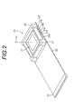
- FIG. 2 is an external perspective view of the imaging module 100 shown in FIG. 1 with the lens unit 10 omitted.
- the image sensor unit 20 includes a substrate 21 on which an image sensor 27 such as a CCD (Charge-Coupled Device) image sensor or a CMOS (Complementary Metal-Oxide-Semiconductor) image sensor is formed, And a flexible substrate 22 connected to.
- an image sensor 27 such as a CCD (Charge-Coupled Device) image sensor or a CMOS (Complementary Metal-Oxide-Semiconductor) image sensor is formed
- CMOS Complementary Metal-Oxide-Semiconductor
- the outer edge shape of the image sensor 27 is a rectangle (not limited to a complete rectangle but substantially a rectangle).
- two parallel sides of the four main sides constituting the outer edge of the imaging device 27 are parallel to the x direction, and the remaining two sides are parallel to the y direction. It has become.
- the pixel pitch of the image sensor 27 is not particularly limited, but an image sensor having a pixel pitch of 1 ⁇ m or less is used as the image sensor 27.
- the pixel pitch refers to the smallest distance among the distances between the centers of the photoelectric conversion regions included in the pixels included in the image sensor 27.
- the pixel pitch of the image sensor has become narrower.
- the area per pixel is reduced.
- the radius of the allowable circle of confusion is reduced and the depth of focus is reduced.
- the F number of the lens tends to decrease.
- the focal depth of recent imaging modules is very shallow, it is required to align the lens unit and the imaging element unit with high accuracy.
- the pixel pitch is 1 ⁇ m or less, particularly high alignment accuracy is required.
- a cylindrical cover holder 25 is formed on the substrate 21, and an image sensor 27 is disposed inside the cover holder 25.
- a cover glass (not shown) is fitted in the hollow portion of the cover holder 25 above the image sensor 27.
- an image sensor unit terminal portion including terminals 24A to 24F for electrical connection with the lens unit 10 is provided.
- the image sensor unit terminal portion only some of the terminals are shown in the same manner as the lens unit terminal portion.
- the substrate 21 is provided with an image sensor wiring connected to a data output terminal and a drive terminal of the image sensor 27.
- the imaging element wiring is connected to the external connection terminal portion 23 provided at the end of the flexible substrate 22 via the wiring provided on the flexible substrate 22.
- the external connection terminal portion 23 functions as an electrical connection portion that is electrically connected to the image sensor 27.
- the substrate 21 is provided with a lens unit wiring connected to each terminal included in the image sensor unit terminal portion.
- the lens unit wiring is connected to the external connection terminal portion 23 provided at the end of the flexible substrate 22 via the wiring provided on the flexible substrate 22.
- each terminal of the lens unit terminal unit 14 and each terminal of the image sensor unit terminal unit corresponding thereto are electrically connected. .
- terminal 14A and the terminal 24A are electrically connected, the terminal 14B and the terminal 24B are electrically connected, the terminal 14C and the terminal 24C are electrically connected, and the terminal 14D and the terminal 24D are connected.
- the terminals 14E and 24E are electrically connected, and the terminals 14F and 24F are electrically connected.
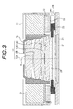
- FIG. 3 is a cross-sectional view taken along line AA of the imaging module 100 shown in FIG.
- the image sensor 27 is disposed in a recess provided in the substrate 21 and is sealed by a cover holder 25 provided on the substrate 21 and a cover glass 26 fitted in the cover holder 25. ing.
- the lens unit 10 includes a lens group 12 including a plurality of lenses (four lenses 12A to 12D in the example of FIG. 3) disposed above the cover glass 26, and supports the lens group 12. And a cylindrical lens barrel 15.
- the lens unit 10 also includes a bottom block 19 placed on the upper surface of the cover holder 25 of the image sensor unit 20 and a flexible substrate 13 fixed on the bottom block 19.
- the lens unit 10 includes a lens unit terminal portion connected to the flexible substrate 13 (only the terminal 14C is shown in FIG. 3 because of a cross section), and a lens driving device 16 formed above the flexible substrate 13. .
- the lens group 12, the lens barrel 15, the bottom block 19, the flexible substrate 13, and the lens driving device 16 are accommodated in the housing 11.
- the lens driving device 16 includes a first lens driving unit, a second lens driving unit, a third lens driving unit, and a Hall element as a position detection element that detects the position of the lens.
- the first lens driving unit sets at least a part of the lenses in the lens group 12 (all the lenses in the lens group 12 in the example of FIG. 3) in a first direction along the optical axis Ax of the lens group 12 ( It is a drive unit for performing focus adjustment by moving in the z direction in FIG.
- the second lens driving unit and the third lens driving unit have at least some of the lenses in the lens group 12 (all the lenses in the lens group 12 in the example of FIG. 3) as the optical axis Ax of the lens group 12. It is a drive unit for correcting blurring of an image picked up by the image sensor 27 by moving in a second direction (x direction in FIG. 1) and a third direction (y direction in FIG. 1) orthogonal to each other.
- the first lens driving unit, the second lens driving unit, and the third lens driving unit are actuators for moving the lens, respectively.
- a voice coil motor VCM
- Other known means may be employed.
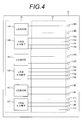
- FIG. 4 is a block diagram showing an electrical connection configuration of the lens unit 10 shown in FIG.
- the lens driving device 16 detects an x-direction VCM 16A (the second lens driving unit) for moving the lens group 12 in the x direction and a position of the lens group 12 in the x direction. and an x-direction hall element 16B.
- the lens driving device 16 includes a y-direction VCM 16C (the third lens driving unit) for moving the lens group 12 in the y direction, and a y-direction hall element 16D for detecting the y-direction position of the lens group 12.
- the lens driving device 16 includes a z-direction VCM 16E (the first lens driving unit) for moving the lens group 12 in the z-direction and a z-direction hall element for detecting the z-direction position of the lens group 12. 16F.
- VCM 16E the first lens driving unit
- a z-direction hall element for detecting the z-direction position of the lens group 12. 16F.
- the x-direction VCM 16A has two terminals, and each of the two terminals is electrically connected to the terminal 14A and the terminal 14B via a wiring formed on the flexible substrate 13.
- the x-direction hall element 16B has four terminals, and each of the four terminals is electrically connected to the terminal 14a, the terminal 14b, the terminal 14c, and the terminal 14d through a wiring formed on the flexible substrate 13. ing.
- the y-direction VCM 16C has two terminals, and each of the two terminals is electrically connected to the terminal 14C and the terminal 14D through wiring formed on the flexible substrate 13.
- the y-direction hall element 16D has four terminals, and each of the four terminals is electrically connected to the terminal 14e, the terminal 14f, the terminal 14g, and the terminal 14h via wiring formed on the flexible substrate 13. ing.
- each of the two terminals is electrically connected to the terminal 14E and the terminal 14F via a wiring formed on the flexible substrate 13.
- the z-direction hall element 16F has four terminals, and each of the four terminals is electrically connected to the terminal 14i, the terminal 14j, the terminal 14k, and the terminal 14l through the wiring formed on the flexible substrate 13. ing.
- the number of terminals required for each lens driving unit and each Hall element is an example, and is not limited to the above.
- the lens unit 10 and the imaging element unit 20 are separately manufactured. Then, an adjustment process for aligning the lens unit 10 and the image sensor unit 20 is performed so that the imaging surface of the subject imaged by the lens group 12 coincides with the image pickup surface of the image sensor 27, and then the lens. The unit 10 and the image sensor unit 20 are bonded and fixed.
- the lens unit 10 and the image sensor unit 20 are aligned by moving the image sensor unit 20 with the lens unit 10 held in a predetermined posture by the manufacturing apparatus. At this time, the lens unit 10 is held in such a posture that the z direction shown in FIG. 1 is parallel to the gravity direction, and the x direction and the y direction are perpendicular to the gravity direction.
- the posture of the lens unit 10 in which the x direction and the y direction are perpendicular to the gravitational direction may be any posture such that the lens group 12 does not move in the x direction and the y direction due to the influence of gravity.
- the y direction and the gravity direction need not be strictly perpendicular. For example, as long as the lens group 12 does not move in the x and y directions, the tilt of the lens unit 10 due to mechanical loss, frictional resistance, or the like is allowed.
- the lens group 12 is movable in the z direction by the first lens driving unit (z direction VCM 16E). Therefore, if the lens unit 10 is held in a posture in which the z direction is parallel to the gravity direction, the position of the lens group 12 in the z direction is affected by gravity, and thus it is assumed that the lens unit 12 is deviated from the reference position for alignment.
- the initial positions of the lens group 12 in the x and y directions are the optical axis Ax and the center of the imaging surface of the imaging element 27. Ideally, the positions should match.
- the initial position of the lens group 12 in the z direction may be any position.
- the positions of the lens group 12 in the x direction and the y direction are not affected by gravity.
- the direction position and the y-direction position can be matched with the initial position in use.
- the z-direction position of the lens group 12 is affected by gravity, there is a problem even if the z-direction position of the held lens group 12 is different from the initial z-direction position of the lens group 12 in use. Absent.
- the first lens driving is performed by moving the image pickup device unit 20 while holding the lens unit 10 in a posture in which the z direction is parallel to the gravity direction and aligning the lens unit 10 and the image pickup device unit 20.
- High-precision alignment is possible without driving the second lens driving unit, the second lens driving unit, and the third lens driving unit.
- the z direction position of the lens group 12 is
- the lens unit 10 may be designed to be the end at infinity or the closest end. This makes it easier to align the lens unit 10 and the image sensor unit 20.
- the x-direction position and the y-direction position of the lens group 12 slightly deviate from the initial position during use due to assembly errors or the like even when the lens unit 10 is held in a posture in which the z direction is parallel to the gravity direction. there is a possibility.
- the second lens driving unit (x direction VCM 16A) and the third lens driving unit (y direction VCM 16C) are energized to drive the second lens driving unit and the third lens driving unit.
- the lens unit 10 and the image sensor unit 20 may be aligned. As a result, more accurate alignment is possible.
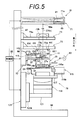
- FIG. 5 is a side view showing a schematic configuration of the manufacturing apparatus 200 for the imaging module 100.
- the imaging module manufacturing apparatus 200 completes the imaging module 100 by adjusting the position and inclination of the imaging device unit 20 with respect to the lens unit 10 and fixing the imaging device unit 20 to the lens unit 10 after the adjustment.
- the imaging module manufacturing apparatus 200 includes a chart unit 71, a condensing unit 73, a lens positioning plate 75, a lens holding mechanism 77, an imaging element unit holding unit 79, an adhesive supply unit 81, an ultraviolet lamp 83, And a control unit 85 for controlling them.
- the common work table 86 is fixed to a surface 87 parallel to the direction of gravity.
- the chart unit 71 includes a box-shaped casing 71a, a measurement chart 89 fitted in the casing 71a, and a light source 91 that is incorporated in the casing 71a and illuminates the measurement chart 89 from the back with parallel light. It is configured.
- the measurement chart 89 is formed of, for example, a plastic plate having light diffusibility.
- the chart surface of the measurement chart 89 is perpendicular to the direction of gravity.
- FIG. 6 is a diagram showing a chart surface of the measurement chart 89.
- the measurement chart 89 has a rectangular shape, and a plurality of chart images CH1, CH2, CH3, CH4, and CH5 are printed on the chart surface on which the chart pattern is provided.
- the plurality of chart images are all the same image, and are so-called ladder-like chart patterns in which black lines are arranged at predetermined intervals.
- Each chart image is composed of a horizontal chart image Px arranged in the horizontal direction of the image and a vertical chart image Py arranged in the vertical direction of the image.
- the condensing unit 73 is arranged to face the chart unit 71 on the Z axis, which is a perpendicular to the chart surface of the measurement chart 89 and passes through the chart surface center 89a.
- the condensing unit 73 includes a bracket 73a and a condensing lens 73b fixed to the surface 87 of the work table 86.
- the condensing lens 73b condenses the light emitted from the chart unit 71 and causes the condensed light to enter the lens unit 10 through the opening 73c formed in the bracket 73a.
- the lens positioning plate 75 is formed to have rigidity, for example, by metal, and is provided with an opening 75a through which the light collected by the light collecting unit 73 passes.
- the lens positioning plate 75 is disposed facing the light collecting unit 73 on the Z axis.
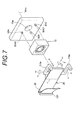
- FIG. 7 is an explanatory diagram showing a holding state of the lens unit 10 and the imaging element unit 20 by the imaging module manufacturing apparatus 200.
- three contact pins 93A, 93B, and 93C are provided around the opening 75a.
- insertion pins 93A1, 93C1 having a smaller diameter than the contact pins are provided at the tips of the two contact pins 93A, 93C arranged diagonally. Yes.
- the contact pins 93A, 93B, 93C receive the recesses 95A, 95B, 95C of the lens unit 10 shown in FIG. 1, and the insertion pins 93A1, 93C1 are inserted into the recesses 95C1, 95A1 to position the lens unit 10.
- the Z axis coincides with the optical axis Ax of the lens unit 10. That is, in the lens unit 10, the x direction and the y direction in FIG. 1 are perpendicular to the gravity direction, and the z direction is parallel to the gravity direction.
- the lens holding mechanism 77 includes a holding plate 97 that holds the lens unit 10 so that the top plate of the housing 11 faces the chart unit 71 on the Z axis, and a first slide stage that moves the holding plate 97 in the Z axis direction. 99.
- the first slide stage 99 is an electric precision stage that rotates a ball screw by the rotation of a motor (not shown) and moves the stage portion 99a engaged with the ball screw in the Z-axis direction.
- the lens unit 10 is held by the manufacturing apparatus 200. Become.
- the lens positioning plate 75 and the lens holding mechanism 77 constitute a lens unit holding portion that holds the lens unit 10 on the Z axis in a state where the x direction and the y direction are perpendicular to the gravity direction.
- a probe unit 113 including four probe pins 113a, 113b, 113c, and 113d is attached to the stage portion 99a so as to face the holding plate 97.
- the probe pin 113a is brought into contact with the terminal 14A of the lens unit 10
- the probe pin 113b is brought into contact with the terminal 14B of the lens unit 10
- the probe pin 113c is brought into contact with the terminal 14C of the lens unit 10. 1
- the probe pin 113d is brought into contact with the 0 terminal 14D, and the terminals 14A, 14B, 14C, and 14D are energized, whereby the second lens driving unit (x direction VCM 16A) and the third lens driving unit (y direction VCM 16C). Drive.
- the probe unit 113 functions as an energization unit that energizes the terminals 14A to 14D to drive the second lens driving unit and the third lens driving unit based on a command from the control unit 85.
- the probe unit 113 drives the second lens driving unit and the third lens driving unit so that the x-direction position and the y-direction position of the lens group 12 of the lens unit 10 are the initial positions in use, and the lens unit 10 The position of the lens group 12 of the unit 10 is adjusted.
- the image sensor unit holding unit 79 holds the image sensor unit 20 on the Z axis. Further, the image sensor unit holding unit 79 can change the position and inclination of the image sensor unit 20 in the Z-axis direction under the control of the control unit 85.
- the inclination of the imaging element unit 20 means the inclination of the imaging surface 27a of the imaging element 27 with respect to a plane orthogonal to the Z axis.
- the image sensor unit holding unit 79 includes a chuck hand 115, a biaxial rotation stage 119, and a second slide stage 123.
- the chuck hand 115 holds the imaging element unit 20 so that the imaging surface 27a faces the chart unit 71 on the Z axis.
- the biaxial rotation stage 119 holds a substantially crank-shaped bracket 117 to which the chuck hand 115 is attached, and tilts the image sensor unit 20 around two axes (horizontal X axis and vertical Y axis) perpendicular to the Z axis. adjust.
- the second slide stage 123 holds the bracket 121 to which the biaxial rotation stage 119 is attached, and moves the bracket 121 in the Z-axis direction. That is, the biaxial rotation stage and the second slide stage 123 constitute an adjustment unit that adjusts at least the Z-axis direction position of the image sensor unit 20 with respect to the lens unit 10.
- the chuck hand 115 includes a pair of sandwiching members 115a bent in a substantially crank shape, and an actuator 115b that moves these sandwiching members 115a in the X-axis direction orthogonal to the Z-axis (see FIG. 5). It consists of and.
- the sandwiching member 115 a sandwiches the outer frame of the image sensor unit 20 and holds the image sensor unit 20.
- the chuck hand 115 positions the image pickup device unit 20 held by the holding member 115a so that the optical axis Ax of the lens unit 10 and the center position of the image pickup surface 27a substantially coincide with each other.
- the chuck hand 115 is configured such that each terminal of the imaging element unit terminal portion of the imaging element unit 20 and each terminal of the lens unit terminal portion of the held lens unit 10 overlap each other. Then, the image sensor unit 20 sandwiched between the sandwiching members 115a is positioned.
- the two-axis rotary stage 119 is an electric two-axis goniometer stage, and the rotation of two motors (not shown) causes the image sensor unit 20 to move around the X axis about the center position of the image pickup surface 27a. It is inclined in the ⁇ x direction and the ⁇ y direction around the Y axis perpendicular to the Z axis and the X axis. Thereby, when the imaging element unit 20 is tilted in each direction, the positional relationship between the center position of the imaging surface 27a and the Z axis does not shift.
- the second slide stage 123 is an electric precision stage that rotates a ball screw by rotation of a motor (not shown) and moves a stage portion 123a engaged with the ball screw in the Z-axis direction.
- a bracket 121 is fixed to the stage portion 123a.
- the connector cable 127 connected to the external connection terminal portion 23 provided at the tip of the flexible substrate 22 of the image sensor unit 20 is attached to the biaxial rotation stage 119.
- the connector cable 127 inputs a drive signal to the image sensor 27 and outputs an image signal output from the image sensor 27.
- the adhesive supply unit 81 and the ultraviolet lamp 83 constitute a unit fixing unit that fixes the lens unit 10 and the image sensor unit 20.
- the adhesive supply unit 81 supplies the ultraviolet curable adhesive to the gap between the lens unit 10 and the image sensor unit 20 after the adjustment of the position and inclination between the lens unit 10 and the image sensor unit 20 is completed.
- the ultraviolet lamp 83 cures the adhesive by irradiating the ultraviolet curable adhesive supplied to the gap with ultraviolet rays.
- the adhesive in addition to the ultraviolet curable adhesive, an instantaneous adhesive, a thermosetting adhesive, a natural curable adhesive, and the like can be used.
- FIG. 8 is a block diagram showing the internal configuration of the imaging module manufacturing apparatus 200.
- each unit described above is connected to the control unit 85.
- the control unit 85 is, for example, a microcomputer including a CPU, a ROM, a RAM, and the like, and controls each unit based on a control program stored in the ROM.
- the control unit 85 is connected to an input unit 131 such as a keyboard and a mouse for performing various settings, and a display unit 133 that displays setting contents, work contents, work results, and the like.
- the lens driving driver 145 is a driving circuit for driving the second lens driving unit and the third lens driving unit, and is driven to the second lens driving unit and the third lens driving unit via the probe unit 113.
- the image sensor driver 147 is a drive circuit for driving the image sensor 27, and inputs a drive signal to the image sensor 27 via the connector cable 127.
- the in-focus coordinate value acquisition circuit 149 performs Z for a plurality of imaging positions (positions corresponding to the chart images CH1, CH2, CH3, CH4, and CH5 of the measurement chart 89) set on the imaging surface 27a of the imaging element 27. In-focus coordinate values that are positions with a high degree of focus in the axial direction are acquired.
- the control unit 85 controls the second slide stage 123 when acquiring the in-focus coordinate values of a plurality of imaging positions, and a plurality of measurement positions (Z0, Z1, Z2) discretely set in advance on the Z axis. ,... Are sequentially moved. Further, the control unit 85 controls the image sensor driver 147 to display chart images of a plurality of chart images CH1, CH2, CH3, CH4, and CH5 of the measurement chart 89 formed by the lens group 12 at each measurement position. Let's take an image.
- the focused coordinate value acquisition circuit 149 extracts pixel signals corresponding to the plurality of imaging positions from the imaging signal input via the connector cable 127, and individually focuses evaluation on the plurality of imaging positions from the pixel signals. Each value is calculated.
- the measurement position when a predetermined focus evaluation value is obtained for each imaging position is set as a focus coordinate value on the Z axis.
- a contrast transfer function value (hereinafter referred to as CTF value) can be used.
- the CTF value is a value representing the contrast of the image with respect to the spatial frequency, and when the CTF value is high, the degree of focus is considered high.
- the in-focus coordinate value acquisition circuit 149 has a plurality of directions set on the XY coordinate plane for each of a plurality of measurement positions (Z0, Z1, Z2,...) Set on the Z axis for each of a plurality of imaging positions. CTF values are calculated for each.
- the direction in which the CTF value is calculated is, for example, a horizontal direction (X-axis direction) that is the horizontal direction of the imaging surface 27a and a vertical direction (Y-axis direction) orthogonal thereto, and the CTF value in each direction is X -CTF value and Y-CTF value are calculated respectively.
- the in-focus coordinate value acquisition circuit 149 for a plurality of imaging positions corresponding to each chart image CH1, CH2, CH3, CH4, CH5, coordinates on the Z axis (Zp1, Zp2) of the measurement position where the X-CTF value is maximum , Zp3, Zp4, Zp5) are acquired as the horizontal in-focus coordinate values. Similarly, the coordinate on the Z axis of the measurement position where the Y-CTF value is maximized is acquired as the vertical focus coordinate value.
- the image plane calculation circuit 151 receives the horizontal focus coordinate value and the vertical focus coordinate value of each imaging position from the focus coordinate value acquisition circuit 149.
- the imaging plane calculation circuit 151 includes the XY coordinate value of each imaging position when the imaging surface 27a is made to correspond to the XY coordinate plane, the horizontal in-focus coordinate value on the Z axis and the vertical value obtained for each imaging position.
- a plurality of evaluation points expressed in combination with the in-focus coordinate values are expanded into a three-dimensional coordinate system combining the XY coordinate plane and the Z axis, and the three-dimensional coordinate system is based on the relative positions of these evaluation points.
- An approximate imaging plane expressed as one plane is calculated.
- Approximate image plane information is input from the image plane calculation circuit 151 to the adjustment value calculation circuit 153.
- the adjustment value calculation circuit 153 has an imaging plane coordinate value F1 on the Z axis that is an intersection of the approximate imaging plane and the Z axis, and an inclination about the X axis and the Y axis of the approximate imaging plane with respect to the XY coordinate plane.
- a certain XY direction rotation angle is calculated and input to the control unit 85.
- the control unit 85 drives the image sensor unit holding unit 79 based on the imaging plane coordinate value and the XY direction rotation angle input from the adjustment value calculation circuit 153, and adjusts the Z-axis direction position and inclination of the image sensor unit 20. Then, the imaging surface 27a is made to coincide with the approximate imaging surface.
- the imaging module manufacturing apparatus 200 described above generally performs the following steps. (1) The process of holding the lens unit 10 on the Z axis orthogonal to the chart surface of the measurement chart 79 in a state where the x direction and the y direction are perpendicular to the direction of gravity, and holding the image sensor unit 20 on the Z axis. 2) The Z-axis direction position of the image sensor unit 20 held on the Z axis is changed, and the second lens driving unit and the third lens driving unit of the lens unit 10 held on the Z axis at each position. (3) Based on the imaging signal obtained by imaging the measurement chart 79 by the imaging device 27. The step of driving the imaging device 27 through the electrical connection portion and imaging the measurement chart 79 by the imaging device 27. Adjusting the position and inclination of the image sensor unit 20 with respect to the lens unit 10 and fixing the image sensor unit 20 to the lens unit 10.
- the control unit 85 controls the first slide stage 99 to move the holding plate 97 along the Z-axis direction, thereby providing a space in which the lens unit 10 can be inserted between the lens positioning plate 75 and the holding plate 97.
- the lens unit 10 is held by a robot (not shown) and transferred between the lens positioning plate 75 and the holding plate 97.
- the control unit 85 detects the movement of the lens unit 10 with an optical sensor or the like, and moves the stage unit 99a of the first slide stage 99 in a direction approaching the lens positioning plate 75. As a result, the holding plate 97 holds the lens unit 10.
- the probe unit 113 contacts the terminals 14 ⁇ / b> A and 14 ⁇ / b> B of the lens unit 10 and electrically connects the second lens driving unit and the lens driving driver 145.
- the holding plate 97 After releasing the holding of the lens unit 10 by a robot (not shown), the holding plate 97 is further moved toward the lens positioning plate 75. Then, the concave portions 95A, 95B, and 95C of the lens unit 10 come into contact with the contact pins 93A, 93B, and 93C, and the insertion pins 93A1 and 93C1 are inserted into the concave portions 95C1 and 95A1. Accordingly, the lens unit 10 is positioned in the Z-axis direction, the X-axis direction, and the Y-axis direction.
- the control unit 85 controls the second slide stage 123 to move the biaxial rotary stage 119 along the Z-axis direction, so that the image sensor unit 20 is inserted between the holding plate 97 and the biaxial rotary stage 119. Create possible space.
- the image sensor unit 20 is held by a robot (not shown) and transferred between the holding plate 97 and the biaxial rotation stage 119.
- the control unit 85 detects the movement of the image sensor unit 20 with an optical sensor or the like, and moves the stage unit 123a of the second slide stage 123 in the direction approaching the holding plate 97. Then, the operator holds the image sensor unit 20 using the clamping member 115 a of the chuck hand 115.
- the connector cable 127 is connected to the external connection terminal portion 23 of the image sensor unit 20. Thereby, the image sensor 27 and the control unit 85 are electrically connected. Thereafter, the holding of the image sensor unit 20 by a robot (not shown) is released.
- the focus coordinate value acquisition circuit 149 causes the horizontal focus coordinate value and the vertical focus coordinate value of each image pickup position on the image pickup surface 27a. Is acquired (S3).
- control unit 85 controls the second slide stage 123 to move the biaxial rotation stage 119 in a direction approaching the lens holding mechanism 77, and the first measurement in which the image sensor 27 is closest to the lens unit 10.
- the image sensor unit 20 is moved to the position.
- Control unit 85 causes light source 91 of chart unit 71 to emit light.
- the control unit 85 inputs a drive signal from the lens drive driver 145 to the terminals 14A, 14B, 14C, and 14D, and drives the second lens drive unit and the third lens drive unit to
- the x-direction position and the y-direction position of the optical axis Ax are held at the reference position (for example, the initial position during actual use).
- control unit 85 controls the image sensor driver 147 to cause the image sensor 27 to capture the chart images CH1, CH2, CH3, CH4, and CH5 formed by the lens unit 10.
- the image sensor 27 inputs the captured image signal to the focused coordinate value acquisition circuit 149 via the connector cable 127.
- the in-focus coordinate value acquisition circuit 149 extracts the pixel signal at the imaging position corresponding to each chart image CH1, CH2, CH3, CH4, and CH5 from the input imaging signal, and X for each imaging position from the pixel signal. -Calculate CTF and Y-CTF values.
- the control unit 85 stores information on the X-CTF value and the Y-CTF value in, for example, a RAM in the control unit 85.
- the control unit 85 sequentially moves the image sensor unit 20 to a plurality of measurement positions (Z0, Z1, Z2,%) Set along the Z-axis direction, and the optical axis Ax of the lens group 12 at each measurement position.
- the image sensor 27 is caused to capture the chart image of the measurement chart 89 in a state where the x-direction position and the y-direction position are held at the reference position.
- the focused coordinate value acquisition circuit 149 calculates an X-CTF value and a Y-CTF value at each imaging position at each measurement position.
- the focused coordinate value acquisition circuit 149 selects the maximum value from among the plurality of calculated X-CTF values and Y-CTF values for each of the imaging positions, and the Z-axis of the measurement position where the maximum value is obtained.
- the coordinates are acquired as the horizontal focus coordinate value and the vertical focus coordinate value of the imaging position.
- the horizontal focus coordinate value and the vertical focus coordinate value acquired by the focus coordinate value acquisition circuit 149 are input to the imaging plane calculation circuit 151.
- the imaging plane calculation circuit 151 calculates the approximate imaging plane F that is approximated by a plane, for example, by the method of least squares (S5).
- the adjustment value calculation circuit 153 includes an imaging plane coordinate value F1 that is an intersection of the approximate imaging plane F and the Z axis, and an XY direction that is an inclination around the X axis and the Y axis of the approximate imaging plane with respect to the XY coordinate plane.
- the rotation angle is calculated and input to the controller 85 (S6).
- the control unit 85 controls the biaxial rotation stage 119 and the second slide stage 123 based on the imaging plane coordinate value F1 and the rotation angle in the XY direction, and the center position of the imaging plane 27a of the imaging element 27 is the imaging plane coordinate.
- the image sensor unit 20 is moved in the Z-axis direction so as to coincide with the value F1, and the angles of the ⁇ x direction and ⁇ y direction of the image sensor unit 20 are adjusted so that the inclination of the image sensing surface 27a coincides with the approximate imaging plane F. Adjust (S7).
- the control unit 85 performs a confirmation process of confirming the in-focus position of each imaging position after the position adjustment of the imaging element unit 20 (S8). In this confirmation step, each step of S3 described above is executed again. After the position adjustment of the image sensor unit 20, the variation in the evaluation value corresponding to each of the image pickup positions in the horizontal direction and the vertical direction becomes small.
- the control unit 85 moves the image sensor unit 20 in the Z-axis direction so that the center position of the imaging surface 27a coincides with the imaging plane coordinate value F1 after the confirmation step (S8) is completed (S4) (S9). Further, the control unit 85 supplies an ultraviolet curable adhesive to the gap between the lens unit 10 and the imaging element unit 20 from the adhesive supply unit 81 (S10), and turns on the ultraviolet lamp 83, thereby activating the ultraviolet curable adhesive. The agent is cured (S11).
- the completed imaging module 100 is taken out from the imaging module manufacturing apparatus 200 by a robot (not shown) (S12).
- the lens unit 10 and the image sensor unit 20 can be fixed with an ultraviolet curable adhesive, but curing with the ultraviolet curable adhesive may be used as temporary fixing between the lens unit 10 and the image sensor unit 20.
- the imaging module 100 is removed from the imaging module manufacturing apparatus 200 in a state where the lens unit 10 and the imaging element unit 20 are temporarily fixed, and after performing a desired process such as a cleaning process, the lens unit 10 and the imaging element unit 20 May be completely fixed by a thermosetting adhesive or the like.
- the lens unit 10 and the imaging element unit 20 can be aligned with high accuracy.
- the probe unit 113 may be omitted. According to this configuration, when the lens unit 10 and the image sensor unit 20 are aligned, it is not necessary to energize the lens unit 10. For this reason, the cost of the manufacturing apparatus 200 can be reduced and the imaging module 100 can be manufactured at low cost.
- the second lens driving unit and the third lens driving unit included in the lens unit 10 are driven to enable highly accurate alignment.
- the measurement chart 89 may be imaged by the imaging element 27 at each measurement position while the Hall element included in the lens driving device 16 is energized.
- the probe unit 113 of the manufacturing apparatus 200 is in contact with the probe that contacts the four terminals 14a to 14d connected to the x-direction hall element 16B and the four terminals 14e to 14h that are connected to the y-direction hall element 16D. And a probe.
- the terminals 14a to 14d are energized at each measurement position, and the x-direction position of the lens group 12 is held with high accuracy using the detection signal of the x-direction hall element 16B.
- 14e to 14h may be energized, and imaging may be performed in a state where the y-direction position of the lens group 12 is held with high accuracy using the detection signal of the y-direction hall element 16D.
- (Third modification) A mode in which the position of the lens group 12 is adjusted by energizing the terminals that are energized during actual use when the lens unit 10 and the image sensor unit 20 are aligned using the manufacturing apparatus 200 of FIG. .
- the lens unit 10 may be provided with a dedicated terminal for energizing when performing alignment.
- the lens group 12 may be controlled to a desired position by energizing the dedicated terminal from the probe unit 113, and the process of S3 in FIG. 9 may be performed.
- the design freedom of the probe unit 113 can be improved by using a dedicated terminal.
- the coordinate position value is acquired at each measurement position by changing the measurement position by moving the imaging element unit 20 while the Z-axis direction position of the lens unit 10 is fixed.
- the lens unit 10 can be moved in the Z-axis direction, and the lens unit 10 is moved in the Z-axis direction while the position of the image sensor unit 20 in the Z-axis direction is fixed, or the lens unit 10
- the imaging element unit 20 may be moved in the Z-axis direction to change the measurement position, and the in-focus coordinate value may be acquired at each measurement position.
- the measurement position is changed by moving the measurement chart 89 in the Z-axis direction, and the in-focus coordinate value at each measurement position is acquired. Also good.
- the focus coordinate value at each measurement position may be acquired by changing the measurement position by changing the Z-axis direction position of each of the lens unit 10, the image sensor unit 20, and the measurement chart 89.
- the measurement position is changed by changing the relative position in the Z-axis direction of the lens unit 10, the image sensor unit 20, and the measurement chart 89, and the measurement chart 89 is imaged by the image sensor 27 at each relative position to be focused. Any configuration that acquires coordinate values may be used.
- a mode has been described in which a plurality of measurement positions are realized by changing the relative position, and a measurement chart is imaged when each measurement position is reached.
- the measurement chart may be continuously imaged (that is, moving image imaging is performed), and the relative position may be changed so that each measurement position is obtained during the imaging.
- the Z-axis direction position of the image sensor unit 20 with respect to the lens unit 10 is adjusted by moving the image sensor unit 20 while the Z-axis direction position of the lens unit 10 is fixed.
- the lens unit 10 is made movable in the Z-axis direction, and the image sensor unit 20 is moved while the position is fixed, or the lens unit 10 and the image sensor unit 20 are moved respectively. By adjusting the position, the position may be adjusted.
- the second lens driving unit and the third lens of the lens unit 10 are used. By energizing the drive unit, high-accuracy alignment is possible.
- the tilt adjustment of the image sensor unit 20 with respect to the lens unit 10 can be performed with higher accuracy.
- a manufacturing method of an imaging module having a lens unit having a lens group and an imaging element unit having an imaging element fixed to the lens unit and imaging a subject through the lens group is disclosed.
- the lens unit includes: a first lens driving unit that moves at least a part of the lenses in the lens group in a first direction along an optical axis of the lens group; and at least a part of the lenses in the lens group.
- a second lens driving unit and a third lens driving unit that respectively move in a second direction and a third direction orthogonal to the optical axis of the lens group;
- the image sensor unit includes an electrical connection portion that is electrically connected to the image sensor.
- the method of manufacturing the imaging module includes: holding the lens unit on an axis orthogonal to the measurement chart; and holding the lens unit in a state where the second direction and the third direction are perpendicular to the direction of gravity.
- the first step of holding the image sensor unit, the lens unit held on the axis, the image sensor unit, and the relative position in the direction of the axis of the measurement chart are changed, and the relative position in each relative position
- the lens unit based on a second step of driving the imaging device via an electrical connection and imaging the measurement chart by the imaging device, and an imaging signal obtained by imaging the measurement chart by the imaging device And at least the relative position of the image sensor unit in the direction of the axis, and fixing the image sensor unit to the lens unit. And about.
- the measurement chart is imaged by the imaging element in a state where the second lens driving unit and the third lens driving unit of the held lens unit are energized. May be.
- the first unit A lens unit in which the position of the lens group driven by the lens driving unit in the optical axis direction is the infinity end or the closest end may be prepared.
- the tilt of the image sensor unit with respect to the lens unit and the relative position of the lens unit and the image sensor in the axial direction may be adjusted based on the image signal.
- the pixel pitch of the image sensor may be 1.0 ⁇ m or less.
- An imaging module manufacturing apparatus having a lens unit having a lens group and an image sensor unit having an image sensor that is fixed to the lens unit and images a subject through the lens group.
- the lens unit includes a first lens driving unit that moves at least a part of the lenses in the direction along the optical axis of the lens group, and at least a part of the lenses in the lens group.
- a second lens driving unit and a third lens driving unit that move in a second direction and a third direction orthogonal to the optical axis of the first lens driving unit.
- the image sensor unit has an electrical connection part electrically connected to the image sensor.
- the imaging module manufacturing apparatus includes a measurement chart, an imaging element unit holding unit that holds the imaging element unit on an axis orthogonal to the measurement chart, and the measurement chart and the imaging element unit holding unit on the axis.
- the lens unit holding unit, the lens unit holding unit, and the image sensor unit holding unit are arranged between the lens unit and the lens unit holding unit to hold the lens unit in a state where the second direction and the third direction are perpendicular to the gravitational direction.
- the relative position of the measurement chart in the direction of the axis is changed, and at each relative position, the imaging element is driven via the electrical connection part of the imaging element unit, and the measurement chart is measured by the imaging element.
- the lens unit based on an imaging signal obtained by imaging the measurement chart with the imaging device.
- An adjustment unit that adjusts at least the relative position of the image sensor unit in the direction of the axis, and the image sensor unit and the lens unit that are adjusted at least in the relative direction of the axis by the adjustment unit.
- a unit fixing portion to be
- the disclosed imaging module manufacturing apparatus includes an energization unit that energizes the second lens driving unit and the third lens driving unit of the lens unit, and the control unit includes the energization unit at each relative position.
- the measurement chart may be imaged by the imaging element in a state where the second lens driving unit and the third lens driving unit are energized.
- the adjusting unit may adjust the inclination of the imaging element unit with respect to the lens unit and the relative position and inclination of the lens unit and the imaging element unit in the axis direction based on the imaging signal. .
- the method for manufacturing an imaging module according to the present invention is particularly effective when applied to the manufacturing of an imaging module mounted on an electronic device such as a mobile phone, a spectacle-type electronic device, and a wristwatch-type electronic device.
- Imaging module 10 Lens unit 11 Housing
- Imaging element unit 21 Substrate 22 Flexible substrate 23
- Imaging module manufacturing apparatus Ax Optical axis z Direction along optical axis x z direction orthogonal Direction yz direction orthogonal to z direction
Landscapes
- Engineering & Computer Science (AREA)
- Multimedia (AREA)
- Signal Processing (AREA)
- Physics & Mathematics (AREA)
- Health & Medical Sciences (AREA)
- Biomedical Technology (AREA)
- General Health & Medical Sciences (AREA)
- General Physics & Mathematics (AREA)
- Optics & Photonics (AREA)
- Studio Devices (AREA)
- Lens Barrels (AREA)
Abstract
Description
0の端子14Dにプローブピン113dを接触させて、端子14A,14B,14C,14Dに通電することにより、第二のレンズ駆動部(x方向VCM16A)及び第三のレンズ駆動部(y方向VCM16C)を駆動する。
(1)測定チャート79のチャート面に直交するZ軸上にx方向及びy方向が重力方向と垂直になる状態でレンズユニット10を保持し、Z軸上に撮像素子ユニット20を保持する工程
(2)Z軸上に保持された撮像素子ユニット20のZ軸方向位置を変化させ、各位置において、Z軸上に保持されたレンズユニット10の第二のレンズ駆動部及び第三のレンズ駆動部に通電した状態で、電気接続部を介して撮像素子27を駆動して撮像素子27により測定チャート79を撮像させる工程
(3)撮像素子27により測定チャート79を撮像して得られる撮像信号に基づいて、レンズユニット10に対する撮像素子ユニット20のZ軸方向位置及び傾きを調整し、撮像素子ユニット20をレンズユニット10に固定する工程
図5に示した製造装置200において、プローブユニット113は省略した構成としてもよい。この構成によれば、レンズユニット10と撮像素子ユニット20の位置合わせを行う際に、レンズユニット10への通電が不要になる。このため、製造装置200のコストを削減することができ、撮像モジュール100を安価に製造することができる。
上述の実施形態において、レンズユニット10に含まれる第二のレンズ駆動部及び第三のレンズ駆動部を駆動することにより、高精度の位置合わせを可能にしている。より精度を上げるために、レンズ駆動装置16に含まれるホール素子にも通電した状態で、各測定位置において撮像素子27により測定チャート89を撮像させてもよい。
図5の製造装置200を用いてレンズユニット10と撮像素子ユニット20の位置合わせを行う際に、実際の使用時に通電される端子に通電して、レンズ群12の位置を調整する態様を述べた。これに限らず、例えば、位置合わせを行う際に通電するための専用の端子をレンズユニット10に設けておいてもよい。この場合は、この専用の端子にプローブユニット113から通電することで、レンズ群12を所望の位置に制御して、図9のS3の工程を行えばよい。
図9のS3の工程では、レンズユニット10のZ軸方向位置は固定のまま、撮像素子ユニット20を動かしていくことにより、測定位置を変えて、各測定位置で合焦座標値を取得する態様を述べた。これに代えて、レンズユニット10をZ軸方向に移動可能にしておき、撮像素子ユニット20のZ軸方向位置は固定のままレンズユニット10をZ軸方向に移動さることにより、あるいは、レンズユニット10と撮像素子ユニット20をそれぞれZ軸方向に移動させることにより測定位置を変えて、各測定位置で合焦座標値を取得してもよい。
10 レンズユニット
11 筐体
12 レンズ群
13 フレキシブル基板
14A~14F レンズユニット端子部
16 レンズ駆動装置
16A x方向VCM
16B x方向ホール素子
16C y方向VCM
16D y方向ホール素子
16E z方向VCM
16F z方向ホール素子
20 撮像素子ユニット
21 基板
22 フレキシブル基板
23 外部接続用端子
24A~24F 撮像素子ユニット端子部
27 撮像素子
200 撮像モジュール製造装置
Ax 光軸
z 光軸に沿う方向
x z方向に直交する方向
y z方向に直交する方向
Claims (8)
- 撮像モジュールの製造方法であって、
前記撮像モジュールは、レンズ群を有するレンズユニットと、前記レンズユニットに固定され、前記レンズ群を通して被写体を撮像する撮像素子を有する撮像素子ユニットと、を有し、
前記レンズユニットは、前記レンズ群のうち少なくとも一部のレンズを前記レンズ群の光軸に沿う第一の方向に移動させる第一のレンズ駆動部と、前記レンズ群のうち少なくとも一部のレンズを前記レンズ群の光軸に直交する第二の方向及び第三の方向にそれぞれ移動させる第二のレンズ駆動部及び第三のレンズ駆動部と、を有し、
前記撮像素子ユニットは、前記撮像素子と電気的に接続された電気接続部を有し、
測定チャートに直交する軸上に、前記第二の方向及び前記第三の方向が重力方向と垂直になる状態において前記レンズユニットを保持し、かつ、前記軸上に前記撮像素子ユニットを保持する第一工程と、
前記軸上に保持された前記レンズユニット、前記撮像素子ユニット、及び前記測定チャートの前記軸の方向の相対位置を変化させて、各相対位置において前記電気接続部を介して前記撮像素子を駆動して前記撮像素子により前記測定チャートを撮像させる第二工程と、
前記撮像素子により前記測定チャートを撮像して得られる撮像信号に基づいて、前記レンズユニットと前記撮像素子ユニットとの少なくとも前記軸の方向の相対位置を調整し,前記撮像素子ユニットを前記レンズユニットに固定する第三工程と、を備える撮像モジュールの製造方法。
- 請求項1記載の撮像モジュールの製造方法であって、
前記第二工程では、前記各相対位置において、前記保持された前記レンズユニットの前記第二のレンズ駆動部及び前記第三のレンズ駆動部に通電した状態において、前記撮像素子により前記測定チャートを撮像させる撮像モジュールの製造方法。
- 請求項1又は2記載の撮像モジュールの製造方法であって、
前記レンズユニットとして、前記第二の方向及び前記第三の方向が重力方向と垂直になる状態において前記第一のレンズ駆動部に通電を行わずに前記レンズユニットを保持した場合に、前記第一のレンズ駆動部によって駆動される前記レンズ群の光軸方向位置が無限遠端又は最近接端であるレンズユニットを準備する撮像モジュールの製造方法。
- 請求項1~3のいずれか1項記載の撮像モジュールの製造方法であって、
前記第三工程では、前記撮像信号に基づいて、前記レンズユニットに対する前記撮像素子ユニットの傾き、及び、前記レンズユニットと前記撮像素子ユニットとの前記軸の方向の相対位置を調整する撮像モジュールの製造方法。
- 請求項1~4のいずれか1項記載の撮像モジュールの製造方法であって、
前記撮像素子の画素ピッチは1.0μm以下である撮像モジュールの製造方法。
- 撮像モジュールの製造装置であって、
前記撮像モジュールは、レンズ群を有するレンズユニットと、前記レンズユニットに固定され、前記レンズ群を通して被写体を撮像する撮像素子を有する撮像素子ユニットと、を有し、
前記レンズユニットは、前記レンズ群のうち少なくとも一部のレンズを前記レンズ群の光軸に沿う方向に移動させる第一のレンズ駆動部と、前記レンズ群のうち少なくとも一部のレンズを前記レンズ群の光軸に直交する第二の方向及び第三の方向にそれぞれ移動させる第二のレンズ駆動部及び第三のレンズ駆動部と、を有し、
前記撮像素子ユニットは、前記撮像素子と電気的に接続された電気接続部を有し、
前記製造装置は、
測定チャートと、
前記測定チャートに直交する軸上に前記撮像素子ユニットを保持する撮像素子ユニット保持部と、
前記軸上で前記測定チャートと前記撮像素子ユニット保持部との間に配置され、前記第二の方向及び前記第三の方向が重力方向と垂直になる状態において、前記レンズユニットを保持するレンズユニット保持部と、
前記レンズユニット保持部、前記撮像素子ユニット保持部、及び前記測定チャートの前記軸の方向の相対位置を変化させて、各相対位置において、前記撮像素子ユニットの前記電気接続部を介して前記撮像素子を駆動して前記撮像素子により前記測定チャートを撮像させる制御部と、
前記撮像素子により前記測定チャートを撮像して得られる撮像信号に基づいて、前記レンズユニットと前記撮像素子ユニットとの少なくとも前記軸の方向の相対位置を調整する調整部と、
前記調整部により少なくとも前記軸の方向の相対位置を調整された前記撮像素子ユニットと前記レンズユニットとを固定するユニット固定部と、を備える撮像モジュールの製造装置。
- 請求項6記載の撮像モジュールの製造装置であって、
前記レンズユニットの前記第二のレンズ駆動部及び前記第三のレンズ駆動部に通電する通電部を備え、
前記制御部は、前記各相対位置において、前記通電部により前記第二のレンズ駆動部及び前記第三のレンズ駆動部に通電した状態において、前記撮像素子により前記測定チャートを撮像させる撮像モジュールの製造装置。
- 請求項6又は7記載の撮像モジュールの製造装置であって、
前記調整部は、前記撮像信号に基づいて、前記レンズユニットに対する前記撮像素子ユニットの傾き、及び、前記レンズユニットと前記撮像素子ユニットとの前記軸の方向の相対位置を調整する撮像モジュールの製造装置。
Priority Applications (3)
| Application Number | Priority Date | Filing Date | Title |
|---|---|---|---|
| CN201480041685.2A CN105432070B (zh) | 2013-07-29 | 2014-06-12 | 摄像模块的制造方法及摄像模块的制造装置 |
| JP2015529444A JP5857163B2 (ja) | 2013-07-29 | 2014-06-12 | 撮像モジュールの製造方法及び撮像モジュールの製造装置 |
| US14/989,948 US10020342B2 (en) | 2013-07-29 | 2016-01-07 | Image pickup module manufacturing method, and image pickup module manufacturing device |
Applications Claiming Priority (2)
| Application Number | Priority Date | Filing Date | Title |
|---|---|---|---|
| JP2013-156823 | 2013-07-29 | ||
| JP2013156823 | 2013-07-29 |
Related Child Applications (1)
| Application Number | Title | Priority Date | Filing Date |
|---|---|---|---|
| US14/989,948 Continuation US10020342B2 (en) | 2013-07-29 | 2016-01-07 | Image pickup module manufacturing method, and image pickup module manufacturing device |
Publications (1)
| Publication Number | Publication Date |
|---|---|
| WO2015015920A1 true WO2015015920A1 (ja) | 2015-02-05 |
Family
ID=52431464
Family Applications (1)
| Application Number | Title | Priority Date | Filing Date |
|---|---|---|---|
| PCT/JP2014/065654 Ceased WO2015015920A1 (ja) | 2013-07-29 | 2014-06-12 | 撮像モジュールの製造方法及び撮像モジュールの製造装置 |
Country Status (4)
| Country | Link |
|---|---|
| US (1) | US10020342B2 (ja) |
| JP (1) | JP5857163B2 (ja) |
| CN (1) | CN105432070B (ja) |
| WO (1) | WO2015015920A1 (ja) |
Families Citing this family (1)
| Publication number | Priority date | Publication date | Assignee | Title |
|---|---|---|---|---|
| CN110568697A (zh) * | 2019-10-21 | 2019-12-13 | 深圳市永诺摄影器材股份有限公司 | 一种移轴摄影方法及装置 |
Citations (3)
| Publication number | Priority date | Publication date | Assignee | Title |
|---|---|---|---|---|
| JP2000321474A (ja) * | 1999-05-10 | 2000-11-24 | Canon Inc | レンズ鏡筒 |
| JP2005198103A (ja) * | 2004-01-08 | 2005-07-21 | Inter Action Corp | カメラモジュールの組立装置および組立方法 |
| JP2009288770A (ja) * | 2008-04-30 | 2009-12-10 | Nidec Sankyo Corp | 振れ補正機能付き光学ユニット |
Family Cites Families (8)
| Publication number | Priority date | Publication date | Assignee | Title |
|---|---|---|---|---|
| JP4845817B2 (ja) * | 2007-06-14 | 2011-12-28 | 富士フイルム株式会社 | 撮像装置,レンズユニット,撮像方法及び制御プログラム |
| JP4933961B2 (ja) | 2007-06-21 | 2012-05-16 | シャープ株式会社 | カメラモジュールのフォーカス調整装置及びフォーカス調整方法 |
| US8411192B2 (en) * | 2007-11-15 | 2013-04-02 | Sharp Kabushiki Kaisha | Image capturing module, method for manufacturing the image capturing module, and electronic information device |
| JP5198295B2 (ja) | 2008-01-15 | 2013-05-15 | 富士フイルム株式会社 | 撮像素子の位置調整方法、カメラモジュール製造方法及び装置、カメラモジュール |
| CN101489040A (zh) * | 2008-01-15 | 2009-07-22 | 富士胶片株式会社 | 调节图像传感器位置的方法,制造照相机组件的方法和设备,以及照相机组件 |
| JP5606819B2 (ja) * | 2010-08-03 | 2014-10-15 | シャープ株式会社 | カメラモジュール |
| US8817116B2 (en) * | 2011-10-28 | 2014-08-26 | Lg Innotek Co., Ltd. | Camera module |
| KR102166329B1 (ko) * | 2013-08-19 | 2020-10-15 | 삼성전자주식회사 | 카메라 모듈 |
-
2014
- 2014-06-12 CN CN201480041685.2A patent/CN105432070B/zh active Active
- 2014-06-12 WO PCT/JP2014/065654 patent/WO2015015920A1/ja not_active Ceased
- 2014-06-12 JP JP2015529444A patent/JP5857163B2/ja not_active Expired - Fee Related
-
2016
- 2016-01-07 US US14/989,948 patent/US10020342B2/en active Active
Patent Citations (3)
| Publication number | Priority date | Publication date | Assignee | Title |
|---|---|---|---|---|
| JP2000321474A (ja) * | 1999-05-10 | 2000-11-24 | Canon Inc | レンズ鏡筒 |
| JP2005198103A (ja) * | 2004-01-08 | 2005-07-21 | Inter Action Corp | カメラモジュールの組立装置および組立方法 |
| JP2009288770A (ja) * | 2008-04-30 | 2009-12-10 | Nidec Sankyo Corp | 振れ補正機能付き光学ユニット |
Also Published As
| Publication number | Publication date |
|---|---|
| JPWO2015015920A1 (ja) | 2017-03-02 |
| CN105432070A (zh) | 2016-03-23 |
| US20160118435A1 (en) | 2016-04-28 |
| JP5857163B2 (ja) | 2016-02-10 |
| CN105432070B (zh) | 2018-08-24 |
| US10020342B2 (en) | 2018-07-10 |
Similar Documents
| Publication | Publication Date | Title |
|---|---|---|
| JP5879461B2 (ja) | 撮像モジュールの製造方法及び撮像モジュールの製造装置 | |
| WO2015015986A1 (ja) | 撮像モジュール、及びこれを備えた電子機器、並びに撮像モジュールの製造方法 | |
| WO2015060256A1 (ja) | 撮像モジュールの製造方法及び撮像モジュールの製造装置 | |
| JP5990655B2 (ja) | 撮像モジュール、撮像モジュールの製造方法、電子機器 | |
| JP5957621B2 (ja) | 撮像モジュールの製造方法及び撮像モジュール製造装置 | |
| JP5895105B2 (ja) | 撮像モジュールの製造方法、撮像モジュール、及び、電子機器 | |
| JP5851075B2 (ja) | 撮像モジュールの製造方法及び撮像モジュールの製造装置 | |
| JP5887468B2 (ja) | 撮像モジュール及び電子機器 | |
| JP5961770B2 (ja) | 撮像モジュール、撮像モジュールの製造方法、電子機器 | |
| JP5857163B2 (ja) | 撮像モジュールの製造方法及び撮像モジュールの製造装置 | |
| WO2015060188A1 (ja) | 撮像モジュールの製造方法及び撮像モジュールの製造装置 | |
| WO2015056720A1 (ja) | 撮像モジュールの製造方法及び撮像モジュールの製造装置 |
Legal Events
| Date | Code | Title | Description |
|---|---|---|---|
| WWE | Wipo information: entry into national phase |
Ref document number: 201480041685.2 Country of ref document: CN |
|
| 121 | Ep: the epo has been informed by wipo that ep was designated in this application |
Ref document number: 14831672 Country of ref document: EP Kind code of ref document: A1 |
|
| ENP | Entry into the national phase |
Ref document number: 2015529444 Country of ref document: JP Kind code of ref document: A |
|
| NENP | Non-entry into the national phase |
Ref country code: DE |
|
| 122 | Ep: pct application non-entry in european phase |
Ref document number: 14831672 Country of ref document: EP Kind code of ref document: A1 |