WO2015011947A1 - 試料測定結果処理装置、試料測定結果処理方法及びプログラム - Google Patents
試料測定結果処理装置、試料測定結果処理方法及びプログラム Download PDFInfo
- Publication number
- WO2015011947A1 WO2015011947A1 PCT/JP2014/057693 JP2014057693W WO2015011947A1 WO 2015011947 A1 WO2015011947 A1 WO 2015011947A1 JP 2014057693 W JP2014057693 W JP 2014057693W WO 2015011947 A1 WO2015011947 A1 WO 2015011947A1
- Authority
- WO
- WIPO (PCT)
- Prior art keywords
- measurement
- sample
- measurement result
- semiconductor wafer
- measurement position
- Prior art date
- Legal status (The legal status is an assumption and is not a legal conclusion. Google has not performed a legal analysis and makes no representation as to the accuracy of the status listed.)
- Ceased
Links
Images





Classifications
-
- G—PHYSICS
- G01—MEASURING; TESTING
- G01N—INVESTIGATING OR ANALYSING MATERIALS BY DETERMINING THEIR CHEMICAL OR PHYSICAL PROPERTIES
- G01N23/00—Investigating or analysing materials by the use of wave or particle radiation, e.g. X-rays or neutrons, not covered by groups G01N3/00 – G01N17/00, G01N21/00 or G01N22/00
- G01N23/22—Investigating or analysing materials by the use of wave or particle radiation, e.g. X-rays or neutrons, not covered by groups G01N3/00 – G01N17/00, G01N21/00 or G01N22/00 by measuring secondary emission from the material
- G01N23/223—Investigating or analysing materials by the use of wave or particle radiation, e.g. X-rays or neutrons, not covered by groups G01N3/00 – G01N17/00, G01N21/00 or G01N22/00 by measuring secondary emission from the material by irradiating the sample with X-rays or gamma-rays and by measuring X-ray fluorescence
-
- G—PHYSICS
- G01—MEASURING; TESTING
- G01N—INVESTIGATING OR ANALYSING MATERIALS BY DETERMINING THEIR CHEMICAL OR PHYSICAL PROPERTIES
- G01N2223/00—Investigating materials by wave or particle radiation
- G01N2223/60—Specific applications or type of materials
- G01N2223/611—Specific applications or type of materials patterned objects; electronic devices
- G01N2223/6116—Specific applications or type of materials patterned objects; electronic devices semiconductor wafer
-
- G—PHYSICS
- G01—MEASURING; TESTING
- G01N—INVESTIGATING OR ANALYSING MATERIALS BY DETERMINING THEIR CHEMICAL OR PHYSICAL PROPERTIES
- G01N2223/00—Investigating materials by wave or particle radiation
- G01N2223/60—Specific applications or type of materials
- G01N2223/652—Specific applications or type of materials impurities, foreign matter, trace amounts
Definitions
- the present invention relates to a sample measurement result processing apparatus, a sample measurement result processing method, and a program.
- Total reflection X-ray fluorescence analysis measures the contamination of the sample surface by irradiating the surface of the sample with X-rays at a very shallow angle and detecting the X-ray fluorescence generated by the presence of contaminants at that time. This is a method (see, for example, Patent Document 1).
- the thermally stimulated current measurement method by applying an electric field to the sample, charge traps existing inside, on the surface, and at the interface are accumulated with injected carriers, and the thermal emission (detrapping) phenomenon from the trap site during the temperature rising process.
- the thermal stimulation current measurement method is also defined in, for example, JIS, K7131, The Institute of Electrical Engineers of Japan Technical Report Part II No. 194, and the like.
- a total reflection fluorescent X-ray analysis method or a thermally stimulated current measurement method is used for evaluation or management of a specific process.
- the cleaning process is evaluated or managed based on the contamination state of the surface of the semiconductor wafer.
- the thermally stimulated current measurement method the film formation process is evaluated and managed based on the electrical characteristics of the semiconductor wafer obtained by this measurement method.
- the main object of the present invention is to provide a sample measurement result processing apparatus and a sample measurement result processing method capable of grasping the correlation between the contamination state of the sample surface and the electrical characteristics of the sample.
- the first aspect of the present invention is: The surface of the sample is divided into a plurality of measurement positions, and for each measurement position, a first measurement result in which the measurement data of the sample measured by the total reflection X-ray fluorescence analysis method is associated with the measurement position is captured.
- First capture means The surface of the sample is divided into a plurality of measurement positions, and a second measurement result that associates the measurement data of the sample measured by the thermally stimulated current measurement method with the measurement position is acquired for each measurement position.
- Two capture means The first measurement result acquired by the first acquisition means and the second measurement result acquired by the second acquisition means are associated and integrated by the measurement position included in each measurement result. Integration means to A sample measurement result processing apparatus.
- the second aspect of the present invention is: Display means for displaying an image image of the surface of the sample and displaying the first measurement result and the second measurement result associated with the measurement position with respect to one measurement position in the image image;
- the sample measurement result processing apparatus according to the first aspect comprising: a sample measurement result processing apparatus according to the first aspect;
- the third aspect of the present invention is:
- the image of the surface of the sample is a distribution map of the contamination state of the sample surface reflecting the first measurement result
- the display means displays, together with the distribution diagram, a characteristic diagram showing the electrical characteristics of the sample reflecting the second measurement result corresponding to the measurement position arbitrarily designated by the user in the distribution diagram.
- the sample measurement result processing apparatus according to the second aspect, characterized in that:
- the fourth aspect of the present invention is: The surface of the sample is divided into a plurality of measurement positions, and the measurement data and the measurement position of the sample measured by one of the total reflection fluorescent X-ray analysis method and the thermally stimulated current measurement method for each measurement position
- Integration that integrates the first measurement result acquired in the first acquisition step and the second measurement result acquired in the second acquisition step in association with the measurement position included in each measurement result.
- a sample measurement result processing method characterized by comprising:
- the sixth aspect of the present invention is: Computer
- the surface of the sample is divided into a plurality of measurement positions, and for each measurement position, a first measurement result in which the measurement data of the sample measured by the total reflection X-ray fluorescence analysis method is associated with the measurement position is captured.
- First capturing means The surface of the sample is divided into a plurality of measurement positions, and a second measurement result that associates the measurement data of the sample measured by the thermally stimulated current measurement method with the measurement position is acquired for each measurement position.
- 2 capture means The first measurement result acquired by the first acquisition means and the second measurement result acquired by the second acquisition means are associated and integrated by the measurement position included in each measurement result. Integration means to It is a program characterized by making it function as.
- FIG. 1 is a block diagram showing a configuration example of a sample measurement system according to an embodiment of the present invention.
- the illustrated sample measurement system is configured using a total reflection X-ray fluorescence analyzer 1, a thermally stimulated current measurement device 9, and a sample measurement result processing device 100.
- a sample measurement result processing apparatus and a sample measurement result processing method include a measurement result obtained by total reflection X-ray fluorescence (TRXF), and a thermally stimulated current measurement method.
- the measurement result obtained by TSC: Thermally Stimulated Current
- TSC Thermally Stimulated Current
- a description of the total reflection X-ray fluorescence analyzer and the total reflection X-ray fluorescence analysis method, and the thermal stimulation current The measurement device and the thermally stimulated current measurement method will be described in order.
- FIG. 2 is a schematic diagram showing a configuration example of a total reflection fluorescent X-ray analyzer.
- the illustrated total reflection X-ray fluorescence spectrometer 1 is used when non-destructively measuring the contamination of the sample surface.
- the total reflection fluorescent X-ray analyzer 1 includes an X-ray generator 2, a spectrometer 3, a chamber 4, a stage 5, a stage moving mechanism 6, and a detector 7.
- the X-ray generator 2 emits X-rays toward the spectroscope 3.
- the X-ray generator 2 is configured using, for example, an X-ray tube (not shown), a rotating anode, and a vacuum pump. Further, the X-ray generator 2 is provided with a cooler for cooling the rotating anode as necessary. In the embodiment of the present invention, as an example, it is assumed that the X-ray generator 2 is configured using a tungsten X-ray tube.
- the spectroscope 3 guides X-rays having a predetermined wavelength to the stage 5 by dispersing the X-rays emitted from the X-ray generator 2.
- a shutter (not shown) is provided in the middle of the optical path from the X-ray generator 2 to the spectroscope 3. The shutter switches the passage / blocking of X-rays on the optical path.
- a slit (not shown) is provided in the middle of the optical path from the spectroscope 3 to the stage 5. The slit restricts the width through which X-rays pass.
- the chamber 4 is formed in a size that can accommodate the stage 5 and the stage moving mechanism section 6.
- a vacuum pump 8 and a gas supply system (not shown) are connected to the chamber 4.
- the vacuum pump 8 is for making the inside of the chamber 4 into a vacuum state.
- the gas supply system supplies an inert gas into the chamber 4.
- Stage 5 is for supporting the sample.
- a semiconductor wafer (silicon wafer or the like) 30 is used as a sample, and the semiconductor wafer 30 is placed on and supported by the upper surface of the stage 5.
- the stage 5 supports the semiconductor wafer 30 in a fixed state by an electrostatic chuck method.
- the stage moving mechanism unit 6 moves the stage 5 in order to perform mapping measurement.
- the “mapping measurement” described here refers to dividing the surface of the sample into a plurality of measurement positions and performing a predetermined measurement for each measurement position.
- the stage moving mechanism unit 6 changes the X-ray irradiation position on the semiconductor wafer 30 by moving the stage 5 supporting the semiconductor wafer 30 in the orthogonal biaxial directions (X direction and Y direction).
- the stage moving mechanism unit 6 can be configured using an XY stage that can move the stage 5 in the X direction and the Y direction, or an XY- ⁇ stage obtained by rotationally moving the XY stage.
- the stage moving mechanism unit 6 includes a height adjusting mechanism that adjusts the height of the stage 5 and an inclination adjusting mechanism that adjusts the inclination (incident angle of X-rays) of the stage 5.
- the detector 7 detects X-ray fluorescence generated when the semiconductor wafer 30 supported on the stage 5 is irradiated with X-rays at a predetermined angle.
- the predetermined angle described here is an angle at which the X-rays incident on the surface of the semiconductor wafer 30 are totally reflected.
- the detector 7 can be configured using, for example, an SSD (solid state detector), an SDD (silicon drift detector), or the like.
- the chamber 4 is made a vacuum space filled with an inert gas, and the semiconductor wafer 30 is supported by the stage 5 in the vacuum space. Further, X-rays emitted from the X-ray generator 2 are spectrally separated by the spectroscope 3, so that X-rays having a desired wavelength (energy) are incident on the surface of the semiconductor wafer 30. At this time, the spectroscope 3 monochromatizes the X-rays so as to extract X-rays having a wavelength suitable for the contaminating element to be measured.
- the wavelength of X-rays incident on the semiconductor wafer 30 is switched by the spectrometer 3 in accordance with the contaminating element to be measured (analyzed). For example, if the pollutant to be measured is a metal, the wavelength is switched by the spectroscope 3 depending on whether the element of the contaminating metal is a light element, a transition element, or a heavy element. Specifically, when a tungsten X-ray tube is used for the X-ray generator 2, W-M ⁇ rays are irradiated if the contaminating metal element is a light metal element, and WL-L ⁇ rays are emitted if the element is a transition metal element. Irradiation to H.H. E. The X-ray wavelength is switched so as to irradiate (high energy) rays.
- the semiconductor wafer 30 is irradiated with X-rays at a very shallow angle so that the X-rays are totally reflected when the wafer surface is irradiated with X-rays. For this reason, almost all X-rays incident on the surface of the semiconductor wafer 30 are totally reflected regardless of the presence or absence of contaminants. Therefore, the X-rays applied to the semiconductor wafer 30 are not detected by the detector 7.
- the wavelength of the fluorescent X-ray depends on the type of the contaminating element, and the intensity of the fluorescent X-ray depends on the amount of the contaminating element. For this reason, by analyzing the wavelength of the fluorescent X-rays detected by the detector 7, it is possible to specify the type and amount of the pollutant element that constitutes the pollutant.
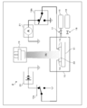
- thermo stimulation current measuring device 9 a sample stage 11 is provided inside the sample chamber 10.
- a temperature variable mechanism (not shown) for heating or cooling the semiconductor wafer 30 (sample) accommodated in the sample chamber 10 is incorporated in the outer wall portion of the sample chamber 10.
- the temperature of the sample chamber 10 and the temperature of the semiconductor wafer 30 accommodated in the sample chamber 10 are substantially the same temperature.
- the sample stage 11 supports the semiconductor wafer 30 to be measured.
- the light irradiation unit 13 irradiates the semiconductor wafer 30 accommodated in the sample chamber 10 with light having a specific wavelength. Specifically, the light irradiation unit 13 irradiates light having a wavelength having energy corresponding to the band gap of the semiconductor wafer 30.
- the sample chamber 10 is provided with two electrodes 14 and 14. These electrodes 14 and 14 are each electrically connected to the semiconductor wafer 30. As for the connection form of the electrodes 14 and 14 to the semiconductor wafer 30, the electrodes 14 and 14 are connected to different positions in the plane of the semiconductor wafer 30 as shown in the figure, so that they face each other with the semiconductor wafer 30 interposed therebetween. In some cases, the electrodes 14 may be disposed.
- a gas supply unit 15 and an exhaust unit 16 are connected to the sample chamber 10.
- the gas supply unit 15 supplies an inert gas to the sample chamber 10.
- the gas supply unit 15 supplies, for example, helium gas as an inert gas.
- a control valve 17 is provided in the middle of the pipe connecting the gas supply unit 15 and the sample chamber 10. The control valve 17 controls gas supply / stop by the gas supply unit 15, supply amount, and the like.
- the exhaust part 16 is for making the inside of the sample chamber 10 into a reduced pressure atmosphere (vacuum or the like).
- the exhaust unit 16 can be configured using, for example, a rotary pump.
- a control valve 18 is provided in the middle of the pipe connecting the exhaust unit 16 and the sample chamber 10. The control valve 18 controls the start and stop of exhaust by the exhaust unit 16 and the exhaust amount.
- One of the two electrodes 14, 14 described above is electrically connected to the voltage source 20 via the switch 19a.
- the other electrode 14 is electrically connected to the current measuring unit 21 via the switch 19b.
- the current measuring unit 21 is configured by using an ammeter capable of measuring a very small current of femtoampere (10 ⁇ 15 A).
- the temperature of the semiconductor wafer 30 in the sample chamber 10 is lowered from room temperature to a predetermined temperature Ts by a temperature variable mechanism (not shown).
- the predetermined temperature Ts described here is a temperature necessary for freezing the trap in the sample in the next second step.
- the switches 19a and 19b are switched from OFF to ON while the temperature of the semiconductor wafer 30 is maintained at the predetermined temperature Ts.
- a voltage necessary for generating excited carriers (hereinafter also referred to as “trapping voltage”) is applied from the voltage source 20 to the semiconductor wafer 30.
- the time tset for applying the trapping voltage is set (adjusted) in consideration of the time required to fill the trap with carriers.
- the semiconductor wafer 30 may be irradiated with light having a predetermined wavelength from the light irradiation unit 13 together with application of the trapping voltage.
- excited carriers (electrons, holes) are generated inside the semiconductor wafer 30, and the excited carriers are in a forbidden band Eg between the conduction band and the valence band. It is also called “trap level”). That is, electrons and holes generated by excitation are trapped in the donor level and the acceptor level, respectively.
- the trap level at which carriers are captured can be understood as the trap energy depth (hereinafter also referred to as “trap depth”). The amount of carriers captured in which trap level depends on the characteristics of the semiconductor wafer 30.
- the holding time tgset is set (adjusted) according to the time required to exclude surplus carriers other than the carriers to be captured in the trap from the forbidden band.
- a collecting voltage having a polarity opposite to that of the trapping voltage is applied to the semiconductor wafer 30 by the voltage source 20.
- the temperature of the semiconductor wafer 30 in the sample chamber 10 is raised at a constant speed by a temperature variable mechanism (not shown).
- the current measurement unit 21 measures the current (thermal stimulation current) that flows due to the release of carriers in the temperature rising process. The measurement of current in the temperature raising process ends when the temperature of the semiconductor wafer 30 reaches a predetermined temperature.
- mapping measurement In both the total reflection X-ray fluorescence analysis method and the thermally stimulated current measurement method, mapping measurement is applied. Hereinafter, the mapping measurement will be described in detail.
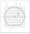
- the center of the semiconductor wafer 30 is defined as a coordinate center (0, 0), and is also referred to as an orthogonal coordinate (hereinafter referred to as an “XY coordinate”) defined by the X axis and the Y axis orthogonal to the coordinate center (origin). ) Is set.
- the X axis of the XY coordinates is a coordinate axis parallel to the orientation flat 31 of the semiconductor wafer.
- the surface area of the semiconductor wafer 30 is divided into a plurality of measurement positions using the above-described XY coordinates by designating the center of each measurement position with a coordinate value.
- the surface of the semiconductor wafer is divided into a plurality of measurement positions in a grid (or dot) arrangement.
- the size of one measurement position may be set in accordance with, for example, the X-ray spot size (for example, 10 mm ⁇ 10 mm) irradiated on the surface of the semiconductor wafer in the total reflection fluorescent X-ray analysis method.
- each measurement position can be uniquely specified by the coordinate values (x, y) of the XY coordinates.
- the surface of the semiconductor wafer is divided into a total of 100 measurement positions.
- the order of measurement can be arbitrarily set or changed.
- the measurement position specified by the coordinate values (x1, y1) is set as the measurement position to be measured for the first time
- the coordinate value ( The measurement position specified by x2, y1) is set as the measurement position to be measured for the second time.
- mapping measurement is performed in the following procedure in the measurement by the total reflection X-ray fluorescence analysis method.
- the stage 5 is moved by driving the stage moving mechanism unit 6 so that X-rays are irradiated to the measurement positions specified by the coordinate values (x1, y1) among the plurality of measurement positions.
- the measurement position is irradiated with X-rays, and measurement is performed by total reflection X-ray fluorescence analysis.
- measurement data D1txrf obtained by the total reflection X-ray fluorescence analysis method is obtained with respect to the measurement position designated by the coordinate value (x1, y1) (hereinafter also referred to as “measurement position (x1, y1)”).
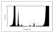
- the measurement data Dtxrf by total reflection X-ray fluorescence analysis can be represented by a graph of a TXRF spectrum in which the horizontal axis represents X-ray energy (wavelength) and the vertical axis represents X-ray intensity (see, for example, FIG. 6). ). From this measurement data Dtxrf, it is possible to know the type and amount of pollutant elements and the contamination state of the semiconductor wafer surface.
- the stage 5 is moved by driving the stage moving mechanism unit 6 so that X-rays are irradiated to the measurement position specified by the coordinate values (x2, y1).
- the measurement position is irradiated with X-rays, and measurement is performed by total reflection X-ray fluorescence analysis.
- measurement data D2txrf by the total reflection X-ray fluorescence analysis method is obtained with respect to the measurement position designated by the coordinate value (x2, y1) (hereinafter also referred to as “measurement position (x2, y1)”).
- the stage 5 is sequentially moved by driving the stage moving mechanism unit 6, and the remaining measurement positions are also measured by the total reflection X-ray fluorescence analysis method as described above.
- the measurement data Dtxrf and coordinate values (x, y) obtained by the total reflection X-ray fluorescence analysis method are obtained for all measurement positions.
- a total of 100 measurement results (hereinafter also referred to as “TXRF measurement results”) in association with the measurement positions designated by (hereinafter also referred to as “measurement positions (x, y)”) are obtained.
- mapping measurement is performed in the following procedure in the measurement by the thermally stimulated current measurement method.
- the thermally stimulated current measuring device includes, for example, a probing device (not shown) as means for realizing mapping measurement.
- a plurality of electrode pairs are formed on the surface of a semiconductor wafer as a sample corresponding to the plurality of measurement positions described above.
- One electrode pair is formed so as to sandwich the measurement position between one electrode and the other electrode within the surface of the semiconductor wafer in order to perform the thermal stimulation current measurement for one measurement position.
- a dummy (monitor) semiconductor wafer for sampling inspection (hereinafter also referred to as “dummy wafer”). May be introduced.
- the dummy wafer is basically subjected to the same processing (film formation processing etc.) as the product wafer. However, wirings and electrodes may be formed on the dummy wafer with a pattern different from that of the product wafer.
- a plurality of electrode pairs corresponding to a plurality of measurement positions are formed on the surface of the dummy wafer to be the semiconductor wafer 30 as described above, and thermally stimulated current measurement is performed using this dummy wafer.
- the stylus of the probing device is brought into contact with the electrode pair corresponding to the measurement position (x1, y1) among the plurality of electrode pairs, and the thermal stimulation current measurement is performed in that state. Thereby, the measurement data D1tsc of the thermal stimulation current is obtained for the measurement position (x1, y1).
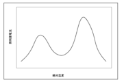
- the measurement data Dtsc obtained by the thermal stimulation current measurement method can be represented by a graph of a TSC spectrum in which the horizontal axis represents the absolute temperature and the vertical axis represents the thermal stimulation current (see, for example, FIG. 7). It is possible to know carrier trap depth and trap density, as well as electrical characteristics (characteristics such as charging, dielectric and insulation) of a semiconductor wafer.
- the probing apparatus and the semiconductor wafer are relatively moved by moving means (not shown).
- the stylus of the probing device is brought into contact with the electrode pair corresponding to the measurement position (x2, y1) different from the previous one, and the thermal stimulation current measurement is performed in that state.
- the measurement data D2tsc of the thermally stimulated current is obtained for the measurement position (x2, y1).
- the probing device and the semiconductor wafer are sequentially moved relative to each other by a moving means (not shown) to change the position of the electrode pair that contacts the stylus of the probing device.
- the remaining measurement positions are also measured by the thermally stimulated current measurement method as described above.
- the measurement data Dtsc and the measurement positions (x, y) by the thermally stimulated current measurement method are obtained for all measurement positions.
- a total of 100 measurement results associated with each other (hereinafter also referred to as “TSC measurement results”) are obtained.
- the thermally stimulated current may be measured by sandwiching the semiconductor wafer between two electrodes in the vertical direction (wafer thickness direction).
- the back surface (lower surface: the surface facing the sample stage) of the semiconductor wafer is used as a common electrode, and a plurality of electrodes corresponding to a plurality of measurement positions are formed on the front surface (upper surface) of the semiconductor wafer. deep.
- the probing apparatus and the semiconductor wafer (sample stage) are relatively moved to sequentially change the position of the electrode that contacts the stylus of the probing apparatus. Thereby, in the plane of the semiconductor wafer, the measurement data of the thermal stimulation current measurement is obtained for each measurement position with the position of the electrode brought into contact with the probe of the probing device as the measurement position.
- the sample measurement result processing apparatus 100 shown in the figure includes a computer apparatus including a central processing unit (CPU), a read-only memory (ROM), a random access memory (RAM), a hard disk drive, and the like, which are computer hardware resources.
- the input / output device pointing device, display device, printer device, etc. is used.
- the sample measurement result processing apparatus 100 functionally includes a first capturing unit 101, a second capturing unit 102, a storage unit 103, an integrating unit 104, a display unit 106, a display control unit 107, The input operation unit 108 and the main control unit 109 are provided.
- storage part 103 is comprised using memory devices, such as RAM and a hard-disk drive.
- the display unit 106 is configured using a display device.
- the input operation unit 108 is configured using a pointing device, a keyboard, and the like.
- each of the functional units of the first capturing unit 101, the second capturing unit 102, the integrating unit 104, the display control unit 107, and the main control unit 109 reads the program stored in the ROM into the RAM. It is realized by executing.
- a program for realizing these functional units is used by being installed in a computer device. Prior to the installation, a program stored in a storage medium (such as a CD-ROM) that can be read by the computer device is provided. Alternatively, it may be provided to the computer apparatus through a communication line connected to the computer apparatus. This program is an embodiment of the present invention.
- the first capturing unit 101 captures the measurement results in which the measurement data Dtxrf of the sample measured by the total reflection X-ray fluorescence analysis method and the measurement position (x, y) are associated with each of the measurement positions described above. It is.
- the second capturing unit 102 captures the measurement result in which the measurement data Dtsc of the sample measured by the thermal stimulation current measurement method and the measurement position (x, y) are associated with each of the measurement positions described above. .
- the storage unit 103 stores various data and information handled by the sample measurement result processing apparatus 100.
- the data and information stored in the storage unit 103 include the measurement result captured by the first capturing unit 101 and the measurement result captured by the second capturing unit 102.
- the integration unit 104 associates the measurement result acquired by the first acquisition unit 101 and the measurement result acquired by the second acquisition unit 102 with the measurement position (x, y) included in each measurement result. To be integrated.
- the display unit 106 displays various information as visible information to the user of the sample measurement result processing apparatus 100.
- the display unit 106 displays an image image of the surface of the semiconductor wafer 30 and displays the TXRF measurement result and the TSC measurement result associated with the measurement position with respect to one measurement position in the image image.
- the timing for displaying the TXRF measurement result and the TSC measurement result on the screen of the display unit 106 is not necessarily the same, but it is assumed that they are displayed together on the same screen at least for a certain period of time.
- the visible information displayed on the display unit 106 includes a distribution diagram of the contamination state of the sample surface reflecting the measurement result of the total reflection X-ray fluorescence analysis, and the user can arbitrarily input the distribution information using the input operation unit 108 in this distribution diagram. And a characteristic diagram showing the electrical characteristics of the sample reflecting the measurement result of the thermally stimulated current measurement method corresponding to the position designated in FIG.
- the display unit 106 is configured using, for example, a liquid crystal display device or an organic EL display device capable of color display.
- the display control unit 107 controls screen display by the display unit 106. Specifically, the display control unit 107 controls the display unit 106 to display information based on the image data by inputting image (drawing) data to the display unit 106. Further, the display control unit 107 controls to display the instructed information on the screen of the display unit 106 when an instruction is given from the user via the input operation unit 108. Switching of display information (characteristic chart and the like) to be described later is performed under the control of the display control unit 107.
- the input operation unit 108 is operated by a user who uses the sample measurement result processing apparatus 100 to input various information.
- the input operation unit 108 can be configured using a pointing device such as a mouse, a keyboard, and the like.
- the main control unit 109 controls the overall processing and operation of the sample measurement result processing apparatus 100.
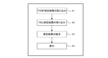
- FIG. 8 is a flowchart showing a sample measurement result processing method according to the embodiment of the present invention. Hereinafter, the processing contents of steps S1 to S4 will be described in order.
- the first capturing unit 101 measures the measurement data Dtxrf of the semiconductor wafer measured by the total reflection X-ray fluorescence analysis method and the measurement position ( The TXRF measurement result in which x, y) is associated is captured.
- the main control unit 109 stores the TXRF measurement result captured by the first capturing unit 101 in the storage unit 103.
- the acquisition of the TXRF measurement result may be performed by wired or wireless data communication (delivery) between the total reflection X-ray fluorescence analyzer and the sample measurement result processing apparatus 100.
- the TXRF measurement result may be captured by the following method.
- a portable recording medium for example, a USB memory
- the TXRF measurement result obtained by the total reflection X-ray fluorescence analysis method is recorded on the recording medium.
- the recording medium is removed from the total reflection fluorescent X-ray analyzer and connected to the input / output interface of the sample measurement result processing apparatus 100 or the like.
- the main control unit 109 reads out and captures the TXRF measurement result recorded on the recording medium, and stores the captured TXRF measurement result in the storage unit 103.
- TSC measurement result capture S2
- the second capturing unit 102 measures the measurement data Dtsc of the semiconductor wafer measured by the thermally stimulated current measurement method and the measurement position (x , Y) is captured.
- the main control unit 109 stores the TSC measurement result acquired by the second acquisition unit 102 in the storage unit 103.
- the acquisition of the TSC measurement result may be performed by the same method as the above-described acquisition of the TXRF measurement result. Further, the TSC measurement result may be captured before the TXRF measurement result is captured.
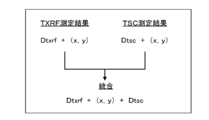
- the integration unit 104 uses the TXRF measurement result acquired by the first acquisition unit 101 and the TSC measurement result acquired by the second acquisition unit 102 as measurement positions (x, Associate and integrate by y). Specifically, as shown in FIG. 9, the TXRF measurement result in which the measurement data Dtxrf by the total reflection fluorescent X-ray analysis method and the measurement position (x, y) are associated with each other, and the measurement data Dtsc by the thermally stimulated current measurement method And the TSC measurement result associated with the measurement position (x, y) are linked by the measurement position (x, y) included in each measurement result, thereby integrating the TXRF measurement result and the TSC measurement result. To do.
- the TXRF measurement result and the TSC measurement result are stored in association with each other by the measurement position (x, y). For this reason, for example, when the user designates an arbitrary measurement position using the input operation unit 108, the measurement data Dtxrf and Dtsc associated with the designated measurement position (x, y) can be read from the storage unit 103. It becomes possible.
- FIG. 10 shows a specific display example.
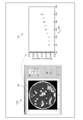
- a distribution map 120 showing the contamination state of the semiconductor wafer surface reflecting the TXRF measurement result is displayed in a mapping format.
- This distribution map 120 is displayed as one aspect of the TXRF measurement result.
- the types of elements (Cr, Mn, Fe, Ni in the illustrated example) of contaminants (contaminated metals) detected using total reflection X-ray fluorescence analysis are displayed in different colors. ing. Further, the amount (concentration) of contaminants present on the surface of the semiconductor wafer is displayed by contour lines.
- a characteristic diagram 121 showing the electrical characteristics of the semiconductor wafer reflecting the TSC measurement result corresponding to the measurement position Mp arbitrarily designated by the user in the distribution chart 120 is displayed in a graph format.
- the characteristic diagram 121 is displayed as one aspect of the TXRF measurement result.
- the measurement position Mp designated by the user in the distribution map 120 can be arbitrarily changed by, for example, moving the cursor to a desired position using a mouse and clicking the mouse there. Before the user actually designates the measurement position using the input operation unit 108, for example, the measurement position Mp having the largest amount of the contaminating element is automatically designated according to the default setting. Yes.
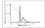
- the characteristic diagram 121 in the figure shows the electrical characteristics of the semiconductor wafer with the vertical axis representing the trap depth and the horizontal axis representing the absolute temperature.
- the graph data on which the characteristic diagram 121 is based is generated from the measurement data Dtsc obtained by the thermal stimulation current measurement method.
- a procedure for generating the graph data will be described.
- the partial temperature rising method is adopted as the temperature rising method in the thermally stimulated current measuring method, and the thermally stimulated current in the temperature rising process in each temperature range is measured.
- “temperature rise start” ⁇ “temperature rise stop” ⁇ “rapid cooling” is set as one cycle, and the temperature rise start temperature is sequentially shifted to the high temperature side, and this cycle is repeated multiple times. It is a warm method.
- I TSC ⁇ exp (-E / kT)
- E is an activation energy
- k is a Boltzmann constant
- T is an absolute temperature.
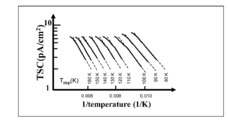
- the Arrhenius plot has the logarithm of thermally stimulated current density (pA / cm 2 ) on the vertical axis and the reciprocal (1 / T) of absolute temperature (K) on the horizontal axis.
- the slope of the Arrhenius plot in each temperature range is calculated from the above Arrhenius plot data group.
- the slope of the Arrhenius plot can be obtained, for example, by linear approximation using the least square method.
- the activation energy is obtained from the slope of the Arrhenius plot obtained as described above. Specifically, since the slope of the Arrhenius plot is represented by “ ⁇ E / k”, the activation energy “E” is obtained by multiplying this by the Boltzmann constant “k”. The activation energy is obtained for each temperature range. The activation energy thus obtained corresponds to energy indicating the carrier trap depth.
- graph data is generated in a form in which the slope of the Arrhenius plot obtained as described above is plotted on a graph showing the correlation between trap depth (activation energy) and absolute temperature.
- the graph data generated in this way is the graph data from which the characteristic diagram 121 is based.
- Each data processing described above may be performed by the thermally stimulated current measuring device or the sample measurement result processing device 100. Moreover, it may be distributed so that part of the data processing is performed by the thermally stimulated current measuring apparatus and the other data processing is performed by the sample measurement result processing apparatus 100.
- the electrical characteristic diagram displayed on the display unit 106 is not limited to the characteristic diagram 121 illustrated in FIG. 10, and may be, for example, the above-described FIG. 7 in which the measurement data Dtsc is graphed or the Arrhenius plot in FIG. 11.
- the number of carriers per unit volume / unit energy (cm ⁇ 3 eV ⁇ 1 ) or the number of carriers per unit area / unit energy (cm ⁇ ) is plotted on the vertical axis. 2 eV ⁇ 1 ), and a characteristic diagram graphed with activation energy (eV) on the horizontal axis.
- This characteristic diagram is obtained by integrating the number of carriers trapped at the trap depth for each trap depth using the graph data of the characteristic diagram 121 shown in FIG.
- the electrical characteristic diagram displayed on the display unit 106 may be configured to be changeable in accordance with a display switching instruction from the user using the input operation unit 108.
- a display switching instruction from the user using the input operation unit 108.
- the characteristic diagram 121 shown in FIG. 10 is displayed, and when the user gives a display switching instruction using the input operation unit 108 after that, the display control unit 107 receives the instruction to switch the display.
- the characteristic diagram displayed on the screen 106 may be changed to, for example, any one of the characteristic diagrams shown in FIGS.
- a TXRF spectrum chart 122 obtained when the measurement position Mp designated by the user is measured may be displayed.
- the TXRF spectrum chart 122 is displayed as one aspect of the TXRF measurement result.
- FIG. 13 instead of the distribution chart 120, an image as shown in FIG. 5 is displayed, and the TXRF measurement result (for example, the TXRF spectrum chart 122) associated with the measurement position designated in the image is displayed. ) And the TSC measurement result (any of the characteristic diagrams of FIGS. 10 to 12) may be displayed side by side.
- the type and amount of the contaminating element adhering to the surface of the semiconductor wafer 30 can be known, but it is not understood how it affects the electrical characteristics of the semiconductor wafer 30. Absent.
- the thermally stimulated current measurement method the electrical characteristics of the semiconductor wafer 30 can be understood, but it is not known what element caused it. According to the present embodiment, the lack of the total reflection X-ray fluorescence analysis method and the thermally stimulated current measurement method are mutually complemented, and the correlation between the contamination state of the sample surface and the electrical characteristics of the sample is grasped. Is possible.
- the contamination present at each measurement position Of the two measurement positions set on the surface of the semiconductor wafer 30, among the TXRF measurement results and the TSC measurement results integrated in association with each measurement position, according to the TXRF measurement result, the contamination present at each measurement position.
- the type and amount of the element can be known, and the electrical characteristics of the semiconductor wafer 30 at each measurement position can be understood from the TSC measurement results. In that case, it is assumed that the types of contaminating elements present at the respective measurement positions are the same and the amounts thereof are different. Then, a difference in the amount of contaminating elements appears as a difference in electrical characteristics of the semiconductor wafer 30 at each measurement position.
- the TXRF measurement result and the TSC measurement result are integrated and analyzed, so that even if the person is not an expert in process management, it is necessary to stop the process based on a certain criterion. It is possible to appropriately determine whether or not.
- the product yield can be improved compared to the case where the semiconductor manufacturing process is managed by setting independent criteria for the total reflection X-ray fluorescence analysis method and the thermally stimulated current measurement method. Can do.
- the reason for this is that even if the semiconductor wafer 30 is determined to be defective based on the measurement result of the total reflection X-ray fluorescence analysis method due to the application of the conventional determination criterion, the requirement is determined by the application of the new determination criterion according to the present embodiment. This is because there are more cases where products are finally commercialized as good products after satisfying quality. As a result, it is possible to improve the yield of semiconductor products and thus to achieve a significant cost reduction.
- the contamination level is, for example, 5 ⁇ 10 9 atoms / cm 2 .
- the peak temperature of the thermally stimulated current that appears in the temperature rising process varies from element to element, a peak may appear in a near temperature range depending on the element. Even in such a case, if the impurity element can be specified from the TXRF measurement result, an accurate conversion value can be obtained based on the element.
- FIG. 14 is a diagram showing a configuration example of a sample measurement result processing apparatus according to another embodiment of the present invention.
- the sample measurement result processing apparatus 100 shown in the drawing is different from the above-described embodiment in that a measurement position determination unit 105 is provided.
- the measurement position determination unit 105 determines the measurement position of the sample to be measured by the thermal stimulation current measurement method using the measurement result acquired by the first acquisition unit 101.
- the measurement position determination unit 105 is realized by the CPU reading the program stored in the ROM into the RAM and executing it.
- FIG. 15 is a flowchart showing a sample measurement result processing method according to the embodiment of the present invention. Hereinafter, the processing contents of steps S11 to S16 will be described in order.
- the first capturing unit 101 measures the measurement data Dtxrf of the semiconductor wafer measured by the total reflection X-ray fluorescence analysis method and the measurement position ( The TXRF measurement result in which x, y) is associated is captured.
- the main control unit 109 stores the TXRF measurement result captured by the first capturing unit 101 in the storage unit 103.
- the measurement position determination unit 105 determines the measurement position of the semiconductor wafer to be measured by the thermally stimulated current measurement method, using the TXRF measurement result taken in first. Specifically, for example, in the measurement data Dtxrf corresponding to each measurement position (x, y) obtained by the total reflection X-ray fluorescence analysis, the measurement in which the amount of contaminants exceeds a preset threshold value The position (x, y) is determined as the position to be measured by the thermally stimulated current measurement method.
- the threshold value may be set for quality determination of the semiconductor wafer 30 or may be set for semiconductor manufacturing process management. Further, the threshold value may be set so as to be commonly applied to all the polluting elements, or may be set for each type of polluting element.
- the main control unit 109 outputs the measurement position of the thermal stimulation current measurement method determined by the measurement position determination unit 105 earlier to the thermal stimulation current measuring device 9. Specifically, coordinate data indicating a measurement position to be measured by the thermal stimulation current measurement method is output to the thermal stimulation current measuring device 9 by, for example, wired or wireless communication. Thereby, in the thermally stimulated current measuring device 9 that has received the coordinate data output from the sample measurement result processing device 100, the thermally stimulated current of the semiconductor wafer is measured only for the measurement position indicated by the coordinate data.
- the second acquisition unit 102 actually measures the measurement positions (x, y) of the measurement positions (x, y) set on the surface of the semiconductor wafer by the thermally stimulated current measuring device 9.
- the TSC measurement result in which the measurement data Dtsc of the semiconductor wafer measured by the thermally stimulated current measurement method is associated with the measurement position (x, y) is captured.
- the TSC measurement result is captured only for the measurement position (x, y) determined by the measurement position determination unit 105.
- the main control unit 109 stores the TSC measurement result acquired by the second acquisition unit 102 in the storage unit 103.
- the integration unit 104 uses the TXRF measurement result acquired by the first acquisition unit 101 and the TSC measurement result acquired by the second acquisition unit 102 as measurement positions (x, Associate and integrate by y). In this case, the TSC measurement result is not stored in the storage unit 103 depending on the measurement position (x, y). Therefore, only the TSC measurement result stored in the storage unit 103 is integrated with the TXRF measurement result.
- the display control unit 107 displays predetermined information on the screen of the display unit 106 according to the display format set by default.
- the above-described integration of the TXRF measurement result and the TSC measurement result is performed only for those in which the TSC measurement result is stored in the storage unit 103. Therefore, the user is shown in the distribution diagram 120 shown on the left side of FIG. Depending on the measurement position Mp designated by, the characteristic diagram 121 may not be displayed on the right side of the figure.
- the measurement position of the semiconductor wafer 30 to be measured by the thermally stimulated current measurement method is determined and determined using the TXRF measurement result obtained by the total reflection X-ray fluorescence analysis method.
- the semiconductor wafer 30 is measured by the thermally stimulated current measurement method for only the measured position. For this reason, it is possible to shorten the measurement time and the data processing time as compared with the case where the measurement by the thermally stimulated current measurement method is performed on all measurement positions.
- the measurement position to be measured by the thermally stimulated current measurement method is determined based on the measurement result.
- the following procedure may be adopted.
- the measurement position to be measured by the total reflection X-ray fluorescence analysis method may be determined by performing measurement by the thermal stimulation current measurement method first and using the measurement result.
- the measurement position determination unit 105 determines the measurement position to be measured by the total reflection X-ray fluorescence analysis method using the TXRF measurement result by the total reflection X-ray fluorescence analyzer 1, and the coordinate data indicating the measurement position Is output to the total reflection fluorescent X-ray analyzer 1.
- the semiconductor wafer 30 used as a sample in each of the total reflection X-ray fluorescence analyzer 1 and the thermally stimulated current measuring device 9 may be extracted in the same process or a different process in a series of semiconductor manufacturing processes. May be good. Further, the sample is not limited to the substrate such as the semiconductor wafer 30, and any sample may be used as long as it has a flat surface (surface finished as a mirror surface) that can be measured by the total reflection X-ray fluorescence analysis.
- the total reflection X-ray fluorescence analyzer 1 and the thermally stimulated current measuring device 9 in which the sample measurement result processing device 100 takes in the measurement results are not limited to one each, and may be a plurality.
- the input operation unit 108 may be used by the user to arbitrarily select the display unit 106 to display the measurement result of the sample (semiconductor wafer) extracted in any process.
- the total reflection X-ray fluorescence analyzer 1 is installed in a certain process, and the thermal stimulation current measuring device 9 is installed in each of a plurality of different processes thereafter.
- One TXRF measurement result and TSC measurement results of a plurality of thermally stimulated current measuring devices 9 may be captured.
- the same coordinate system is used in both the total reflection X-ray fluorescence analysis method and the thermally stimulated current measurement method
- the measurement positions are divided by the same size
- the present invention is not limited to this.
- one of the total reflection fluorescent X-ray analysis method and the thermally stimulated current measurement method uses a rectangular coordinate (XY coordinate) to classify the measurement position
- the other method uses a polar coordinate to classify the measurement position. May be.
- the measurement position may be divided into different sizes by the total reflection X-ray fluorescence analysis method and the thermally stimulated current measurement method.
- the measurement position to be measured by the total reflection X-ray fluorescence analysis method and the measurement position to be measured by the thermal stimulation current measurement method are coordinate-transformed or the measurement positions are superimposed. It is necessary to correspond precisely.
- the pollutant to be measured by the total reflection X-ray fluorescence analysis method is not limited to metals, but may be organic substances, inorganic substances, natural oxides, and the like.
- the display form when the TXRF measurement result and the TSC measurement result are displayed together on the screen of the display unit 106 can be variously changed.
- each measurement result (measurement data) may be displayed in an overlapping manner.
- an analyzer that quantitatively analyzes the contaminating element based on the detection result of the detector 7 of the total reflection X-ray fluorescence analyzer 1 is provided in the total reflection X-ray fluorescence analyzer 1 or the sample measurement result processing device 100, and the user can
- the analysis result relating to the designated measurement position may be displayed on the screen of the display unit 106 as a specific numerical value.
- a third capturing unit that captures the inspection result of the foreign substance inspection apparatus may be provided. Then, a configuration may be adopted in which the foreign substance inspection result at the measurement position designated by the user in the image image on the surface of the semiconductor wafer is displayed on the screen of the display unit 106 with default settings or as necessary.
- DESCRIPTION OF SYMBOLS 1 Total reflection fluorescence X-ray analyzer 9 ... Thermally stimulated current measuring device 30 .
- Semiconductor wafer (sample) DESCRIPTION OF SYMBOLS 100 ...
- Sample measurement result processing apparatus 101 ... 1st acquisition part 102 . 2nd acquisition part 103 ... Memory
- storage part 104 ... Integration part 105 . Measurement position determination part 106 ... Display part 107 ... Display control part 108 ... Input operation part 109 ... Main control unit
Landscapes
- Physics & Mathematics (AREA)
- Health & Medical Sciences (AREA)
- Life Sciences & Earth Sciences (AREA)
- Chemical & Material Sciences (AREA)
- Analytical Chemistry (AREA)
- Biochemistry (AREA)
- General Health & Medical Sciences (AREA)
- General Physics & Mathematics (AREA)
- Immunology (AREA)
- Pathology (AREA)
- Analysing Materials By The Use Of Radiation (AREA)
- Investigating Or Analyzing Materials Using Thermal Means (AREA)
Abstract
本発明は、試料表面の汚染状態と試料の電気的特性の相関関係を把握することができる装置を提供することを目的とする。 本発明の試料測定結果処理装置(100)は、試料の表面を複数の測定位置に区分し、各々の測定位置に関して、全反射蛍光X線分析法により測定された試料の測定データと測定位置とを対応付けた第1の測定結果を取り込む第1の取り込み部(101)と、試料の表面を複数の測定位置に区分し、各々の測定位置に関して、熱刺激電流測定法により測定された試料の測定データと測定位置とを対応付けた第2の測定結果を取り込む第2の取り込み部(102)と、取り込まれた第1の測定結果と第2の測定結果とを、各々の測定結果に含まれる測定位置により関連付けて統合する統合部(104)と、を備える。試料の例は、半導体ウエハである。
Description
本発明は、試料測定結果処理装置、試料測定結果処理方法及びプログラムに関する。
従来、試料の測定(解析、分析等を含む)方法として、全反射蛍光X線分析法と熱刺激電流測定法が知られている。全反射蛍光X線分析法は、試料の表面に非常に浅い角度でX線を照射し、その際に汚染物の存在によって発生する蛍光X線を検出することにより、試料表面の汚染を測定する方法である(たとえば、特許文献1を参照)。熱刺激電流測定法は、試料に電界を加えることにより、試料内部や表面及び界面に存在する電荷トラップを注入キャリアで蓄積させ、昇温過程でのトラップサイトからの熱的放出(脱トラップ)現象で生じる熱刺激電流を測定する方法である(たとえば、特許文献2を参照)。熱刺激電流測定法に関しては、たとえば、JIS、K7131、電気学会技術報告書 第II部 第194号等にも規定されている。
一般に、半導体製造プロセスにおいては、特定のプロセスの評価や管理などに、全反射蛍光X線分析法や熱刺激電流測定法を利用している。たとえば、全反射蛍光X線分析法に関しては、半導体ウエハの表面の汚染状態に基づいて洗浄プロセスの評価あるいは管理などを行っている。また、熱刺激電流測定法に関しては、この測定方法によって得られる半導体ウエハの電気的特性に基づいて成膜プロセスの評価や管理などを行っている。
しかしながら、従来においては、全反射蛍光X線分析法を用いた半導体製造プロセスの評価等と、熱刺激電流測定法を用いた半導体製造プロセスの評価等を、それぞれ別々に行っている。このため、全反射蛍光X線分析法による測定では、半導体ウエハの表面の汚染状態は把握できても、この汚染状態が半導体ウエハの電気的特性にどのような影響を与えるのかは判断できなかった。また、熱刺激電流測定法による測定では、半導体ウエハの電気的特性は把握できても、実際に電気的特性に変化が生じた場合に、その原因がどのような欠陥(汚染など)によって引き起こされたのかは判断できなかった。
本発明の主な目的は、試料表面の汚染状態と試料の電気的特性の相関関係を把握することが可能な試料測定結果処理装置及び試料測定結果処理方法を提供することにある。
本発明の第1の態様は、
試料の表面を複数の測定位置に区分し、各々の測定位置に関して、全反射蛍光X線分析法により測定された前記試料の測定データと前記測定位置とを対応付けた第1の測定結果を取り込む第1の取り込み手段と、
前記試料の表面を複数の測定位置に区分し、各々の測定位置に関して、熱刺激電流測定法により測定された前記試料の測定データと前記測定位置とを対応付けた第2の測定結果を取り込む第2の取り込み手段と、
前記第1の取り込み手段によって取り込まれた前記第1の測定結果と前記第2の取り込み手段によって取り込まれた前記第2の測定結果とを、各々の測定結果に含まれる前記測定位置により関連付けて統合する統合手段と、
を備えることを特徴とする試料測定結果処理装置である。
試料の表面を複数の測定位置に区分し、各々の測定位置に関して、全反射蛍光X線分析法により測定された前記試料の測定データと前記測定位置とを対応付けた第1の測定結果を取り込む第1の取り込み手段と、
前記試料の表面を複数の測定位置に区分し、各々の測定位置に関して、熱刺激電流測定法により測定された前記試料の測定データと前記測定位置とを対応付けた第2の測定結果を取り込む第2の取り込み手段と、
前記第1の取り込み手段によって取り込まれた前記第1の測定結果と前記第2の取り込み手段によって取り込まれた前記第2の測定結果とを、各々の測定結果に含まれる前記測定位置により関連付けて統合する統合手段と、
を備えることを特徴とする試料測定結果処理装置である。
本発明の第2の態様は、
前記試料の表面のイメージ画像を表示するとともに、前記イメージ画像中の一つの測定位置に関して、当該測定位置により関連付けられた前記第1の測定結果と前記第2の測定結果を表示する表示手段をさらに備える
ことを特徴とする上記第1の態様に記載の試料測定結果処理装置である。
前記試料の表面のイメージ画像を表示するとともに、前記イメージ画像中の一つの測定位置に関して、当該測定位置により関連付けられた前記第1の測定結果と前記第2の測定結果を表示する表示手段をさらに備える
ことを特徴とする上記第1の態様に記載の試料測定結果処理装置である。
本発明の第3の態様は、
前記試料の表面のイメージ画像は、前記第1の測定結果を反映させた前記試料表面の汚染状態の分布図であり、
前記表示手段は、前記分布図でユーザーが任意に指定した測定位置に対応する前記第2の測定結果を反映させた前記試料の電気的特性を示す特性図を前記分布図と一緒に表示する
ことを特徴とする上記第2の態様に記載の試料測定結果処理装置である。
前記試料の表面のイメージ画像は、前記第1の測定結果を反映させた前記試料表面の汚染状態の分布図であり、
前記表示手段は、前記分布図でユーザーが任意に指定した測定位置に対応する前記第2の測定結果を反映させた前記試料の電気的特性を示す特性図を前記分布図と一緒に表示する
ことを特徴とする上記第2の態様に記載の試料測定結果処理装置である。
本発明の第4の態様は、
試料の表面を複数の測定位置に区分し、各々の測定位置に関して、全反射蛍光X線分析法及び熱刺激電流測定法のうち、一方の方法によって測定された前記試料の測定データと前記測定位置とを対応付けた第1の測定結果を取り込む第1の取り込みステップと、
前記全反射蛍光X線分析法及び前記熱刺激電流測定法のうち、他方の方法によって測定された前記試料の測定データと前記測定位置とを対応付けた第2の測定結果を取り込む第2の取り込みステップと、
前記第1の取り込みステップで取り込んだ前記第1の測定結果と前記第2の取り込みステップで取り込んだ前記第2の測定結果とを、各々の測定結果に含まれる前記測定位置により関連付けて統合する統合ステップと、
を備えることを特徴とする試料測定結果処理方法である。
試料の表面を複数の測定位置に区分し、各々の測定位置に関して、全反射蛍光X線分析法及び熱刺激電流測定法のうち、一方の方法によって測定された前記試料の測定データと前記測定位置とを対応付けた第1の測定結果を取り込む第1の取り込みステップと、
前記全反射蛍光X線分析法及び前記熱刺激電流測定法のうち、他方の方法によって測定された前記試料の測定データと前記測定位置とを対応付けた第2の測定結果を取り込む第2の取り込みステップと、
前記第1の取り込みステップで取り込んだ前記第1の測定結果と前記第2の取り込みステップで取り込んだ前記第2の測定結果とを、各々の測定結果に含まれる前記測定位置により関連付けて統合する統合ステップと、
を備えることを特徴とする試料測定結果処理方法である。
本発明の第5の態様は、
前記第1の取り込みステップで取り込まれた前記第1の測定結果を用いて、前記他方の方法によって測定すべき前記試料の測定位置を決定する位置決定ステップを含み、
前記第2の取り込みステップでは、前記位置決定ステップで決定された測定位置を対象に前記他方の方法によって前記試料を測定して得られた測定結果を取り込む
ことを特徴とする上記第4の態様に記載の試料測定結果処理方法である。
前記第1の取り込みステップで取り込まれた前記第1の測定結果を用いて、前記他方の方法によって測定すべき前記試料の測定位置を決定する位置決定ステップを含み、
前記第2の取り込みステップでは、前記位置決定ステップで決定された測定位置を対象に前記他方の方法によって前記試料を測定して得られた測定結果を取り込む
ことを特徴とする上記第4の態様に記載の試料測定結果処理方法である。
本発明の第6の態様は、
コンピュータを、
試料の表面を複数の測定位置に区分し、各々の測定位置に関して、全反射蛍光X線分析法により測定された前記試料の測定データと前記測定位置とを対応付けた第1の測定結果を取り込む第1の取り込み手段、
前記試料の表面を複数の測定位置に区分し、各々の測定位置に関して、熱刺激電流測定法により測定された前記試料の測定データと前記測定位置とを対応付けた第2の測定結果を取り込む第2の取り込み手段、
前記第1の取り込み手段によって取り込まれた前記第1の測定結果と前記第2の取り込み手段によって取り込まれた前記第2の測定結果とを、各々の測定結果に含まれる前記測定位置により関連付けて統合する統合手段、
として機能させることを特徴とするプログラムである。
コンピュータを、
試料の表面を複数の測定位置に区分し、各々の測定位置に関して、全反射蛍光X線分析法により測定された前記試料の測定データと前記測定位置とを対応付けた第1の測定結果を取り込む第1の取り込み手段、
前記試料の表面を複数の測定位置に区分し、各々の測定位置に関して、熱刺激電流測定法により測定された前記試料の測定データと前記測定位置とを対応付けた第2の測定結果を取り込む第2の取り込み手段、
前記第1の取り込み手段によって取り込まれた前記第1の測定結果と前記第2の取り込み手段によって取り込まれた前記第2の測定結果とを、各々の測定結果に含まれる前記測定位置により関連付けて統合する統合手段、
として機能させることを特徴とするプログラムである。
本発明によれば、試料表面の汚染状態と試料の電気的特性の相関関係を把握することが可能となる。
以下、本発明の実施の形態について図面を参照しつつ詳細に説明する。
本発明の実施の形態においては、次の順序で説明を行う。
1.全反射蛍光X線分析装置の構成
2.全反射蛍光X線分析法
3.熱刺激電流測定装置の構成
4.熱刺激電流測定法
5.試料測定結果処理装置の構成
6.試料測定結果処理方法
7.実施の形態の効果
8.他の実施の形態
9.他の実施の形態の効果
10.変形例等
本発明の実施の形態においては、次の順序で説明を行う。
1.全反射蛍光X線分析装置の構成
2.全反射蛍光X線分析法
3.熱刺激電流測定装置の構成
4.熱刺激電流測定法
5.試料測定結果処理装置の構成
6.試料測定結果処理方法
7.実施の形態の効果
8.他の実施の形態
9.他の実施の形態の効果
10.変形例等
図1は本発明の実施の形態に係る試料測定システムの構成例を示すブロック図である。図示した試料測定システムは、全反射蛍光X線分析装置1と、熱刺激電流測定装置9と、試料測定結果処理装置100と、を用いて構成されている。
本発明の実施の形態に係る試料測定結果処理装置及び試料測定結果処理方法は、全反射蛍光X線分析法(TRXF:Total Reflection X-ray Fluorescence)によって得られる測定結果と、熱刺激電流測定法(TSC:Thermally Stimulated Current)によって得られる測定結果とを取り込んで、所定の処理(詳細は後述)を行うものである。
ここでは、本発明の実施の形態に係る試料測定結果処理装置及び試料測定結果処理方法を説明する前に、全反射蛍光X線分析装置及び全反射蛍光X線分析法の説明と、熱刺激電流測定装置及び熱刺激電流測定方法の説明を順に行う。
ここでは、本発明の実施の形態に係る試料測定結果処理装置及び試料測定結果処理方法を説明する前に、全反射蛍光X線分析装置及び全反射蛍光X線分析法の説明と、熱刺激電流測定装置及び熱刺激電流測定方法の説明を順に行う。
<1.全反射蛍光X線分析装置の構成>
図2は全反射蛍光X線分析装置の構成例を示す概略図である。図示した全反射蛍光X線分析装置1は、試料表面の汚染を非破壊で測定する場合に用いられるものである。全反射蛍光X線分析装置1は、X線発生器2と、分光器3と、チャンバー4と、ステージ5と、ステージ移動機構部6と、検出器7と、を備えている。X線発生器2は、分光器3に向けてX線を出射するものである。X線発生器2は、たとえば、図示しないX線管と、回転陽極と、真空ポンプとを用いて構成される。また、X線発生器2には、必要に応じて、回転陽極を冷却する冷却器が設けられる。本発明の実施の形態においては、一例として、タングステンX線管を用いてX線発生器2が構成されているものとする。
図2は全反射蛍光X線分析装置の構成例を示す概略図である。図示した全反射蛍光X線分析装置1は、試料表面の汚染を非破壊で測定する場合に用いられるものである。全反射蛍光X線分析装置1は、X線発生器2と、分光器3と、チャンバー4と、ステージ5と、ステージ移動機構部6と、検出器7と、を備えている。X線発生器2は、分光器3に向けてX線を出射するものである。X線発生器2は、たとえば、図示しないX線管と、回転陽極と、真空ポンプとを用いて構成される。また、X線発生器2には、必要に応じて、回転陽極を冷却する冷却器が設けられる。本発明の実施の形態においては、一例として、タングステンX線管を用いてX線発生器2が構成されているものとする。
分光器3は、X線発生器2から出射されたX線を分光することにより、所定波長のX線をステージ5に導くものである。X線発生器2から分光器3に至る光路の途中には、図示しないシャッターが設けられている。シャッターは、光路上でX線の通過/遮断を切り替えるものである。分光器3からステージ5に至る光路の途中には、図示しないスリットが設けられている。スリットは、X線の通過する幅を制限するものである。
チャンバー4は、ステージ5やステージ移動機構部6を収容可能な大きさに形成されている。チャンバー4には、真空ポンプ8と図示しないガス供給系が接続されている。真空ポンプ8はチャンバー4内を真空状態にするためのものである。ガス供給系は、チャンバー4内に不活性ガスを供給するものである。
ステージ5は、試料を支持するものである。本実施の形態においては、一例として、半導体ウエハ(シリコンウエハ等)30を試料とし、この半導体ウエハ30をステージ5の上面に載せて支持するものとする。ステージ5は、半導体ウエハ30を静電チャック方式により固定状態に支持する。
ステージ移動機構部6は、マッピング測定を行うためにステージ5を移動させるものである。ここで記述する「マッピング測定」とは、試料の表面を複数の測定位置に区分し、各々の測定位置ごとに所定の測定を行うことをいう。マッピング測定を行うには、半導体ウエハ30の面内でX線の照射位置を変更する必要がある。そのため、ステージ移動機構部6は、半導体ウエハ30を支持するステージ5を直交二軸方向(X方向及びY方向)に移動させることにより、半導体ウエハ30に対するX線の照射位置を変更する。ステージ移動機構部6は、ステージ5をX方向及びY方向に移動可能なX-Yステージ、又はこれに回転移動を加えたX-Y-θステージを用いて構成することが可能である。加えて、ステージ移動機構部6は、ステージ5の高さを調整する高さ調整機構と、ステージ5の傾き(X線の入射角度)を調整する傾き調整機構と、を備えている。
検出器7は、ステージ5上に支持した半導体ウエハ30に所定の角度でX線を照射した際に発生する蛍光X線を検出するものである。ここで記述する所定の角度は、半導体ウエハ30の表面に入射したX線が全反射する角度である。検出器7は、たとえば、SSD(ソリッドステート検出器)、SDD(シリコンドリフト型検出器)などを用いて構成することが可能である。
<2.全反射蛍光X線分析法>
次に、上記構成から全反射蛍光X線分析装置1を用いた全反射蛍光X線分析法について説明する。
次に、上記構成から全反射蛍光X線分析装置1を用いた全反射蛍光X線分析法について説明する。
まず、チャンバー4内を不活性ガスで満たした真空空間とし、この真空空間内で半導体ウエハ30をステージ5により支持する。また、X線発生器2から出射したX線を分光器3で分光させることにより、所望の波長(エネルギー)のX線を半導体ウエハ30の表面に入射する。このとき、分光器3は、測定の対象とする汚染元素に適した波長のX線を取り出すべく、X線を単色化する。
半導体ウエハ30に入射するX線の波長は、測定(分析)すべき汚染元素に応じて分光器3により切り替える。たとえば、測定対象とする汚染物質が金属であれば、この汚染金属の元素が軽元素であるか、遷移元素であるか、それとも重元素であるかにより、分光器3で波長を切り替える。具体的には、X線発生器2にタングステンX線管を用いた場合は、汚染金属の元素が軽金属元素であればW-Mα線を照射し、遷移金属元素であればW-Lβ線を照射し、重金属元素であればH.E.(高エネルギー)線を照射するように、X線の波長を切り替える。
上述のように半導体ウエハ30の表面に所定波長のX線を照射すると、その照射位置に存在する汚染物質によって蛍光X線が発生する。このため、半導体ウエハ30の表面で発生する蛍光X線を検出器7で検出することにより、汚染元素の種類及び量を特定することができる。
さらに詳述すると、半導体ウエハ30に対しては、該ウエハ表面にX線を照射したときにX線が全反射するように、非常に浅い角度でX線を照射する。このため、半導体ウエハ30の表面に入射したX線は、汚染物質の存否にかかわらず、ほぼすべてが全反射する。よって、半導体ウエハ30に照射したX線が検出器7に検出されることはない。
これに対して、半導体ウエハ30の表面に汚染物質が存在し、この汚染物質にX線が照射されると、汚染物質の存在によって蛍光X線が放出される。蛍光X線は、半導体ウエハ30の表面で多方向に放射する。このため、放射する蛍光X線を検出器7で検出することができる。このとき、蛍光X線の波長は汚染元素の種類に依存し、蛍光X線の強度は汚染元素の量に依存したものとなる。このため、検出器7で検出した蛍光X線の波長を分析することにより、汚染物質を構成している汚染元素の種類及び量を特定することができる。
<3.熱刺激電流測定装置の構成>
次に、熱刺激電流測定装置の構成について図3を用いて説明する。
図示した熱刺激電流測定装置9においては、試料室10の内部に試料台11が設けられている。試料室10の外壁部分には、試料室10に収容した半導体ウエハ30(試料)を加熱したり冷却したりするための温度可変機構(不図示)が組み込まれている。本実施の形態においては、試料室10の温度と、試料室10に収容した半導体ウエハ30の温度とが、実質的に同じ温度であるとする。試料台11は、測定の対象となる半導体ウエハ30を支持するものである。
次に、熱刺激電流測定装置の構成について図3を用いて説明する。
図示した熱刺激電流測定装置9においては、試料室10の内部に試料台11が設けられている。試料室10の外壁部分には、試料室10に収容した半導体ウエハ30(試料)を加熱したり冷却したりするための温度可変機構(不図示)が組み込まれている。本実施の形態においては、試料室10の温度と、試料室10に収容した半導体ウエハ30の温度とが、実質的に同じ温度であるとする。試料台11は、測定の対象となる半導体ウエハ30を支持するものである。
光照射部13は、試料室10に収容された半導体ウエハ30に対して、特定波長の光を照射するものである。具体的には、光照射部13は、半導体ウエハ30のバンドギャップに相当するエネルギーをもつ波長の光を照射する。
試料室10には、2つの電極14,14が設けられている。これらの電極14,14は、それぞれ半導体ウエハ30に電気的に接続されるものである。半導体ウエハ30に対する電極14,14の接続形態としては、図例のように半導体ウエハ30の面内で異なる位置に電極14,14を接続する以外にも、半導体ウエハ30を挟んで対向するように電極14,14を配置する場合もある。
試料室10には、ガス供給部15と排気部16とが接続されている。ガス供給部15は、試料室10に不活性ガスを供給するものである。ガス供給部15は、不活性ガスとして、たとえばヘリウムガスを供給する。ガス供給部15と試料室10をつなぐ配管の途中には制御弁17が設けられている。制御弁17は、ガス供給部15によるガスの供給や停止、供給量などを制御するものである。
排気部16は、試料室10の内部を減圧雰囲気(真空等)にするためものである。排気部16は、たとえば、ロータリーポンプを用いて構成することが可能である。排気部16と試料室10とをつなぐ配管の途中には制御弁18が設けられている。制御弁18は、排気部16による排気の開始や停止、排気量などを制御するものである。
上述した2つの電極14,14のうち、一方の電極14は、スイッチ19aを介して電圧源20に電気的に接続されている。他方の電極14は、スイッチ19bを介して電流計測部21に電気的に接続されている。電流計測部21は、フェムトアンペア(10-15A)という非常に微小な電流を測定可能な電流計を用いて構成される。
<4.熱刺激電流測定法>
次に、上記構成から熱刺激電流測定装置を用いた熱刺激電流測定法について図4を参照しながら説明する。
次に、上記構成から熱刺激電流測定装置を用いた熱刺激電流測定法について図4を参照しながら説明する。
まず、試料室10の試料台11に半導体ウエハ30をセットして電極14,14を接続した後、ガス供給部15及び排気部16により、試料室10の内部を不活性ガスで満たした減圧雰囲気にする。また、第1ステップでは、図示しない温度可変機構により試料室10内の半導体ウエハ30の温度を室温から所定の温度Tsまで低下させる。ここで記述する所定の温度Tsとは、次の第2ステップにおいて、試料内のトラップを凍結させるのに必要な温度である。
次に、半導体ウエハ30の温度を所定の温度Tsに維持した状態で、スイッチ19a,19bをオフからオンに切り替える。これにより、励起キャリアの発生に必要な電圧(以下、「トラッピング電圧」ともいう。)が、電圧源20から半導体ウエハ30に印加される。トラッピング電圧を印加する時間tsetは、トラップをキャリアで満たすのに必要な時間を考慮して設定(調整)される。このとき、必要に応じて、トラッピング電圧の印加とあわせて、光照射部13から半導体ウエハ30に所定波長の光を照射してもよい。これにより、半導体ウエハ30の内部では、励起キャリア(電子、正孔)が発生するとともに、この励起キャリアが、伝導帯と価電子帯との間の禁制帯Egにおいて、あるエネルギー準位(以下、「トラップ準位」ともいう。)に捕獲される。すなわち、励起によって発生した電子と正孔は、それぞれドナー準位とアクセプター準位に捕獲される。このとき、キャリアが捕獲されるトラップ準位は、トラップエネルギーの深さ(以下、「トラップ深さ」ともいう。)として捉えることができる。いずれのトラップ準位に、どの程度の量のキャリアが捕獲されるかは、半導体ウエハ30の特性によって異なる。
次に、スイッチ19a,19bをオンからオフに切り替えることにより、トラッピング電圧の印加を停止し、この状態をあらかじめ設定された保持時間tgsetだけ保持する。保持時間tgsetは、トラップに捕獲すべきキャリア以外の余剰キャリアを禁制帯から排除するのに必要な時間に応じて設定(調整)される。
次に、スイッチ19a,91bをオフからオンに切り替えることにより、トラッピング電圧と逆極性のコレクティング電圧を電圧源20によって半導体ウエハ30に印加する。また、それと同時に、試料室10内の半導体ウエハ30を図示しない温度可変機構により一定速度で昇温させる。そして、この昇温過程でキャリアの解放により流れる電流(熱刺激電流)を電流計測部21で測定する。この昇温過程における電流の測定は、半導体ウエハ30の温度があらかじめ決められた温度に達した段階で終了する。
(マッピング測定)
上述した全反射蛍光X線分析法及び熱刺激電流測定法においては、いずれもマッピング測定を適用する。以下、マッピング測定について詳しく説明する。
マッピング測定においては、図5に示すように、試料となる半導体ウエハ30の表面に二次元の座標を設定する。具体的には、半導体ウエハ30の中心を座標中心(0,0)とし、この座標中心(原点)で直交するX軸とY軸により規定される直交座標(以下、「XY座標」ともいう。)を設定する。XY座標のX軸は、半導体ウエハのオリエンテーションフラット31と平行な座標軸とする。
上述した全反射蛍光X線分析法及び熱刺激電流測定法においては、いずれもマッピング測定を適用する。以下、マッピング測定について詳しく説明する。
マッピング測定においては、図5に示すように、試料となる半導体ウエハ30の表面に二次元の座標を設定する。具体的には、半導体ウエハ30の中心を座標中心(0,0)とし、この座標中心(原点)で直交するX軸とY軸により規定される直交座標(以下、「XY座標」ともいう。)を設定する。XY座標のX軸は、半導体ウエハのオリエンテーションフラット31と平行な座標軸とする。
また、マッピング測定においては、各々の測定位置の中心を座標値で指定することにより、半導体ウエハ30の表面領域を上述したXY座標を用いて複数の測定位置に区分する。具体的には、半導体ウエハの表面を格子状(又はドット状)の配列で複数の測定位置に区分する。一つの測定位置の大きさは、たとえば、全反射蛍光X線分析法において半導体ウエハの表面に照射されるX線のスポットサイズ(たとえば、10mm×10mm)にあわせて設定すればよい。これにより、半導体ウエハ30の面内において、各々の測定位置をXY座標の座標値(x,y)で一義的に特定することが可能となる。
本実施の形態においては、半導体ウエハの表面を合計100個の測定位置に区分するものと仮定する。また、測定する順番は、任意に設定又は変更が可能であるが、ここでは一例として、座標値(x1,y1)で指定される測定位置を1回目に測定すべき測定位置とし、座標値(x2,y1)で指定される測定位置を2回目に測定すべき測定位置とする。
本実施の形態においては、半導体ウエハの表面を合計100個の測定位置に区分するものと仮定する。また、測定する順番は、任意に設定又は変更が可能であるが、ここでは一例として、座標値(x1,y1)で指定される測定位置を1回目に測定すべき測定位置とし、座標値(x2,y1)で指定される測定位置を2回目に測定すべき測定位置とする。
上述のように半導体ウエハの表面を複数の測定位置に区分した場合、全反射蛍光X線分析法による測定では、次のような手順でマッピング測定を行う。
まず、ステージ移動機構部6の駆動により、複数の測定位置のうち、座標値(x1,y1)で指定される測定位置にX線が照射されるように、ステージ5を移動させる。
次に、その測定位置にX線を照射して、全反射蛍光X線分析法による測定を行う。これにより、座標値(x1,y1)で指定される測定位置(以下、「測定位置(x1,y1)」とも記す。)に関して、全反射蛍光X線分析法による測定データD1txrfが得られる。
全反射蛍光X線分析法による測定データDtxrfは、横軸にX線のエネルギー(波長)、縦軸にX線の強度をとったTXRFスペクトルのグラフで表すことができる(たとえば、図6を参照)。この測定データDtxrfからは、汚染物質の元素の種類や量、さらには半導体ウエハ表面の汚染状態を知ることができる。
まず、ステージ移動機構部6の駆動により、複数の測定位置のうち、座標値(x1,y1)で指定される測定位置にX線が照射されるように、ステージ5を移動させる。
次に、その測定位置にX線を照射して、全反射蛍光X線分析法による測定を行う。これにより、座標値(x1,y1)で指定される測定位置(以下、「測定位置(x1,y1)」とも記す。)に関して、全反射蛍光X線分析法による測定データD1txrfが得られる。
全反射蛍光X線分析法による測定データDtxrfは、横軸にX線のエネルギー(波長)、縦軸にX線の強度をとったTXRFスペクトルのグラフで表すことができる(たとえば、図6を参照)。この測定データDtxrfからは、汚染物質の元素の種類や量、さらには半導体ウエハ表面の汚染状態を知ることができる。
次に、ステージ移動機構部6の駆動により、座標値(x2,y1)で指定される測定位置にX線が照射されるように、ステージ5を移動させる。
次に、その測定位置にX線を照射して、全反射蛍光X線分析法による測定を行う。これにより、座標値(x2,y1)で指定される測定位置(以下、「測定位置(x2,y1)」とも記す。)に関して、全反射蛍光X線分析法による測定データD2txrfが得られる。
次に、その測定位置にX線を照射して、全反射蛍光X線分析法による測定を行う。これにより、座標値(x2,y1)で指定される測定位置(以下、「測定位置(x2,y1)」とも記す。)に関して、全反射蛍光X線分析法による測定データD2txrfが得られる。
以降は、ステージ移動機構部6の駆動によりステージ5を順次移動させ、残りの測定位置に関しても、上記同様に全反射蛍光X線分析法による測定を行う。これにより、上述のように半導体ウエハの表面を合計100個の測定位置に区分したと仮定すると、すべての測定位置に関して、全反射蛍光X線分析法による測定データDtxrfと座標値(x,y)で指定される測定位置(以下、「測定位置(x,y)」とも記す。)とを対応付けた合計100個の測定結果(以下、「TXRF測定結果」ともいう。)が得られる。
また、上述のように半導体ウエハの表面を複数の測定位置に区分した場合、熱刺激電流測定法による測定では、次のような手順でマッピング測定を行う。
まず、説明の前提として、熱刺激電流測定装置は、マッピング測定を実現するための手段として、たとえば、図示しないプロービング装置を備えるものとする。また、試料となる半導体ウエハの表面には、上述した複数の測定位置に対応して複数の電極対が形成されているものとする。一つの電極対は、一つの測定位置を対象に熱刺激電流測定を行うために、半導体ウエハの面内において当該測定位置を一方の電極と他方の電極で挟むように形成されるものである。
まず、説明の前提として、熱刺激電流測定装置は、マッピング測定を実現するための手段として、たとえば、図示しないプロービング装置を備えるものとする。また、試料となる半導体ウエハの表面には、上述した複数の測定位置に対応して複数の電極対が形成されているものとする。一つの電極対は、一つの測定位置を対象に熱刺激電流測定を行うために、半導体ウエハの面内において当該測定位置を一方の電極と他方の電極で挟むように形成されるものである。
半導体製造プロセスにおいては、製品として取り扱う半導体ウエハ(以下、「製品ウエハ」ともいう。)の他に、抜き取り検査のためのダミー(モニター用)の半導体ウエハ(以下、「ダミーウエハ」ともいう。)を導入する場合がある。ダミーウエハには基本的に製品ウエハと同様の処理(成膜処理など)が施される。ただし、ダミーウエハには、製品ウエハとは異なるパターンで配線や電極を形成することがある。
そこで、半導体ウエハ30となるダミーウエハの表面に、上述のように複数の測定位置に対応して複数の電極対を形成し、このダミーウエハを使って熱刺激電流測定を行う。その場合は、まず、複数の電極対のうち、測定位置(x1,y1)に対応する電極対にプロービング装置の触針を接触させ、その状態で熱刺激電流測定を行う。これにより、測定位置(x1,y1)に関して、熱刺激電流の測定データD1tscが得られる。熱刺激電流測定法による測定データDtscは、横軸に絶対温度、縦軸に熱刺激電流をとったTSCスペクトルのグラフで表すことができる(たとえば、図7を参照)この測定データDtscからは、キャリアのトラップ深さやトラップ密度、さらには半導体ウエハの電気的特性(帯電、誘電、絶縁などの特性)を知ることができる。
次に、プロービング装置を半導体ウエハから離間させた後、図示しない移動手段によりプロービング装置と半導体ウエハ(試料台)を相対的に移動させる。次いで、プロービング装置を半導体ウエハに接近させることにより、先ほどと異なる測定位置(x2,y1)に対応する電極対にプロービング装置の触針を接触させ、その状態で熱刺激電流測定を行う。これにより、測定位置(x2,y1)に関して、熱刺激電流の測定データD2tscが得られる。
以降は、プロービング装置と半導体ウエハ(試料台)を図示しない移動手段により順次、相対的に移動させて、プロービング装置の触針を接触させる電極対の位置を変更する。そして、残りの測定位置に関しても、上記同様に熱刺激電流測定法による測定を行う。これにより、上述のように半導体ウエハの表面を合計100個の測定位置に区分したと仮定すると、すべての測定位置に関して、熱刺激電流測定法による測定データDtscと測定位置(x、y)とを対応付けた合計100個の測定結果(以下、「TSC測定結果」ともいう。)が得られる。
なお、熱刺激電流測定法においては、半導体ウエハを上下方向(ウエハ厚み方向)で2つの電極により挟んで熱刺激電流測定を行う場合がある。その場合は、たとえば、半導体ウエハの裏面(下面:試料台と対面する側の面)を共通の電極とし、半導体ウエハの表面(上面)に複数の測定位置に対応する複数の電極を形成しておく。そして、上記同様にプロービング装置と半導体ウエハ(試料台)を相対的に移動させて、プロービング装置の触針を接触させる電極の位置を順に変更する。これにより、半導体ウエハの面内において、プロービング装置の触針を接触させた電極の位置をそれぞれ測定位置として、測定位置ごとに熱刺激電流測定の測定データが得られる。
<5.試料測定結果処理装置の構成>
次に、本発明の実施の形態に係る試料測定結果処理装置について図1を参照しつつ説明する。図示した試料測定結果処理装置100は、コンピュータハードウェア資源であるCPU(central processing unit)、ROM(Read-Only Memory)、RAM(Random Access Memory)、ハードディスクドライブなどを備えるコンピュータ装置と、これに付属する入出力用のデバイス(ポインティングデバイス等、ディスプレイ装置、プリンタ装置など)を用いて構成されるものである。
次に、本発明の実施の形態に係る試料測定結果処理装置について図1を参照しつつ説明する。図示した試料測定結果処理装置100は、コンピュータハードウェア資源であるCPU(central processing unit)、ROM(Read-Only Memory)、RAM(Random Access Memory)、ハードディスクドライブなどを備えるコンピュータ装置と、これに付属する入出力用のデバイス(ポインティングデバイス等、ディスプレイ装置、プリンタ装置など)を用いて構成されるものである。
試料測定結果処理装置100は、機能的には、第1の取り込み部101と、第2の取り込み部102と、記憶部103と、統合部104と、表示部106と、表示制御部107と、入力操作部108と、主制御部109と、を備えた構成になっている。このうち、記憶部103は、RAMやハードディスクドライブなどのメモリ装置を用いて構成される。表示部106は、ディスプレイ装置を用いて構成される。入力操作部108は、ポインティングデバイス、キーボードなどを用いて構成される。
これに対して、第1の取り込み部101、第2の取り込み部102、統合部104、表示制御部107、主制御部109の各機能部は、CPUがROMに記憶されたプログラムをRAMに読み出して実行することにより実現される。これらの機能部を実現するためのプログラムは、コンピュータ装置にインストールされて用いられるが、そのインストールに先立ち、コンピュータ装置で読み取り可能な記憶媒体(CD-ROMなど)に格納されて提供されるものであってもよいし、あるいはコンピュータ装置と接続する通信回線を通じてコンピュータ装置に提供されるものであってもよい。このプログラムは、本発明の一形態となる。
(第1の取り込み部)
第1の取り込み部101は、上述した各々の測定位置に関して、全反射蛍光X線分析法により測定された試料の測定データDtxrfと測定位置(x,y)とを対応付けた測定結果を取り込むものである。
第1の取り込み部101は、上述した各々の測定位置に関して、全反射蛍光X線分析法により測定された試料の測定データDtxrfと測定位置(x,y)とを対応付けた測定結果を取り込むものである。
(第2の取り込み部)
第2の取り込み部102は、上述した各々の測定位置に関して、熱刺激電流測定法により測定された試料の測定データDtscと測定位置(x,y)とを対応付けた測定結果を取り込むものである。
第2の取り込み部102は、上述した各々の測定位置に関して、熱刺激電流測定法により測定された試料の測定データDtscと測定位置(x,y)とを対応付けた測定結果を取り込むものである。
(記憶部)
記憶部103は、試料測定結果処理装置100で取り扱う種々のデータや情報を記憶するものである。記憶部103に記憶されるデータや情報には、第1の取り込み部101によって取り込まれた測定結果と、第2の取り込み部102によって取り込まれた測定結果とが含まれる。
記憶部103は、試料測定結果処理装置100で取り扱う種々のデータや情報を記憶するものである。記憶部103に記憶されるデータや情報には、第1の取り込み部101によって取り込まれた測定結果と、第2の取り込み部102によって取り込まれた測定結果とが含まれる。
(統合部)
統合部104は、第1の取り込み部101によって取り込まれた測定結果と第2の取り込み部102によって取り込まれた測定結果とを、各々の測定結果に含まれる測定位置(x、y)により関連付けて統合するものである。
統合部104は、第1の取り込み部101によって取り込まれた測定結果と第2の取り込み部102によって取り込まれた測定結果とを、各々の測定結果に含まれる測定位置(x、y)により関連付けて統合するものである。
(表示部)
表示部106は、試料測定結果処理装置100のユーザーに対して各種の情報を可視情報として表示するものである。表示部106は、半導体ウエハ30の表面のイメージ画像を表示するとともに、このイメージ画像中の一つの測定位置に関して、当該測定位置により関連付けられたTXRF測定結果とTSC測定結果を表示する。表示部106の画面にTXRF測定結果とTSC測定結果を表示するタイミングは、必ずしも同時でなくてもよいが、少なくとも或る時間においては同一画面上に一緒に表示されるものとする。表示部106に表示される可視情報には、全反射蛍光X線分析法の測定結果を反映させた試料表面の汚染状態の分布図と、この分布図でユーザーが入力操作部108を用いて任意に指定した位置に対応する熱刺激電流測定法の測定結果を反映させた試料の電気的特性を示す特性図とが含まれる。表示部106は、たとえば、カラー表示が可能な液晶表示装置や有機EL表示装置などを用いて構成される。
表示部106は、試料測定結果処理装置100のユーザーに対して各種の情報を可視情報として表示するものである。表示部106は、半導体ウエハ30の表面のイメージ画像を表示するとともに、このイメージ画像中の一つの測定位置に関して、当該測定位置により関連付けられたTXRF測定結果とTSC測定結果を表示する。表示部106の画面にTXRF測定結果とTSC測定結果を表示するタイミングは、必ずしも同時でなくてもよいが、少なくとも或る時間においては同一画面上に一緒に表示されるものとする。表示部106に表示される可視情報には、全反射蛍光X線分析法の測定結果を反映させた試料表面の汚染状態の分布図と、この分布図でユーザーが入力操作部108を用いて任意に指定した位置に対応する熱刺激電流測定法の測定結果を反映させた試料の電気的特性を示す特性図とが含まれる。表示部106は、たとえば、カラー表示が可能な液晶表示装置や有機EL表示装置などを用いて構成される。
(表示制御部)
表示制御部107は、表示部106による画面表示を制御するものである。具体的には、表示制御部107は、表示部106に画像(描画)データを入力することにより、その画像データに基づく情報を表示部106の画面に表示するように制御する。また、表示制御部107は、入力操作部108を介してユーザーから何らかの指示がされた場合に、指示された情報を表示部106の画面に表示するように制御する。後述する表示情報(特性図等)の切り替えは、この表示制御部107による制御のもとで行われる。
表示制御部107は、表示部106による画面表示を制御するものである。具体的には、表示制御部107は、表示部106に画像(描画)データを入力することにより、その画像データに基づく情報を表示部106の画面に表示するように制御する。また、表示制御部107は、入力操作部108を介してユーザーから何らかの指示がされた場合に、指示された情報を表示部106の画面に表示するように制御する。後述する表示情報(特性図等)の切り替えは、この表示制御部107による制御のもとで行われる。
(入力操作部)
入力操作部108は、試料測定結果処理装置100を使用するユーザーが種々の情報を入力するために操作するものである。入力操作部108は、マウス等のポインティングデバイス、キーボードなどを用いて構成することが可能である。
入力操作部108は、試料測定結果処理装置100を使用するユーザーが種々の情報を入力するために操作するものである。入力操作部108は、マウス等のポインティングデバイス、キーボードなどを用いて構成することが可能である。
(主制御部)
主制御部109は、試料測定結果処理装置100全体の処理、動作を統括的に制御するものである。
主制御部109は、試料測定結果処理装置100全体の処理、動作を統括的に制御するものである。
<試料測定結果処理方法>
図8は本発明の実施の形態に係る試料測定結果処理方法を示すフローチャートである。以下、各ステップS1~S4の処理内容について順に説明する。
図8は本発明の実施の形態に係る試料測定結果処理方法を示すフローチャートである。以下、各ステップS1~S4の処理内容について順に説明する。
(TXRF測定結果の取り込み:S1)
まず、第1の取り込み部101は、半導体ウエハの表面に設定された各々の測定位置(x,y)に関して、全反射蛍光X線分析法によって測定された半導体ウエハの測定データDtxrfと測定位置(x,y)とを対応付けたTXRF測定結果を取り込む。このとき、主制御部109は、第1の取り込み部101が取り込んだTXRF測定結果を記憶部103に記憶する。TXRF測定結果の取り込みは、全反射蛍光X線分析装置と試料測定結果処理装置100との間で有線又は無線によるデータの通信(受け渡し)によって行えばよい。
まず、第1の取り込み部101は、半導体ウエハの表面に設定された各々の測定位置(x,y)に関して、全反射蛍光X線分析法によって測定された半導体ウエハの測定データDtxrfと測定位置(x,y)とを対応付けたTXRF測定結果を取り込む。このとき、主制御部109は、第1の取り込み部101が取り込んだTXRF測定結果を記憶部103に記憶する。TXRF測定結果の取り込みは、全反射蛍光X線分析装置と試料測定結果処理装置100との間で有線又は無線によるデータの通信(受け渡し)によって行えばよい。
ただし、本発明はこれに限らず、たとえば、次のような方法でTXRF測定結果の取り込みを行ってもよい。まず、全反射蛍光X線分析装置の入出力インターフェース等に携帯型の記録媒体(たとえば、USBメモリ等)を接続し、全反射蛍光X線分析法によって得られたTXRF測定結果を記録媒体に記録する。次に、この記録媒体を全反射蛍光X線分析装置から取り外して、試料測定結果処理装置100の入出力インターフェース等に接続する。次に、試料測定結果処理装置100において、記録媒体に記録されているTXRF測定結果を主制御部109が読み出して取り込むとともに、取り込んだTXRF測定結果を記憶部103に記憶する。
(TSC測定結果の取り込み:S2)
次に、第2の取り込み部102は、半導体ウエハの表面に設定された各々の測定位置(x,y)に関して、熱刺激電流測定法によって測定された半導体ウエハの測定データDtscと測定位置(x,y)とを対応付けたTSC測定結果を取り込む。このとき、主制御部109は、第2の取り込み部102が取り込んだTSC測定結果を記憶部103に記憶する。TSC測定結果の取り込みは、上述したTXRF測定結果の取り込みと同様の方法で行えばよい。また、TSC測定結果の取り込みは、TXRF測定結果の取り込みよりも前に行ってもよい。
次に、第2の取り込み部102は、半導体ウエハの表面に設定された各々の測定位置(x,y)に関して、熱刺激電流測定法によって測定された半導体ウエハの測定データDtscと測定位置(x,y)とを対応付けたTSC測定結果を取り込む。このとき、主制御部109は、第2の取り込み部102が取り込んだTSC測定結果を記憶部103に記憶する。TSC測定結果の取り込みは、上述したTXRF測定結果の取り込みと同様の方法で行えばよい。また、TSC測定結果の取り込みは、TXRF測定結果の取り込みよりも前に行ってもよい。
(測定結果の統合:S3)
次に、統合部104は、第1の取り込み部101によって取り込まれたTXRF測定結果と第2の取り込み部102によって取り込まれたTSC測定結果とを、各々の測定結果に含まれる測定位置(x,y)により関連付けて統合する。具体的には、図9に示すように、全反射蛍光X線分析法による測定データDtxrfと測定位置(x,y)とを対応付けたTXRF測定結果と、熱刺激電流測定法による測定データDtscと測定位置(x,y)とを対応付けたTSC測定結果とを、それぞれの測定結果に含まれる測定位置(x,y)によって紐付けすることにより、TXRF測定結果とTSC測定結果とを統合する。
次に、統合部104は、第1の取り込み部101によって取り込まれたTXRF測定結果と第2の取り込み部102によって取り込まれたTSC測定結果とを、各々の測定結果に含まれる測定位置(x,y)により関連付けて統合する。具体的には、図9に示すように、全反射蛍光X線分析法による測定データDtxrfと測定位置(x,y)とを対応付けたTXRF測定結果と、熱刺激電流測定法による測定データDtscと測定位置(x,y)とを対応付けたTSC測定結果とを、それぞれの測定結果に含まれる測定位置(x,y)によって紐付けすることにより、TXRF測定結果とTSC測定結果とを統合する。
このような処理を行うことにより、記憶部103においては、TXRF測定結果とTSC測定結果とが測定位置(x,y)により関連付けて保存される。このため、たとえばユーザーが入力操作部108を用いて任意の測定位置を指定した場合は、指定の測定位置(x,y)によって関連付けられている測定データDtxrf、Dtscを記憶部103から読み出すことが可能となる。
(表示:S4)
次に、表示制御部107は、デフォルトで設定されている表示形式にしたがって表示部106の画面に所定の情報を表示させる。図10に具体的な表示例を示す。
図10においては、半導体ウエハ30の表面のイメージ画像として、TXRF測定結果を反映させた半導体ウエハ表面の汚染状態を示す分布図120がマッピング形式で表示されている。この分布図120は、TXRF測定結果の一態様として表示されたものである。図示した分布図120においては、全反射蛍光X線分析法を用いて検出された汚染物質(汚染金属)の元素の種類(図例ではCr、Mn、Fe、Ni)がそれぞれ異なる色で表示されている。また、半導体ウエハ表面に存在する汚染物質の量(濃度)が等高線で表示されている。
次に、表示制御部107は、デフォルトで設定されている表示形式にしたがって表示部106の画面に所定の情報を表示させる。図10に具体的な表示例を示す。
図10においては、半導体ウエハ30の表面のイメージ画像として、TXRF測定結果を反映させた半導体ウエハ表面の汚染状態を示す分布図120がマッピング形式で表示されている。この分布図120は、TXRF測定結果の一態様として表示されたものである。図示した分布図120においては、全反射蛍光X線分析法を用いて検出された汚染物質(汚染金属)の元素の種類(図例ではCr、Mn、Fe、Ni)がそれぞれ異なる色で表示されている。また、半導体ウエハ表面に存在する汚染物質の量(濃度)が等高線で表示されている。
さらに、分布図120の右側には、この分布図120でユーザーが任意に指定した測定位置Mpに対応するTSC測定結果を反映させた半導体ウエハの電気的特性を示す特性図121がグラフ形式で表示されている。特性図121は、TXRF測定結果の一態様として表示されたものである。分布図120の中でユーザーが指定する測定位置Mpは、たとえば、マウスを用いて所望の位置にカーソルを移動し、そこでマウスをクリック操作することにより、任意に変更することが可能である。なお、ユーザーが実際に入力操作部108を用いて測定位置を指定する前は、デフォルトの設定にしたがって、たとえば、汚染元素の量が最も多い測定位置Mpが自動的に指定されるようになっている。
図中の特性図121は、縦軸にトラップ深さをとり、横軸に絶対温度をとって半導体ウエハの電気的特性を表示したものである。特性図121の元になるグラフデータは熱刺激電流測定法による測定データDtscから生成される。以下に、このグラフデータの生成手順を説明する。
まず、熱刺激電流測定法における昇温方法に部分昇温法を採用し、各々の温度域での昇温過程における熱刺激電流を測定する。部分昇温法は、「昇温開始」→「昇温停止」→「急冷」を一つのサイクルとして、各回の昇温開始温度を順に高温側にシフトさせながら、このサイクルを複数回にわたって繰り返す昇温方法である。
部分昇温法を採用した熱刺激電流測定法によって各温度域の測定データが得られたら、この測定データを用いて、アレニウスの式に基づくアレニウスプロットを行う。以下に、アレニウスの式を記述する。
ITSC∝exp(-E/kT)
ここで、「ITSC」は熱刺激電流、「E」は活性化エネルギー、「k」はボルツマン定数、「T」は絶対温度である。
アレニウスプロットは、図11に示すように、縦軸に熱刺激電流密度(pA/cm2)の対数、横軸に絶対温度(K)の逆数(1/T)をとったものである。
ITSC∝exp(-E/kT)
ここで、「ITSC」は熱刺激電流、「E」は活性化エネルギー、「k」はボルツマン定数、「T」は絶対温度である。
アレニウスプロットは、図11に示すように、縦軸に熱刺激電流密度(pA/cm2)の対数、横軸に絶対温度(K)の逆数(1/T)をとったものである。
次に、上記のアレニウスプロットのデータ群から、各々の温度域におけるアレニウスプロットの傾きを計算によって求める。アレニウスプロットの傾きは、たとえば、最小二乗法による直線近似によって求めることができる。
次に、上述のように求めたアレニウスプロットの傾きから活性化エネルギーを求める。具体的には、アレニウスプロットの傾きが"-E/k"で表されることから、これにボルツマン定数"k"を乗算することにより、活性化エネルギー"E"を求める。活性化エネルギーは、各々の温度域ごとに求める。こうして求めた活性化エネルギーは、キャリアのトラップ深さを示すエネルギーに相当する。
次に、上述のように求めたアレニウスプロットの傾きを、トラップ深さ(活性化エネルギー)と絶対温度の相関を示すグラフにプロットしたかたちのグラフデータを生成する。こうして生成されるグラフデータが、上記特性図121の元になるグラフデータである。
次に、上述のように求めたアレニウスプロットの傾きから活性化エネルギーを求める。具体的には、アレニウスプロットの傾きが"-E/k"で表されることから、これにボルツマン定数"k"を乗算することにより、活性化エネルギー"E"を求める。活性化エネルギーは、各々の温度域ごとに求める。こうして求めた活性化エネルギーは、キャリアのトラップ深さを示すエネルギーに相当する。
次に、上述のように求めたアレニウスプロットの傾きを、トラップ深さ(活性化エネルギー)と絶対温度の相関を示すグラフにプロットしたかたちのグラフデータを生成する。こうして生成されるグラフデータが、上記特性図121の元になるグラフデータである。
以上述べた各々のデータ処理は、熱刺激電流測定装置で行ってもよいし、試料測定結果処理装置100で行ってもよい。また、一部のデータ処理を熱刺激電流測定装置で行い、その他のデータ処理を試料測定結果処理装置100で行うように振り分けてもよい。
表示部106に表示する電気的特性図は、上記図10に示す特性図121に限らず、たとえば、測定データDtscをグラフ化した上記図7でもよいし、上記図11のアレニウスプロットでもよい。また、これ以外にも、たとえば図12に示すように、縦軸に単位体積・単位エネルギーあたりのキャリアの数(cm-3 eV-1)又は単位面積・単位エネルギーあたりのキャリアの数(cm-2 eV-1)、横軸に活性化エネルギー(eV)をとってグラフ化した特性図であってもよい。この特性図は、上記図10に示す特性図121のグラフデータを用いて、トラップ深さごとに、当該トラップ深さに捕獲されているキャリアの数を積算することにより得られるものである。
また、表示部106に表示する電気的特性図は、入力操作部108を用いたユーザーからの表示切り替え指示にしたがって変更可能な構成としてもよい。たとえば、デフォルトの設定では、上記図10に示す特性図121を表示し、その後、入力操作部108を用いてユーザーが表示切り替え指示を行った場合は、これを受けて表示制御部107が表示部106の画面に表示する特性図を、たとえば上記図10~図12のいずれかの特性図に変更する構成としてもよい。また、表示部106に表示する情報として、図13に示すように、ユーザーが指定した測定位置Mpを測定したときに得られたTXRFスペクトルチャート122を表示してもよい。TXRFスペクトルチャート122は、TXRF測定結果の一態様として表示されるものである。また、図13において、分布図120に代えて、上記図5に示すようなイメージ画像を表示し、このイメージ画像中で指定された測定位置により関連付けられたTXRF測定結果(たとえば、TXRFスペクトルチャート122)とTSC測定結果(図10~図12のいずれかの特性図)を並べて表示してもよい。
<7.実施の形態の効果>
本発明の実施の形態によれば、以下のような効果が得られる。
本発明の実施の形態によれば、以下のような効果が得られる。
(第1の効果)
全反射蛍光X線分析法を適用して得られるTXRF測定結果と熱刺激電流測定法を適用して得られるTSC測定結果とを、各々の測定結果に含まれる測定位置により関連付けて統合することにより、試料表面の汚染状態と試料の電気的特性の相関関係を把握することが可能となる。これにより、全反射蛍光X線分析法(全反射蛍光X線分析装置)と熱刺激電流測定法(熱刺激電流測定装置)の相互補完を実現することができる。すなわち、全反射蛍光X線分析法では、半導体ウエハ30の表面に付着している汚染元素の種類や量は分かるが、それが半導体ウエハ30の電気的特性にどのような影響を与えるのかは分からない。一方、熱刺激電流測定法では、半導体ウエハ30の電気的特性は分かるが、それがどのような元素によってもたらされたものであるかは分からない。本実施の形態によれば、全反射蛍光X線分析法と熱刺激電流測定法の不足する部分を相互に補完して、試料表面の汚染状態と試料の電気的特性の相関関係を把握することが可能となる。
全反射蛍光X線分析法を適用して得られるTXRF測定結果と熱刺激電流測定法を適用して得られるTSC測定結果とを、各々の測定結果に含まれる測定位置により関連付けて統合することにより、試料表面の汚染状態と試料の電気的特性の相関関係を把握することが可能となる。これにより、全反射蛍光X線分析法(全反射蛍光X線分析装置)と熱刺激電流測定法(熱刺激電流測定装置)の相互補完を実現することができる。すなわち、全反射蛍光X線分析法では、半導体ウエハ30の表面に付着している汚染元素の種類や量は分かるが、それが半導体ウエハ30の電気的特性にどのような影響を与えるのかは分からない。一方、熱刺激電流測定法では、半導体ウエハ30の電気的特性は分かるが、それがどのような元素によってもたらされたものであるかは分からない。本実施の形態によれば、全反射蛍光X線分析法と熱刺激電流測定法の不足する部分を相互に補完して、試料表面の汚染状態と試料の電気的特性の相関関係を把握することが可能となる。
(第2の効果)
半導体ウエハ30の表面に設定された2つの測定位置に関して、各々の測定位置により関連付けて統合されたTXRF測定結果とTSC測定結果のうち、TXRF測定結果によれば、それぞれの測定位置に存在する汚染元素の種類と量が分かり、TSC測定結果によれば、それぞれの測定位置における半導体ウエハ30の電気的特性が分かる。その場合、仮に、それぞれの測定位置に存在する汚染元素の種類が同じで、その量が異なるものとする。そうすると、汚染元素の量の違いが、それぞれの測定位置における半導体ウエハ30の電気的特性の違いになって現れる。このため、汚染元素の量の違いが、半導体ウエハ30の電気的特性に与える影響の度合いを把握することが可能となる。また仮に、それぞれの測定位置に存在する汚染元素の量は同じで、その種類が異なるものとする。そうすると、汚染元素の種類の違いが、それぞれの測定位置における半導体ウエハ30の電気的特性の違いになって現れる。このため、汚染元素の種類の違いが、半導体ウエハ30の電気的特性に与える影響の度合いを把握することが可能となる。これにより、たとえば、汚染元素の種類ごとに、プロセス管理上許容される汚染元素の量を求めることができる。
半導体ウエハ30の表面に設定された2つの測定位置に関して、各々の測定位置により関連付けて統合されたTXRF測定結果とTSC測定結果のうち、TXRF測定結果によれば、それぞれの測定位置に存在する汚染元素の種類と量が分かり、TSC測定結果によれば、それぞれの測定位置における半導体ウエハ30の電気的特性が分かる。その場合、仮に、それぞれの測定位置に存在する汚染元素の種類が同じで、その量が異なるものとする。そうすると、汚染元素の量の違いが、それぞれの測定位置における半導体ウエハ30の電気的特性の違いになって現れる。このため、汚染元素の量の違いが、半導体ウエハ30の電気的特性に与える影響の度合いを把握することが可能となる。また仮に、それぞれの測定位置に存在する汚染元素の量は同じで、その種類が異なるものとする。そうすると、汚染元素の種類の違いが、それぞれの測定位置における半導体ウエハ30の電気的特性の違いになって現れる。このため、汚染元素の種類の違いが、半導体ウエハ30の電気的特性に与える影響の度合いを把握することが可能となる。これにより、たとえば、汚染元素の種類ごとに、プロセス管理上許容される汚染元素の量を求めることができる。
(第3の効果)
従来においては、半導体製造プロセスで何らかの異常が発生し、それがTXRF測定結果又はTSC測定結果に現れた場合に、直ちにプロセスを停止する必要があるかどうかの判断には相当の熟練を要している。これに対して、本実施の形態においては、TXRF測定結果とTSC測定結果とを統合して解析することにより、プロセス管理の熟練者でなくても、一定の判断基準に基づいてプロセス停止の要否を適切に判断することができる。
従来においては、半導体製造プロセスで何らかの異常が発生し、それがTXRF測定結果又はTSC測定結果に現れた場合に、直ちにプロセスを停止する必要があるかどうかの判断には相当の熟練を要している。これに対して、本実施の形態においては、TXRF測定結果とTSC測定結果とを統合して解析することにより、プロセス管理の熟練者でなくても、一定の判断基準に基づいてプロセス停止の要否を適切に判断することができる。
(第4の効果)
半導体ウエハ30の表面に設定された複数の測定位置のうち、TSC測定結果に基づいて半導体ウエハ30の電気的特性が不良と判断された測定位置が複数存在する場合を想定する。この場合、該当する測定位置に関連付けられたTXRF測定結果を用いることにより、半導体ウエハ30の電気的特性が不良とされる汚染元素の種類や量を統計的に把握することが可能となる。また、こうして把握した情報に基づいて、半導体製造プロセスで許容される汚染元素の量を良否判断の判断基準として設定することができる。これにより、従来のように全反射蛍光X線分析法と熱刺激電流測定法でそれぞれ独自に判断基準を設定して半導体製造プロセスを管理していた場合に比べて、製品歩留まりの向上を図ることができる。その理由は、従来の判断基準の適用により、全反射蛍光X線分析法の測定結果で不良と判断された半導体ウエハ30であっても、本実施の形態による新たな判断基準の適用により、要求品質を満たしたうえで、最終的に良品として製品化されるケースが増えるためである。その結果、半導体製品の歩留まりの向上、ひいては大幅なコストダウンを実現することが可能となる。
半導体ウエハ30の表面に設定された複数の測定位置のうち、TSC測定結果に基づいて半導体ウエハ30の電気的特性が不良と判断された測定位置が複数存在する場合を想定する。この場合、該当する測定位置に関連付けられたTXRF測定結果を用いることにより、半導体ウエハ30の電気的特性が不良とされる汚染元素の種類や量を統計的に把握することが可能となる。また、こうして把握した情報に基づいて、半導体製造プロセスで許容される汚染元素の量を良否判断の判断基準として設定することができる。これにより、従来のように全反射蛍光X線分析法と熱刺激電流測定法でそれぞれ独自に判断基準を設定して半導体製造プロセスを管理していた場合に比べて、製品歩留まりの向上を図ることができる。その理由は、従来の判断基準の適用により、全反射蛍光X線分析法の測定結果で不良と判断された半導体ウエハ30であっても、本実施の形態による新たな判断基準の適用により、要求品質を満たしたうえで、最終的に良品として製品化されるケースが増えるためである。その結果、半導体製品の歩留まりの向上、ひいては大幅なコストダウンを実現することが可能となる。
(第5の効果)
一連の半導体製造プロセスの中では、或るプロセスで半導体ウエハ30の表面に付着していた汚染物質が、その後、熱処理によって半導体ウエハ30の内部に拡散する場合がある。この場合、熱処理を行った後のプロセスでは、半導体ウエハ30の表面で汚染物質の存在を確認できなくなる。このような状況においても、熱処理前のプロセスで全反射蛍光X線分析法による測定を行い、熱処理後のプロセスで熱刺激電流測定法による測定を行って、それぞれの測定結果を試料測定結果処理装置100に取り込むことにより、熱処理前に半導体ウエハ30の表面に付着していた汚染物質が電気的特性に与える影響を把握することが可能となる。
一連の半導体製造プロセスの中では、或るプロセスで半導体ウエハ30の表面に付着していた汚染物質が、その後、熱処理によって半導体ウエハ30の内部に拡散する場合がある。この場合、熱処理を行った後のプロセスでは、半導体ウエハ30の表面で汚染物質の存在を確認できなくなる。このような状況においても、熱処理前のプロセスで全反射蛍光X線分析法による測定を行い、熱処理後のプロセスで熱刺激電流測定法による測定を行って、それぞれの測定結果を試料測定結果処理装置100に取り込むことにより、熱処理前に半導体ウエハ30の表面に付着していた汚染物質が電気的特性に与える影響を把握することが可能となる。
(第6の効果)
TSC測定結果から判明したトラップ深さに相当する活性化エネルギーについて、そのトラップ深さに捕獲されている不純物キャリアの元素が何であるかをTXRF測定結果から把握することができる。これにより、たとえば、その元素がFeやCuなどであることが判明した場合は、上記の活性化エネルギーをFeやCuなどに換算した場合の値を求め、その値をたとえば表示部106に表示出力することができる。より具体的には、たとえば、TXRF測定結果から汚染元素がFeであることが分かった場合は、TSC測定結果に含まれる測定データ(熱刺激電流vs絶対温度)のピーク値をFeの原子に換算することにより、その汚染レベルがたとえば5×10⁹atoms/cm2であることを求めることができる。特に、TSC測定結果から得られるTSCスペクトルにおいては、昇温過程で現れる熱刺激電流のピークの温度が元素ごとに異なるものの、元素によっては近い温度域にピークが現れる場合がある。そのような場合でも、TXRF測定結果から不純物元素を特定することができれば、その元素に基づいて正確な換算値を求めることができる。
TSC測定結果から判明したトラップ深さに相当する活性化エネルギーについて、そのトラップ深さに捕獲されている不純物キャリアの元素が何であるかをTXRF測定結果から把握することができる。これにより、たとえば、その元素がFeやCuなどであることが判明した場合は、上記の活性化エネルギーをFeやCuなどに換算した場合の値を求め、その値をたとえば表示部106に表示出力することができる。より具体的には、たとえば、TXRF測定結果から汚染元素がFeであることが分かった場合は、TSC測定結果に含まれる測定データ(熱刺激電流vs絶対温度)のピーク値をFeの原子に換算することにより、その汚染レベルがたとえば5×10⁹atoms/cm2であることを求めることができる。特に、TSC測定結果から得られるTSCスペクトルにおいては、昇温過程で現れる熱刺激電流のピークの温度が元素ごとに異なるものの、元素によっては近い温度域にピークが現れる場合がある。そのような場合でも、TXRF測定結果から不純物元素を特定することができれば、その元素に基づいて正確な換算値を求めることができる。
<8.他の実施の形態>
図14は本発明の他の実施の形態に係る試料測定結果処理装置の構成例を示す図である。図示した試料測定結果処理装置100においては、先述した実施の形態と比較して、測定位置決定部105を備える点が異なる。測定位置決定部105は、第1の取り込み部101で取り込まれた測定結果を用いて、熱刺激電流測定法により測定すべき試料の測定位置を決定するものである。測定位置決定部105は、上述したようにCPUがROMに記憶されたプログラムをRAMに読み出して実行することにより実現される。
図14は本発明の他の実施の形態に係る試料測定結果処理装置の構成例を示す図である。図示した試料測定結果処理装置100においては、先述した実施の形態と比較して、測定位置決定部105を備える点が異なる。測定位置決定部105は、第1の取り込み部101で取り込まれた測定結果を用いて、熱刺激電流測定法により測定すべき試料の測定位置を決定するものである。測定位置決定部105は、上述したようにCPUがROMに記憶されたプログラムをRAMに読み出して実行することにより実現される。
図15は本発明の実施の形態に係る試料測定結果処理方法を示すフローチャートである。以下、各ステップS11~S16の処理内容について順に説明する。
(TXRF測定結果の取り込み:S11)
まず、第1の取り込み部101は、半導体ウエハの表面に設定された各々の測定位置(x,y)に関して、全反射蛍光X線分析法によって測定された半導体ウエハの測定データDtxrfと測定位置(x,y)とを対応付けたTXRF測定結果を取り込む。このとき、主制御部109は、第1の取り込み部101が取り込んだTXRF測定結果を記憶部103に記憶する。
まず、第1の取り込み部101は、半導体ウエハの表面に設定された各々の測定位置(x,y)に関して、全反射蛍光X線分析法によって測定された半導体ウエハの測定データDtxrfと測定位置(x,y)とを対応付けたTXRF測定結果を取り込む。このとき、主制御部109は、第1の取り込み部101が取り込んだTXRF測定結果を記憶部103に記憶する。
(TSC測定位置の決定:S12)
次に、測定位置決定部105は、先に取り込んだTXRF測定結果を用いて、熱刺激電流測定法によって測定すべき半導体ウエハの測定位置を決定する。具体的には、たとえば、全反射蛍光X線分析法によって得られた各測定位置(x,y)に対応する測定データDtxrfのうち、汚染物質の量があらかじめ設定された閾値を超えている測定位置(x,y)を、熱刺激電流測定法で測定すべき位置として決定する。閾値は、半導体ウエハ30の良否判定用に設定されてものでもよいし、半導体製造プロセス管理用に設定されたものでもよい。また、閾値は、すべての汚染元素に共通に適用するものとして設定してもよいし、汚染元素の種類ごとに設定してもよい。
次に、測定位置決定部105は、先に取り込んだTXRF測定結果を用いて、熱刺激電流測定法によって測定すべき半導体ウエハの測定位置を決定する。具体的には、たとえば、全反射蛍光X線分析法によって得られた各測定位置(x,y)に対応する測定データDtxrfのうち、汚染物質の量があらかじめ設定された閾値を超えている測定位置(x,y)を、熱刺激電流測定法で測定すべき位置として決定する。閾値は、半導体ウエハ30の良否判定用に設定されてものでもよいし、半導体製造プロセス管理用に設定されたものでもよい。また、閾値は、すべての汚染元素に共通に適用するものとして設定してもよいし、汚染元素の種類ごとに設定してもよい。
(TSC測定位置の出力:S13)
次に、主制御部109は、先ほど測定位置決定部105が決定した熱刺激電流測定法の測定位置を熱刺激電流測定装置9に対して出力する。具体的には、熱刺激電流測定法によって測定すべき測定位置を示す座標データを、たとえば、有線又は無線による通信によって熱刺激電流測定装置9に出力する。
これにより、試料測定結果処理装置100から出力された座標データを受け取った熱刺激電流測定装置9においては、その座標データが示す測定位置のみを対象に半導体ウエハの熱刺激電流測定を行う。
次に、主制御部109は、先ほど測定位置決定部105が決定した熱刺激電流測定法の測定位置を熱刺激電流測定装置9に対して出力する。具体的には、熱刺激電流測定法によって測定すべき測定位置を示す座標データを、たとえば、有線又は無線による通信によって熱刺激電流測定装置9に出力する。
これにより、試料測定結果処理装置100から出力された座標データを受け取った熱刺激電流測定装置9においては、その座標データが示す測定位置のみを対象に半導体ウエハの熱刺激電流測定を行う。
(TSC測定結果の取り込み:S14)
次に、第2の取り込み部102は、半導体ウエハの表面に設定された各々の測定位置(x,y)のうち、実際に熱刺激電流測定装置9で測定の対象とした測定位置(x,y)に関して、熱刺激電流測定法によって測定された半導体ウエハの測定データDtscと測定位置(x,y)とを対応付けたTSC測定結果を取り込む。これにより、測定位置決定部105が決定した測定位置(x,y)についてのみ、TSC測定結果が取り込まれる。このとき、主制御部109は、第2の取り込み部102が取り込んだTSC測定結果を記憶部103に記憶する。
次に、第2の取り込み部102は、半導体ウエハの表面に設定された各々の測定位置(x,y)のうち、実際に熱刺激電流測定装置9で測定の対象とした測定位置(x,y)に関して、熱刺激電流測定法によって測定された半導体ウエハの測定データDtscと測定位置(x,y)とを対応付けたTSC測定結果を取り込む。これにより、測定位置決定部105が決定した測定位置(x,y)についてのみ、TSC測定結果が取り込まれる。このとき、主制御部109は、第2の取り込み部102が取り込んだTSC測定結果を記憶部103に記憶する。
(測定結果の統合:S15)
次に、統合部104は、第1の取り込み部101によって取り込まれたTXRF測定結果と第2の取り込み部102によって取り込まれたTSC測定結果とを、各々の測定結果に含まれる測定位置(x,y)により関連付けて統合する。この場合、測定位置(x,y)によっては記憶部103にTSC測定結果が記憶されていない。このため、記憶部103に記憶されているTSC測定結果についてのみ、TXRF測定結果との統合が行われる。
次に、統合部104は、第1の取り込み部101によって取り込まれたTXRF測定結果と第2の取り込み部102によって取り込まれたTSC測定結果とを、各々の測定結果に含まれる測定位置(x,y)により関連付けて統合する。この場合、測定位置(x,y)によっては記憶部103にTSC測定結果が記憶されていない。このため、記憶部103に記憶されているTSC測定結果についてのみ、TXRF測定結果との統合が行われる。
(表示:S16)
次に、表示制御部107は、デフォルトで設定されている表示形式にしたがって表示部106の画面に所定の情報を表示させる。この場合、先述したTXRF測定結果とTSC測定結果との統合は、記憶部103にTSC測定結果が記憶されているものについてのみ行われているため、上記図10の左側に示す分布図120でユーザーが指定した測定位置Mpによっては、図中の右側に特性図121が表示されないことがある。
次に、表示制御部107は、デフォルトで設定されている表示形式にしたがって表示部106の画面に所定の情報を表示させる。この場合、先述したTXRF測定結果とTSC測定結果との統合は、記憶部103にTSC測定結果が記憶されているものについてのみ行われているため、上記図10の左側に示す分布図120でユーザーが指定した測定位置Mpによっては、図中の右側に特性図121が表示されないことがある。
<9.他の実施の形態の効果>
本発明の他の実施の形態によれば、全反射蛍光X線分析法によって得られたTXRF測定結果を用いて、熱刺激電流測定法によって測定すべき半導体ウエハ30の測定位置を決定し、決定した測定位置のみを対象に熱刺激電流測定法によって半導体ウエハ30の測定を行う。このため、すべての測定位置を対象に熱刺激電流測定法による測定を行う場合に比べて、測定時間の短縮とデータ処理時間の短縮を図ることができる。
本発明の他の実施の形態によれば、全反射蛍光X線分析法によって得られたTXRF測定結果を用いて、熱刺激電流測定法によって測定すべき半導体ウエハ30の測定位置を決定し、決定した測定位置のみを対象に熱刺激電流測定法によって半導体ウエハ30の測定を行う。このため、すべての測定位置を対象に熱刺激電流測定法による測定を行う場合に比べて、測定時間の短縮とデータ処理時間の短縮を図ることができる。
なお、ここでは全反射蛍光X線分析法による測定を先に実施し、その測定結果に用いて、熱刺激電流測定法によって測定すべき測定位置を決定する場合について説明したが、これとは逆の手順を採用してもよい。具体的には、熱刺激電流測定法による測定を先に実施し、その測定結果を用いて、全反射蛍光X線分析法によって測定すべき測定位置を決定してもよい。その場合、測定位置決定部105は、全反射蛍光X線分析装置1によってTXRF測定結果を用いて、全反射蛍光X線分析法によって測定すべき測定位置を決定し、その測定位置を示す座標データを全反射蛍光X線分析装置1に対して出力することになる。
<10.変形例等>
本発明の技術的範囲は上述した実施の形態に限定されるものではなく、発明の構成要件やその組み合わせによって得られる特定の効果を導き出せる範囲において、種々の変更や改良を加えた形態も含む。以下、代表的な変形例を記述する。
本発明の技術的範囲は上述した実施の形態に限定されるものではなく、発明の構成要件やその組み合わせによって得られる特定の効果を導き出せる範囲において、種々の変更や改良を加えた形態も含む。以下、代表的な変形例を記述する。
全反射蛍光X線分析装置1及び熱刺激電流測定装置9においてそれぞれ試料とする半導体ウエハ30は、一連の半導体製造プロセスのなかで、同じプロセスで抜き取られたものでもよいし、異なるプロセスで抜き取られたものでもよい。また、試料は、半導体ウエハ30などの基板に限らず、全反射蛍光X線分析法による測定が可能な平面(鏡面に仕上げられた面)を有するものであればよい。
試料測定結果処理装置100が測定結果の取り込みを行う全反射蛍光X線分析装置1や熱刺激電流測定装置9は、それぞれ1台に限らず、複数台であってもよい。その場合、いずれのプロセスで抜き取られた試料(半導体ウエハ)の測定結果を表示部106に表示させるかを、入力操作部108を用いてユーザーに任意に選択させてもよい。また、具体的な事例として、或るプロセスに全反射蛍光X線分析装置1を設置し、その後の複数の異なるプロセスにそれぞれ熱刺激電流測定装置9を設置して、全反射蛍光X線分析装置1のTXRF測定結果と複数台分の熱刺激電流測定装置9のTSC測定結果を取り込んでもよい。その場合は、全反射蛍光X線分析装置1で測定したTXRF測定結果が、その後のプロセスにおいて半導体ウエハ30の電気的特性にどのような影響を与えるか、さらには、その影響の度合いがプロセスの進行によってどのように変移しているのかを確認することが可能となる。
上記実施の形態においては、試料となる半導体ウエハ30の表面を複数の測定位置に区分する場合に、全反射蛍光X線分析法と熱刺激電流測定法の双方において、同じ座標系を用いて、同じ大きさで測定位置を区分する場合を想定したが、本発明はこれに限らない。たとえば、全反射蛍光X線分析法と熱刺激電流測定法のうち、一方の方法は直交座標(XY座標)を用いて測定位置を区分し、他方の方法は極座標を用いて測定位置を区分してもよい。また、全反射蛍光X線分析法と熱刺激電流測定法で、異なる大きさで測定位置を区分してもよい。ただし、いずれの場合であっても、全反射蛍光X線分析法で測定対象とした測定位置と、熱刺激電流測定法で測定対象とした測定位置とを、座標変換や測定位置の重ね合わせなどによって正確に対応付ける必要がある。
全反射蛍光X線分析法で測定する汚染物質は、金属に限らず、有機物、無機物、自然酸化物などであってもよい。
表示部106の画面にTXRF測定結果とTSC測定結果を一緒に表示する場合の表示形態は、種々の変更が可能である。たとえば、それぞれの測定結果(測定データ)を重ねて表示してもよい。また、全反射蛍光X線分析装置1の検出器7の検出結果に基づいて汚染元素を定量分析する分析器を、全反射蛍光X線分析装置1又は試料測定結果処理装置100に設け、ユーザーが指定した測定位置に関する当該分析結果を具体的な数値として表示部106の画面の中に表示してもよい。
試料測定結果処理装置の付加的な構成として、TXRF測定結果とTSC測定結果に加えて、図示しない異物検査装置の検査結果を取り込む第3の取り込み手段を設けてもよい。そして、半導体ウエハ表面のイメージ画像においてユーザーが指定した測定位置での異物検査結果を、デフォルトの設定で、又は必要に応じて、表示部106の画面に表示する構成を採用してもよい。
1…全反射蛍光X線分析装置
9…熱刺激電流測定装置
30…半導体ウエハ(試料)
100…試料測定結果処理装置
101…第1の取り込み部
102…第2の取り込み部
103…記憶部
104…統合部
105…測定位置決定部
106…表示部
107…表示制御部
108…入力操作部
109…主制御部
9…熱刺激電流測定装置
30…半導体ウエハ(試料)
100…試料測定結果処理装置
101…第1の取り込み部
102…第2の取り込み部
103…記憶部
104…統合部
105…測定位置決定部
106…表示部
107…表示制御部
108…入力操作部
109…主制御部
Claims (6)
- 試料の表面を複数の測定位置に区分し、各々の測定位置に関して、全反射蛍光X線分析法により測定された前記試料の測定データと前記測定位置とを対応付けた第1の測定結果を取り込む第1の取り込み手段と、
前記試料の表面を複数の測定位置に区分し、各々の測定位置に関して、熱刺激電流測定法により測定された前記試料の測定データと前記測定位置とを対応付けた第2の測定結果を取り込む第2の取り込み手段と、
前記第1の取り込み手段によって取り込まれた前記第1の測定結果と前記第2の取り込み手段によって取り込まれた前記第2の測定結果とを、各々の測定結果に含まれる前記測定位置により関連付けて統合する統合手段と、
を備えることを特徴とする試料測定結果処理装置。 - 前記試料の表面のイメージ画像を表示するとともに、前記イメージ画像中の一つの測定位置に関して、当該測定位置により関連付けられた前記第1の測定結果と前記第2の測定結果を表示する表示手段をさらに備える
ことを特徴とする請求項1に記載の試料測定結果処理装置。 - 前記試料の表面のイメージ画像は、前記第1の測定結果を反映させた前記試料表面の汚染状態の分布図であり、
前記表示手段は、前記分布図でユーザーが任意に指定した測定位置に対応する前記第2の測定結果を反映させた前記試料の電気的特性を示す特性図を前記分布図と一緒に表示する
ことを特徴とする請求項2に記載の試料測定結果処理装置。 - 試料の表面を複数の測定位置に区分し、各々の測定位置に関して、全反射蛍光X線分析法及び熱刺激電流測定法のうち、一方の方法によって測定された前記試料の測定データと前記測定位置とを対応付けた第1の測定結果を取り込む第1の取り込みステップと、
前記全反射蛍光X線分析法及び前記熱刺激電流測定法のうち、他方の方法によって測定された前記試料の測定データと前記測定位置とを対応付けた第2の測定結果を取り込む第2の取り込みステップと、
前記第1の取り込みステップで取り込んだ前記第1の測定結果と前記第2の取り込みステップで取り込んだ前記第2の測定結果とを、各々の測定結果に含まれる前記測定位置により関連付けて統合する統合ステップと、
を備えることを特徴とする試料測定結果処理方法。 - 前記第1の取り込みステップで取り込まれた前記第1の測定結果を用いて、前記他方の方法によって測定すべき前記試料の測定位置を決定する位置決定ステップを含み、
前記第2の取り込みステップでは、前記位置決定ステップで決定された測定位置を対象に前記他方の方法によって前記試料を測定して得られた測定結果を取り込む
ことを特徴とする請求項4に記載の試料測定結果処理方法。 - コンピュータを、
試料の表面を複数の測定位置に区分し、各々の測定位置に関して、全反射蛍光X線分析法により測定された前記試料の測定データと前記測定位置とを対応付けた第1の測定結果を取り込む第1の取り込み手段、
前記試料の表面を複数の測定位置に区分し、各々の測定位置に関して、熱刺激電流測定法により測定された前記試料の測定データと前記測定位置とを対応付けた第2の測定結果を取り込む第2の取り込み手段、
前記第1の取り込み手段によって取り込まれた前記第1の測定結果と前記第2の取り込み手段によって取り込まれた前記第2の測定結果とを、各々の測定結果に含まれる前記測定位置により関連付けて統合する統合手段、
として機能させることを特徴とするプログラム。
Applications Claiming Priority (4)
| Application Number | Priority Date | Filing Date | Title |
|---|---|---|---|
| JP2013-151848 | 2013-07-22 | ||
| JP2013151848 | 2013-07-22 | ||
| JP2014057332A JP2015042969A (ja) | 2013-07-22 | 2014-03-20 | 試料測定結果処理装置、試料測定結果処理方法及びプログラム |
| JP2014-057332 | 2014-03-20 |
Publications (1)
| Publication Number | Publication Date |
|---|---|
| WO2015011947A1 true WO2015011947A1 (ja) | 2015-01-29 |
Family
ID=52393006
Family Applications (1)
| Application Number | Title | Priority Date | Filing Date |
|---|---|---|---|
| PCT/JP2014/057693 Ceased WO2015011947A1 (ja) | 2013-07-22 | 2014-03-20 | 試料測定結果処理装置、試料測定結果処理方法及びプログラム |
Country Status (2)
| Country | Link |
|---|---|
| JP (1) | JP2015042969A (ja) |
| WO (1) | WO2015011947A1 (ja) |
Cited By (1)
| Publication number | Priority date | Publication date | Assignee | Title |
|---|---|---|---|---|
| CN111751395A (zh) * | 2020-06-15 | 2020-10-09 | 安徽长江钢铁股份有限公司 | 一种钢中铝夹杂物的测定方法 |
Families Citing this family (1)
| Publication number | Priority date | Publication date | Assignee | Title |
|---|---|---|---|---|
| KR101843242B1 (ko) * | 2016-01-27 | 2018-05-14 | 서울대학교산학협력단 | 시료의 컨텐츠 정보를 제공하는 시스템 및 방법 |
Citations (1)
| Publication number | Priority date | Publication date | Assignee | Title |
|---|---|---|---|---|
| JPH11316201A (ja) * | 1998-01-30 | 1999-11-16 | Rigaku Industrial Co | 試料表面の検査方法およびこれを使用するx線分析装置 |
-
2014
- 2014-03-20 WO PCT/JP2014/057693 patent/WO2015011947A1/ja not_active Ceased
- 2014-03-20 JP JP2014057332A patent/JP2015042969A/ja active Pending
Patent Citations (1)
| Publication number | Priority date | Publication date | Assignee | Title |
|---|---|---|---|---|
| JPH11316201A (ja) * | 1998-01-30 | 1999-11-16 | Rigaku Industrial Co | 試料表面の検査方法およびこれを使用するx線分析装置 |
Non-Patent Citations (2)
| Title |
|---|
| SHIGEYOSHI MAETA ET AL.: "Proposal of The Slope Estimation Method to Evaluate the Energy Depth of Carrier Trap Utilizing A Slope of Thermally Stimulated Current Curve", THE TRANSACTIONS OF THE INSTITUTE OF ELECTRICAL ENGINEERS OF JAPAN A, vol. 111-A, no. 4, 20 April 1991 (1991-04-20), pages 332 - 340 * |
| YOSHIAKI MATSUSHITA ET AL.: "Zenhansha Keiko X-sen Bunseki (TRXRF", OYO BUTSURI, vol. 60, no. 11, 10 November 1991 (1991-11-10), pages 1141 - 1142 * |
Cited By (1)
| Publication number | Priority date | Publication date | Assignee | Title |
|---|---|---|---|---|
| CN111751395A (zh) * | 2020-06-15 | 2020-10-09 | 安徽长江钢铁股份有限公司 | 一种钢中铝夹杂物的测定方法 |
Also Published As
| Publication number | Publication date |
|---|---|
| JP2015042969A (ja) | 2015-03-05 |
Similar Documents
| Publication | Publication Date | Title |
|---|---|---|
| JP5698885B2 (ja) | X線分光法用の微量熱量測定 | |
| RU2649222C1 (ru) | Способ и система для геохимической характеризации с пространственным разрешением | |
| JP6769402B2 (ja) | 電子線マイクロアナライザー及びデータ処理プログラム | |
| CN206074453U (zh) | 激光诱导击穿系统 | |
| CN109765206B (zh) | 表征二维材料缺陷的方法及其应用 | |
| KR101336946B1 (ko) | 발열 분포 측정을 이용한 불량 분석 장치 및 방법 | |
| CN108196178B (zh) | 一种表面陷阱能级分布的测量装置及光电导分析方法 | |
| TW201210030A (en) | Inspection apparatus and inspection method for photovoltaic devices | |
| JP2006522929A (ja) | 半導体の金属粒子を検出する方法と装置 | |
| US20200150060A1 (en) | Non-destructive inspection system for detecting defects in compound semiconductor wafer and method of operating the same | |
| KR101920268B1 (ko) | X선 검사 방법 및 장치 | |
| Romano et al. | A new X-ray pinhole camera for energy dispersive X-ray fluorescence imaging with high-energy and high-spatial resolution | |
| EP4298438A1 (en) | Apparatus and method for inspection of a material | |
| JP6581786B2 (ja) | 薬物探知装置 | |
| CN102460126A (zh) | 使用非均匀光激发的材料或器件特征 | |
| JP2013217903A (ja) | 試料分析装置及び試料分析プログラム | |
| WO2015011947A1 (ja) | 試料測定結果処理装置、試料測定結果処理方法及びプログラム | |
| JP6121347B2 (ja) | 熱刺激電流測定装置 | |
| US11846594B2 (en) | Single-crystal X-ray structure analysis apparatus and sample holder | |
| JP6010547B2 (ja) | X線分析装置 | |
| JP5848583B2 (ja) | 太陽電池関連試料測定システム | |
| RU2522709C2 (ru) | Способ диагностики дефектов на металлических поверхностях | |
| Maderitsch et al. | Feasibility study of total reflection X-ray fluorescence analysis using a liquid metal jet X-ray tube | |
| JP2013135170A (ja) | 太陽電池のライフタイム画像の画像取得システム及び画像取得方法 | |
| Mori et al. | Sweeping-TXRF: A nondestructive technique for the entire surface characterization of metal contaminations on semiconductor wafers |
Legal Events
| Date | Code | Title | Description |
|---|---|---|---|
| 121 | Ep: the epo has been informed by wipo that ep was designated in this application |
Ref document number: 14830234 Country of ref document: EP Kind code of ref document: A1 |
|
| NENP | Non-entry into the national phase |
Ref country code: DE |
|
| 122 | Ep: pct application non-entry in european phase |
Ref document number: 14830234 Country of ref document: EP Kind code of ref document: A1 |