WO2015011907A1 - k近傍法連想メモリ - Google Patents
k近傍法連想メモリ Download PDFInfo
- Publication number
- WO2015011907A1 WO2015011907A1 PCT/JP2014/003809 JP2014003809W WO2015011907A1 WO 2015011907 A1 WO2015011907 A1 WO 2015011907A1 JP 2014003809 W JP2014003809 W JP 2014003809W WO 2015011907 A1 WO2015011907 A1 WO 2015011907A1
- Authority
- WO
- WIPO (PCT)
- Prior art keywords
- match
- class
- circuit
- signal
- counter
- Prior art date
- Legal status (The legal status is an assumption and is not a legal conclusion. Google has not performed a legal analysis and makes no representation as to the accuracy of the status listed.)
- Ceased
Links
Images







Classifications
-
- G—PHYSICS
- G11—INFORMATION STORAGE
- G11C—STATIC STORES
- G11C15/00—Digital stores in which information comprising one or more characteristic parts is written into the store and in which information is read-out by searching for one or more of these characteristic parts, i.e. associative or content-addressed stores
- G11C15/04—Digital stores in which information comprising one or more characteristic parts is written into the store and in which information is read-out by searching for one or more of these characteristic parts, i.e. associative or content-addressed stores using semiconductor elements
Definitions
- the present invention relates to an associative memory, and more particularly to an associative memory that effectively realizes the k-nearest neighbor method.
- Non-Patent Document 1 As an example of an associative memory, one that performs a most similar search process using a Manhattan distance or Euclidean distance between search data and reference data is known (see Non-Patent Document 1). In addition, an associative memory in which k-neighbor search is incorporated is known (see Non-Patent Document 2).
- the k-nearest neighbor method is often used as a machine learning algorithm.
- the k-nearest neighbor method has high reliability in pattern recognition.
- k-neighbor search is incorporated in the associative memory, the k-neighbor method has not been effectively realized, and in particular, pattern classification based on the k-nearest neighbor method has not been realized.
- an object of the present invention is to provide a k-neighbor associative memory capable of effectively realizing the k-neighbor method.
- the k-nearest neighbor associative memory holds R reference data, and each of the R reference data has a clock number corresponding to a distance from given search data. It detects that any one of the k count match signals becomes active among the clock count type associative memory that outputs a match signal that becomes active after the elapse of time and the R match signals output from the clock count type content addressable memory.
- the k neighborhood search circuit holding the R match signals at that time, and the active k pieces held by the k neighborhood search circuit from the R class data representing the respective classes of the R reference data. When k class data corresponding to each of the match signals are selected and the k class data are classified by class, the number of data is maximum. And a k-nearest neighbor clustering circuit for determining a class that.
- FIG. 9 is a schematic configuration diagram of a class data memory, a class counter, and a class identification circuit according to an example.
- FIG. 10 is a schematic configuration diagram of a match signal detection circuit according to an example.
- FIG. 11 is a schematic configuration diagram of a maximum counter detection circuit according to an example.
- FIG. 12 is a schematic configuration diagram of a maximum counter detection circuit according to another example.
- FIG. 13 is a schematic configuration diagram of a maximum value selection circuit according to an example.
- the clock count type associative memory 10 holds R pieces of reference data (reference data 1, reference data 2,..., Reference data R). For each of these R pieces of reference data, given search data and This circuit outputs a match signal that becomes active after a lapse of the number of clocks corresponding to the distance.
- Distance includes Manhattan distance, Euclidean distance, and the like.
- Active means that the signal transitions from the L level to the H level in the positive logic, and that the signal transitions from the H level to the L level in the negative logic. For convenience, the following explanation is based on positive logic.
- the k-neighbor search circuit 20 detects that any of the k match signals among the R match signals output from the clock count associative memory 10 becomes active, and determines the R match signals at that time. It is a circuit to hold.
- the k-neighbor clustering circuit 30 is an active k held by the k-neighbor search circuit 20 from R class data (class data 1, class data 2,..., class data R) representing the respective classes of R reference data. This is a circuit for selecting k class data corresponding to each of the match signals and determining a class having the maximum number of data when these k class data are classified by class.
- the k-neighbor associative memory 100 includes the above three circuits, so that it can be determined to which class the given search data is classified based on the k-neighbor method.
- a configuration example of each circuit will be described.
- FIG. 2 shows a schematic configuration of a clock count associative memory 10 according to an example.
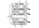
- the clock count type associative memory 10 includes a memory unit 11, a row decoder 12, a column decoder 13, a read / write circuit 14, and a search data storage circuit 15.
- the memory unit 11 includes a reference data storage circuit (Storage Cell: SC) SC 11 to SC 1W , SC 21 to SC 2W ,..., SC R1 to SC RW , a distance arithmetic circuit (absolute value difference arithmetic circuit) (Distance Processor: DP) DP 11 to DP 1W , DP 21 to DP 2W ,..., DP R1 to DP RW , and distance / clock number conversion circuits DC 1 to DC R are included.
- W and R are each an integer of 2 or more.
- the distance calculation circuits DP 11 to DP 1W are provided corresponding to the reference data storage circuits SC 11 to SC 1W , respectively.
- the distance calculation circuits DP 21 to DP 2W are provided corresponding to the reference data storage circuits SC 21 to SC 2W , respectively.
- the distance calculation circuits DP R1 to DP RW are provided corresponding to the reference data storage circuits SC R1 to SC RW , respectively.
- the distance / clock number conversion circuit DC 1 is provided corresponding to the distance calculation circuits DP 11 to DP 1W .
- the distance / clock number conversion circuit DC 2 is provided corresponding to the distance calculation circuits DP 21 to DP 2W .
- the distance / clock number conversion circuit DC R is provided corresponding to the distance calculation circuits DP R1 to DP RW .
- Reference data storage circuits SC 11 to SC 1W , SC 21 to SC 2W ,..., SC R1 to SC RW store reference data written by the row decoder 12, the column decoder 13, and the read / write circuit 14.
- the reference data storage circuits SC 11 to SC 1W store M ⁇ W (M is an integer of 1 or more) bits of reference data 1, and the reference data storage circuits SC 21 to SC 2W have M ⁇ W bits.
- the reference data 2 is stored, and the reference data storage circuits SC R1 to SC RW store the M ⁇ W bit reference data R in the same manner. That is, each of the reference data storage circuits SC 11 to SC 1W , SC 21 to SC 2W ,..., SC R1 to SC RW stores M ⁇ W bits of the reference data.
- the distance calculation circuits DP 11 to DP 1W include M ⁇ W bit reference data 1 stored in the reference data storage circuits SC 11 to SC 1W , M ⁇ W bit search data stored in the search data storage circuit 15, and Is calculated by a method described later.
- the distance calculation circuits DP 21 to DP 2W search for the M ⁇ W bit reference data 2 stored in the reference data storage circuits SC 21 to SC 2W and the M ⁇ W bit search stored in the search data storage circuit 15. The distance from the data is calculated by the method described later.
- the distance calculation circuits DP R1 to DP RW perform the M ⁇ W bit reference data R stored in the reference data storage circuits SC R1 to SC RW and the M ⁇ W stored in the search data storage circuit 15.
- the distance calculation circuits DP 11 to DP 1W output the distance between the reference data 1 and the search data to the distance / clock number conversion circuit DC 1 as an M ⁇ W bit distance signal.
- the distance calculation circuits DP 21 to DP 2W output the distance between the reference data 2 and the search data to the distance / clock number conversion circuit DC 2 as an M ⁇ W bit distance signal.
- the distance calculation circuits DP R1 to DP RW output the distance between the reference data R and the search data to the distance / clock number conversion circuit DC R as an M ⁇ W bit distance signal.
- Each of the distance calculation circuits DP 11 to DP 1W calculates the distance between the reference data 1 and the search data using the following equation.
- the distance calculation circuits DP 11 to DP 1W calculate the distance between the M ⁇ W bit reference data 1 and the M ⁇ W bit search data by M bits, and each has a bit length of M bits.
- the W distance signals D 1j are output to the distance / clock number conversion circuit DC 1 .
- the distance calculation circuits DP 21 to DP 2W ,... And the distance calculation circuits DP R1 to DP RW each calculate the distance between the reference data 2 to R and the search data using the equation (1).
- the distance calculation circuits DP 21 to DP 2W ,... And the distance calculation circuits DP R1 to DP RW also respectively convert the W distance signals D 2j to D Rj each having a bit length of M bits into a distance / clock number conversion circuit. DC 2 and outputs it to the ⁇ DC R.
- the distance / clock number conversion circuit DC 1 receives W distance signals D 1j from the distance calculation circuits DP 11 to DP 1W, and calculates the clock number CN_total1 of the clock signal CLK corresponding to the sum of square values of the distance signals D 1j. It counts by the method mentioned later. Then, it outputs a match signal M 1 showing a timing of counting the number of clocks CN_total1.
- the distance calculation circuit DP 21 ⁇ received a W number of distance signal D 2j from DP 2W, the clock number CN_total2 of the clock signal CLK corresponding to the sum of the square of the distance signal D 2j It counts by the method mentioned later. Then, it outputs a match signal M 2 showing a timing of counting the number of clocks CN_total2.
- the distance / clock number conversion circuit DC R receives W distance signals D Rj from the distance calculation circuits DP R1 to DP RW and receives a clock signal corresponding to the sum of square values of the distance signals D Rj.
- the clock number CN_totalR of CLK is counted by a method described later. Then, it outputs a match signal M R indicative of the timing of counting the number of clocks CN_totalR.
- the row decoder 12 specifies an address in the row direction of the memory unit 11.
- the column decoder 13 specifies an address in the column direction of the memory unit 11.
- the read / write circuit 14 writes the reference data to the reference data storage circuits SC 11 to SC 1W , SC 21 to SC 2W ,..., SC R1 to SC RW designated by the row decoder 12 and the column decoder 13 and performs a search. Data is written into the search data storage circuit 15.
- the search data storage circuit 15 stores the search data (M ⁇ W bit data) written by the read / write circuit 14.
- Figure 3 shows a schematic configuration of a distance / clock number converting circuit DC 1 according to an example. Note that the distance / well each clock number conversion circuits DC 2 ⁇ DC R, has the same configuration as the distance / clock number conversion circuit DC 1 shown in FIG.
- Distance / clock number converting circuit DC 1 includes a buffer 121 ⁇ 12W, a counter coincidence detection circuits 131 ⁇ 13W.
- the buffer 121 receives a search start signal SB from a control circuit (not shown) of the k-nearest neighbor associative memory 100 and receives a clock signal CLK from a clock generator circuit (not shown) built in the k-nearest neighbor associative memory 100. . Then, when the search start signal SB transits from the L level to the H level, the buffer 121 outputs the received clock signal CLK to the buffer 122 and the counter coincidence detection circuit 131. When the buffer 122 receives the clock signal CLK from the buffer 121 and receives an H level coincidence signal (DETECT1) described later from the counter coincidence detection circuit 131, the buffer 122 receives the clock signal CLK from the buffer 123 (not shown) and the counter coincidence detection circuit.
- DETECT1 H level coincidence signal
- the buffer 12W receives the clock signal CLK from the buffer 12W-1 (not shown), and receives an H level coincidence signal (DETECTW ⁇ ) described later from the counter coincidence detection circuit 13W-1 (not shown). 1), the clock signal CLK is output to the counter coincidence detection circuit 13W.
- Counter coincidence detection circuits 131 to 13W are provided corresponding to distance calculation circuits DP 11 to DP 1W , respectively.
- the counter match detection circuits 131 to 13W are connected in series.
- a schematic configuration of the counter coincidence detection circuits 131 to 13W will be described.
- the counter coincidence detection circuit 131 includes a clock number conversion circuit 131a, a counter 131b, and a coincidence detection circuit 131c.
- Counter coincidence detection circuit 132 includes a clock number conversion circuit 132a, a counter 132b, and a coincidence detection circuit 132c.
- the function of each component will be described.
- the clock number conversion circuit 131 a receives the distance signal D 11 having a bit length of M bits from the distance calculation circuit DP 11 and the clock signal CLK from the buffer 121. Clock number conversion circuit 131a counts the number of clocks of the clock signal CLK, and at the timing of detecting the number of clocks to match the distance indicated by the distance signal D 11, performs a process of outputting the H-level coincidence detection signal to the counter 131b . The clock number conversion circuit 131a repeats this process until an H level coincidence signal (DETECT1) is output from the coincidence detection circuit 131c, which will be described later, and stops operating when the H level coincidence signal (DETECT1) is output. To do.
- the counter 131b counts up the counter value every time the coincidence detection signal from the clock number conversion circuit 131a rises, and outputs the count value to the coincidence detection circuit 131c.
- Coincidence detection circuit 131c receives the counter value from the counter 131b, receives the distance signal D 11 having a bit length of M bits from the distance computing circuit DP 11.
- Coincidence detection circuit 131c compares the distance and counter value distance signal D 11 indicates, when the distance signal D 11 is the distance the counter value indicating the match, H-level coincidence signal (DETECT1) the number of clocks conversion The data is output to the circuit 131a and the buffer 122.
- the distance a counter value distance signal D 11 indicates and is when they do not match, outputs L-level coincidence signal (DETECT1) to the clock number conversion circuit 131a and the buffer 122.
- the clock number conversion circuit 132 a is driven when it receives the clock signal CLK from the buffer 122.
- Clock number conversion circuit 132a receives the distance signal D 12 having a bit length of M bits from the distance calculation circuit DP 12.
- a clock number conversion circuit 132a counts the number of clocks of the clock signal CLK, the clock number that matches the distance the distance signal D 12 indicates the timing of detecting the coincidence of the H-level counter 132b Processing to output a detection signal is performed.
- the clock number conversion circuit 132a repeats this process until an H level coincidence signal (DETECT2) is output from the coincidence detection circuit 132c described later.
- the clock number conversion circuit 132a stops operating when the H level coincidence signal (DETECT2) is output.
- the counter 132b counts up the counter value every time the coincidence detection signal from the clock number conversion circuit 132a rises, and outputs the count value to the coincidence detection circuit 132c.
- Coincidence detection circuit 132c receives the counter value from the counter 132b, receives the distance signal D 12 having a bit length of M bits from the distance calculation circuit DP 12.
- Coincidence detection circuit 132c compares the distance and counter value distance signal D 12 indicates, when the distance signal the distance and counter value D 12 indicates a match, the number of clocks converts H level coincidence signal (DETECT2) and outputs to the circuit 132a and the buffer 122, and outputs H level of the coincidence signal (DETECT2) as a match signal M 1.
- the coincidence detection circuit 132c includes a distance and counter value distance signal D 12 is indicated when there is no match, and outputs L-level coincidence signal (DETECT2) to the clock number conversion circuit 132a.
- the distance calculation circuit DP 11 distance signal D 11 of M bits indicating the distance "2" from is output
- the distance calculation circuit DP 12 distance signal D 12 of M bits indicating the distance "3" from is output
- the clock number conversion circuit 131 a receives the M-bit distance signal D 11 indicating the distance “2”, and counts the number of clocks matching the distance “2” in synchronization with the clock of the clock signal CLK from the buffer 121.
- the clock number conversion circuit 131a outputs an H level coincidence detection signal when the counted number of clocks coincides with the distance.
- the counter 131b counts up the count value and outputs a counter value indicating “1” to the coincidence detection circuit 131c.
- the coincidence detection circuit 131c from the L-level coincidence signal (DETECT1) is output.
- the clock number conversion circuit 131a When the output coincidence detection signal becomes L level, the clock number conversion circuit 131a resets the counted clock number. Then, the clock number conversion circuit 131a again counts the clock number of the clock signal CLK, and outputs an H level coincidence detection signal to the counter 131b when the counted clock number coincides with the distance “2”. When the coincidence detection signal rises, the counter 131b counts up the counter value and outputs a counter value indicating “2” to the coincidence detection circuit 131c.
- Coincidence detection circuit 131c since the distance signal D 11 indicates the distance "2" and the counter value and "2" coincide, outputs a coincidence signal (DETECT1) in the buffer 122 and the clock number conversion circuit 131a. That is, an H level coincidence signal (DETECT1) is output at the timing when the number of clocks from the start of search becomes “4”. Then, the clock number conversion circuit 131a stops its operation in response to the H level coincidence signal (DETECT1).
- the buffer 122 receives the H level coincidence signal (DETECT1) from the coincidence detection circuit 131c, and outputs the clock signal CLK to the clock number conversion circuit 132a.
- the clock number conversion circuit 132 a counts the number of clocks of the clock signal CLK in synchronization with the clock of the clock signal CLK from the buffer 122.
- Clock number converting circuit 132a the distance receives the distance signal D 12 of M bits indicating "3", at the timing when the number of clock count matches the distance "3”, and outputs the H-level coincidence detection signal to the counter 132b .
- the coincidence detection signal from the clock number conversion circuit 132a rises, the counter 132b counts up the counter value and outputs a counter value indicating “1” to the coincidence detection circuit 132c.
- the match detection circuit 132c outputs an L level match signal (DETECT2).
- the clock number conversion circuit 132a resets the counted clock number when the output coincidence detection signal becomes L level. Then, the clock number conversion circuit 132a again counts the clock number of the clock signal CLK, and outputs an H level coincidence detection signal to the counter 132b when the counted clock number coincides with the distance “3”. When the coincidence detection signal from the clock number conversion circuit 132a rises, the counter 132b counts up the counter value and outputs a counter value indicating “2” to the coincidence detection circuit 132c. At this time, since the distance “3” and the counter value “2” do not match, the match detection circuit 132c outputs an L level match signal (DETECT2).
- the clock number conversion circuit 132a When the coincidence detection signal becomes L level, the clock number conversion circuit 132a resets the counted clock number again and counts the clock signal CLK. When the counted clock number coincides with the distance “3”, the counter 132b becomes H level. The coincidence detection signal is output. Then, the clock number conversion circuit 132a stops its operation in response to the H level coincidence signal (DETECT2). When the coincidence detection signal from the clock number conversion circuit 132a rises, the counter 132b counts up the counter value and outputs a counter value indicating “3” to the coincidence detection circuit 132c.
- the distance / clock number conversion circuit DC 1 generally receives W distance signals D 11 to D 1W . Each of the W distance signals D 11 to D 1W has a bit length of M bits. Therefore, distance / clock number conversion circuit DC 1 receives distance signals D 11 D 12 ... D 1W having a bit length of M ⁇ W bits.
- counter match detection circuit 131 only the number of times the distance signal D 11 is equal to the distance indicated, repeatedly counting the number of clocks that matches the distance.
- the counter match detection circuits 132 to 13W receive the match signal from the counter match detection circuits 131 to 13W-1, respectively, and then match the number of clocks that match the distance signals D 12 to D 1W to the distance, respectively. Count repeatedly.
- the distance / clock number conversion circuit overall number of clocks CN_total1 counted in DC 1 is equal to the sum of the number of clocks is counted in each of the counter match detection circuits 131 ⁇ 13W.
- the number of clocks counted in each of the counter coincidence detection circuits 131 to 13W corresponds to the square value of each distance indicated by the distance signals D 11 to D 1W, and thus is counted in the distance / clock number conversion circuit DC 1 .
- the total clock number CN_totalR represents the sum of square values of the distance signals D 11 to D 1W .
- the counter coincidence detection circuit 132 outputs the match signal M 1 indicating the timing of the number of clocks counted by the counter coincidence detection circuits 131 and 132 as a whole according to the Euclidean distance n Er .
- FIG. 5 is a timing chart of a match signal according to an example.
- Distance / clock number conversion circuits DC 1 ⁇ DC R as shown in FIG. 5, synchronization and outputs, for example, match signal M 1 ⁇ M R respectively clock signal CLK.
- the clock count associative memory 10 having the above configuration is merely an example, and any clock count associative memory capable of outputting as shown in FIG. 5 may be used.
- the k neighborhood search circuit 20 includes a match signal count circuit 21, a k-match signal number match detection circuit 22, and a match signal holding circuit 23.
- the match signal count circuit 21 is a circuit that counts the number of active match signals among the R match signals output from the clock count associative memory 10.
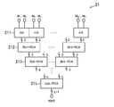
- FIG. 6 shows a schematic configuration of the match signal count circuit 21 according to an example.
- the match signal count circuit 21 can be configured as an adder tree circuit in which a plurality of adders are connected in a tree shape.
- R / 2 half adders (HA) 211 are arranged at the leaf nodes of the adder tree circuit.
- Each adder 211 receives 2 bits of R match signals. For example, a match signal M 1 corresponding to the reference data 1 and a match signal M 2 corresponding to the reference data 2 are input to the leftmost adder 211 in FIG. 6, and the reference data R ⁇ 1 is input to the rightmost adder 211.
- the corresponding match signal MR -1 and the match signal MR corresponding to the reference data R are input.
- R / 2 two 2-bit carry propagation adders (2-bit-RCA) 212 are arranged.
- Each adder 212 receives a 2-bit output from each of the two adders 211 in the previous stage (leaf node).
- Lbit-RCA 1 L-bit carry propagation adder 21L is arranged at the root node of the L stage of the adder tree circuit.
- the adder 21L receives L-bit outputs from the two adders at the previous stage (L-1 stage).
- NMS Number of Match Signals
- the match signal count circuit 21 is a circuit having the longest delay time among the components of the k-nearest neighbor associative memory 100. By configuring the match signal count circuit 21 as an adder tree circuit as described above, The delay time can be suppressed to the logarithmic order of the total number of match signals. Therefore, the delay time of the match signal count circuit 21 is such that it does not cause a problem in practice.
- the k-match signal number coincidence detection circuit 22 is a circuit that detects that the count value of the match signal count circuit 21 coincides with k. Note that the count value of the match signal count circuit 21 is represented by the above NMS, and k can be given from the outside.
- FIG. 7 shows a schematic configuration of the k-match signal number coincidence detection circuit 22 according to an example.
- k is given as a 4-bit value.
- the k-match signal number coincidence detection circuit 22 includes four 1-bit coincidence detection circuits 221 that compare corresponding bits of k and NMS.
- Each 1-bit coincidence detection circuit 221 is a circuit having 1-bit inputs A and B and 1-bit outputs X and Y.
- the corresponding bit of NMS is input to A, and the corresponding bit of k is input to B.
- the truth table of inputs A and B and outputs X and Y is as shown in Table 1.
- each 1-bit match detection circuit 221 outputs 1 to Y if the corresponding bit of NMS matches the corresponding bit of k, and outputs 1 to X if the corresponding bit of NMS is larger than the corresponding bit of k. .
- the 1-bit coincidence detection circuit 221 other than the most significant bit of k, the logical product of the corresponding bit of NMS and the output Y of the 1-bit coincidence detection circuit 221 of higher bits is input to A. . That is, the corresponding bit of the MSN is masked by the output Y of the 1-bit coincidence detection circuit 221 of the higher order bits. Therefore, as long as NMS and k do not match in the upper bits, the detection of matching between the lower bits of NMS and k is not performed. This is because, considering that NMS increases with time, it is not necessary to detect a match between NMS and the lower bits of k while NMS is smaller than k, and it is only necessary to detect a match in order from the upper bit. . In this way, by adopting a method of proceeding to the lower bit after seeing the match of the upper bit, unnecessary operation of the 1-bit match detection circuit 221 can be suppressed and power consumption can be reduced.
- each 1-bit match detection circuit 221 is input to the AND gate 222, and the logical product of all the outputs Y is calculated.
- the output of the AND gate 222 changes to H level.
- the output of the AND gate 222 is clocked (CLK) into the D flip-flop 224.
- the search start signal SB is input to the D flip-flop 224 (D).
- the D flip-flop 224 holds the search start signal SB at the H level according to the clock input. To do.
- the output (Q) of the D flip-flop 224 is output as a stop signal stop.
- the stop signal stop can be used as a timing signal for holding the match signal by the match signal holding circuit 23.
- the stop signal stop can be used as a control signal for stopping the operation of the clock count associative memory 10. After the number of active match signals reaches k, the clock count associative memory 10 may no longer operate. Therefore, the clock count type associative memory 10 is configured such that, for example, the supply of the clock signal CLK is cut off when the stop signal stop is received, thereby suppressing unnecessary operations of the clock count type associative memory 10 and consuming it. Electric power can be reduced.
- each 1-bit match detection circuit 221 is input to the OR gate 223a, and the logical sum of all the outputs X is calculated.
- the output of the OR gate 223a transitions to the H level.
- all the remaining upper bits of the NMS are input to the OR gate 223b, and the logical sum of these bits is calculated.
- the output of OR gate 223b transitions to H level.
- the OR gate 223c calculates the logical sum of the outputs of the OR gate 223a and the OR gate 223b.
- the output of the OR gate 223c is output as an abnormal signal abnormal. That is, when NMS exceeds k, an abnormal signal abnormal is output.
- the abnormal signal abnormal can be used for an instruction to redo k neighborhood search.
- the abnormal signal abnormal is clocked (CLK) into the D flip-flop 224. Thereby, the stop signal stop is output in accordance with the output of the abnormal signal abnormal.
- the abnormal signal abnormal is masked by the inverted logic of the output (Q) of the D flip-flop 224. That is, when NMS and K completely match before the abnormal signal abnormal is output and the stop signal stop is output, the abnormal signal abnormal is not output even if NMS exceeds k after that.
- a reset signal RST that is commonly used in the k-nearest neighbor associative memory 100 is input.
- the match signal holding circuit 23 receives R match signals output from the clock count associative memory 10, and the k-match signal number match detection circuit 22 determines the count value of the match signal count circuit 21. It holds R match signals when it is detected that they match k.
- FIG. 8 shows a configuration of the match signal holding circuit 23 according to an example.
- the match signal holding circuit 23 includes R D flip-flops 231 that hold R match signals M 1 to MR output from the clock count associative memory 10.
- a match signal is input as data (D)
- a stop signal stop is input as a clock (CLK).
- the outputs (Q) of the R D flip-flops 231 are input to the k-nearest clustering circuit 30 as R match signals M 1 to MR.
- each D flip-flop 231 is reset to an initial state upon receiving a reset signal RST.
- the k neighborhood clustering circuit 30 includes a class data memory 31, X class counters 32, a class identification circuit 33, and a maximum counter detection circuit 34.
- the class data memory 31 is a circuit that holds R class data (class data 1, class data 2,..., Class data R) representing each class of R reference data.
- Each class counter 32 is a circuit for counting the number of data of the corresponding class.
- the total number of classes is X (X is an integer of 2 or more).
- the class identification circuit 33 sequentially selects the active k match signals held by the k neighborhood search circuit 20 (more specifically, the match signal holding circuit 23), and class data corresponding to the selected match signal is class data. This circuit reads out from the memory 31 and counts up the class counter 32 corresponding to the class represented by the read class data.
- FIG. 9 shows a schematic configuration of the class data memory 31, the class counter 32, and the class identification circuit 33 according to an example.
- the memory unit 311 includes class data storage circuits S 11 to S 1Q , S 21 to S 2Q ,..., S R1 to S RQ composed of SRAM or the like.
- Q is an integer of 2 or more.
- the row selection circuit 312 specifies an address in the row direction of the memory unit 311.
- the column decoder 313 specifies an address in the column direction of the memory unit 311.
- Read / write circuit 314 reads / writes class data to / from class data storage circuits S 11 to S 1Q , S 21 to S 2Q ,..., S R1 to S RQ designated by row selection circuit 312 and column decoder 313. To do.
- the R match signal detection circuits 331 are provided corresponding to each of the R match signals held by the k neighborhood search circuit 20 (more specifically, the match signal holding circuit 23).
- Each match signal detection circuit 331 is a circuit that detects that a corresponding match signal is active and outputs a selection signal act for selecting class data corresponding to the match signal to the class data memory 31.
- the class data 1 is selected and output in the class data memory 31 by the selection signal act 1 output from the match signal detection circuit 331 to which the match signal M 1 is input.
- the class data 2 is selected and output in the class data memory 31 by the selection signal act 2 output from the match signal detection circuit 331 to which the match signal M 2 is input.
- the selection signal act R a match signal M R is output from the match signal detecting circuit 331 is inputted, the class data R is selected in the class data memory 31, is output.
- the register 3312 holds 0 as an initial value. Therefore, when the match signal M i is inactive, both coincidence signal match becomes H level match. At this time, the output of the AND gate 3313 becomes H level, and the operation start signal next i ⁇ 1 is supplied to the next - stage match signal detection circuit 331. Further, the output of the AND gate 3314 becomes L level. That is, the class data selection signal act i is not output. Thus transmission, when the match signal M i is inactive, the match signal detection circuit 331 without outputting the selection signal of the class data, the input operation start signal immediately in the next stage of the match signal detection circuit 331 To do.
- the match signal M i is when active, both the coincidence signal match because it does not match the L level.
- the output of the AND gate 3313 becomes L level, and the operation start signal next i ⁇ 1 at the H level is input, whereby the selection signal act i at the H level is output from the AND gate 3314.
- a clock signal CLK is connected to the register 3312 via a buffer 3315 and a buffer 3316 connected in series.
- the buffer 3315 supplies the clock signal CLK to the buffer 3316.
- the buffer 3316 supplies the clock signal CLK to the register 3312.
- the register 3312 changes the hold value to 1 when it receives the clock signal CLK.
- coincidence signal match becomes an L level and retention values of active match signals M i and the register 3312 match.
- the output of the AND gate 3313 becomes H level, and the operation start signal next i ⁇ 1 is supplied to the next - stage match signal detection circuit 331. Further, the output of the AND gate 3314 becomes L level.
- the class data selection signal act i transitions to the L level.
- the match signal detection circuit 331 after outputting the selection signal of the class data after one clock period, the next stage of the match signal to input the operation start signal detecting circuit 331 To communicate.
- the class data selection signal output at this time is at the H level for one clock cycle.
- the count values Cn 1 to Cn X of the X class counters 32 indicate the number of neighborhoods of each class. That is, by referring to the count values Cn 1 to Cn X , the number of votes (data number) of each class can be known.
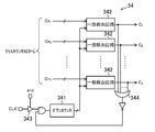
- the maximum counter detection circuit 34 is a circuit for finding a class counter having the maximum count value from among the X class counters 32.
- Each coincidence detection circuit 342 is a circuit that detects coincidence between the count value of the corresponding class counter 32 and the count value of the down counter 341 and outputs coincidence signals C 1 to C X. When each coincidence detection circuit 342 detects a coincidence, it makes the coincidence signals C 1 to C X transition to the H level.
- the output signals of the X coincidence detection circuits 342 are input to the OR gate 344, and their logical sum is calculated.
- the clock signal CLK input to the down counter 341 is masked by logical inversion of the output of the OR gate 344. That is, while the count value of the down counter 341 is being counted down, any one of the X match detection circuits 342 matches the count value of the down counter 341 with the count value of the corresponding class counter 32. When detected, the count operation of the down counter 341 is stopped. Thereby, only the class counter 32 holding the maximum count value can be detected.
- the coincidence signals C 1 to C X those that are at the H level represent the class of search data determined based on the k-nearest neighbor method.
- FIG. 12 shows a schematic configuration of a maximum counter detection circuit 34 according to another example.
- the maximum counter detection circuit 34 can also be configured as a tournament circuit in which a plurality of maximum value selection circuits 345 are connected in a tree shape.
- FIG. 13 shows a schematic configuration of a maximum value selection circuit 345 according to an example.
- Maximum value selection circuit 345 includes a comparison circuit 346 and a multiplexer 347.
- the multiplexer 347 outputs a signal A & i when A ⁇ B, and outputs a signal B & j when A ⁇ B. That is, as the signal C, a signal obtained by combining the count value max (A, B) of the class counter 32 having the larger counter value and the identification number index (i or j) of the class counter is output. Note that the multiplexer 347 may output the signal A & i when A> B, and may output the signal B & j when A ⁇ B.
- X / 2 maximum value selection circuits 345 are arranged at the leaf nodes of the tournament circuit. Each leaf node maximum value selection circuit 345 receives a signal obtained by combining the counter values of two adjacent class counters 32 of the X class counters 32 and the identification numbers of the two class counters 32.
- Each maximum value selection circuit 345 in the second stage receives a signal output from two maximum value selection circuits 345 adjacent to the leaf node.
- One maximum value selection circuit 345 is arranged at the root node of the tournament circuit. Then, a signal obtained by combining the maximum count value max (Cn 1 ,..., Cn X ) of the X class counters 32 and the class index that is the identification number of the class counter 32 is output from the maximum value selection circuit 345 of the root node. Is done.
- the maximum counter detection circuit 34 configured as described above is particularly suitable for high-speed processing because the maximum value of the X class counters 32 can be determined in one clock cycle.
- the k neighborhood search circuit 20 stores R match signals output from the clock count associative memory 10 as 1-bit information, and therefore distance information is lost. Therefore, for example, a counter may be provided in the k neighborhood search circuit 20 to hold time information (that is, time-converted distance information) until each match signal becomes active. In that case, class information can be weighted so as to increase the weight of reference data that is closer to the search data by using time information, and more advanced class discrimination can be performed. It is also possible to apply the k-nearest neighbor method to k or fewer reference data corresponding to the k match signals that have become active, excluding those having a distance from the search data that is greater than or equal to a threshold value.
Landscapes
- Radar Systems Or Details Thereof (AREA)
Abstract
k近傍法連想メモリ(100)は、R個の参照データを保持しており、R個の参照データのそれぞれについて、与えられた検索データとの距離に応じたクロック数の経過後にアクティブとなるマッチ信号を出力するクロックカウント式連想メモリ(10)と、クロックカウント式連想メモリから出力されるR個のマッチ信号のうちいずれかK個のマッチ信号がアクティブになったことを検出し、そのときのR個のマッチ信号を保持するk近傍検索回路(20)と、R個の参照データのそれぞれのクラスを表すR個のクラスデータからk近傍検索回路が保持するアクティブのk個のマッチ信号のそれぞれに対応するk個のクラスデータを選択し、k個のクラスデータをクラス別に分類した場合においてデータ数が最大となるクラスを判定するk近傍クラスタリング回路(30)とを備えている。
Description
本発明は、連想メモリに関し、特に、k近傍法を効果的に実現する連想メモリに関する。
近年、文字認識・画像認識などに代表されるパターンマッチングを必要とするアプリケーションが大変注目されている。特に、パターンマッチングをLSI(Large Scale Integrated circuit)上で実現することにより、将来、人工知能およびモバイル機器などの高機能アプリケーションに適用可能になり、この技術の実現は、非常に注目を浴びている。
パターンマッチングでは、データベースに保存された複数の参照データの中から、完全に検索データと一致するパターンを検索する「完全一致検索処理」と、検索データと最も類似するパターンを検索する「最類似検索処理」とがある。
前者は、CAM(Content Addressable Memory)と呼ばれ、ネットワークルータのIPアドレステーブルのルーティングおよびプロセッサのキャッシュなどの実現に用いられる。人間の脳のような柔軟な検索・比較をコンピュータに処理させるには、後者の最類似検索処理を実現することが必要不可欠である。このような柔軟な比較を実現する機能を持つメモリのことを特に連想メモリ(Associative Memory)と呼ぶ。
連想メモリの例として、検索データと参照データとのマンハッタン距離またはユークリッド距離を用いて最類似検索処理を行うものが知られている(非特許文献1参照)。また、連想メモリにk近傍探索を取り入れたものが知られている(非特許文献2参照)。
S.Sasaki et al., "Digital Associative Memory for Word-Parallel Manhattan-Distance-Based Vector Quantization," ESSCIRC'2012, 2012, pp.185-188
M.A.Abedin et al., "Realization of K-Nearest-Matches Search Capability in Fully-Parallel Associative Memories," IEICE Trans. on Fundamentals, vol. E90-A, No.6, 2007, pp.1240-1243
パターン認識の分野において機械学習アルゴリズムとしてk近傍法がよく用いられる。k近傍法は、パターン認識において高い信頼性を持つ。従来技術では、連想メモリにおいてk近傍探索を取り入れているものの、k近傍法が実効的に実現されておらず、特にk近傍法に基づいたパターンのクラス分けまでは実現できていない。
上記問題に鑑み、本発明は、k近傍法を効果的に実現することができるk近傍法連想メモリを提供することを目的とする。
本発明の一局面に従ったk近傍法連想メモリは、R個の参照データを保持しており、前記R個の参照データのそれぞれについて、与えられた検索データとの距離に応じたクロック数の経過後にアクティブとなるマッチ信号を出力するクロックカウント式連想メモリと、前記クロックカウント式連想メモリから出力されるR個のマッチ信号のうちいずれかk個のマッチ信号がアクティブになったことを検出し、そのときの前記R個のマッチ信号を保持するk近傍検索回路と、前記R個の参照データのそれぞれのクラスを表すR個のクラスデータから前記k近傍検索回路が保持するアクティブのk個のマッチ信号のそれぞれに対応するk個のクラスデータを選択し、前記k個のクラスデータをクラス別に分類した場合においてデータ数が最大となるクラスを判定するk近傍クラスタリング回路とを備えている。
これによると、クロックカウント式連想メモリによって検索データと各参照データとの距離がクロック数に変換されて、距離に応じたタイミングで各参照データに対応するマッチ信号がアクティブとなり、k近傍検索回路によってより先にアクティブになったk個のマッチ信号が検出および保持され、k近傍クラスタリング回路によって当該k個のマッチ信号に対応するk個のクラスデータをクラス別に分類した場合にデータ数が最大となるクラスが判定される。このようにして、k近傍法に基づいた検索データのクラス分けが実現される。
本発明によると、LSI上にk近傍法を効果的に実装することができる。
以下、図面を参照しながら本発明を実施するための形態について説明する。なお、本発明は、以下の実施形態に限定されるものではない。
図1は、本発明の一実施形態に係るk近傍法連想メモリ100の概略構成を示す。本実施形態に係るk近傍法連想メモリ100は、クロックカウント式連想メモリ10と、k近傍検索回路20と、k近傍クラスタリング回路30とを備えている。
クロックカウント式連想メモリ10は、R個の参照データ(参照データ1,参照データ2,…,参照データR)を保持しており、これらR個の参照データのそれぞれについて、与えられた検索データとの距離に応じたクロック数の経過後にアクティブとなるマッチ信号を出力する回路である。なお、「距離」とはマンハッタン距離、ユークリッド距離などを含む。また、「アクティブ」とは、正論理では信号がLレベルからHレベルへと遷移することをいい、負論理では信号がHレベルからLレベルへと遷移することをいう。便宜のため、以下では正論理を前提に説明する。
k近傍検索回路20は、クロックカウント式連想メモリ10から出力されるR個のマッチ信号のうちいずれかk個のマッチ信号がアクティブになったことを検出し、そのときのR個のマッチ信号を保持する回路である。
k近傍クラスタリング回路30は、R個の参照データのそれぞれのクラスを表すR個のクラスデータ(クラスデータ1,クラスデータ2,…,クラスデータR)からk近傍検索回路20が保持するアクティブのk個のマッチ信号のそれぞれに対応するk個のクラスデータを選択し、これらk個のクラスデータをクラス別に分類した場合においてデータ数が最大となるクラスを判定する回路である。
k近傍法連想メモリ100は、上記3つの回路を備えることで、k近傍法に基づいて、与えられた検索データがいずれのクラスに分類されるかを判定することができる。以下、各回路の構成例について説明する。
≪クロックカウント式連想メモリ10の構成例≫
図2は、一例に係るクロックカウント式連想メモリ10の概略構成を示す。クロックカウント式連想メモリ10は、メモリ部11、行デコーダ12、列デコーダ13、読出/書込回路14、および検索データ保存回路15を含む。
図2は、一例に係るクロックカウント式連想メモリ10の概略構成を示す。クロックカウント式連想メモリ10は、メモリ部11、行デコーダ12、列デコーダ13、読出/書込回路14、および検索データ保存回路15を含む。
メモリ部11は、参照データ保存回路(Storage Cell:SC)SC11~SC1W,SC21~SC2W,…,SCR1~SCRWと、距離演算回路(絶対値差演算回路)(Distance Processor:DP)DP11~DP1W,DP21~DP2W,…,DPR1~DPRWと、距離/クロック数変換回路DC1~DCRとを含む。なお、WおよびRは、それぞれ、2以上の整数である。
距離演算回路DP11~DP1Wは、それぞれ、参照データ保存回路SC11~SC1Wに対応して設けられる。また、距離演算回路DP21~DP2Wは、それぞれ、参照データ保存回路SC21~SC2Wに対応して設けられる。以下、同様にして、距離演算回路DPR1~DPRWは、それぞれ、参照データ保存回路SCR1~SCRWに対応して設けられる。
距離/クロック数変換回路DC1は、距離演算回路DP11~DP1Wに対応して設けられる。距離/クロック数変換回路DC2は、距離演算回路DP21~DP2Wに対応して設けられる。以下、同様にして、距離/クロック数変換回路DCRは、距離演算回路DPR1~DPRWに対応して設けられる。
参照データ保存回路SC11~SC1W,SC21~SC2W,…,SCR1~SCRWは、行デコーダ12、列デコーダ13、および読出/書込回路14によって書き込まれた参照データを保存する。この場合、参照データ保存回路SC11~SC1Wは、M×W(Mは1以上の整数)ビットの参照データ1を保存し、参照データ保存回路SC21~SC2Wは、M×Wビットの参照データ2を保存し、以下、同様にして、参照データ保存回路SCR1~SCRWは、M×Wビットの参照データRを保存する。つまり、参照データ保存回路SC11~SC1W,SC21~SC2W,…,SCR1~SCRWのそれぞれは、参照データのM×Wビットを保存する。
距離演算回路DP11~DP1Wは、参照データ保存回路SC11~SC1Wに保存されたM×Wビットの参照データ1と、検索データ保存回路15に保存されたM×Wビットの検索データとの距離を後述する方法によって演算する。また、距離演算回路DP21~DP2Wは、参照データ保存回路SC21~SC2Wに保存されたM×Wビットの参照データ2と、検索データ保存回路15に保存されたM×Wビットの検索データとの距離を後述する方法によって演算する。以下、同様にして、距離演算回路DPR1~DPRWは、参照データ保存回路SCR1~SCRWに保存されたM×Wビットの参照データRと、検索データ保存回路15に保存されたM×Wビットの検索データとの距離を後述する方法によって演算する。そして、距離演算回路DP11~DP1W、距離演算回路DP21~DP2W、…、距離演算回路DPR1~DPRWにおける参照データと検索データとの距離の演算は、並列に行われる。
そして、距離演算回路DP11~DP1Wは、参照データ1と検索データとの距離をM×Wビットの距離信号として距離/クロック数変換回路DC1へ出力する。距離演算回路DP21~DP2Wは、参照データ2と検索データとの距離をM×Wビットの距離信号として距離/クロック数変換回路DC2へ出力する。以下、同様にして、距離演算回路DPR1~DPRWは、参照データRと検索データとの距離をM×Wビットの距離信号として距離/クロック数変換回路DCRへ出力する。
距離演算回路DP11~DP1Wのそれぞれは、参照データ1と検索データとの距離を次式を用いて演算する。

式(1)において、Drj(r=1~R,j=1~W)は、参照データと検索データとの距離(絶対値差)を表す。nMrは、参照データと検索データとのマンハッタン距離を示している。また、式(1)において、Injは、検索データであり、Rerjは、参照データである。各データInj、Rerjは、それぞれ、Mビットからなる。
このように、距離演算回路DP11~DP1Wは、M×Wビットの参照データ1と、M×Wビットの検索データとの距離をMビットずつ演算し、それぞれがMビットのビット長を有するW個の距離信号D1jを距離/クロック数変換回路DC1へ出力する。
距離演算回路DP21~DP2W、…および距離演算回路DPR1~DPRWも、同様にして、それぞれ、式(1)を用いて参照データ2~Rと検索データとの距離を演算する。そして、距離演算回路DP21~DP2W、…および距離演算回路DPR1~DPRWも、それぞれがMビットのビット長を有するW個の距離信号D2j~DRjをそれぞれ距離/クロック数変換回路DC2~DCRへ出力する。
距離/クロック数変換回路DC1は、距離演算回路DP11~DP1WからW個の距離信号D1jを受け、各距離信号D1jの二乗値の和に相当するクロック信号CLKのクロック数CN_total1を後述する方法によってカウントする。そして、そのクロック数CN_total1をカウントしたタイミングを示すマッチ信号M1を出力する。
距離/クロック数変換回路DC2は、距離演算回路DP21~DP2WからW個の距離信号D2jを受け、各距離信号D2jの二乗値の和に相当するクロック信号CLKのクロック数CN_total2を後述する方法によってカウントする。そして、そのクロック数CN_total2をカウントしたタイミングを示すマッチ信号M2を出力する。
以下、同様にして、距離/クロック数変換回路DCRは、距離演算回路DPR1~DPRWからW個の距離信号DRjを受け、各距離信号DRjの二乗値の和に相当するクロック信号CLKのクロック数CN_totalRを後述する方法によってカウントする。そして、そのクロック数CN_totalRをカウントしたタイミングを示すマッチ信号MRを出力する。
行デコーダ12は、メモリ部11の行方向のアドレスを指定する。列デコーダ13は、メモリ部11の列方向のアドレスを指定する。読出/書込回路14は、参照データを行デコーダ12および列デコーダ13によって指定された参照データ保存回路SC11~SC1W,SC21~SC2W,…,SCR1~SCRWに書き込むとともに、検索データを検索データ保存回路15に書き込む。
検索データ保存回路15は、読出/書込回路14によって書き込まれた検索データ(M×Wビットのデータ)を保存する。
図3は、一例に係る距離/クロック数変換回路DC1の概略構成を示す。なお、距離/クロック数変換回路DC2~DCRのそれぞれも、図3に示す距離/クロック数変換回路DC1と同様の構成を有する。距離/クロック数変換回路DC1は、バッファ121~12Wと、カウンタ一致検出回路131~13Wとを含む。
バッファ121は、k近傍法連想メモリ100の制御回路(図示せず)から検索開始信号SBを受け、k近傍法連想メモリ100に内蔵されたクロック発生回路(図示せず)からクロック信号CLKを受ける。そして、バッファ121は、検索開始信号SBがLレベルからHレベルに遷移すると、その受けたクロック信号CLKをバッファ122およびカウンタ一致検出回路131へ出力する。バッファ122は、クロック信号CLKをバッファ121から受け、カウンタ一致検出回路131から、後述するHレベルの一致信号(DETECT1)を受けると、クロック信号CLKをバッファ123(図示せず)およびカウンタ一致検出回路132へ出力する。以下、同様にして、バッファ12Wは、クロック信号CLKをバッファ12W-1(図示せず)から受け、カウンタ一致検出回路13W-1(図示せず)から、後述するHレベルの一致信号(DETECTW-1)を受けると、クロック信号CLKをカウンタ一致検出回路13Wへ出力する。
カウンタ一致検出回路131~13Wは、それぞれ、距離演算回路DP11~DP1Wに対応して設けられる。そして、カウンタ一致検出回路131~13Wは、直列に接続される。ここで、カウンタ一致検出回路131~13Wの概略構成について説明する。
図4は、一例に係るカウンタ一致検出回路131~13Wの概略構成を示す。本例は、W=2の場合を示している。カウンタ一致検出回路131は、クロック数変換回路131aと、カウンタ131bと、一致検出回路131cとを含む。カウンタ一致検出回路132は、クロック数変換回路132aと、カウンタ132bと、一致検出回路132cとを含む。以下、各構成の機能について説明する。
クロック数変換回路131aは、距離演算回路DP11からMビットのビット長を有する距離信号D11と、バッファ121からのクロック信号CLKとを受ける。クロック数変換回路131aは、クロック信号CLKのクロック数をカウントし、距離信号D11が示す距離と一致するクロック数を検出したタイミングで、カウンタ131bにHレベルの一致検出信号を出力する処理を行う。クロック数変換回路131aは、後述の一致検出回路131cからHレベルの一致信号(DETECT1)が出力されるまで、この処理を繰り返し行い、Hレベルの一致信号(DETECT1)が出力されると動作を停止する。
カウンタ131bは、クロック数変換回路131aからの一致検出信号が立ち上がるごとにカウンタ値をカウントアップさせ、そのカウント値を一致検出回路131cへ出力する。
一致検出回路131cは、カウンタ131bからカウンタ値を受け、距離演算回路DP11からMビットのビット長を有する距離信号D11を受ける。一致検出回路131cは、距離信号D11が示す距離とカウンタ値とを比較し、距離信号D11が示す距離とカウンタ値とが一致するときに、Hレベルの一致信号(DETECT1)をクロック数変換回路131aとバッファ122へ出力する。一致検出回路131cは、距離信号D11が示す距離とカウンタ値とが一致しないときは、Lレベルの一致信号(DETECT1)をクロック数変換回路131aとバッファ122へ出力する。
クロック数変換回路132aは、バッファ122からクロック信号CLKを受けると駆動する。クロック数変換回路132aは、距離演算回路DP12からMビットのビット長を有する距離信号D12を受ける。クロック数変換回路131aと同様、クロック数変換回路132aは、クロック信号CLKのクロック数をカウントし、距離信号D12が示す距離と一致するクロック数を検出したタイミングで、カウンタ132bにHレベルの一致検出信号を出力する処理を行う。クロック数変換回路132aは、後述の一致検出回路132cからHレベルの一致信号(DETECT2)が出力されるまで、この処理を繰り返し行う。クロック数変換回路132aは、Hレベルの一致信号(DETECT2)が出力されると動作を停止する。
カウンタ132bは、クロック数変換回路132aからの一致検出信号が立ち上がるごとにカウンタ値をカウントアップさせ、そのカウント値を一致検出回路132cへ出力する。
一致検出回路132cは、カウンタ132bからカウンタ値を受け、距離演算回路DP12からMビットのビット長を有する距離信号D12を受ける。一致検出回路132cは、距離信号D12が示す距離とカウンタ値とを比較し、距離信号D12が示す距離とカウンタ値とが一致するときに、Hレベルの一致信号(DETECT2)をクロック数変換回路132aとバッファ122へ出力するとともに、Hレベルの一致信号(DETECT2)をマッチ信号M1として出力する。また、一致検出回路132cは、距離信号D12が示す距離とカウンタ値とが一致しないときは、Lレベルの一致信号(DETECT2)をクロック数変換回路132aに出力する。
ここで、例えば、距離演算回路DP11から距離「2」を示すMビットの距離信号D11が出力され、距離演算回路DP12から距離「3」を示すMビットの距離信号D12が出力された場合の動作例について説明する。
クロック数変換回路131aは、距離「2」を示すMビットの距離信号D11を受け、バッファ121からのクロック信号CLKのクロックに同期して、距離「2」に一致するクロック数をカウントする。クロック数変換回路131aは、カウントしたクロック数と距離とが一致すると、Hレベルの一致検出信号を出力する。カウンタ131bは、一致検出信号が立ち上がると、カウント値をカウントアップし、「1」を示すカウンタ値を一致検出回路131cに出力する。このとき、距離信号D11が示す距離「2」とカウント値「1」とが一致しないため、一致検出回路131cからLレベルの一致信号(DETECT1)が出力される。
クロック数変換回路131aは、出力した一致検出信号がLレベルになると、カウントしたクロック数をリセットする。そして、クロック数変換回路131aは、再びクロック信号CLKのクロック数をカウントし、カウントしたクロック数が距離「2」と一致すると、カウンタ131bにHレベルの一致検出信号を出力する。カウンタ131bは、一致検出信号が立ち上がると、カウンタ値をカウントアップさせ、一致検出回路131cに「2」を示すカウンタ値を出力する。一致検出回路131cは、距離信号D11が示す距離「2」とカウンタ値「2」とが一致するため、一致信号(DETECT1)をバッファ122とクロック数変換回路131aに出力する。つまり、検索開始からのクロック数が「4」となるタイミングで、Hレベルの一致信号(DETECT1)が出力される。そして、クロック数変換回路131aは、Hレベルの一致信号(DETECT1)に応じて動作を停止する。
バッファ122は、一致検出回路131cからHレベルの一致信号(DETECT1)を受けて、クロック数変換回路132aにクロック信号CLKを出力する。クロック数変換回路132aは、バッファ122からのクロック信号CLKのクロックに同期して、クロック信号CLKのクロック数をカウントする。クロック数変換回路132aは、距離「3」を示すMビットの距離信号D12を受け、カウントしたクロック数が距離「3」と一致するタイミングで、Hレベルの一致検出信号をカウンタ132bに出力する。カウンタ132bは、クロック数変換回路132aからの一致検出信号が立ち上がると、カウンタ値をカウントアップさせ、一致検出回路132cに「1」を示すカウンタ値を出力する。このとき、距離「3」とカウンタ値「1」とが一致しないため、一致検出回路132cからLレベルの一致信号(DETECT2)が出力される。
クロック数変換回路132aは、出力した一致検出信号がLレベルになると、カウントしたクロック数をリセットする。そして、クロック数変換回路132aは、再びクロック信号CLKのクロック数をカウントし、カウントしたクロック数が距離「3」と一致すると、カウンタ132bにHレベルの一致検出信号を出力する。カウンタ132bは、クロック数変換回路132aからの一致検出信号が立ち上がると、カウンタ値をカウントアップさせ、一致検出回路132cに「2」を示すカウンタ値を出力する。このとき、距離「3」とカウンタ値「2」とが一致しないため、一致検出回路132cからLレベルの一致信号(DETECT2)が出力される。
クロック数変換回路132aは、一致検出信号がLレベルになると、再びカウントしたクロック数をリセットしてクロック信号CLKをカウントし、カウントしたクロック数が距離「3」と一致すると、カウンタ132bにHレベルの一致検出信号を出力する。そして、クロック数変換回路132aは、Hレベルの一致信号(DETECT2)に応じて動作を停止する。カウンタ132bは、クロック数変換回路132aからの一致検出信号が立ち上がると、カウンタ値をカウントアップさせ、一致検出回路132cに「3」を示すカウンタ値を出力する。一致検出回路132cは、距離「3」とカウント値「3」とが一致するために、Hレベルの一致信号(DETECT2)をクロック数変換回路132aに出力するとともに、マッチ信号M1を出力する。つまり、クロック数変換回路132aにおいてカウントされたクロック数は「9(=3+3+3)」であり、検索開始からクロック数「13(=4+9)」のタイミングでマッチ信号M1が出力される。
カウンタ一致検出回路131,132全体でカウントされるクロック数CN_total1「13」は、カウンタ一致検出回路131においてカウントするクロック数「4(=2+2)」と、カウンタ一致検出回路132においてカウントするクロック数「9(=3+3+3)」とを加算したものである。つまり、カウンタ一致検出回路131,132によって、距離「2」の二乗値と距離「3」の二乗値との和に一致するクロック数をカウントすることに相当する。
距離/クロック数変換回路DC1は、一般的に、W個の距離信号D11~D1Wを受ける。そして、W個の距離信号D11~D1Wのそれぞれは、Mビットのビット長を有する。したがって、距離/クロック数変換回路DC1は、M×Wビットのビット長を有する距離信号D11D12…D1Wを受ける。カウンタ一致検出回路131において、距離信号D11が示す距離に一致する回数分だけ、その距離に一致するクロック数を繰り返しカウントする。また、カウンタ一致検出回路132~13Wは、それぞれ、カウンタ一致検出回路131~13W-1から一致信号を受けた後に、距離信号D12~D1Wにそれぞれ一致するクロック数を、その距離に一致する回数だけ繰り返しカウントする。その結果、距離/クロック数変換回路DC1においてカウントされる全体のクロック数CN_total1は、カウンタ一致検出回路131~13Wのそれぞれにおいてカウントされたクロック数の和に等しい。カウンタ一致検出回路131~13Wのそれぞれにおいてカウントされたクロック数は、それぞれ、距離信号D11~D1Wが示す各距離の二乗値に相当するため、距離/クロック数変換回路DC1においてカウントされる全体のクロック数CN_totalRは、各距離信号D11~D1Wの二乗値の和を表している。
ここで、ユークリッド距離nErは、次式によって表される。

式(2)の右辺の|Inj-Rerj|2は、式(1)の右辺の|Inj-Rerj|において、検索データと参照データとの距離の二乗値に一致する。したがって、ユークリッド距離nErの演算は、上述したように、式(1)によって演算したW個の各距離について、距離に一致するクロック数をカウントする処理を距離に一致する回数だけ繰り返し行うことで実現される。そうすると、図4の例において、カウンタ一致検出回路132が、カウンタ一致検出回路131,132全体でカウントしたクロック数のタイミングを示すマッチ信号M1を出力することは、ユークリッド距離nErによって検索データに類似する参照データを検索し、検索データに類似する参照データを検出したことを示す信号を出力することに相当する。なお、距離/クロック数変換回路DC2~DCRのそれぞれも、距離/クロック数変換回路DC1の動作と同じ動作によって、それぞれ、マッチ信号M2~MRを出力する。
図5は、一例に係るマッチ信号のタイミングチャートである。距離/クロック数変換回路DC1~DCRは、図5に示すように、例えばマッチ信号M1~MRをそれぞれクロック信号CLKに同期して出力する。
なお、上記構成のクロックカウント式連想メモリ10は一例に過ぎず、図5に示したような出力が可能なクロックカウント式連想メモリであればよい。
≪k近傍検索回路20の構成例≫
図1に戻り、k近傍検索回路20は、マッチ信号カウント回路21と、k-マッチ信号数一致検出回路22と、マッチ信号保持回路23とを含む。
図1に戻り、k近傍検索回路20は、マッチ信号カウント回路21と、k-マッチ信号数一致検出回路22と、マッチ信号保持回路23とを含む。
マッチ信号カウント回路21は、クロックカウント式連想メモリ10から出力されるR個のマッチ信号のうちアクティブになったマッチ信号の数をカウントする回路である。
図6は、一例に係るマッチ信号カウント回路21の概略構成を示す。マッチ信号カウント回路21は、複数の加算器をツリー状に接続した加算器ツリー回路として構成することができる。加算器ツリー回路のリーフノードにはR/2個の半加算器(HA)211が配置される。各加算器211にはR個のマッチ信号のうちの2ビットが入力される。例えば、図6の左端の加算器211には参照データ1に対応するマッチ信号M1と参照データ2に対応するマッチ信号M2が入力され、右端の加算器211には参照データR-1に対応するマッチ信号MR-1と参照データRに対応するマッチ信号MRが入力される。
加算器ツリー回路の2段目にはR/22個の2ビットの桁上げ伝播加算器(2bit-RCA)212が配置される。各加算器212には前段(リーフノード)の2個の加算器211からそれぞれ2ビット出力が入力される。
加算器ツリー回路の3段目にはR/23個の3ビットの桁上げ伝播加算器(3bit-RCA)213が配置される。各加算器213には前段(第2段目)の2個の加算器212からそれぞれ3ビット出力が入力される。
加算器ツリー回路のL段目のルートノードには1個のLビットの桁上げ伝播加算器(Lbit-RCA)21Lが配置される。加算器21Lには前段(L-1段目)の2個の加算器からそれぞれLビット出力が入力される。
加算器21LからはL+1ビットのNMS(Number of Match Signals)が出力される。NMSが表す値は、R個のマッチ信号M1~MRのうちアクティブになったマッチ信号の数に相当する。
上記構成のマッチ信号カウント回路21によると、複数のマッチ信号が同時にアクティブになっても、それらマッチ信号の数を正確にカウントすることができる。
また、マッチ信号カウント回路21はk近傍法連想メモリ100の構成要素の中で最長の遅延時間を有する回路であるが、上記のようにマッチ信号カウント回路21を加算器ツリー回路として構成することにより、遅延時間をマッチ信号の総数の対数オーダーに抑えることができる。したがって、マッチ信号カウント回路21の遅延時間は実用上問題とならない程度のものである。
図1に戻り、k-マッチ信号数一致検出回路22は、マッチ信号カウント回路21のカウント値がkに一致したことを検出する回路である。なお、マッチ信号カウント回路21のカウント値は上記のNMSによって表され、また、kは外部から与えることができる。
図7は、一例に係るk-マッチ信号数一致検出回路22の概略構成を示す。本例において、kは4ビット値として与えられるものとする。k-マッチ信号数一致検出回路22は、kとNMSの対応するビットどうしを比較する4個の1ビット一致検出回路221を含む。
各1ビット一致検出回路221は、1ビット入力A,B、および1ビット出力X,Yを有する回路である。AにNMSの対応ビットが、Bにkの対応ビットが、それぞれ入力される。入力A,B、出力X,Yの真理値表は表1に示す通りである。

すなわち、各1ビット一致検出回路221は、NMSの対応ビットとkの対応ビットが一致すればYに1を出力し、NMSの対応ビットがkの対応ビットよりも大きければXに1を出力する。
kの最上位ビット以外の1ビット一致検出回路221において、NMSの対応ビットとそれよりも上位ビットの1ビット一致検出回路221の出力Yとの論理積がAに入力されるようになっている。すなわち、MSNの対応ビットがそれよりも上位ビットの1ビット一致検出回路221の出力Yによってマスクされるようになっている。このため、上位ビットにおいてNMSとkとが一致しない限り、NMSとkの下位ビットどうしの一致検出は行われない。これは、NMSが時間とともに増加することに鑑み、NMSがkよりも小さい間はNMSとkの下位ビットどうしの一致を検出する必要はなく、上位ビットから順に一致を検出すればよいためである。このように、上位ビットの一致を見て下位ビットに進むという方式を採用することにより、1ビット一致検出回路221の不要な動作を抑制して消費電力を低減することができる。
各1ビット一致検出回路221の出力YはANDゲート222に入力され、全出力Yの論理積が演算される。kとNMSとが完全一致したとき、ANDゲート222の出力がHレベルに遷移する。ANDゲート222の出力はDフリップフロップ224にクロック入力(CLK)される。Dフリップフロップ224には検索開始信号SBがデータ入力(D)されており、検索開始信号SBがHレベルの場合において、Dフリップフロップ224はクロック入力に応じてHレベルの検索開始信号SBを保持する。Dフリップフロップ224の出力(Q)は停止信号stopとして出力される。
後述するように、停止信号stopはマッチ信号保持回路23によるマッチ信号の保持のタイミング信号として利用することができる。また、停止信号stopはクロックカウント式連想メモリ10の動作を停止させる制御信号として利用することができる。アクティブのマッチ信号の数がk個に達した後はクロックカウント式連想メモリ10はもはや動作しなくてもよい。したがって、クロックカウント式連想メモリ10において、例えば、停止信号stopを受けたときにクロック信号CLKの供給を遮断するように構成することで、クロックカウント式連想メモリ10の不要な動作を抑制して消費電力を低減することができる。
各1ビット一致検出回路221の出力XはORゲート223aに入力され、全出力Xの論理和が演算される。1ビット一致検出回路221の少なくとも一つにおいてNMSの対応ビットがkの対応ビットよりも大きくなれば、ORゲート223aの出力がHレベルに遷移する。また、NMSの残りの全上位ビットはORゲート223bに入力され、これらビットの論理和が演算される。NMSの残りの全上位ビットにおいて少なくとも1ビットがHレベルとなった場合、ORゲート223bの出力がHレベルに遷移する。ORゲート223cは、ORゲート223aおよびORゲート223bの各出力の論理和を演算する。ORゲート223cの出力は、異常信号abnormalとして出力される。すなわち、NMSがkを超えたとき、異常信号abnormalが出力される。異常信号abnormalは、k近傍検索のやり直し指示などに利用することができる。また、異常信号abnormalはDフリップフロップ224にクロック入力(CLK)される。これにより、異常信号abnormalの出力に合わせて停止信号stopが出力される。
異常信号abnormalは、Dフリップフロップ224の出力(Q)の反転論理によってマスクされる。すなわち、異常信号abnormalが出力される前にNMSとKが完全一致して停止信号stopが出力された場合、その後NMSがkを超えても異常信号abnormalが出力されないようになっている。
Dフリップフロップ224のリセットを行うために、k近傍法連想メモリ100の共通に使用されるリセット信号RSTが入力される。
図1に戻り、マッチ信号保持回路23は、クロックカウント式連想メモリ10から出力されるR個のマッチ信号を受け、k-マッチ信号数一致検出回路22によってマッチ信号カウント回路21のカウント値がkに一致したことが検出されたときのR個のマッチ信号を保持する。
図8は、一例に係るマッチ信号保持回路23の構成を示す。マッチ信号保持回路23は、クロックカウント式連想メモリ10から出力されるR個のマッチ信号M1~MRのそれぞれを保持するR個のDフリップフロップ231を含む。各Dフリップフロップ231において、マッチ信号がデータ入力(D)されるとともに、停止信号stopがクロック入力(CLK)される。R個のDフリップフロップ231のそれぞれの出力(Q)は、R個のマッチ信号M1~MRとしてk近傍クラスタリング回路30に入力される。なお、図示していないが、各Dフリップフロップ231はリセット信号RSTを受けることで初期状態にリセットされる。
≪k近傍クラスタリング回路30の構成例≫
図1に戻り、k近傍クラスタリング回路30は、クラスデータメモリ31と、X個のクラスカウンタ32と、クラス識別回路33と、最大カウンタ検出回路34とを含む。
図1に戻り、k近傍クラスタリング回路30は、クラスデータメモリ31と、X個のクラスカウンタ32と、クラス識別回路33と、最大カウンタ検出回路34とを含む。
クラスデータメモリ31は、R個の参照データのそれぞれのクラスを表すR個のクラスデータ(クラスデータ1,クラスデータ2,…,クラスデータR)を保持する回路である。
各クラスカウンタ32は、対応するクラスのデータ数をカウントするための回路である。クラス数は、全部でX個(Xは2以上の整数)である。
クラス識別回路33は、k近傍検索回路20(より詳細にはマッチ信号保持回路23)が保持するアクティブのk個のマッチ信号を順次選択し、当該選択したマッチ信号に対応するクラスデータをクラスデータメモリ31から読み出し、当該読み出したクラスデータによって表されるクラスに対応するクラスカウンタ32をカウントアップする回路である。
図9は、一例に係るクラスデータメモリ31、クラスカウンタ32、およびクラス識別回路33の概略構成を示す。
クラスデータメモリ31は、メモリ部311、行選択回路312、列デコーダ313、および読出/書込回路314を含む。
メモリ部311は、SRAMなどで構成されるクラスデータ保存回路S11~S1Q,S21~S2Q,…,SR1~SRQを含む。なお、Qは、2以上の整数である。
クラスデータ保存回路S11~S1Q,S21~S2Q,…,SR1~SRQは、行選択回路312、列デコーダ313、および読出/書込回路314によって書き込まれたクラスデータを保存する。この場合、クラスデータ保存回路S11~S1Qは、N×Q(Nは1以上の整数)ビットのクラスデータ1を保存し、クラスデータ保存回路S21~S2Qは、N×Qビットのクラスデータ2を保存し、以下、同様にして、クラスデータ保存回路SR1~SRQは、N×QビットのクラスデータRを保存する。つまり、クラスデータ保存回路S11~S1Q,S21~S2Q,…,SR1~SRQのそれぞれは、クラスデータのNビットを保存する。
行選択回路312は、メモリ部311の行方向のアドレスを指定する。列デコーダ313は、メモリ部311の列方向のアドレスを指定する。読出/書込回路314は、行選択回路312および列デコーダ313によって指定されたクラスデータ保存回路S11~S1Q,S21~S2Q,…,SR1~SRQに対してクラスデータを読み書きする。
クラス識別回路33は、R個のマッチ信号検出回路331と、デマルチプレクサ332と、バッファ333とを含む。動作開始信号startがHレベルに遷移することで、バッファ333がクラス識別回路33にクロック信号CLKを供給する。これにより、クラス識別回路33は動作を開始する。また、クラス識別回路33によるクラス識別動作が終了すると終了信号endがHレベルに遷移する。
R個のマッチ信号検出回路331は、k近傍検索回路20(より詳細にはマッチ信号保持回路23)が保持するR個のマッチ信号のそれぞれに対応して設けられている。各マッチ信号検出回路331は、対応するマッチ信号がアクティブであることを検出してクラスデータメモリ31に当該マッチ信号に対応するクラスデータを選択する選択信号actを出力する回路である。
R個のマッチ信号検出回路331は、動作開始信号を伝搬するように直列に接続されている。すなわち、マッチ信号検出回路331は動作開始信号を次々に受けて順次動作するようになっている。初段のマッチ信号検出回路331は、動作開始信号startを動作開始信号next0として受けて動作を開始し、動作が終了すると次段(2段目)のマッチ信号検出回路331へ動作開始信号next1を出力する。2段目のマッチ信号検出回路331は、動作開始信号next1を受けて動作を開始し、動作が終了すると次段(3段目)のマッチ信号検出回路331へ動作開始信号next2を出力する。以下、同様にして、最終段(R段目)のマッチ信号検出回路331は、動作開始信号nextR-1を受けて動作を開始し、動作が終了すると動作開始信号nextRを出力する。動作開始信号nextRは終了信号endに相当する。
マッチ信号M1が入力されるマッチ信号検出回路331から出力される選択信号act1によって、クラスデータメモリ31においてクラスデータ1が選択され、出力される。マッチ信号M2が入力されるマッチ信号検出回路331から出力される選択信号act2によって、クラスデータメモリ31においてクラスデータ2が選択され、出力される。以下、同様にして、マッチ信号MRが入力されるマッチ信号検出回路331から出力される選択信号actRによって、クラスデータメモリ31においてクラスデータRが選択され、出力される。
図10は、一例に係るマッチ信号検出回路331の概略構成を示す。マッチ信号検出回路331は、一致検出回路3311と、レジスタ3312とを含む。一致検出回路3311は、レジスタ3312が保持する1ビット値とマッチ信号Miとの一致を検出して一致信号matchを出力する回路である。両者が一致する場合、一致信号matchはHレベルとなり、両者が一致しない場合、一致信号matchはLレベルとなる。一致信号matchおよびマッチ信号検出回路331に入力される動作開始信号nexti-1はANDゲート3313に入力されて論理積が演算される。ANDゲート3313の出力が、次段のマッチ信号検出回路331に供給される動作開始信号nextiとなる。また、一致信号matchの論理反転および動作開始信号nexti-1はANDゲート3314に入力されて論理積が演算される。ANDゲート3314の出力が、クラスデータの選択信号actiとなる。
レジスタ3312には初期値として0が保持されている。したがって、マッチ信号Miが非アクティブのとき、両者は一致して一致信号matchがHレベルとなる。このとき、ANDゲート3313の出力がHレベルとなり、次段のマッチ信号検出回路331に動作開始信号nexti-1が供給される。また、ANDゲート3314の出力はLレベルとなる。すなわち、クラスデータの選択信号actiは出力されない。このように、マッチ信号Miが非アクティブのとき、マッチ信号検出回路331は、クラスデータの選択信号を出力せずに、入力された動作開始信号をすぐさま次段のマッチ信号検出回路331に伝達する。
一方、マッチ信号Miがアクティブのとき、両者が一致しないため一致信号matchがLレベルとなる。このとき、ANDゲート3313の出力がLレベルとなり、Hレベルの動作開始信号nexti-1が入力されることで、ANDゲート3314からHレベルの選択信号actiが出力される。
レジスタ3312には、直列に接続されたバッファ3315とバッファ3316を介してクロック信号CLKが接続されている。動作開始信号nexti-1がHレベルになると、バッファ3315はクロック信号CLKをバッファ3316へ供給する。さらに、一致信号matchの反転がHレベルになるとバッファ3316はクロック信号CLKをレジスタ3312へ供給する。レジスタ3312はクロック信号CLKを受けると保持値を1に変更する。これにより、アクティブのマッチ信号Miとレジスタ3312の保持値とが一致して一致信号matchがLレベルとなる。このとき、ANDゲート3313の出力がHレベルとなり、次段のマッチ信号検出回路331に動作開始信号nexti-1が供給される。また、ANDゲート3314の出力はLレベルとなる。すなわち、クラスデータの選択信号actiがLレベルに遷移する。このように、マッチ信号Miがアクティブのとき、マッチ信号検出回路331は、クラスデータの選択信号を出力してから1クロック周期後に、入力された動作開始信号を次段のマッチ信号検出回路331に伝達する。このとき出力されるクラスデータの選択信号は1クロック周期だけHレベルとなる。
図9に戻り、デマルチプレクサ332にはバッファ333から供給されるクロック信号CLKが入力され、出力先はクラスデータメモリ31から出力されたQビットのクラスデータclsによって決定される。すなわち、クラスデータclsはX個のクラスカウンタ32の中のいずれか一つを選択する信号として用いられる。そして、1クロック周期ごとにクラスデータが選択され、当該選択されたクラスデータに対応するクラスカウンタ32にクロック信号CLKが入力されることで、当該クラスカウンタ32のカウント値がカウントアップされる。
上記構成のクラスデータメモリ31、クラスカウンタ32、およびクラス識別回路33によると、マッチ信号保持回路23が保持するマッチ信号の総数に拘わらず、kクロック周期で、アクティブのk個のマッチ信号に対応するクラスのカウントが完了する。したがって、k近傍クラスタリング処理を高速に行うことができる。
X個のクラスカウンタ32のカウント値Cn1~CnXは、各クラスの近傍の数を示している。すなわち、カウント値Cn1~CnXを参照することで各クラスの票数(データ数)がわかる。最大カウンタ検出回路34は、X個のクラスカウンタ32の中からカウント値が最大のクラスカウンタを見つける回路である。
図11は、一例に係る最大カウンタ検出回路34の概略構成を示す。最大カウンタ検出回路34は、ダウンカウンタ341と、X個の一致検出回路342とを含む。ダウンカウンタ341は、クロック信号CLKを受けて、初期値からカウント値をカウントダウンする回路である。ダウンカウンタ341へはバッファ343を介してクロック信号CLKが供給される。バッファ343は、クラス識別回路33によるクラス識別動作が終了したときに出力される終了信号endを受けて、ダウンカウンタ341へクロック信号CLKを供給する。
X個の一致検出回路342は、X個のクラスカウンタ32のそれぞれに対応して設けられている。各一致検出回路342は、対応するクラスカウンタ32のカウント値とダウンカウンタ341のカウント値との一致を検出して、一致信号C1~CXを出力する回路である。各一致検出回路342は、一致を検出すると、一致信号C1~CXをHレベルに遷移させる。
X個の一致検出回路342の出力信号はORゲート344に入力され、これらの論理和が演算される。ダウンカウンタ341に入力されるクロック信号CLKは、ORゲート344の出力の論理反転によってマスクされるようになっている。すなわち、ダウンカウンタ341のカウント値がカウントダウンされている間に、X個の一致検出回路342のうちのいずれか一つによってダウンカウンタ341のカウント値と対応するクラスカウンタ32のカウント値との一致が検出されたとき、ダウンカウンタ341のカウント動作を停止させるようになっている。これにより、最大のカウント値を保持するクラスカウンタ32のみを検出することができる。一致信号C1~CXのうちHレベルになっているものが、k近傍法に基づいて決定された検索データのクラスを表している。
図12は、別例に係る最大カウンタ検出回路34の概略構成を示す。最大カウンタ検出回路34は、複数の最大値選出回路345をツリー状に接続したトーナメント回路として構成することもできる。
図13は、一例に係る最大値選出回路345の概略構成を示す。最大値選出回路345は、比較回路346と、マルチプレクサ347とを含む。
最大値選出回路345には、あるクラスカウンタ32のカウント値Aとそのクラスカウンタ32の識別番号iを結合した信号A&iと、別のクラスカウンタ32のカウンタ値Bとそのクラスカウンタ32の識別番号jを結合した信号B&jが入力される。比較回路346は、カウンタ値Aおよびカウンタ値Bの大小を比較する。マルチプレクサ347は、信号A&iおよび信号B&jを受け、比較回路346の出力信号に応じて信号Cとして信号A&iおよび信号B&jのいずれか一方を出力する。具体的には、マルチプレクサ347は、A≧Bの場合、信号A&iを出力し、A<Bの場合、信号B&jを出力する。すなわち、信号Cとして、カウンタ値が大きい方のクラスカウンタ32のカウント値max(A,B)とそのクラスカウンタの識別番号index(i or j)を結合した信号が出力される。なお、マルチプレクサ347は、A>Bの場合、信号A&iを出力し、A≦Bの場合、信号B&jを出力してもよい。
図12に戻り、トーナメント回路のリーフノードにはX/2個の最大値選出回路345が配置される。リーフノードの各最大値選出回路345にはX個のクラスカウンタ32のうち隣り合う2個のクラスカウンタ32の各カウンタ値とそれら2個のクラスカウンタ32の各識別番号を結合した信号が入力される。
トーナメント回路の2段目にはX/22個の最大値選出回路345が配置される。2段目の各最大値選出回路345にはリーフノードの隣り合う2個の最大値選出回路345から出力される信号が入力される。
トーナメント回路のルートノードには1個の最大値選出回路345が配置される。そして、ルートノードの最大値選出回路345から、X個のクラスカウンタ32の最大カウント値max(Cn1,…,CnX)およびそのクラスカウンタ32の識別番号であるclass indexを結合した信号が出力される。
上記構成の最大カウンタ検出回路34によると、X個のクラスカウンタ32の最大値を1クロックサイクルで決定することができるため、特に高速処理に適している。
以上のように、本実施形態によると、クロックカウント式連想メモリ10によって検索データと各参照データとの距離がクロック数に変換されて、距離に応じたタイミングで各参照データに対応するマッチ信号がアクティブとなる。そして、k近傍検索回路20によってより先にアクティブになったk個のマッチ信号が検出および保持される。さらに、k近傍クラスタリング回路30によって当該k個のマッチ信号に対応するk個のクラスデータをクラス別に分類した場合にデータ数が最大となるクラスが判定される。このようにして、k近傍法に基づいた検索データのクラス分けが実現される。
なお、本実施形態では、k近傍検索回路20において、クロックカウント式連想メモリ10から出力されるR個のマッチ信号を各1ビット情報として保存するため、距離情報が欠落してしまう。そこで、例えば、k近傍検索回路20にカウンタを設けて、各マッチ信号がアクティブになるまでの時間情報(すなわち時間換算した距離情報)を保持するようにしてもよい。その場合、時間情報を用いて、検索データにより距離の近い参照データの重みを大きくするようにクラスデータの重み付けを行って、より高度なクラス判別を行うことができる。また、アクティブとなったk個のマッチ信号に対応する参照データのうち、検索データとの距離が閾値以上のものは除外してk個以下でk近傍法を適用することも可能である。
本発明に係るk近傍法連想メモリは、LSI上にk近傍法を効果的に実装することができるため、文字認識・画像認識などに代表されるパターンマッチングを必要とするアプリケーションに有用である。
100 k近傍法連想メモリ
10 クロックカウント式連想メモリ
20 k近傍検索回路
31 マッチ信号カウント回路
211,212,213,21L 加算器
22 k-マッチ信号数一致検出回路
23 マッチ信号保持回路
30 k近傍クラスタリング回路
31 クラスデータメモリ
32 クラスカウンタ
33 クラス識別回路
331 マッチ信号検出回路
34 最大カウンタ検出回路
341 ダウンカウンタ
342 一致検出回路
345 最大値選出回路
10 クロックカウント式連想メモリ
20 k近傍検索回路
31 マッチ信号カウント回路
211,212,213,21L 加算器
22 k-マッチ信号数一致検出回路
23 マッチ信号保持回路
30 k近傍クラスタリング回路
31 クラスデータメモリ
32 クラスカウンタ
33 クラス識別回路
331 マッチ信号検出回路
34 最大カウンタ検出回路
341 ダウンカウンタ
342 一致検出回路
345 最大値選出回路
Claims (9)
- R個の参照データを保持しており、前記R個の参照データのそれぞれについて、与えられた検索データとの距離に応じたクロック数の経過後にアクティブとなるマッチ信号を出力するクロックカウント式連想メモリと、
前記クロックカウント式連想メモリから出力されるR個のマッチ信号のうちいずれかk個のマッチ信号がアクティブになったことを検出し、そのときの前記R個のマッチ信号を保持するk近傍検索回路と、
前記R個の参照データのそれぞれのクラスを表すR個のクラスデータから前記k近傍検索回路が保持するアクティブのk個のマッチ信号のそれぞれに対応するk個のクラスデータを選択し、前記k個のクラスデータをクラス別に分類した場合においてデータ数が最大となるクラスを判定するk近傍クラスタリング回路とを備えている
ことを特徴とするk近傍法連想メモリ。 - 前記k近傍検索回路が、
前記クロックカウント式連想メモリから出力されるR個のマッチ信号のうちアクティブになったマッチ信号の数をカウントするマッチ信号カウント回路と、
前記マッチ信号カウント回路のカウント値がkに一致したことを検出するk-マッチ信号数一致検出回路と、
前記クロックカウント式連想メモリから出力されるR個のマッチ信号が入力され、前記k-マッチ信号数一致検出回路によって前記マッチ信号カウント回路のカウント値がkに一致したことが検出されたときの前記R個のマッチ信号を保持するマッチ信号保持回路とを有する、請求項1に記載のk近傍法連想メモリ。 - 前記クロックカウント式連想メモリが、前記k-マッチ信号数一致検出回路によって前記マッチ信号カウント回路のカウント値がkに一致したことが検出されたとき、動作を停止するように構成されている、請求項2に記載のk近傍法連想メモリ。
- 前記k-マッチ信号数一致検出回路が、前記マッチ信号カウント回路のカウント値がkを超えたことを検出するように構成されている、請求項2および3のいずれか一つに記載のk近傍法連想メモリ。
- 前記マッチ信号カウント回路が、複数の加算器がツリー状に接続されてなり、リーフノードの複数の加算器に前記R個のマッチ信号がそれぞれ入力され、ルートノードの加算器からカウント値を出力する加算器ツリー回路である、請求項2から4のいずれか一つに記載のk近傍法連想メモリ。
- 前記k近傍クラスタリング回路が、
前記R個のクラスデータを保持するクラスデータメモリと、
X個のクラスのそれぞれに対応するX個のクラスカウンタと、
前記k近傍検索回路が保持するアクティブのk個のマッチ信号を順次選択し、当該選択したマッチ信号に対応するクラスデータを前記クラスデータメモリから読み出し、当該読み出したクラスデータによって表されるクラスに対応するクラスカウンタをカウントアップするクラス識別回路と、
前記X個のクラスカウンタの中からカウント値が最大のクラスカウンタを見つける最大カウンタ検出回路とを有する、請求項1から5のいずれか一つに記載のk近傍法連想メモリ。 - 前記クラス識別回路が、前記k近傍検索回路が保持するR個のマッチ信号のそれぞれに対応して設けられ、対応するマッチ信号がアクティブであることを検出して前記クラスデータメモリに当該マッチ信号に対応するクラスデータを選択する選択信号を出力するR個のマッチ信号検出回路を有し、
前記R個のマッチ信号検出回路が、動作開始信号を伝搬するように直列に接続されており、
前記R個のマッチ信号検出回路のそれぞれが、前記対応するマッチ信号が非アクティブのとき、入力された前記動作開始信号をすぐさま次段に伝達し、前記対応するマッチ信号がアクティブのとき、前記動作開始信号を受けて前記選択信号を出力してから前記動作開始信号を次段に伝達するように構成されている、請求項6に記載のk近傍法連想メモリ。 - 前記最大カウンタ検出回路が、
初期値からカウント値をカウントダウンするダウンカウンタと、
前記X個のクラスカウンタのそれぞれに対応して設けられ、対応するクラスカウンタのカウント値と前記ダウンカウンタのカウント値との一致を検出するX個の一致検出回路とを有し、
前記ダウンカウンタのカウント値がカウントダウンされている間に、前記X個の一致検出回路のうちのいずれか一つによって前記ダウンカウンタのカウント値と対応するクラスカウンタのカウント値との一致が検出されたとき、前記ダウンカウンタのカウント動作を停止させる、請求項6および7のいずれか一つに記載のk近傍法連想メモリ。 - 前記最大カウンタ検出回路が、2入力1出力の複数の最大値選出回路がツリー状に接続されてなり、リーフノードの複数の最大値選出回路に前記X個のクラスカウンタの各カウント値および各クラスカウンタの識別番号を結合した各信号が入力され、ルートノードの最大値選出回路から前記X個のクラスカウンタの最大カウント値およびそのクラスカウンタの識別番号を結合した信号を出力するトーナメント回路であり、
前記最大値選出回路が、第1のクラスカウンタのカウント値および前記第1のクラスカウンタの識別番号を結合した第1の信号、および第2のクラスカウンタのカウント値および前記第2のクラスカウンタの識別番号を結合した第2の信号を受け、前記第1および第2のクラスカウンタのうちカウント値が大きい方のクラスカウンタのカウント値およびそのクラスカウンタの識別番号を結合した第3の信号を出力する、請求項6および7のいずれか一つに記載のk近傍法連想メモリ。
Priority Applications (1)
| Application Number | Priority Date | Filing Date | Title |
|---|---|---|---|
| JP2015528142A JP6327717B2 (ja) | 2013-07-25 | 2014-07-17 | k近傍法連想メモリ |
Applications Claiming Priority (2)
| Application Number | Priority Date | Filing Date | Title |
|---|---|---|---|
| JP2013-154887 | 2013-07-25 | ||
| JP2013154887 | 2013-07-25 |
Publications (1)
| Publication Number | Publication Date |
|---|---|
| WO2015011907A1 true WO2015011907A1 (ja) | 2015-01-29 |
Family
ID=52392971
Family Applications (1)
| Application Number | Title | Priority Date | Filing Date |
|---|---|---|---|
| PCT/JP2014/003809 Ceased WO2015011907A1 (ja) | 2013-07-25 | 2014-07-17 | k近傍法連想メモリ |
Country Status (2)
| Country | Link |
|---|---|
| JP (1) | JP6327717B2 (ja) |
| WO (1) | WO2015011907A1 (ja) |
Cited By (4)
| Publication number | Priority date | Publication date | Assignee | Title |
|---|---|---|---|---|
| JP2016157496A (ja) * | 2015-02-25 | 2016-09-01 | 国立大学法人広島大学 | 再構成可能なk近傍法連想メモリ |
| CN106897331A (zh) * | 2016-06-07 | 2017-06-27 | 阿里巴巴集团控股有限公司 | 用户关键位置数据获取方法及装置 |
| US9911496B2 (en) * | 2015-01-30 | 2018-03-06 | Hiroshima University | Associative memory for realizing a k-nearest neighbors algorithm |
| RU2848157C1 (ru) * | 2025-02-18 | 2025-10-16 | Федеральное государственное бюджетное образовательное учреждение высшего образования "Юго-Западный государственный университет" | Устройство определения высокоимпедансного логического состояния поиска произвольных вхождений в обрабатываемых словах |
Citations (1)
| Publication number | Priority date | Publication date | Assignee | Title |
|---|---|---|---|---|
| WO2005083632A1 (ja) * | 2004-02-27 | 2005-09-09 | Hiroshima University, A National University Corporation Of Japan | 参照データ最適化学習方法とパターン認識システム |
-
2014
- 2014-07-17 WO PCT/JP2014/003809 patent/WO2015011907A1/ja not_active Ceased
- 2014-07-17 JP JP2015528142A patent/JP6327717B2/ja not_active Expired - Fee Related
Patent Citations (1)
| Publication number | Priority date | Publication date | Assignee | Title |
|---|---|---|---|---|
| WO2005083632A1 (ja) * | 2004-02-27 | 2005-09-09 | Hiroshima University, A National University Corporation Of Japan | 参照データ最適化学習方法とパターン認識システム |
Non-Patent Citations (2)
| Title |
|---|
| MD.ANWARUL ABEDIN ET AL.: "Realization of K-Nearest-Matches Search Capability in Fully-Parallel Associative Memories", IEICE TRANSACTION, vol. E90-A, no. 6, 1 June 2007 (2007-06-01), pages 1240 - 1243, XP001542393, DOI: doi:10.1093/ietfec/e90-a.6.1240 * |
| SEIRYU SASAKI ET AL.: "Digital Associative Memory for Word-Parrallel Manhattan-Distance-Based Vector Quantization", 2012 PROCEEDINGS OF THE ESSCIRC, 17 September 2012 (2012-09-17), pages 185 - 188, XP032466476, DOI: doi:10.1109/ESSCIRC.2012.6341289 * |
Cited By (5)
| Publication number | Priority date | Publication date | Assignee | Title |
|---|---|---|---|---|
| US9911496B2 (en) * | 2015-01-30 | 2018-03-06 | Hiroshima University | Associative memory for realizing a k-nearest neighbors algorithm |
| JP2016157496A (ja) * | 2015-02-25 | 2016-09-01 | 国立大学法人広島大学 | 再構成可能なk近傍法連想メモリ |
| CN106897331A (zh) * | 2016-06-07 | 2017-06-27 | 阿里巴巴集团控股有限公司 | 用户关键位置数据获取方法及装置 |
| CN106897331B (zh) * | 2016-06-07 | 2020-09-11 | 阿里巴巴集团控股有限公司 | 用户关键位置数据获取方法及装置 |
| RU2848157C1 (ru) * | 2025-02-18 | 2025-10-16 | Федеральное государственное бюджетное образовательное учреждение высшего образования "Юго-Западный государственный университет" | Устройство определения высокоимпедансного логического состояния поиска произвольных вхождений в обрабатываемых словах |
Also Published As
| Publication number | Publication date |
|---|---|
| JPWO2015011907A1 (ja) | 2017-03-02 |
| JP6327717B2 (ja) | 2018-05-23 |
Similar Documents
| Publication | Publication Date | Title |
|---|---|---|
| US20240211761A1 (en) | Methods and systems for power management in a pattern recognition processing system | |
| US9454322B2 (en) | Results generation for state machine engines | |
| WO2014014712A1 (en) | Methods and devices for programming a state machine engine | |
| US10929764B2 (en) | Boolean satisfiability | |
| US20230176999A1 (en) | Devices for time division multiplexing of state machine engine signals | |
| US20180113951A1 (en) | Graph traversal using automata processor | |
| JP6327717B2 (ja) | k近傍法連想メモリ | |
| JP5800422B2 (ja) | 連想メモリ | |
| CN102736888B (zh) | 与数据流同步的数据检索电路 | |
| US10691964B2 (en) | Methods and systems for event reporting | |
| JP6215732B2 (ja) | 再構成可能連想メモリ | |
| JP6389438B2 (ja) | k近傍法連想メモリ | |
| JP5916563B2 (ja) | 連想メモリ | |
| KR0139019B1 (ko) | 비트순차식 병렬 비교기 | |
| JP6411914B2 (ja) | 再構成可能なk近傍法連想メモリ | |
| JP2008543223A (ja) | Nb/mbコーディングの方法、装置、およびコンピュータ・プログラム(装置および方法) | |
| JP6085187B2 (ja) | 連想メモリ | |
| CN105432018A (zh) | 逻辑运算装置 | |
| WO2024066561A1 (zh) | 查找空闲存储的装置、方法及芯片 | |
| CN119045778B (zh) | 指数和归一化电路、最大值搜索电路、mac电路及芯片 | |
| JP4011015B2 (ja) | Lut符号化方法及びlut符号化装置並びにlutカスケード論理回路 | |
| Alnuweiri | Parallel constant-time connectivity algorithms on a reconfigurable network of processors | |
| Tripathy et al. | Low power, high speed 8-bit magnitude comparator in 45nm technology for signal processing application | |
| US20040158599A1 (en) | Fast incrementer using zero detection and increment method thereof | |
| JP2015149113A (ja) | 連想メモリ |
Legal Events
| Date | Code | Title | Description |
|---|---|---|---|
| 121 | Ep: the epo has been informed by wipo that ep was designated in this application |
Ref document number: 14828989 Country of ref document: EP Kind code of ref document: A1 |
|
| ENP | Entry into the national phase |
Ref document number: 2015528142 Country of ref document: JP Kind code of ref document: A |
|
| NENP | Non-entry into the national phase |
Ref country code: DE |
|
| 122 | Ep: pct application non-entry in european phase |
Ref document number: 14828989 Country of ref document: EP Kind code of ref document: A1 |