WO2015001903A1 - Surface-coated boron nitride sintered tool - Google Patents
Surface-coated boron nitride sintered tool Download PDFInfo
- Publication number
- WO2015001903A1 WO2015001903A1 PCT/JP2014/064957 JP2014064957W WO2015001903A1 WO 2015001903 A1 WO2015001903 A1 WO 2015001903A1 JP 2014064957 W JP2014064957 W JP 2014064957W WO 2015001903 A1 WO2015001903 A1 WO 2015001903A1
- Authority
- WO
- WIPO (PCT)
- Prior art keywords
- layer
- sintered body
- boron nitride
- less
- nitride sintered
- Prior art date
Links
Images


Classifications
-
- C—CHEMISTRY; METALLURGY
- C04—CEMENTS; CONCRETE; ARTIFICIAL STONE; CERAMICS; REFRACTORIES
- C04B—LIME, MAGNESIA; SLAG; CEMENTS; COMPOSITIONS THEREOF, e.g. MORTARS, CONCRETE OR LIKE BUILDING MATERIALS; ARTIFICIAL STONE; CERAMICS; REFRACTORIES; TREATMENT OF NATURAL STONE
- C04B41/00—After-treatment of mortars, concrete, artificial stone or ceramics; Treatment of natural stone
- C04B41/80—After-treatment of mortars, concrete, artificial stone or ceramics; Treatment of natural stone of only ceramics
- C04B41/81—Coating or impregnation
- C04B41/89—Coating or impregnation for obtaining at least two superposed coatings having different compositions
-
- C—CHEMISTRY; METALLURGY
- C04—CEMENTS; CONCRETE; ARTIFICIAL STONE; CERAMICS; REFRACTORIES
- C04B—LIME, MAGNESIA; SLAG; CEMENTS; COMPOSITIONS THEREOF, e.g. MORTARS, CONCRETE OR LIKE BUILDING MATERIALS; ARTIFICIAL STONE; CERAMICS; REFRACTORIES; TREATMENT OF NATURAL STONE
- C04B35/00—Shaped ceramic products characterised by their composition; Ceramics compositions; Processing powders of inorganic compounds preparatory to the manufacturing of ceramic products
- C04B35/515—Shaped ceramic products characterised by their composition; Ceramics compositions; Processing powders of inorganic compounds preparatory to the manufacturing of ceramic products based on non-oxide ceramics
- C04B35/56—Shaped ceramic products characterised by their composition; Ceramics compositions; Processing powders of inorganic compounds preparatory to the manufacturing of ceramic products based on non-oxide ceramics based on carbides or oxycarbides
- C04B35/5607—Shaped ceramic products characterised by their composition; Ceramics compositions; Processing powders of inorganic compounds preparatory to the manufacturing of ceramic products based on non-oxide ceramics based on carbides or oxycarbides based on refractory metal carbides
- C04B35/5611—Shaped ceramic products characterised by their composition; Ceramics compositions; Processing powders of inorganic compounds preparatory to the manufacturing of ceramic products based on non-oxide ceramics based on carbides or oxycarbides based on refractory metal carbides based on titanium carbides
-
- C—CHEMISTRY; METALLURGY
- C04—CEMENTS; CONCRETE; ARTIFICIAL STONE; CERAMICS; REFRACTORIES
- C04B—LIME, MAGNESIA; SLAG; CEMENTS; COMPOSITIONS THEREOF, e.g. MORTARS, CONCRETE OR LIKE BUILDING MATERIALS; ARTIFICIAL STONE; CERAMICS; REFRACTORIES; TREATMENT OF NATURAL STONE
- C04B35/00—Shaped ceramic products characterised by their composition; Ceramics compositions; Processing powders of inorganic compounds preparatory to the manufacturing of ceramic products
- C04B35/515—Shaped ceramic products characterised by their composition; Ceramics compositions; Processing powders of inorganic compounds preparatory to the manufacturing of ceramic products based on non-oxide ceramics
- C04B35/58—Shaped ceramic products characterised by their composition; Ceramics compositions; Processing powders of inorganic compounds preparatory to the manufacturing of ceramic products based on non-oxide ceramics based on borides, nitrides, i.e. nitrides, oxynitrides, carbonitrides or oxycarbonitrides or silicides
- C04B35/58007—Shaped ceramic products characterised by their composition; Ceramics compositions; Processing powders of inorganic compounds preparatory to the manufacturing of ceramic products based on non-oxide ceramics based on borides, nitrides, i.e. nitrides, oxynitrides, carbonitrides or oxycarbonitrides or silicides based on refractory metal nitrides
- C04B35/58014—Shaped ceramic products characterised by their composition; Ceramics compositions; Processing powders of inorganic compounds preparatory to the manufacturing of ceramic products based on non-oxide ceramics based on borides, nitrides, i.e. nitrides, oxynitrides, carbonitrides or oxycarbonitrides or silicides based on refractory metal nitrides based on titanium nitrides, e.g. TiAlON
- C04B35/58021—Shaped ceramic products characterised by their composition; Ceramics compositions; Processing powders of inorganic compounds preparatory to the manufacturing of ceramic products based on non-oxide ceramics based on borides, nitrides, i.e. nitrides, oxynitrides, carbonitrides or oxycarbonitrides or silicides based on refractory metal nitrides based on titanium nitrides, e.g. TiAlON based on titanium carbonitrides
-
- C—CHEMISTRY; METALLURGY
- C04—CEMENTS; CONCRETE; ARTIFICIAL STONE; CERAMICS; REFRACTORIES
- C04B—LIME, MAGNESIA; SLAG; CEMENTS; COMPOSITIONS THEREOF, e.g. MORTARS, CONCRETE OR LIKE BUILDING MATERIALS; ARTIFICIAL STONE; CERAMICS; REFRACTORIES; TREATMENT OF NATURAL STONE
- C04B35/00—Shaped ceramic products characterised by their composition; Ceramics compositions; Processing powders of inorganic compounds preparatory to the manufacturing of ceramic products
- C04B35/515—Shaped ceramic products characterised by their composition; Ceramics compositions; Processing powders of inorganic compounds preparatory to the manufacturing of ceramic products based on non-oxide ceramics
- C04B35/58—Shaped ceramic products characterised by their composition; Ceramics compositions; Processing powders of inorganic compounds preparatory to the manufacturing of ceramic products based on non-oxide ceramics based on borides, nitrides, i.e. nitrides, oxynitrides, carbonitrides or oxycarbonitrides or silicides
- C04B35/581—Shaped ceramic products characterised by their composition; Ceramics compositions; Processing powders of inorganic compounds preparatory to the manufacturing of ceramic products based on non-oxide ceramics based on borides, nitrides, i.e. nitrides, oxynitrides, carbonitrides or oxycarbonitrides or silicides based on aluminium nitride
-
- C—CHEMISTRY; METALLURGY
- C04—CEMENTS; CONCRETE; ARTIFICIAL STONE; CERAMICS; REFRACTORIES
- C04B—LIME, MAGNESIA; SLAG; CEMENTS; COMPOSITIONS THEREOF, e.g. MORTARS, CONCRETE OR LIKE BUILDING MATERIALS; ARTIFICIAL STONE; CERAMICS; REFRACTORIES; TREATMENT OF NATURAL STONE
- C04B35/00—Shaped ceramic products characterised by their composition; Ceramics compositions; Processing powders of inorganic compounds preparatory to the manufacturing of ceramic products
- C04B35/622—Forming processes; Processing powders of inorganic compounds preparatory to the manufacturing of ceramic products
- C04B35/626—Preparing or treating the powders individually or as batches ; preparing or treating macroscopic reinforcing agents for ceramic products, e.g. fibres; mechanical aspects section B
- C04B35/63—Preparing or treating the powders individually or as batches ; preparing or treating macroscopic reinforcing agents for ceramic products, e.g. fibres; mechanical aspects section B using additives specially adapted for forming the products, e.g.. binder binders
- C04B35/6303—Inorganic additives
-
- C—CHEMISTRY; METALLURGY
- C04—CEMENTS; CONCRETE; ARTIFICIAL STONE; CERAMICS; REFRACTORIES
- C04B—LIME, MAGNESIA; SLAG; CEMENTS; COMPOSITIONS THEREOF, e.g. MORTARS, CONCRETE OR LIKE BUILDING MATERIALS; ARTIFICIAL STONE; CERAMICS; REFRACTORIES; TREATMENT OF NATURAL STONE
- C04B35/00—Shaped ceramic products characterised by their composition; Ceramics compositions; Processing powders of inorganic compounds preparatory to the manufacturing of ceramic products
- C04B35/622—Forming processes; Processing powders of inorganic compounds preparatory to the manufacturing of ceramic products
- C04B35/64—Burning or sintering processes
- C04B35/645—Pressure sintering
-
- C—CHEMISTRY; METALLURGY
- C04—CEMENTS; CONCRETE; ARTIFICIAL STONE; CERAMICS; REFRACTORIES
- C04B—LIME, MAGNESIA; SLAG; CEMENTS; COMPOSITIONS THEREOF, e.g. MORTARS, CONCRETE OR LIKE BUILDING MATERIALS; ARTIFICIAL STONE; CERAMICS; REFRACTORIES; TREATMENT OF NATURAL STONE
- C04B37/00—Joining burned ceramic articles with other burned ceramic articles or other articles by heating
- C04B37/02—Joining burned ceramic articles with other burned ceramic articles or other articles by heating with metallic articles
- C04B37/023—Joining burned ceramic articles with other burned ceramic articles or other articles by heating with metallic articles characterised by the interlayer used
- C04B37/026—Joining burned ceramic articles with other burned ceramic articles or other articles by heating with metallic articles characterised by the interlayer used consisting of metals or metal salts
-
- C—CHEMISTRY; METALLURGY
- C04—CEMENTS; CONCRETE; ARTIFICIAL STONE; CERAMICS; REFRACTORIES
- C04B—LIME, MAGNESIA; SLAG; CEMENTS; COMPOSITIONS THEREOF, e.g. MORTARS, CONCRETE OR LIKE BUILDING MATERIALS; ARTIFICIAL STONE; CERAMICS; REFRACTORIES; TREATMENT OF NATURAL STONE
- C04B41/00—After-treatment of mortars, concrete, artificial stone or ceramics; Treatment of natural stone
- C04B41/009—After-treatment of mortars, concrete, artificial stone or ceramics; Treatment of natural stone characterised by the material treated
-
- C—CHEMISTRY; METALLURGY
- C04—CEMENTS; CONCRETE; ARTIFICIAL STONE; CERAMICS; REFRACTORIES
- C04B—LIME, MAGNESIA; SLAG; CEMENTS; COMPOSITIONS THEREOF, e.g. MORTARS, CONCRETE OR LIKE BUILDING MATERIALS; ARTIFICIAL STONE; CERAMICS; REFRACTORIES; TREATMENT OF NATURAL STONE
- C04B41/00—After-treatment of mortars, concrete, artificial stone or ceramics; Treatment of natural stone
- C04B41/45—Coating or impregnating, e.g. injection in masonry, partial coating of green or fired ceramics, organic coating compositions for adhering together two concrete elements
- C04B41/52—Multiple coating or impregnating multiple coating or impregnating with the same composition or with compositions only differing in the concentration of the constituents, is classified as single coating or impregnation
-
- C—CHEMISTRY; METALLURGY
- C23—COATING METALLIC MATERIAL; COATING MATERIAL WITH METALLIC MATERIAL; CHEMICAL SURFACE TREATMENT; DIFFUSION TREATMENT OF METALLIC MATERIAL; COATING BY VACUUM EVAPORATION, BY SPUTTERING, BY ION IMPLANTATION OR BY CHEMICAL VAPOUR DEPOSITION, IN GENERAL; INHIBITING CORROSION OF METALLIC MATERIAL OR INCRUSTATION IN GENERAL
- C23C—COATING METALLIC MATERIAL; COATING MATERIAL WITH METALLIC MATERIAL; SURFACE TREATMENT OF METALLIC MATERIAL BY DIFFUSION INTO THE SURFACE, BY CHEMICAL CONVERSION OR SUBSTITUTION; COATING BY VACUUM EVAPORATION, BY SPUTTERING, BY ION IMPLANTATION OR BY CHEMICAL VAPOUR DEPOSITION, IN GENERAL
- C23C14/00—Coating by vacuum evaporation, by sputtering or by ion implantation of the coating forming material
- C23C14/06—Coating by vacuum evaporation, by sputtering or by ion implantation of the coating forming material characterised by the coating material
- C23C14/0641—Nitrides
-
- C—CHEMISTRY; METALLURGY
- C23—COATING METALLIC MATERIAL; COATING MATERIAL WITH METALLIC MATERIAL; CHEMICAL SURFACE TREATMENT; DIFFUSION TREATMENT OF METALLIC MATERIAL; COATING BY VACUUM EVAPORATION, BY SPUTTERING, BY ION IMPLANTATION OR BY CHEMICAL VAPOUR DEPOSITION, IN GENERAL; INHIBITING CORROSION OF METALLIC MATERIAL OR INCRUSTATION IN GENERAL
- C23C—COATING METALLIC MATERIAL; COATING MATERIAL WITH METALLIC MATERIAL; SURFACE TREATMENT OF METALLIC MATERIAL BY DIFFUSION INTO THE SURFACE, BY CHEMICAL CONVERSION OR SUBSTITUTION; COATING BY VACUUM EVAPORATION, BY SPUTTERING, BY ION IMPLANTATION OR BY CHEMICAL VAPOUR DEPOSITION, IN GENERAL
- C23C14/00—Coating by vacuum evaporation, by sputtering or by ion implantation of the coating forming material
- C23C14/06—Coating by vacuum evaporation, by sputtering or by ion implantation of the coating forming material characterised by the coating material
- C23C14/0664—Carbonitrides
-
- C—CHEMISTRY; METALLURGY
- C23—COATING METALLIC MATERIAL; COATING MATERIAL WITH METALLIC MATERIAL; CHEMICAL SURFACE TREATMENT; DIFFUSION TREATMENT OF METALLIC MATERIAL; COATING BY VACUUM EVAPORATION, BY SPUTTERING, BY ION IMPLANTATION OR BY CHEMICAL VAPOUR DEPOSITION, IN GENERAL; INHIBITING CORROSION OF METALLIC MATERIAL OR INCRUSTATION IN GENERAL
- C23C—COATING METALLIC MATERIAL; COATING MATERIAL WITH METALLIC MATERIAL; SURFACE TREATMENT OF METALLIC MATERIAL BY DIFFUSION INTO THE SURFACE, BY CHEMICAL CONVERSION OR SUBSTITUTION; COATING BY VACUUM EVAPORATION, BY SPUTTERING, BY ION IMPLANTATION OR BY CHEMICAL VAPOUR DEPOSITION, IN GENERAL
- C23C28/00—Coating for obtaining at least two superposed coatings either by methods not provided for in a single one of groups C23C2/00 - C23C26/00 or by combinations of methods provided for in subclasses C23C and C25C or C25D
- C23C28/04—Coating for obtaining at least two superposed coatings either by methods not provided for in a single one of groups C23C2/00 - C23C26/00 or by combinations of methods provided for in subclasses C23C and C25C or C25D only coatings of inorganic non-metallic material
- C23C28/042—Coating for obtaining at least two superposed coatings either by methods not provided for in a single one of groups C23C2/00 - C23C26/00 or by combinations of methods provided for in subclasses C23C and C25C or C25D only coatings of inorganic non-metallic material including a refractory ceramic layer, e.g. refractory metal oxides, ZrO2, rare earth oxides
-
- C—CHEMISTRY; METALLURGY
- C23—COATING METALLIC MATERIAL; COATING MATERIAL WITH METALLIC MATERIAL; CHEMICAL SURFACE TREATMENT; DIFFUSION TREATMENT OF METALLIC MATERIAL; COATING BY VACUUM EVAPORATION, BY SPUTTERING, BY ION IMPLANTATION OR BY CHEMICAL VAPOUR DEPOSITION, IN GENERAL; INHIBITING CORROSION OF METALLIC MATERIAL OR INCRUSTATION IN GENERAL
- C23C—COATING METALLIC MATERIAL; COATING MATERIAL WITH METALLIC MATERIAL; SURFACE TREATMENT OF METALLIC MATERIAL BY DIFFUSION INTO THE SURFACE, BY CHEMICAL CONVERSION OR SUBSTITUTION; COATING BY VACUUM EVAPORATION, BY SPUTTERING, BY ION IMPLANTATION OR BY CHEMICAL VAPOUR DEPOSITION, IN GENERAL
- C23C28/00—Coating for obtaining at least two superposed coatings either by methods not provided for in a single one of groups C23C2/00 - C23C26/00 or by combinations of methods provided for in subclasses C23C and C25C or C25D
- C23C28/04—Coating for obtaining at least two superposed coatings either by methods not provided for in a single one of groups C23C2/00 - C23C26/00 or by combinations of methods provided for in subclasses C23C and C25C or C25D only coatings of inorganic non-metallic material
- C23C28/044—Coating for obtaining at least two superposed coatings either by methods not provided for in a single one of groups C23C2/00 - C23C26/00 or by combinations of methods provided for in subclasses C23C and C25C or C25D only coatings of inorganic non-metallic material coatings specially adapted for cutting tools or wear applications
-
- C—CHEMISTRY; METALLURGY
- C04—CEMENTS; CONCRETE; ARTIFICIAL STONE; CERAMICS; REFRACTORIES
- C04B—LIME, MAGNESIA; SLAG; CEMENTS; COMPOSITIONS THEREOF, e.g. MORTARS, CONCRETE OR LIKE BUILDING MATERIALS; ARTIFICIAL STONE; CERAMICS; REFRACTORIES; TREATMENT OF NATURAL STONE
- C04B2235/00—Aspects relating to ceramic starting mixtures or sintered ceramic products
- C04B2235/02—Composition of constituents of the starting material or of secondary phases of the final product
- C04B2235/30—Constituents and secondary phases not being of a fibrous nature
- C04B2235/38—Non-oxide ceramic constituents or additives
- C04B2235/3817—Carbides
- C04B2235/3839—Refractory metal carbides
- C04B2235/3843—Titanium carbides
-
- C—CHEMISTRY; METALLURGY
- C04—CEMENTS; CONCRETE; ARTIFICIAL STONE; CERAMICS; REFRACTORIES
- C04B—LIME, MAGNESIA; SLAG; CEMENTS; COMPOSITIONS THEREOF, e.g. MORTARS, CONCRETE OR LIKE BUILDING MATERIALS; ARTIFICIAL STONE; CERAMICS; REFRACTORIES; TREATMENT OF NATURAL STONE
- C04B2235/00—Aspects relating to ceramic starting mixtures or sintered ceramic products
- C04B2235/02—Composition of constituents of the starting material or of secondary phases of the final product
- C04B2235/30—Constituents and secondary phases not being of a fibrous nature
- C04B2235/38—Non-oxide ceramic constituents or additives
- C04B2235/3852—Nitrides, e.g. oxynitrides, carbonitrides, oxycarbonitrides, lithium nitride, magnesium nitride
- C04B2235/3856—Carbonitrides, e.g. titanium carbonitride, zirconium carbonitride
-
- C—CHEMISTRY; METALLURGY
- C04—CEMENTS; CONCRETE; ARTIFICIAL STONE; CERAMICS; REFRACTORIES
- C04B—LIME, MAGNESIA; SLAG; CEMENTS; COMPOSITIONS THEREOF, e.g. MORTARS, CONCRETE OR LIKE BUILDING MATERIALS; ARTIFICIAL STONE; CERAMICS; REFRACTORIES; TREATMENT OF NATURAL STONE
- C04B2235/00—Aspects relating to ceramic starting mixtures or sintered ceramic products
- C04B2235/02—Composition of constituents of the starting material or of secondary phases of the final product
- C04B2235/30—Constituents and secondary phases not being of a fibrous nature
- C04B2235/38—Non-oxide ceramic constituents or additives
- C04B2235/3852—Nitrides, e.g. oxynitrides, carbonitrides, oxycarbonitrides, lithium nitride, magnesium nitride
- C04B2235/386—Boron nitrides
-
- C—CHEMISTRY; METALLURGY
- C04—CEMENTS; CONCRETE; ARTIFICIAL STONE; CERAMICS; REFRACTORIES
- C04B—LIME, MAGNESIA; SLAG; CEMENTS; COMPOSITIONS THEREOF, e.g. MORTARS, CONCRETE OR LIKE BUILDING MATERIALS; ARTIFICIAL STONE; CERAMICS; REFRACTORIES; TREATMENT OF NATURAL STONE
- C04B2235/00—Aspects relating to ceramic starting mixtures or sintered ceramic products
- C04B2235/02—Composition of constituents of the starting material or of secondary phases of the final product
- C04B2235/30—Constituents and secondary phases not being of a fibrous nature
- C04B2235/38—Non-oxide ceramic constituents or additives
- C04B2235/3852—Nitrides, e.g. oxynitrides, carbonitrides, oxycarbonitrides, lithium nitride, magnesium nitride
- C04B2235/3886—Refractory metal nitrides, e.g. vanadium nitride, tungsten nitride
-
- C—CHEMISTRY; METALLURGY
- C04—CEMENTS; CONCRETE; ARTIFICIAL STONE; CERAMICS; REFRACTORIES
- C04B—LIME, MAGNESIA; SLAG; CEMENTS; COMPOSITIONS THEREOF, e.g. MORTARS, CONCRETE OR LIKE BUILDING MATERIALS; ARTIFICIAL STONE; CERAMICS; REFRACTORIES; TREATMENT OF NATURAL STONE
- C04B2235/00—Aspects relating to ceramic starting mixtures or sintered ceramic products
- C04B2235/02—Composition of constituents of the starting material or of secondary phases of the final product
- C04B2235/30—Constituents and secondary phases not being of a fibrous nature
- C04B2235/40—Metallic constituents or additives not added as binding phase
- C04B2235/402—Aluminium
-
- C—CHEMISTRY; METALLURGY
- C04—CEMENTS; CONCRETE; ARTIFICIAL STONE; CERAMICS; REFRACTORIES
- C04B—LIME, MAGNESIA; SLAG; CEMENTS; COMPOSITIONS THEREOF, e.g. MORTARS, CONCRETE OR LIKE BUILDING MATERIALS; ARTIFICIAL STONE; CERAMICS; REFRACTORIES; TREATMENT OF NATURAL STONE
- C04B2235/00—Aspects relating to ceramic starting mixtures or sintered ceramic products
- C04B2235/02—Composition of constituents of the starting material or of secondary phases of the final product
- C04B2235/30—Constituents and secondary phases not being of a fibrous nature
- C04B2235/40—Metallic constituents or additives not added as binding phase
- C04B2235/404—Refractory metals
-
- C—CHEMISTRY; METALLURGY
- C04—CEMENTS; CONCRETE; ARTIFICIAL STONE; CERAMICS; REFRACTORIES
- C04B—LIME, MAGNESIA; SLAG; CEMENTS; COMPOSITIONS THEREOF, e.g. MORTARS, CONCRETE OR LIKE BUILDING MATERIALS; ARTIFICIAL STONE; CERAMICS; REFRACTORIES; TREATMENT OF NATURAL STONE
- C04B2235/00—Aspects relating to ceramic starting mixtures or sintered ceramic products
- C04B2235/02—Composition of constituents of the starting material or of secondary phases of the final product
- C04B2235/50—Constituents or additives of the starting mixture chosen for their shape or used because of their shape or their physical appearance
- C04B2235/54—Particle size related information
- C04B2235/5418—Particle size related information expressed by the size of the particles or aggregates thereof
- C04B2235/5436—Particle size related information expressed by the size of the particles or aggregates thereof micrometer sized, i.e. from 1 to 100 micron
-
- C—CHEMISTRY; METALLURGY
- C04—CEMENTS; CONCRETE; ARTIFICIAL STONE; CERAMICS; REFRACTORIES
- C04B—LIME, MAGNESIA; SLAG; CEMENTS; COMPOSITIONS THEREOF, e.g. MORTARS, CONCRETE OR LIKE BUILDING MATERIALS; ARTIFICIAL STONE; CERAMICS; REFRACTORIES; TREATMENT OF NATURAL STONE
- C04B2235/00—Aspects relating to ceramic starting mixtures or sintered ceramic products
- C04B2235/70—Aspects relating to sintered or melt-casted ceramic products
- C04B2235/80—Phases present in the sintered or melt-cast ceramic products other than the main phase
-
- C—CHEMISTRY; METALLURGY
- C04—CEMENTS; CONCRETE; ARTIFICIAL STONE; CERAMICS; REFRACTORIES
- C04B—LIME, MAGNESIA; SLAG; CEMENTS; COMPOSITIONS THEREOF, e.g. MORTARS, CONCRETE OR LIKE BUILDING MATERIALS; ARTIFICIAL STONE; CERAMICS; REFRACTORIES; TREATMENT OF NATURAL STONE
- C04B2237/00—Aspects relating to ceramic laminates or to joining of ceramic articles with other articles by heating
- C04B2237/02—Aspects relating to interlayers, e.g. used to join ceramic articles with other articles by heating
- C04B2237/12—Metallic interlayers
- C04B2237/122—Metallic interlayers based on refractory metals
-
- C—CHEMISTRY; METALLURGY
- C04—CEMENTS; CONCRETE; ARTIFICIAL STONE; CERAMICS; REFRACTORIES
- C04B—LIME, MAGNESIA; SLAG; CEMENTS; COMPOSITIONS THEREOF, e.g. MORTARS, CONCRETE OR LIKE BUILDING MATERIALS; ARTIFICIAL STONE; CERAMICS; REFRACTORIES; TREATMENT OF NATURAL STONE
- C04B2237/00—Aspects relating to ceramic laminates or to joining of ceramic articles with other articles by heating
- C04B2237/30—Composition of layers of ceramic laminates or of ceramic or metallic articles to be joined by heating, e.g. Si substrates
- C04B2237/32—Ceramic
- C04B2237/36—Non-oxidic
- C04B2237/361—Boron nitride
-
- C—CHEMISTRY; METALLURGY
- C04—CEMENTS; CONCRETE; ARTIFICIAL STONE; CERAMICS; REFRACTORIES
- C04B—LIME, MAGNESIA; SLAG; CEMENTS; COMPOSITIONS THEREOF, e.g. MORTARS, CONCRETE OR LIKE BUILDING MATERIALS; ARTIFICIAL STONE; CERAMICS; REFRACTORIES; TREATMENT OF NATURAL STONE
- C04B2237/00—Aspects relating to ceramic laminates or to joining of ceramic articles with other articles by heating
- C04B2237/30—Composition of layers of ceramic laminates or of ceramic or metallic articles to be joined by heating, e.g. Si substrates
- C04B2237/40—Metallic
- C04B2237/401—Cermets
Definitions
- the present invention relates to a surface-coated boron nitride sintered body tool in which at least a cutting edge portion includes a cubic boron nitride (hereinafter also referred to as “cBN”) sintered body and a coating formed on the cBN sintered body. .
- cBN cubic boron nitride
- a cutting tool in which a cBN sintered body is used as a base material and a coating made of ceramics or the like is formed on its surface (hereinafter also referred to as “coated cBN tool”) exhibits excellent wear resistance. Used for processing.
- Patent Document 1 International Publication No. 2010/150335 pamphlet (Patent Document 1) and International Publication No. 2012/005275 pamphlet (Patent Document 2) include a specific ceramic composition on the surface of a cBN sintered body.
- the tool which formed the film containing the lower layer which consists of multiple layers, and the upper layer which consists of a compound layer is disclosed.
- a base material for a tool having a coating not only a cBN sintered body but also, for example, a cemented carbide is used (Japanese Patent Laid-Open No. 2008-188689 (Patent Document 3) and Japanese Translation of PCT International Publication No. 2008-534297). Publication (Patent Document 4)).
- the accuracy required here is that the surface roughness of the work material after machining is good enough that the finishing work such as polishing is unnecessary after the cutting work. That is, unlike the prior art, it is required that the cutting work also serves as a finishing process by itself. Therefore, in recent years, a cutting distance that can maintain a predetermined surface roughness (hereinafter also referred to as “surface roughness life”) has become an important item in determining tool performance.
- surface roughness life a cutting distance that can maintain a predetermined surface roughness
- conventional cutting tools do not have a surface roughness life that satisfies the current users sufficiently. Therefore, at present, the surface roughness life is often regarded as the tool life as it is, and improvement of the surface roughness life is eagerly desired.
- cutting tools with improved wear resistance have been developed by forming a coating on the surface of the substrate.
- a cutting tool in which a coating is formed on the surface of a substrate made of a cemented carbide exhibits suitable wear resistance in steel processing.
- the present invention has been made in view of the current situation as described above, and its object is to achieve high dimensional accuracy and excellent tool life in processing hard materials including hardened steel. It is to provide a coated cBN tool having:
- the present inventor worked hardened steel with a coated cBN tool on which coatings with various chemical compositions, crystal structures and lamination modes were formed, and analyzed the damage form of the tool in detail.
- boundary wear occurred at the front boundary portion, which is one end of the wear portion.
- this boundary wear had the greatest influence on the surface roughness life was obtained.
- the present inventor is not limited to this, and as a result of further investigation based on the above knowledge, it is possible to form a film in which layers composed of crystal grains having a specific composition, shape and grain size are formed. It has been found that it is most effective for suppression, and the present invention has been completed.
- the surface-coated boron nitride sintered body tool of the present invention has the following configurations (1) to (10): (1) At least the cutting edge portion is a cubic boron nitride sintered body and the cubic boron nitride sintered body (2)
- the cubic boron nitride sintered body includes 30% by volume or more and 80% by volume or less of cubic boron nitride particles, the Group 4 element of the periodic table, A binder phase comprising at least one compound selected from the group consisting of nitrides, carbides, borides, oxides and solid solutions of Group 5 and Group 6 elements, an aluminum compound, and inevitable impurities; (3)
- the coating includes an A layer and a B layer.
- the A layer is composed of columnar crystals, and MLa za1 (M is a group 4 element, a group 5 element, and a group 6 element in the periodic table) Represents one or more of Al, Si, and La represents B (5)
- the B layer is composed of columnar crystals, and two or more types of compound layers having different compositions are included, which represents one or more of C, N, and O, and za1 is 0.85 or more and 1.0 or less.
- the thickness of each of the compound layers is 0.5 nm or more and 300 nm or less.
- the B1 compound layer which is one of the compound layers, is (Ti 1 ⁇ xb1-yb1 Si xb1 M1 yb1 ) (C 1 -zb1 N zb1 ) (M1 represents one or more of Group 4 element, Group 5 element and Group 6 element and Al in the periodic table excluding Ti, and xb1 represents (8) one of the above compound layers and the above B1 compound, including 0.01 to 0.25, yb1 being 0 to 0.7 and zb1 being 0.4 to 1
- the B2 compound layer different from the layer is (Al 1 -xb 2 M 2 xb 2) (C 1 -zb 2 N zb 2) (M 2 Represents one or more of Group 4 element, Group 5 element and Group 6 element and Si in the periodic table, xb2 is 0.2 or more and 0.7 or less, and zb2 is 0.4 or more and 1 or less.
- the thickness of the A layer is 0.2 ⁇ m or more and 10 ⁇ m or less
- the thickness of the B layer is 0.05 ⁇ m or more and 5 ⁇ m or less
- the thickness of the entire coating is 0.3 ⁇ m or more
- the particle size Wa of the columnar crystals contained in the A layer is 10 nm or more and 400 nm or less
- the particle size Wb of the columnar crystals contained in the B layer is 5 nm or more and 70 nm or less.
- the surface-coated boron nitride sintered body tool of the present invention achieves high dimensional accuracy and excellent tool life in processing hard materials such as hardened steel.
- the coated cBN tool of the present embodiment includes a cBN sintered body and a coating formed on the surface of the cBN sintered body at least at the cutting edge portion.
- the coating film has a structure in which an A layer including columnar crystals having a large particle size and a B layer including columnar crystals having a small particle size are laminated, thereby obtaining a sintered alloy, difficult-to-cut cast iron, In machining hardened steel or the like, high dimensional accuracy can be maintained over a long period of time, that is, it has an excellent effect that the surface roughness life is long. In particular, wet cutting using a cutting fluid can have a significantly longer surface roughness life than conventional cutting tools.
- boundary wear in wet cutting proceeds as follows.
- cutting fluid also referred to as coolant
- the blade tip repeats temperature rise due to frictional heat and cooling with the cutting fluid (temperature drop).
- a crack from the coating surface to the cBN sintered body is generated.
- Boundary wear develops suddenly in combination with this crack and abrasive wear.
- the cBN sintered body of the present embodiment constitutes the base material of the tool among the cutting edge portions of the coated cBN tool, contains cBN particles in an amount of 30% by volume to 80% by volume, and further binds as a balance. Includes phases.
- the binder phase is at least one selected from the group consisting of nitrides, carbides, borides, oxides, and solid solutions of Group 4 elements, Group 5 elements and Group 6 elements of the periodic table. It contains seed compounds, aluminum compounds and inevitable impurities.
- the binder phase binds the cBN particles to each other in the sintered body structure. By containing 30% by volume or more of cBN particles, it is possible to prevent a decrease in wear resistance of the cBN sintered body that is the base material of the tool.
- cBN particles having excellent strength and toughness in the sintered body structure can play a role of a skeletal structure, and the fracture resistance of the cBN sintered body can be ensured.
- the volume content of cBN particles is measured by the following method. That is, the cBN sintered body is mirror-polished, and a reflected electron image of a cBN sintered body structure in an arbitrary region is observed at a magnification of 2000 using an electron microscope. At this time, the cBN particles are observed as a black region, and the binder phase is observed as a gray region or a white region. In the observation visual field image, the cBN particle region and the binder phase region are binarized by image processing, and the occupied area of the cBN particle region is measured.
- the volume content of the cBN particles is preferably 50% by volume to 65% by volume.
- the coated cBN tool tends to have an excellent balance between wear resistance and fracture resistance.
- the binder phase is appropriately distributed when the volume content of the cBN particles is 65% by volume or less, the bonding strength between the cBN particles due to the binder phase tends to increase.
- the cBN particles have a shape protruding from the binder phase toward the film side at the interface between the cBN sintered body and the film.
- the step between the cBN particles and the binder phase is preferably 0.05 ⁇ m or more and 1.0 ⁇ m or less.
- An anchor effect can be acquired because this level
- step difference is 0.05 micrometer or more.
- the step is more preferably not less than 0.1 ⁇ m and not more than 0.5 ⁇ m, and the above-described anchor effect and drop-off preventing effect can be further enhanced when the step occupies the range.
- the level difference is measured by the same method as a method for measuring the thickness of the entire film, which will be described later.
- the volume content of the cBN particles in the cBN sintered body is preferably increased from the interface between the cBN sintered body and the coating toward the inside of the cBN sintered body.
- the volume content of a binder phase becomes higher than a cBN particle
- the adhesiveness of a cBN sintered compact and a film can be improved.
- the volume content of cBN particles is higher than the volume content of the binder phase inside the cBN sintered body, the fracture resistance of the cBN sintered body can be improved.
- the volume content of cBN particles is set to 40% by volume on the interface side with the coating (that is, a region away from 0 ⁇ m to 20 ⁇ m from the interface between the cBN sintered body and the coating toward the cBN sintered body), and cBN In the vicinity of the center of the sintered body in the thickness direction (that is, a region more than 20 ⁇ m and 100 ⁇ m or less away from the interface between the cBN sintered body and the coating toward the inside of the cBN sintered body), the volume can be 60% by volume. .
- the particle size of the cBN particles increase from the interface between the cBN sintered body and the coating toward the inside of the cBN sintered body.
- grains is small at the interface of a cBN sintered compact and a film, the adhesiveness of a cBN sintered compact and a film can be improved.
- the particle size of the cBN particles is large inside the cBN sintered body, the toughness can be increased.
- the particle size of the cBN particles is 0.1 ⁇ m or more and 1 ⁇ m or less in a region that is 0 ⁇ m or more and 20 ⁇ m or less from the interface between the cBN sintered body and the coating toward the inside of the cBN sintered body. In the region separated by more than 20 ⁇ m and not more than 300 ⁇ m from the interface to the inside of the cBN sintered body, it can be set to 2 ⁇ m or more and 10 ⁇ m or less.
- the particle size of cBN particles shall be measured by the following method. That is, in the reflected electron image of the cBN sintered body structure obtained when determining the volume content of the cBN particles, the diameter of the circle circumscribing the cBN particles (that is, the circumscribed circle equivalent diameter) is measured, and the diameter is determined as the cBN particles. It is assumed that the particle size is as follows.
- the cBN sintered compact should just be provided in the cutting-blade part of the covering cBN tool.
- the base material of the coated cBN tool may include a cutting edge portion made of a cBN sintered body and a base body made of a material different from the cBN sintered body (for example, a cemented carbide).
- the cutting edge part which consists of a cBN sintered compact is adhere
- the brazing material may be appropriately selected in consideration of the bonding strength and the melting point.
- the cBN sintered body may constitute the entire base material of the coated cBN tool.
- the coating film of the present embodiment includes an A layer and a B layer.
- the coating can include other layers in addition to the A layer and the B layer.
- examples of the other layers include a C layer provided between an A layer and a B layer, which will be described later, and a D layer which is the lowest layer.
- the other layers are not limited to these, and even if layers other than these are included, they do not depart from the scope of the present invention.
- the thickness of the entire coating is 0.3 ⁇ m or more and 15 ⁇ m or less.
- the thickness of the coating is 0.3 ⁇ m or more, it is possible to prevent the wear resistance of the coated cBN tool from being lowered due to the thin coating.
- the thickness of the entire coating is 15 ⁇ m or less, the chipping resistance of the coating in the initial stage of cutting can be improved.
- the thickness of the entire coating is more preferably 1.5 ⁇ m or more and 15 ⁇ m or less.
- the thickness of the coating and each layer described later, and the number of layers are all cut from the coated cBN tool, and the cross section is scanned using a scanning electron microscope (SEM) or a transmission electron microscope (SEM).
- TEM Measured by observing with Transmission Electron Microscope.
- the composition of each layer constituting the coating is measured by an energy dispersive X-ray analyzer (EDX: Energy Dispersive X-ray spectroscopy) attached to the SEM or TEM.
- EDX Energy Dispersive X-ray spectroscopy
- the sample for cross-sectional observation can be manufactured using, for example, a focused ion beam apparatus (FIB), a cross section polisher apparatus (CP), or the like.
- FIB focused ion beam apparatus
- CP cross section polisher apparatus
- the coating may be provided only on the cutting edge portion of the coated cBN tool, and may not be provided on a part of the portion different from the cutting edge portion.
- the entire surface of the substrate may be covered.
- the one part laminated structure of a film may differ partially.
- the A layer is composed of columnar crystals, and MLa za1 (M represents one or more of Group 4 element, Group 5 element and Group 6 element, Al and Si in the periodic table, and La represents B , C1, N, and O, and za1 is 0.85 or more and 1.0 or less), and the particle size Wa of the columnar crystals is 10 nm or more and 400 nm or less.
- the A layer is composed of columnar crystals having a specific composition and a relatively large particle size, whereby abrasive wear can be effectively suppressed in wet cutting.
- the A layer (or B layer described later) is composed of columnar crystals by cutting the coated cBN tool and observing the cross section with a TEM. That is, the cross section of the coating is observed with a TEM, and it is determined whether or not each layer is composed of columnar crystals from the aspect ratio of the crystal grains (ratio of major axis to minor axis (major axis / minor axis)).
- the aspect ratio of the crystal grains ratio of major axis to minor axis (major axis / minor axis)
- those having an aspect ratio of 1.5 or more are referred to as “columnar crystals”
- those having an aspect ratio of less than 1.5 are referred to as “granular crystals”.
- the layer is composed of columnar crystals means that the crystal structure of the layer mainly includes columnar crystals, and that all the crystal grains are necessarily uniformly columnar crystals. is not. Therefore, the layer may partially include granular crystals.
- “columnar crystal grain size” means the minor axis (diameter) of the columnar crystal.
- the “columnar grain size” is measured as follows. First, the coated cBN tool is cut, and the cross section of the layer to be measured is observed using a TEM at a magnification of 20000 to 1000000 times. At this time, it is preferable to adjust the magnification so that at least 20 crystal grains (columnar crystals) are included in the observation visual field. Next, for the 10 columnar crystals randomly selected in the observation field, the maximum width (maximum diameter) is measured among the widths (minor axis) perpendicular to the extending direction of the columnar crystals. And among the measured values obtained in this way, the arithmetic average value of the measured values excluding the maximum value and the minimum value is defined as “columnar crystal grain size”.
- the columnar crystals in the present embodiment have crystal orientation that extends in a direction substantially perpendicular to the surface of the cBN sintered body (base material) (that is, in the thickness direction of the coating).
- the columnar crystals are not necessarily oriented in a certain direction in the cross section, and may be oriented randomly.
- the orientation relationship between the columnar crystal elongation direction and the cut surface is not limited. However, by adopting the measurement method described above, the crystal orientation and the like are appropriately averaged, so that the calculated “particle diameter” can be treated as a representative value of the crystal structure to be measured.
- the particle size Wa of the columnar crystals contained in the A layer is more preferably 50 nm or more and 300 nm or less, and further preferably 150 nm or more and 250 nm or less. When the particle size Wa occupies this range, abrasive wear can be more effectively suppressed.
- Such layer A (Ti 1-xa Ma xa ) (C 1-za2 N za2) (Ma fourth group elements of the periodic table excluding Ti, group 5 element and a group 6 element of Al and Si 1 It is more preferable to include a species or more, xa being 0 or more and 0.7 or less, and za2 being 0 or more and 1 or less.
- xa is more preferably 0 or more and 0.3 or less.
- the layer A contains (Ti 1-xa (1) -xa (2) Ma (1) xa (1) Ma (2) xa (2) ) (C 1-za2 N za2 ).
- the sum of xa (1) and xa (2) is preferably 0 or more and 0.7 or less, and more preferably 0 or more and 0.3 or less. This also applies to the B layer, C layer, and D layer described later.
- the N composition (za2) is preferably changed stepwise or inclined from the cBN sintered body side toward the surface side of the A layer.
- the composition of N when the composition of N is large on the cBN sintered body side of the A layer, the chipping resistance and peeling resistance tend to increase.
- the composition of N when the composition of N is small on the surface side of the A layer, peeling, cracking or chipping of the A layer at the time of wear can be prevented.
- “the composition of N changes stepwise from the cBN sintered body side toward the surface side of the A layer” means that the N composition is discontinuously from the cBN sintered body side toward the surface side of the A layer.
- the composition of N changes in an inclined manner from the cBN sintered body side to the surface side of the A layer means that the N composition continuously decreases from the cBN sintered body side to the surface side of the A layer.
- the flow rate ratio between the N source gas and the C source gas is changed continuously.
- the A layer preferably has a region having a larger C composition on the surface side of the A layer than on the cBN sintered body side.
- the fracture resistance and the peel resistance are enhanced on the cBN sintered body side of the A layer, and the peeling, cracking or chipping of the A layer at the time of wear can be effectively prevented on the surface side of the A layer.
- the cBN sintered body side of the A layer refers to a region separated by 0 ⁇ m or more and 0.1 ⁇ m or less from the surface of the A layer located closest to the cBN sintered body toward the inside of the A layer.
- the surface side of A layer shall show a different part from the cBN sintered compact side of A layer.
- the thickness of the A layer in the present embodiment is not less than 0.2 ⁇ m and not more than 10 ⁇ m.
- the thickness of the A layer is 0.2 ⁇ m or more, the crater wear resistance or the flank wear resistance of the coated cBN tool tends to increase. If the thickness of the A layer exceeds 10 ⁇ m, it may be difficult to improve crater wear resistance or flank wear resistance. Therefore, the thickness of the A layer needs to be 10 ⁇ m or less.
- the thickness of the A layer is more preferably 1 ⁇ m or more and 3 ⁇ m or less.
- the A layer is preferably provided on the surface side of the coated cBN tool with respect to the B layer described later.
- the B layer is composed of columnar crystals, and two or more compound layers having different compositions are alternately stacked.
- Examples of such a B layer include an embodiment in which two or more kinds of compound layers each containing a columnar crystal are alternately laminated. In such a case, one layer between adjacent compound layers.
- the columnar crystals contained in the compound layer and the columnar crystals contained in another compound layer are integrated and cannot be distinguished as different crystal grains. That is, the B layer may be composed of columnar crystals including two or more compound layers.
- the B layer a configuration in which one or more B1 compound layers and one or more B2 compound layers are alternately stacked will be described.
- the B layer in this embodiment includes a B1 compound layer and a B2 compound layer.
- the thickness of the B layer is 0.05 ⁇ m or more and 5 ⁇ m or less.
- the B1 compound layer constituting the B layer is composed of (Ti 1-xb1-yb1 Si xb1 M1 yb1 ) (C 1 -zb1 N zb1 ) (M1 is a group 4 element, group 5 element and group in the periodic table excluding Ti) A group 6 element and one or more of Al, wherein xb1 is 0.01 or more and 0.25 or less, yb1 is 0 or more and 0.7 or less, and zb1 is 0.4 or more and 1 or less.
- the thickness of the B1 compound layer is not less than 0.5 nm and not more than 300 nm.
- the B2 compound layer constituting the B layer is (Al 1 -xb2 M2 xb2 ) (C 1 -zb2 N zb2 ) (M2 is a group 4 element, a group 5 element and a group 6 element in the periodic table) And xb2 is 0.2 or more and 0.7 or less, and zb2 is 0.4 or more and 1 or less.
- M2 preferably represents at least one of Ti and Cr.
- the B2 compound layer contains Al and at least one of Ti and Cr, the B2 compound layer is given a function as a high toughness layer having both wear resistance and heat resistance.
- composition xb2 of M2 is preferably 0.25 or more and 0.5 or less, more preferably 0.25 or more and 0.4 or less. Further, the thickness of the B2 compound layer is not less than 0.5 nm and not more than 300 nm.
- the thickness of each layer included in the B layer can be less than 30 nm.
- the strength and toughness are increased in the portion, and the progress of cracks can be suppressed.
- the ratio t2 / t1 which is the ratio of the average thickness t1 of the B1 compound layer and the average thickness t2 of the B2 compound layer, satisfies the relationship of 0.5 ⁇ t2 / t1 ⁇ 10.0.
- the average thickness t1 of the B1 compound layer can be obtained using the following calculation formula (about the average thickness t2 of the B2 compound layer) Is the same).
- (Average thickness t1 of the B1 compound layer) (Thickness of the B layer formed by laminating only the B1 compound layer) ⁇ (Number of laminated B1 compound layers).
- t2 / t1 When the above t2 / t1 satisfies the relationship of 0.5 ⁇ t2 / t1 ⁇ 10.0, the boundary wear resistance and the like are remarkably increased in the coated cBN tool. Therefore, a sufficient surface roughness life can be exhibited even under severe usage conditions in which repeated impacts and vibrations are applied, such as intermittent cutting.
- t2 / t1 more preferably satisfies the relationship of 1.6 ⁇ t2 / t1 ⁇ 5.0, and more preferably satisfies the relationship of 3.0 ⁇ t2 / t1 ⁇ 4.0.
- the particle size Wb of the columnar crystals contained in the B layer is 5 nm to 70 nm.
- the particle diameter Wb is more preferably 7 nm or more and 40 nm or less, and further preferably 15 nm or more and 30 nm or less. When the particle diameter Wb occupies this range, the generation and progress of cracks can be more effectively suppressed.
- the grain size Wa of the columnar crystals contained in the A layer and the grain size Wb of the columnar crystals contained in the B layer satisfy the relationship of 1 ⁇ Wa / Wb ⁇ 30. preferable.
- the relationship between Wa and Wb is more preferably 1 ⁇ Wa / Wb ⁇ 10, and particularly preferably 1 ⁇ Wa / Wb ⁇ 4.
- the lowermost layer of the B layer may be a B1 compound layer or a B2 compound layer.
- the uppermost layer of the B layer may be a B1 compound layer or a B2 compound layer.
- the coating film of the present embodiment preferably further includes a C layer provided between the A layer and the B layer.
- the C layer is McLc zc (Mc represents one or more of Group 4 element, Group 5 element and Group 6 element of the periodic table, Al and Si, and Lc represents one or more of B, C, N and O) In which zc is 0 or more and 0.85 or less.
- the thickness of the C layer is preferably 0.005 ⁇ m or more and 0.5 ⁇ m or less.
- the thickness of the C layer is 0.005 or more, the adhesion between the A layer and the B layer can be enhanced.
- the thickness of the C layer is 0.5 ⁇ m or less, the thickness of the film is not excessively increased by the C layer.
- the thickness of the C layer is more preferably 0.01 ⁇ m or more and 0.2 ⁇ m or less.
- the composition zc of Lc is preferably greater than 0 and less than 0.7.
- Zc is more preferably 0.2 or more and 0.5 or less.
- the C layer preferably contains at least one element constituting the A layer and the B layer.
- the C layer contains an element common to the A layer
- adhesion between the C layer and the A layer can be improved.
- the adhesiveness between the C layer and the B layer can be improved by including an element common to the B layer.
- C layer contains at least 1 sort (s) or more of the element which comprises the part located in the C layer side among each of A layer and B layer, there exists a tendency for adhesiveness to increase further and it is suitable.
- the C layer is composed of granular crystals containing the above McLc zc, and the particle size Wc of the granular crystals is preferably 5 nm or more and 300 nm or less, and more preferably satisfies the relationship of Wb ⁇ Wc ⁇ Wa. preferable.
- the crystal structure of the C layer is a granular crystal, and the particle size is an intermediate value between the particle size of the A layer and the particle size of the B layer. As a result, the propagation of cracks tends to be suppressed.
- the particle diameter Wc is more preferably 10 nm to 200 nm, and still more preferably 50 nm to 120 nm. When the particle size Wc occupies this range, the adhesion between the A layer and the B layer can be further enhanced.
- the C layer is composed of granular crystals by cutting the coated cBN tool and observing the cross section with a TEM.
- the crystal grains having an aspect ratio of less than 1.5 are “granular crystals”.
- the layer is composed of granular crystals” means that the crystal structure of the layer mainly includes granular crystals, and that all the crystal grains are necessarily uniformly granular crystals. is not. Therefore, the layer may partially include columnar crystals.
- particle size of granular crystals is measured as follows. First, the coated cBN tool is cut, and the cross section of the layer to be measured is observed using a TEM at a magnification of 20000 to 1000000 times. At this time, it is preferable to adjust the magnification so that at least 20 crystal grains (granular crystals) are included in the observation visual field. Next, the circumscribed circle equivalent diameter is measured for 10 granular crystals randomly selected in the observation field. And among the measured values obtained in this way, the arithmetic average value of the measured values excluding the maximum value and the minimum value is defined as “grain size of granular crystals”.
- the film of the present embodiment preferably further includes a D layer provided between the base material and the B layer.
- a D layer is MdLd zd (Md represents one or more of Group 4 element, Group 5 element and Group 6 element of the periodic table, Al and Si, and Ld represents one or more of B, C, N and O)
- zd is preferably 0.85 or more and 1.0 or less.
- Such D layer is excellent in adhesiveness with a cBN sintered body. Therefore, the adhesion between the coating and the cBN sintered body can be enhanced by including the D layer in the coating. More preferably, Ld is N.
- the D layer represents (Al 1 -xd Md2 xd ) Ld zd (Md2 represents one or more of Group 4 element, Group 5 element and Group 6 element of the periodic table, and Si; More preferably, it is 25 or more and 0.45 or less.
- Md2 is at least one of Ti, Cr and V.
- the thickness of the D layer is preferably 0.05 ⁇ m or more and 1 ⁇ m or less.
- the thickness of D layer being 0.05 micrometer or more, the adhesiveness of a film and a cBN sintered compact can be improved.
- the thickness of the coating film is not excessively increased by the D layer.
- the thickness of the D layer is more preferably 0.1 ⁇ m or more and 0.5 ⁇ m or less.
- the method for producing a coated cBN tool includes, for example, a step of preparing a base material having a cBN sintered body at least at a cutting edge portion and a step of forming a coating on the cBN sintered body. .
- the base material of the present embodiment can be manufactured by joining a base material body and a base material made of a cBN sintered body.
- a material of the base body for example, a cemented carbide can be used.
- Such a base body can be produced by, for example, a conventionally known sintering method and molding method.
- the base material which consists of a cBN sintered compact can be manufactured by sintering the mixture which consists of cBN particle
- a base material can be manufactured by joining the base material which consists of a cBN sintered compact to the suitable site
- a cBN sintered body can be manufactured by joining the base material which consists of a cBN sintered compact to the suitable site
- a coated cBN tool can be produced by forming a coating on the substrate obtained as described above.
- the step of forming the film preferably includes a step of forming the film by an arc ion plating method (an ion plating method in which a solid material is evaporated using vacuum arc discharge) or a sputtering method.
- a film can be formed by using a metal evaporation source including a metal species constituting the film and a reaction gas such as CH 4 , N 2, or O 2 .
- a metal evaporation source including a metal species constituting the film and a reaction gas such as CH 4 , N 2, or O 2 .
- conventionally well-known conditions can be employ
- a film is formed using a metal evaporation source including a metal species that constitutes the film, a reactive gas such as CH 4 , N 2, or O 2 , and a sputtering gas such as Ar, Kr, or Xe. Can be formed.
- a metal evaporation source including a metal species that constitutes the film, a reactive gas such as CH 4 , N 2, or O 2 , and a sputtering gas such as Ar, Kr, or Xe.
- a conventionally known condition can be adopted as a condition for forming the film.
- FIG. 1 is a cross-sectional view showing an example of the configuration of a coated cBN tool in the embodiment.
- FIG. 2 is sectional drawing which shows an example of a structure of the principal part of the coating
- CBN sintered bodies A to I having the compositions shown in Table 1 were produced as follows.
- the compound shown in the column of “X-ray detection compound” in Table 1 is a compound detected when the cross section or the surface of the cBN sintered body is qualitatively analyzed by an X-ray diffraction (XRD) apparatus. is there.
- the mixture was heat treated in a vacuum at 1000 ° C. for 30 minutes.
- the compound obtained by the heat treatment was uniformly pulverized by a ball mill pulverizing method using a cemented carbide ball media having a diameter of 6 mm. This obtained the raw material powder of the binder phase.
- a boron nitride ball having a diameter of 3 mm is prepared by blending cBN particles having an average particle diameter of 1.5 ⁇ m and a raw material powder of a binder phase so that the content of cBN particles in the cBN sintered body is 30% by volume.
- the mixture was uniformly mixed by a ball mill mixing method to obtain a powdery mixture.
- the mixture was laminated on a cemented carbide support substrate and then filled into Mo capsules. Subsequently, it was sintered for 30 minutes at a pressure of 5.5 GPa and a temperature of 1300 ° C. using an ultrahigh pressure apparatus. As a result, a cBN sintered body A was obtained.
- cBN sintered bodies B to G were obtained in the same manner as the cBN sintered body A, except that the volume content and average particle size of the cBN particles were changed.
- the mixture was heat treated in a vacuum at 1000 ° C. for 30 minutes.
- the compound obtained by the heat treatment was uniformly pulverized by a ball mill pulverizing method using a cemented carbide ball media having a diameter of 6 mm. This obtained the raw material powder of the binder phase.
- the cBN sintered body H is made in the same manner as the cBN sintered body A except that the volume content and the average particle size of the cBN particles are changed. Obtained.
- the mixture was heat treated in a vacuum at 1000 ° C. for 30 minutes.
- the compound obtained by the heat treatment was uniformly pulverized by a ball mill pulverizing method using a cemented carbide ball media having a diameter of 6 mm. This obtained the raw material powder of the binder phase.
- the cBN sintered body I was prepared in the same manner as the cBN sintered body A, except that the volume content and the average particle size of the cBN particles were changed. Obtained.
- a coated cBN tool according to Sample 1 was manufactured as follows.
- a base body made of a cemented carbide material (equivalent to K10) having an ISO standard DNGA150408 shape was prepared.
- the above-mentioned cBN sintered body A shape: apex angle is 55 ° and both sides sandwiching the apex angle are 2 mm each on the bottom edge of the base material body (corner portion), and the thickness is 2 mm. Of a triangular prism).
- a brazing material made of Ti—Zr—Cu was used for the joining.
- the outer peripheral surface, the upper surface, and the lower surface of the joined body were ground to form a negative land shape (with a negative land width of 150 ⁇ m and a negative land angle of 25 °) at the cutting edge.
- the base material 3 (refer FIG. 1) which the cutting-blade part consists of the cBN sintered compact A was obtained.
- a vacuum pump is connected to the film forming apparatus, and the apparatus has a vacuum chamber that can be evacuated.
- a rotary table is installed in the vacuum chamber, and the rotary table is configured so that a substrate can be set via a jig.
- the base material set in the vacuum chamber can be heated by a heater installed in the vacuum chamber.
- a gas pipe for introducing a gas for etching and film formation is connected to the vacuum chamber via a mass flow controller (MFC) for flow rate control.
- MFC mass flow controller
- a tungsten filament for generating etching Ar ions, and an arc evaporation source or sputtering source for film formation connected to a necessary power source are arranged.
- An evaporation source material (target) necessary for film formation is set in the arc evaporation source or the sputtering source.
- the base material 3 obtained as described above was set in a vacuum chamber of a film forming apparatus, and the inside of the chamber was evacuated. Thereafter, the substrate 3 was heated to 500 ° C. while rotating the rotary table at 3 rpm. Next, Ar gas was introduced into the vacuum chamber, the tungsten filament was discharged to generate Ar ions, a bias voltage was applied to the substrate 3, and the substrate 3 was etched with Ar ions.
- the etching conditions at this time are as follows: Ar gas pressure: 1 Pa Substrate bias voltage: -500V.
- the D layer 20 was formed on the substrate 3 in the film forming apparatus. Specifically, the D layer was formed by adjusting the deposition time so that the thickness was 0.1 ⁇ m under the following conditions: Target: Al (70 atomic%), Ti (30 atomic%) Introduced gas: N 2 Deposition pressure: 3Pa Arc discharge current: 120 A Substrate bias voltage: -50V Table rotation speed: 3 rpm.
- the B layer 30 was formed on the D layer 20 in the film forming apparatus. Specifically, the B1 compound layer 31 and the B2 compound layer 32 are alternately and repeatedly formed 100 times under the conditions shown below, so that the total number of layers is 200, and the thickness is 1.0 ⁇ m. B layer 30 was formed (see FIG. 2). In the formation of the B layer, the B1 compound layer 31 and the B2 compound layer arc vapor deposition source are simultaneously ignited, and the thickness of the B1 compound layer 31 is adjusted to 4 nm by adjusting the table rotation speed of the rotary table. The thickness of the B2 compound layer 32 was 6 nm. In Sample 1, the lowermost layer of the B layer is the B1 compound layer 31, and the uppermost layer is the B2 compound layer 32.
- the B1 compound layer was formed under the following conditions Target: Ti (80 atomic%), Si (20 atomic%) Introduced gas: N 2 Deposition pressure: 3Pa Arc discharge current: 120 A Substrate bias voltage: -50V.
- the B2 compound layer was formed under the following conditions Target: Al (70 atomic%), Ti (30 atomic%) Introduced gas: N 2 Deposition pressure: 3Pa Arc discharge current: 160 A Substrate bias voltage: -50V.
- Target Metal elements shown in the composition column of each layer in Tables 2 and 3 Introduced gas: One or more selected from Ar, N 2 and CH 4 as appropriate Film forming pressure: 0.1 to 7 Pa Arc discharge current: 60-300A Substrate bias voltage: -700 to -25V Table rotation speed: 2 to 10 rpm.
- Sample 7 Formation of layer A: Ti 0.9 Si 0.1 CN *
- an A layer including a Ti 0.9 Si 0.1 CN layer in which the composition of C and N changes in a stepped or inclined manner in the thickness direction (direction from the substrate side toward the coating surface) is formed on the B layer.
- Table 2 the composition of the A layer is described as “Ti 0.9 Si 0.1 CN * ” for convenience.
- Table 4 shows a specific configuration of the A layer.
- the A layer was formed as follows.
- the deposition pressure was 1.8 Pa, and a Ti 0.9 Si 0.1 N layer was formed to 0.2 ⁇ m. Then, while gradually increasing the flow rate of CH 4 in the introduced gas, a layer whose composition varies inclined from Ti 0.9 Si 0.1 N to Ti 0.9 Si 0.1 C 0.3 N 0.7 to 0.5 ⁇ m formed. Thereafter, while further increasing the flow rate of CH 4, the composition has a layer that changes to an inclined shape from Ti 0.9 Si 0.1 C 0.3 N 0.7 to Ti 0.9 Si 0.1 C 0.5 N 0.5 by 0.3 ⁇ m formed.
- sample 8 Formation of layer A: Ti 0.95 Si 0.05 CN *
- an A layer including a Ti 0.95 Si 0.05 CN layer in which the composition of C and N changes in a stepped or inclined manner in the thickness direction (direction from the substrate side toward the coating surface) is formed on the B layer.
- the composition of the A layer is described as “Ti 0.95 Si 0.05 CN * ” for convenience.
- Table 4 shows a specific configuration of the A layer.
- sample 9 Formation of A layer: Ti 0.99 Si 0.01 CN *
- an A layer including a Ti 0.99 Si 0.01 CN layer in which the composition of C and N changes in a stepped or inclined manner in the thickness direction (from the substrate side toward the coating surface) is formed on the B layer.
- the composition of the A layer is described as “Ti 0.99 Si 0.01 CN * ” for convenience.
- Table 4 shows a specific configuration of the A layer.
- Samples 10 to 13 Formation of layer A: TiCN * 1
- an A layer including a TiCN layer in which the composition of C and N changes in a stepped or inclined manner in the thickness direction (direction from the substrate side toward the coating surface) was laminated on the B layer.
- the composition of the A layer is described as “TiCN * 1 ” for convenience.
- Table 5 shows a specific configuration of the A layer.
- the A layer is the same as the A layer of the sample 7 except that the composition of the metal element of the A layer is only Ti and the heating temperature of the base material is changed when the A layer is formed. It formed similarly.
- the heating temperature of the base material was 500 ° C. in the sample 10 as in the sample 7, the sample 11 was 600 ° C., the sample 12 was 650 ° C., and the sample 13 was 700 ° C.
- coated cBN tools according to Samples 7 to 13 were obtained.
- the B1 compound layer was formed so that the thickness of one layer would be 120 nm by adjusting the deposition time under the following conditions: Target: Ti Introduced gas: N 2 Deposition pressure: 3.5Pa Arc discharge current: 140 A Substrate bias voltage: -35V.
- the B2 compound layer was formed so that the thickness of one layer was 240 nm by adjusting the deposition time under the following conditions: Target: Al (60 atomic%), Cr (40 atomic%) Introduced gas: N 2 Deposition pressure: 3.5Pa Arc discharge current: 140 A Substrate bias voltage: -60V.
- ⁇ Manufacture of samples 32-37> Using cBN sintered body F, a base material was obtained in the same manner as in sample 1, the film forming conditions were adjusted as appropriate, and the layers D, B, C, and A having the configurations shown in Tables 2 and 3 were arranged in this order.
- the coated cBN tools according to Samples 32-37 were obtained by laminating on the base material and forming a film.
- the layer B was formed by the same method as the sample 1 for the samples 32 to 34 and formed by the same method as the sample 14 for the samples 35 to 37.
- a film is formed on the B layer by laminating the A layer including the TiCN layer in which the composition of C and N changes stepwise or in the thickness direction in the thickness direction.
- a coated cBN tool according to was obtained.
- flank wear amount VB and surface roughness Rz Using the tool of each sample, cutting with a cutting distance of 4 km was performed according to the following cutting conditions.
- the flank wear amount VB of the tool was measured using an optical microscope. Further, in accordance with “JIS B 0601”, the “ten-point average roughness ( ⁇ m)” (that is, Rzjis) of the work material after the machining was measured to obtain the surface roughness Rz.
- the results are shown in Table 6.
- Table 6 the smaller the flank wear amount VB, the better the flank wear resistance. Further, it is shown that the smaller Rz is, the better the boundary wear resistance is, and the high precision machining is possible.
- the sample with “*” in the left end column is the coated cBN tool according to the example.
- the coated cBN tool of the example having the above-described configurations (1) to (10) is more resistant to flank wear resistance and boundary wear resistance than a tool that does not satisfy such conditions. It has been confirmed that it has excellent tool life in high precision machining of hardened steel.
- the thickness of the A layer is preferably 1 ⁇ m or more and 3 ⁇ m or less.
- composition of B2 compound layer In the evaluation of samples 28 to 30, in (Al 1 -xb2 M2 xb2 ) (C 1 -zb2 N zb2 ) included in the B2 compound layer, M2 represents at least one of Ti and Cr, and the composition xb2 of M2 is 0 Samples 29 and 30 which are .25 or more and 0.5 or less showed an excellent surface roughness life as compared with Sample 28 which did not satisfy such conditions. Therefore, the composition xb2 of M2 is preferably 0.25 or more and 0.5 or less.
- the thickness range of the entire B layer is 0.1 ⁇ m or more and 4 ⁇ m or less.
- the sample 40 having the thickness of 0.5 ⁇ m and the thickness is 1.0 ⁇ m.
- Sample 41 exhibited a particularly excellent surface roughness life. Therefore, the thickness of the entire B layer is preferably 0.1 ⁇ m or more and 4 ⁇ m or less, and more preferably 0.5 ⁇ m or more and 4 ⁇ m or less.
Abstract
Description
(1)少なくとも切れ刃部分が立方晶窒化硼素焼結体と該立方晶窒化硼素焼結体の表面上に形成された被膜とを備える
(2)上記立方晶窒化硼素焼結体は、立方晶窒化硼素粒子を30体積%以上80体積%以下含み、周期表の第4族元素、第5族元素および第6族元素の窒化物、炭化物、硼化物、酸化物ならびにこれらの固溶体からなる群の中から選択された少なくとも1種の化合物とアルミニウム化合物と不可避不純物とを含む結合相をさらに含む
(3)上記被膜はA層とB層とを備える
(4)上記A層は柱状晶から構成され、MLaza1(Mは周期表の第4族元素、第5族元素および第6族元素、AlならびにSiの1種以上を表わし、LaはB、C、NおよびOの1種以上を表わし、za1は0.85以上1.0以下である)を含む
(5)上記B層は柱状晶から構成され、組成の異なる2種以上の化合物層が交互にそれぞれ1つ以上積層されてなる
(6)上記化合物層のそれぞれの厚さは0.5nm以上300nm以下である
(7)上記化合物層の1種であるB1化合物層は、(Ti1-xb1-yb1Sixb1M1yb1)(C1-zb1Nzb1)(M1はTiを除く周期表の第4族元素、第5族元素および第6族元素ならびにAlの1種以上を表わし、xb1は0.01以上0.25以下であり、yb1は0以上0.7以下であり、zb1は0.4以上1以下である)を含む
(8)上記化合物層の1種であって上記B1化合物層とは異なるB2化合物層は、(Al1-xb2M2xb2)(C1-zb2Nzb2)(M2は周期表の第4族元素、第5族元素および第6族元素ならびにSiの1種以上を表わし、xb2は0.2以上0.7以下であり、zb2は0.4以上1以下である)を含む
(9)上記A層の厚さは0.2μm以上10μm以下であり、上記B層の厚さは0.05μm以上5μm以下であり、かつ上記被膜全体の厚さは0.3μm以上15μm以下である
(10)上記A層に含まれる柱状晶の粒径Waは10nm以上400nm以下であり、かつ上記B層に含まれる柱状晶の粒径Wbは5nm以上70nm以下である。 That is, the surface-coated boron nitride sintered body tool of the present invention has the following configurations (1) to (10): (1) At least the cutting edge portion is a cubic boron nitride sintered body and the cubic boron nitride sintered body (2) The cubic boron nitride sintered body includes 30% by volume or more and 80% by volume or less of cubic boron nitride particles, the Group 4 element of the periodic table, A binder phase comprising at least one compound selected from the group consisting of nitrides, carbides, borides, oxides and solid solutions of Group 5 and Group 6 elements, an aluminum compound, and inevitable impurities; (3) The coating includes an A layer and a B layer. (4) The A layer is composed of columnar crystals, and MLa za1 (M is a group 4 element, a group 5 element, and a group 6 element in the periodic table) Represents one or more of Al, Si, and La represents B (5) The B layer is composed of columnar crystals, and two or more types of compound layers having different compositions are included, which represents one or more of C, N, and O, and za1 is 0.85 or more and 1.0 or less. (6) The thickness of each of the compound layers is 0.5 nm or more and 300 nm or less. (7) The B1 compound layer, which is one of the compound layers, is (Ti 1− xb1-yb1 Si xb1 M1 yb1 ) (C 1 -zb1 N zb1 ) (M1 represents one or more of Group 4 element, Group 5 element and Group 6 element and Al in the periodic table excluding Ti, and xb1 represents (8) one of the above compound layers and the above B1 compound, including 0.01 to 0.25, yb1 being 0 to 0.7 and zb1 being 0.4 to 1 The B2 compound layer different from the layer is (Al 1 -xb 2 M 2 xb 2) (C 1 -zb 2 N zb 2) (M 2 Represents one or more of Group 4 element, Group 5 element and Group 6 element and Si in the periodic table, xb2 is 0.2 or more and 0.7 or less, and zb2 is 0.4 or more and 1 or less. (9) The thickness of the A layer is 0.2 μm or more and 10 μm or less, the thickness of the B layer is 0.05 μm or more and 5 μm or less, and the thickness of the entire coating is 0.3 μm or more (10) The particle size Wa of the columnar crystals contained in the A layer is 10 nm or more and 400 nm or less, and the particle size Wb of the columnar crystals contained in the B layer is 5 nm or more and 70 nm or less.
本実施の形態の被覆cBN工具は少なくとも切れ刃部分に、cBN焼結体と、該cBN焼結体の表面上に形成された被膜とを備えている。後述するように、該被膜が、粒径の大きな柱状晶を含むA層と、粒径の小さな柱状晶を含むB層とが積層された構造を有することにより、焼結合金、難削鋳鉄、焼入鋼などの加工において長期にわたって高い寸法精度を維持することができる、すなわち面粗度寿命が長いという優れた効果を有する。そして、とりわけ切削液を用いた湿式切削において、従来の切削工具に比し、顕著に長い面粗度寿命を有することができる。 << Surface-coated boron nitride sintered body tool >>
The coated cBN tool of the present embodiment includes a cBN sintered body and a coating formed on the surface of the cBN sintered body at least at the cutting edge portion. As will be described later, the coating film has a structure in which an A layer including columnar crystals having a large particle size and a B layer including columnar crystals having a small particle size are laminated, thereby obtaining a sintered alloy, difficult-to-cut cast iron, In machining hardened steel or the like, high dimensional accuracy can be maintained over a long period of time, that is, it has an excellent effect that the surface roughness life is long. In particular, wet cutting using a cutting fluid can have a significantly longer surface roughness life than conventional cutting tools.
本実施の形態のcBN焼結体は、被覆cBN工具の切れ刃部分のうち当該工具の基材を構成するものであり、cBN粒子を30体積%以上80体積%以下で含み、さらに残部として結合相を含む。 <CBN sintered body>
The cBN sintered body of the present embodiment constitutes the base material of the tool among the cutting edge portions of the coated cBN tool, contains cBN particles in an amount of 30% by volume to 80% by volume, and further binds as a balance. Includes phases.
(cBN粒子の体積含有率)=(cBN粒子の占有面積)÷(視野画像におけるcBN焼結体組織の面積)×100。 In the present specification, the volume content of cBN particles is measured by the following method. That is, the cBN sintered body is mirror-polished, and a reflected electron image of a cBN sintered body structure in an arbitrary region is observed at a magnification of 2000 using an electron microscope. At this time, the cBN particles are observed as a black region, and the binder phase is observed as a gray region or a white region. In the observation visual field image, the cBN particle region and the binder phase region are binarized by image processing, and the occupied area of the cBN particle region is measured. Then, the volume content of cBN particles is calculated by substituting the occupied area into the following equation (volume content of cBN particles) = (occupied area of cBN particles) ÷ (cBN sintered body texture in the field-of-view image) Area) × 100.
本実施の形態の被膜はA層とB層とを含むものである。本実施の形態において、被膜は上記のA層とB層とを含む限り、A層とB層以外に他の層を含むことができ、他の層を含んでいたとしても本発明の効果は示される。ここで他の層としては、たとえば後述するA層とB層との間に設けられるC層や、最下層であるD層等を挙げることができる。ただし、他の層はこれらに限られるものではなく、これら以外の層を含んでいたとしても、本発明の範囲を逸脱するものではない。 <Coating>
The coating film of the present embodiment includes an A layer and a B layer. In the present embodiment, as long as the coating includes the A layer and the B layer, the coating can include other layers in addition to the A layer and the B layer. Indicated. Here, examples of the other layers include a C layer provided between an A layer and a B layer, which will be described later, and a D layer which is the lowest layer. However, the other layers are not limited to these, and even if layers other than these are included, they do not depart from the scope of the present invention.
本実施の形態においてA層は柱状晶から構成され、MLaza1(Mは周期表の第4族元素、第5族元素および第6族元素、AlならびにSiの1種以上を表わし、LaはB、C、NおよびOの1種以上を表わし、za1は0.85以上1.0以下である)を含み、該柱状晶の粒径Waは10nm以上400nm以下である。このようにA層が、特定組成の、比較的粒径の大きな柱状晶から構成されることにより、湿式切削においてアブレシブ摩耗を効果的に抑制することができる。 <A layer>
In the present embodiment, the A layer is composed of columnar crystals, and MLa za1 (M represents one or more of Group 4 element, Group 5 element and Group 6 element, Al and Si in the periodic table, and La represents B , C1, N, and O, and za1 is 0.85 or more and 1.0 or less), and the particle size Wa of the columnar crystals is 10 nm or more and 400 nm or less. As described above, the A layer is composed of columnar crystals having a specific composition and a relatively large particle size, whereby abrasive wear can be effectively suppressed in wet cutting.
本実施の形態において、B層は柱状晶から構成され、組成の異なる2種以上の化合物層が交互にそれぞれ1つ以上積層されてなる。このようなB層としては、たとえば、それぞれ柱状晶を含む2種以上の化合物層が交互に積層された態様を挙げることができるが、このような場合、隣接する化合物層の間で、一の化合物層に含まれる柱状晶と、別の化合物層に含まれる柱状晶とが一体化し、それぞれ別の結晶粒として区別し得ない状態となっていることもある。すなわち、B層は、2種以上の化合物層を含む柱状晶から構成される場合もある。 <B layer>
In the present embodiment, the B layer is composed of columnar crystals, and two or more compound layers having different compositions are alternately stacked. Examples of such a B layer include an embodiment in which two or more kinds of compound layers each containing a columnar crystal are alternately laminated. In such a case, one layer between adjacent compound layers In some cases, the columnar crystals contained in the compound layer and the columnar crystals contained in another compound layer are integrated and cannot be distinguished as different crystal grains. That is, the B layer may be composed of columnar crystals including two or more compound layers.
B層を構成するB1化合物層は、(Ti1-xb1-yb1Sixb1M1yb1)(C1-zb1Nzb1)(M1はTiを除く周期表の第4族元素、第5族元素および第6族元素ならびにAlの1種以上を表わし、xb1は0.01以上0.25以下であり、yb1は0以上0.7以下であり、zb1は0.4以上1以下である)を含む。ここで、B1化合物層の厚さは0.5nm以上300nm以下である。 <B1 compound layer>
The B1 compound layer constituting the B layer is composed of (Ti 1-xb1-yb1 Si xb1 M1 yb1 ) (C 1 -zb1 N zb1 ) (M1 is a group 4 element, group 5 element and group in the periodic table excluding Ti) A group 6 element and one or more of Al, wherein xb1 is 0.01 or more and 0.25 or less, yb1 is 0 or more and 0.7 or less, and zb1 is 0.4 or more and 1 or less. Here, the thickness of the B1 compound layer is not less than 0.5 nm and not more than 300 nm.
B1化合物層とともに、B層を構成するB2化合物層は(Al1-xb2M2xb2)(C1-zb2Nzb2)(M2は周期表の第4族元素、第5族元素および第6族元素ならびにSiの1種以上を表わし、xb2は0.2以上0.7以下であり、zb2は0.4以上1以下である)を含む。ここで、M2は、TiおよびCrの少なくとも1つを表わすことが好ましい。B2化合物層がAlとTiおよびCrの少なくとも1つとを含むことにより、B2化合物層に耐摩耗性と耐熱性とを兼ね備えた高靭性層としての機能が付与される。 <B2 compound layer>
Along with the B1 compound layer, the B2 compound layer constituting the B layer is (Al 1 -xb2 M2 xb2 ) (C 1 -zb2 N zb2 ) (M2 is a group 4 element, a group 5 element and a group 6 element in the periodic table) And xb2 is 0.2 or more and 0.7 or less, and zb2 is 0.4 or more and 1 or less. Here, M2 preferably represents at least one of Ti and Cr. When the B2 compound layer contains Al and at least one of Ti and Cr, the B2 compound layer is given a function as a high toughness layer having both wear resistance and heat resistance.
(B1化合物層の平均厚さt1)=(B1化合物層の厚さの合計)÷(B1化合物層の層数)。 In the present embodiment, the ratio t2 / t1, which is the ratio of the average thickness t1 of the B1 compound layer and the average thickness t2 of the B2 compound layer, satisfies the relationship of 0.5 <t2 / t1 ≦ 10.0. Is preferred. Here, in this specification, the average thickness t1 of the B1 compound layer is obtained using the following calculation formula (the same applies to the average thickness t2 of the B2 compound layer).
(Average thickness t1 of the B1 compound layer) = (total thickness of the B1 compound layer) ÷ (number of layers of the B1 compound layer).
(B1化合物層の平均厚さt1)=(B1化合物層のみを積層して形成されたB層の厚さ)÷(B1化合物層の積層数)。 Further, when it is difficult to measure the thickness of the B1 compound layer, the average thickness t1 of the B1 compound layer can be obtained using the following calculation formula (about the average thickness t2 of the B2 compound layer) Is the same).
(Average thickness t1 of the B1 compound layer) = (Thickness of the B layer formed by laminating only the B1 compound layer) ÷ (Number of laminated B1 compound layers).
本実施の形態の被膜は、A層とB層との間に設けられたC層をさらに含むことが好ましい。かかるC層はMcLczc(Mcは周期表の第4族元素、第5族元素および第6族元素、AlならびにSiの1種以上を表わし、LcはB、C、NおよびOの1種以上を表わし、zcは0以上0.85以下である)を含むことが好ましい。C層を設けることにより、特性および組織の異なるA層とB層とを強固に密着させることができる。さらに、A層がB層よりも表面側に設けられている場合には、A層の摩耗に伴う損傷およびA層で発生したクラックが基材側へ伝搬することをC層で遮ることができる。 <C layer>
The coating film of the present embodiment preferably further includes a C layer provided between the A layer and the B layer. The C layer is McLc zc (Mc represents one or more of Group 4 element, Group 5 element and Group 6 element of the periodic table, Al and Si, and Lc represents one or more of B, C, N and O) In which zc is 0 or more and 0.85 or less. By providing the C layer, the A layer and the B layer having different characteristics and structures can be firmly adhered. Furthermore, when the A layer is provided on the surface side of the B layer, the C layer can prevent damage due to wear of the A layer and propagation of cracks generated in the A layer to the substrate side. .
本実施の形態の被膜は、基材とB層との間に設けられたD層をさらに含むことが好ましい。かかるD層はMdLdzd(Mdは周期表の第4族元素、第5族元素および第6族元素、AlならびにSiの1種以上を表わし、LdはB、C、NおよびOの1種以上を表わし、zdは0.85以上1.0以下である)を含むことが好ましい。このようなD層はcBN焼結体との密着性に優れる。したがって、被膜がD層を含むことにより、被膜とcBN焼結体との密着性を高めることができる。なお、より好ましくは、LdはNである。 <D layer>
The film of the present embodiment preferably further includes a D layer provided between the base material and the B layer. Such a D layer is MdLd zd (Md represents one or more of Group 4 element, Group 5 element and Group 6 element of the periodic table, Al and Si, and Ld represents one or more of B, C, N and O) And zd is preferably 0.85 or more and 1.0 or less. Such D layer is excellent in adhesiveness with a cBN sintered body. Therefore, the adhesion between the coating and the cBN sintered body can be enhanced by including the D layer in the coating. More preferably, Ld is N.
本実施の形態にかかる被覆cBN工具の製造方法は、たとえば、少なくとも切れ刃部分にcBN焼結体を有する基材を準備する工程と、cBN焼結体上に被膜を形成する工程とを含むものである。 << Manufacturing method of coated cBN tool >>
The method for producing a coated cBN tool according to the present embodiment includes, for example, a step of preparing a base material having a cBN sintered body at least at a cutting edge portion and a step of forming a coating on the cBN sintered body. .
本実施の形態の基材は、基材本体とcBN焼結体からなる基材とを接合することにより製造することができる。基材本体の材料としては、たとえば超硬合金を用いることができる。このような基材本体は、たとえば従来公知の焼結法および成形法により製造することができる。また、cBN焼結体からなる基材は、たとえばcBN粒子と結合相の原料粉末とからなる混合物を高温高圧下で焼結させることにより製造することができる。そして、基材本体の適切な部位に、cBN焼結体からなる基材を従来公知のロウ材で接合し、所定の形状に研削加工することにより、基材を製造することができる。なお、基材全体をcBN焼結体から構成することも当然可能である。 <Step of preparing a substrate>
The base material of the present embodiment can be manufactured by joining a base material body and a base material made of a cBN sintered body. As the material of the base body, for example, a cemented carbide can be used. Such a base body can be produced by, for example, a conventionally known sintering method and molding method. Moreover, the base material which consists of a cBN sintered compact can be manufactured by sintering the mixture which consists of cBN particle | grains and the raw material powder of a binder phase under high temperature / high pressure, for example. And a base material can be manufactured by joining the base material which consists of a cBN sintered compact to the suitable site | part of a base-material main body with a conventionally well-known brazing material, and grinding it to a defined shape. Of course, it is also possible to construct the entire substrate from a cBN sintered body.
上記のようにして得られた基材に被膜を形成することにより被覆cBN工具を製造することができる。ここで、被膜を形成する工程は、アークイオンプレーティング法(真空アーク放電を利用して固体材料を蒸発させるイオンプレーティング法)またはスパッタリング法により被膜を形成する工程を含むことが好ましい。アークイオンプレーティング法では、被膜を構成することになる金属種を含む金属蒸発源とCH4、N2またはO2等の反応ガスとを用いて被膜を形成することができる。なお、被膜を形成する条件としては従来公知の条件を採用することができる。また、スパッタリング法では、被膜を構成することになる金属種を含む金属蒸発源と、CH4、N2またはO2等の反応ガスと、Ar、Kr、Xe等のスパッタガスとを用いて被膜を形成することができる。なお、この場合も被膜を形成する条件としては従来公知の条件を採用することができる。 <Step of forming a film>
A coated cBN tool can be produced by forming a coating on the substrate obtained as described above. Here, the step of forming the film preferably includes a step of forming the film by an arc ion plating method (an ion plating method in which a solid material is evaporated using vacuum arc discharge) or a sputtering method. In the arc ion plating method, a film can be formed by using a metal evaporation source including a metal species constituting the film and a reaction gas such as CH 4 , N 2, or O 2 . In addition, conventionally well-known conditions can be employ | adopted as conditions for forming a film. In the sputtering method, a film is formed using a metal evaporation source including a metal species that constitutes the film, a reactive gas such as CH 4 , N 2, or O 2 , and a sputtering gas such as Ar, Kr, or Xe. Can be formed. In this case as well, a conventionally known condition can be adopted as a condition for forming the film.
図1は、実施例における被覆cBN工具の構成の一例を示す断面図である。また図2は、実施例における被覆cBN工具の要部の構成の一例を示す断面図である。 << Manufacture of coated cBN tools >>
FIG. 1 is a cross-sectional view showing an example of the configuration of a coated cBN tool in the embodiment. Moreover, FIG. 2 is sectional drawing which shows an example of a structure of the principal part of the coating | coated cBN tool in an Example.
以下のようにして表1に示す組成を有するcBN焼結体A~Iを製造した。なお、表1中「X線検出化合物」の欄に示す化合物は、cBN焼結体の断面または表面をX線回折(XRD:X―Ray Diffraction)装置によって定性分析した際に検出された化合物である。 <Manufacture of cBN sintered body>
CBN sintered bodies A to I having the compositions shown in Table 1 were produced as follows. In addition, the compound shown in the column of “X-ray detection compound” in Table 1 is a compound detected when the cross section or the surface of the cBN sintered body is qualitatively analyzed by an X-ray diffraction (XRD) apparatus. is there.
まず、原子比でTi:N=1:0.6となるように平均粒径1μmのTiN粉末と平均粒径が3μmのTi粉末とを混合することにより混合物を得た。該混合物を真空中1200℃で30分間熱処理してから粉砕した。これによりTiN0.6からなる金属間化合物粉末を得た。 (Manufacture of cBN sintered body A)
First, a mixture was obtained by mixing TiN powder having an average particle diameter of 1 μm and Ti powder having an average particle diameter of 3 μm so that the atomic ratio of Ti: N = 1: 0.6. The mixture was heat treated in a vacuum at 1200 ° C. for 30 minutes and then pulverized. This gave an intermetallic compound powder consisting of TiN 0.6.
表1に示すように、cBN粒子の体積含有率および平均粒径を変更する以外は、cBN焼結体Aと同様にして、cBN焼結体B~Gを得た。 (Manufacture of cBN sintered bodies B to G)
As shown in Table 1, cBN sintered bodies B to G were obtained in the same manner as the cBN sintered body A, except that the volume content and average particle size of the cBN particles were changed.
まず、原子比でTi:C:N=1:0.3:0.3となるように平均粒径1μmのTiCN粉末と平均粒径が3μmのTi粉末とを混合することにより混合物を得た。該混合物を真空中1200℃で30分間熱処理してから粉砕した。これによりTiC0.3N0.3からなる金属間化合物粉末を得た。 (Manufacture of cBN sintered body H)
First, a mixture was obtained by mixing TiCN powder having an average particle diameter of 1 μm and Ti powder having an average particle diameter of 3 μm so that the atomic ratio was Ti: C: N = 1: 0.3: 0.3. . The mixture was heat treated in a vacuum at 1200 ° C. for 30 minutes and then pulverized. This gave an intermetallic compound powder comprising a TiC 0.3 N 0.3.
まず、原子比でTi:C=1:0.6となるように平均粒径1μmのTiC粉末と平均粒径が3μmのTi粉末とを混合することにより混合物を得た。該混合物を真空中1200℃で30分間熱処理してから粉砕した。これによりTiC0.6からなる金属間化合物粉末を得た。 (Manufacture of cBN sintered body I)
First, a mixture was obtained by mixing TiC powder having an average particle diameter of 1 μm and Ti powder having an average particle diameter of 3 μm so that Ti: C = 1: 0.6 by atomic ratio. The mixture was heat treated in a vacuum at 1200 ° C. for 30 minutes and then pulverized. This gave an intermetallic compound powder consisting of TiC 0.6.

以下のようにして試料1に係る被覆cBN工具を製造した。 <Manufacture of sample 1>
A coated cBN tool according to Sample 1 was manufactured as follows.
形状がISO規格のDNGA150408であり、超硬合金材料(K10相当)からなる基材本体を準備した。該基材本体の刃先(コーナ部分)に上記のcBN焼結体A(形状:頂角が55°であり当該頂角を挟む両辺がそれぞれ2mmである二等辺三角形を底面とし、厚さが2mmの三角柱状のもの)を接合した。なお接合には、Ti-Zr-Cuからなるロウ材を用いた。次いで、接合体の外周面、上面および下面を研削し、刃先にネガランド形状(ネガランド幅が150μmであり、ネガランド角が25°であるもの)を形成した。このようにして、切れ刃部分がcBN焼結体Aからなる基材3(図1参照)を得た。 <Formation of substrate>
A base body made of a cemented carbide material (equivalent to K10) having an ISO standard DNGA150408 shape was prepared. The above-mentioned cBN sintered body A (shape: apex angle is 55 ° and both sides sandwiching the apex angle are 2 mm each on the bottom edge of the base material body (corner portion), and the thickness is 2 mm. Of a triangular prism). For the joining, a brazing material made of Ti—Zr—Cu was used. Next, the outer peripheral surface, the upper surface, and the lower surface of the joined body were ground to form a negative land shape (with a negative land width of 150 μm and a negative land angle of 25 °) at the cutting edge. Thus, the base material 3 (refer FIG. 1) which the cutting-blade part consists of the cBN sintered compact A was obtained.
(成膜装置)
ここで、以降の工程において、被膜の形成に用いる成膜装置について説明する。当該成膜装置には真空ポンプが接続されており、装置内部に真空引き可能な真空チャンバーを有している。真空チャンバー内には、回転テーブルが設置されており、該回転テーブルは治具を介して基材がセットできるように構成されている。真空チャンバー内にセットされた基材は、真空チャンバー内に設置されているヒーターにより加熱することができる。また、真空チャンバーにはエッチングおよび成膜用のガスを導入するためのガス配管が、流量制御用のマスフローコントローラ(MFC:Mass Flow Controller)を介して、接続されている。さらに、真空チャンバー内には、エッチング用のArイオンを発生させるためのタングステンフィラメント、必要な電源が接続された成膜用のアーク蒸発源もしくはスパッタ源が配置されている。そして、アーク蒸発源もしくはスパッタ源には、成膜に必要な蒸発源原料(ターゲット)がセットされている。 <Formation of coating>
(Deposition system)
Here, a film forming apparatus used for forming a film in the following steps will be described. A vacuum pump is connected to the film forming apparatus, and the apparatus has a vacuum chamber that can be evacuated. A rotary table is installed in the vacuum chamber, and the rotary table is configured so that a substrate can be set via a jig. The base material set in the vacuum chamber can be heated by a heater installed in the vacuum chamber. In addition, a gas pipe for introducing a gas for etching and film formation is connected to the vacuum chamber via a mass flow controller (MFC) for flow rate control. Further, in the vacuum chamber, a tungsten filament for generating etching Ar ions, and an arc evaporation source or sputtering source for film formation connected to a necessary power source are arranged. An evaporation source material (target) necessary for film formation is set in the arc evaporation source or the sputtering source.
上記のようにして得られた基材3を、成膜装置の真空チャンバー内にセットし、チャンバー内の真空引きを行なった。その後、回転テーブルを3rpmで回転させながら基材3を500℃に加熱した。次いで、真空チャンバー内にArガスを導入し、タングステンフィラメントを放電させてArイオンを発生させ、基材3にバイアス電圧を印加し、Arイオンにより基材3のエッチングを行なった。なお、このときのエッチング条件は次のとおりである
Arガスの圧力 :1Pa
基板バイアス電圧:-500V。 (Etching substrate)
The base material 3 obtained as described above was set in a vacuum chamber of a film forming apparatus, and the inside of the chamber was evacuated. Thereafter, the substrate 3 was heated to 500 ° C. while rotating the rotary table at 3 rpm. Next, Ar gas was introduced into the vacuum chamber, the tungsten filament was discharged to generate Ar ions, a bias voltage was applied to the substrate 3, and the substrate 3 was etched with Ar ions. The etching conditions at this time are as follows: Ar gas pressure: 1 Pa
Substrate bias voltage: -500V.
次に、上記の成膜装置内でD層20を基材3上に形成した。具体的には次に示す条件で厚さ0.1μmとなるように蒸着時間を調整してD層を形成した
ターゲット :Al(70原子%)、Ti(30原子%)
導入ガス :N2
成膜圧力 :3Pa
アーク放電電流 :120A
基板バイアス電圧:-50V
テーブル回転数 :3rpm。 (Formation of D layer)
Next, the
Introduced gas: N 2
Deposition pressure: 3Pa
Arc discharge current: 120 A
Substrate bias voltage: -50V
Table rotation speed: 3 rpm.
D層20に続いて、上記の成膜装置内でD層20の上にB層30を形成した。具体的には、以下に示す条件で、B1化合物層31とB2化合物層32とをそれぞれ交互に100回ずつ繰り返して形成することにより、合計層数が200層であり、厚さ1.0μmのB層30を形成した(図2参照)。B層の形成においては、B1化合物層のアーク蒸着源とB2化合物層のアーク蒸着源とを同時に点弧し、回転テーブルのテーブル回転数を調整することにより、B1化合物層31の厚さを4nm、B2化合物層32の厚さを6nmとした。なお、試料1において、B層の最下層はB1化合物層31であり、最上層はB2化合物層32である。 (Formation of layer B)
Subsequent to the
B1化合物層は次に示す条件で形成した
ターゲット :Ti(80原子%)、Si(20原子%)
導入ガス :N2
成膜圧力 :3Pa
アーク放電電流 :120A
基板バイアス電圧:-50V。 (Formation of B1 compound layer)
The B1 compound layer was formed under the following conditions Target: Ti (80 atomic%), Si (20 atomic%)
Introduced gas: N 2
Deposition pressure: 3Pa
Arc discharge current: 120 A
Substrate bias voltage: -50V.
B2化合物層は次に示す条件で形成した
ターゲット :Al(70原子%)、Ti(30原子%)
導入ガス :N2
成膜圧力 :3Pa
アーク放電電流 :160A
基板バイアス電圧:-50V。 (Formation of B2 compound layer)
The B2 compound layer was formed under the following conditions Target: Al (70 atomic%), Ti (30 atomic%)
Introduced gas: N 2
Deposition pressure: 3Pa
Arc discharge current: 160 A
Substrate bias voltage: -50V.
B層30を形成した後、次に示す条件でB層30の上にA層50を形成した。このとき、導入ガス(N2およびCH4)の流量はA層50においてC:N=3:7となるように調整した。そして、蒸着時間を調整することにより、厚さ0.1μmのA層を形成した
ターゲット :Ti
導入ガス :N2、CH4
成膜圧力 :2Pa
アーク放電電流 :130A
基板バイアス電圧:-450V
テーブル回転数 :3rpm。 (Formation of layer A)
After forming the
Introduced gas: N 2 , CH 4
Deposition pressure: 2Pa
Arc discharge current: 130 A
Substrate bias voltage: -450V
Table rotation speed: 3 rpm.
蒸着時間を調整することにより、表2に示すように、各試料においてA層の厚さを変化させる以外は、試料1と同様にして試料2~6に係る被覆cBN工具を得た。 <Production of samples 2 to 6>
By adjusting the deposition time, as shown in Table 2, coated cBN tools according to Samples 2 to 6 were obtained in the same manner as Sample 1, except that the thickness of the A layer was changed in each sample.
表2および3に示すように、cBN焼結体A~Iを使用して、試料7~52に係る被覆cBN工具を製造した。表2および3中、左端列に「*」が付された試料が実施例に係る被覆cBN工具である。 <Production of Samples 7 to 52>
As shown in Tables 2 and 3, coated cBN tools according to Samples 7 to 52 were manufactured using the cBN sintered bodies A to I. In Tables 2 and 3, the sample with “*” in the left end column is the coated cBN tool according to the example.
ターゲット :表2および3の各層の組成の欄に示す金属元素
導入ガス :Ar、N2およびCH4から1種以上を適宜選択
成膜圧力 :0.1~7Pa
アーク放電電流 :60~300A
基板バイアス電圧:-700~-25V
テーブル回転数 :2~10rpm。 (Deposition conditions)
Target: Metal elements shown in the composition column of each layer in Tables 2 and 3 Introduced gas: One or more selected from Ar, N 2 and CH 4 as appropriate Film forming pressure: 0.1 to 7 Pa
Arc discharge current: 60-300A
Substrate bias voltage: -700 to -25V
Table rotation speed: 2 to 10 rpm.

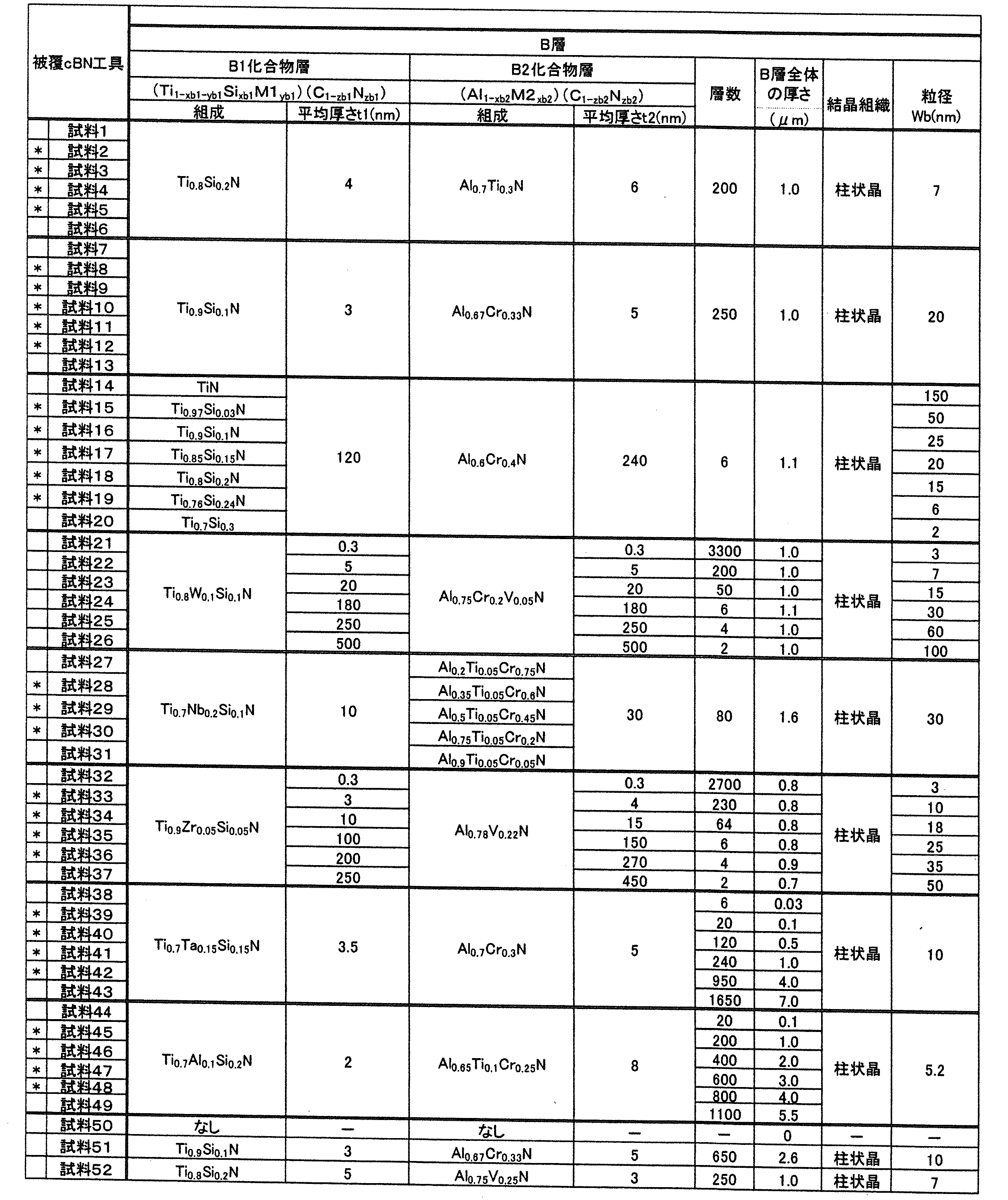
cBN焼結体Dを用い、試料1と同様にして基材を得、成膜条件を適宜調整して、表2および3に示す構成のD層およびB層をこの順で該基材上に積層した。 <Production of Samples 7 to 13>
Using cBN sintered body D, a base material was obtained in the same manner as in sample 1, and the film formation conditions were adjusted as appropriate. The layers D and B having the structures shown in Tables 2 and 3 were placed on the base material in this order. Laminated.
試料7では、厚さ方向(基材側から被膜表面へ向かう方向)にCおよびNの組成がステップ状または傾斜状に変化するTi0.9Si0.1CN層を含むA層を、B層の上に積層した。表2中、当該A層の組成を、便宜上「Ti0.9Si0.1CN*」と記している。当該A層の具体的な構成を表4に示す。また、当該A層は次のようにして形成した。 (Sample 7: Formation of layer A: Ti 0.9 Si 0.1 CN * )
In Sample 7, an A layer including a Ti 0.9 Si 0.1 CN layer in which the composition of C and N changes in a stepped or inclined manner in the thickness direction (direction from the substrate side toward the coating surface) is formed on the B layer. Laminated. In Table 2, the composition of the A layer is described as “Ti 0.9 Si 0.1 CN * ” for convenience. Table 4 shows a specific configuration of the A layer. The A layer was formed as follows.
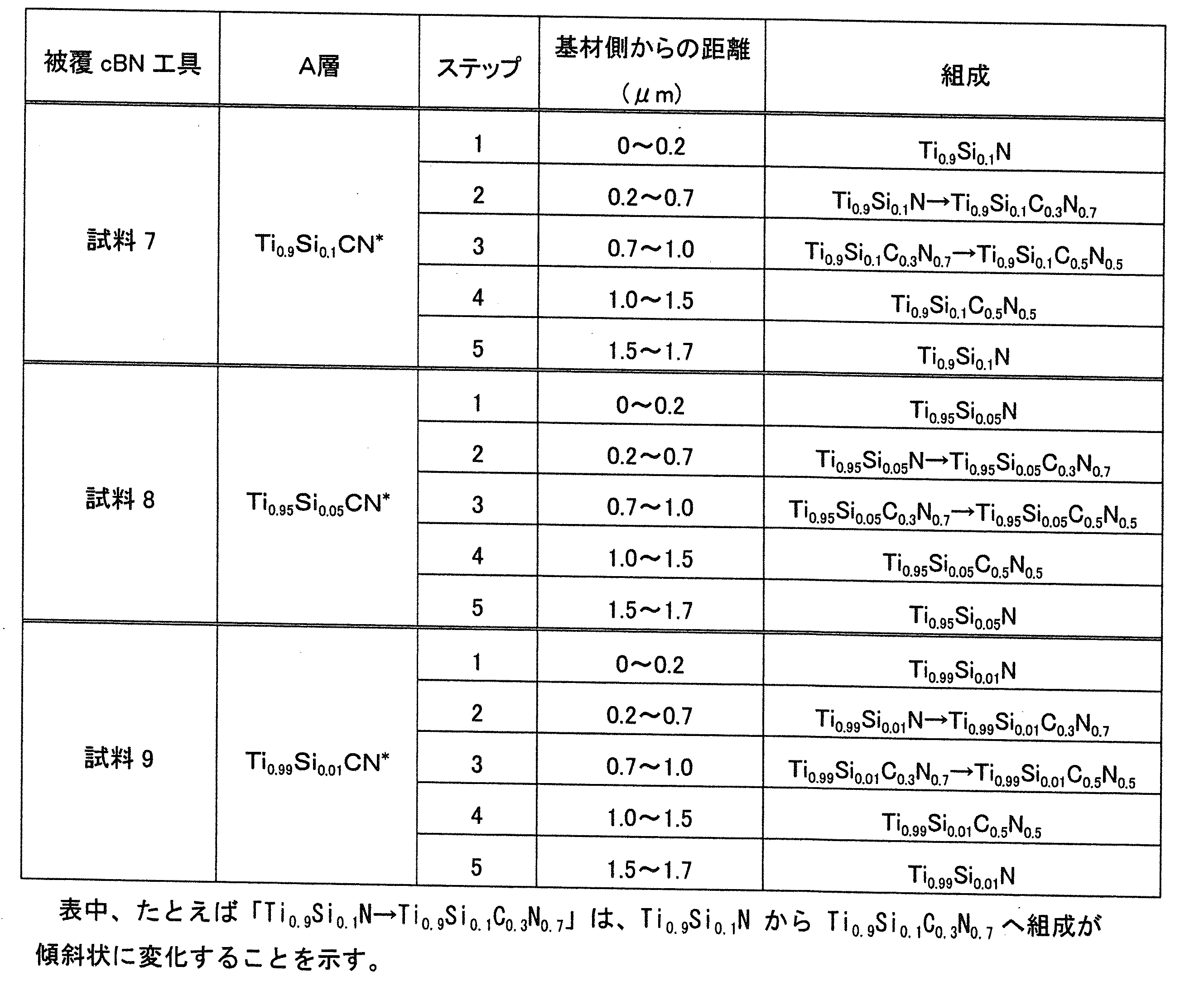
試料8では、厚さ方向(基材側から被膜表面へ向かう方向)にCおよびNの組成がステップ状または傾斜状に変化するTi0.95Si0.05CN層を含むA層を、B層の上に積層した。表2中、当該A層の組成を、便宜上「Ti0.95Si0.05CN*」と記している。当該A層の具体的な構成を表4に示す。また、当該A層は上記試料7のA層の形成において、A層の金属元素の組成をTi:Si=0.9:0.1からTi:Si=0.95:0.05とする以外は、試料7のA層と同様にして形成した。 (Sample 8: Formation of layer A: Ti 0.95 Si 0.05 CN * )
In sample 8, an A layer including a Ti 0.95 Si 0.05 CN layer in which the composition of C and N changes in a stepped or inclined manner in the thickness direction (direction from the substrate side toward the coating surface) is formed on the B layer. Laminated. In Table 2, the composition of the A layer is described as “Ti 0.95 Si 0.05 CN * ” for convenience. Table 4 shows a specific configuration of the A layer. In addition, in the formation of the A layer of the sample 7, the A layer has a composition other than changing the composition of the metal element of the A layer from Ti: Si = 0.9: 0.1 to Ti: Si = 0.95: 0.05. Was formed in the same manner as the A layer of Sample 7.
試料9では、厚さ方向(基材側から被膜表面へ向かう方向)にCおよびNの組成がステップ状または傾斜状に変化するTi0.99Si0.01CN層を含むA層を、B層の上に積層した。表2中、当該A層の組成を、便宜上「Ti0.99Si0.01CN*」と記している。当該A層の具体的な構成を表4に示す。また、当該A層は上記試料7のA層の形成において、A層の金属元素の組成をTi:Si=0.9:0.1からTi:Si=0.99:0.01とする以外は、試料7のA層と同様にして形成した。 (Sample 9: Formation of A layer: Ti 0.99 Si 0.01 CN *)
In sample 9, an A layer including a Ti 0.99 Si 0.01 CN layer in which the composition of C and N changes in a stepped or inclined manner in the thickness direction (from the substrate side toward the coating surface) is formed on the B layer. Laminated. In Table 2, the composition of the A layer is described as “Ti 0.99 Si 0.01 CN * ” for convenience. Table 4 shows a specific configuration of the A layer. In addition, in the formation of the A layer of the sample 7, the A layer has a composition other than changing the metal element composition of the A layer from Ti: Si = 0.9: 0.1 to Ti: Si = 0.99: 0.01. Was formed in the same manner as the A layer of Sample 7.
試料10~13では、厚さ方向(基材側から被膜表面へ向かう方向)にCおよびNの組成がステップ状または傾斜状に変化するTiCN層を含むA層を、B層の上に積層した。表2中、当該A層の組成を、便宜上「TiCN*1」と記している。当該A層の具体的な構成を表5に示す。また、当該A層は上記試料7のA層の形成において、A層の金属元素の組成をTiのみとし、A層形成時の基材の加熱温度を変化させる以外は、試料7のA層と同様にして形成した。ここで、基材の加熱温度は試料10においては試料7と同様に500℃とし、試料11は600℃、試料12は650℃、試料13では700℃とした。 (
In

cBN焼結体Bを用い、試料1と同様にして基材を得、成膜条件を適宜調整して、表2に示す構成のD層を該基材上に形成した。 <Manufacture of sample 14>
A cBN sintered body B was used to obtain a base material in the same manner as in Sample 1, and the film formation conditions were adjusted as appropriate to form a D layer having the structure shown in Table 2 on the base material.
続いて、次に示す条件で、B1化合物層とB2化合物層とを交互に3回ずつ繰り返して形成することにより、合計層数が6層であり、合計厚さ1.1μmのB層を、D層の上に積層した。 (Formation of layer B)
Subsequently, by repeatedly forming the B1 compound layer and the B2 compound layer three times under the following conditions, the total number of layers is 6, and the B layer having a total thickness of 1.1 μm is obtained. It was laminated on the D layer.
B1化合物層は次に示す条件で、蒸着時間を調整することにより、1層の厚さが120nmとなるように形成した
ターゲット :Ti
導入ガス :N2
成膜圧力 :3.5Pa
アーク放電電流 :140A
基板バイアス電圧:-35V。 (Formation of B1 compound layer)
The B1 compound layer was formed so that the thickness of one layer would be 120 nm by adjusting the deposition time under the following conditions: Target: Ti
Introduced gas: N 2
Deposition pressure: 3.5Pa
Arc discharge current: 140 A
Substrate bias voltage: -35V.
B2化合物層は次に示す条件で、蒸着時間を調整することにより、1層の厚さが240nmとなるように形成した
ターゲット :Al(60原子%)、Cr(40原子%)
導入ガス :N2
成膜圧力 :3.5Pa
アーク放電電流 :140A
基板バイアス電圧:-60V。 (Formation of B2 compound layer)
The B2 compound layer was formed so that the thickness of one layer was 240 nm by adjusting the deposition time under the following conditions: Target: Al (60 atomic%), Cr (40 atomic%)
Introduced gas: N 2
Deposition pressure: 3.5Pa
Arc discharge current: 140 A
Substrate bias voltage: -60V.
B層を形成した後、次の条件で、蒸着時間を調整することにより、厚さ0.02μmのC層をB層の上に積層した
ターゲット :Ti
導入ガス :N2
成膜圧力 :0.5Pa
アーク放電電流 :150A
基板バイアス電圧:-500V。 (Formation of C layer)
After forming the B layer, a 0.02 μm thick C layer was laminated on the B layer by adjusting the deposition time under the following conditions: Target: Ti
Introduced gas: N 2
Deposition pressure: 0.5 Pa
Arc discharge current: 150 A
Substrate bias voltage: -500V.
さらに、成膜条件を適宜調整して、表2に示す構成のA層をC層の上に積層し、被膜を形成した。これにより、試料14に係る被覆cBN工具を得た。 (Formation of layer A)
Further, the film formation conditions were adjusted as appropriate, and the A layer having the configuration shown in Table 2 was laminated on the C layer to form a coating. As a result, a coated cBN tool according to Sample 14 was obtained.
B1化合物層を形成する際のターゲットを表3に示す金属元素に変更する以外は、試料14と同様にして、試料15~20に係る被覆cBN工具を得た。 <Manufacture of samples 15 to 20>
Coated cBN tools according to Samples 15 to 20 were obtained in the same manner as Sample 14, except that the target for forming the B1 compound layer was changed to the metal element shown in Table 3.
cBN焼結体Cを用い、試料1と同様にして基材を得、成膜条件を適宜調整して、表2および3に示す構成のD層、B層およびA層をこの順で該基材上に積層し、被膜を形成することにより、試料21~26に係る被覆cBN工具を得た。なおこの際B層は、試料21~23では試料1と同様の方法で形成し、試料24~26では試料14と同様の方法で形成した。 <Manufacture of samples 21 to 26>
Using the cBN sintered body C, a base material was obtained in the same manner as in Sample 1, the film formation conditions were adjusted as appropriate, and the D layer, B layer, and A layer having the structures shown in Tables 2 and 3 were added in this order. The coated cBN tools according to Samples 21 to 26 were obtained by laminating on the material and forming a film. At this time, the layer B was formed by the same method as that of the sample 1 for the samples 21 to 23 and by the same method as that of the sample 14 for the samples 24 to 26.
cBN焼結体Eを用い、試料1と同様にして基材を得、成膜条件を適宜調整して、表2および3に示す構成のD層、B層をこの順で該基材上に積層した。なおこの際B層は、試料1と同様の方法で形成した。 <Manufacture of samples 27 to 31>
Using cBN sintered body E, a base material was obtained in the same manner as in sample 1, and the film formation conditions were adjusted as appropriate. The layers D and B having the structures shown in Tables 2 and 3 were placed on the base material in this order. Laminated. At this time, the B layer was formed by the same method as Sample 1.
試料27~31では、厚さ方向にCおよびNの組成がステップ状に変化するTiCN層を含むA層を、B層の上に積層した。表2中、当該A層の組成を、便宜上「TiCN*2」と記している。当該A層の具体的な構成を表5に示す。表5に示すように、当該A層は、基材側(cBN焼結体側)から、所定厚さ(ステップ)毎に、段階的に導入ガスの組成を変更して形成した。これによりB層の上に、厚さ方向にCおよびNの組成がステップ状に変化するTiCN層を含むA層が積層されてなる被膜を得た。そしてこれにより、試料27~31に係る被覆cBN工具を得た。 (Formation of layer A: TiCN * 2 )
In Samples 27 to 31, an A layer including a TiCN layer in which the composition of C and N changes stepwise in the thickness direction is laminated on the B layer. In Table 2, the composition of the A layer is described as “TiCN * 2 ” for convenience. Table 5 shows a specific configuration of the A layer. As shown in Table 5, the A layer was formed by changing the composition of the introduced gas stepwise from the base material side (cBN sintered body side) for each predetermined thickness (step). As a result, a film was obtained in which an A layer including a TiCN layer in which the composition of C and N changes stepwise in the thickness direction on the B layer. Thus, coated cBN tools according to Samples 27 to 31 were obtained.
cBN焼結体Fを用い、試料1と同様にして基材を得、成膜条件を適宜調整して、表2および3に示す構成のD層、B層、C層およびA層をこの順で該基材上に積層し、被膜を形成することにより、試料32~37に係る被覆cBN工具を得た。なおB層は、試料32~34では試料1と同様の方法で形成し、試料35~37では試料14と同様の方法で形成した。 <Manufacture of samples 32-37>
Using cBN sintered body F, a base material was obtained in the same manner as in sample 1, the film forming conditions were adjusted as appropriate, and the layers D, B, C, and A having the configurations shown in Tables 2 and 3 were arranged in this order. The coated cBN tools according to Samples 32-37 were obtained by laminating on the base material and forming a film. The layer B was formed by the same method as the sample 1 for the
cBN焼結体Gを用い、試料1と同様にして基材を得、成膜条件を適宜調整して、表2および3に示す構成のD層、B層およびA層をこの順で該基材上に積層し、被膜を形成することにより、試料38~43に係る被覆cBN工具を得た。なおB層は、試料1と同様の方法で形成した。 <Manufacture of samples 38 to 43>
Using the cBN sintered body G, a base material was obtained in the same manner as in Sample 1, the film formation conditions were adjusted as appropriate, and the D layer, B layer, and A layer having the structures shown in Tables 2 and 3 were added in this order. The coated cBN tools according to Samples 38 to 43 were obtained by laminating on the material and forming a film. The B layer was formed by the same method as Sample 1.
cBN焼結体Hを用い、試料1と同様にして基材を得、成膜条件を適宜調整して、表2および3に示す構成のD層、B層をこの順で該基材上に積層した。なお、この際B層は、試料1と同様の方法で形成した。 <Production of 44 to 49>
Using the cBN sintered body H, a base material was obtained in the same manner as in the sample 1, and the film formation conditions were adjusted as appropriate. The layers D and B having the configurations shown in Tables 2 and 3 were placed on the base material in this order. Laminated. At this time, the B layer was formed by the same method as Sample 1.
試料46~49では、厚さ方向にCおよびNの組成がステップ状または傾斜状に変化するTiCN層を含むA層を、B層の上に積層した。表2中、当該A層の組成を、便宜上「TiCN*3」と記している。当該A層の具体的な構成を表5に示す。表5に示すように、当該A層は、基材側(cBN焼結体側)から、傾斜状に導入ガスの組成を変化させた後、ステップ状に導入ガスの組成を変更して形成した。 (Formation of layer A: TiCN * 3 )
In Samples 46 to 49, an A layer including a TiCN layer in which the composition of C and N changes stepwise or in the thickness direction in the thickness direction was laminated on the B layer. In Table 2, the composition of the A layer is described as “TiCN * 3 ” for convenience. Table 5 shows a specific configuration of the A layer. As shown in Table 5, the A layer was formed by changing the composition of the introduced gas in a step shape after changing the composition of the introduced gas in an inclined manner from the base material side (cBN sintered body side).
cBN焼結体Dを用い、試料1と同様にして基材を得、成膜条件を適宜調整して、表2に示す構成のA層を該基材上に形成することにより、試料50に係る被覆cBN工具を得た。 <Manufacture of
Using cBN sintered body D, a base material was obtained in the same manner as in sample 1, and film formation conditions were adjusted as appropriate, and an A layer having the structure shown in Table 2 was formed on the base material. Such a coated cBN tool was obtained.
cBN焼結体Dを用い、試料1と同様にして基材を得、成膜条件を適宜調整して、表2および3に示す構成のD層、B層をこの順で該基材上に形成することにより、試料51に係る被覆cBN工具を得た。なおB層は試料1と同様の方法で形成した。 <Manufacture of sample 51>
Using cBN sintered body D, a base material was obtained in the same manner as in sample 1, and the film formation conditions were adjusted as appropriate, so that the D layer and B layer having the configurations shown in Tables 2 and 3 were placed on the base material in this order By forming, a coated cBN tool according to sample 51 was obtained. The B layer was formed by the same method as Sample 1.
cBN焼結体Dを用い、試料1と同様にして基材を得、成膜条件を適宜調整して、表2および3に示す構成のD層、B層およびA層をこの順で該基材上に形成することにより、試料52に係る被覆cBN工具を得た。なおB層は試料1と同様の方法で形成した。 <Manufacture of sample 52>
Using cBN sintered body D, a base material was obtained in the same manner as in sample 1, the film formation conditions were adjusted as appropriate, and the D layer, B layer, and A layer having the structures shown in Tables 2 and 3 were added in this order. By forming on the material, a coated cBN tool according to sample 52 was obtained. The B layer was formed by the same method as Sample 1.
以上のようにして得られた試料1~52に係る被覆cBN工具の切削性能および面粗度寿命を、焼入鋼の高速連続切削により評価した。 << Evaluation >>
The cutting performance and surface roughness life of the coated cBN tools according to Samples 1 to 52 obtained as described above were evaluated by high-speed continuous cutting of hardened steel.
各試料を切断し、被膜の断面をTEMで観察することにより、A層、B層およびC層に含まれる結晶粒の形状を確認した。そして前述の方法に従って、粒径Wa、WbおよびWcを計測した。その結果を表2および3に示す。 <Measurement of particle size>
Each sample was cut, and the cross section of the film was observed with a TEM to confirm the shape of the crystal grains contained in the A layer, the B layer, and the C layer. And according to the above-mentioned method, particle size Wa, Wb, and Wc was measured. The results are shown in Tables 2 and 3.
各試料の工具を用い、次に示す切削条件に従って、切削距離4kmの切削加工を行なった。そして、光学顕微鏡を使用して工具の逃げ面摩耗量VBを測定した。また、「JIS B 0601」に準拠して、加工後の被削材の「十点平均粗さ(μm)」(すなわち、Rzjis)を測定し、面粗度Rzとした。結果を表6に示す。表6中、逃げ面摩耗量VBが小さいほど、耐逃げ面摩耗性に優れる。また、Rzが小さいほど耐境界摩耗性に優れ、高精度加工が可能であることを示している。 <Measurement of flank wear amount VB and surface roughness Rz>
Using the tool of each sample, cutting with a cutting distance of 4 km was performed according to the following cutting conditions. The flank wear amount VB of the tool was measured using an optical microscope. Further, in accordance with “JIS B 0601”, the “ten-point average roughness (μm)” (that is, Rzjis) of the work material after the machining was measured to obtain the surface roughness Rz. The results are shown in Table 6. In Table 6, the smaller the flank wear amount VB, the better the flank wear resistance. Further, it is shown that the smaller Rz is, the better the boundary wear resistance is, and the high precision machining is possible.
被削材 :SCM415H(HRC60)、外径φ30、ワーク1個当たりの切削距離が6.28mのもの
切削速度:200m/min
送り量 :f=0.1mm/rev
切込み :ap=0.1mm
切削油 :エマルジョン(商品名「システムカット96」、製造元「(株)日本フルードシステム」)を20倍希釈したもの(湿式切削)。 (Cutting conditions)
Work material: SCM415H (HRC60), outer diameter φ30, cutting distance per workpiece 6.28 m Cutting speed: 200 m / min
Feed amount: f = 0.1 mm / rev
Cutting depth: ap = 0.1mm
Cutting oil: A 20-fold diluted emulsion (trade name “System Cut 96”, manufacturer “Nihon Fluid System”) (wet cutting).
次に、寿命判定基準をRz=3.2μmとして、高精度加工における面粗度寿命を測定した。すなわち、上記の切削条件で繰り返し加工を行ない、ワーク1個の加工(切削距離:6.28m)が終了する度に表面粗さ計を使用して加工後ワークの面粗度Rzを測定し、Rzが3.2μmを超えた時点で試験終了とした。そして、6.28m×ワーク個数から総切削距離(km)を算出した。さらに、Rzを縦軸、切削距離を横軸とする散布図を作成し、該散布図上において終了点と終了直前の点との2点を結ぶ直線上で、Rzが3.2μmに達する切削距離を面粗度寿命と判定した。その結果を表6に示す。 <Measurement of surface roughness life>
Next, the surface roughness life in high-precision machining was measured with a life criterion of Rz = 3.2 μm. That is, the surface roughness Rz of the post-working workpiece is measured using a surface roughness meter every time one piece of workpiece (cutting distance: 6.28 m) is finished by repeatedly machining under the above cutting conditions, The test was terminated when Rz exceeded 3.2 μm. Then, the total cutting distance (km) was calculated from 6.28 m × the number of workpieces. Further, a scatter diagram is created with Rz as the vertical axis and the cutting distance as the horizontal axis. On the scatter diagram, the cutting where Rz reaches 3.2 μm on the straight line connecting the end point and the point just before the end. The distance was determined as the surface roughness life. The results are shown in Table 6.

表6中、左端列に「*」が付された試料が実施例に係る被覆cBN工具である。表1~6より明らかなように、上記構成(1)~(10)を備える実施例の被覆cBN工具は、かかる条件を満たさない工具に比し、耐逃げ面摩耗性および耐境界摩耗性に優れ、焼入鋼の高精度加工において優れた工具寿命を有することが確認された。 << Results and Discussion >>
In Table 6, the sample with “*” in the left end column is the coated cBN tool according to the example. As is clear from Tables 1 to 6, the coated cBN tool of the example having the above-described configurations (1) to (10) is more resistant to flank wear resistance and boundary wear resistance than a tool that does not satisfy such conditions. It has been confirmed that it has excellent tool life in high precision machining of hardened steel.
試料2~5および45~48の評価結果から、A層の厚さが1μm以上3μm以下である試料3、45および46は、特に優れた面粗度寿命を示す傾向が確認された。したがって、A層の厚さは1μm以上3μm以下であることが好ましい。 <Thickness of layer A>
From the evaluation results of Samples 2 to 5 and 45 to 48, it was confirmed that Samples 3, 45 and 46 in which the thickness of the A layer was 1 μm or more and 3 μm or less showed a particularly excellent surface roughness life. Therefore, the thickness of the A layer is preferably 1 μm or more and 3 μm or less.
試料8~12の評価では、A層を構成する柱状晶の粒径Waが50nm以上300nm以下である試料9~11は、かかる条件を満たさない試料8および12に比し優れた面粗度寿命を示す傾向が確認された。したがって、Waは50nm以上300nm以下であることが好ましい。 <The particle size Wa of the columnar crystals constituting the A layer>
In the evaluation of Samples 8 to 12, Samples 9 to 11 in which the grain size Wa of the columnar crystals constituting the A layer is 50 nm to 300 nm are superior to those of Samples 8 and 12 that do not satisfy such conditions. The tendency which shows was confirmed. Therefore, Wa is preferably 50 nm or more and 300 nm or less.
試料15~19の評価では、B層を構成する柱状晶の粒径Wbが7nm以上40nmである試料16~18は、かかる条件を満たさない試料15および19に比し優れた面粗度寿命を示す傾向が確認された。したがって、Wbは7nm以上40nm以下であることが好ましい。 <Particle size Wb of the columnar crystals constituting the B layer>
In the evaluation of Samples 15 to 19, Samples 16 to 18 in which the grain size Wb of the columnar crystals constituting the B layer is 7 nm or more and 40 nm have an excellent surface roughness life compared to Samples 15 and 19 that do not satisfy such conditions. The tendency to show was confirmed. Therefore, Wb is preferably 7 nm or more and 40 nm or less.
試料28~30の評価では、B2化合物層に含まれる(Al1-xb2M2xb2)(C1-zb2Nzb2)において、M2がTiおよびCrの少なくとも1つを表わし、M2の組成xb2が0.25以上0.5以下である試料29および30は、かかる条件を満たさない試料28に比し、優れた面粗度寿命を示した。したがって、M2の組成xb2は0.25以上0.5以下であることが好ましい。 <Composition of B2 compound layer>
In the evaluation of samples 28 to 30, in (Al 1 -xb2 M2 xb2 ) (C 1 -zb2 N zb2 ) included in the B2 compound layer, M2 represents at least one of Ti and Cr, and the composition xb2 of M2 is 0
試料22~25および試料33~36の評価では、B層が30nm未満の化合物層を含む場合(試料22、23、33、34)、面粗度寿命が向上する傾向が確認された。したがって、B層は一部または全部が30nm未満の層で構成されることが好ましい。 <B1 compound layer and B2 compound layer thickness>
In the evaluation of Samples 22 to 25 and Samples 33 to 36, it was confirmed that when the B layer includes a compound layer of less than 30 nm (Samples 22, 23, 33, and 34), the surface roughness life tends to be improved. Therefore, it is preferable that part or all of the B layer is composed of a layer having a thickness of less than 30 nm.
試料39~42の評価では、B層全体の厚さの範囲が0.1μm以上4μm以下であり、これらのうち該厚さが0.5μmである試料40と該厚さが1.0μmである試料41は特に優れた面粗度寿命を示した。したがって、B層全体の厚さは好ましくは0.1μm以上4μm以下であり、より好ましくは0.5μm以上4μm以下である。 <Total thickness of layer B>
In the evaluation of the samples 39 to 42, the thickness range of the entire B layer is 0.1 μm or more and 4 μm or less. Among these, the
Claims (18)
- 少なくとも切れ刃部分が立方晶窒化硼素焼結体と該立方晶窒化硼素焼結体の表面上に形成された被膜とを備える表面被覆窒化硼素焼結体工具であって、
前記立方晶窒化硼素焼結体は、立方晶窒化硼素粒子を30体積%以上80体積%以下含み、周期表の第4族元素、第5族元素および第6族元素の窒化物、炭化物、硼化物、酸化物ならびにこれらの固溶体からなる群の中から選択された少なくとも1種の化合物とアルミニウム化合物と不可避不純物とを含む結合相をさらに含み、
前記被膜はA層とB層とを備え、
前記A層は柱状晶から構成され、MLaza1(Mは周期表の第4族元素、第5族元素および第6族元素、AlならびにSiの1種以上を表わし、LaはB、C、NおよびOの1種以上を表わし、za1は0.85以上1.0以下である)を含み、
前記B層は柱状晶から構成され、組成の異なる2種以上の化合物層が交互にそれぞれ1つ以上積層されてなり、
前記化合物層のそれぞれの厚さは、0.5nm以上300nm以下であり、
前記化合物層の1種であるB1化合物層は、(Ti1-xb1-yb1Sixb1M1yb1)(C1-zb1Nzb1)(M1はTiを除く周期表の第4族元素、第5族元素および第6族元素ならびにAlの1種以上を表わし、xb1は0.01以上0.25以下であり、yb1は0以上0.7以下であり、zb1は0.4以上1以下である)を含み、
前記化合物層の1種であって前記B1化合物層とは異なるB2化合物層は、(Al1-xb2M2xb2)(C1-zb2Nzb2)(M2は周期表の第4族元素、第5族元素および第6族元素ならびにSiの1種以上を表わし、xb2は0.2以上0.7以下であり、zb2は0.4以上1以下である)を含み、
前記A層の厚さは0.2μm以上10μm以下であり、前記B層の厚さは0.05μm以上5μm以下であり、かつ前記被膜全体の厚さは0.3μm以上15μm以下であり、
前記A層に含まれる柱状晶の粒径Waは10nm以上400nm以下であり、かつ前記B層に含まれる柱状晶の粒径Wbは5nm以上70nm以下である、表面被覆窒化硼素焼結体工具。 A surface-coated boron nitride sintered body tool comprising at least a cutting edge portion comprising a cubic boron nitride sintered body and a coating formed on the surface of the cubic boron nitride sintered body,
The cubic boron nitride sintered body contains 30% by volume or more and 80% by volume or less of cubic boron nitride particles, and includes nitrides, carbides, borons of Group 4 elements, Group 5 elements and Group 6 elements of the periodic table. A binder phase comprising at least one compound selected from the group consisting of a compound, an oxide, and a solid solution thereof, an aluminum compound, and inevitable impurities;
The coating comprises an A layer and a B layer,
The A layer is composed of columnar crystals, and MLa za1 (M represents one or more of Group 4 element, Group 5 element and Group 6 element, Al and Si in the periodic table, and La represents B, C, N And one or more of O and za1 is 0.85 or more and 1.0 or less),
The B layer is composed of columnar crystals, and two or more kinds of compound layers having different compositions are alternately laminated, respectively.
Each thickness of the compound layer is 0.5 nm or more and 300 nm or less,
The B1 compound layer, which is one of the compound layers, is composed of (Ti 1 -xb1-yb1 Si xb1 M1 yb1 ) (C 1 -zb1 N zb1 ), where M1 is a Group 4 element or Group 5 in the periodic table excluding Ti. And represents at least one of element, group 6 element and Al, xb1 is 0.01 or more and 0.25 or less, yb1 is 0 or more and 0.7 or less, and zb1 is 0.4 or more and 1 or less) Including
The B2 compound layer, which is one of the compound layers and is different from the B1 compound layer, is (Al 1 -xb2 M2 xb2 ) (C 1 -zb2 N zb2 ) (M2 is a group 4 element of the periodic table, A group element, a Group 6 element, and one or more of Si, xb2 is 0.2 or more and 0.7 or less, and zb2 is 0.4 or more and 1 or less.
The thickness of the A layer is 0.2 μm or more and 10 μm or less, the thickness of the B layer is 0.05 μm or more and 5 μm or less, and the total thickness of the coating is 0.3 μm or more and 15 μm or less,
The surface-coated boron nitride sintered body tool, wherein the grain size Wa of the columnar crystals contained in the A layer is 10 nm or more and 400 nm or less, and the grain diameter Wb of the columnar crystals contained in the B layer is 5 nm or more and 70 nm or less. - 前記A層は、(Ti1-xaMaxa)(C1-za2Nza2)(MaはTiを除く周期表の第4族元素、第5族元素および第6族元素、AlならびにSiの1種以上を表わし、xaは0以上0.7以下であり、za2は0以上1以下である)を含む、請求項1に記載の表面被覆窒化硼素焼結体工具。 The A layer, (Ti 1-xa Ma xa ) (C 1-za2 N za2) (Ma fourth group elements of the periodic table excluding Ti, the group 5 element and a group 6 element, Al and Si 1 2. The surface-coated boron nitride sintered body tool according to claim 1, wherein the surface-coated boron nitride sintered body tool includes a seed or more, xa is 0 or more and 0.7 or less, and za2 is 0 or more and 1 or less.
- 前記A層では、Nの組成za2が、前記立方晶窒化硼素焼結体側から当該A層の表面側へ向かってステップ状または傾斜状に変化する、請求項2に記載の表面被覆窒化硼素焼結体工具。 3. The surface-coated boron nitride sintered body according to claim 2, wherein in the A layer, the composition za <b> 2 of N changes in a stepped or inclined manner from the cubic boron nitride sintered body side toward the surface side of the A layer. Body tool.
- 前記A層は、当該A層の表面側に、前記立方晶窒化硼素焼結体側よりもCの組成の大きな領域を有する、請求項2または請求項3に記載の表面被覆窒化硼素焼結体工具。 The surface-coated boron nitride sintered body tool according to claim 2 or 3, wherein the A layer has a region having a larger C composition than the cubic boron nitride sintered body side on the surface side of the A layer. .
- 前記B2化合物層において、前記M2はTiおよびCrの少なくとも1つを表わし、前記M2の組成xb2は0.25以上0.5以下である、請求項1~請求項4のいずれか1項に記載の表面被覆窒化硼素焼結体工具。 In the B2 compound layer, the M2 represents at least one of Ti and Cr, and the composition xb2 of the M2 is 0.25 or more and 0.5 or less, according to any one of claims 1 to 4. Surface coated boron nitride sintered body tool.
- 前記粒径Waは50nm以上300nm以下である、請求項1~請求項5のいずれか1項に記載の表面被覆窒化硼素焼結体工具。 The surface-coated boron nitride sintered body tool according to any one of claims 1 to 5, wherein the particle diameter Wa is 50 nm or more and 300 nm or less.
- 前記粒径Wbは7nm以上40nm以下である、請求項1~請求項6のいずれか1項に記載の表面被覆窒化硼素焼結体工具。 The surface-coated boron nitride sintered body tool according to any one of claims 1 to 6, wherein the particle diameter Wb is 7 nm or more and 40 nm or less.
- 前記粒径Waと前記粒径Wbとが、1<Wa/Wb≦30の関係を満たす、請求項1~請求項7のいずれか1項に記載の表面被覆窒化硼素焼結体工具。 The surface-coated boron nitride sintered body tool according to any one of claims 1 to 7, wherein the particle diameter Wa and the particle diameter Wb satisfy a relationship of 1 <Wa / Wb ≦ 30.
- 前記A層は前記B層よりも前記被膜の表面側に設けられている、請求項1~請求項8のいずれか1項に記載の表面被覆窒化硼素焼結体工具。 The surface-coated boron nitride sintered body tool according to any one of claims 1 to 8, wherein the A layer is provided closer to the surface of the coating than the B layer.
- 前記被膜は、前記A層と前記B層との間に設けられたC層をさらに含み、
前記C層は、McLczc(Mcは周期表の第4族元素、第5族元素および第6族元素、AlならびにSiの1種以上を表わし、LcはB、C、NおよびOの1種以上を表わし、zcは0以上0.85以下である)を含み、
前記C層の厚さは0.005μm以上0.5μm以下である、請求項1~請求項9のいずれか1項に記載の表面被覆窒化硼素焼結体工具。 The coating further includes a C layer provided between the A layer and the B layer,
The C layer is McLc zc (Mc represents one or more of Group 4 element, Group 5 element and Group 6 element of the periodic table, Al and Si, and Lc represents one of B, C, N and O) And zc is 0 or more and 0.85 or less),
The surface-coated boron nitride sintered body tool according to any one of claims 1 to 9, wherein a thickness of the C layer is 0.005 µm or more and 0.5 µm or less. - 前記Lcの組成zcは0よりも大きく0.7未満である、請求項10に記載の表面被覆窒化硼素焼結体工具。 The surface-coated boron nitride sintered body tool according to claim 10, wherein the composition zc of Lc is greater than 0 and less than 0.7.
- 前記C層は、前記A層および前記B層を構成する元素の少なくとも1種以上を含む、請求項10または請求項11に記載の表面被覆窒化硼素焼結体工具。 The surface-coated boron nitride sintered body tool according to claim 10 or 11, wherein the C layer includes at least one element constituting the A layer and the B layer.
- 前記C層は粒状晶から構成され、当該粒状晶の粒径Wcは5nm以上300nm以下である、請求項10~請求項12のいずれか1項に記載の表面被覆窒化硼素焼結体工具。 The surface-coated boron nitride sintered body tool according to any one of claims 10 to 12, wherein the C layer is composed of granular crystals, and the particle diameter Wc of the granular crystals is 5 nm or more and 300 nm or less.
- 前記被膜は、前記立方晶窒化硼素焼結体と前記B層との間に設けられたD層をさらに含み、
前記D層は、MdLdzd(Mdは周期表の第4族元素、第5族元素および第6族元素、AlならびにSiの1種以上を表わし、LdはB、C、NおよびOの1種以上を表わし、zdは0.85以上1.0以下である)を含む、請求項1~請求項13のいずれか1項に記載の表面被覆窒化硼素焼結体工具。 The coating further includes a D layer provided between the cubic boron nitride sintered body and the B layer,
The D layer is MdLd zd (Md represents one or more of Group 4 element, Group 5 element and Group 6 element of the periodic table, Al and Si, and Ld represents one of B, C, N and O) The surface-coated boron nitride sintered body tool according to any one of claims 1 to 13, including the above, wherein zd is not less than 0.85 and not more than 1.0. - 前記立方晶窒化硼素焼結体は、前記立方晶窒化硼素粒子を50体積%以上65体積%以下含む、請求項1~請求項14のいずれか1項に記載の表面被覆窒化硼素焼結体工具。 The surface-coated boron nitride sintered body tool according to any one of claims 1 to 14, wherein the cubic boron nitride sintered body contains the cubic boron nitride particles in an amount of 50% by volume to 65% by volume. .
- 前記立方晶窒化硼素焼結体と前記被膜との界面では、前記立方晶窒化硼素粒子が前記結合相よりも前記被膜側に突出した形状を有し、
前記立方晶窒化硼素粒子と前記結合相との段差が0.05μm以上1.0μm以下である、請求項1~請求項15のいずれか1項に記載の表面被覆窒化硼素焼結体工具。 At the interface between the cubic boron nitride sintered body and the coating, the cubic boron nitride particles have a shape protruding to the coating side from the binder phase,
The surface-coated boron nitride sintered body tool according to any one of claims 1 to 15, wherein a step between the cubic boron nitride particles and the binder phase is 0.05 µm or more and 1.0 µm or less. - 前記立方晶窒化硼素粒子の体積含有率は、前記立方晶窒化硼素焼結体と前記被膜との界面から前記立方晶窒化硼素焼結体の内部に向かって高くなる、請求項1~請求項16のいずれか1項に記載の表面被覆窒化硼素焼結体工具。 The volume content of the cubic boron nitride particles increases from the interface between the cubic boron nitride sintered body and the coating toward the inside of the cubic boron nitride sintered body. The surface-coated boron nitride sintered body tool according to any one of the above.
- 前記立方晶窒化硼素粒子の粒径は、前記立方晶窒化硼素焼結体と前記被膜との界面から前記立方晶窒化硼素焼結体の内部に向かって大きくなる、請求項1~請求項17のいずれか1項に記載の表面被覆窒化硼素焼結体工具。 The particle diameter of the cubic boron nitride particles increases from the interface between the cubic boron nitride sintered body and the coating toward the inside of the cubic boron nitride sintered body. The surface-coated boron nitride sintered body tool according to any one of claims 1 to 4.
Priority Applications (6)
| Application Number | Priority Date | Filing Date | Title |
|---|---|---|---|
| CA2913626A CA2913626A1 (en) | 2013-07-03 | 2014-06-05 | Surface-coated boron nitride sintered body tool |
| EP14819914.4A EP3023180B1 (en) | 2013-07-03 | 2014-06-05 | Surface-coated boron nitride sintered body tool |
| CN201480031258.6A CN105263657B (en) | 2013-07-03 | 2014-06-05 | The coating boron nitride sintered body instrument in surface |
| US14/892,542 US9850177B2 (en) | 2013-07-03 | 2014-06-05 | Surface-coated boron nitride sintered body tool |
| KR1020157033668A KR20160028412A (en) | 2013-07-03 | 2014-06-05 | Surface-coated boron nitride sintered tool |
| PL14819914.4T PL3023180T3 (en) | 2013-07-03 | 2014-06-05 | Surface-coated boron nitride sintered body tool |
Applications Claiming Priority (2)
| Application Number | Priority Date | Filing Date | Title |
|---|---|---|---|
| JP2013139797A JP5663814B2 (en) | 2013-07-03 | 2013-07-03 | Surface coated boron nitride sintered body tool |
| JP2013-139797 | 2013-07-03 |
Publications (1)
| Publication Number | Publication Date |
|---|---|
| WO2015001903A1 true WO2015001903A1 (en) | 2015-01-08 |
Family
ID=52143489
Family Applications (1)
| Application Number | Title | Priority Date | Filing Date |
|---|---|---|---|
| PCT/JP2014/064957 WO2015001903A1 (en) | 2013-07-03 | 2014-06-05 | Surface-coated boron nitride sintered tool |
Country Status (8)
| Country | Link |
|---|---|
| US (1) | US9850177B2 (en) |
| EP (1) | EP3023180B1 (en) |
| JP (1) | JP5663814B2 (en) |
| KR (1) | KR20160028412A (en) |
| CN (1) | CN105263657B (en) |
| CA (1) | CA2913626A1 (en) |
| PL (1) | PL3023180T3 (en) |
| WO (1) | WO2015001903A1 (en) |
Families Citing this family (3)
| Publication number | Priority date | Publication date | Assignee | Title |
|---|---|---|---|---|
| JP5742042B2 (en) | 2013-10-31 | 2015-07-01 | 住友電工ハードメタル株式会社 | Surface coated boron nitride sintered body tool |
| JP6958614B2 (en) * | 2017-05-23 | 2021-11-02 | 住友電気工業株式会社 | Coating and cutting tools |
| JP7277820B2 (en) * | 2019-03-18 | 2023-05-19 | 株式会社Moldino | coated cutting tools |
Citations (6)
| Publication number | Priority date | Publication date | Assignee | Title |
|---|---|---|---|---|
| JP2008188689A (en) | 2007-02-01 | 2008-08-21 | Sumitomo Electric Hardmetal Corp | Surface coated cutting tool |
| JP2008534297A (en) | 2005-04-01 | 2008-08-28 | エーリコン・トレイディング・アーゲー・トリューバッハ | Multilayer hard material coating for tools |
| JP2008254159A (en) * | 2007-04-09 | 2008-10-23 | Mitsubishi Materials Corp | Surface-coated cutting tool made of cubic boron nitride group ultrahigh-pressure sintered material |
| WO2010150335A1 (en) | 2009-06-22 | 2010-12-29 | 株式会社タンガロイ | Tool having coated cubic boron nitride sintered body |
| WO2011129422A1 (en) * | 2010-04-16 | 2011-10-20 | 株式会社タンガロイ | Coated sintered cbn |
| WO2012005275A1 (en) | 2010-07-06 | 2012-01-12 | 株式会社タンガロイ | Coated polycrystalline cbn tool |
Family Cites Families (11)
| Publication number | Priority date | Publication date | Assignee | Title |
|---|---|---|---|---|
| US4311490A (en) * | 1980-12-22 | 1982-01-19 | General Electric Company | Diamond and cubic boron nitride abrasive compacts using size selective abrasive particle layers |
| US5330853A (en) * | 1991-03-16 | 1994-07-19 | Leybold Ag | Multilayer Ti-Al-N coating for tools |
| JPH08206902A (en) * | 1994-12-01 | 1996-08-13 | Sumitomo Electric Ind Ltd | Sintered body tip for cutting and its manufacture |
| AU7729900A (en) * | 1999-11-12 | 2001-05-30 | Kerr Corporation | Adherent hard coatings for dental burs and other applications |
| US20080160338A1 (en) | 2004-03-29 | 2008-07-03 | Kyocera Corporation | Surface Coated Member and Cutting Tool |
| WO2007111301A1 (en) | 2006-03-28 | 2007-10-04 | Kyocera Corporation | Surface-coated tool |
| JP5005262B2 (en) * | 2006-05-26 | 2012-08-22 | 三菱マテリアル株式会社 | Cutting tool made of surface-coated cubic boron nitride-based ultra-high pressure sintered material that exhibits excellent surface finish accuracy over a long period of time in high-speed cutting of hardened steel |
| BRPI0717566B1 (en) | 2006-09-26 | 2019-01-22 | Oerlikon Surface Solutions Ag Truebbach | hard coated workpiece, its manufacturing process, and method for fabricating device |
| JP5444709B2 (en) | 2008-12-24 | 2014-03-19 | 新日鐵住金株式会社 | Method for producing blast furnace coke |
| SE533883C2 (en) * | 2009-06-01 | 2011-02-22 | Seco Tools Ab | Nanolaminated coated cutting tool |
| JP5545646B2 (en) | 2010-06-18 | 2014-07-09 | ダイハツ工業株式会社 | Motor drive control device |
-
2013
- 2013-07-03 JP JP2013139797A patent/JP5663814B2/en active Active
-
2014
- 2014-06-05 US US14/892,542 patent/US9850177B2/en active Active
- 2014-06-05 EP EP14819914.4A patent/EP3023180B1/en active Active
- 2014-06-05 CA CA2913626A patent/CA2913626A1/en not_active Abandoned
- 2014-06-05 CN CN201480031258.6A patent/CN105263657B/en active Active
- 2014-06-05 WO PCT/JP2014/064957 patent/WO2015001903A1/en active Application Filing
- 2014-06-05 PL PL14819914.4T patent/PL3023180T3/en unknown
- 2014-06-05 KR KR1020157033668A patent/KR20160028412A/en not_active Application Discontinuation
Patent Citations (6)
| Publication number | Priority date | Publication date | Assignee | Title |
|---|---|---|---|---|
| JP2008534297A (en) | 2005-04-01 | 2008-08-28 | エーリコン・トレイディング・アーゲー・トリューバッハ | Multilayer hard material coating for tools |
| JP2008188689A (en) | 2007-02-01 | 2008-08-21 | Sumitomo Electric Hardmetal Corp | Surface coated cutting tool |
| JP2008254159A (en) * | 2007-04-09 | 2008-10-23 | Mitsubishi Materials Corp | Surface-coated cutting tool made of cubic boron nitride group ultrahigh-pressure sintered material |
| WO2010150335A1 (en) | 2009-06-22 | 2010-12-29 | 株式会社タンガロイ | Tool having coated cubic boron nitride sintered body |
| WO2011129422A1 (en) * | 2010-04-16 | 2011-10-20 | 株式会社タンガロイ | Coated sintered cbn |
| WO2012005275A1 (en) | 2010-07-06 | 2012-01-12 | 株式会社タンガロイ | Coated polycrystalline cbn tool |
Non-Patent Citations (1)
| Title |
|---|
| See also references of EP3023180A4 |
Also Published As
| Publication number | Publication date |
|---|---|
| EP3023180A1 (en) | 2016-05-25 |
| CA2913626A1 (en) | 2015-01-08 |
| US20160194254A1 (en) | 2016-07-07 |
| JP5663814B2 (en) | 2015-02-04 |
| KR20160028412A (en) | 2016-03-11 |
| EP3023180B1 (en) | 2022-08-31 |
| JP2015013323A (en) | 2015-01-22 |
| CN105263657B (en) | 2017-03-15 |
| US9850177B2 (en) | 2017-12-26 |
| EP3023180A4 (en) | 2017-03-01 |
| PL3023180T3 (en) | 2023-01-02 |
| CN105263657A (en) | 2016-01-20 |
Similar Documents
| Publication | Publication Date | Title |
|---|---|---|
| KR101635487B1 (en) | Cutting tool | |
| JP5742042B2 (en) | Surface coated boron nitride sintered body tool | |
| JP6016270B2 (en) | Surface coated boron nitride sintered body tool | |
| JP6355124B2 (en) | Surface coated boron nitride sintered body tool | |
| JP6016271B2 (en) | Surface coated boron nitride sintered body tool | |
| JP5663814B2 (en) | Surface coated boron nitride sintered body tool | |
| WO2018070195A1 (en) | Surface-coated cutting tool | |
| JP6016269B2 (en) | Surface coated boron nitride sintered body tool | |
| JP5663815B2 (en) | Surface coated boron nitride sintered body tool | |
| JP5663813B2 (en) | Surface coated boron nitride sintered body tool | |
| JP6253112B2 (en) | Surface coated boron nitride sintered body tool | |
| JP6198002B2 (en) | A surface-coated cutting tool that exhibits high wear resistance and chipping resistance with a hard coating layer in high-speed cutting. | |
| JP2010137336A (en) | Surface-coated cutting tool |
Legal Events
| Date | Code | Title | Description |
|---|---|---|---|
| WWE | Wipo information: entry into national phase |
Ref document number: 201480031258.6 Country of ref document: CN |
|
| 121 | Ep: the epo has been informed by wipo that ep was designated in this application |
Ref document number: 14819914 Country of ref document: EP Kind code of ref document: A1 |
|
| WWE | Wipo information: entry into national phase |
Ref document number: 14892542 Country of ref document: US |
|
| ENP | Entry into the national phase |
Ref document number: 2913626 Country of ref document: CA Ref document number: 20157033668 Country of ref document: KR Kind code of ref document: A |
|
| WWE | Wipo information: entry into national phase |
Ref document number: 2014819914 Country of ref document: EP |
|
| NENP | Non-entry into the national phase |
Ref country code: DE |