WO2014208499A1 - Resist underlayer film forming composition containing pyrrole novolac resin - Google Patents
Resist underlayer film forming composition containing pyrrole novolac resin Download PDFInfo
- Publication number
- WO2014208499A1 WO2014208499A1 PCT/JP2014/066560 JP2014066560W WO2014208499A1 WO 2014208499 A1 WO2014208499 A1 WO 2014208499A1 JP 2014066560 W JP2014066560 W JP 2014066560W WO 2014208499 A1 WO2014208499 A1 WO 2014208499A1
- Authority
- WO
- WIPO (PCT)
- Prior art keywords
- group
- carbon atoms
- underlayer film
- resist underlayer
- resist
- Prior art date
Links
- 0 C*[n]1cccc1 Chemical compound C*[n]1cccc1 0.000 description 1
Classifications
-
- G—PHYSICS
- G03—PHOTOGRAPHY; CINEMATOGRAPHY; ANALOGOUS TECHNIQUES USING WAVES OTHER THAN OPTICAL WAVES; ELECTROGRAPHY; HOLOGRAPHY
- G03F—PHOTOMECHANICAL PRODUCTION OF TEXTURED OR PATTERNED SURFACES, e.g. FOR PRINTING, FOR PROCESSING OF SEMICONDUCTOR DEVICES; MATERIALS THEREFOR; ORIGINALS THEREFOR; APPARATUS SPECIALLY ADAPTED THEREFOR
- G03F7/00—Photomechanical, e.g. photolithographic, production of textured or patterned surfaces, e.g. printing surfaces; Materials therefor, e.g. comprising photoresists; Apparatus specially adapted therefor
- G03F7/004—Photosensitive materials
- G03F7/09—Photosensitive materials characterised by structural details, e.g. supports, auxiliary layers
- G03F7/11—Photosensitive materials characterised by structural details, e.g. supports, auxiliary layers having cover layers or intermediate layers, e.g. subbing layers
-
- C—CHEMISTRY; METALLURGY
- C08—ORGANIC MACROMOLECULAR COMPOUNDS; THEIR PREPARATION OR CHEMICAL WORKING-UP; COMPOSITIONS BASED THEREON
- C08G—MACROMOLECULAR COMPOUNDS OBTAINED OTHERWISE THAN BY REACTIONS ONLY INVOLVING UNSATURATED CARBON-TO-CARBON BONDS
- C08G12/00—Condensation polymers of aldehydes or ketones with only compounds containing hydrogen attached to nitrogen
- C08G12/02—Condensation polymers of aldehydes or ketones with only compounds containing hydrogen attached to nitrogen of aldehydes
- C08G12/26—Condensation polymers of aldehydes or ketones with only compounds containing hydrogen attached to nitrogen of aldehydes with heterocyclic compounds
-
- C—CHEMISTRY; METALLURGY
- C08—ORGANIC MACROMOLECULAR COMPOUNDS; THEIR PREPARATION OR CHEMICAL WORKING-UP; COMPOSITIONS BASED THEREON
- C08G—MACROMOLECULAR COMPOUNDS OBTAINED OTHERWISE THAN BY REACTIONS ONLY INVOLVING UNSATURATED CARBON-TO-CARBON BONDS
- C08G16/00—Condensation polymers of aldehydes or ketones with monomers not provided for in the groups C08G4/00 - C08G14/00
- C08G16/02—Condensation polymers of aldehydes or ketones with monomers not provided for in the groups C08G4/00 - C08G14/00 of aldehydes
- C08G16/025—Condensation polymers of aldehydes or ketones with monomers not provided for in the groups C08G4/00 - C08G14/00 of aldehydes with heterocyclic organic compounds
- C08G16/0268—Condensation polymers of aldehydes or ketones with monomers not provided for in the groups C08G4/00 - C08G14/00 of aldehydes with heterocyclic organic compounds containing nitrogen in the ring
-
- C—CHEMISTRY; METALLURGY
- C09—DYES; PAINTS; POLISHES; NATURAL RESINS; ADHESIVES; COMPOSITIONS NOT OTHERWISE PROVIDED FOR; APPLICATIONS OF MATERIALS NOT OTHERWISE PROVIDED FOR
- C09D—COATING COMPOSITIONS, e.g. PAINTS, VARNISHES OR LACQUERS; FILLING PASTES; CHEMICAL PAINT OR INK REMOVERS; INKS; CORRECTING FLUIDS; WOODSTAINS; PASTES OR SOLIDS FOR COLOURING OR PRINTING; USE OF MATERIALS THEREFOR
- C09D161/00—Coating compositions based on condensation polymers of aldehydes or ketones; Coating compositions based on derivatives of such polymers
- C09D161/20—Condensation polymers of aldehydes or ketones with only compounds containing hydrogen attached to nitrogen
- C09D161/26—Condensation polymers of aldehydes or ketones with only compounds containing hydrogen attached to nitrogen of aldehydes with heterocyclic compounds
-
- C—CHEMISTRY; METALLURGY
- C09—DYES; PAINTS; POLISHES; NATURAL RESINS; ADHESIVES; COMPOSITIONS NOT OTHERWISE PROVIDED FOR; APPLICATIONS OF MATERIALS NOT OTHERWISE PROVIDED FOR
- C09D—COATING COMPOSITIONS, e.g. PAINTS, VARNISHES OR LACQUERS; FILLING PASTES; CHEMICAL PAINT OR INK REMOVERS; INKS; CORRECTING FLUIDS; WOODSTAINS; PASTES OR SOLIDS FOR COLOURING OR PRINTING; USE OF MATERIALS THEREFOR
- C09D179/00—Coating compositions based on macromolecular compounds obtained by reactions forming in the main chain of the macromolecule a linkage containing nitrogen, with or without oxygen, or carbon only, not provided for in groups C09D161/00 - C09D177/00
- C09D179/04—Polycondensates having nitrogen-containing heterocyclic rings in the main chain; Polyhydrazides; Polyamide acids or similar polyimide precursors
-
- G—PHYSICS
- G03—PHOTOGRAPHY; CINEMATOGRAPHY; ANALOGOUS TECHNIQUES USING WAVES OTHER THAN OPTICAL WAVES; ELECTROGRAPHY; HOLOGRAPHY
- G03F—PHOTOMECHANICAL PRODUCTION OF TEXTURED OR PATTERNED SURFACES, e.g. FOR PRINTING, FOR PROCESSING OF SEMICONDUCTOR DEVICES; MATERIALS THEREFOR; ORIGINALS THEREFOR; APPARATUS SPECIALLY ADAPTED THEREFOR
- G03F7/00—Photomechanical, e.g. photolithographic, production of textured or patterned surfaces, e.g. printing surfaces; Materials therefor, e.g. comprising photoresists; Apparatus specially adapted therefor
- G03F7/004—Photosensitive materials
- G03F7/09—Photosensitive materials characterised by structural details, e.g. supports, auxiliary layers
- G03F7/091—Photosensitive materials characterised by structural details, e.g. supports, auxiliary layers characterised by antireflection means or light filtering or absorbing means, e.g. anti-halation, contrast enhancement
-
- G—PHYSICS
- G03—PHOTOGRAPHY; CINEMATOGRAPHY; ANALOGOUS TECHNIQUES USING WAVES OTHER THAN OPTICAL WAVES; ELECTROGRAPHY; HOLOGRAPHY
- G03F—PHOTOMECHANICAL PRODUCTION OF TEXTURED OR PATTERNED SURFACES, e.g. FOR PRINTING, FOR PROCESSING OF SEMICONDUCTOR DEVICES; MATERIALS THEREFOR; ORIGINALS THEREFOR; APPARATUS SPECIALLY ADAPTED THEREFOR
- G03F7/00—Photomechanical, e.g. photolithographic, production of textured or patterned surfaces, e.g. printing surfaces; Materials therefor, e.g. comprising photoresists; Apparatus specially adapted therefor
- G03F7/16—Coating processes; Apparatus therefor
-
- G—PHYSICS
- G03—PHOTOGRAPHY; CINEMATOGRAPHY; ANALOGOUS TECHNIQUES USING WAVES OTHER THAN OPTICAL WAVES; ELECTROGRAPHY; HOLOGRAPHY
- G03F—PHOTOMECHANICAL PRODUCTION OF TEXTURED OR PATTERNED SURFACES, e.g. FOR PRINTING, FOR PROCESSING OF SEMICONDUCTOR DEVICES; MATERIALS THEREFOR; ORIGINALS THEREFOR; APPARATUS SPECIALLY ADAPTED THEREFOR
- G03F7/00—Photomechanical, e.g. photolithographic, production of textured or patterned surfaces, e.g. printing surfaces; Materials therefor, e.g. comprising photoresists; Apparatus specially adapted therefor
- G03F7/20—Exposure; Apparatus therefor
-
- G—PHYSICS
- G03—PHOTOGRAPHY; CINEMATOGRAPHY; ANALOGOUS TECHNIQUES USING WAVES OTHER THAN OPTICAL WAVES; ELECTROGRAPHY; HOLOGRAPHY
- G03F—PHOTOMECHANICAL PRODUCTION OF TEXTURED OR PATTERNED SURFACES, e.g. FOR PRINTING, FOR PROCESSING OF SEMICONDUCTOR DEVICES; MATERIALS THEREFOR; ORIGINALS THEREFOR; APPARATUS SPECIALLY ADAPTED THEREFOR
- G03F7/00—Photomechanical, e.g. photolithographic, production of textured or patterned surfaces, e.g. printing surfaces; Materials therefor, e.g. comprising photoresists; Apparatus specially adapted therefor
- G03F7/26—Processing photosensitive materials; Apparatus therefor
- G03F7/30—Imagewise removal using liquid means
- G03F7/32—Liquid compositions therefor, e.g. developers
-
- H—ELECTRICITY
- H01—ELECTRIC ELEMENTS
- H01L—SEMICONDUCTOR DEVICES NOT COVERED BY CLASS H10
- H01L21/00—Processes or apparatus adapted for the manufacture or treatment of semiconductor or solid state devices or of parts thereof
- H01L21/02—Manufacture or treatment of semiconductor devices or of parts thereof
- H01L21/02104—Forming layers
- H01L21/02107—Forming insulating materials on a substrate
- H01L21/02225—Forming insulating materials on a substrate characterised by the process for the formation of the insulating layer
- H01L21/0226—Forming insulating materials on a substrate characterised by the process for the formation of the insulating layer formation by a deposition process
- H01L21/02263—Forming insulating materials on a substrate characterised by the process for the formation of the insulating layer formation by a deposition process deposition from the gas or vapour phase
- H01L21/02271—Forming insulating materials on a substrate characterised by the process for the formation of the insulating layer formation by a deposition process deposition from the gas or vapour phase deposition by decomposition or reaction of gaseous or vapour phase compounds, i.e. chemical vapour deposition
-
- H—ELECTRICITY
- H01—ELECTRIC ELEMENTS
- H01L—SEMICONDUCTOR DEVICES NOT COVERED BY CLASS H10
- H01L21/00—Processes or apparatus adapted for the manufacture or treatment of semiconductor or solid state devices or of parts thereof
- H01L21/02—Manufacture or treatment of semiconductor devices or of parts thereof
- H01L21/04—Manufacture or treatment of semiconductor devices or of parts thereof the devices having at least one potential-jump barrier or surface barrier, e.g. PN junction, depletion layer or carrier concentration layer
- H01L21/18—Manufacture or treatment of semiconductor devices or of parts thereof the devices having at least one potential-jump barrier or surface barrier, e.g. PN junction, depletion layer or carrier concentration layer the devices having semiconductor bodies comprising elements of Group IV of the Periodic System or AIIIBV compounds with or without impurities, e.g. doping materials
- H01L21/30—Treatment of semiconductor bodies using processes or apparatus not provided for in groups H01L21/20 - H01L21/26
- H01L21/302—Treatment of semiconductor bodies using processes or apparatus not provided for in groups H01L21/20 - H01L21/26 to change their surface-physical characteristics or shape, e.g. etching, polishing, cutting
- H01L21/306—Chemical or electrical treatment, e.g. electrolytic etching
- H01L21/308—Chemical or electrical treatment, e.g. electrolytic etching using masks
- H01L21/3081—Chemical or electrical treatment, e.g. electrolytic etching using masks characterised by their composition, e.g. multilayer masks, materials
-
- H—ELECTRICITY
- H01—ELECTRIC ELEMENTS
- H01L—SEMICONDUCTOR DEVICES NOT COVERED BY CLASS H10
- H01L21/00—Processes or apparatus adapted for the manufacture or treatment of semiconductor or solid state devices or of parts thereof
- H01L21/02—Manufacture or treatment of semiconductor devices or of parts thereof
- H01L21/027—Making masks on semiconductor bodies for further photolithographic processing not provided for in group H01L21/18 or H01L21/34
- H01L21/0271—Making masks on semiconductor bodies for further photolithographic processing not provided for in group H01L21/18 or H01L21/34 comprising organic layers
- H01L21/0273—Making masks on semiconductor bodies for further photolithographic processing not provided for in group H01L21/18 or H01L21/34 comprising organic layers characterised by the treatment of photoresist layers
- H01L21/0274—Photolithographic processes
- H01L21/0276—Photolithographic processes using an anti-reflective coating
-
- H—ELECTRICITY
- H01—ELECTRIC ELEMENTS
- H01L—SEMICONDUCTOR DEVICES NOT COVERED BY CLASS H10
- H01L21/00—Processes or apparatus adapted for the manufacture or treatment of semiconductor or solid state devices or of parts thereof
- H01L21/02—Manufacture or treatment of semiconductor devices or of parts thereof
- H01L21/027—Making masks on semiconductor bodies for further photolithographic processing not provided for in group H01L21/18 or H01L21/34
- H01L21/033—Making masks on semiconductor bodies for further photolithographic processing not provided for in group H01L21/18 or H01L21/34 comprising inorganic layers
- H01L21/0332—Making masks on semiconductor bodies for further photolithographic processing not provided for in group H01L21/18 or H01L21/34 comprising inorganic layers characterised by their composition, e.g. multilayer masks, materials
Definitions
- the present invention relates to a resist underlayer film forming composition for lithography effective at the time of processing a semiconductor substrate, a resist pattern forming method using the resist underlayer film forming composition, and a method for manufacturing a semiconductor device.
- fine processing by lithography using a photoresist composition has been performed in the manufacture of semiconductor devices.
- the fine processing is performed by forming a thin film of a photoresist composition on a substrate to be processed such as a silicon wafer, and irradiating with an actinic ray such as ultraviolet rays through a mask pattern on which a semiconductor device pattern is drawn. Then, a processing method of etching a substrate to be processed such as a silicon wafer using the obtained photoresist pattern as a protective film.
- the actinic rays used tend to be shortened from KrF excimer laser (248 nm) to ArF excimer laser (193 nm).
- BARC Bottom Anti-Reflective Coating
- Examples of the polymer for the resist underlayer film include the following.
- a resist underlayer film forming composition using a carbazole novolak resin is exemplified (see Patent Document 1, Patent Document 2, and Patent Document 3).
- the present invention is to provide a resist underlayer film forming composition for use in a lithography process for manufacturing a semiconductor device.
- the present invention does not cause intermixing with the resist layer, provides an excellent resist pattern, and has a dry etching rate selection ratio close to that of the resist.
- An object of the present invention is to provide a resist underlayer film for lithography having a ratio and a resist underlayer film for lithography having a low dry etching rate selection ratio as compared with a semiconductor substrate.
- the present invention can also provide the ability to effectively absorb the reflected light from the substrate when using irradiation light having a wavelength of 248 nm, 193 nm, 157 nm or the like for fine processing.
- this invention is providing the formation method of the resist pattern using the resist underlayer film forming composition. And the resist underlayer film forming composition for forming the resist underlayer film which also has heat resistance is provided.
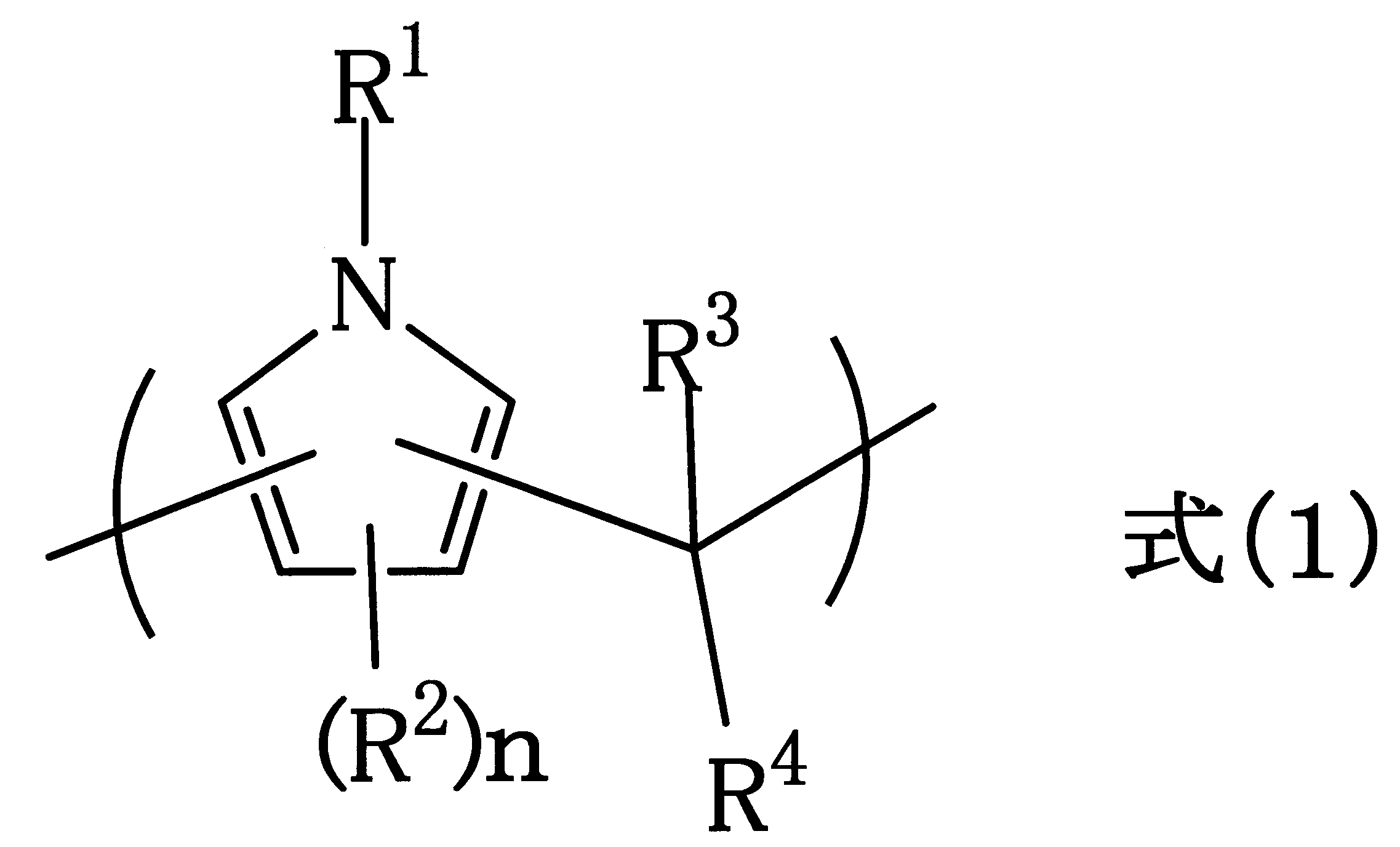
- R 1 is selected from the group consisting of a hydrogen atom, an alkyl group having 1 to 10 carbon atoms, an alkenyl group having 2 to 10 carbon atoms, an aryl group having 6 to 40 carbon atoms, and combinations of these groups.
- the alkyl group, the alkenyl group, or the aryl group may include an ether bond, a ketone bond, or an ester bond
- R 2 represents a halogen group, a nitro group, an amino group, or a hydroxy group.
- R 3 is hydrogen atom, or a halogen group, a nitro group, an amino group, a carbonyl group, An aryl group having 6 to 40 or an aryl group which have good carbon number of 6 to be 40 substituted with a hydroxy group, or a heterocyclic group
- R 4 is a hydrogen atom, or a halogen group, a nitro group, an amino group, Or an alkyl group having 1 to 10 carbon atoms, an aryl group having 6 to 40 carbon atoms, or a heterocyclic group which may be substituted with a hydroxy group, and R 3 and R 4 together with the carbon atom to which they are bonded.
- the alkyl group, the alkenyl group, or the aryl group may contain an ether bond, a ketone bond, or an ester bond
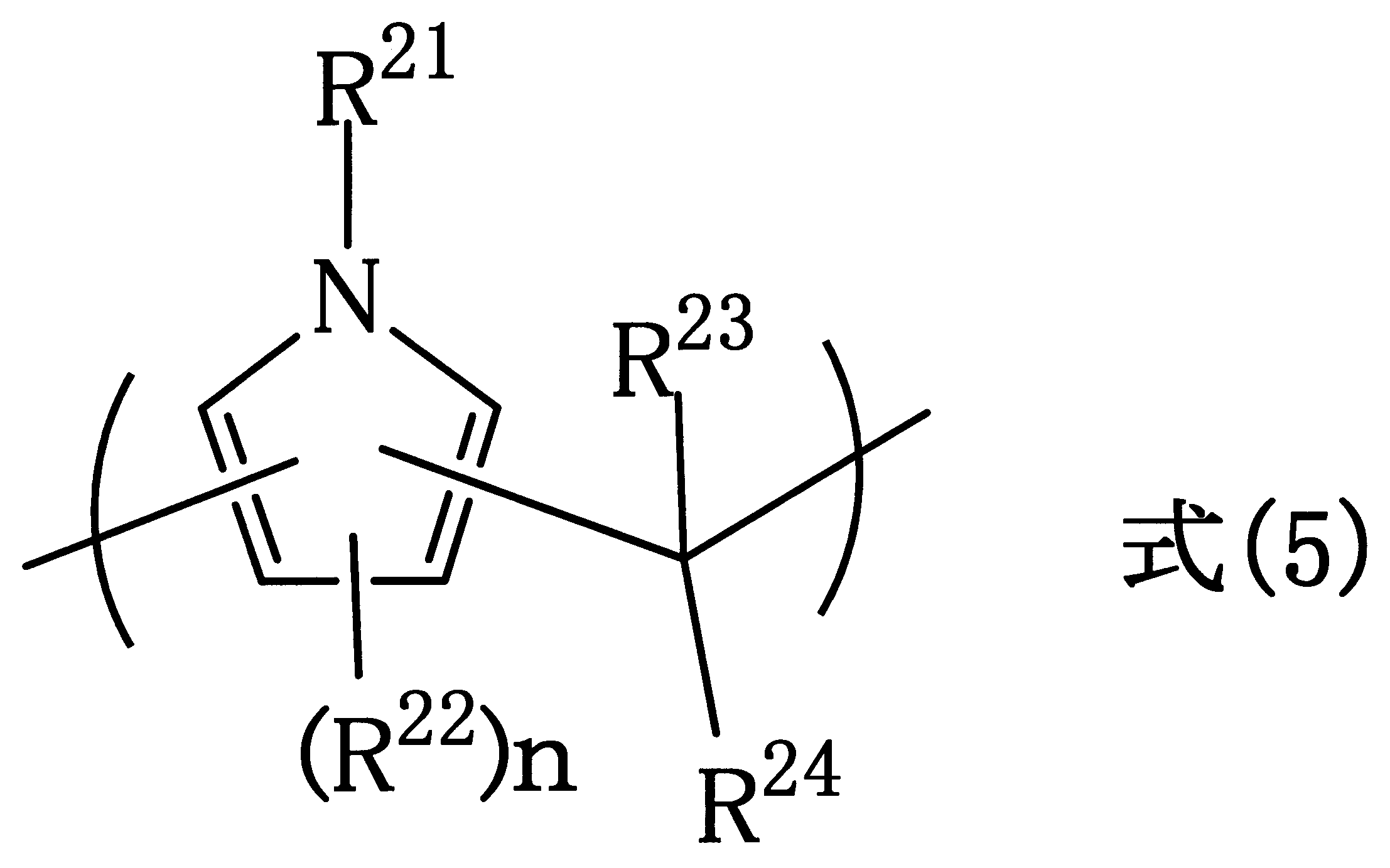
- R 22 represents a halogen group, a nitro group, an amino group, or a hydroxy group. Selected from the group consisting of an alkyl group having 1 to 10 carbon atoms, an alkenyl group having 2 to 10 carbon atoms, an aryl group having 6 to 40 carbon atoms, and a combination of these groups.
- R 23 is hydrogen atom, or a halogen group, a nitro group, an amino group, a carbonyl group An aryl group having 6 to 40 carbon atoms, or an aryl group which have good carbon number of 6 to be 40 substituted with a hydroxy group, or a heterocyclic group
- R 24 is a halogen group, a nitro group, an amino group, or a hydroxy group
- the resist underlayer film forming composition of the present invention With the resist underlayer film forming composition of the present invention, a good resist film pattern shape can be formed without causing intermixing between the upper layer portion of the resist underlayer film and the layer coated thereon.
- the resist underlayer film forming composition of the present invention can be imparted with the ability to efficiently suppress reflection from the substrate, and can also have an effect as an antireflection film for exposure light.
- the resist underlayer film forming composition of the present invention the dry etching rate selectivity close to the resist, the dry etching rate selectivity lower than that of the resist, and the dry etching rate selectivity lower than that of the semiconductor substrate are excellent.
- a resist underlayer film can be provided.
- resist thinning is performed in order to prevent the resist pattern from falling after development.
- the resist pattern is transferred to the lower layer film by an etching process, and the substrate is processed using the lower layer film as a mask, or the resist pattern is transferred to the lower layer film by an etching process.
- a process of repeating the process of transferring the pattern transferred to the lower layer film using a different gas composition and finally processing the substrate is applied.
- the resist underlayer film and the composition for forming the same according to the present invention are effective in these processes.
- a processed substrate for example, a thermal silicon oxide film on the substrate, nitriding
- a silicon film, a polysilicon film, etc. The resist underlayer film of the present invention can be used as a planarizing film, a resist underlayer film, a resist film antifouling film, or a film having dry etch selectivity.
- a resist underlayer film comprising the resist underlayer film forming composition of the present invention is formed on a substrate, a hard mask is formed thereon, a resist film is formed thereon, a resist pattern is formed by exposure and development, and a resist A process may be applied in which a pattern is transferred to a hard mask, a resist pattern transferred to the hard mask is transferred to a resist underlayer film, and a semiconductor substrate is processed with the resist underlayer film. Formation of the hard mask in this process may be performed by a coating-type composition containing an organic polymer or an inorganic polymer and a solvent, or by vacuum deposition of an inorganic substance.
- the deposited material is deposited on the resist underlayer film surface, and at this time, the temperature of the resist underlayer film surface rises to around 400 ° C.
- the polymer to be used is a polymer containing a pyrrole novolac-based unit structure, the heat resistance is extremely high, and thermal degradation does not occur even when the deposited material is deposited.
- This invention is a resist underlayer film forming composition containing the polymer containing the unit structure of Formula (1).
- the polymer containing the unit structure of the formula (1) is a novolak polymer obtained by reacting pyrrole with an aldehyde or a ketone.
- the resist underlayer film forming composition for lithography includes the polymer and a solvent. And it can contain a crosslinking agent and an acid, and can contain additives, such as an acid generator and surfactant, as needed.
- the solid content of the composition is 0.1 to 70% by mass, or 0.1 to 60% by mass. The solid content is the content ratio of all components excluding the solvent from the resist underlayer film forming composition.
- the polymer can be contained in the solid content in a proportion of 1 to 100% by mass, 1 to 99.9% by mass, 50 to 99.9% by mass, 50 to 95% by mass, or 50 to 90% by mass.
- the polymer used in the present invention has a weight average molecular weight of 600 to 1000000 or 600 to 200000.
- R 1 is selected from the group consisting of a hydrogen atom, an alkyl group having 1 to 10 carbon atoms, an alkenyl group having 2 to 10 carbon atoms, an aryl group having 6 to 40 carbon atoms, and combinations of these groups.
- the alkyl group, the alkenyl group, or the aryl group may include an ether bond, a ketone bond, or an ester bond.
- R 2 is composed of a halogen group, a nitro group, an amino group, a hydroxy group, an alkyl group having 1 to 10 carbon atoms, an alkenyl group having 2 to 10 carbon atoms, an aryl group having 6 to 40 carbon atoms, and combinations of these groups.
- the alkyl group, the alkenyl group, or the aryl group may contain an ether bond, a ketone bond, or an ester bond.
- R 3 is a hydrogen atom, a halogen group, a nitro group, an amino group, a carbonyl group, an aryl group having 6 to 40 carbon atoms, an aryl group having 6 to 40 carbon atoms which may be substituted with a hydroxy group, or a heterocyclic ring
- R 4 is a hydrogen atom, an alkyl group having 1 to 10 carbon atoms, an aryl group having 6 to 40 carbon atoms, or a heterocyclic group which may be substituted with a halogen group, a nitro group, an amino group, or a hydroxy group.
- R 3 and R 4 may be combined with the carbon atom to which they are attached to form a ring. These rings may have a structure in which, for example, R 3 and R 4 are each bonded to the 9-position of fluorene. n represents an integer of 0 to 2.
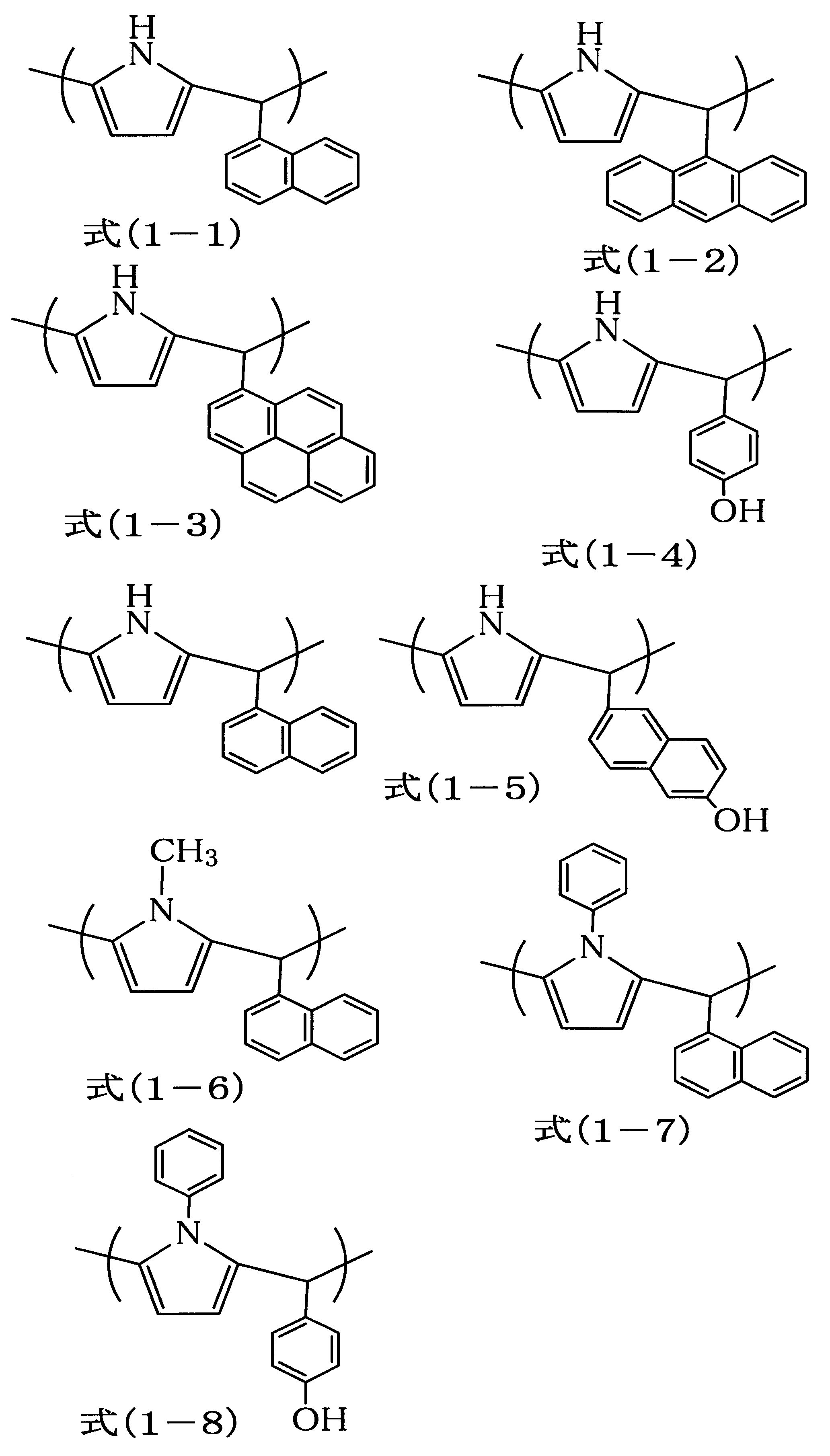
- R 3 in the formula (1) can be a benzene ring, a naphthalene ring, an anthracene ring or a pyrene ring, R 4 can be a hydrogen atom, and n can be 0.
- the halogen group includes a fluorine atom, a chlorine atom, a bromine atom, and an iodine atom.
- aryl group having 6 to 40 carbon atoms for example, when the aryl group having 6 to 40 carbon atoms is a phenyl group and the aryl group having 6 to 40 carbon atoms which may be substituted is a phenyl group, the aryl group is substituted with a phenyl group. And the like phenyl group (namely, biphenyl group).
- alkyl group having 1 to 10 carbon atoms examples include methyl, ethyl, n-propyl, i-propyl, cyclopropyl, n-butyl, i-butyl, s-butyl, t-butyl, cyclobutyl, and 1-methyl-cyclopropyl.
- alkenyl group having 2 to 10 carbon atoms examples include ethenyl, 1-propenyl, 2-propenyl, 1-methyl-1-ethenyl, 1-butenyl, 2-butenyl, 3-butenyl, 2-methyl-1-propenyl, 2 -Methyl-2-propenyl, 1-ethylethenyl, 1-methyl-1-propenyl, 1-methyl-2-propenyl, 1-pentenyl, 2-pentenyl, 3-pentenyl, 4-pentenyl, 1-n-propylethenyl 1-methyl-1-butenyl, 1-methyl-2-butenyl, 1-methyl-3-butenyl, 2-ethyl-2-propenyl, 2-methyl-1-butenyl, 2-methyl-2-butenyl, 2 -Methyl-3-butenyl, 3-methyl-1-butenyl, 3-methyl-2-butenyl, 3-methyl-3-butenyl, 1,1-dimethyl-2-propen
- aryl group having 6 to 40 carbon atoms examples include phenyl group, o-methylphenyl group, m-methylphenyl group, p-methylphenyl group, o-chlorophenyl group, m-chlorophenyl group, p-chlorophenyl group, o-fluorophenyl group, p-fluorophenyl group, o-methoxyphenyl group, p-methoxyphenyl group, p-nitrophenyl group, p-cyanophenyl group, ⁇ -naphthyl group, ⁇ -naphthyl group, o-biphenylyl group M-biphenylyl group, p-biphenylyl group, 1-anthryl group, 2-anthryl group, 9-anthryl group, 1-phenanthryl group, 2-phenanthryl group, 3-phenanthryl group, 4-phenanthryl group and 9-phenanthryl group Ether
- the heterocyclic group is preferably an organic group composed of a 5- to 6-membered heterocyclic ring containing nitrogen, sulfur, and oxygen.
- a pyrrole group, a furan group, a thiophene group, an imidazole group, an oxazole group, a thiazole group, a pyrazole group, An isoxazole group, an isothiazole group, a pyridine group, etc. are mentioned.
- aldehydes used in the production of the polymer of the present invention include formaldehyde, paraformaldehyde, acetaldehyde, propylaldehyde, butyraldehyde, isobutyraldehyde, valeraldehyde, capronaldehyde, 2-methylbutyraldehyde, hexylaldehyde, undecane aldehyde, 7-methoxy- Saturated aliphatic aldehydes such as 3,7-dimethyloctylaldehyde, cyclohexanealdehyde, 3-methyl-2-butyraldehyde, glyoxal, malonaldehyde, succinaldehyde, glutaraldehyde, adipine aldehyde, acrolein, methacrolein, etc.
- an aromatic aldehyde can be preferably used.
- the ketones used in the production of the polymer of the present invention are diaryl ketones, and examples thereof include diphenyl ketone, phenyl naphthyl ketone, dinaphthyl ketone, phenyl tolyl ketone, ditolyl ketone, and 9-fluorenone.
- the polymer used in the present invention is a novolak resin obtained by condensing pyrrole with aldehydes or ketones. In this condensation reaction, aldehydes or ketones can be used at a ratio of 0.1 to 10 equivalents per 1 equivalent of pyrrole.
- Examples of the acid catalyst used in the condensation reaction include mineral acids such as sulfuric acid, phosphoric acid and perchloric acid, organic sulfonic acids such as p-toluenesulfonic acid and p-toluenesulfonic acid monohydrate, formic acid and oxalic acid. These carboxylic acids are used.
- the amount of the acid catalyst used is variously selected depending on the type of acids used. Usually, it is 0.001 to 10000 parts by mass, preferably 0.01 to 1000 parts by mass, and more preferably 0.1 to 100 parts by mass with respect to 100 parts by mass of pyrrole.
- the above condensation reaction is carried out without a solvent, but is usually carried out using a solvent. Any solvent that does not inhibit the reaction can be used. Examples thereof include cyclic ethers such as tetrahydrofuran and dioxane.
- the acid catalyst used is a liquid such as formic acid, it can also serve as a solvent.
- the reaction temperature during the condensation is usually 40 ° C to 200 ° C.
- the reaction time is variously selected depending on the reaction temperature, but is usually about 30 minutes to 50 hours.
- the weight average molecular weight Mw of the polymer obtained as described above is usually 400 to 1000000, 400 to 200000, 400 to 50000, or 600 to 10000.
- the above polymer can be used by mixing other polymers in the whole polymer within 30% by mass.
- these polymers include polyacrylic acid ester compounds, polymethacrylic acid ester compounds, polyacrylamide compounds, polymethacrylamide compounds, polyvinyl compounds, polystyrene compounds, polymaleimide compounds, polymaleic anhydrides, and polyacrylonitrile compounds.
- Examples of the raw material monomer for the polyacrylate compound include methyl acrylate, ethyl acrylate, isopropyl acrylate, benzyl acrylate, naphthyl acrylate, anthryl acrylate, anthryl methyl acrylate, phenyl acrylate, 2-hydroxyethyl acrylate, 2-hydroxypropyl acrylate, 2,2,2-trifluoroethyl acrylate, 4-hydroxybutyl acrylate, isobutyl acrylate, tert-butyl acrylate, cyclohexyl acrylate, isobornyl acrylate, 2-methoxyethyl acrylate, methoxytriethylene glycol acrylate, 2-ethoxyethyl acrylate , Tetrahydrofurfuryl acrylate, 3-methoxybutyl acrylate 2-methyl-2-adamantyl acrylate, 2-ethyl-2-adamantyl acrylate, 2-propyl-2
- Examples of the raw material monomer of the polymethacrylate compound include ethyl methacrylate, normal propyl methacrylate, normal pentyl methacrylate, cyclohexyl methacrylate, benzyl methacrylate, naphthyl methacrylate, anthryl methacrylate, anthryl methyl methacrylate, phenyl methacrylate, 2-phenylethyl methacrylate, 2 -Hydroxyethyl methacrylate, 2-hydroxypropyl methacrylate, 2,2,2-trifluoroethyl methacrylate, 2,2,2-trichloroethyl methacrylate, methyl acrylate (methyl methacrylate?), Isobutyl methacrylate, 2-ethylhexyl methacrylate, isodecyl Methacrylate, normal lauryl methacrylate, Marstearyl methacrylate, methoxydiethylene glycol methacrylate,
- Examples of the raw material monomer for the polyacrylamide compound include acrylamide, N-methylacrylamide, N-ethylacrylamide, N-benzylacrylamide, N-phenylacrylamide, and N, N-dimethylacrylamide.
- Examples of the raw material monomer of the polymethacrylamide compound include methacrylamide, N-methylmethacrylamide, N-ethylmethacrylamide, N-benzylmethacrylamide, N-phenylmethacrylamide, and N, N-dimethylmethacrylamide.
- Examples of the raw material monomer for the polyvinyl compound include vinyl ether, methyl vinyl ether, benzyl vinyl ether, 2-hydroxyethyl vinyl ether, phenyl vinyl ether, and propyl vinyl ether.
- Examples of the raw material monomer for the polystyrene compound include styrene, methylstyrene, chlorostyrene, bromostyrene, and hydroxystyrene.
- Examples of the raw material monomer of the polymaleimide compound include maleimide, N-methylmaleimide, N-phenylmaleimide, and N-cyclohexylmaleimide.
- polymers are produced by dissolving an addition polymerizable monomer and an optionally added chain transfer agent (10% or less based on the mass of the monomer) in an organic solvent, and then adding a polymerization initiator to perform a polymerization reaction. Thereafter, it can be produced by adding a polymerization terminator.
- the addition amount of the polymerization initiator is 1 to 10% with respect to the mass of the monomer, and the addition amount of the polymerization terminator is 0.01 to 0.2% by mass.
- organic solvent used examples include propylene glycol monomethyl ether, propylene glycol monopropyl ether, ethyl lactate, cyclohexanone, methyl ethyl ketone, and dimethylformamide, chain transfer agents such as dodecane thiol and dodecyl thiol, and polymerization initiators such as azo Examples thereof include bisisobutyronitrile and azobiscyclohexanecarbonitrile, and examples of the polymerization terminator include 4-methoxyphenol.
- the reaction temperature is appropriately selected from 30 to 100 ° C.
- the reaction time is appropriately selected from 1 to 48 hours.
- the resist underlayer film forming composition of the present invention can contain a crosslinking agent component.
- the cross-linking agent include melamine-based, substituted urea-based, or polymer systems thereof.
- a cross-linking agent having at least two cross-linking substituents, methoxymethylated glycoluril, butoxymethylated glycoluril, methoxymethylated melamine, butoxymethylated melamine, methoxymethylated benzogwanamine, butoxymethylated benzogwanamine, Compounds such as methoxymethylated urea, butoxymethylated urea, methoxymethylated thiourea, or methoxymethylated thiourea.
- the condensate of these compounds can also be used.
- a crosslinking agent having high heat resistance can be used as the crosslinking agent.
- a crosslinking agent having high heat resistance a compound containing a crosslinking-forming substituent having an aromatic ring (for example, a benzene ring or a naphthalene ring) in the molecule can be preferably used.
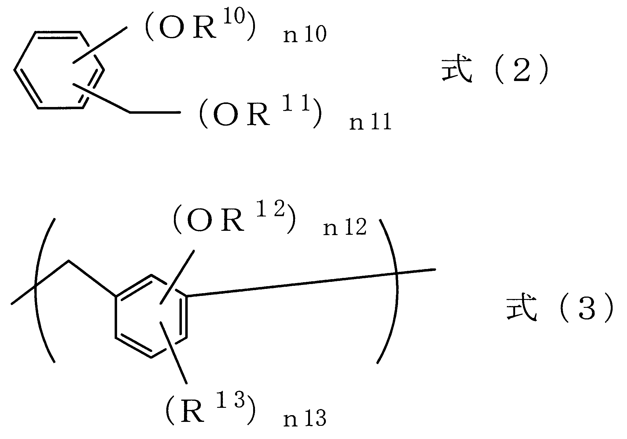
- Examples of this compound include a compound having a partial structure of the following formula (2) and a polymer or oligomer having a repeating unit of the following formula (3).
- R 10 and R 11 are each a hydrogen atom, an alkyl group having 1 to 10 carbon atoms, or an aryl group having 6 to 20 carbon atoms
- n10 is an integer of 1 to 4
- n11 is 1 Is an integer of (5-n10)
- (n10 + n11) is an integer of 2 to 5.
- R 12 is a hydrogen atom or an alkyl group having 1 to 10 carbon atoms
- R 13 is an alkyl group having 1 to 10 carbon atoms
- n12 is an integer of 1 to 4
- n13 is 0 (4-n12), where (n12 + n13) represents an integer of 1 to 4.
- Oligomers and polymers can be used in the range of 2 to 100 or 2 to 50 repeating unit structures.
- alkyl groups and aryl groups can exemplify the above alkyl groups and aryl groups.
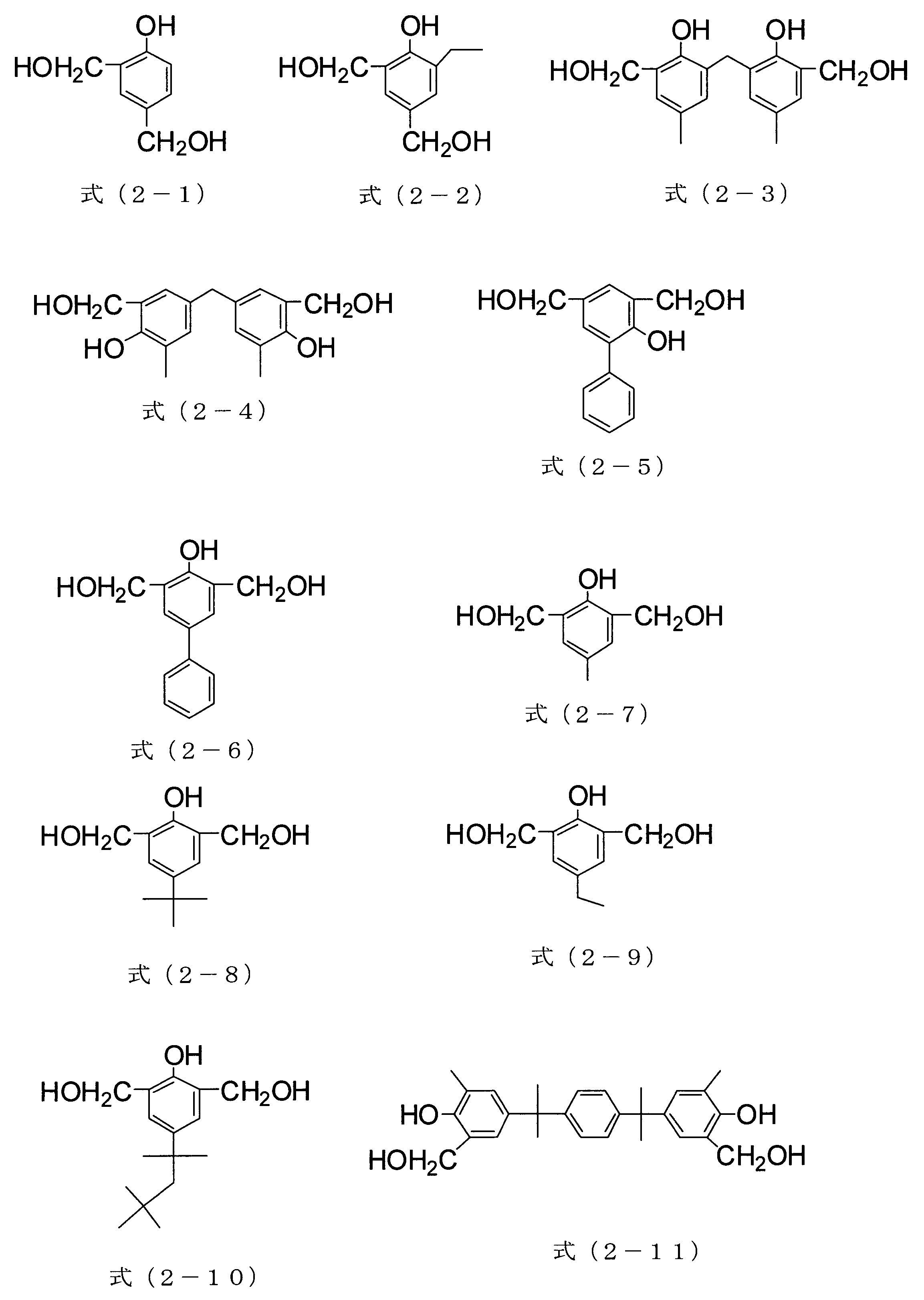
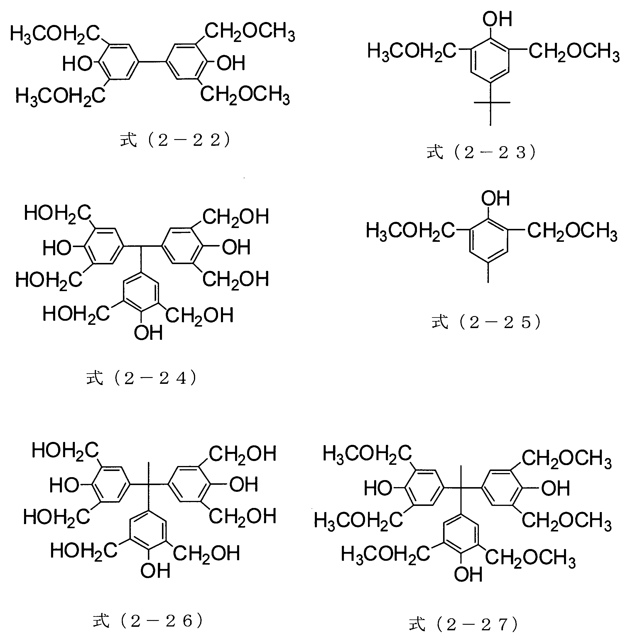
- the above compounds can be obtained as products of Asahi Organic Materials Industry Co., Ltd. and Honshu Chemical Industry Co., Ltd.
- the compound of formula (2-21) can be obtained as Asahi Organic Materials Co., Ltd., trade name TM-BIP-A
- the compound of formula (2-22) is Honshu Chemical Industry Co., Ltd. is available under the trade name TMOM-BP.
- the addition amount of the crosslinking agent varies depending on the coating solvent used, the base substrate used, the required solution viscosity, the required film shape, etc., but is 0.001 to 80% by mass, preferably based on the total solid content. It can be used in an amount of 0.01 to 50% by mass, more preferably 0.05 to 40% by mass.
- These cross-linking agents may cause a cross-linking reaction by self-condensation, but when a cross-linkable substituent is present in the above-mentioned polymer of the present invention, it can cause a cross-linking reaction with those cross-linkable substituents.
- p-toluenesulfonic acid as a catalyst for accelerating the crosslinking reaction, p-toluenesulfonic acid, trifluoromethanesulfonic acid, pyridinium p-toluenesulfonic acid, salicylic acid, sulfosalicylic acid, citric acid, benzoic acid, hydroxybenzoic acid, naphthalenecarbon Acidic compounds such as acids or / and thermal acid generators such as 2,4,4,6-tetrabromocyclohexadienone, benzoin tosylate, 2-nitrobenzyl tosylate, and other organic sulfonic acid alkyl esters may be added.
- the blending amount can be 0.0001 to 20% by mass, preferably 0.0005 to 10% by mass, and more preferably 0.01 to 3% by mass with respect to the total solid content.
- a photoacid generator can be added in order to match the acidity with the photoresist coated on the upper layer in the lithography process.
- Preferred photoacid generators include, for example, onium salt photoacid generators such as bis (4-t-butylphenyl) iodonium trifluoromethanesulfonate, triphenylsulfonium trifluoromethanesulfonate, and phenyl-bis (trichloromethyl) -s.
- -Halogen-containing compound photoacid generators such as triazine, and sulfonic acid photoacid generators such as benzoin tosylate and N-hydroxysuccinimide trifluoromethanesulfonate.
- the photoacid generator is 0.2 to 10% by mass, preferably 0.4 to 5% by mass, based on the total solid content.
- the light absorbing agent examples include commercially available light absorbing agents described in “Technical Dye Technology and Market” (published by CMC) and “Dye Handbook” (edited by the Society of Synthetic Organic Chemistry), such as C.I. I. Disperse Yellow 1,3,4,5,7,8,13,23,31,49,50,51,54,60,64,66,68,79,82,88,90,93,102,114 and 124; C.I. I. D isperse Orange 1, 5, 13, 25, 29, 30, 31, 44, 57, 72 and 73; I. Disperse Red 1, 5, 7, 13, 17, 19, 43, 50, 54, 58, 65, 72, 73, 88, 117, 137, 143, 199 and 210; I.
- Disperse Violet 43; C.I. I. Disperse Blue 96; C.I. I. FluorescentesBrightening Agent 112, 135 and 163; I. Solvent Orange 2 and 45; I. Solvent Red 1, 3, 8, 23, 24, 25, 27 and 49; I. Pigment Green 10; C.I. I. Pigment Brown 2 or the like can be preferably used.
- the above light-absorbing agent is usually blended at a ratio of 10% by mass or less, preferably 5% by mass or less, based on the total solid content of the resist underlayer film material for lithography.
- the rheology modifier mainly improves the fluidity of the resist underlayer film forming composition, and improves the film thickness uniformity of the resist underlayer film and the fillability of the resist underlayer film forming composition inside the hole, particularly in the baking process. It is added for the purpose of enhancing.
- phthalic acid derivatives such as dimethyl phthalate, diethyl phthalate, diisobutyl phthalate, dihexyl phthalate, butyl isodecyl phthalate, adipic acid derivatives such as dinormal butyl adipate, diisobutyl adipate, diisooctyl adipate, octyl decyl adipate
- maleic acid derivatives such as normal butyl maleate, diethyl maleate and dinonyl maleate
- oleic acid derivatives such as methyl oleate, butyl oleate and tetrahydrofurfuryl oleate
- stearic acid derivatives such as normal butyl stearate and glyceryl stearate. it can.
- These rheology modifiers are usually blended at a ratio of less than 30% by mass with respect to the total solid content of the resist underlayer film material for
- the adhesion auxiliary agent is added mainly for the purpose of improving the adhesion between the substrate or resist and the resist underlayer film forming composition, and preventing the resist from being peeled off particularly during development.
- Specific examples include chlorosilanes such as trimethylchlorosilane, dimethylvinylchlorosilane, methyldiphenylchlorosilane, chloromethyldimethylchlorosilane, trimethylmethoxysilane, dimethyldiethoxysilane, methyldimethoxysilane, dimethylvinylethoxysilane, diphenyldimethoxysilane, and phenyltriethoxy.
- Alkoxysilanes such as silane, hexamethyldisilazane, N, N′-bis (trimethylsilyl) urea, silazanes such as dimethyltrimethylsilylamine, trimethylsilylimidazole, vinyltrichlorosilane, ⁇ -chloropropyltrimethoxysilane, ⁇ -aminopropyl Silanes such as triethoxysilane and ⁇ -glycidoxypropyltrimethoxysilane, benzotriazole, benzimidazole , Indazole, imidazole, 2-mercaptobenzimidazole, 2-mercaptobenzothiazole, 2-mercaptobenzoxazole, urazole, thiouracil, mercaptoimidazole, mercaptopyrimidine, etc., 1,1-dimethylurea, 1,3 -Ureas such as dimethylurea or thiourea compounds.
- a surfactant can be blended in order to further improve the applicability to surface unevenness.
- the surfactant include polyoxyethylene lauryl ether, polyoxyethylene stearyl ether, polyoxyethylene cetyl ether, polyoxyethylene alkyl ethers such as polyoxyethylene oleyl ether, polyoxyethylene octylphenol ether, polyoxyethylene nonylphenol ether.
- Polyoxyethylene alkyl allyl ethers Polyoxyethylene alkyl allyl ethers, polyoxyethylene / polyoxypropylene block copolymers, sorbitan monolaurate, sorbitan monopalmitate, sorbitan monostearate, sorbitan monooleate, sorbitan trioleate, sorbitan tristearate, etc.
- Nonionic surfactants such as polyoxyethylene sorbitan fatty acid esters such as tan monopalmitate, polyoxyethylene sorbitan monostearate, polyoxyethylene sorbitan trioleate, polyoxyethylene sorbitan tristearate, F-top EF301, EF303, EF352 (trade name, manufactured by Tochem Products Co., Ltd.), Megafac F171, F173, R-30 (trade name, manufactured by Dainippon Ink Co., Ltd.), Florard FC430, FC431 (trade name, manufactured by Sumitomo 3M Limited) ), Fluorosurfactants such as Asahi Guard AG710, Surflon S-382, SC101, SC102, SC103, SC104, SC105, SC106 (trade name, manufactured by Asahi Glass Co., Ltd.), organosiloxane polymer KP341 (Shin-Ets
- the blending amount of these surfactants is usually 2.0% by mass or less, preferably 1.0% by mass or less, based on the total solid content of the resist underlayer film material for lithography of the present invention.
- These surfactants may be added alone or in combination of two or more.
- the solvent for dissolving the polymer and the crosslinking agent component, the crosslinking catalyst and the like include ethylene glycol monomethyl ether, ethylene glycol monoethyl ether, methyl cellosolve acetate, ethyl cellosolve acetate, diethylene glycol monomethyl ether, diethylene glycol monoethyl ether, Propylene glycol, propylene glycol monomethyl ether, propylene glycol monomethyl ether acetate, propylene glycol monoethyl ether, propylene glycol monoethyl ether acetate, propylene glycol propyl ether acetate, toluene, xylene, methyl ethyl ketone, cyclopentanone, cyclohexanone, 2-hydroxypropionic acid Ethyl, 2-hydroxy- -Ethyl methyl propionate, ethyl ethoxyacetate, ethyl hydroxyacetate, methyl
- a high boiling point solvent such as propylene glycol monobutyl ether and propylene glycol monobutyl ether acetate can be mixed and used.
- a high boiling point solvent such as propylene glycol monobutyl ether and propylene glycol monobutyl ether acetate
- propylene glycol monomethyl ether, propylene glycol monomethyl ether acetate, ethyl lactate, butyl lactate, cyclohexanone and the like are preferable for improving the leveling property.
- the resist used in the present invention is a photoresist or an electron beam resist.
- the photoresist applied on the upper part of the resist underlayer film for lithography in the present invention either negative type or positive type can be used, and a positive type photoresist composed of a novolak resin and 1,2-naphthoquinonediazide sulfonic acid ester, depending on the acid.
- Chemically amplified photoresist comprising a binder having a group that decomposes to increase the alkali dissolution rate and a photoacid generator, a low molecular weight compound and photoacid that increases the alkali dissolution rate of the photoresist by decomposition with an alkali-soluble binder and acid
- Chemically amplified photoresist comprising a generator, comprising a binder having a group that decomposes with acid to increase the alkali dissolution rate, a low-molecular compound that decomposes with acid to increase the alkali dissolution rate of the photoresist, and a photoacid generator Chemically amplified photoresist with Si atoms in the skeleton That there is a photoresist or the like, for example, Rohm & Hearts Co., Ltd., and trade name APEX-E.
- an acid is generated by irradiation with a resin containing an Si-Si bond in the main chain and an aromatic ring at the terminal and an electron beam.
- a composition comprising an acid generator that generates acid, or a poly (p-hydroxystyrene) having a hydroxy group substituted with an organic group containing N-carboxyamine and an acid generator that generates an acid upon irradiation with an electron beam, etc. Is mentioned.
- the acid generated from the acid generator by electron beam irradiation reacts with the N-carboxyaminoxy group of the polymer side chain, and the polymer side chain decomposes into a hydroxy group and exhibits alkali solubility, thus exhibiting alkali development. It dissolves in the liquid to form a resist pattern.
- Acid generators that generate an acid upon irradiation with this electron beam are 1,1-bis [p-chlorophenyl] -2,2,2-trichloroethane, 1,1-bis [p-methoxyphenyl] -2,2,2 -Halogenated organic compounds such as trichloroethane, 1,1-bis [p-chlorophenyl] -2,2-dichloroethane, 2-chloro-6- (trichloromethyl) pyridine, triphenylsulfonium salts, diphenyliodonium salts, etc. Examples thereof include sulfonic acid esters such as onium salts, nitrobenzyl tosylate, and dinitrobenzyl tosylate.
- Alkali amines, tetramethylammonium hydroxide, tetraethylammonium hydroxide, quaternary ammonium salts such as choline, cyclic amines such as pyrrole and piperidine, and alkaline aqueous solutions such as these can be used.
- an appropriate amount of an alcohol such as isopropyl alcohol or a nonionic surfactant may be added to the alkaline aqueous solution.
- preferred developers are quaternary ammonium salts, more preferably tetramethylammonium hydroxide and choline.
- an organic solvent can be used as the developer.
- a spinner, a coater, etc. on a substrate for example, a transparent substrate such as a silicon / silicon dioxide coating, a glass substrate, an ITO substrate
- a substrate for example, a transparent substrate such as a silicon / silicon dioxide coating, a glass substrate, an ITO substrate
- the resist underlayer film forming composition After applying the resist underlayer film forming composition by an appropriate coating method, it is baked and cured to form a coating type underlayer film.
- the thickness of the resist underlayer film is preferably 0.01 to 3.0 ⁇ m.
- the conditions for baking after coating are 80 to 350 ° C. and 0.5 to 120 minutes.
- a good resist pattern can be obtained by performing, developing, rinsing and drying. If necessary, heating after irradiation with light or electron beam (PEB: PostBExposure Bake) can also be performed. Then, the resist underlayer film where the resist has been developed and removed by the above process is removed by dry etching, and a desired pattern can be formed on the substrate.
- PEB PostBExposure Bake
- the exposure light in the photoresist is actinic radiation such as near ultraviolet, far ultraviolet, or extreme ultraviolet (for example, EUV, wavelength 13.5 nm), for example, 248 nm (KrF laser light), 193 nm (ArF laser light), Light having a wavelength such as 157 nm (F 2 laser light) is used.
- the light irradiation can be used without particular limitation as long as it can generate an acid from a photoacid generator, and the exposure dose is 1 to 2000 mJ / cm 2 , 10 to 1500 mJ / cm 2 , or 50 to 50- According to 1000 mJ / cm 2 .
- the electron beam irradiation of an electron beam resist can be performed using, for example, an electron beam irradiation apparatus.
- a step of forming the resist underlayer film on the semiconductor substrate with the resist underlayer film forming composition a step of forming a resist film thereon, a step of forming a resist pattern by light or electron beam irradiation and development, a resist pattern
- a semiconductor device can be manufactured through a step of etching the resist underlayer film and a step of processing the semiconductor substrate with the patterned resist underlayer film.
- the resist underlayer film for lithography which has a selection ratio of dry etching rates close to that of resist, is selected as a resist underlayer film for such processes, and a lower dry etching rate than resist.
- resist underlayer film for lithography having a higher ratio and a resist underlayer film for lithography having a lower dry etching rate selection ratio than a semiconductor substrate.
- a resist underlayer film can be provided with an antireflection ability, and can also have a function of a conventional antireflection film.
- a process of making the resist pattern and the resist underlayer film narrower than the pattern width at the time of developing the resist at the time of the resist underlayer film dry etching has begun to be used.
- a resist underlayer film having a selectivity of a dry etching rate close to that of the resist has been required as a resist underlayer film for such a process.
- such a resist underlayer film can be provided with an antireflection ability, and can also have a function of a conventional antireflection film.
- the substrate after forming the resist underlayer film of the present invention on the substrate, directly or optionally forming one or several layers of coating material on the resist underlayer film on the resist underlayer film.
- a resist can be applied.
- the pattern width of the resist becomes narrow, and even when the resist is thinly coated to prevent pattern collapse, the substrate can be processed by selecting an appropriate etching gas.
- a step of forming the resist underlayer film on the semiconductor substrate with the resist underlayer film forming composition and forming a hard mask by a coating material containing a silicon component or the like or a hard mask (for example, silicon nitride oxide) on the semiconductor substrate.
- a semiconductor device can be manufactured through a step of etching the resist underlayer film with an oxygen-based gas or a hydrogen-based gas and a step of processing a semiconductor substrate with a halogen-based gas with the patterned resist underlayer film.
- the resist underlayer film forming composition for lithography of the present invention has a light absorption site incorporated into the skeleton, so there is no diffused material in the photoresist during heating and drying. Moreover, since the light absorption site has a sufficiently large light absorption performance, the effect of preventing reflected light is high.
- the composition for forming a resist underlayer film for lithography of the present invention has high thermal stability, can prevent contamination of the upper layer film by decomposition products during baking, and can provide a margin for the temperature margin of the baking process. is there. Furthermore, the resist underlayer film material for lithography according to the present invention has a function of preventing reflection of light depending on process conditions, and further prevents the interaction between the substrate and the photoresist or is used for a material or a photoresist used for the photoresist.
- the film can be used as a film having a function of preventing an adverse effect on a substrate of a substance generated during exposure.
- the present invention is a polymer containing the unit structure of the above formula (5).
- the organic group described in the formula (5) can be exemplified by the above formula (1).
- Synthesis example 1 In a 100 ml eggplant flask, 6.0 g of pyrrole (manufactured by Tokyo Chemical Industry Co., Ltd.), 14.1 g of 1-naphthaldehyde (manufactured by Tokyo Chemical Industry Co., Ltd.), p-toluenesulfonic acid monohydrate (Tokyo Chemical Industry Co., Ltd.) )) 1.8 g and toluene (Kanto Chemical Co., Ltd.) 32.8 g was added. Thereafter, the inside of the flask was purged with nitrogen and stirred at room temperature for about 2 hours.
- the reaction mixture was diluted with 15 g of tetrahydrofuran (manufactured by Kanto Chemical Co., Inc.).
- the diluted solution was dropped into 1300 g of methanol (manufactured by Kanto Chemical Co., Ltd.) and reprecipitated.
- the resulting precipitate was suction filtered, and the filtrate was washed with methanol and dried under reduced pressure at 85 ° C. overnight to obtain 16.4 g of a novolak resin.
- the obtained polymer corresponded to Formula (1-1).
- the weight average molecular weight Mw measured in terms of polystyrene by GPC was 7,500.
- Synthesis example 2 In a 200 ml eggplant flask, pyrrole (Tokyo Chemical Industry Co., Ltd.) 6.0 g, 9-anthracene carboxaldehyde (Tokyo Chemical Industry Co., Ltd.) 18.6 g, p-toluenesulfonic acid monohydrate (Tokyo Chemical Industry ( 1.8 g) and 61.6 g of toluene (manufactured by Kanto Chemical Co., Inc.) were added. Thereafter, the inside of the flask was purged with nitrogen, and 6.0 g of pyrrole (manufactured by Tokyo Chemical Industry Co., Ltd.) was added dropwise with stirring at room temperature.
- pyrrole Tokyo Chemical Industry Co., Ltd.
- 9-anthracene carboxaldehyde Tokyo Chemical Industry Co., Ltd.
- p-toluenesulfonic acid monohydrate Tokyo Chemical Industry ( 1.8 g)
- the mixture was stirred at room temperature for about 12 hours.
- the reaction solution was dropped into 1200 g of hexane (manufactured by Kanto Chemical Co., Ltd.) and reprecipitated.
- the obtained precipitate was suction filtered, and the filtrate was washed with hexane and then dried under reduced pressure at 85 ° C. overnight to obtain 20.3 g of a novolak resin.
- the obtained polymer corresponded to Formula (1-2).
- the weight average molecular weight Mw measured in terms of polystyrene by GPC was 2,000.
- Synthesis example 3 In a 100 ml eggplant flask, 2.0 g of pyrrole (manufactured by Tokyo Chemical Industry Co., Ltd.), 7.0 g of 9-pyrenecarboxaldehyde (manufactured by Tokyo Chemical Industry Co., Ltd.), p-toluenesulfonic acid monohydrate (Tokyo Chemical Industry Co., Ltd.) 0.6 g) and 28.6 g of toluene (manufactured by Kanto Chemical Co., Inc.) were added. Thereafter, the inside of the flask was purged with nitrogen, and 2.0 g of pyrrole (manufactured by Tokyo Chemical Industry Co., Ltd.) was added dropwise with stirring at room temperature.
- pyrrole manufactured by Tokyo Chemical Industry Co., Ltd.
- Synthesis example 4 In a 100 ml eggplant flask, pyrrole (Tokyo Chemical Industry Co., Ltd.) 6.0 g, 4-hydroxybenzaldehyde (Tokyo Chemical Industry Co., Ltd.) 10.9 g, methanesulfonic acid (Tokyo Chemical Industry Co., Ltd.) 0.17 g 51.3 g of propylene glycol monomethyl ether was added. Thereafter, the atmosphere in the flask was replaced with nitrogen, and 6.0 g of pyrrole (manufactured by Tokyo Chemical Industry Co., Ltd.) was added dropwise with stirring at room temperature. After completion of the dropwise addition, the mixture was heated and stirred at reflux for about 15 hours.
- the methanesulfonic acid was removed by contacting with an ion exchange resin to obtain 66.7 g of a novolak resin solution having a solid content of 17.6%.
- the obtained polymer corresponded to the formula (1-4).
- the weight average molecular weight Mw measured by GPC by polystyrene conversion was 660.
- Synthesis example 5 In a 200 ml eggplant flask, 7.0 g of pyrrole (manufactured by Tokyo Chemical Industry Co., Ltd.), 13.4 g of 1-naphthaldehyde (manufactured by Tokyo Chemical Industry Co., Ltd.), 6-hydroxy-2-naphthaldehyde (Tokyo Chemical Industry Co., Ltd.) 3.7 g), 0.41 g of methanesulfonic acid (manufactured by Tokyo Chemical Industry Co., Ltd.), and 57.3 g of propylene glycol monomethyl ether.
- the reaction solution was dropped into 1500 g of methanol (manufactured by Kanto Chemical Co., Inc.) and reprecipitated.
- the obtained precipitate was filtered by suction, and the filtrate was washed with methanol and dried under reduced pressure at 85 ° C. overnight to obtain 12.1 g of a novolak resin.
- the obtained polymer corresponded to the formula (1-6).
- the weight average molecular weight Mw measured in terms of polystyrene by GPC was 2,200.
- Synthesis example 7 In a 100 ml eggplant flask, 6.0 g of 1-phenylpyrrole (manufactured by Tokyo Chemical Industry Co., Ltd.), 6.5 g of 1-naphthaldehyde (manufactured by Tokyo Chemical Industry Co., Ltd.), and 37.7 g of propylene glycol monomethyl ether acetate were placed. Thereafter, the atmosphere in the flask was replaced with nitrogen, and 0.04 g of methanesulfonic acid (manufactured by Tokyo Chemical Industry Co., Ltd.) was added dropwise with stirring at room temperature. After completion of dropping, the mixture was heated to 110 ° C. and stirred for about 17 hours.
- the reaction solution was dropped into 1000 g of methanol (manufactured by Kanto Chemical Co., Inc.) and reprecipitated.
- the obtained precipitate was suction filtered, and the filtrate was washed with methanol and dried under reduced pressure at 85 ° C. overnight to obtain 9.5 g of a novolak resin.
- the obtained polymer corresponded to the formula (1-7).
- the weight average molecular weight Mw measured in terms of polystyrene by GPC was 2,500.
- Synthesis example 8 In a 100 ml eggplant flask, 7.0 g of 1-phenylpyrrole (manufactured by Tokyo Chemical Industry Co., Ltd.), 6.0 g of 4-hydroxybenzaldehyde (manufactured by Tokyo Chemical Industry Co., Ltd.), and 30.4 g of propylene glycol monomethyl ether acetate were placed. Thereafter, the atmosphere in the flask was replaced with nitrogen, and 0.05 g of methanesulfonic acid (manufactured by Tokyo Chemical Industry Co., Ltd.) was added dropwise with stirring at room temperature. After completion of dropping, the mixture was heated to 110 ° C. and stirred for about 17 hours.
- the methanesulfonic acid was removed by contacting with an ion exchange resin to obtain 42.4 g of a novolak resin solution having a solid content of 24.5 percent.
- the obtained polymer corresponded to the formula (1-8).
- the weight average molecular weight Mw measured in terms of polystyrene by GPC was 2,300.
- Example 1 To 0.8 g of the polymer obtained in Synthesis Example 1, 1.0 g of propylene glycol monomethyl ether acetate, 2.5 g of propylene glycol monomethyl ether, 6.4 g of cyclohexanone, TMOM-BP (the above formula (2-22), 0.16 g of Honshu Chemical Industry Co., Ltd. and 0.016 g of TAG2689 were added and dissolved to prepare a resist underlayer film forming composition solution for use in a lithography process using a multilayer film.
- TMOM-BP the above formula (2-22
- TAG2689 0.016 g of TAG2689
- Example 2 To 2.0 g of the polymer obtained in Synthesis Example 2, 9.7 g of propylene glycol monomethyl ether acetate, 6.5 g of propylene glycol monomethyl ether, 16.2 g of cyclohexanone, 0.4 g of tetramethoxymethyl glycoluril, 0.4 g of pyridinium paratoluenesulfonate. 04 g was added and dissolved to prepare a resist underlayer film forming composition solution for use in a lithography process using a multilayer film.
- Example 3 To 0.8 g of the polymer obtained in Synthesis Example 3, 1.0 g of propylene glycol monomethyl ether acetate, 2.5 g of propylene glycol monomethyl ether, 6.4 g of cyclohexanone, TMOM-BP (formula (2-22), 0.16 g of Honshu Chemical Industry Co., Ltd. and 0.016 g of TAG2689 were added and dissolved to prepare a resist underlayer film forming composition solution for use in a lithography process using a multilayer film.
- Example 4 To 12.0 g of the polymer solution obtained in Synthesis Example 4, 4.6 g of propylene glycol monomethyl ether acetate, 6.3 g of propylene glycol monomethyl ether, 2.3 g of cyclohexanone, and TMOM-BP (the above formula (2-22) as a crosslinking agent) , Manufactured by Honshu Chemical Industry Co., Ltd.) and 0.03 g of pyridinium p-toluenesulfonate were added and dissolved to prepare a resist underlayer film forming composition solution for use in a lithography process using a multilayer film.
- TMOM-BP the above formula (2-22) as a crosslinking agent
- Example 5 To 2.0 g of the polymer obtained in Synthesis Example 5, 11.0 g of propylene glycol monomethyl ether acetate, 6.6 g of propylene glycol monomethyl ether, 4.4 g of cyclohexanone, and TMOM-BP (formula (2-22), 0.4 g of Honshu Chemical Industry Co., Ltd. and 0.03 g of pyridinium p-toluenesulfonate were added and dissolved to prepare a resist underlayer film forming composition solution for use in a lithography process using a multilayer film.
- TMOM-BP formula (2-22
- Example 6 To 1.5 g of the polymer obtained in Synthesis Example 6, 11.5 g of propylene glycol monomethyl ether acetate, 3.3 g of propylene glycol monomethyl ether, 1.6 g of cyclohexanone, and TMOM-BP (formula (2-22), Honshu Chemical Industry Co., Ltd.) (0.3 g) and pyridinium p-toluenesulfonate (0.02 g) were added and dissolved to prepare a resist underlayer film forming composition solution for use in a lithography process using a multilayer film.
- TMOM-BP formula (2-22), Honshu Chemical Industry Co., Ltd.
- Example 7 To 1.5 g of the polymer obtained in Synthesis Example 7, 11.5 g of propylene glycol monomethyl ether acetate, 3.3 g of propylene glycol monomethyl ether, 1.6 g of cyclohexanone, and TMOM-BP (formula (2-22), Honshu Chemical Industry Co., Ltd.) (0.3 g) and pyridinium p-toluenesulfonate (0.02 g) were added and dissolved to prepare a resist underlayer film forming composition solution for use in a lithography process using a multilayer film.
- TMOM-BP formula (2-22), Honshu Chemical Industry Co., Ltd.
- Example 8 To 12.0 g of the polymer solution obtained in Synthesis Example 8, 6.4 g of propylene glycol monomethyl ether acetate, 13.5 g of propylene glycol monomethyl ether, 3.2 g of cyclohexanone, and TMOM-BP (formula (2-22) above) as a crosslinking agent , Honshu Chemical Industry Co., Ltd.) was added and dissolved in 0.04 g of pyridinium p-toluenesulfonate to prepare a resist underlayer film forming composition solution for use in a lithography process using a multilayer film.
- TMOM-BP formula (2-22) above
- Example 9 To the 12.0 g polymer solution obtained in Synthesis Example 4, propylene glycol monomethyl ether acetate 4.6 g, propylene glycol monomethyl ether 6.3 g, cyclohexanone 2.3 g, tetramethoxymethyl glycoluril 0.4 g, pyridinium paratoluenesulfonate 0 0.03 g was added and dissolved to prepare a resist underlayer film forming composition solution for use in a lithography process using a multilayer film.
- Comparative Example 1 1.0 g of the polymer compound (formula (4-1)) obtained in Comparative Synthesis Example 1 was added to 0.2 g of tetramethoxymethyl glycoluril, 0.02 g of pyridinium paratoluenesulfonate, Megafac R-30 (Dainippon) Ink Chemical Co., Ltd., trade name) 0.003 g, propylene glycol monomethyl ether 2.3 g, propylene glycol monomethyl ether acetate 4.6 g, and cyclohexanone 16.3 g were mixed to obtain a solution.
- the solution is filtered using a polyethylene microfilter having a pore size of 0.10 ⁇ m, further filtered using a polyethylene microfilter having a pore size of 0.05 ⁇ m, and a solution of a resist underlayer film forming composition used in a lithography process using a multilayer film Was prepared.
- the pattern is a pattern in which the distance from the hole center to the adjacent hole center is one time the diameter of the hole.
- Each resist underlayer film forming composition solution prepared in Examples 1 to 9 and Comparative Example 1 was applied onto a silicon wafer by a spinner. Heating was performed on a hot plate at a temperature of 240 ° C. for 1 minute to form a resist underlayer film (film thickness 0.2 ⁇ m). The dry etching rate was measured for the resist underlayer film using CF 4 gas as an etching gas. Further, a solution obtained by dissolving 0.7 g of phenol novolak resin in 10 g of propylene glycol monomethyl ether was applied onto a silicon wafer by a spinner and heated at a temperature of 240 ° C. for 1 minute to form a phenol novolak resin film.
- the dry etching rate was measured for the resin film using CF 4 gas as an etching gas, and each resist underlayer film formed from the resist underlayer film forming compositions of Examples 1 to 9 and Comparative Example 1 was dried. Comparison was made with the etching rate. The results are shown in Table 3 below.
- the dry etching rate ratio in Table 3 is the dry etching rate of each resist underlayer film (the above resist underlayer film) / (phenol novolac resin film) relative to the dry etching rate of the phenol novolak resin film.
- the resist underlayer film obtained from the resist underlayer film forming composition according to the present invention is different from the conventional high etch rate antireflection film, and is selected with a dry etching rate close to or smaller than that of the photoresist. It can be seen that it is possible to provide an excellent coating-type resist underlayer film that has a low dry etching rate selection ratio as compared with a semiconductor substrate and can also have an effect as an antireflection film.
Abstract
Description
第2観点として、式(1)のR3がベンゼン環、ナフタレン環、アントラセン環又はピレン環であり、R4が水素原子であり、nが0である第1観点に記載のレジスト下層膜形成組成物、
第3観点として、更に架橋剤を含む第1観点又は第2観点に記載のレジスト下層膜形成組成物、
第4観点として、更に酸及び/又は酸発生剤を含む第1観点乃至第3観点のいずれか一つに記載のレジスト下層膜形成組成物、
第5観点として、第1観点乃至第4観点のいずれか一つに記載のレジスト下層膜形成組成物を半導体基板上に塗布し焼成することによって得られるレジスト下層膜、
第6観点として、第1観点乃至第4観点のいずれか一つに記載のレジスト下層膜形成組成物を半導体基板上に塗布し焼成して下層膜を形成する工程を含む半導体の製造に用いるレジストパターンの形成方法、
第7観点として、半導体基板上に第1観点乃至第4観点のいずれか一つに記載のレジスト下層膜形成組成物により下層膜を形成する工程、その上にレジスト膜を形成する工程、光又は電子線の照射と現像によりレジストパターンを形成する工程、レジストパターンにより該下層膜をエッチングする工程、及びパターン化された下層膜により半導体基板を加工する工程を含む半導体装置の製造方法、
第8観点として、半導体基板に第1観点乃至第4観点のいずれか一つに記載のレジスト下層膜形成組成物により下層膜を形成する工程、その上にハードマスクを形成する工程、更にその上にレジスト膜を形成する工程、光又は電子線の照射と現像によりレジストパターンを形成する工程、レジストパターンによりハードマスクをエッチングする工程、パターン化されたハードマスクにより該下層膜をエッチングする工程、及びパターン化された下層膜により半導体基板を加工する工程を含む半導体装置の製造方法、
第9観点として、ハードマスクが無機物の蒸着によるものである第8観点に記載の製造方法、及び
第10観点として、下記式(5):
As a second aspect, the resist underlayer film formation according to the first aspect, wherein R 3 in the formula (1) is a benzene ring, naphthalene ring, anthracene ring or pyrene ring, R 4 is a hydrogen atom, and n is 0 Composition,
As a third aspect, the resist underlayer film forming composition according to the first aspect or the second aspect further containing a crosslinking agent,
As a fourth aspect, the resist underlayer film forming composition according to any one of the first aspect to the third aspect, further comprising an acid and / or an acid generator,
As a fifth aspect, a resist underlayer film obtained by applying and baking the resist underlayer film forming composition according to any one of the first to fourth aspects on a semiconductor substrate,
As a sixth aspect, a resist used for manufacturing a semiconductor including a step of applying a resist underlayer film forming composition according to any one of the first to fourth aspects onto a semiconductor substrate and baking to form an underlayer film Pattern formation method,
As a seventh aspect, a step of forming an underlayer film with the resist underlayer film forming composition according to any one of the first to fourth aspects on a semiconductor substrate, a step of forming a resist film thereon, light or A method of manufacturing a semiconductor device, comprising: a step of forming a resist pattern by electron beam irradiation and development; a step of etching the lower layer film with a resist pattern; and a step of processing a semiconductor substrate with a patterned lower layer film;
As an eighth aspect, a step of forming an underlayer film on the semiconductor substrate with the resist underlayer film forming composition according to any one of the first to fourth aspects, a step of forming a hard mask thereon, and further thereon A step of forming a resist film on the substrate, a step of forming a resist pattern by light and electron beam irradiation and development, a step of etching a hard mask with the resist pattern, a step of etching the lower layer film with a patterned hard mask, and A method of manufacturing a semiconductor device including a step of processing a semiconductor substrate with a patterned underlayer film,
As a ninth aspect, the manufacturing method according to the eighth aspect, in which the hard mask is formed by vapor deposition of an inorganic substance, and as the tenth aspect, the following formula (5):
本発明のレジスト下層膜形成組成物には、基板からの反射を効率的に抑制する性能を付与することも可能であり、露光光の反射防止膜としての効果を併せ持つこともできる。
本発明のレジスト下層膜形成組成物により、レジストに近いドライエッチング速度の選択比、レジストに比べて小さいドライエッチング速度の選択比や半導体基板に比べて小さいドライエッチング速度の選択比を持つ、優れたレジスト下層膜を提供することができる。 With the resist underlayer film forming composition of the present invention, a good resist film pattern shape can be formed without causing intermixing between the upper layer portion of the resist underlayer film and the layer coated thereon.
The resist underlayer film forming composition of the present invention can be imparted with the ability to efficiently suppress reflection from the substrate, and can also have an effect as an antireflection film for exposure light.
With the resist underlayer film forming composition of the present invention, the dry etching rate selectivity close to the resist, the dry etching rate selectivity lower than that of the resist, and the dry etching rate selectivity lower than that of the semiconductor substrate are excellent. A resist underlayer film can be provided.
そして、本発明のレジスト下層膜は、平坦化膜、レジスト下層膜、レジスト膜層の汚染防止膜、ドライエッチ選択性を有する膜として用いることができる。これにより、半導体製造のリソグラフィープロセスにおけるレジストパターン形成を、容易に、精度良く行うことができる。 With the miniaturization of resist patterns, resist thinning is performed in order to prevent the resist pattern from falling after development. In such a thin film resist, the resist pattern is transferred to the lower layer film by an etching process, and the substrate is processed using the lower layer film as a mask, or the resist pattern is transferred to the lower layer film by an etching process. A process of repeating the process of transferring the pattern transferred to the lower layer film using a different gas composition and finally processing the substrate is applied. The resist underlayer film and the composition for forming the same according to the present invention are effective in these processes. When a substrate is processed using the resist underlayer film of the present invention, a processed substrate (for example, a thermal silicon oxide film on the substrate, nitriding) A silicon film, a polysilicon film, etc.).
The resist underlayer film of the present invention can be used as a planarizing film, a resist underlayer film, a resist film antifouling film, or a film having dry etch selectivity. Thereby, resist pattern formation in the lithography process of semiconductor manufacture can be performed easily and accurately.
本発明において上記のリソグラフィー用レジスト下層膜形成組成物は、上記ポリマーと溶剤を含む。そして、架橋剤と酸を含むことができ、必要に応じて酸発生剤、界面活性剤等の添加剤を含むことができる。この組成物の固形分は0.1~70質量%、又は0.1~60質量%である。固形分は、レジスト下層膜形成組成物から溶剤を除いた全成分の含有割合である。固形分中に上記ポリマーを1~100質量%、1~99.9質量%、50~99.9質量%、50~95質量%、又は50~90質量%の割合で含有することができる。
本発明に用いるポリマーは、重量平均分子量が600~1000000、又は600~200000である。 This invention is a resist underlayer film forming composition containing the polymer containing the unit structure of Formula (1). The polymer containing the unit structure of the formula (1) is a novolak polymer obtained by reacting pyrrole with an aldehyde or a ketone.
In the present invention, the resist underlayer film forming composition for lithography includes the polymer and a solvent. And it can contain a crosslinking agent and an acid, and can contain additives, such as an acid generator and surfactant, as needed. The solid content of the composition is 0.1 to 70% by mass, or 0.1 to 60% by mass. The solid content is the content ratio of all components excluding the solvent from the resist underlayer film forming composition. The polymer can be contained in the solid content in a proportion of 1 to 100% by mass, 1 to 99.9% by mass, 50 to 99.9% by mass, 50 to 95% by mass, or 50 to 90% by mass.
The polymer used in the present invention has a weight average molecular weight of 600 to 1000000 or 600 to 200000.
縮合時の反応温度は、通常40℃~200℃である。反応時間は、反応温度によって種々選択されるが、通常30分~50時間程度である。
以上のようにして得られる重合体の重量平均分子量Mwは、通常400~1000000、400~200000、400~50000、又は600~10000である。 The above condensation reaction is carried out without a solvent, but is usually carried out using a solvent. Any solvent that does not inhibit the reaction can be used. Examples thereof include cyclic ethers such as tetrahydrofuran and dioxane. In addition, if the acid catalyst used is a liquid such as formic acid, it can also serve as a solvent.
The reaction temperature during the condensation is usually 40 ° C to 200 ° C. The reaction time is variously selected depending on the reaction temperature, but is usually about 30 minutes to 50 hours.
The weight average molecular weight Mw of the polymer obtained as described above is usually 400 to 1000000, 400 to 200000, 400 to 50000, or 600 to 10000.
それらポリマーとしては、ポリアクリル酸エステル化合物、ポリメタクリル酸エステル化合物、ポリアクリルアミド化合物、ポリメタクリルアミド化合物、ポリビニル化合物、ポリスチレン化合物、ポリマレイミド化合物、ポリマレイン酸無水物、及びポリアクリロニトリル化合物が挙げられる。 The above polymer can be used by mixing other polymers in the whole polymer within 30% by mass.
Examples of these polymers include polyacrylic acid ester compounds, polymethacrylic acid ester compounds, polyacrylamide compounds, polymethacrylamide compounds, polyvinyl compounds, polystyrene compounds, polymaleimide compounds, polymaleic anhydrides, and polyacrylonitrile compounds.
式(2)中、R10及びR11はそれぞれ水素原子、炭素数1~10のアルキル基、又は炭素数6~20のアリール基であり、n10は1~4の整数であり、n11は1~(5-n10)の整数であり、(n10+n11)は2~5の整数を示す。
式(3)中、R12は水素原子又は炭素数1~10のアルキル基であり、R13は炭素数1~10のアルキル基であり、n12は1~4の整数であり、n13は0~(4-n12)であり、(n12+n13)は1~4の整数を示す。オリゴマー及びポリマーは繰り返し単位構造の数が2~100、又は2~50の範囲で用いることができる。 Examples of this compound include a compound having a partial structure of the following formula (2) and a polymer or oligomer having a repeating unit of the following formula (3).
In the formula (2), R 10 and R 11 are each a hydrogen atom, an alkyl group having 1 to 10 carbon atoms, or an aryl group having 6 to 20 carbon atoms, n10 is an integer of 1 to 4, and n11 is 1 Is an integer of (5-n10), and (n10 + n11) is an integer of 2 to 5.
In the formula (3), R 12 is a hydrogen atom or an alkyl group having 1 to 10 carbon atoms, R 13 is an alkyl group having 1 to 10 carbon atoms, n12 is an integer of 1 to 4, and n13 is 0 (4-n12), where (n12 + n13) represents an integer of 1 to 4. Oligomers and polymers can be used in the range of 2 to 100 or 2 to 50 repeating unit structures.

本発明におけるリソグラフィー用レジスト下層膜の上部に塗布されるフォトレジストとしてはネガ型、ポジ型いずれも使用でき、ノボラック樹脂と1,2-ナフトキノンジアジドスルホン酸エステルとからなるポジ型フォトレジスト、酸により分解してアルカリ溶解速度を上昇させる基を有するバインダーと光酸発生剤からなる化学増幅型フォトレジスト、アルカリ可溶性バインダーと酸により分解してフォトレジストのアルカリ溶解速度を上昇させる低分子化合物と光酸発生剤からなる化学増幅型フォトレジスト、酸により分解してアルカリ溶解速度を上昇させる基を有するバインダーと酸により分解してフォトレジストのアルカリ溶解速度を上昇させる低分子化合物と光酸発生剤からなる化学増幅型フォトレジスト、骨格にSi原子を有するフォトレジスト等があり、例えば、ロームアンドハーツ社製、商品名APEX-Eが挙げられる。 The resist used in the present invention is a photoresist or an electron beam resist.
As the photoresist applied on the upper part of the resist underlayer film for lithography in the present invention, either negative type or positive type can be used, and a positive type photoresist composed of a novolak resin and 1,2-naphthoquinonediazide sulfonic acid ester, depending on the acid. Chemically amplified photoresist comprising a binder having a group that decomposes to increase the alkali dissolution rate and a photoacid generator, a low molecular weight compound and photoacid that increases the alkali dissolution rate of the photoresist by decomposition with an alkali-soluble binder and acid Chemically amplified photoresist comprising a generator, comprising a binder having a group that decomposes with acid to increase the alkali dissolution rate, a low-molecular compound that decomposes with acid to increase the alkali dissolution rate of the photoresist, and a photoacid generator Chemically amplified photoresist with Si atoms in the skeleton That there is a photoresist or the like, for example, Rohm & Hearts Co., Ltd., and trade name APEX-E.
更に、本発明のリソグラフィー用レジスト下層膜材料は、プロセス条件によっては、光の反射を防止する機能と、更には基板とフォトレジストとの相互作用の防止或いはフォトレジストに用いられる材料又はフォトレジストへの露光時に生成する物質の基板への悪作用を防ぐ機能とを有する膜としての使用が可能である。 The composition for forming a resist underlayer film for lithography of the present invention has high thermal stability, can prevent contamination of the upper layer film by decomposition products during baking, and can provide a margin for the temperature margin of the baking process. is there.
Furthermore, the resist underlayer film material for lithography according to the present invention has a function of preventing reflection of light depending on process conditions, and further prevents the interaction between the substrate and the photoresist or is used for a material or a photoresist used for the photoresist. The film can be used as a film having a function of preventing an adverse effect on a substrate of a substance generated during exposure.
100mlナスフラスコにピロール(東京化成工業(株)製)6.0g、1-ナフトアルデヒド(東京化成工業(株)製)14.1g、p-トルエンスルホン酸一水和物(東京化成工業(株)製)1.8g、トルエン(関東化学(株)製)32.8gを入れた。その後フラスコ内を窒素置換した後、室温で約2時間撹拌した。反応終了後、テトラヒドロフラン(関東化学(株)製)15gで希釈した。希釈液をメタノール(関東化学(株)製)1300gに滴下し、再沈殿させた。得られた沈殿物を吸引ろ過し、ろ物をメタノールで洗浄後、85℃で一晩減圧乾燥しノボラック樹脂を16.4g得た。得られたポリマーは式(1-1)に相当した。GPCによりポリスチレン換算で測定される重量平均分子量Mwは、7,500であった。 Synthesis example 1
In a 100 ml eggplant flask, 6.0 g of pyrrole (manufactured by Tokyo Chemical Industry Co., Ltd.), 14.1 g of 1-naphthaldehyde (manufactured by Tokyo Chemical Industry Co., Ltd.), p-toluenesulfonic acid monohydrate (Tokyo Chemical Industry Co., Ltd.) )) 1.8 g and toluene (Kanto Chemical Co., Ltd.) 32.8 g was added. Thereafter, the inside of the flask was purged with nitrogen and stirred at room temperature for about 2 hours. After completion of the reaction, the reaction mixture was diluted with 15 g of tetrahydrofuran (manufactured by Kanto Chemical Co., Inc.). The diluted solution was dropped into 1300 g of methanol (manufactured by Kanto Chemical Co., Ltd.) and reprecipitated. The resulting precipitate was suction filtered, and the filtrate was washed with methanol and dried under reduced pressure at 85 ° C. overnight to obtain 16.4 g of a novolak resin. The obtained polymer corresponded to Formula (1-1). The weight average molecular weight Mw measured in terms of polystyrene by GPC was 7,500.
200mlナスフラスコにピロール(東京化成工業(株)製)6.0g、9-アントラセンカルボキシアルデヒド(東京化成工業(株)製)18.6g、p-トルエンスルホン酸一水和物(東京化成工業(株)製)1.8g、トルエン(関東化学(株)製)61.6gを入れた。その後、フラスコ内を窒素置換した後、室温で撹拌しながらピロール(東京化成工業(株)製)6.0gを滴下した。滴下終了後、室温で約12時間撹拌した。反応終了後、反応溶液をヘキサン(関東化学(株)製)1200gに滴下し、再沈殿させた。得られた沈殿物を吸引ろ過し、ろ物をヘキサンで洗浄後、85℃で一晩減圧乾燥しノボラック樹脂を20.3g得た。得られたポリマーは式(1-2)に相当した。GPCによりポリスチレン換算で測定される重量平均分子量Mwは、2,000であった。 Synthesis example 2
In a 200 ml eggplant flask, pyrrole (Tokyo Chemical Industry Co., Ltd.) 6.0 g, 9-anthracene carboxaldehyde (Tokyo Chemical Industry Co., Ltd.) 18.6 g, p-toluenesulfonic acid monohydrate (Tokyo Chemical Industry ( 1.8 g) and 61.6 g of toluene (manufactured by Kanto Chemical Co., Inc.) were added. Thereafter, the inside of the flask was purged with nitrogen, and 6.0 g of pyrrole (manufactured by Tokyo Chemical Industry Co., Ltd.) was added dropwise with stirring at room temperature. After completion of dropping, the mixture was stirred at room temperature for about 12 hours. After completion of the reaction, the reaction solution was dropped into 1200 g of hexane (manufactured by Kanto Chemical Co., Ltd.) and reprecipitated. The obtained precipitate was suction filtered, and the filtrate was washed with hexane and then dried under reduced pressure at 85 ° C. overnight to obtain 20.3 g of a novolak resin. The obtained polymer corresponded to Formula (1-2). The weight average molecular weight Mw measured in terms of polystyrene by GPC was 2,000.
100mlナスフラスコにピロール(東京化成工業(株)製)2.0g、9-ピレンカルボキシアルデヒド(東京化成工業(株)製)7.0g、p-トルエンスルホン酸一水和物(東京化成工業(株)製)0.6g、トルエン(関東化学(株)製)28.6gを入れた。その後フラスコ内を窒素置換した後、室温で撹拌しながらピロール(東京化成工業(株)製)2.0gを滴下した。滴下終了後、室温で約1時間撹拌し、更に加熱して約22時間還流撹拌した。反応終了後、テトラヒドロフラン(関東化学(株)製)15gを加えて析出した固体を溶解させた。溶液をヘキサン(関東化学(株)製)1200gに滴下し、再沈殿させた。得られた沈殿物を吸引ろ過し、ろ物をヘキサンで洗浄後、85℃で一晩減圧乾燥しノボラック樹脂を6.9g得た。得られたポリマーは式(1-3)に相当した。GPCによりポリスチレン換算で測定される重量平均分子量Mwは、900であった。 Synthesis example 3
In a 100 ml eggplant flask, 2.0 g of pyrrole (manufactured by Tokyo Chemical Industry Co., Ltd.), 7.0 g of 9-pyrenecarboxaldehyde (manufactured by Tokyo Chemical Industry Co., Ltd.), p-toluenesulfonic acid monohydrate (Tokyo Chemical Industry Co., Ltd.) 0.6 g) and 28.6 g of toluene (manufactured by Kanto Chemical Co., Inc.) were added. Thereafter, the inside of the flask was purged with nitrogen, and 2.0 g of pyrrole (manufactured by Tokyo Chemical Industry Co., Ltd.) was added dropwise with stirring at room temperature. After completion of dropping, the mixture was stirred at room temperature for about 1 hour, further heated, and stirred at reflux for about 22 hours. After completion of the reaction, 15 g of tetrahydrofuran (manufactured by Kanto Chemical Co., Inc.) was added to dissolve the precipitated solid. The solution was dropped into 1200 g of hexane (manufactured by Kanto Chemical Co., Ltd.) and reprecipitated. The resulting precipitate was filtered with suction, and the filtrate was washed with hexane and then dried under reduced pressure at 85 ° C. overnight to obtain 6.9 g of novolak resin. The obtained polymer corresponded to Formula (1-3). The weight average molecular weight Mw measured in terms of polystyrene by GPC was 900.
100mlナスフラスコにピロール(東京化成工業(株)製)6.0g、4-ヒドロキシベンズアルデヒド(東京化成工業(株)製)10.9g、メタンスルホン酸(東京化成工業(株)製)0.17g、プロピレングリコールモノメチルエーテル51.3gを入れた。その後フラスコ内を窒素置換した後、室温で撹拌しながらピロール(東京化成工業(株)製)6.0gを滴下した。滴下終了後、加熱して約15時間還流撹拌した。反応終了後、イオン交換樹脂と接触させてメタンスルホン酸を除去し、固形分17.6%のノボラック樹脂溶液を66.7g得た。得られたポリマーは式(1-4)に相当した。GPCによりポリスチレン換算で測定される重量平均分子量Mwは、660であった。 Synthesis example 4
In a 100 ml eggplant flask, pyrrole (Tokyo Chemical Industry Co., Ltd.) 6.0 g, 4-hydroxybenzaldehyde (Tokyo Chemical Industry Co., Ltd.) 10.9 g, methanesulfonic acid (Tokyo Chemical Industry Co., Ltd.) 0.17 g 51.3 g of propylene glycol monomethyl ether was added. Thereafter, the atmosphere in the flask was replaced with nitrogen, and 6.0 g of pyrrole (manufactured by Tokyo Chemical Industry Co., Ltd.) was added dropwise with stirring at room temperature. After completion of the dropwise addition, the mixture was heated and stirred at reflux for about 15 hours. After completion of the reaction, the methanesulfonic acid was removed by contacting with an ion exchange resin to obtain 66.7 g of a novolak resin solution having a solid content of 17.6%. The obtained polymer corresponded to the formula (1-4). The weight average molecular weight Mw measured by GPC by polystyrene conversion was 660.
200mlナスフラスコにピロール(東京化成工業(株)製)7.0g、1-ナフトアルデヒド(東京化成工業(株)製)13.4g、6-ヒドロキシ-2-ナフトアルデヒド(東京化成工業(株)製)3.7g、メタンスルホン酸(東京化成工業(株)製)0.41g、プロピレングリコールモノメチルエーテル57.3gを入れた。その後フラスコ内を窒素置換した後、室温で撹拌しながらピロール(東京化成工業(株)製)7.0gを滴下した。滴下終了後、室温で約14時間撹拌した。反応終了後、反応溶液をメタノール(関東化学(株)製)1600gに滴下し、再沈殿させた。得られた沈殿物を吸引ろ過し、ろ物をメタノールで洗浄後、85℃で一晩減圧乾燥しノボラック樹脂を11.9g得た。得られたポリマーは式(1-5)に相当した。GPCによりポリスチレン換算で測定される重量平均分子量Mwは、2,300であった。 Synthesis example 5
In a 200 ml eggplant flask, 7.0 g of pyrrole (manufactured by Tokyo Chemical Industry Co., Ltd.), 13.4 g of 1-naphthaldehyde (manufactured by Tokyo Chemical Industry Co., Ltd.), 6-hydroxy-2-naphthaldehyde (Tokyo Chemical Industry Co., Ltd.) 3.7 g), 0.41 g of methanesulfonic acid (manufactured by Tokyo Chemical Industry Co., Ltd.), and 57.3 g of propylene glycol monomethyl ether. Thereafter, the inside of the flask was purged with nitrogen, and 7.0 g of pyrrole (manufactured by Tokyo Chemical Industry Co., Ltd.) was added dropwise with stirring at room temperature. After completion of dropping, the mixture was stirred at room temperature for about 14 hours. After completion of the reaction, the reaction solution was dropped into 1600 g of methanol (manufactured by Kanto Chemical Co., Inc.) and reprecipitated. The obtained precipitate was filtered by suction, and the filtrate was washed with methanol and dried under reduced pressure at 85 ° C. overnight to obtain 11.9 g of a novolak resin. The obtained polymer corresponded to the formula (1-5). The weight average molecular weight Mw measured in terms of polystyrene by GPC was 2,300.
100mlナスフラスコに1-メチルピロール(東京化成工業(株)製)6.0g、1-ナフトアルデヒド(東京化成工業(株)製)11.6g、メタンスルホン酸(東京化成工業(株)製)0.07g、プロピレングリコールモノメチルエーテルアセテート52.9gを入れた。その後フラスコ内を窒素置換した後、室温で撹拌しながら1-メチルピロール(東京化成工業(株)製)6.0gを滴下した。滴下終了後、室温で四日間撹拌した。反応終了後、反応溶液をメタノール(関東化学(株)製)1500gに滴下し、再沈殿させた。得られた沈殿物を吸引ろ過し、ろ物をメタノールで洗浄後、85℃で一晩減圧乾燥しノボラック樹脂を12.1g得た。得られたポリマーは式(1-6)に相当した。GPCによりポリスチレン換算で測定される重量平均分子量Mwは、2,200であった。 Synthesis Example 6
In a 100 ml eggplant flask, 6.0 g of 1-methylpyrrole (Tokyo Chemical Industry Co., Ltd.), 11.6 g of 1-naphthaldehyde (Tokyo Chemical Industry Co., Ltd.), methanesulfonic acid (Tokyo Chemical Industry Co., Ltd.) 0.07 g and 52.9 g of propylene glycol monomethyl ether acetate were added. Thereafter, the flask was purged with nitrogen, and 6.0 g of 1-methylpyrrole (manufactured by Tokyo Chemical Industry Co., Ltd.) was added dropwise with stirring at room temperature. After completion of dropping, the mixture was stirred at room temperature for 4 days. After completion of the reaction, the reaction solution was dropped into 1500 g of methanol (manufactured by Kanto Chemical Co., Inc.) and reprecipitated. The obtained precipitate was filtered by suction, and the filtrate was washed with methanol and dried under reduced pressure at 85 ° C. overnight to obtain 12.1 g of a novolak resin. The obtained polymer corresponded to the formula (1-6). The weight average molecular weight Mw measured in terms of polystyrene by GPC was 2,200.
100mlナスフラスコに1-フェニルピロール(東京化成工業(株)製)6.0g、1-ナフトアルデヒド(東京化成工業(株)製)6.5g、プロピレングリコールモノメチルエーテルアセテート37.7gを入れた。その後フラスコ内を窒素置換した後、室温で撹拌しながらメタンスルホン酸(東京化成工業(株)製)0.04gを滴下した。滴下終了後、110℃に加熱して約17時間撹拌した。反応終了後、反応溶液をメタノール(関東化学(株)製)1000gに滴下し、再沈殿させた。得られた沈殿物を吸引ろ過し、ろ物をメタノールで洗浄後、85℃で一晩減圧乾燥しノボラック樹脂を9.5g得た。得られたポリマーは式(1-7)に相当した。GPCによりポリスチレン換算で測定される重量平均分子量Mwは、2,500であった。 Synthesis example 7
In a 100 ml eggplant flask, 6.0 g of 1-phenylpyrrole (manufactured by Tokyo Chemical Industry Co., Ltd.), 6.5 g of 1-naphthaldehyde (manufactured by Tokyo Chemical Industry Co., Ltd.), and 37.7 g of propylene glycol monomethyl ether acetate were placed. Thereafter, the atmosphere in the flask was replaced with nitrogen, and 0.04 g of methanesulfonic acid (manufactured by Tokyo Chemical Industry Co., Ltd.) was added dropwise with stirring at room temperature. After completion of dropping, the mixture was heated to 110 ° C. and stirred for about 17 hours. After completion of the reaction, the reaction solution was dropped into 1000 g of methanol (manufactured by Kanto Chemical Co., Inc.) and reprecipitated. The obtained precipitate was suction filtered, and the filtrate was washed with methanol and dried under reduced pressure at 85 ° C. overnight to obtain 9.5 g of a novolak resin. The obtained polymer corresponded to the formula (1-7). The weight average molecular weight Mw measured in terms of polystyrene by GPC was 2,500.
100mlナスフラスコに1-フェニルピロール(東京化成工業(株)製)7.0g、4-ヒドロキシベンズアルデヒド(東京化成工業(株)製)6.0g、プロピレングリコールモノメチルエーテルアセテート30.4gを入れた。その後フラスコ内を窒素置換した後、室温で撹拌しながらメタンスルホン酸(東京化成工業(株)製)0.05g、を滴下した。滴下終了後、110℃に加熱して約17時間撹拌した。反応終了後、イオン交換樹脂と接触させてメタンスルホン酸を除去し、固形分24.5パーセントのノボラック樹脂溶液を42.4g得た。得られたポリマーは式(1-8)に相当した。GPCによりポリスチレン換算で測定される重量平均分子量Mwは、2,300であった。 Synthesis example 8
In a 100 ml eggplant flask, 7.0 g of 1-phenylpyrrole (manufactured by Tokyo Chemical Industry Co., Ltd.), 6.0 g of 4-hydroxybenzaldehyde (manufactured by Tokyo Chemical Industry Co., Ltd.), and 30.4 g of propylene glycol monomethyl ether acetate were placed. Thereafter, the atmosphere in the flask was replaced with nitrogen, and 0.05 g of methanesulfonic acid (manufactured by Tokyo Chemical Industry Co., Ltd.) was added dropwise with stirring at room temperature. After completion of dropping, the mixture was heated to 110 ° C. and stirred for about 17 hours. After completion of the reaction, the methanesulfonic acid was removed by contacting with an ion exchange resin to obtain 42.4 g of a novolak resin solution having a solid content of 24.5 percent. The obtained polymer corresponded to the formula (1-8). The weight average molecular weight Mw measured in terms of polystyrene by GPC was 2,300.
窒素下、100ml四口フラスコにカルバゾール(10g、0.060mol、東京化成工業(株)製)、ベンズアルデヒド(6.41g、0.060mol、純正化学(株)製)、p-トルエンスルホン酸一水和物(1.19g、0.060mol、関東化学(株)製)を加え、1,4-ジオキサン(15g、関東化学(株)製)を加え撹拌し、100℃まで昇温し溶解させ重合を開始した。2時間後60℃まで放冷後、クロロホルム(50g、関東化学(株)製)を加え希釈し、メタノール(250g、関東化学(株)製)へ再沈殿させた。得られた沈殿物をろ過し、減圧乾燥機で60℃、10時間、更に120℃、24時間乾燥し、目的とする高分子化合物8.64gを得た。これは下記式(4-1)の単位構造を含むポリマーであった。高分子化合物(式(4-1))のGPCによるポリスチレン換算で測定される重量平均分子量Mwは4000、多分散度Mw/Mnは1.69であった。

Under nitrogen, carbazole (10 g, 0.060 mol, manufactured by Tokyo Chemical Industry Co., Ltd.), benzaldehyde (6.41 g, 0.060 mol, manufactured by Junsei Chemical Co., Ltd.), p-toluenesulfonic acid monohydrate in a 100 ml four-necked flask A Japanese product (1.19 g, 0.060 mol, manufactured by Kanto Chemical Co., Inc.) was added, 1,4-dioxane (15 g, manufactured by Kanto Chemical Co., Ltd.) was added, and the mixture was stirred and heated to 100 ° C. to dissolve and polymerize. Started. Two hours later, the mixture was allowed to cool to 60 ° C., diluted with chloroform (50 g, manufactured by Kanto Chemical Co., Inc.), and reprecipitated into methanol (250 g, manufactured by Kanto Chemical Co., Inc.). The obtained precipitate was filtered and dried with a vacuum dryer at 60 ° C. for 10 hours, further at 120 ° C. for 24 hours to obtain 8.64 g of the intended polymer compound. This was a polymer containing a unit structure of the following formula (4-1). The weight average molecular weight Mw of the polymer compound (formula (4-1)) measured by polystyrene conversion by GPC was 4000, and the polydispersity Mw / Mn was 1.69.
合成例1で得た0.8gのポリマーに、プロピレングリコールモノメチルエーテルアセテート1.0g、プロピレングリコールモノメチルエーテル2.5g、シクロヘキサノン6.4g、架橋剤としてTMOM-BP(上記式(2-22)、本州化学工業(株)製)を0.16g、TAG2689を0.016g加えて溶解させ、多層膜によるリソグラフィープロセスに用いるレジスト下層膜形成組成物の溶液を調製した。 Example 1
To 0.8 g of the polymer obtained in Synthesis Example 1, 1.0 g of propylene glycol monomethyl ether acetate, 2.5 g of propylene glycol monomethyl ether, 6.4 g of cyclohexanone, TMOM-BP (the above formula (2-22), 0.16 g of Honshu Chemical Industry Co., Ltd. and 0.016 g of TAG2689 were added and dissolved to prepare a resist underlayer film forming composition solution for use in a lithography process using a multilayer film.
合成例2で得た2.0gのポリマーに、プロピレングリコールモノメチルエーテルアセテート9.7g、プロピレングリコールモノメチルエーテル6.5g、シクロヘキサノン16.2g、テトラメトキシメチルグリコールウリル0.4g、ピリジニウムパラトルエンスルホネート0.04g加えて溶解させ、多層膜によるリソグラフィープロセスに用いるレジスト下層膜形成組成物の溶液を調製した。 Example 2
To 2.0 g of the polymer obtained in Synthesis Example 2, 9.7 g of propylene glycol monomethyl ether acetate, 6.5 g of propylene glycol monomethyl ether, 16.2 g of cyclohexanone, 0.4 g of tetramethoxymethyl glycoluril, 0.4 g of pyridinium paratoluenesulfonate. 04 g was added and dissolved to prepare a resist underlayer film forming composition solution for use in a lithography process using a multilayer film.
合成例3で得た0.8gのポリマーに、プロピレングリコールモノメチルエーテルアセテート1.0g、プロピレングリコールモノメチルエーテル2.5g、シクロヘキサノン6.4g、架橋剤としてTMOM-BP(上記式(2-22)、本州化学工業(株)製)を0.16g、TAG2689を0.016g加えて溶解させ、多層膜によるリソグラフィープロセスに用いるレジスト下層膜形成組成物の溶液を調製した。 Example 3
To 0.8 g of the polymer obtained in Synthesis Example 3, 1.0 g of propylene glycol monomethyl ether acetate, 2.5 g of propylene glycol monomethyl ether, 6.4 g of cyclohexanone, TMOM-BP (formula (2-22), 0.16 g of Honshu Chemical Industry Co., Ltd. and 0.016 g of TAG2689 were added and dissolved to prepare a resist underlayer film forming composition solution for use in a lithography process using a multilayer film.
合成例4で得た12.0gのポリマー溶液に、プロピレングリコールモノメチルエーテルアセテート4.6g、プロピレングリコールモノメチルエーテル6.3g、シクロヘキサノン2.3g、架橋剤としてTMOM-BP(上記式(2-22)、本州化学工業(株)製)を0.4g、ピリジニウムパラトルエンスルホネート0.03g加えて溶解させ、多層膜によるリソグラフィープロセスに用いるレジスト下層膜形成組成物の溶液を調製した。 Example 4
To 12.0 g of the polymer solution obtained in Synthesis Example 4, 4.6 g of propylene glycol monomethyl ether acetate, 6.3 g of propylene glycol monomethyl ether, 2.3 g of cyclohexanone, and TMOM-BP (the above formula (2-22) as a crosslinking agent) , Manufactured by Honshu Chemical Industry Co., Ltd.) and 0.03 g of pyridinium p-toluenesulfonate were added and dissolved to prepare a resist underlayer film forming composition solution for use in a lithography process using a multilayer film.
合成例5で得た2.0gのポリマーに、プロピレングリコールモノメチルエーテルアセテート11.0g、プロピレングリコールモノメチルエーテル6.6g、シクロヘキサノン4.4g、架橋剤としてTMOM-BP(上記式(2-22)、本州化学工業(株)製)を0.4g、ピリジニウムパラトルエンスルホネート0.03g加えて溶解させ、多層膜によるリソグラフィープロセスに用いるレジスト下層膜形成組成物の溶液を調製した。 Example 5
To 2.0 g of the polymer obtained in Synthesis Example 5, 11.0 g of propylene glycol monomethyl ether acetate, 6.6 g of propylene glycol monomethyl ether, 4.4 g of cyclohexanone, and TMOM-BP (formula (2-22), 0.4 g of Honshu Chemical Industry Co., Ltd. and 0.03 g of pyridinium p-toluenesulfonate were added and dissolved to prepare a resist underlayer film forming composition solution for use in a lithography process using a multilayer film.
合成例6で得た1.5gのポリマーに、プロピレングリコールモノメチルエーテルアセテート11.5g、プロピレングリコールモノメチルエーテル3.3g、シクロヘキサノン1.6g、架橋剤としてTMOM-BP(上記式(2-22)、本州化学工業(株)製)を0.3g、ピリジニウムパラトルエンスルホネート0.02g加えて溶解させ、多層膜によるリソグラフィープロセスに用いるレジスト下層膜形成組成物の溶液を調製した。 Example 6
To 1.5 g of the polymer obtained in Synthesis Example 6, 11.5 g of propylene glycol monomethyl ether acetate, 3.3 g of propylene glycol monomethyl ether, 1.6 g of cyclohexanone, and TMOM-BP (formula (2-22), Honshu Chemical Industry Co., Ltd.) (0.3 g) and pyridinium p-toluenesulfonate (0.02 g) were added and dissolved to prepare a resist underlayer film forming composition solution for use in a lithography process using a multilayer film.
合成例7で得た1.5gのポリマーに、プロピレングリコールモノメチルエーテルアセテート11.5g、プロピレングリコールモノメチルエーテル3.3g、シクロヘキサノン1.6g、架橋剤としてTMOM-BP(上記式(2-22)、本州化学工業(株)製)を0.3g、ピリジニウムパラトルエンスルホネート0.02g加えて溶解させ、多層膜によるリソグラフィープロセスに用いるレジスト下層膜形成組成物の溶液を調製した。 Example 7
To 1.5 g of the polymer obtained in Synthesis Example 7, 11.5 g of propylene glycol monomethyl ether acetate, 3.3 g of propylene glycol monomethyl ether, 1.6 g of cyclohexanone, and TMOM-BP (formula (2-22), Honshu Chemical Industry Co., Ltd.) (0.3 g) and pyridinium p-toluenesulfonate (0.02 g) were added and dissolved to prepare a resist underlayer film forming composition solution for use in a lithography process using a multilayer film.
合成例8で得た12.0gのポリマー溶液に、プロピレングリコールモノメチルエーテルアセテート6.4g、プロピレングリコールモノメチルエーテル13.5g、シクロヘキサノン3.2g、架橋剤としてTMOM-BP(上記式(2-22)、本州化学工業(株)製)を0.6g、ピリジニウムパラトルエンスルホネート0.04g加えて溶解させ、多層膜によるリソグラフィープロセスに用いるレジスト下層膜形成組成物の溶液を調製した。 Example 8
To 12.0 g of the polymer solution obtained in Synthesis Example 8, 6.4 g of propylene glycol monomethyl ether acetate, 13.5 g of propylene glycol monomethyl ether, 3.2 g of cyclohexanone, and TMOM-BP (formula (2-22) above) as a crosslinking agent , Honshu Chemical Industry Co., Ltd.) was added and dissolved in 0.04 g of pyridinium p-toluenesulfonate to prepare a resist underlayer film forming composition solution for use in a lithography process using a multilayer film.
合成例4で得た12.0gのポリマー溶液に、プロピレングリコールモノメチルエーテルアセテート4.6g、プロピレングリコールモノメチルエーテル6.3g、シクロヘキサノン2.3g、テトラメトキシメチルグリコールウリル0.4g、ピリジニウムパラトルエンスルホネート0.03g加えて溶解させ、多層膜によるリソグラフィープロセスに用いるレジスト下層膜形成組成物の溶液を調製した。 Example 9
To the 12.0 g polymer solution obtained in Synthesis Example 4, propylene glycol monomethyl ether acetate 4.6 g, propylene glycol monomethyl ether 6.3 g, cyclohexanone 2.3 g, tetramethoxymethyl glycoluril 0.4 g, pyridinium paratoluenesulfonate 0 0.03 g was added and dissolved to prepare a resist underlayer film forming composition solution for use in a lithography process using a multilayer film.
上記比較合成例1で得た高分子化合物(式(4-1))の1.0gに、テトラメトキシメチルグリコールウリル0.2g、ピリジニウムパラトルエンスルホネート0.02g、メガファックR-30(大日本インキ化学(株)製、商品名)0.003g、プロピレングリコールモノメチルエーテル2.3g、プロピレングリコールモノメチルエーテルアセテート4.6g、シクロヘキサノン16.3gを混合して溶液とした。その後、孔径0.10μmのポリエチレン製ミクロフィルターを用いてろ過し、更に、孔径0.05μmのポリエチレン製ミクロフィルターを用いてろ過して、多層膜によるリソグラフィープロセスに用いるレジスト下層膜形成組成物の溶液を調製した。 Comparative Example 1
1.0 g of the polymer compound (formula (4-1)) obtained in Comparative Synthesis Example 1 was added to 0.2 g of tetramethoxymethyl glycoluril, 0.02 g of pyridinium paratoluenesulfonate, Megafac R-30 (Dainippon) Ink Chemical Co., Ltd., trade name) 0.003 g, propylene glycol monomethyl ether 2.3 g, propylene glycol monomethyl ether acetate 4.6 g, and cyclohexanone 16.3 g were mixed to obtain a solution. Thereafter, the solution is filtered using a polyethylene microfilter having a pore size of 0.10 μm, further filtered using a polyethylene microfilter having a pore size of 0.05 μm, and a solution of a resist underlayer film forming composition used in a lithography process using a multilayer film Was prepared.
実施例1~9、及び比較例1で調製した各レジスト下層膜形成組成物溶液を、スピンコーターを用いてシリコンウェハー上にそれぞれ塗布した。ホットプレート上で250℃1分間焼成し、レジスト下層膜(膜厚0.05μm)を形成した。そして、これらのレジスト下層膜を、分光エリプソメーターを用いて波長193nmでの屈折率(n値)及び光学吸光係数(k値、減衰係数とも呼ぶ)を測定した。結果を表1に示した。
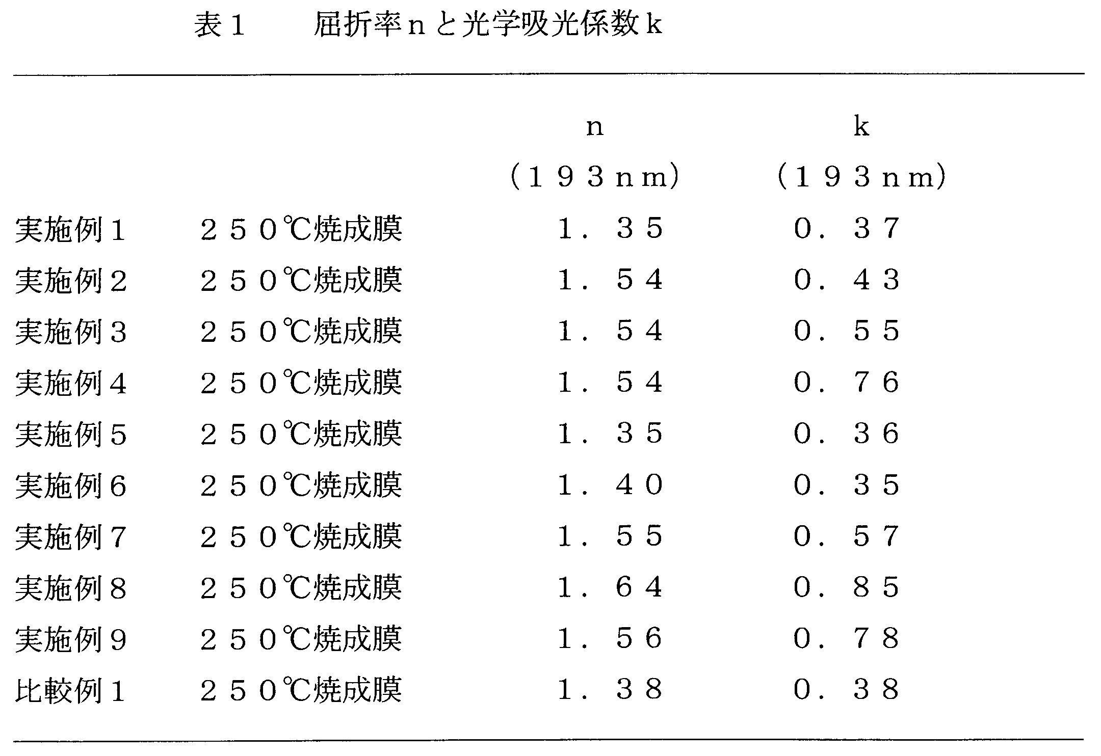
Each resist underlayer film forming composition solution prepared in Examples 1 to 9 and Comparative Example 1 was applied onto a silicon wafer using a spin coater. Baking was performed at 250 ° C. for 1 minute on a hot plate to form a resist underlayer film (film thickness 0.05 μm). Then, the refractive index (n value) and the optical extinction coefficient (also referred to as k value or attenuation coefficient) at a wavelength of 193 nm were measured for these resist underlayer films using a spectroscopic ellipsometer. The results are shown in Table 1.
実施例1~9、及び比較例1で調製した各レジスト下層膜形成組成物溶液を、スピナーによりシリコンウェハー上に塗布した。ホットプレート上で250℃の温度で1分間加熱し、レジスト下層膜(膜厚0.2μm)を形成した。そして、これらのレジスト下層膜を、フォトレジストに使用する溶剤である、乳酸エチル、プロピレングリコールモノメチルエーテル及びプロピレングリコールモノメチルエーテルアセテートに浸漬し、その溶剤に不溶であることを確認した。 (Elution test for photoresist solvent)
Each resist underlayer film forming composition solution prepared in Examples 1 to 9 and Comparative Example 1 was applied onto a silicon wafer by a spinner. A resist underlayer film (film thickness 0.2 μm) was formed by heating on a hot plate at a temperature of 250 ° C. for 1 minute. Then, these resist underlayer films were immersed in ethyl lactate, propylene glycol monomethyl ether and propylene glycol monomethyl ether acetate, which are solvents used for the photoresist, and confirmed to be insoluble in the solvent.
実施例1~9、及び比較例1で得た本発明のリソグラフィー用下層膜形成組成物溶液を、スピンコーターにより、ホール(直径0.13μm、深さ0.7μm)を有するSiO2付きウェハー基板上に塗布した。パターンは、ホール中心から隣のホール中心までの間隔が、当該ホールの直径の1倍であるパターンである。 (Embeddability test)
The wafer substrate with SiO 2 having holes (diameter 0.13 μm, depth 0.7 μm) obtained from the lower layer film forming composition solution for lithography of the present invention obtained in Examples 1 to 9 and Comparative Example 1 using a spin coater It was applied on top. The pattern is a pattern in which the distance from the hole center to the adjacent hole center is one time the diameter of the hole.

ドライエッチング速度の測定には、下記のエッチング装置及びエッチングガスを用いた。
エッチング装置:RIE-10NR(サムコ(株)製)
エッチングガス:CF4 (Measurement of dry etching rate)
The following etching apparatus and etching gas were used for the measurement of the dry etching rate.
Etching device: RIE-10NR (manufactured by Samco)
Etching gas: CF 4
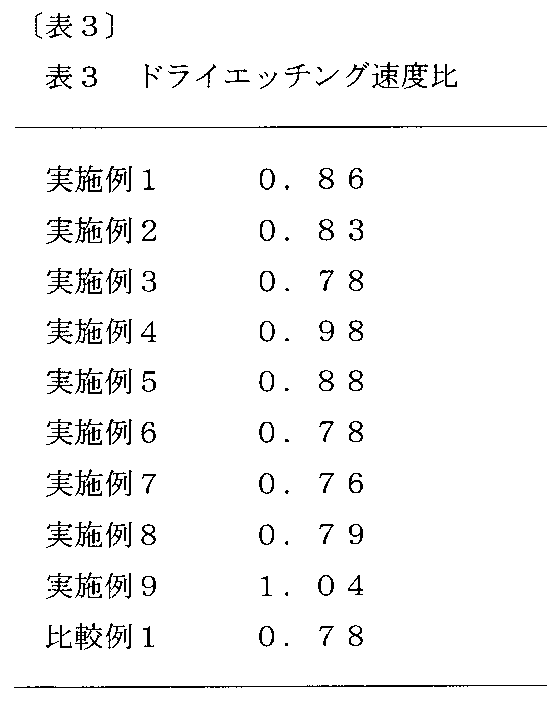
Claims (10)
- 下記式(1):

- 式(1)のR3がベンゼン環、ナフタレン環、アントラセン環又はピレン環であり、R4が水素原子であり、nが0である請求項1に記載のレジスト下層膜形成組成物。 The resist underlayer film forming composition according to claim 1, wherein R 3 in the formula (1) is a benzene ring, a naphthalene ring, an anthracene ring or a pyrene ring, R 4 is a hydrogen atom, and n is 0.
- 更に架橋剤を含む請求項1又は請求項2に記載のレジスト下層膜形成組成物。 Furthermore, the resist underlayer film forming composition of Claim 1 or Claim 2 containing a crosslinking agent.
- 更に酸及び/又は酸発生剤を含む請求項1乃至請求項3のいずれか1項に記載のレジスト下層膜形成組成物。 The resist underlayer film forming composition according to any one of claims 1 to 3, further comprising an acid and / or an acid generator.
- 請求項1乃至請求項4のいずれか1項に記載のレジスト下層膜形成組成物を半導体基板上に塗布し焼成することによって得られるレジスト下層膜。 A resist underlayer film obtained by applying and baking the resist underlayer film forming composition according to any one of claims 1 to 4 on a semiconductor substrate.
- 請求項1乃至請求項4のいずれか1項に記載のレジスト下層膜形成組成物を半導体基板上に塗布し焼成して下層膜を形成する工程を含む半導体の製造に用いるレジストパターンの形成方法。 A method for forming a resist pattern, which is used for manufacturing a semiconductor, comprising a step of applying the resist underlayer film forming composition according to any one of claims 1 to 4 on a semiconductor substrate and baking the composition to form an underlayer film.
- 半導体基板上に請求項1乃至請求項4のいずれか1項に記載のレジスト下層膜形成組成物により下層膜を形成する工程、その上にレジスト膜を形成する工程、光又は電子線の照射と現像によりレジストパターンを形成する工程、レジストパターンにより該下層膜をエッチングする工程、及びパターン化された下層膜により半導体基板を加工する工程を含む半導体装置の製造方法。 A step of forming an underlayer film with a resist underlayer film forming composition according to any one of claims 1 to 4 on a semiconductor substrate, a step of forming a resist film thereon, irradiation with light or an electron beam, A method for manufacturing a semiconductor device, comprising: a step of forming a resist pattern by development; a step of etching the lower layer film with a resist pattern; and a step of processing a semiconductor substrate with a patterned lower layer film.
- 半導体基板に請求項1乃至請求項4のいずれか1項に記載のレジスト下層膜形成組成物により下層膜を形成する工程、その上にハードマスクを形成する工程、更にその上にレジスト膜を形成する工程、光又は電子線の照射と現像によりレジストパターンを形成する工程、レジストパターンによりハードマスクをエッチングする工程、パターン化されたハードマスクにより該下層膜をエッチングする工程、及びパターン化された下層膜により半導体基板を加工する工程を含む半導体装置の製造方法。 A step of forming an underlayer film on the semiconductor substrate with the resist underlayer film forming composition according to any one of claims 1 to 4, a step of forming a hard mask thereon, and further forming a resist film thereon A step of forming a resist pattern by irradiation and development of light or electron beam, a step of etching a hard mask with the resist pattern, a step of etching the lower layer film with a patterned hard mask, and a patterned lower layer A method for manufacturing a semiconductor device, comprising a step of processing a semiconductor substrate with a film.
- ハードマスクが無機物の蒸着によるものである請求項8に記載の製造方法。 The manufacturing method according to claim 8, wherein the hard mask is formed by vapor deposition of an inorganic substance.
- 下記式(5):

Priority Applications (4)
| Application Number | Priority Date | Filing Date | Title |
|---|---|---|---|
| JP2015524037A JP6436313B2 (en) | 2013-06-25 | 2014-06-23 | Resist underlayer film forming composition containing pyrrole novolac resin |
| CN201480035408.0A CN105324719A (en) | 2013-06-25 | 2014-06-23 | Resist underlayer film forming composition containing pyrrole novolac resin |
| KR1020157034503A KR20160023671A (en) | 2013-06-25 | 2014-06-23 | Resist underlayer film forming composition containing pyrrole novolac resin |
| US14/900,406 US20160147151A1 (en) | 2013-06-25 | 2014-06-23 | Resist underlayer film-forming composition contaning pyrrole novolac resin |
Applications Claiming Priority (2)
| Application Number | Priority Date | Filing Date | Title |
|---|---|---|---|
| JP2013132873 | 2013-06-25 | ||
| JP2013-132873 | 2013-06-25 |
Publications (1)
| Publication Number | Publication Date |
|---|---|
| WO2014208499A1 true WO2014208499A1 (en) | 2014-12-31 |
Family
ID=52141834
Family Applications (1)
| Application Number | Title | Priority Date | Filing Date |
|---|---|---|---|
| PCT/JP2014/066560 WO2014208499A1 (en) | 2013-06-25 | 2014-06-23 | Resist underlayer film forming composition containing pyrrole novolac resin |
Country Status (6)
| Country | Link |
|---|---|
| US (1) | US20160147151A1 (en) |
| JP (2) | JP6436313B2 (en) |
| KR (1) | KR20160023671A (en) |
| CN (1) | CN105324719A (en) |
| TW (1) | TW201512304A (en) |
| WO (1) | WO2014208499A1 (en) |
Cited By (6)
| Publication number | Priority date | Publication date | Assignee | Title |
|---|---|---|---|---|
| KR20160110657A (en) * | 2015-03-10 | 2016-09-22 | 삼성전자주식회사 | Polymer for hard mask, hard mask composition including the polymer, and method for forming pattern of semiconductor device using the hard mask composition |
| JP2018168375A (en) * | 2013-06-25 | 2018-11-01 | 日産化学株式会社 | Resist underlayer film-forming composition containing pyrrole novolac resin |
| US10364221B2 (en) | 2015-07-06 | 2019-07-30 | Samsung Sdi Co., Ltd. | Monomer, organic layer composition, organic layer, and method of forming patterns |
| EP3623867A1 (en) | 2018-09-13 | 2020-03-18 | Shin-Etsu Chemical Co., Ltd. | Patterning process |
| WO2022030468A1 (en) * | 2020-08-05 | 2022-02-10 | 日産化学株式会社 | Composition for forming resist underlayer film |
| WO2024029445A1 (en) * | 2022-08-02 | 2024-02-08 | 日産化学株式会社 | Resist underlayer film forming composition, and resist pattern formation method and semiconductor device manufacturing method using said composition |
Families Citing this family (11)
| Publication number | Priority date | Publication date | Assignee | Title |
|---|---|---|---|---|
| CN106133607B (en) * | 2014-03-31 | 2020-01-03 | 日产化学工业株式会社 | Resist underlayer film forming composition containing aromatic vinyl compound-added novolak resin |
| US20180356732A1 (en) | 2015-12-01 | 2018-12-13 | Nissan Chemical Industries, Ltd. | Resist underlayer film-forming composition containing indolocarbazole novolak resin |
| CN107340688B (en) * | 2016-04-29 | 2022-05-06 | 东友精细化工有限公司 | Composition for hard mask |
| JP7021636B2 (en) * | 2016-09-01 | 2022-02-17 | 日産化学株式会社 | Resist underlayer film forming composition containing novolak resin containing triaryldiamine |
| KR101940655B1 (en) * | 2016-11-22 | 2019-01-21 | 동우 화인켐 주식회사 | Composition for hard mask |
| KR101812764B1 (en) * | 2016-12-21 | 2017-12-27 | 동우 화인켐 주식회사 | Composition for hard mask |
| WO2019059210A1 (en) * | 2017-09-22 | 2019-03-28 | 日産化学株式会社 | Resist underlayer film forming composition |
| JP7144968B2 (en) * | 2018-05-10 | 2022-09-30 | デクセリアルズ株式会社 | Manufacturing method of inorganic wave plate |
| KR102171075B1 (en) * | 2018-07-12 | 2020-10-28 | 삼성에스디아이 주식회사 | Polymer and hardmask composition and method of forming patterns |
| KR102260811B1 (en) | 2018-12-26 | 2021-06-03 | 삼성에스디아이 주식회사 | Hardmask composition, hardmask layer and method of forming patterns |
| US11567408B2 (en) | 2019-10-15 | 2023-01-31 | Rohm And Haas Electronic Materials Korea Ltd. | Coating composition for use with an overcoated photoresist |
Citations (4)
| Publication number | Priority date | Publication date | Assignee | Title |
|---|---|---|---|---|
| JP2001354674A (en) * | 2000-06-12 | 2001-12-25 | Japan Science & Technology Corp | New expanded porphyrin and method for synthesizing expanded porphyrin |
| EP1505095A1 (en) * | 2003-08-01 | 2005-02-09 | Technobiochip S.C.A.R.L | Pyrrolic polymeric compositions |
| WO2010147155A1 (en) * | 2009-06-19 | 2010-12-23 | 日産化学工業株式会社 | Carbazole novolak resin |
| WO2013047516A1 (en) * | 2011-09-29 | 2013-04-04 | 日産化学工業株式会社 | Diarylamine novolac resin |
Family Cites Families (9)
| Publication number | Priority date | Publication date | Assignee | Title |
|---|---|---|---|---|
| US2339314A (en) * | 1939-01-27 | 1944-01-18 | Zerweck Werner | Resinous condensation products of aldehydes and compounds of the pyrrole and thiazole series |
| US4711946A (en) * | 1986-09-08 | 1987-12-08 | Honeywell Inc. | Electroactive heterocyclic aromatic polymers |
| US4694062A (en) * | 1986-09-08 | 1987-09-15 | Honeywell Inc. | Method of making electroactive heterocyclic aromatic polymers |
| JP2004099522A (en) * | 2002-09-10 | 2004-04-02 | Japan Science & Technology Corp | Perfluororing-expanded porphyrins and method for producing the same |
| KR101909222B1 (en) | 2010-12-09 | 2018-10-17 | 닛산 가가쿠 가부시키가이샤 | Composition for forming resist underlayer film containing hydroxyl group-containing carbazole novolac resin |
| US9343324B2 (en) | 2011-07-07 | 2016-05-17 | Nissan Chemical Industries, Ltd. | Resist underlayer film-forming composition which contains alicyclic skeleton-containing carbazole resin |
| CN202159215U (en) * | 2011-08-01 | 2012-03-07 | 京东方科技集团股份有限公司 | Array substrate and LCD panel |
| JP5643167B2 (en) * | 2011-09-02 | 2014-12-17 | 株式会社ダイセル | Crosslinkable composition |
| JP6436313B2 (en) * | 2013-06-25 | 2018-12-12 | 日産化学株式会社 | Resist underlayer film forming composition containing pyrrole novolac resin |
-
2014
- 2014-06-23 JP JP2015524037A patent/JP6436313B2/en active Active
- 2014-06-23 US US14/900,406 patent/US20160147151A1/en not_active Abandoned
- 2014-06-23 WO PCT/JP2014/066560 patent/WO2014208499A1/en active Application Filing
- 2014-06-23 CN CN201480035408.0A patent/CN105324719A/en active Pending
- 2014-06-23 KR KR1020157034503A patent/KR20160023671A/en not_active Application Discontinuation
- 2014-06-25 TW TW103121880A patent/TW201512304A/en unknown
-
2018
- 2018-05-22 JP JP2018098010A patent/JP6734569B2/en active Active
Patent Citations (4)
| Publication number | Priority date | Publication date | Assignee | Title |
|---|---|---|---|---|
| JP2001354674A (en) * | 2000-06-12 | 2001-12-25 | Japan Science & Technology Corp | New expanded porphyrin and method for synthesizing expanded porphyrin |
| EP1505095A1 (en) * | 2003-08-01 | 2005-02-09 | Technobiochip S.C.A.R.L | Pyrrolic polymeric compositions |
| WO2010147155A1 (en) * | 2009-06-19 | 2010-12-23 | 日産化学工業株式会社 | Carbazole novolak resin |
| WO2013047516A1 (en) * | 2011-09-29 | 2013-04-04 | 日産化学工業株式会社 | Diarylamine novolac resin |
Cited By (7)
| Publication number | Priority date | Publication date | Assignee | Title |
|---|---|---|---|---|
| JP2018168375A (en) * | 2013-06-25 | 2018-11-01 | 日産化学株式会社 | Resist underlayer film-forming composition containing pyrrole novolac resin |
| KR20160110657A (en) * | 2015-03-10 | 2016-09-22 | 삼성전자주식회사 | Polymer for hard mask, hard mask composition including the polymer, and method for forming pattern of semiconductor device using the hard mask composition |
| KR102316585B1 (en) | 2015-03-10 | 2021-10-26 | 삼성전자주식회사 | Polymer for hard mask, hard mask composition including the polymer, and method for forming pattern of semiconductor device using the hard mask composition |
| US10364221B2 (en) | 2015-07-06 | 2019-07-30 | Samsung Sdi Co., Ltd. | Monomer, organic layer composition, organic layer, and method of forming patterns |
| EP3623867A1 (en) | 2018-09-13 | 2020-03-18 | Shin-Etsu Chemical Co., Ltd. | Patterning process |
| WO2022030468A1 (en) * | 2020-08-05 | 2022-02-10 | 日産化学株式会社 | Composition for forming resist underlayer film |
| WO2024029445A1 (en) * | 2022-08-02 | 2024-02-08 | 日産化学株式会社 | Resist underlayer film forming composition, and resist pattern formation method and semiconductor device manufacturing method using said composition |
Also Published As
| Publication number | Publication date |
|---|---|
| CN105324719A (en) | 2016-02-10 |
| TW201512304A (en) | 2015-04-01 |
| KR20160023671A (en) | 2016-03-03 |
| US20160147151A1 (en) | 2016-05-26 |
| JP6436313B2 (en) | 2018-12-12 |
| JP6734569B2 (en) | 2020-08-05 |
| JP2018168375A (en) | 2018-11-01 |
| JPWO2014208499A1 (en) | 2017-02-23 |
Similar Documents
| Publication | Publication Date | Title |
|---|---|---|
| JP6734569B2 (en) | Resist underlayer film forming composition containing pinol novolac resin | |
| JP6137486B2 (en) | Resist underlayer film forming composition containing copolymer resin containing heterocycle | |
| JP5867732B2 (en) | Resist underlayer film forming composition containing hydroxyl group-containing carbazole novolak resin | |
| JP6094767B2 (en) | Resist underlayer film forming composition containing phenylindole-containing novolak resin | |
| JP6583630B2 (en) | Resist underlayer film forming composition containing novolak polymer having secondary amino group | |
| JP6004172B2 (en) | Lithographic resist underlayer film forming composition containing carbonyl group-containing carbazole novolak | |
| JP6066092B2 (en) | Diarylamine novolac resin | |
| JP6703308B2 (en) | Composition for forming resist underlayer film containing novolac resin reacted with aromatic methylol compound | |
| JP6974799B2 (en) | A composition for forming a resist underlayer film having an improved film density. | |
| JPWO2014092155A1 (en) | Resist underlayer film forming composition containing carbonyl group-containing polyhydroxy aromatic ring novolak resin | |
| JP6338048B2 (en) | Iminostilbene polymer and resist underlayer film forming composition containing the same | |
| WO2014203757A1 (en) | Resist underlayer film forming composition containing trihydroxynaphthalene novolac resin | |
| WO2023162653A1 (en) | Resist underlayer film formation composition |
Legal Events
| Date | Code | Title | Description |
|---|---|---|---|
| WWE | Wipo information: entry into national phase |
Ref document number: 201480035408.0 Country of ref document: CN |
|
| 121 | Ep: the epo has been informed by wipo that ep was designated in this application |
Ref document number: 14817936 Country of ref document: EP Kind code of ref document: A1 |
|
| ENP | Entry into the national phase |
Ref document number: 2015524037 Country of ref document: JP Kind code of ref document: A |
|
| ENP | Entry into the national phase |
Ref document number: 20157034503 Country of ref document: KR Kind code of ref document: A |
|
| WWE | Wipo information: entry into national phase |
Ref document number: 14900406 Country of ref document: US |
|
| NENP | Non-entry into the national phase |
Ref country code: DE |
|
| 122 | Ep: pct application non-entry in european phase |
Ref document number: 14817936 Country of ref document: EP Kind code of ref document: A1 |