WO2014196154A1 - Film conducteur photosensible, procédé de formation de motif conducteur mettant en œuvre celui-ci, et substrat de motif conducteur - Google Patents
Film conducteur photosensible, procédé de formation de motif conducteur mettant en œuvre celui-ci, et substrat de motif conducteur Download PDFInfo
- Publication number
- WO2014196154A1 WO2014196154A1 PCT/JP2014/002770 JP2014002770W WO2014196154A1 WO 2014196154 A1 WO2014196154 A1 WO 2014196154A1 JP 2014002770 W JP2014002770 W JP 2014002770W WO 2014196154 A1 WO2014196154 A1 WO 2014196154A1
- Authority
- WO
- WIPO (PCT)
- Prior art keywords
- resin layer
- conductive film
- photosensitive resin
- photosensitive
- conductive
- Prior art date
Links
Images


Classifications
-
- G—PHYSICS
- G03—PHOTOGRAPHY; CINEMATOGRAPHY; ANALOGOUS TECHNIQUES USING WAVES OTHER THAN OPTICAL WAVES; ELECTROGRAPHY; HOLOGRAPHY
- G03F—PHOTOMECHANICAL PRODUCTION OF TEXTURED OR PATTERNED SURFACES, e.g. FOR PRINTING, FOR PROCESSING OF SEMICONDUCTOR DEVICES; MATERIALS THEREFOR; ORIGINALS THEREFOR; APPARATUS SPECIALLY ADAPTED THEREFOR
- G03F7/00—Photomechanical, e.g. photolithographic, production of textured or patterned surfaces, e.g. printing surfaces; Materials therefor, e.g. comprising photoresists; Apparatus specially adapted therefor
- G03F7/004—Photosensitive materials
- G03F7/027—Non-macromolecular photopolymerisable compounds having carbon-to-carbon double bonds, e.g. ethylenic compounds
- G03F7/032—Non-macromolecular photopolymerisable compounds having carbon-to-carbon double bonds, e.g. ethylenic compounds with binders
- G03F7/033—Non-macromolecular photopolymerisable compounds having carbon-to-carbon double bonds, e.g. ethylenic compounds with binders the binders being polymers obtained by reactions only involving carbon-to-carbon unsaturated bonds, e.g. vinyl polymers
-
- G—PHYSICS
- G03—PHOTOGRAPHY; CINEMATOGRAPHY; ANALOGOUS TECHNIQUES USING WAVES OTHER THAN OPTICAL WAVES; ELECTROGRAPHY; HOLOGRAPHY
- G03F—PHOTOMECHANICAL PRODUCTION OF TEXTURED OR PATTERNED SURFACES, e.g. FOR PRINTING, FOR PROCESSING OF SEMICONDUCTOR DEVICES; MATERIALS THEREFOR; ORIGINALS THEREFOR; APPARATUS SPECIALLY ADAPTED THEREFOR
- G03F7/00—Photomechanical, e.g. photolithographic, production of textured or patterned surfaces, e.g. printing surfaces; Materials therefor, e.g. comprising photoresists; Apparatus specially adapted therefor
- G03F7/004—Photosensitive materials
- G03F7/027—Non-macromolecular photopolymerisable compounds having carbon-to-carbon double bonds, e.g. ethylenic compounds
-
- G—PHYSICS
- G06—COMPUTING; CALCULATING OR COUNTING
- G06F—ELECTRIC DIGITAL DATA PROCESSING
- G06F3/00—Input arrangements for transferring data to be processed into a form capable of being handled by the computer; Output arrangements for transferring data from processing unit to output unit, e.g. interface arrangements
- G06F3/01—Input arrangements or combined input and output arrangements for interaction between user and computer
- G06F3/03—Arrangements for converting the position or the displacement of a member into a coded form
- G06F3/041—Digitisers, e.g. for touch screens or touch pads, characterised by the transducing means
- G06F3/044—Digitisers, e.g. for touch screens or touch pads, characterised by the transducing means by capacitive means
- G06F3/0443—Digitisers, e.g. for touch screens or touch pads, characterised by the transducing means by capacitive means using a single layer of sensing electrodes
-
- G—PHYSICS
- G06—COMPUTING; CALCULATING OR COUNTING
- G06F—ELECTRIC DIGITAL DATA PROCESSING
- G06F2203/00—Indexing scheme relating to G06F3/00 - G06F3/048
- G06F2203/041—Indexing scheme relating to G06F3/041 - G06F3/045
- G06F2203/04103—Manufacturing, i.e. details related to manufacturing processes specially suited for touch sensitive devices
Definitions
- the present invention relates to a photosensitive conductive film, a method for forming a conductive pattern using the same, and a conductive pattern substrate.
- the present invention relates to a photosensitive conductive film capable of forming a conductive pattern used as an electrode wiring of a device such as a flat panel display such as a liquid crystal display element, a touch screen, a solar cell, and illumination.
- Liquid crystal display elements and touch screens are used in large electronic devices such as personal computers and televisions, small electronic devices such as car navigation systems, mobile phones and electronic dictionaries, and display devices such as OA / FA devices. These liquid crystal display elements and touch screens require a transparent conductive electrode material.
- a transparent conductive electrode material ITO (Indium-Tin-Oxide), indium oxide, and tin oxide are conventionally used because they exhibit high transmittance.
- capacitive touch panel when a fingertip (conductor) contacts the touch input surface, the fingertip and the conductive film are capacitively coupled to form a capacitor. For this reason, the capacitive touch panel detects the coordinates by capturing the change in charge at the contact position of the fingertip.
- the projected capacitive touch panel can detect multiple points on the fingertip, so it has a good operability to give complex instructions. Due to its good operability, mobile phones and portable music players As an input device on a display surface in a device having a small display device such as the above, the use is progressing.
- a plurality of X electrodes and a plurality of Y electrodes orthogonal to the X electrodes have a two-layer structure in order to express two-dimensional coordinates based on the X and Y axes.
- a transparent conductive film containing a transparent conductive electrode material is used for these electrodes.
- a method for patterning the transparent conductive film As a method for patterning the transparent conductive film, a method is generally used in which after forming the transparent conductive film, a resist pattern is formed by photolithography, and a predetermined portion of the conductive film is removed by wet etching to form a conductive pattern.
- the transparent conductive electrode material is ITO and indium oxide
- a mixed liquid composed of two liquids of hydrochloric acid and ferric chloride is used as the etching liquid.
- ITO films and tin oxide films are generally formed by sputtering, but the properties of the transparent conductive film are likely to change depending on the sputtering method, sputtering power, gas pressure, substrate temperature, type of atmospheric gas, and the like. Differences in the film quality of the transparent conductive film due to fluctuations in sputtering conditions cause variations in the etching rate when the transparent conductive film is wet-etched, and are liable to reduce product yield due to patterning defects. In addition, since the conductive pattern forming method has undergone a sputtering process, a resist forming process, and an etching process, the process is long and has a large cost.
- Patent Document 1 proposes a method for forming a conductive pattern using a photosensitive conductive film having a conductive film containing conductive fibers. If this technique is used, a conductive pattern can be easily formed directly on various substrates by a photolithography process.
- a wiring circuit for transmitting an electrical change generated in the transparent electrode portion to the control IC is formed in the frame area of the touch panel.
- an extremely thin wiring circuit pattern is printed by screen printing using a vapor-deposited metal wiring circuit formed by using a vapor-deposited metal thin film or a thermosetting or evaporation-drying silver paste.
- a silver paste printed wiring circuit formed by heat treatment can be mentioned, but the latter silver paste printed wiring circuit is more widely used in terms of cost.
- the projected capacitive touch panel generally has a structure in which a transparent electrode and a control IC are physically and electrically connected by a silver paste printed wiring circuit, but the silver paste printed wiring is disconnected / If the connection between the silver paste and the transparent electrode or the silver paste and the control IC is broken, there arises a problem that the touch panel does not operate normally.
- sensor electrodes (conductive patterns) of touch panels can be easily formed on various substrates by a photolithography process.
- the sensor electrode and the control IC are connected by a silver paste printed wiring, there is a problem in that the resistance value between the conductive pattern and the silver paste increases under high temperature and high humidity conditions, resulting in disconnection. Since this increase in resistance value is influenced by the composition of the silver paste, it is possible to prevent the increase in resistance value by selecting an appropriate silver paste.
- the silver paste is also required to have printability for forming fine wiring, and there are few silver pastes that satisfy both the printability and the suppression of the increase in resistance value.
- the present inventors have found that a disconnection failure occurs between the conductive pattern and the silver paste even under high temperature and high humidity conditions without depending on the composition of the silver paste. It came to invent the difficult photosensitive conductive film.
- a photosensitive conductive film comprising a support film, a conductive film provided on the support film, and a photosensitive resin layer provided on the conductive film, wherein the photosensitive resin layer is , (A) a binder polymer, (B) a photopolymerizable compound, (C) contains a photopolymerizable initiator,
- the photosensitive resin layer has a hydroxyl value of 40 mgKOH / g or less.
- the present invention also provides a photosensitive conductive film in which the hydroxyl value of the component (A) is 60 mgKOH / g or less.
- the present invention provides a photosensitive conductive film in which the hydroxyl value of the component (B) is 90 mgKOH / g or less.
- the present invention also provides a photosensitive conductive film in which, in addition to the photosensitive resin layer, the conductive film contains at least one conductive fiber.
- the present invention also provides a photosensitive conductive film in which the conductive fiber is a silver fiber.
- the present invention is a step of laminating the photosensitive conductive film so that the photosensitive resin layer is in close contact with the substrate, An exposure step of irradiating a predetermined portion of the photosensitive resin layer on the substrate with an actinic ray; A development step of forming a conductive pattern by developing the exposed photosensitive resin layer and an unexposed portion of the conductive film after peeling the support film; A method for forming a conductive pattern is provided.
- the present invention is a step of laminating the photosensitive conductive film so that the photosensitive resin layer is in close contact with the substrate, A first exposure step of irradiating a predetermined portion of the photosensitive resin layer on the substrate with an actinic ray; After peeling the support film, in the presence of oxygen, a second exposure step of irradiating a part or all of the unexposed portion in the first exposure step with actinic rays, A developing step of forming a conductive pattern by developing the photosensitive resin layer and the conductive film after the second exposure step; A method for forming a conductive pattern is provided.
- the present invention provides an actinic ray to a predetermined portion of a conductive film including conductive fibers provided on a surface of the photosensitive resin layer opposite to the substrate, the photosensitive resin layer provided on the substrate.
- An exposure step of irradiating A developing step of forming a conductive pattern by removing the photosensitive resin layer and an unexposed portion of the conductive film,
- the photosensitive resin layer contains (A) a binder polymer, (B) a photopolymerizable compound, and (C) a photopolymerizable initiator, and the hydroxyl value of the photosensitive resin layer is 40 mgKOH / g or less.
- a method for manufacturing a pattern is provided.
- the present invention provides an actinic ray to a predetermined portion of a conductive film including conductive fibers provided on a surface of the photosensitive resin layer opposite to the substrate, the photosensitive resin layer provided on the substrate.
- An exposure step of irradiating A second exposure step of irradiating a part or all of the unexposed portion in the first exposure step with actinic rays in the presence of oxygen;
- the photosensitive resin layer contains (A) a binder polymer, (B) a photopolymerizable compound, and (C) a photopolymerizable initiator, and the hydroxyl value of the photosensitive resin layer is 40 mgKOH / g or less.
- a method for manufacturing a pattern is provided.
- the present invention can provide a conductive pattern substrate comprising a conductive pattern obtained by the conductive pattern forming method.
- the present invention can provide a touch panel sensor including the conductive pattern substrate.
- the photosensitive conductive film of the present invention it is possible to form a conductive pattern that hardly causes disconnection failure with the silver paste even under high temperature and high humidity conditions without depending on the composition of the silver paste.
- FIG. 6 is a partial cross-sectional view taken along the line a-a ′ shown in FIG. 5.
- FIG. 6 is a partial cross-sectional view taken along the line b-b ′ shown in FIG. 5.
- (meth) acrylate means “acrylate” or “methacrylate” corresponding thereto
- (meth) acrylic acid alkyl ester means “acrylic acid alkyl ester” or corresponding thereto.
- alkyl methacrylate means “alkyl methacrylate”.
- (meth) acryl means “acryl” or “methacryl”
- (meth) acryloyl” means “acryloyl” or “methacryloyl” corresponding thereto.
- the photosensitive conductive film according to the present invention includes a support film, a conductive film provided on the support film, and a photosensitive resin layer provided on the conductive film.
- the boundary between the conductive film and the photosensitive resin layer is not necessarily clear.
- Any conductive film may be used as long as conductivity is obtained in the surface direction of the photosensitive layer, and the conductive resin may be mixed with the photosensitive resin layer.
- the composition constituting the photosensitive resin layer may be impregnated in the conductive film, or the composition constituting the photosensitive resin layer may be present on the surface of the conductive film.
- FIG. 1 is a schematic cross-sectional view showing a preferred embodiment of a photosensitive conductive film used in the present invention.
- a photosensitive conductive film 10 shown in FIG. 1 includes a support film 1 and a photosensitive layer 4 provided on the support film 1, and the photosensitive layer 4 is provided with a conductive film 2 and a photosensitive property provided on the conductive film 2. It consists of a resin layer 3.
- the support film 1 examples include polymer films having heat resistance and solvent resistance such as polyethylene terephthalate film, polyethylene film, polypropylene film, and polycarbonate film. Among these, a polyethylene terephthalate film is preferable from the viewpoint of transparency and heat resistance. In addition, since these polymer films must be removable from the photosensitive layer 4 later, they must not be subjected to a surface treatment or a material that makes removal impossible. .
- the thickness of the support film 1 is preferably 5 to 300 ⁇ m, more preferably 10 to 200 ⁇ m, still more preferably 15 to 100 ⁇ m, and particularly preferably 15 ⁇ m to 50 ⁇ m.
- the haze value of the support film 1 is preferably 0.01 to 5.0%, more preferably 0.01 to 3.0%, from the viewpoint of improving sensitivity and resolution. It is particularly preferably from 2.0 to 2.0%, and extremely preferably from 0.01 to 1.0%.
- the haze value can be measured in accordance with JIS K 7105. For example, it can be measured with a commercially available turbidimeter such as NDH-1001DP (trade name, manufactured by Nippon Denshoku Industries Co., Ltd.). .
- the conductive film 2 can use a transparent conductive electrode material without any particular limitation, but preferably contains at least one type of conductive fiber.
- FIG. 2 is a partially cutaway perspective view showing an embodiment of a photosensitive conductive film.
- the conductive film 2 preferably has a network structure in which conductive fibers are in contact with each other.
- the conductive film 2 having such a network structure may be formed on the surface of the photosensitive resin layer 3 on the support film 1 side, but on the surface of the photosensitive layer 4 exposed when the support film 1 is peeled off.
- the conductive film 2 may be formed so that a part of the photosensitive resin layer 3 enters the conductive film 2, and the conductive film is formed on the surface layer of the photosensitive resin layer 3 on the support film 1 side. 2 may be included.
- the conductive fiber examples include metal fibers such as gold, silver, copper, and platinum, and carbon fibers such as carbon nanotubes. These can be used alone or in combination of two or more. From the viewpoint of conductivity, it is preferable to use gold fiber or silver fiber. Furthermore, silver fiber is more preferable from the viewpoint of easily adjusting the conductivity of the conductive film to be formed.
- the metal fiber can be prepared by a method of reducing metal ions with a reducing agent such as NaBH 4 or a polyol method.
- a reducing agent such as NaBH 4 or a polyol method.
- carbon nanotubes commercially available products such as Hipym single-walled carbon nanotubes from Unidim can be used.
- the fiber diameter of the conductive fiber is preferably 1 nm to 50 nm, more preferably 2 nm to 20 nm, and further preferably 3 nm to 10 nm.
- the fiber length of the conductive fiber is preferably 1 ⁇ m to 100 ⁇ m, more preferably 2 ⁇ m to 50 ⁇ m, and even more preferably 3 ⁇ m to 10 ⁇ m.
- the fiber diameter and fiber length can be measured with a scanning electron microscope.
- an organic conductor can be used for the conductive film 2 together with conductive fibers.
- the organic conductor can be used without any particular limitation, but it is preferable to use an organic conductor such as a polymer of a thiophene derivative or an aniline derivative. Specifically, polyethylenedioxythiophene, polyhexylthiophene, polyaniline, or the like can be used.
- the thickness of the conductive film 2 varies depending on the use of the conductive pattern formed using the photosensitive conductive film of the present invention and the required conductivity, but is preferably 1 ⁇ m or less, and preferably 1 nm to 0.5 ⁇ m. More preferably, the thickness is 5 nm to 0.1 ⁇ m.
- the thickness of the electrically conductive film 2 points out the value measured by a scanning electron micrograph.
- the conductive film 2 is, for example, a conductive dispersion obtained by adding the above-described conductive fiber or organic conductor to the support film 1 with water and / or an organic solvent and, if necessary, a dispersion stabilizer such as a surfactant. After coating, it can be formed by drying. After drying, the conductive film 2 formed on the support film 1 may be laminated as necessary.
- the coating can be performed by a known method such as a roll coating method, a comma coating method, a gravure coating method, an air knife coating method, a die coating method, a bar coating method, or a spray coating method. The drying can be performed at 30 to 150 ° C. for about 1 to 30 minutes with a hot air convection dryer or the like.
- the conductive fiber or the organic conductor may coexist with a surfactant or a dispersion stabilizer.
- the conductive film 2 may be a combination of conductive fibers and organic conductors. In that case, a mixture of them may be applied and formed, or each may be formed by sequentially applying each of them. For example, it can be formed by applying conductive fibers and then applying and drying a solution of an organic conductor.
- Examples of the photosensitive resin layer 3 include those formed from a photosensitive resin composition containing (A) a binder polymer, (B) a photopolymerizable compound, and (C) a photopolymerization initiator.
- (A) As binder polymer epoxy resin obtained by reaction of acrylic resin, styrene resin, epoxy resin, amide resin, amide epoxy resin, alkyd resin, phenol resin, ester resin, urethane resin, epoxy resin and (meth) acrylic acid
- acrylic resin obtained by reaction of acrylic resin, styrene resin, epoxy resin, amide resin, amide epoxy resin, alkyd resin, phenol resin, ester resin, urethane resin, epoxy resin and (meth) acrylic acid
- acrylic resin obtained by reaction of acrylic resin, styrene resin, epoxy resin, amide resin, amide epoxy resin, alkyd resin, phenol resin, ester resin, urethane resin, epoxy resin and (meth) acrylic acid
- acrylic acid-modified epoxy acrylate resins obtained by reaction of acrylate resins and epoxy acrylate resins with acid anhydrides. These resins can be used alone or in combination of two or more.
- acrylic resin is derived from (meth) acrylic acid and a (meth) acrylic acid alkyl ester as a constituent unit. More preferably.
- acrylic resin means a polymer mainly having monomer units derived from a polymerizable monomer having a (meth) acrylic group.
- acrylic resin those produced by radical polymerization of a polymerizable monomer having a (meth) acryl group can be used. These acrylic resins can be used alone or in combination of two or more.
- Examples of the polymerizable monomer having a (meth) acryl group include acrylamide such as diacetone acrylamide, (meth) acrylic acid alkyl ester, (meth) acrylic acid benzyl ester, 2-hydroxyethyl (meth) acrylate, 2- Hydroxypropyl (meth) acrylate, 2-hydroxy-3-chloropropyl (meth) acrylate, 2-hydroxy-3-phenoxypropyl (meth) acrylate, 4-hydroxybutyl (meth) acrylate, acryloyloxyethyl-2-hydroxypropyl Phthalates (Osaka Organic Chemistry, Piscoat # 2311HP), (meth) acrylic acid tetrahydrofurfuryl ester, (meth) acrylic acid dimethylaminoethyl ester, (meth) acrylic acid diethylaminoethyl ester, (meth ) Glycidyl acrylate, 2,2,2-trifluoroethyl (meth) acryl
- the acrylic resin is substituted at the ⁇ -position or aromatic ring such as styrene, vinyltoluene, ⁇ -methylstyrene and the like.
- Polymerizable styrene derivatives esters of vinyl alcohol such as acrylonitrile and vinyl-n-butyl ether, maleic acid monoester such as maleic acid, maleic anhydride, monomethyl maleate, monoethyl maleate, monoisopropyl maleate, fumaric acid
- maleic acid monoester such as maleic acid, maleic anhydride, monomethyl maleate, monoethyl maleate, monoisopropyl maleate, fumaric acid
- One or two or more polymerizable monomers such as cinnamic acid, ⁇ -cyanocinnamic acid, itaconic acid, and crotonic acid may be copolymerized.
- Examples of the (meth) acrylic acid alkyl ester include (meth) acrylic acid methyl ester, (meth) acrylic acid ethyl ester, (meth) acrylic acid propyl ester, (meth) acrylic acid butyl ester, (meth) acrylic acid pentyl ester.
- the polymerizable monomers it is preferable to include (meth) acrylic acid alkyl ester, (meth) acrylic acid benzyl ester, or (meth) acrylic acid glycidyl ester.
- (A) binder polymer has a carboxyl group from a viewpoint of making alkali developability more favorable.
- examples of the polymerizable monomer having a carboxyl group include (meth) acrylic acid as described above.
- the ratio of the carboxyl group (A) in the binder polymer is preferably 10 to 50% by mass, preferably 12 to 40% by mass, as the ratio of the polymerizable monomer having a carboxyl group to the total polymerizable monomer to be used. % Is more preferable, 15 to 30% by mass is further preferable, and 15 to 25% by mass is particularly preferable. In terms of excellent alkali developability, the content is preferably 10% by mass or more, and in terms of excellent alkali resistance, it is preferably 50% by mass or less.
- the weight average molecular weight of the binder polymer is preferably 5000 to 300000, more preferably 20000 to 150,000, and more preferably 30000 to 100,000 from the viewpoint of balancing the mechanical strength and alkali developability. Further preferred. In terms of excellent developer resistance, the weight average molecular weight is preferably 5000 or more. Further, from the viewpoint of development time, it is preferably 300000 or less.
- the weight average molecular weight in the present invention is a value measured by a gel permeation chromatography method (GPC) and converted by a calibration curve prepared using standard polystyrene.
- binder polymers can be used alone or in combination of two or more.
- a binder polymer in the case of using two or more types in combination for example, two or more types of binder polymers comprising different copolymerization components, two or more types of binder polymers having different weight average molecular weights, two or more types of binder polymers having different degrees of dispersion are used.
- a binder polymer is mentioned.
- the binder polymer preferably has a hydroxyl value of 60 mgKOH / g or less. Moreover, when using in combination of 2 or more types, it is preferable to select so that the sum total of the value which multiplied the mass fraction to the hydroxyl value of each binder polymer may be 60 mgKOH / g or less. 50 mgKOH / g or less is more preferable, 30 mgKOH / g or less is more preferable, and 10 mgKOH / g or less is particularly preferable.
- the amount of the polymerizable monomer having a hydroxyl group is reduced among the polymerizable monomers used for the production of the acrylic resin.
- the proportion of hydroxyl groups in the acrylic resin can be reduced, and the hydroxyl value of the binder polymer can be reduced.
- the amount of (meth) acrylate, acryloyloxyethyl-2-hydroxypropyl phthalate (Osaka Organic Chemical, Piscoat # 2311HP), etc. is adjusted.
- This photopolymerizable compound preferably has an ethylenically unsaturated bond.
- the photopolymerizable compound having an ethylenically unsaturated bond include a compound obtained by reacting an ⁇ , ⁇ -unsaturated carboxylic acid with a polyhydric alcohol, and an ⁇ , ⁇ -unsaturated carboxylic acid with a glycidyl group-containing compound.
- urethane monomer such as (meth) acrylate compound having urethane bond, ⁇ -chloro- ⁇ -hydroxypropyl- ⁇ '-(meth) acryloyloxyethyl-o-phthalate, ⁇ -hydroxyethyl- ⁇
- phthalic acid compounds such as '-(meth) acryloyloxyethyl-o-phthalate and ⁇ -hydroxypropyl- ⁇ '-(meth) acryloyloxyethyl-o-phthalate, and (meth) acrylic acid alkyl esters. These may be used alone or in combination of two or more.
- Examples of the compound obtained by reacting the polyhydric alcohol with an ⁇ , ⁇ -unsaturated carboxylic acid include 2,2-bis (4-((meth) acryloxypolyethoxy) phenyl) propane, 2,2- Bisphenol A-based (meth) acrylate compounds such as bis (4-((meth) acryloxypolypropoxy) phenyl) propane, 2,2-bis (4-((meth) acryloxypolyethoxypolypropoxy) phenyl) propane, Polyethylene glycol di (meth) acrylate, polypropylene glycol di (meth) acrylate, polyethylene polypropylene glycol di (meth) acrylate, trimethylolpropane di (meth) acrylate, trimethylolpropane tri (meth) acrylate, trimethylolpropane ethoxytri (meta) A) Chlorate, trimethylolpropane diethoxytri (meth) acrylate, trimethylolpropane trieth
- the urethane monomer examples include a (meth) acryl monomer having a hydroxyl group at the ⁇ -position and a diisocyanate compound such as isophorone diisocyanate, 2,6-toluene diisocyanate, 2,4-toluene diisocyanate, and 1,6-hexamethylene diisocyanate.
- a diisocyanate compound such as isophorone diisocyanate, 2,6-toluene diisocyanate, 2,4-toluene diisocyanate, and 1,6-hexamethylene diisocyanate.
- EO represents ethylene oxide
- PO represents propylene oxide
- the PO-modified compound has a block structure of a propylene oxide group.
- examples of the EO-modified urethane di (meth) acrylate include “UA-11” (trade name, manufactured by Shin-Nakamura Chemical Co., Ltd.).
- Examples of the EO, PO-modified urethane di (meth) acrylate include “UA-13” (trade name, manufactured by Shin-Nakamura Chemical Co., Ltd.).
- the photopolymerizable compound is preferably selected from those having a hydroxyl value of 90 mgKOH / g or less. Moreover, when using in combination of 2 or more types, it is preferable to select so that the sum total of the value which multiplied the mass fraction to the hydroxyl value of each photopolymerizable compound may be 90 mgKOH / g or less. 80 mgKOH / g or less is more preferable, 50 mgKOH / g or less is more preferable, and 10 mgKOH / g or less is particularly preferable.
- the hydroxyl value can be reduced by selecting a photopolymerizable compound that does not contain an OH group (hydroxyl group) in the structural formula or by reducing the amount of the photopolymerizable compound that contains an OH group.
- the photopolymerizable compound that does not contain an OH group include trimethylolpropane triacrylate and ethylene oxide (EO) -containing trimethylolpropane among compounds obtained by reacting a polyhydric alcohol with an ⁇ , ⁇ -unsaturated carboxylic acid.
- Examples include triacrylate, propylene oxide (PO) -containing trimethylolpropane triacrylate, and dipentaerythritol hexaacrylate.
- a photopolymerizable compound containing an OH group a compound obtained by reacting a glycidyl group-containing compound with an ⁇ , ⁇ -unsaturated carboxylic acid, ⁇ -chloro- ⁇ -hydroxypropyl- ⁇ '-(meth) acryloyl Phthalic acid compounds such as oxyethyl-o-phthalate, ⁇ -hydroxyethyl- ⁇ '-(meth) acryloyloxyethyl-o-phthalate, ⁇ -hydroxypropyl- ⁇ '-(meth) acryloyloxyethyl-o-phthalate 2-hydroxyethyl (meth) acrylate, 2-hydroxypropyl (meth) acrylate, 2-hydroxy-3-chloropropyl (meth) acrylate, 2-hydroxy-3-phenoxypropyl (meth) acrylate, 4-hydroxybutyl ( (Meth) acrylate, acryloyloxyethyl-2-
- the content ratio of the photopolymerizable compound is preferably 30 to 80% by mass, and more preferably 40 to 70% by mass with respect to 100% by mass of the total amount of the binder polymer and the photopolymerizable compound. .
- it is preferably 30 parts by mass or more, and in terms of excellent storage stability when wound as a film. 80% by mass or less is preferable.
- the photopolymerization initiator is not particularly limited as long as it matches the light wavelength of the exposure machine to be used and the wavelength required for function expression.
- benzoin ether compounds such as benzoin methyl ether, benzoin ethyl ether, and benzoin phenyl ether; benzoin compounds such as benzoin, methyl benzoin, and ethyl benzoin; 1,2-octanedione-1- [4- (phenylthio) phenyl] Oxime ester compounds such as -2- (O-benzoyloxime), 1- [9-ethyl-6- (2-methylbenzoyl) -9H-carbazol-3-yl] ethanone 1- (O-acetyloxime); Zimechi Benzyl derivatives such as ketals; 2- (o-chlorophenyl) -4,5-diphenylimidazole dimer, 2- (o-chlorophenyl) -4,5-di (methoxyphenyl) imidazole dimer, 2- (o -Fluorophenyl) -4,5-diphenylimid
- oxime ester compounds are preferable from the viewpoint of transparency and pattern forming ability at 10 ⁇ m or less.
- the oxime ester compound include compounds represented by the following general formula (C-1) and general formula (C-2). From the viewpoint of fast curability and transparency, a compound represented by the following general formula (C-1) is more preferable.
- each R 1 independently represents an alkyl group having 1 to 12 carbon atoms, a cycloalkyl group having 4 to 10 carbon atoms, a phenyl group, or a tolyl group.
- Preferred is an alkyl group having 1 to 8 carbon atoms, a cycloalkyl group having 4 to 6 carbon atoms, a phenyl group or a tolyl group, an alkyl group having 1 to 6 carbon atoms, a cycloalkyl group having 4 to 6 carbon atoms, phenyl It is more preferably a group or a tolyl group, and further preferably a methyl group, a hexyl group, a cyclopentyl group, a phenyl group or a tolyl group.
- R is —H, —OH, —COOH, —O (CH 2 ) OH, —O (CH 2 ) 2 OH, —COO (CH 2 ) OH or —COO (CH 2 ) 2 OH. It is preferably —H, —O (CH 2 ) OH, —O (CH 2 ) 2 OH, —COO (CH 2 ) OH or —COO (CH 2 ) 2 OH, and —H, —O (CH 2 ) 2 OH or —COO (CH 2 ) 2 OH is more preferable.
- R 2 represents a hydrogen atom or an alkyl group having 1 to 12 carbon atoms
- R 3 represents an alkyl group having 1 to 12 carbon atoms or a cycloalkyl group having 3 to 20 carbon atoms.
- a phenyl group or a tolyl group R 4 represents an alkyl group having 1 to 12 carbon atoms
- R 5 represents an alkyl group or aryl group having 1 to 20 carbon atoms.
- p1 represents an integer of 0 to 3. In the case p1 is 2 or more, or different R 4 existing in plural each identical.
- R 2 or R 4 is preferably an alkyl group having 1 to 12 carbon atoms, more preferably an alkyl group having 1 to 8 carbon atoms, and 1 to 4 carbon atoms. More preferably, it is an alkyl group.
- R 3 is preferably an alkyl group having 1 to 8 carbon atoms, or a cycloalkyl group having 4 to 15 carbon atoms, and an alkyl group having 1 to 4 carbon atoms or a carbon number A 4 to 10 cycloalkyl group is more preferable, and an ethyl group is particularly preferable.
- R 5 is preferably an alkyl group having 1 to 12 carbon atoms or an aryl group having 6 to 16 carbon atoms, and an alkyl group having 1 to 8 carbon atoms or 6 to 14 carbon atoms. Are more preferable, and an alkyl group having 1 to 4 carbon atoms or an aryl group having 6 to 12 carbon atoms is more preferable.
- Examples of the compound represented by the general formula (C-1) include 1,2-octanedione, 1- [4- (phenylthio) -phenyl, 2- (O-benzoyloxime)] and the like.
- Examples of the compound represented by the general formula (C-2) include ethanone, 1- [9-ethyl-6- (2-methylbenzoyl) -9H-carbazol-3-yl]-, 1- (O-acetyl). Oxime) and the like. These are commercially available as IRGACURE OXE 01 and IRGACURE OXE 02 (both manufactured by BASF Corp., trade names), respectively. These are used alone or in combination of two or more.
- 1,2-octanedione, 1- [4- (phenylthio) -phenyl, 2- (O-benzoyloxime)] is extremely preferable.
- the content ratio of the photopolymerizable initiator is preferably 0.1 to 20 parts by mass, and more preferably 1 to 10 parts by mass with respect to 100 parts by mass of the total amount of the binder polymer and the photopolymerizable compound. More preferably, it is 1 to 5 parts by mass. In terms of excellent photosensitivity, it is preferably 0.1 parts by mass or more, and in terms of excellent photocurability, it is preferably 20 parts by mass or less.
- the photosensitive resin layer 3 may have an adhesion-imparting agent such as a silane coupling agent, a plasticizer such as p-toluenesulfonamide, a filler, an antifoaming agent, a flame retardant, a stabilizer, a leveling agent, Additives such as a peeling accelerator, an antioxidant, a fragrance, an imaging agent, and a thermal crosslinking agent can be contained alone or in combination of two or more. The addition amount of these additives is preferably 0.01 to 20 parts by mass with respect to 100 parts by mass of the total amount of the binder polymer and the photopolymerizable compound.
- an adhesion-imparting agent such as a silane coupling agent, a plasticizer such as p-toluenesulfonamide, a filler, an antifoaming agent, a flame retardant, a stabilizer, a leveling agent
- Additives such as a peeling accelerator, an antioxidant, a fragrance, an
- the photosensitive resin layer 3 is formed on the support film 1 on which the conductive film 2 is formed, as required, methanol, ethanol, acetone, methyl ethyl ketone, methyl cellosolve, ethyl cellosolve, toluene, N, N-dimethylformamide, propylene glycol monomethyl. It can be formed by applying and drying a solution of a photosensitive resin composition having a solid content of about 10 to 60% by mass dissolved in a solvent such as ether or a mixed solvent thereof. However, in this case, the amount of the remaining organic solvent in the photosensitive resin layer after drying is preferably 2% by mass or less in order to prevent the organic solvent from diffusing in the subsequent step.
- the photosensitive resin layer 3 can be applied by a known method such as a roll coating method, a comma coating method, a gravure coating method, an air knife coating method, a die coating method, a bar coating method, or a spray coating method. After coating, drying to remove the organic solvent and the like can be performed at 70 to 150 ° C. for about 5 to 30 minutes with a hot air convection dryer or the like.
- the thickness of the photosensitive resin layer 3 varies depending on the application, but the thickness after drying is preferably 1 to 50 ⁇ m, more preferably 1 to 15 ⁇ m, and particularly preferably 1 to 10 ⁇ m. If the thickness is less than 1 ⁇ m, coating tends to be difficult, and if it exceeds 50 ⁇ m, the sensitivity due to the decrease in light transmission is insufficient, and the photocuring property of the photosensitive resin layer to be transferred tends to decrease.
- the laminate of the conductive film 2 and the photosensitive resin layer 3 has a minimum light transmission in a wavelength region of 450 to 650 nm when the total film thickness of both layers is 1 to 10 ⁇ m.
- the rate is preferably 80% or more, and more preferably 85% or more.
- the hydroxyl value of the photosensitive resin layer is 40 mgKOH / g or less, preferably 30 mgKOH / g, more preferably 20 mgKOH / g or less, further preferably 10 mgKOH / g or less, particularly preferably 5 mgKOH / g or less.
- the hydroxyl value of the photosensitive resin layer can be adjusted by adjusting the hydroxyl values of the components (A) and (B).
- Binder polymer (A) Binder polymer, (B) The photopolymerizable compound or the photosensitive resin layer is reduced in hydroxyl value, and in a conductive pattern obtained using a photosensitive conductive film, poor disconnection occurs under high temperature and high humidity conditions. It becomes difficult to do.
- a protective film can be laminated so as to be in contact with the surface of the photosensitive resin layer 3 opposite to the support film 1 side.
- the protective film for example, a polymer film having heat resistance and solvent resistance such as a polyethylene terephthalate film, a polypropylene film, and a polyethylene film can be used. Moreover, you may use the polymer film similar to the above-mentioned support body film as a protective film.
- the adhesive force between the protective film and the photosensitive resin layer is preferably smaller than the adhesive force between the photosensitive layer 4 and the support film 1 so that the protective film can be easily peeled from the photosensitive resin layer.
- the number of fish eyes with a diameter of 80 micrometers or more contained in a protective film is 5 pieces / m ⁇ 2 > or less.
- “Fish eye” means that when a material is melted by heat, kneaded, extruded, biaxially stretched, casting method, etc., foreign materials, undissolved materials, oxidized degradation products, etc. It is taken in.
- the thickness of the protective film is preferably 1 to 100 ⁇ m, more preferably 5 to 50 ⁇ m, still more preferably 5 to 30 ⁇ m, and particularly preferably 15 to 30 ⁇ m.
- the thickness of the protective film is less than 1 ⁇ m, the protective film tends to be broken during lamination, and when it exceeds 100 ⁇ m, the price tends to increase.
- the photosensitive conductive film may further have layers such as an adhesive layer and a gas barrier layer on the support film.
- the photosensitive conductive film can be stored, for example, in the form of a flat plate as it is or in the form of a roll wound around a cylindrical core. In addition, it is preferable to wind up in this case so that a support film may become the outermost side.
- the photosensitive conductive film when the photosensitive conductive film does not have a protective film, the photosensitive conductive film can be stored as it is in the form of a flat plate.
- the core is not particularly limited as long as it is conventionally used, and examples thereof include plastics such as polyethylene resin, polypropylene resin, polystyrene resin, polyvinyl chloride resin, and ABS resin (acrylonitrile-butadiene-styrene copolymer). It is done. Moreover, it is preferable to install an end face separator on the end face of the photosensitive conductive film wound up in a roll shape from the viewpoint of end face protection, and in addition, it is preferable to install a moisture-proof end face separator from the viewpoint of edge fusion resistance. Moreover, when packing a photosensitive conductive film, it is preferable to wrap and wrap in a black sheet with small moisture permeability.
- FIG. 3 the photosensitive resin layer 3 of the photosensitive conductive film 10 having the support film 1, the conductive film 2, and the photosensitive resin layer 3 is laminated on the substrate 20 ((a) of FIG. 3), Next, the photosensitive resin layer 3 is irradiated with an actinic ray L in a pattern form through a mask 5 (FIG. 3B), and an uncured portion (unexposed portion) is removed by development to remove a conductive pattern ( A conductive film 2a) is formed (FIG. 3C).
- the conductive pattern thus obtained has the thickness of the cured resin layer 3b in addition to the thickness of the conductive film 2a. These thicknesses are steps Hb from the substrate. If the level difference is large, the conductive pattern is easily visually recognized, so that the method shown in FIG.
- the conductive pattern is preferably formed using a photosensitive conductive film, but the conductive resin layer of the present invention and a conductive film containing conductive fibers are separately formed on the substrate, and then exposed and developed. May be formed.
- the support film 1 is peeled off, and then the oxygen is released.
- a second exposure step (FIG. 4C) in which a part or all of the exposed portion and the unexposed portion in the first exposure step are irradiated with actinic rays.
- the second exposure step is performed in the presence of oxygen, for example, preferably in the air. Further, the condition of increasing the oxygen concentration may be used.
- the development step the surface portion of the photosensitive resin layer 3 exposed in the second exposure step that has not been sufficiently cured is removed.
- the surface portion of the photosensitive resin layer 3 that is not sufficiently cured by the wet phenomenon, that is, the surface layer including the conductive film 2 is removed.
- the resin cured layer which does not have a conductive film with a conductive pattern is provided on a board
- the conductive pattern forming method of the present invention comprises a laminating step of laminating the photosensitive conductive film of the present invention so that the photosensitive resin layer is in close contact with the substrate, and the photosensitive resin on the substrate with the support film attached.
- a conductive pattern substrate having a conductive pattern patterned on the substrate is obtained.
- the substrate examples include a glass substrate and a plastic substrate such as polycarbonate.
- the substrate preferably has a minimum light transmittance of 80% or more in a wavelength region of 450 to 650 nm.
- the laminating step is performed, for example, by a method of laminating the photosensitive conductive film by removing the protective film, if any, and then pressing the photosensitive resin layer side against the substrate while heating. In addition, it is preferable to laminate
- the lamination of the photosensitive conductive film it is preferable to heat the photosensitive resin layer or substrate to 70 to 130 ° C., and the pressure bonding pressure is about 0.1 to 1.0 MPa (about 1 to 10 kgf / cm 2 ). However, these conditions are not particularly limited.
- the photosensitive resin layer is heated to 70 to 130 ° C. as described above, it is not necessary to pre-heat the substrate in advance, but it is also possible to perform a pre-heat treatment of the substrate in order to further improve the lamination property. .
- the active light is irradiated in an image form through a negative or positive mask pattern called an artwork.
- a method mask exposure method.
- the active light source a known light source, for example, a carbon arc lamp, a mercury vapor arc lamp, an ultrahigh pressure mercury lamp, a high pressure mercury lamp, a xenon lamp, or the like that effectively emits ultraviolet light, visible light, or the like is used.
- an Ar ion laser, a semiconductor laser, or the like that effectively emits ultraviolet light, visible light, or the like is used.
- Exposure at the exposure step may vary depending on the composition of the device or a photosensitive resin composition to be used is preferably from 5mJ / cm 2 ⁇ 1000mJ / cm 2, 10mJ / cm 2 ⁇ 200mJ / cm 2 is more preferable. In terms of excellent photocurability, it is preferably 10 mJ / cm 2 or more, and in terms of resolution, it is preferably 200 mJ / cm 2 or less.
- the wet development is performed by a known method such as spraying, rocking immersion, brushing, or scraping, using a developer corresponding to a photosensitive resin such as an alkaline aqueous solution, an aqueous developer, or an organic solvent developer. .
- a safe and stable aqueous solution such as an alkaline aqueous solution
- alkali hydroxides such as lithium, sodium, or potassium hydroxide
- alkali carbonates such as lithium, sodium, potassium, or ammonium carbonate or bicarbonate
- potassium phosphate and phosphoric acid.
- Alkali metal phosphates such as sodium, alkali metal pyrophosphates such as sodium pyrophosphate and potassium pyrophosphate, alkali borates such as aqueous sodium tetraborate and the like are used.
- Examples of the alkaline aqueous solution used for development include 0.1 to 5% by mass sodium carbonate aqueous solution, 0.1 to 5% by mass potassium carbonate aqueous solution, 0.1 to 5% by mass sodium hydroxide aqueous solution, and 0.1 to 5% by mass. % Sodium tetraborate aqueous solution and the like are preferable.
- the pH of the alkaline aqueous solution used for development is preferably in the range of 9 to 11, and the temperature is adjusted according to the developability of the photosensitive resin layer.
- a surfactant, an antifoaming agent, a small amount of an organic solvent for accelerating development, and the like may be mixed.
- an aqueous developer composed of water or an aqueous alkali solution and one or more organic solvents
- a base contained in the alkaline aqueous solution in addition to the above-mentioned bases, borax, sodium metasilicate, tetramethylammonium hydroxide, ethanolamine, ethylenediamine, diethylenetriamine, 2-amino-2-hydroxymethyl-1, 3 -Propanediol, 1,3-diaminopropanol-2, morpholine and the like.
- organic solvent examples include acetone alcohol, acetone, ethyl acetate, alkoxyethanol having an alkoxy group having 1 to 4 carbon atoms, ethyl alcohol, isopropyl alcohol, butyl alcohol, diethylene glycol monomethyl ether, diethylene glycol monoethyl ether, diethylene glycol monobutyl ether, and the like. It is done. These are used alone or in combination of two or more.
- the aqueous developer preferably has an organic solvent concentration of 2 to 90% by mass, and the temperature can be adjusted according to the developability. Furthermore, the pH of the aqueous developer is preferably as low as possible within a range where the resist can be sufficiently developed, preferably pH 8-12, and more preferably pH 9-10. In addition, a small amount of a surfactant, an antifoaming agent, or the like can be added to the aqueous developer.
- organic solvent developer examples include 1,1,1-trichloroethane, N-methylpyrrolidone, N, N-dimethylformamide, cyclohexanone, methyl isobutyl ketone, and ⁇ -butyrolactone. These organic solvents are preferably added with water in the range of 1 to 20% by mass in order to prevent ignition.
- Developers described above may be used in combination of two or more as required.
- Examples of the development method include a dip method, a battle method, a spray method, brushing, and slapping. Among these, it is preferable to use a high-pressure spray system from the viewpoint of improving the resolution.
- the conductive pattern may be further cured by performing heating at about 60 to 250 ° C. or exposure at about 0.2 to 10 J / cm 2 as necessary after development. .
- a transparent conductive pattern can be easily formed on a substrate such as glass or plastic without forming an etching resist like an inorganic film such as ITO. Is possible.
- the conductive pattern substrate of the present invention can be obtained by the conductive film formation method or the conductive pattern formation method described above, but the surface resistivity of the conductive film or conductive pattern is 2000 ⁇ / ⁇ or less from the viewpoint that it can be effectively used as a transparent electrode. Preferably, it is 1000 ⁇ / ⁇ or less, more preferably 500 ⁇ / ⁇ or less.
- the surface resistivity can be adjusted by, for example, the concentration of the conductive fiber or organic conductor dispersion or the coating amount.
- the minimum light transmittance in the wavelength region of 450 to 650 nm is preferably 80% or more, and more preferably 85% or more.
- a touch panel sensor according to the present invention includes the conductive pattern substrate.
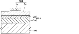
- FIG. 5 is a schematic top view showing an example of a capacitive touch panel sensor.
- the touch panel sensor shown in FIG. 5 has a touch screen 102 for detecting a touch position on one surface of a transparent substrate 101, and a transparent electrode 103 that detects a change in capacitance in this region and uses it as an X position coordinate;
- a transparent electrode 104 having Y position coordinates is provided.
- Each of the transparent electrodes 103 and 104 having the X and Y position coordinates includes a lead wire 105 for connecting to a driver element circuit for controlling an electric signal as a touch panel, and the lead wire 105 and the transparent electrodes 103 and 104.
- a connection electrode 106 for connecting the two is disposed. Further, a connection terminal 107 connected to the driver element circuit is disposed at the end of the lead-out wiring 105 opposite to the connection electrode 106.
- FIG. 6 is a schematic diagram showing an example of a manufacturing method of the touch panel sensor shown in FIG.
- the transparent electrodes 103 and 104 are formed by the conductive pattern forming method according to the present invention.
- a transparent electrode (X position coordinate) 103 is formed on a transparent substrate 101.
- the photosensitive conductive film 10 is laminated so that the photosensitive resin layer 3 is connected to the transparent substrate 101.
- the transferred photosensitive layer 4 (the conductive film 2 and the photosensitive resin layer 3) is irradiated with an actinic ray in a desired shape through a light-shielding mask (first exposure step). Thereafter, the light shielding mask is removed, the support film is further peeled off, and the photosensitive layer 4 is irradiated with actinic rays (second exposure step).
- FIG. 6B is a schematic cross-sectional view taken along the line II in FIG.
- FIG. 6D is a schematic cross-sectional view taken along the line II-II in FIG.
- a lead wire 105 for connecting to an external circuit and a connection light bulb 106 for connecting the lead wire and the transparent electrodes 103 and 104 are formed on the surface of the transparent substrate 101 (not shown).
- the lead line 105 and the connection electrode 106 are shown to be formed after the formation of the transparent electrodes 103 and 104, but they may be formed simultaneously with the formation of the transparent electrodes.
- the lead line 105 can be formed at the same time as the connection electrode 106 is formed by screen printing using a conductive paste material containing flaky silver, for example.
- FIGS. 7 and 8 are partial cross-sectional views taken along lines a-a 'and b-b' shown in FIG. 5, respectively. These indicate the intersections of the transparent electrodes at the XY position coordinates.
- the transparent electrode is formed by the conductive pattern forming method according to the present invention, so that a touch panel sensor with small steps and high smoothness can be obtained.
- the (B) component used by the Example and the comparative example is as follows.
- DPHA Nippon Kayaku Co., Ltd., dipentaerythritol hexaacrylate, hydroxyl value 40
- TMPTA Nippon Kayaku Co., Ltd., trimethylolpropane triacrylate, hydroxyl value 0
- PET-30 Nippon Kayaku Co., Ltd., pentaerythritol triacrylate, hydroxyl value 110
- A-9550 manufactured by Shin-Nakamura Chemical Co., Ltd., dipentaerythritol polyacrylate, hydroxyl value 40
- A-9570 manufactured by Shin-Nakamura Chemical Co., Ltd., dipentaerythritol polyacrylate, hydroxyl value 70
- A-TMM-3 made by Shin-Nakamura Chemical Co., Ltd., pentaerythritol triacrylate, hydroxyl value 110
- A-TMM-3LMN manufactured by Shin-Nakamura
- the reaction solution was allowed to stand at 30 ° C. or less, diluted 10-fold with acetone, centrifuged at 2000 rpm for 20 minutes with a centrifuge, and the supernatant was decanted.
- Acetone was added to the precipitate, and after stirring, the mixture was centrifuged under the same conditions as described above, and acetone was decanted. Then, it centrifuged twice using distilled water similarly, and obtained the silver fiber.
- the fiber diameter (diameter) was about 5 nm
- the fiber length was about 5 ⁇ m.
- Weight average molecular weight The weight average molecular weight (Mw) was measured by gel permeation chromatography (GPC), and was derived by conversion using a standard polystyrene calibration curve.
- GPC condition Pump Hitachi L-6000 type (product name, manufactured by Hitachi, Ltd.) Column: Gelpack GL-R420, Gelpack GL-R430, Gelpack GL-R440 (above, manufactured by Hitachi Chemical Co., Ltd., product name)
- Eluent Tetrahydrofuran Measurement temperature: 40 ° C
- Flow rate 2.05 mL / min
- Detector Hitachi L-3300 type RI (manufactured by Hitachi, Ltd., product name)
- the hydroxyl value was measured as follows. First, the binder polymer solution prepared above was heated at 130 ° C. for 1 hour to remove volatile components, thereby obtaining a solid content. Then, after precisely weighing 1 g of the polymer whose hydroxyl value is to be measured, the precisely weighed polymer is put into an Erlenmeyer flask, and 10 mL of 10% by mass acetic anhydride pyridine solution is added and uniformly dissolved, and then at 100 ° C. for 1 hour. Heated. After heating, 10 mL of water and 10 mL of pyridine were added and heated at 100 ° C. for 10 minutes.
- Hydroxyl value (AB) ⁇ f ⁇ 28.05 / sample (g) + acid value (where A represents the amount (mL) of 0.5 mol / L potassium hydroxide ethanol solution used in the blank test). , B represents the amount (mL) of 0.5 mol / L potassium hydroxide ethanol solution used for titration, and f represents a factor.
- Acid value was measured as follows. First, the binder polymer solution prepared above was heated at 130 ° C. for 1 hour to remove volatile components, thereby obtaining a solid content. Then, after precisely weighing 1 g of the polymer whose acid value is to be measured, the precisely weighed polymer was put into an Erlenmeyer flask, 30 g of acetone was added to this polymer, and this was uniformly dissolved. Next, an appropriate amount of an indicator, phenolphthalein, was added to the solution, and titration was performed using a 0.1N aqueous KOH solution. And the acid value was computed by following Formula.
- the coefficient of thermal expansion of the cured film was measured when the temperature was increased at a rate of temperature increase of 5 ° C./min, and the inflection point obtained from the curve was determined as the glass transition temperature Tg. As sought.
- Example 1 ⁇ Preparation of photosensitive conductive film> [Preparation of conductive film (conductive film of photosensitive conductive film)]
- the silver fiber dispersion obtained above was uniformly applied at 25 g / m 2 onto a 50 ⁇ m-thick polyethylene terephthalate film (PET film, product name “G2-50” manufactured by Teijin Limited) as a support film.
- PET film polyethylene terephthalate film
- the film was dried for 3 minutes with a hot air convection dryer at 100 ° C. to form a conductive film.
- the film thickness after drying of the electrically conductive film was about 0.1 micrometer.
- the hydroxyl value of the photosensitive resin composition was measured in the same manner as in the binder polymer solution. The results are shown in Table 6.
- the photosensitive resin composition solution is uniformly applied onto a 50 ⁇ m-thick polyethylene terephthalate (pet) film on which a conductive film is formed with a conductive film, and dried for 10 minutes in a hot air convection dryer at 100 ° C. for photosensitive resin. A layer was formed. Thereafter, the photosensitive resin layer was covered with a protective film made of polyethylene (manufactured by Tamapoly Co., Ltd., trade name “NF-13”) to obtain a photosensitive conductive film. In addition, the film thickness after drying of the photosensitive resin layer was 5 micrometers.
- the visible light transmittance of the obtained sample was measured in a measurement wavelength range of 400 to 700 nm using an ultraviolet-visible spectrophotometer (U-3310) manufactured by Hitachi Instrument Service Co., Ltd.
- the transmittance of the obtained sample was 92% at a wavelength of 700 nm, 91% at a wavelength of 550 nm, and 87% at a wavelength of 400 nm, and good transmittance was secured.
- Silver paste connection reliability test for photosensitive conductive film those in which disconnection failure is unlikely to occur between the photosensitive conductive film and the silver paste under high temperature and high humidity conditions are referred to as “good silver paste connection reliability”, and those in which disconnection failure is likely to occur are referred to as “silver paste”
- the connection reliability is bad.
- a method for checking whether the silver paste connection reliability is good or bad will be referred to as a silver paste connection reliability test.
- a laminator (Toyobo Co., Ltd., trade name A4300, length 12 cm ⁇ width 12 cm, thickness 125 ⁇ m) is laminated so that the photosensitive resin layer is in contact.
- Hitachi Chemical Co., Ltd. (trade name: HLM-3000 type)
- a substrate on which a photosensitive conductive film including a support film was laminated was prepared.
- an exposure amount of 5 ⁇ 10 2 is applied to the photosensitive conductive film on the substrate from the support film side (above the photosensitive conductive film conductive film) using a parallel beam exposure machine (EXM1201 manufactured by Oak Manufacturing Co., Ltd.). After irradiating ultraviolet rays at J / m 2 (measured value at i-line (wavelength 365 nm)), the support film is removed, and the exposure amount is 1 ⁇ 10 4 J / m 2 from above the conductive film of the photosensitive conductive film.
- a parallel beam exposure machine EXM1201 manufactured by Oak Manufacturing Co., Ltd.
- the sheet resistance value of the obtained photosensitive layer solid film was measured with a non-contact resistance measuring device (Napson Co., Ltd., NC-10) and found to be 270 ⁇ 20 ⁇ / ⁇ .
- silver paste electrodes were formed on the obtained photosensitive layer solid film at intervals of 3 cm.
- the silver paste electrode was applied so as to have a diameter of 2 mm and a thickness of 1 mm.
- As silver paste TB3351C (manufactured by Three Bond Co., Ltd.), AF4500 (manufactured by Taiyo Ink Manufacturing Co., Ltd.), AF6100 (manufactured by Taiyo Ink Manufacturing Co., Ltd.), DW-117H-41 (manufactured by Toyobo Co., Ltd.), DW- 250H-5 (Toyobo Co., Ltd.), DW-250H-23 (Toyobo Co., Ltd.), DW-420L-2 (Toyobo Co., Ltd.), FA-301CA (Fujikura Kasei Co., Ltd.), FA -401CA (manufactured by Fujikura Kasei Co., Ltd.) was used, and all silver pastes were coated
- the silver paste connection reliability was evaluated using the obtained silver paste connection reliability evaluation sample.
- the resistance value between the silver paste electrodes formed at intervals of 3 cm was measured using a pocket tester (manufactured by Custom Co., Ltd., CDM-03D).
- the resistance value is 350 to 400 ⁇ , and this resistance value is set as the initial value (R0) before the silver paste connection reliability evaluation.
- the silver paste connection reliability of the photosensitive conductive film was evaluated according to the following ratings based on the resistance values R0 and R1 before and after the reliability evaluation.
- the ratio of R0 to R1 (R1 / R0) was Rr.
- the results are shown in Table 6. ⁇ ; Rr ⁇ 1.1 ⁇ ; 1.1 ⁇ Rr ⁇ 1.25 ⁇ ; 1.25 ⁇ Rr ⁇ 2 ⁇ : Rr> 2 XX; Rr> 2, R1> 1 ⁇ 10 6 ⁇
- Comparative Examples 1-6 Except having used the photosensitive resin composition solution shown in Table 6, the photosensitive conductive film was produced similarly to Example 1, the silver paste connection reliability test was implemented, and the silver paste connection reliability was evaluated. The results are shown in Table 6.
- the photosensitive conductive film of the present invention it is possible to form a conductive pattern that hardly causes disconnection failure with the silver paste even under high temperature and high humidity conditions without depending on the composition of the silver paste.
Landscapes
- Engineering & Computer Science (AREA)
- Physics & Mathematics (AREA)
- General Physics & Mathematics (AREA)
- General Engineering & Computer Science (AREA)
- Theoretical Computer Science (AREA)
- Spectroscopy & Molecular Physics (AREA)
- Human Computer Interaction (AREA)
- Chemical & Material Sciences (AREA)
- Chemical Kinetics & Catalysis (AREA)
- Materials For Photolithography (AREA)
Abstract
L'invention concerne un film conducteur photosensible qui est équipé d'un film de support, d'une membrane conductrice agencée sur le film de support, et d'une couche de résine photosensible agencée sur la membrane conductrice. Ladite couche de résine photosensible comprend (A) un polymère de liant, (B) un composé photopolymérisable et (C) un initiateur de photopolymérisation. L'indice hydroxyle de la teneur en matière solide de ladite couche de résine photosensible, est inférieur ou égal à 40mgKOH/g.
Applications Claiming Priority (2)
| Application Number | Priority Date | Filing Date | Title |
|---|---|---|---|
| JP2013117878 | 2013-06-04 | ||
| JP2013-117878 | 2013-06-04 |
Publications (1)
| Publication Number | Publication Date |
|---|---|
| WO2014196154A1 true WO2014196154A1 (fr) | 2014-12-11 |
Family
ID=52007815
Family Applications (1)
| Application Number | Title | Priority Date | Filing Date |
|---|---|---|---|
| PCT/JP2014/002770 WO2014196154A1 (fr) | 2013-06-04 | 2014-05-27 | Film conducteur photosensible, procédé de formation de motif conducteur mettant en œuvre celui-ci, et substrat de motif conducteur |
Country Status (2)
| Country | Link |
|---|---|
| TW (1) | TW201502704A (fr) |
| WO (1) | WO2014196154A1 (fr) |
Cited By (2)
| Publication number | Priority date | Publication date | Assignee | Title |
|---|---|---|---|---|
| JP2017133008A (ja) * | 2016-01-26 | 2017-08-03 | 住友化学株式会社 | 着色硬化性樹脂組成物、カラーフィルタ及びそれを含む表示装置 |
| WO2018087816A1 (fr) * | 2016-11-08 | 2018-05-17 | 日立化成株式会社 | Film conducteur photosensible, procédé de formation d'un motif conducteur, et procédé de fabrication de base de motif conducteur |
Citations (6)
| Publication number | Priority date | Publication date | Assignee | Title |
|---|---|---|---|---|
| JPS62139547A (ja) * | 1985-12-13 | 1987-06-23 | Daicel Chem Ind Ltd | 帯電防止性を有する感光積層体 |
| JP2005321716A (ja) * | 2004-05-11 | 2005-11-17 | Mitsui Chemicals Inc | ドライフィルム及びそれを用いた加工品 |
| WO2010021224A1 (fr) * | 2008-08-22 | 2010-02-25 | 日立化成工業株式会社 | Film conducteur photosensible, procédé de fabrication du film conducteur, procédé de formation d'un motif conducteur et substrat de film conducteur |
| JP2010251186A (ja) * | 2009-04-17 | 2010-11-04 | Hitachi Chem Co Ltd | 導電性転写フィルム及びそれを用いた導電性パターンの形成方法 |
| WO2012108220A1 (fr) * | 2011-02-10 | 2012-08-16 | 富士フイルム株式会社 | Stratifié servant à former une pellicule conductrice, procédé servant à former une pellicule conductrice, pellicule conductrice, élément conducteur, panneau tactile, et cellule solaire de type intégré |
| WO2013051516A1 (fr) * | 2011-10-03 | 2013-04-11 | 日立化成株式会社 | Procédé de formation de motif conducteur, substrat à motif conducteur et capteur d'écran tactile |
-
2014
- 2014-05-27 WO PCT/JP2014/002770 patent/WO2014196154A1/fr active Application Filing
- 2014-06-04 TW TW103119300A patent/TW201502704A/zh unknown
Patent Citations (6)
| Publication number | Priority date | Publication date | Assignee | Title |
|---|---|---|---|---|
| JPS62139547A (ja) * | 1985-12-13 | 1987-06-23 | Daicel Chem Ind Ltd | 帯電防止性を有する感光積層体 |
| JP2005321716A (ja) * | 2004-05-11 | 2005-11-17 | Mitsui Chemicals Inc | ドライフィルム及びそれを用いた加工品 |
| WO2010021224A1 (fr) * | 2008-08-22 | 2010-02-25 | 日立化成工業株式会社 | Film conducteur photosensible, procédé de fabrication du film conducteur, procédé de formation d'un motif conducteur et substrat de film conducteur |
| JP2010251186A (ja) * | 2009-04-17 | 2010-11-04 | Hitachi Chem Co Ltd | 導電性転写フィルム及びそれを用いた導電性パターンの形成方法 |
| WO2012108220A1 (fr) * | 2011-02-10 | 2012-08-16 | 富士フイルム株式会社 | Stratifié servant à former une pellicule conductrice, procédé servant à former une pellicule conductrice, pellicule conductrice, élément conducteur, panneau tactile, et cellule solaire de type intégré |
| WO2013051516A1 (fr) * | 2011-10-03 | 2013-04-11 | 日立化成株式会社 | Procédé de formation de motif conducteur, substrat à motif conducteur et capteur d'écran tactile |
Cited By (2)
| Publication number | Priority date | Publication date | Assignee | Title |
|---|---|---|---|---|
| JP2017133008A (ja) * | 2016-01-26 | 2017-08-03 | 住友化学株式会社 | 着色硬化性樹脂組成物、カラーフィルタ及びそれを含む表示装置 |
| WO2018087816A1 (fr) * | 2016-11-08 | 2018-05-17 | 日立化成株式会社 | Film conducteur photosensible, procédé de formation d'un motif conducteur, et procédé de fabrication de base de motif conducteur |
Also Published As
| Publication number | Publication date |
|---|---|
| TW201502704A (zh) | 2015-01-16 |
Similar Documents
| Publication | Publication Date | Title |
|---|---|---|
| JP5257558B1 (ja) | 導電パターンの形成方法、導電パターン基板及びタッチパネルセンサ | |
| JP6402791B2 (ja) | 導電膜基板及びその使用方法 | |
| WO2013151052A1 (fr) | Procédé de formation de motif électroconducteur, et substrat de motif électroconducteur | |
| JP6206028B2 (ja) | 導電パターンの製造方法、その方法により製造された導電パターンを備える導電パターン基板、その導電パターン基板を含むタッチパネルセンサ、及び感光性導電フィルム | |
| WO2016167228A1 (fr) | Film conducteur photosensible, procédé de formation d'un motif conducteur, substrat ayant un motif conducteur, et capteur de panneau tactile | |
| JP6205925B2 (ja) | 感光性導電フィルム、並びにこれを用いた導電パターンの形成方法及び導電パターン基板 | |
| JP5569144B2 (ja) | 感光性導電フィルム、導電膜の形成方法及び導電パターンの形成方法 | |
| JP2016031503A (ja) | 導電パターンの形成方法、導電パターン基板及びタッチパネルセンサ | |
| WO2014196154A1 (fr) | Film conducteur photosensible, procédé de formation de motif conducteur mettant en œuvre celui-ci, et substrat de motif conducteur | |
| JP6399175B2 (ja) | 導電パターンの製造方法、その方法により製造された導電パターンを備える導電パターン基板、その導電パターン基板を含むタッチパネルセンサ、及び感光性導電フィルム | |
| JP2017198878A (ja) | 感光性導電フィルム及びそれを用いた導電パターン、導電パターン基板、タッチパネルセンサの製造方法 | |
| JP2017201350A (ja) | 感光性導電フィルム、導電パターンの形成方法及び導電パターン基板の製造方法 | |
| WO2018008599A1 (fr) | Film conducteur photosensible, procédé de formation de motif conducteur, substrat à motif conducteur et capteur d'écran tactile | |
| JP2018022030A (ja) | 感光性導電フィルム、並びに、これを用いた導電パターンの形成方法、導電パターン基板及びタッチパネルセンサ | |
| JP2017228312A (ja) | 感光性導電フィルム、並びにこれを用いた導電パターンの形成方法及び導電パターン基板 | |
| JP2018040934A (ja) | 感光性導電フィルム、並びにこれを用いた導電パターン基板とその製造方法及びタッチパネルセンサ | |
| JP2017201349A (ja) | 感光性導電フィルム、導電パターンの形成方法及び導電パターン基板の製造方法 | |
| JP2018049054A (ja) | 感光性導電フィルム、導電膜の形成方法、導電パターンの形成方法及び導電膜基板の形成方法 | |
| JP2018139076A (ja) | 感光性導電フィルム及びその製造方法、導電パターンの製造方法、導電パターン基材、並びにタッチパネルセンサ | |
| JP2018116841A (ja) | 導電層付き基材及びその製造方法、並びに、センサ |
Legal Events
| Date | Code | Title | Description |
|---|---|---|---|
| 121 | Ep: the epo has been informed by wipo that ep was designated in this application |
Ref document number: 14807854 Country of ref document: EP Kind code of ref document: A1 |
|
| NENP | Non-entry into the national phase |
Ref country code: DE |
|
| 122 | Ep: pct application non-entry in european phase |
Ref document number: 14807854 Country of ref document: EP Kind code of ref document: A1 |
|
| NENP | Non-entry into the national phase |
Ref country code: JP |