WO2014192255A1 - ラットレース回路、アンテナ装置およびラットレース回路の形成方法 - Google Patents
ラットレース回路、アンテナ装置およびラットレース回路の形成方法 Download PDFInfo
- Publication number
- WO2014192255A1 WO2014192255A1 PCT/JP2014/002668 JP2014002668W WO2014192255A1 WO 2014192255 A1 WO2014192255 A1 WO 2014192255A1 JP 2014002668 W JP2014002668 W JP 2014002668W WO 2014192255 A1 WO2014192255 A1 WO 2014192255A1
- Authority
- WO
- WIPO (PCT)
- Prior art keywords
- line
- lines
- circuit
- rat race
- race circuit
- Prior art date
- Legal status (The legal status is an assumption and is not a legal conclusion. Google has not performed a legal analysis and makes no representation as to the accuracy of the status listed.)
- Ceased
Links
Images




Classifications
-
- H—ELECTRICITY
- H01—ELECTRIC ELEMENTS
- H01P—WAVEGUIDES; RESONATORS, LINES, OR OTHER DEVICES OF THE WAVEGUIDE TYPE
- H01P5/00—Coupling devices of the waveguide type
- H01P5/12—Coupling devices having more than two ports
- H01P5/16—Conjugate devices, i.e. devices having at least one port decoupled from one other port
- H01P5/19—Conjugate devices, i.e. devices having at least one port decoupled from one other port of the junction type
- H01P5/22—Hybrid ring junctions
- H01P5/222—180° rat race hybrid rings
-
- H—ELECTRICITY
- H01—ELECTRIC ELEMENTS
- H01Q—ANTENNAS, i.e. RADIO AERIALS
- H01Q21/00—Antenna arrays or systems
- H01Q21/06—Arrays of individually energised antenna units similarly polarised and spaced apart
- H01Q21/061—Two dimensional planar arrays
- H01Q21/065—Patch antenna array
Definitions
- the present invention relates to a technique related to a circuit configuration constituted by transmission lines.
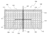
- FIG. 10 schematically shows an example of the antenna device.
- the antenna device 100 includes a first array antenna 101, a second array antenna 102, a ⁇ / ⁇ circuit 103, and transmission lines 105 to 108.
- the first array antenna 101 includes a substrate (for example, a dielectric substrate) 110 and a plurality of radiating elements 111 having a conductor pattern formed on the substrate 110.
- the patterns of the radiating elements 111 have the same shape and the same size, and are arranged on the substrate 110 in a matrix.
- the second array antenna 102 has the same configuration as that of the first array antenna 101 and is juxtaposed with the first array antenna 101. That is, the second array antenna 102 has a configuration in which a plurality of similar radiating elements 112 are arranged in a matrix on a common substrate 110 with the first array antenna 101.
- the transmission line 105 is a line (feeding line) that electrically connects each radiating element 111 of the first array antenna 101 to the ⁇ / ⁇ circuit 103.
- the transmission line 105 has a function of transmitting a received signal (hereinafter also referred to as a received signal S1 of the first array antenna 101) corresponding to the radio wave received by each radiating element 111 to the ⁇ / ⁇ circuit 103.
- the transmission line 106 is a line (feeding line) that electrically connects each radiating element 112 of the second array antenna 102 to the ⁇ / ⁇ circuit 103.
- the transmission line 106 has a function of transmitting a received signal (hereinafter also referred to as a received signal S2 of the second array antenna 102) corresponding to the radio wave received by each radiating element 112 to the ⁇ / ⁇ circuit 103.
- a received signal hereinafter also referred to as a received signal S2 of the second array antenna 102
- the ⁇ / ⁇ circuit 103 is a circuit configuration that combines the reception signal S1 of the first array antenna 101 and the reception signal S2 of the second array antenna 102 in the same phase, and a circuit that combines the reception signals S1 and S2 in the opposite phase.
- the transmission line 107 is a line ( ⁇ port) that outputs from the ⁇ / ⁇ circuit 103 a signal in which the received signals S1 and S2 are combined in phase.
- the transmission line 108 is a line ( ⁇ port) that outputs from the ⁇ / ⁇ circuit 103 a signal in which the reception signals S1 and S2 are combined in reverse phase.
- the antenna device 100 configured as described above is used for radar, for example.
- the antenna device 100 can detect the orientation of the antenna device 100 with respect to a radar detection (tracking) target (target) based on a signal output from the transmission line 108. That is, when the level of the signal output from the transmission line ( ⁇ port) 108 is low, the received signals S1 and S2 of the first array antenna 101 and the second array antenna 102 are in phase or the phases of these received signals. The deviation is small. That is, the first array antenna 101 and the second array antenna 102 are in a state in which they face the radar detection target (target).
- the phase shift between the received signals S1 and S2 between the first array antenna 101 and the second array antenna 102 is large.
- the first array antenna 101 and the second array antenna 102 are in a state of being shifted in the perspective direction with respect to the radar detection target (target object).
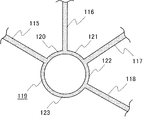
- a rat race circuit as shown in FIG. 13 may be used as the ⁇ / ⁇ circuit 103.
- the rat race circuit is constituted by a line (conductor pattern) formed on the substrate surface of the substrate 110, for example. That is, the rat race circuit has four port lines 115 to 118 functioning as ports (terminals), and a ring-shaped line 119 connected to these port lines 115 to 118 in common.
- the ring-shaped line 119 can be divided into lines 120 to 123.
- the line 120 is a line between connection portions to which the port lines 115 and 116 are connected, respectively.
- the line 121 is a line between connection parts to which the port lines 116 and 117 are respectively connected.
- the line 122 is a line between connection parts to which the port lines 117 and 118 are connected, respectively.
- the line 123 is a line between the connection parts to which the port lines 118 and 115 are respectively connected.
- the line 120 functions as a ⁇ g / 4 line. That is, the line 120 has an electrical length (electric length) corresponding to a quarter of the wavelength ⁇ g of the signals (received signals S1, S2 of the first and second array antennas 101, 102) transmitted through the port line. ).
- the line 121 and the line 122 also function as ⁇ g / 4 lines.
- the line 123 functions as a 3 ⁇ g / 4 line.
- the port line 115 is connected to the transmission line 105 and the port line 117 is transmitted.
- the port line 116 is connected to the transmission line ( ⁇ port) 107
- the port line 118 is connected to the transmission line ( ⁇ port) 108.
- the line 120 between the port lines 115 and 116 and the line 121 between the port lines 116 and 117 have the same line length. For this reason, the reception signal transmitted through the port line 115 and the reception signal transmitted through the port line 117 are combined in phase in the port line 116.
- the line 123 between the port lines 115 and 118 and the line 122 between the port lines 117 and 118 have a line length difference corresponding to a half wavelength ((1/2) ⁇ ⁇ g). For this reason, the reception signal transmitted through the port line 115 and the reception signal transmitted through the port line 117 are combined in the opposite phase in the port line 118.
- Patent Document 1 Japanese Patent Laid-Open No. 2008-005063 relates to a phased array antenna device, and in Patent Document 1, a configuration using a rat race circuit as a circuit for synthesizing signals is shown.
- Japanese Patent Application Laid-Open No. 2012-175329 discloses a configuration in which a rat race circuit is included in a feeding circuit of a phased array antenna.
- Patent Document 3 Japanese Utility Model Publication No. 01-003307) discloses a rat race circuit in which a plurality of rat race circuits are combined.
- Patent Document 4 Japanese Patent Laid-Open No. 2007-013922 describes a configuration in which a filter provided in an antenna feed line is formed by a microstrip line.
- Japanese Patent Application Laid-Open No. 2010-057099 discloses a configuration of a high-frequency transmission / reception circuit related to transmission / reception of signals such as sensors and radars.
- the spacing between the radiating elements tends to be narrow.
- the area in which the ⁇ / ⁇ circuit 103 (rat race circuit) can be formed in the substrate 110 on which the radiating elements are formed is becoming narrower. Therefore, when the radiating elements 111 and 112 and the ⁇ / ⁇ circuit 103 are formed on the same substrate surface (or the same layer) of the substrate 110, the radiating elements 111 and 112 and the ⁇ / ⁇ circuit 103 interfere with each other. I am worried about it.
- the radiating elements 111 and 112 and the ⁇ / ⁇ circuit 103 are formed in different layers of the substrate 110, ⁇ in the radiation direction of the radiating element is considered in consideration of preventing deterioration of the radiation characteristics of the antenna.
- the formation region of the / ⁇ circuit 103 preferably does not overlap.
- the ⁇ / ⁇ circuit 103 (rat race circuit) on a substrate different from the substrate 110 (the ⁇ / ⁇ circuit 103 is a separate component).
- the ⁇ / ⁇ circuit 103 (the rat race circuit, which is a separate component, is connected to the transmission lines 105 and 106 formed on the substrate 110 by a coaxial connector.
- the ⁇ / ⁇ circuit 103 is A measure may be considered in which the ⁇ / ⁇ circuit 103 (magic T) is formed on a substrate surface of the substrate 110 opposite to the surface on which the radiation elements 111 and 112 are formed, instead of the rat race circuit.
- the present invention has been made to solve the above problems. That is, the main object of the present invention is to cope with the downsizing and thinning of the device while preventing the complicated manufacturing process and cost increase of the device on which the rat race circuit is mounted, and further improving the device performance. It is to provide a circuit configuration technique that can contribute to the above.
- the rat race circuit of the present invention comprises: A ⁇ / 4 line with a conductor pattern having an electrical length corresponding to a quarter of the wavelength ⁇ in the signal to be transmitted; A 3 ⁇ / 4 line with a conductor pattern having an electrical length corresponding to three-quarters of the wavelength ⁇ ,
- the three ⁇ / 4 lines and the 3 ⁇ / 4 line are connected in series to form a closed loop, and the 3 ⁇ / 4 line is directed toward the inside of the region surrounded by the closed loop.
- connection portion between the lines forming the closed loop is further connected to a terminal line through which the signal is input and output, and in each connection portion, the ⁇ / connected to the terminal line from the terminal line.
- the extension directions of the lines respectively directed to the four lines or the two lines that are the 3 ⁇ / 4 lines have a configuration that is line symmetric with respect to the center line of the line width in the terminal line.
- the antenna device of the present invention is A plurality of radiating elements formed on a common substrate and having a conductor pattern for transmitting and receiving signals; A circuit for synthesizing a reception signal by the radiating element, The circuit is the rat race circuit of the present invention.
- the method for forming the rat race circuit of the present invention comprises: Three ⁇ / 4 lines with a conductor pattern having an electrical length corresponding to a quarter of the wavelength ⁇ in the signal to be transmitted, and an electrical length corresponding to the three quarters of the wavelength ⁇
- a 3 ⁇ / 4 line with a conductor pattern with a closed loop by being connected in series The 3 ⁇ / 4 line has a line part that enters toward the inner side of the region surrounded by the closed loop, and the line part is open on the entry side and wider on the back side than the opening interval.
- a terminal line for inputting and outputting the signal is further connected, and the ⁇ / 4 line or the 3 ⁇ / 4 line connected from the terminal line to the terminal line.
- the extending directions of the lines respectively facing the two lines are line symmetric with the center line of the line width in the terminal line as the symmetric center line.
- the present invention can cope with the downsizing and thinning of the device while preventing the complicated manufacturing process and cost increase of the device (for example, antenna device) on which the rat race circuit is mounted, and further improving the device performance. Can contribute.
- FIG. 10 is a model diagram showing still another embodiment of the incorporation mode in which the rat race circuit is incorporated in the antenna device. It is a model figure explaining a rat race circuit.
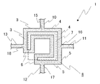
- FIG. 1A is a model diagram showing a rat race circuit according to the first embodiment of the present invention.
- the rat race circuit 1 includes three ⁇ / 4 lines 3 to 5, a 3 ⁇ / 4 line 6, and four terminal lines 10 to 13. Note that ⁇ is the wavelength of the signal transmitted through the line.
- the ⁇ / 4 lines 3 to 5 are each formed by a conductor pattern having an electrical length corresponding to a quarter of the wavelength ⁇ in the signal to be transmitted.
- the 3 ⁇ / 4 line 6 is formed of a conductor pattern having an electrical length corresponding to three-quarters of the wavelength ⁇ .
- the 3 ⁇ / 4 line 6 has an incoming line part 7.
- ⁇ / 4 lines 3 to 5 and 3 ⁇ / 4 line 6 are connected in series (continuous) to form a closed loop 8.
- the incoming line portion 7 in the 3 ⁇ / 4 line 6 enters the inside of the region surrounded by the closed loop 8.
- the entry line portion 7 is opened on the entry entry side (see portion A shown in FIG. 1), and the entry back side (see portion B shown in FIG. 1) is wider than the opening interval. It is formed in an annular shape.
- the term “annular” refers to a shape surrounding a certain region, and the incoming line portion 7 is not limited to a circular shape.
- the terminal lines 10 to 13 are lines for inputting signals to the lines 3 to 6 or outputting signals from the lines 3 to 6 (lines to which signals flowing in the lines 3 to 6 are input and output).
- the terminal lines 10 to 13 are connected to the connection portions 15 to 18 of the lines 3 to 6 in a one-to-one relationship.
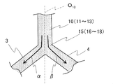
- FIG. 1B is a model diagram showing an enlarged partial region including the connecting portions 15 (16 to 18) in the rat race circuit 1.
- FIG. 1B In each of the connection portions 15 to 18, the extending directions ⁇ and ⁇ directed from the terminal line 10 (11 to 13) to the two lines 3 and 4 connected to the terminal line 10 are center lines of the line width in the terminal line 10. Line symmetry with O 10 as the center line of symmetry.
- the rat race circuit 1 of the first embodiment is configured as described above.
- the rat race circuit 1 can be incorporated in the antenna device 100 as, for example, a ⁇ / ⁇ circuit 103 shown in FIG.
- the lines 3 to 6 and 10 to 13 constituting the rat race circuit 1 are formed on the substrate surface of the substrate 110.
- the terminal line 10 is connected to a transmission line 107 that functions as a ⁇ port
- the terminal line 12 is connected to a transmission line 108 that functions as a ⁇ port.
- the terminal lines 11 and 13 are connected to transmission lines 106 and 105, respectively.
- the radiating elements 111 and 112 may be formed on the substrate surface of the substrate 110, or may be formed on a layer different from the formation surface (formation layer) of the ⁇ / ⁇ circuit 103 on the substrate 110. is there. That is, the layer in which the radiation elements 111 and 112 are formed on the substrate 110 is not limited.
- the received signal of the first array antenna 101 is input through the terminal line 13, and the received signal of the second array antenna 102 is input through the terminal line 11.
- the phase of the reception signal input from the first array antenna 101 to the terminal line 13 and the reception signal input from the second array antenna 102 to the terminal line 11 are in phase.
- the rat race circuit 1 outputs a signal obtained by synthesizing the reception signal of the first array antenna 101 and the reception signal of the second array antenna 102 in phase with each other through the terminal line 10.
- the rat race circuit 1 outputs a signal obtained by synthesizing the reception signals of the first array antenna 101 and the reception signals of the second array antenna 102 in opposite phases through the terminal line 12.
- the rat race circuit 1 according to the first embodiment and the antenna device 100 including the same can obtain the following effects by including the above-described configuration. That is, in the rat race circuit shown in FIG. 13, the area of the ring-shaped line 119 formation area (that is, the area surrounded by the ring-shaped line 119) (hereinafter also referred to as a non-intrusive shape area) is 9 ⁇ ⁇ 2 ⁇ (16 ⁇ ⁇ ) ⁇ 0.179 ⁇ ⁇ 2 .
- the area (hereinafter referred to as a quadrilateral region having the lines 3 to 5 and a part of the line 6 as sides) of the lines 3 to 6 (that is, the following) Can be expressed as ⁇ 2 ⁇ 16 ⁇ 0.0625 ⁇ ⁇ 2 .
- the area of the shape with entry is about one third of the area of the shape without entry shown in FIG.
- the rat race circuit 1 of the first embodiment can be made smaller than the rat race circuit shown in FIG.
- the rat race circuit 1 can be reduced in size, the substrate can be prevented from overlapping with the radiating elements 111 and 112 while avoiding an increase in the size of the substrate 110 of the antenna device 100 (upsizing in the direction in which the substrate surface expands). The effect that it can form in 110 can be acquired. This prevents the problem that the number of layers of the substrate 110 must be increased in order to form the rat race circuit 1, the problem of complication of the manufacturing process of the antenna device 100, and the problem of an increase in cost.
- the two lines 3 connected to the terminal lines 10 (11 to 13) are connected to the terminal lines 10 (11 to 13) as shown in FIG.
- the extending directions ⁇ and ⁇ of 4 are symmetrical with respect to the center line O 10 of the terminal line 10. Therefore, for example, when the received signal of the first array antenna 101 is shunted from the terminal line 13 to the ⁇ / 4 line 3 and the 3 ⁇ / 4 line 6, the received signal is the ⁇ / 4 line 3 and the 3 ⁇ / 4 line. Divide evenly into 6. The same applies to the reception signal of the second array antenna 102, and the reception signal is divided into the ⁇ / 4 line 4 and the 3 ⁇ / 4 line 6 almost equally.
- the rat race circuit 1 can output an accurate signal synthesis result. In other words, if the amount of signal to be synthesized is poor, a situation where the signal level that would have been zero by canceling out the signal would not be canceled out but would be output at a level deviating from zero. To do. Such a situation causes deterioration of the performance of the antenna device 100. On the other hand, the rat race circuit 1 can avoid such a situation because the amount of signals to be synthesized is well balanced. That is, the rat race circuit 1 can improve the performance of the antenna device 100.
- the rat race circuit 1 can cope with the reduction in size and thickness of the antenna device 100 while preventing the manufacturing process of the antenna device 100 from being complicated and the cost from being increased. It can contribute to improvement.
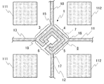
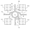
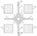
- FIG. 2A is a model diagram showing the rat race circuit 1 of the second embodiment together with the radiation element of the antenna device. Similar to the first embodiment, the rat race circuit 1 of the second embodiment has three ⁇ / 4 lines 3 to 5, a 3 ⁇ / 4 line 6, and four terminal lines 10 to 13. is doing. Further, the 3 ⁇ / 4 line 6 has an incoming line part 7. The incoming line portion 7 has a circular ring shape in the first embodiment, whereas it has a quadrangular ring shape in the second embodiment.
- the rat race circuit 1 of the second embodiment is incorporated as the ⁇ / ⁇ circuit 103 in the antenna device 100 shown in FIG. That is, the lines 3 to 6 and 10 to 13 constituting the rat race circuit 1 are formed on the same substrate surface of the common substrate 110 as the radiation elements 111 and 112 of the antenna device 100. That is, the lines 3 to 6 constituting the closed loop are formed in the gap between the four radiating elements 111 and 112 arranged in a matrix.
- the terminal lines 10 to 13 are formed in a linear manner in the gap between the two radiating elements.
- the radiating elements 111 and 112 have a microstrip line mode.
- Each of the lines 3 to 6 and 10 to 13 of the rat race circuit 1 is also provided with a microstrip line mode, like the radiating elements 111 and 112.
- the terminal line 13 in the rat race circuit 1 is connected to the transmission line 105 of the first array antenna 101, and the terminal line 11 is connected to the transmission line 106 of the second array antenna 102, respectively.
- a received signal input to the terminal line 13 from the first array antenna 101 (transmission line 105) and a received signal input to the terminal line 11 from the second array antenna 102 (transmission line 106). are in phase.
- the signal output from the terminal line 10 is a signal in which the reception signal of the first array antenna 101 and the reception signal of the second array antenna 102 are combined in phase.
- the terminal line 10 is connected to the transmission line ( ⁇ port) 107.
- the signal output from the terminal line 12 is a signal obtained by combining the reception signal of the first array antenna 101 and the reception signal of the second array antenna 102 in opposite phases.
- the terminal line 12 is connected to the transmission line ( ⁇ port) 108.
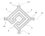
- connection portions 15 to 18 With respect to the connection portions 15 to 18, the interval between adjacent connection portions is equal or substantially equal. Further, as shown in FIG. 2B, the straight line La connecting the connection portions 15 and 17 facing each other and the straight line Lb connecting the connection portions 16 and 18 are orthogonal to each other.
- the rest of the configuration of the rat race circuit 1 of the second embodiment is the same as that of the first embodiment, and a duplicate description thereof is omitted.
- the 3 ⁇ / 4 line 6 has the entry line part 7, and the entry line part 7 is located inside the area surrounded by the closed loop 8. A mode of entering is provided.
- the rat race circuit 1 of 2nd Embodiment can reduce the formation area (occupied area) of the said circuit 1 similarly to 1st Embodiment. Thereby, the rat race circuit 1 can cope with the downsizing and thinning of the antenna device 100 while preventing the manufacturing process of the antenna device 100 in which the circuit 1 is incorporated from being complicated and cost increase.
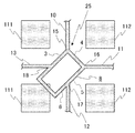
- rat race circuits 25 and 26 show rat race circuits 25 and 26 as comparative examples to be compared with the rat race circuit 1 of the second embodiment, respectively. These rat race circuits 25 and 26 have a mode in which the 3 ⁇ / 4 line 6 does not have the entry line part 7.
- connection portions 15 to 18 are arranged at the same positions as the connection portions 15 to 18 of the rat race circuit 1.
- the 3 ⁇ / 4 line 6 may enter the region where the radiating element 111 is formed. is there. That is, there is a risk that the 3 ⁇ / 4 line 6 and the radiating element 111 interfere with each other.
- each ⁇ / 4 line 3-5 can have an electrical length corresponding to ⁇ / 4
- the 3 ⁇ / 4 line 6 can have an electrical length corresponding to 3 ⁇ / 4.
- the arrangement positions of the connection portions 15 to 18 are set. The arrangement positions of the connection parts 16 to 18 are deviated from the arrangement positions of the connection parts 16 to 18 of the rat race circuit 1. For this reason, the terminal lines 11 to 13 connected to the connection parts 16 to 18 have a portion k that makes a detour toward the connection parts 16 to 18. This part k may interfere with the radiation elements 111 and 112.
- the rat race circuit 1 of the second embodiment can avoid such a problem.
- the rat race circuit 1 of the second embodiment has two lines 3 and 4 connected to the terminal lines 10 (11 to 13) at the connection portions 15 to 18 as shown in FIG. 1B.
- the extending directions ⁇ and ⁇ are symmetrical with respect to the center line O 10 of the terminal line 10.
- the rat race circuit 1 of 2nd Embodiment can also contribute to the improvement of the performance of the antenna apparatus 100 similarly to 1st Embodiment.
- the inventor has confirmed the effect by experiments.
- the inventor outputs an output from the rat race circuit 1 to the transmission line ( ⁇ port) 108 when the rat race circuit 1 of the second embodiment is incorporated as the ⁇ / ⁇ circuit 103 in the antenna device 100. Measuring the signal.
- the present inventor has a transmission line ( ⁇ port) 108 from the rat race circuit 25 when the rat race circuit 25 of the mode shown in FIG. 5 is incorporated in the antenna device 100 as the ⁇ / ⁇ circuit 103. Measure the output signal to.
- the conditions other than the rat race circuit are the same.
- FIG. 3 is a graph showing experimental results when the rat race circuit 1 is incorporated.
- FIG. 4 is a graph showing experimental results when the rat race circuit 25 is incorporated.
- the horizontal axis represents frequency
- the vertical axis represents reflection loss.
- the solid line R is a reflection loss according to the ratio of the signal level (output power) output from the terminal line 10 to the transmission line ( ⁇ port) 108 with respect to the signal level (input power) input to the terminal lines 11 and 13; It represents the relationship with frequency.
- the ⁇ port of the rat race circuit 1 in the communication frequency band (here, 9.4 GHz band) in the antenna device 100 As shown in FIG. 3, by using the rat race circuit 1 of the second embodiment, the ⁇ port of the rat race circuit 1 in the communication frequency band (here, 9.4 GHz band) in the antenna device 100.
- the reflection loss at ⁇ 35 dB is a good result of ⁇ 35 dB or less.
- the reflection loss at the ⁇ port of the rat race circuit 25 is about ⁇ 15 dB.
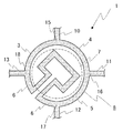
- the rat race circuit 1 may have a shape as shown in FIG. 7 or FIG.
- the straight line connecting the connection portions 15 and 17 facing each other and the straight line connecting the connection portions 16 and 18 are:
- the relationship is orthogonal.
- the interval between adjacent connecting portions is equal or substantially equal.
- the configuration related to the symmetry of the two lines connected to the terminal line is the same as that of the second embodiment.
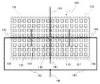
- the rat race circuit 1 may be incorporated in an antenna device 130 as shown in FIG.
- the antenna device 130 includes a first array antenna 131, a second array antenna 132, a third array antenna 133, a fourth array antenna 134, and three ⁇ / ⁇ circuits 135 to 137.
- the antenna device 130 is incorporated in a radar capable of tracking in the azimuth and elevation directions, for example.
- the first to fourth array antennas 131 to 134 have the same configuration as the first and second array antennas 101 and 102 of the antenna device 100.
- the ⁇ / ⁇ circuit 135 has a function of outputting a signal obtained by synthesizing the reception signal of the first array antenna 131 and the reception signal of the second array antenna 132 in phase to the ⁇ / ⁇ circuit 136 through the transmission line 138. Yes. Further, the ⁇ / ⁇ circuit 135 has a function of outputting, to the transmission line 142, a signal obtained by combining the reception signals of the first array antenna 131 and the reception signals of the second array antenna 132 in opposite phases.
- the ⁇ / ⁇ circuit 137 has a function of outputting a signal obtained by synthesizing the reception signal of the third array antenna 133 and the reception signal of the fourth array antenna 134 in phase to the ⁇ / ⁇ circuit 136 through the transmission line 139. Yes. Further, the ⁇ / ⁇ circuit 137 has a function of outputting, to the transmission line 143, a signal obtained by combining the reception signals of the third array antenna 133 and the reception signals of the fourth array antenna 134 in opposite phases. Signals transmitted through the transmission lines 142 and 143 are combined in the transmission line ( ⁇ port) 144 and output to the outside.
- the ⁇ / ⁇ circuit 136 has a function of outputting a signal obtained by synthesizing output signals from the ⁇ / ⁇ circuits 135 and 137 in the same phase toward the transmission line ( ⁇ port) 140. Further, the ⁇ / ⁇ circuit 136 has a function of outputting a signal obtained by synthesizing the output signals from the ⁇ / ⁇ circuits 135 and 137 in reverse phase toward the transmission line ( ⁇ port) 141.
- the first to fourth array antennas 131 to 134 face the front of the detection target (target). It is.
- the third and fourth array antennas 133 and 134 are detected (targeted) rather than the first and second array antennas 131 and 132. ) Away from or approaching.
- the first and second array antennas 131 and 132 and the third and fourth array antennas 133 and 134 are shifted in the perspective direction with respect to the detection target (target). State.
- the first to fourth array antennas 131 to 134 are in a state of facing the detection target (target).
- the second and fourth array antennas 132 and 134 are detected (targeted) rather than the first and third array antennas 131 and 133. ) Away from or approaching.
- the first and third array antennas 131 and 133 and the second and fourth array antennas 132 and 134 are shifted in the perspective direction with respect to the detection target (target). State.
- the rat race circuit 1 of each of the first and second embodiments can be applied to each of the ⁇ / ⁇ circuits 135 to 137.
- the rat race circuit 1 may be applied to all of the ⁇ / ⁇ circuits 135 to 137, or the rat race circuit 1 may be applied to any one or two of the ⁇ / ⁇ circuits 135 to 137. May be.
- the ⁇ / ⁇ circuits 135 and 137 are directed toward the ⁇ / ⁇ circuit 136, respectively. It is preferable that the level of the output signal is balanced.
- the ⁇ / ⁇ circuits 135 and 137 have the same circuit configuration.
- the rat race circuit 1 is preferably applied to the ⁇ / ⁇ circuit 137 (135).
- the phases of the received signals input from the first and second array antennas 101 and 102 to the terminal lines 11 and 13 of the rat race circuit 1 are the same.
- the terminal line 10 is connected to the transmission line ( ⁇ port) 107 of the antenna device 100
- the terminal line 12 is connected to the transmission line ( ⁇ port) 108 of the antenna device 100.
- the phases of the received signals input to the terminal lines 11 and 13 may be opposite to each other.
- the signal output from the terminal line 10 is a signal obtained by combining the reception signal of the first array antenna 101 and the reception signal of the second array antenna 102 in opposite phases.
- the terminal line 10 is connected to the transmission line ( ⁇ port) 108 as shown in FIG.
- the signal output from the terminal line 12 is a signal obtained by combining the reception signal of the first array antenna 101 and the reception signal of the second array antenna 102 in the same phase.
- the terminal line 12 is connected to the transmission line ( ⁇ port) 107. That is, in the example of FIG. 11, the rat race circuit 1 is incorporated into the antenna device 100 in a mode in which the rat race circuit 1 is half-rotated from the state shown in FIG. 2A.
- the rat race circuit 1 may be incorporated in the antenna device 100 in the form shown in FIG. 12 instead of the form shown in FIG. 11. That is, the form shown in FIG. 12 is a form in which the ⁇ / 4 line 5 and the 3 ⁇ / 4 line 6 shown in FIG. 11 are interchanged. Also in the configuration of FIG. 12, when signals having opposite phases are input to the terminal lines 11 and 13, the signal synthesized in the same phase is transmitted from the terminal line 12 to the transmission line ( ⁇ port) as in FIG. It is output to 107. In addition, a signal synthesized in reverse phase is output from the terminal line 10 to the transmission line ( ⁇ port) 108.
- the rat race circuit 1 functions similarly even if the ⁇ / 4 line 5 and the 3 ⁇ / 4 line 6 are interchanged. From this, when the in-phase signal is input to the terminal lines 11 and 13, the rat race circuit 1 has the ⁇ / 4 lines 5 and 3 ⁇ shown in FIG. 1A, FIG. 2A, FIG. 7 and FIG. / 4 Line 6 may be replaced with the antenna device.
- the rat race circuit of the present invention includes an ⁇ / ⁇ circuit (combining circuit) that constitutes an antenna device capable of transmitting and receiving right-handed circularly polarized wave and left-handed circularly polarized wave, and an antenna device capable of transmitting and receiving linearly polarized waves orthogonal to each other. ). Furthermore, the rat race circuit of the present invention can be applied to devices other than the antenna device.
- the present invention is a technique that can be applied to various devices including an array antenna, and can be developed in various fields.
Landscapes
- Details Of Aerials (AREA)
- Variable-Direction Aerials And Aerial Arrays (AREA)
- Radar Systems Or Details Thereof (AREA)
- Support Of Aerials (AREA)
Abstract
Description
伝送対象の信号における波長λの4分の1に対応する電気的な長さを持つ導体パターンによるλ/4線路と、
前記波長λの4分の3に対応する電気的な長さを持つ導体パターンによる3λ/4線路とを有し、
3本の前記λ/4線路と、前記3λ/4線路とは、一連に接続されることによって、閉ループを形成し、前記3λ/4線路は、その閉ループによって囲まれた領域の内側に向けて入り込む線路部位を有し、当該線路部位は、入り込み入側が開口し、かつ、入り込み奥側が前記開口間隔よりも広がっている領域の縁部に沿うような環状に形成されており、
前記閉ループを形成している前記線路間の各接続部には、前記信号が入出力する端子線路がさらに接続されており、各接続部において、前記端子線路から当該端子線路に接続する前記λ/4線路あるいは前記3λ/4線路である2本の線路にそれぞれ向かう線路の伸長方向は、前記端子線路における線路幅の中心線を対称中心線とした線対称である構成を有している。
共通の基板に形成され信号を送受信する導体パターンによる複数の放射素子と、
前記放射素子による受信信号を合成する回路とを有し、
前記回路は、上記本発明のラットレース回路である。
伝送対象の信号における波長λの4分の1に対応する電気的な長さを持つ導体パターンによる3本のλ/4線路と、前記波長λの4分の3に対応する電気的な長さを持つ導体パターンによる3λ/4線路とは、一連に接続されることによって、閉ループを形成し、
前記3λ/4線路は、その閉ループによって囲まれた領域の内側に向けて入り込む線路部位を有し、当該線路部位は、入り込み入側が開口し、かつ、入り込み奥側が前記開口間隔よりも広がっている領域の縁部に沿うような環状に形成されており、
前記閉ループを形成している前記線路間の各接続部において、前記信号が入出力する端子線路をさらに接続し、当該端子線路から当該端子線路に接続する前記λ/4線路あるいは前記3λ/4線路である2本の線路にそれぞれ向かう線路の伸長方向は、前記端子線路における線路幅の中心線を対称中心線とした線対称である。
図1Aは、本発明に係る第1実施形態のラットレース回路を表すモデル図である。このラットレース回路1は、3本のλ/4線路3~5と、3λ/4線路6と、4本の端子線路10~13とを有している。なお、λは線路を伝送する信号の波長である。
以下に、本発明に係る第2実施形態を説明する。なお、第2実施形態の説明において、第1実施形態と同一の名称部分には同一符号を付し、その共通部分の重複説明は省略する。
なお、この発明は第1と第2実施形態に限定されずに様々な実施の態様を採り得る。例えば、ラットレース回路1は、図7や図8に表されるような形状であってもよい。これら図7および図8においても、第2実施形態と同様に、接続部15~18の配置位置に関し、互いに向かい合う接続部15,17を結ぶ直線と、接続部16,18を結ぶ直線とは、直交する関係となっている。また、隣り合う接続部間の間隔は、等間隔あるいは略等間隔となっている。さらに、端子線路に接続する2本の線路の対称性に関わる構成も、第2実施形態と同様となっている。
3,4,5 λ/4線路
6 3λ/4線路
7 入り込み線路部位
15,16,17,18 接続部
100,130 アンテナ装置
111,112 放射素子
Claims (7)
- 伝送対象の信号における波長λの4分の1に対応する電気的な長さを持つ導体パターンによるλ/4線路と、
前記波長λの4分の3に対応する電気的な長さを持つ導体パターンによる3λ/4線路とを有し、
3本の前記λ/4線路と、前記3λ/4線路とは、一連に接続されることによって、閉ループを形成し、前記3λ/4線路は、その閉ループによって囲まれた領域の内側に向けて入り込む線路部位を有し、当該線路部位は、入り込み入側が開口し、かつ、入り込み奥側が前記開口間隔よりも広がっている領域の縁部に沿うような環状に形成されており、
前記閉ループを形成している前記線路間の各接続部には、前記信号が入出力する端子線路がさらに接続されており、各接続部において、前記端子線路から当該端子線路に接続する前記λ/4線路あるいは前記3λ/4線路である2本の線路にそれぞれ向かう線路の伸長方向は、前記端子線路における線路幅の中心線を対称中心線とした線対称である構成を有しているラットレース回路。 - 隣り合う前記接続部間の間隔は等間隔又は略等間隔である請求項1記載のラットレース回路。
- 前記4つの接続部は、互いに向かい合う2つの接続部間を結ぶ2つの直線が直交するように、配置されている請求項1又は請求項2記載のラットレース回路。
- 前記λ/4線路と前記3λ/4線路は、マイクロストリップ線路である請求項1又は請求項2又は請求項3記載のラットレース回路。
- 共通の基板に形成され信号を送受信する導体パターンによる複数の放射素子と、
前記放射素子による受信信号を合成する回路とを有し、
前記回路は、請求項1乃至請求項4の何れか一つに記載のラットレース回路であるアンテナ装置。 - 前記複数の放射素子は配列配置されており、前記ラットレース回路が前記基板における前記放射素子と同じ基板面あるいは同じ層に形成される場合には、前記ラットレース回路は前記放射素子の形成領域間に形成され、前記ラットレース回路が前記基板における前記放射素子とは異なる層に形成される場合には、前記ラットレース回路は前記基板の層の積層方向に前記放射素子の形成領域とオーバーラップしない領域に形成される請求項5記載のアンテナ装置。
- 伝送対象の信号における波長λの4分の1に対応する電気的な長さを持つ導体パターンによる3本のλ/4線路と、前記波長λの4分の3に対応する電気的な長さを持つ導体パターンによる3λ/4線路とは、一連に接続されることによって、閉ループを形成し、
前記3λ/4線路は、その閉ループによって囲まれた領域の内側に向けて入り込む線路部位を有し、当該線路部位は、入り込み入側が開口し、かつ、入り込み奥側が前記開口間隔よりも広がっている領域の縁部に沿うような環状に形成されており、
前記閉ループを形成している前記線路間の各接続部において、前記信号が入出力する端子線路をさらに接続し、当該端子線路から当該端子線路に接続する前記λ/4線路あるいは前記3λ/4線路である2本の線路にそれぞれ向かう線路の伸長方向は、前記端子線路における線路幅の中心線を対称中心線とした線対称であるラットレース回路の形成方法。
Priority Applications (1)
| Application Number | Priority Date | Filing Date | Title |
|---|---|---|---|
| JP2015519631A JP6065112B2 (ja) | 2013-05-28 | 2014-05-21 | ラットレース回路、アンテナ装置およびラットレース回路の形成方法 |
Applications Claiming Priority (2)
| Application Number | Priority Date | Filing Date | Title |
|---|---|---|---|
| JP2013111948 | 2013-05-28 | ||
| JP2013-111948 | 2013-05-28 |
Publications (1)
| Publication Number | Publication Date |
|---|---|
| WO2014192255A1 true WO2014192255A1 (ja) | 2014-12-04 |
Family
ID=51988307
Family Applications (1)
| Application Number | Title | Priority Date | Filing Date |
|---|---|---|---|
| PCT/JP2014/002668 Ceased WO2014192255A1 (ja) | 2013-05-28 | 2014-05-21 | ラットレース回路、アンテナ装置およびラットレース回路の形成方法 |
Country Status (4)
| Country | Link |
|---|---|
| JP (1) | JP6065112B2 (ja) |
| MY (1) | MY178767A (ja) |
| TW (1) | TWI571000B (ja) |
| WO (1) | WO2014192255A1 (ja) |
Cited By (1)
| Publication number | Priority date | Publication date | Assignee | Title |
|---|---|---|---|---|
| EP3386029A1 (en) * | 2017-04-07 | 2018-10-10 | Honeywell International Inc. | Low dispersion phase shifter based on modified hybrid ring power divider |
Citations (2)
| Publication number | Priority date | Publication date | Assignee | Title |
|---|---|---|---|---|
| US4093928A (en) * | 1976-12-20 | 1978-06-06 | The United States Of America As Represented By The Secretary Of The Navy | Microstrip hybrid ring coupler |
| JP2011142413A (ja) * | 2010-01-05 | 2011-07-21 | Chugoku Electric Power Co Inc:The | 無線通信システム |
Family Cites Families (3)
| Publication number | Priority date | Publication date | Assignee | Title |
|---|---|---|---|---|
| JPS5779713A (en) * | 1980-11-05 | 1982-05-19 | Mitsubishi Electric Corp | Tracking antenna |
| US4356461A (en) * | 1981-01-14 | 1982-10-26 | The Bendix Corporation | Practical implementation of large Butler matrices |
| JP3920061B2 (ja) * | 2001-09-26 | 2007-05-30 | シャープ株式会社 | 局部発振信号分配器およびこれを用いた低雑音コンバータ |
-
2014
- 2014-05-21 MY MYPI2015704313A patent/MY178767A/en unknown
- 2014-05-21 JP JP2015519631A patent/JP6065112B2/ja active Active
- 2014-05-21 WO PCT/JP2014/002668 patent/WO2014192255A1/ja not_active Ceased
- 2014-05-26 TW TW103118325A patent/TWI571000B/zh active
Patent Citations (2)
| Publication number | Priority date | Publication date | Assignee | Title |
|---|---|---|---|---|
| US4093928A (en) * | 1976-12-20 | 1978-06-06 | The United States Of America As Represented By The Secretary Of The Navy | Microstrip hybrid ring coupler |
| JP2011142413A (ja) * | 2010-01-05 | 2011-07-21 | Chugoku Electric Power Co Inc:The | 無線通信システム |
Cited By (2)
| Publication number | Priority date | Publication date | Assignee | Title |
|---|---|---|---|---|
| EP3386029A1 (en) * | 2017-04-07 | 2018-10-10 | Honeywell International Inc. | Low dispersion phase shifter based on modified hybrid ring power divider |
| US10476119B2 (en) | 2017-04-07 | 2019-11-12 | Honeywell International Inc. | Low dispersion phase shifter based on modified hybrid ring power divider |
Also Published As
| Publication number | Publication date |
|---|---|
| JP6065112B2 (ja) | 2017-01-25 |
| TWI571000B (zh) | 2017-02-11 |
| MY178767A (en) | 2020-10-20 |
| JPWO2014192255A1 (ja) | 2017-02-23 |
| TW201513451A (zh) | 2015-04-01 |
Similar Documents
| Publication | Publication Date | Title |
|---|---|---|
| US11196175B2 (en) | Antenna device | |
| JP4996640B2 (ja) | アンテナ装置、レーダ装置 | |
| CN101533961B (zh) | 基于八端口结的共基片多波束天线 | |
| US10003117B2 (en) | Two-port triplate-line/waveguide converter having two probes with tips extending in different directions | |
| JPWO2014045966A1 (ja) | 偏波共用アンテナ | |
| JP2010119045A (ja) | アンテナ装置、レーダ装置 | |
| CN109616764A (zh) | 基片集成间隙波导圆极化天线 | |
| Djerafi et al. | Corrugated substrate integrated waveguide (SIW) antipodal linearly tapered slot antenna array fed by quasi-triangular power divider | |
| JP6456716B2 (ja) | アンテナユニット | |
| CN103107387B (zh) | 具有滤波元件的移相器以及滤波元件和天线 | |
| US10511102B2 (en) | Feeder circuit | |
| JP2013085075A (ja) | アンテナ給電回路 | |
| JP6065112B2 (ja) | ラットレース回路、アンテナ装置およびラットレース回路の形成方法 | |
| US12113300B2 (en) | Doppler motion sensor device with high isolation between antennas | |
| JP6305360B2 (ja) | パッチアンテナ及びアレーアンテナ | |
| KR20150088530A (ko) | 복사 차폐가 가능한 고주파 위상 가변기 | |
| US11289796B2 (en) | Circuit board arrangement for signal supply to a radiator | |
| JP2013034118A (ja) | アレーアンテナ | |
| US20160365646A1 (en) | Array antenna device | |
| TW201947252A (zh) | 都卜勒移動感應裝置 | |
| JPWO2016174930A1 (ja) | 円偏波アンテナおよび姿勢算出装置 | |
| JP2014222831A (ja) | マルチビームアンテナ用給電回路およびそれを備えるマルチビームアンテナ | |
| JP2013179527A (ja) | アレーアンテナ装置 | |
| JP2008244733A (ja) | 平面アレーアンテナ装置とそれを備えた無線通信装置 | |
| WO2020145303A1 (ja) | 伝送線路構造体 |
Legal Events
| Date | Code | Title | Description |
|---|---|---|---|
| 121 | Ep: the epo has been informed by wipo that ep was designated in this application |
Ref document number: 14804353 Country of ref document: EP Kind code of ref document: A1 |
|
| ENP | Entry into the national phase |
Ref document number: 2015519631 Country of ref document: JP Kind code of ref document: A |
|
| NENP | Non-entry into the national phase |
Ref country code: DE |
|
| WWE | Wipo information: entry into national phase |
Ref document number: IDP00201508613 Country of ref document: ID |
|
| 122 | Ep: pct application non-entry in european phase |
Ref document number: 14804353 Country of ref document: EP Kind code of ref document: A1 |