WO2014189073A1 - Charge-transporting thin film - Google Patents
Charge-transporting thin film Download PDFInfo
- Publication number
- WO2014189073A1 WO2014189073A1 PCT/JP2014/063454 JP2014063454W WO2014189073A1 WO 2014189073 A1 WO2014189073 A1 WO 2014189073A1 JP 2014063454 W JP2014063454 W JP 2014063454W WO 2014189073 A1 WO2014189073 A1 WO 2014189073A1
- Authority
- WO
- WIPO (PCT)
- Prior art keywords
- thin film
- charge
- organic
- chirality
- transfer thin
- Prior art date
Links
- IQJWDKONUHOILI-UHFFFAOYSA-N CC(CO)c1cc(-c2cnccc2)cc(-c2cc(-c3cc(C(C)CO)cc(-c4cccnc4)c3)cc(-c3cc(C(C)CO)cc(-c4cccnc4)c3)c2)c1 Chemical compound CC(CO)c1cc(-c2cnccc2)cc(-c2cc(-c3cc(C(C)CO)cc(-c4cccnc4)c3)cc(-c3cc(C(C)CO)cc(-c4cccnc4)c3)c2)c1 IQJWDKONUHOILI-UHFFFAOYSA-N 0.000 description 2
- 0 CCC(C)Oc(cc1C)cc(c2c(C)c(-[n](c3c4cccc3C)c3c4nccc3C)c3C)c1[o]c2c3S(C)(C)S(C)(C)c1cc(OC(C)CC)cc(c2c(C)c(-[n](c3c4cccc3C)c3c4nccc3C)c3C)c1[o]c2c3S(C)(C)[*+] Chemical compound CCC(C)Oc(cc1C)cc(c2c(C)c(-[n](c3c4cccc3C)c3c4nccc3C)c3C)c1[o]c2c3S(C)(C)S(C)(C)c1cc(OC(C)CC)cc(c2c(C)c(-[n](c3c4cccc3C)c3c4nccc3C)c3C)c1[o]c2c3S(C)(C)[*+] 0.000 description 2
- WRQHRNZIAMCYHT-UHFFFAOYSA-N Cc(cnc(-c1ncccc1)c1C)c1-c1c(C)c(-c2c(C)cnc(-c3ncccc3)c2C)c(C)c(-c2c(C)cnc(-c3ncccc3)c2C)c1C Chemical compound Cc(cnc(-c1ncccc1)c1C)c1-c1c(C)c(-c2c(C)cnc(-c3ncccc3)c2C)c(C)c(-c2c(C)cnc(-c3ncccc3)c2C)c1C WRQHRNZIAMCYHT-UHFFFAOYSA-N 0.000 description 2
- VUPYRVUAGLQQPC-UHFFFAOYSA-N C1C=CC(c(cc(C2=CC=CCC2)c(-[n](c(c2c3)ccc3-c(c(-c3ccccc3)ccc3)c3-c3ccccn3)c3c2nccc3)c2-c3ccccc3)c2-[n]2c3cccnc3c3c2ccc(-c(c(-c2ncccc2)ccc2)c2-c2ccccc2)c3)=CC1 Chemical compound C1C=CC(c(cc(C2=CC=CCC2)c(-[n](c(c2c3)ccc3-c(c(-c3ccccc3)ccc3)c3-c3ccccn3)c3c2nccc3)c2-c3ccccc3)c2-[n]2c3cccnc3c3c2ccc(-c(c(-c2ncccc2)ccc2)c2-c2ccccc2)c3)=CC1 VUPYRVUAGLQQPC-UHFFFAOYSA-N 0.000 description 1
- KHRPPIBGXKFBDG-UHFFFAOYSA-N Cc1cc([o]c(cc2C)c3c(C)c2-[n]2c(ccc(-c4cccc(-c5ccc(c(cccc6)c6[n]6-c(cc7c8cc(-[n]9c(cccc%10)c%10c%10c9cccc%10)ccc88)ccc7[n]8-c7cccc8c7[o]c7ccccc87)c6c5)c4)c4)c4c4ccccc24)c3c(C)c1-[n]1c2ccccc2c2c1cccc2 Chemical compound Cc1cc([o]c(cc2C)c3c(C)c2-[n]2c(ccc(-c4cccc(-c5ccc(c(cccc6)c6[n]6-c(cc7c8cc(-[n]9c(cccc%10)c%10c%10c9cccc%10)ccc88)ccc7[n]8-c7cccc8c7[o]c7ccccc87)c6c5)c4)c4)c4c4ccccc24)c3c(C)c1-[n]1c2ccccc2c2c1cccc2 KHRPPIBGXKFBDG-UHFFFAOYSA-N 0.000 description 1
- DOKACKKMGVDKFA-UHFFFAOYSA-N c(cc1)ccc1-c(cc1)cc(c2cc(-c(cccc3)c3-c3ccccc3)ccc22)c1[n]2-c(cc1)cc(c2c3)c1[o]c2ccc3-c(cc1c2ccccc22)ccc1[n]2-c1ccccc1-c1ccccc1 Chemical compound c(cc1)ccc1-c(cc1)cc(c2cc(-c(cccc3)c3-c3ccccc3)ccc22)c1[n]2-c(cc1)cc(c2c3)c1[o]c2ccc3-c(cc1c2ccccc22)ccc1[n]2-c1ccccc1-c1ccccc1 DOKACKKMGVDKFA-UHFFFAOYSA-N 0.000 description 1
- VCSMLIQMKCATGQ-UHFFFAOYSA-N c(cc1)ccc1-c1cccc(-c2ccccn2)c1-c(cc1)cc(c2ncccc22)c1[n]2-c(c(-c1ccccc1)c(c(-c1ccccc1)c1)-[n](c(c2c3)ccc3-c(c(-c3ncccc3)ccc3)c3-c3ccccc3)c3c2nccc3)c1-c1ccccc1 Chemical compound c(cc1)ccc1-c1cccc(-c2ccccn2)c1-c(cc1)cc(c2ncccc22)c1[n]2-c(c(-c1ccccc1)c(c(-c1ccccc1)c1)-[n](c(c2c3)ccc3-c(c(-c3ncccc3)ccc3)c3-c3ccccc3)c3c2nccc3)c1-c1ccccc1 VCSMLIQMKCATGQ-UHFFFAOYSA-N 0.000 description 1
- YVQGIBIEUHGQCK-UHFFFAOYSA-N c(cc1c2c3cccc2)ccc1[n]3-c(cc1)cc(c2c3)c1[o]c2ccc3-c(cc1c2c3cccc2)ccc1[n]3-c1c(c2ccccc2c2c3cccc2)c3ccc1 Chemical compound c(cc1c2c3cccc2)ccc1[n]3-c(cc1)cc(c2c3)c1[o]c2ccc3-c(cc1c2c3cccc2)ccc1[n]3-c1c(c2ccccc2c2c3cccc2)c3ccc1 YVQGIBIEUHGQCK-UHFFFAOYSA-N 0.000 description 1
Images


Classifications
-
- H—ELECTRICITY
- H01—ELECTRIC ELEMENTS
- H01B—CABLES; CONDUCTORS; INSULATORS; SELECTION OF MATERIALS FOR THEIR CONDUCTIVE, INSULATING OR DIELECTRIC PROPERTIES
- H01B1/00—Conductors or conductive bodies characterised by the conductive materials; Selection of materials as conductors
- H01B1/06—Conductors or conductive bodies characterised by the conductive materials; Selection of materials as conductors mainly consisting of other non-metallic substances
- H01B1/12—Conductors or conductive bodies characterised by the conductive materials; Selection of materials as conductors mainly consisting of other non-metallic substances organic substances
- H01B1/121—Charge-transfer complexes
-
- H—ELECTRICITY
- H01—ELECTRIC ELEMENTS
- H01G—CAPACITORS; CAPACITORS, RECTIFIERS, DETECTORS, SWITCHING DEVICES OR LIGHT-SENSITIVE DEVICES, OF THE ELECTROLYTIC TYPE
- H01G9/00—Electrolytic capacitors, rectifiers, detectors, switching devices, light-sensitive or temperature-sensitive devices; Processes of their manufacture
- H01G9/20—Light-sensitive devices
- H01G9/2059—Light-sensitive devices comprising an organic dye as the active light absorbing material, e.g. adsorbed on an electrode or dissolved in solution
-
- H—ELECTRICITY
- H10—SEMICONDUCTOR DEVICES; ELECTRIC SOLID-STATE DEVICES NOT OTHERWISE PROVIDED FOR
- H10K—ORGANIC ELECTRIC SOLID-STATE DEVICES
- H10K85/00—Organic materials used in the body or electrodes of devices covered by this subclass
- H10K85/20—Carbon compounds, e.g. carbon nanotubes or fullerenes
- H10K85/211—Fullerenes, e.g. C60
- H10K85/215—Fullerenes, e.g. C60 comprising substituents, e.g. PCBM
-
- H—ELECTRICITY
- H10—SEMICONDUCTOR DEVICES; ELECTRIC SOLID-STATE DEVICES NOT OTHERWISE PROVIDED FOR
- H10K—ORGANIC ELECTRIC SOLID-STATE DEVICES
- H10K85/00—Organic materials used in the body or electrodes of devices covered by this subclass
- H10K85/30—Coordination compounds
- H10K85/341—Transition metal complexes, e.g. Ru(II)polypyridine complexes
- H10K85/342—Transition metal complexes, e.g. Ru(II)polypyridine complexes comprising iridium
-
- H—ELECTRICITY
- H10—SEMICONDUCTOR DEVICES; ELECTRIC SOLID-STATE DEVICES NOT OTHERWISE PROVIDED FOR
- H10K—ORGANIC ELECTRIC SOLID-STATE DEVICES
- H10K85/00—Organic materials used in the body or electrodes of devices covered by this subclass
- H10K85/60—Organic compounds having low molecular weight
- H10K85/611—Charge transfer complexes
-
- H—ELECTRICITY
- H10—SEMICONDUCTOR DEVICES; ELECTRIC SOLID-STATE DEVICES NOT OTHERWISE PROVIDED FOR
- H10K—ORGANIC ELECTRIC SOLID-STATE DEVICES
- H10K85/00—Organic materials used in the body or electrodes of devices covered by this subclass
- H10K85/60—Organic compounds having low molecular weight
- H10K85/649—Aromatic compounds comprising a hetero atom
- H10K85/654—Aromatic compounds comprising a hetero atom comprising only nitrogen as heteroatom
-
- H—ELECTRICITY
- H10—SEMICONDUCTOR DEVICES; ELECTRIC SOLID-STATE DEVICES NOT OTHERWISE PROVIDED FOR
- H10K—ORGANIC ELECTRIC SOLID-STATE DEVICES
- H10K85/00—Organic materials used in the body or electrodes of devices covered by this subclass
- H10K85/60—Organic compounds having low molecular weight
- H10K85/649—Aromatic compounds comprising a hetero atom
- H10K85/657—Polycyclic condensed heteroaromatic hydrocarbons
- H10K85/6572—Polycyclic condensed heteroaromatic hydrocarbons comprising only nitrogen in the heteroaromatic polycondensed ring system, e.g. phenanthroline or carbazole
-
- H—ELECTRICITY
- H10—SEMICONDUCTOR DEVICES; ELECTRIC SOLID-STATE DEVICES NOT OTHERWISE PROVIDED FOR
- H10K—ORGANIC ELECTRIC SOLID-STATE DEVICES
- H10K85/00—Organic materials used in the body or electrodes of devices covered by this subclass
- H10K85/60—Organic compounds having low molecular weight
- H10K85/649—Aromatic compounds comprising a hetero atom
- H10K85/657—Polycyclic condensed heteroaromatic hydrocarbons
- H10K85/6574—Polycyclic condensed heteroaromatic hydrocarbons comprising only oxygen in the heteroaromatic polycondensed ring system, e.g. cumarine dyes
-
- C—CHEMISTRY; METALLURGY
- C09—DYES; PAINTS; POLISHES; NATURAL RESINS; ADHESIVES; COMPOSITIONS NOT OTHERWISE PROVIDED FOR; APPLICATIONS OF MATERIALS NOT OTHERWISE PROVIDED FOR
- C09K—MATERIALS FOR MISCELLANEOUS APPLICATIONS, NOT PROVIDED FOR ELSEWHERE
- C09K11/00—Luminescent, e.g. electroluminescent, chemiluminescent materials
- C09K11/06—Luminescent, e.g. electroluminescent, chemiluminescent materials containing organic luminescent materials
-
- H—ELECTRICITY
- H10—SEMICONDUCTOR DEVICES; ELECTRIC SOLID-STATE DEVICES NOT OTHERWISE PROVIDED FOR
- H10K—ORGANIC ELECTRIC SOLID-STATE DEVICES
- H10K2101/00—Properties of the organic materials covered by group H10K85/00
- H10K2101/10—Triplet emission
-
- H—ELECTRICITY
- H10—SEMICONDUCTOR DEVICES; ELECTRIC SOLID-STATE DEVICES NOT OTHERWISE PROVIDED FOR
- H10K—ORGANIC ELECTRIC SOLID-STATE DEVICES
- H10K30/00—Organic devices sensitive to infrared radiation, light, electromagnetic radiation of shorter wavelength or corpuscular radiation
- H10K30/30—Organic devices sensitive to infrared radiation, light, electromagnetic radiation of shorter wavelength or corpuscular radiation comprising bulk heterojunctions, e.g. interpenetrating networks of donor and acceptor material domains
-
- H—ELECTRICITY
- H10—SEMICONDUCTOR DEVICES; ELECTRIC SOLID-STATE DEVICES NOT OTHERWISE PROVIDED FOR
- H10K—ORGANIC ELECTRIC SOLID-STATE DEVICES
- H10K50/00—Organic light-emitting devices
- H10K50/10—OLEDs or polymer light-emitting diodes [PLED]
- H10K50/11—OLEDs or polymer light-emitting diodes [PLED] characterised by the electroluminescent [EL] layers
-
- Y—GENERAL TAGGING OF NEW TECHNOLOGICAL DEVELOPMENTS; GENERAL TAGGING OF CROSS-SECTIONAL TECHNOLOGIES SPANNING OVER SEVERAL SECTIONS OF THE IPC; TECHNICAL SUBJECTS COVERED BY FORMER USPC CROSS-REFERENCE ART COLLECTIONS [XRACs] AND DIGESTS
- Y02—TECHNOLOGIES OR APPLICATIONS FOR MITIGATION OR ADAPTATION AGAINST CLIMATE CHANGE
- Y02E—REDUCTION OF GREENHOUSE GAS [GHG] EMISSIONS, RELATED TO ENERGY GENERATION, TRANSMISSION OR DISTRIBUTION
- Y02E10/00—Energy generation through renewable energy sources
- Y02E10/50—Photovoltaic [PV] energy
- Y02E10/542—Dye sensitized solar cells
-
- Y—GENERAL TAGGING OF NEW TECHNOLOGICAL DEVELOPMENTS; GENERAL TAGGING OF CROSS-SECTIONAL TECHNOLOGIES SPANNING OVER SEVERAL SECTIONS OF THE IPC; TECHNICAL SUBJECTS COVERED BY FORMER USPC CROSS-REFERENCE ART COLLECTIONS [XRACs] AND DIGESTS
- Y02—TECHNOLOGIES OR APPLICATIONS FOR MITIGATION OR ADAPTATION AGAINST CLIMATE CHANGE
- Y02E—REDUCTION OF GREENHOUSE GAS [GHG] EMISSIONS, RELATED TO ENERGY GENERATION, TRANSMISSION OR DISTRIBUTION
- Y02E10/00—Energy generation through renewable energy sources
- Y02E10/50—Photovoltaic [PV] energy
- Y02E10/549—Organic PV cells
Definitions
- the present invention relates to a charge transfer thin film having excellent stability.
- an electric field is applied to an electronic device such as an organic electroluminescence element (hereinafter also referred to as “organic EL element”), a solar cell, and an organic transistor to which an electric field is applied, and charge carriers (generic term for electrons and holes) are applied.
- organic EL element organic electroluminescence element
- solar cell solar cell
- organic transistor organic transistor to which an electric field is applied
- charge carriers generator term for electrons and holes
- a charge-transfer thin film containing an organic material that can move the metal is used. Since the functional organic material contained in the charge transfer thin film is required to have various performances, its development has been active recently.
- organic materials such as copper phthalocyanine complex, which are far from organic materials but rather called pigments rather than pigments, have a chemical structure that is rigid and almost insoluble in any solvent, and has been used industrially since ancient times.
- solubility, flexibility, chemical reactivity, compatibility with other materials, etc. that the original organic material should have are sacrificed. This is not what the future organic materials should be.
- Organic materials are basically isolated and rarely used as single molecules. In many cases, organic materials are always aggregates of the same molecules or coexist with different molecules (including dissimilar materials such as metals and inorganic substances). Exists.
- molecular design is basically done in an isolated and single molecule, and an aggressive design with the in mind that multiple molecules coexist.
- a macroscopic stabilization technique that focuses on the molecular assemblies that are formed.
- the performance of the film or object should not change at all.
- the required performance is color, charge transfer, optical performance such as refractive index, etc., but in any case the state of the film or object changes completely. Without it, the performance does not change at all, that is, the durability is infinite.
- Patent Document 1 discloses a metal complex having a specific ligand as a blue phosphorescent compound.
- Patent Documents 2, 3 and 4 it has been reported that high efficiency, long life, and low driving voltage are achieved by using two similar color dopants together (see, for example, Patent Documents 2, 3 and 4).
- the present invention has been made in view of the above-described problems and situations, and a solution to that problem is to provide a charge-transfer thin film that is less susceptible to disturbance.
- a charge-transporting thin film with little change in resistance over time is realized, and one of the secondary effects is to provide a charge-transfer thin film with excellent stability with little change in light emission characteristics over time. That is.
- the magnitude of fluctuation against disturbance that is, the stability of the film
- ⁇ G the magnitude of the change
- ⁇ S entropy change
- It contains at least two kinds of functional organic compounds having the chirality generation site, at least one of which is a metal complex, and has two or more chirality generation sites in the molecule of the metal complex, whereby the metal complex
- the charge transfer thin film according to any one of items 1 to 4, which contains both an enantiomer and a diastereoisomer.
- the functional organic compound has a biaryl structure, and the biaryl structure has a chirality generation site resulting from a biaryl rotation hindrance, whereby the functional organic compound contains an atropisomer.
- the charge-transfer thin film according to any one of items 1 to 6, which is characterized in that
- the charge transfer thin film contains a functional organic compound having the chirality generating site and a volatile organic material having a boiling point of less than 300 ° C. under normal pressure, and the volatile organic material is asymmetric carbon 10.
- the charge-transfer thin film according to any one of items 1 to 9, wherein
- the functional organic compounds contained in the charge transfer thin film all contain a mixture of the respective enantiomers and diastereoisomers, and the boiling point under atmospheric pressure in the charge transfer thin film is less than 300 ° C. 11.
- the present invention uses a functional organic compound having a chirality occurrence site and effectively utilizes the entropy effect. Unlike the conventional case, the structure is intended for a combination that exhibits an effect intentionally, and a very large effect can be obtained.
- the charge transferable thin film of the present invention is a charge transferable thin film containing one or more kinds of functional organic compounds having a chirality generating site, and is a single molecule of the one or more kinds of functional organic compounds.
- the total value for all types of the number of hit chirality occurrence sites is 4 or more.
- the total value of all types of chirality occurrence sites per molecule is in the range of 5 to 15. Further, it contains at least two functional organic compounds having a chirality-generating site, and at least two of them each contain at least one of an enantiomer and a diastereoisomer, It is also preferable that at least two kinds of functional organic compounds having a generation site are contained, and at least one of them contains both enantiomers and diastereoisomers.
- At least two kinds of functional organic compounds having a chirality generation site are contained, at least one of which is a metal complex, and has two or more chirality generation sites in the molecule of the metal complex, whereby the metal complex Preferably contain both enantiomers and diastereoisomers.
- At least two kinds of functional organic compounds having the chirality generating site are contained, and at least two kinds thereof contain both enantiomers and diastereoisomers.
- the functional organic compound has a biaryl structure, and the biaryl structure has a chirality generation site due to a biaryl rotation hindrance, so that the functional organic compound contains an atropisomer. Is preferred.
- At least one of the functional organic compounds having a chirality generation site is a compound that emits light by electric field excitation.
- the compound which light-emits by electric field excitation is the said metal complex.
- the charge transporting thin film contains a functional organic compound having the chirality generating site and a volatile organic material having a boiling point of less than 300 ° C. under normal pressure, and the volatile organic material contains asymmetric carbon. It is preferable to have.
- the functional organic compounds contained in the charge transporting thin film all contain a mixture of the respective enantiomers and diastereoisomers, and the boiling point under atmospheric pressure is 300 ° C. in the charge transporting thin film. It is preferable that less than volatile organic materials coexist, and further the volatile organic materials have asymmetric carbon.
- the charge transfer thin film of the present invention can be suitably included in electronic devices, organic electroluminescence elements, conductive films, organic thin film solar cells, and dye-sensitized solar cells.
- ⁇ is used to mean that the numerical values described before and after it are included as a lower limit value and an upper limit value.
- thermodynamic background related to the technical idea of the present invention will be described.
- UV absorbers are used in color paper for the purpose of preventing light fading of color photographic images.
- a typical example of the ultraviolet absorber is a hydroxyphenylbenzotriazole derivative. In many cases, a plurality of these derivatives are mixed and exist. There are various reasons for this, but the fact that crystallization does not occur during long-term storage is a basic requirement for UV absorbers. It is a possible level. In the following, this phenomenon will be considered thermodynamically.
- the performance of the film or object should not change at all.
- the required performance is color, charge transfer, optical performance such as refractive index, etc., but in any case, the state of the film or object changes completely. Without it, the performance does not change at all, that is, the durability is infinite.
- ⁇ G The stability of a film or an object (here, for the sake of simplicity, it will be described simply as “film” hereinafter) is determined by the change ( ⁇ G) in the Gibbs free energy of the second law of thermodynamics.
- ⁇ G the change in the Gibbs free energy of the second law of thermodynamics.
- ⁇ G can be expressed by the following equation by applying temperature to the change in enthalpy ( ⁇ H) and the change in entropy (T ⁇ S).
- ⁇ G ⁇ H-T ⁇ S
- the essence of the present invention is a technique capable of improving the stability of a film after formation and, as a result, suppressing fluctuations in the physical properties of the film by effectively utilizing the effect of entropy as a means for increasing ⁇ G to minus. It is.
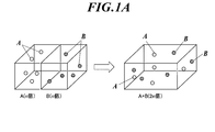
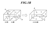
- FIGS. 1A and 1B are schematic diagrams for explaining entropy change when two kinds of gases are mixed.
- nitrogen molecules (component A) and oxygen molecules (component B) are contained at the same density in a box provided with a central portion (see the left side of FIG. 1A).
- oxygen molecules and nitrogen molecules are completely mixed (see the right side of FIG. 1A).
- the enthalpy is considered to be almost zero because both are gasses, but for example, before and after opening the threshold when viewed from the nitrogen molecule, oxygen molecules, which are different molecules, coexist, increasing the randomness. To do. In other words, entropy increases. If the temperature is not absolutely 0 degrees (0 K (Kelvin)), T ⁇ S becomes positive, and ⁇ G becomes negative. That is, the gas is uniformly mixed by the effect of entropy.
- a benzotriazole derivative having a tert-amyl group as a substituent is BT-1 (component A) and BT-2 (component A) has a tert-butyl group.
- FIG. 1A The schematic diagram when BT-1 and BT-2 are mixed and used corresponds to FIG. 1A, and the schematic diagram when the film is formed only by BT-2 corresponds to FIG. 1B.
- a metal complex can be mentioned as the most simple example in which the entropy effect is utilized for stability.
- Table 1 the complex stability of amine complexes of various cadmium measured at room temperature is described as thermodynamic parameters.
- Entropy can also be expressed as the product of the Boltzmann distribution and the number of components. In the case of a chelate complex, it is easy to understand by considering this change in the number of components.
- Konica Photochelate (registered trademark), a chelate dye transfer printing material, has a chelate-forming reaction when a dye with a structure that can be a ligand is diffused and transferred to a metal ion compound in the image receiving layer.
- This is an image forming system in which a chelate dye is formed and fixed, but this formed image dye (chelate complex dye) is not only fixed but also has improved durability and light resistance and heat resistance. Print.
- FIG. 2A and FIG. 2B are examples showing color image fastness using a chelate complex dye.
- 2A and 2B show the changes in the density of cyan, magenta, and yellow dyes represented by C, M, and Y, respectively, as a result of dark fading experiments at 65 ° C.
- FIG. 2A shows the case of Konica photochelation using a chelate complex dye
- FIG. 2B shows the case of general ordinary dye thermal transfer, but the difference is obvious at a glance. You can see that it exists.
- the entropy of the film containing the dye is originally larger at the stage of forming the image, and the entropy effect produces the stability of the film. It can be considered that it meets the requirements.
- a film formed mainly of an organic material can increase the Gibbs free energy in its initial state, and the increase effect is long-term. It can be said that it is large enough to suppress fluctuations even under severe deterioration conditions such as storage at high temperatures.
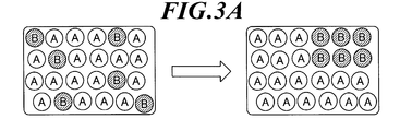
- 3A and 3B are schematic diagrams showing state changes in the charge transport layer or the transportable thin film.
- a molecule having the same function as A and different from A is designated as A 1 and A 2 .
- a 1 and A 2 having the same function but different molecules can be factors that cause randomness in the concept of entropy.
- 3/5 ingredient mixed system of A 1 and A 2 and B as shown in the left Figure 3B because it is large randomness for Figure 3A the left, the free energy of the original Gibbs large negative It will be. Therefore, even if the film as shown in the schematic diagram on the left of FIG. 3B is exposed to the same conditions as when changing from the left of FIG. 3A to the right of FIG. 3A, the state change is mitigated more than the right of FIG. It becomes a state like this.
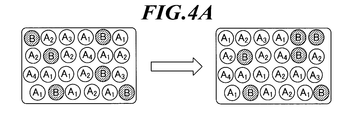
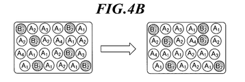
- FIG. 4A left shows that A is four different molecules A 1 , A 2 , A 3 and A 4
- FIG. 4B left shows that B is further formed by two different molecules B 1 and B 2 .
- the increase in the number of components directly contributes to the increase in entropy from the viewpoint of entropy, the stabilization effect becomes great.
- polymer materials are considered to have good film forming properties.
- the film formability can be regarded as the fact that the first thin film is less susceptible to fluctuation over time.
- Polymers take various forms such as distribution of molecular weight, and even if the molecular weight is the same, the shape of the polymer chain is linear, thread-shaped, or bent. That is, when viewed from a certain polymer chain, all the polymer chains present are foreign matters, and the entropy is increased from that viewpoint.
- the enthalpy corresponding to the molecular adsorptive power is considered to be approximate, so the factor that the polymer film-forming property is good is considered to be the entropy effect.
- the polymer itself has a fatal defect that high-purity purification techniques such as recrystallization and sublimation purification cannot be applied.
- the polymer does not follow the physicochemical performance of the repeating unit itself.
- the physical property values which are essential characteristics as a charge transfer thin film such as HOMO and LUMO levels, absorption spectrum and emission spectrum are Since it changes depending on the degree of polymerization and the polymer shape, so-called active molecular design when trying to give a polymer molecule a specific action is more difficult than a low-molecular compound that is a single molecule. .
- low molecular weight compounds can be actively used not only for vapor deposition film formation but also for wet film formation methods such as coating and inkjet.
- the characteristics of low-molecular compounds such as the ease of molecular design, the ease of high-purity purification, and the ease of obtaining major physical properties such as levels and spectra, remain unchanged. This makes it possible to have good film-forming properties of the polymer, that is, to enhance the stability of the film of the charge transfer thin film itself, which matches the ideal form of materials in the near future.
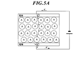
- 5A and 5B are schematic diagrams for explaining hopping movement and recombination in charge movement.
- electric charge (electrons in this figure) is injected from the electrode into the organic material A, hops from A to the existing A, and finally passes the electrons to the counter electrode to become an electron current.
- the principle is the same as this, but the phenomenon of charge recombination is a kind of charge transfer. If holes are seen as shells from which electrons have escaped from molecules, passing electrons to the counter electrode is synonymous with injecting holes from the counter electrode.
- FIG. 5B schematically shows a model in which electrons are injected from the cathode and holes are injected from the anode, and the respective charges recombine on the B molecule.
- B is a luminescent substance, light is emitted when the excited B returns to the ground state. That is, it becomes an organic EL element.
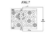
- FIG. 6 is a schematic diagram showing the HOMO (highest occupied molecular orbital) energy level and LUMO (lowest unoccupied molecular orbital) energy level that each molecule of A 1 to A 4 having the function A has independently. It is.
- FIG. 7 is a schematic diagram of a charge recombination thin film formed of four molecules A 1 to A 4 having a function of A and a total of five molecules of B having another function.
- HOMO and LUMO are levels far from the vacuum level (so-called deep levels) on the lower side of the drawing. Electrons injected from the electrode do not enter each of A 1 to A 4 with the same probability, but have the property that they are always injected or localized in a molecule with a deep LUMO level with a high probability. In the hole injection at the anode, holes are injected or localized in a molecule having a shallow HOMO level with a high probability.
- A2 is deep LUMO level than the other three types of molecules
- a 4 is that it is shallow molecular HOMO level than the other three types of molecules.
- FIG. 7 is an organic EL device
- a sufficient amount of excitons of B cannot be obtained unless the amount of electrons and holes is increased to obtain a certain luminance.
- the driving voltage increases. If this state continues, the number of carriers trapped in the carrier trap increases. Since the energy of the trapped carriers is converted into vibration energy that does not participate in light emission, the extra injected electrons and holes eventually consume energy due to the phenomenon of heat generation, and the thin film in which B exists is locally As a result, the temperature of the thin film tends to change. In other words, it is not necessary to simply increase the number of components.
- molecules having a certain function it is an essential condition that molecules of substantially the same level exist.
- the means is to use a functional organic compound having a chirality-generating site, and it is possible to increase ⁇ S and greatly improve the stability of the film without substantially changing the physicochemical properties of the film.
- a functional organic compound having a chirality-generating site Preferably, at least one of an enantiomer (hereinafter also referred to as an enantiomer) and a diastereoisomer (hereinafter also referred to as a diastereomer) is used, and the same function is provided as much as possible.
- an enantiomer hereinafter also referred to as an enantiomer
- a diastereoisomer hereinafter also referred to as a diastereomer
- enantiomers are defined as isomers having the same physicochemical properties other than physiological activity, and diastereomers are isomers having very similar physicochemical properties after that. Inconvenient carrier traps such as those described above can be almost completely defeated.
- the main type having a chirality generating site is the most common carbon atom (or an atom such as nitrogen, sulfur or phosphorus having an unpaired electron) substituted with four different substituents.
- Asymmetric carbon compound (I) molecule having a bond axis (atrop isomerism axis) imparting rotational isomerism such as biaryl group having a bulky substituent at ortho position, so-called axially asymmetric compound (II), aromatic ring Surface chiral compound (III) with chirality generation site due to inability to fix or rotate freely, helicity compound (IV) in which the direction of torsion is defined, such as helicene, and mirror image by forming a complex
- compounds that exhibit asymmetry are also included in the scope of the present invention.
- the octahedral complex with bidentate ligands coordinated is called a delta or lambda body (corresponding to clockwise and counterclockwise propellers).
- Enantiomers also known as mirror images, are isomers that appear when mirrored as in the relationship between the right and left hands, and this applies not only to asymmetric carbon compounds but also to the type (II). Furthermore, (III), (IV) and other substances having a chirality occurrence site are also mirror images of each other, and each can also be called an enantiomer relationship.
- a diastereomer is a molecule that appears when there are two or more chirality occurrence sites, but is not a mirror image but has the same designation when writing a planar molecular structure. It can also be said to be a relationship of mer.
- a complex having a plurality of ligands such as a trivalent hexacoordinate iridium complex
- the resulting complex has a plurality of chiralities. Also expresses diastereomeric isomers.
- the charge transferable thin film of the present invention is a charge transferable thin film containing one or more kinds of functional organic compounds having a chirality generating site, and is a single molecule of the one or more kinds of functional organic compounds.
- the total value for all types of the number of hit chirality occurrence sites is 4 or more.
- a six-conformal facial Ir ortho metal complex has a structure having one chirality generation site and is known as a material for an organic EL thin film.
- the effect of the present invention cannot be exhibited at all by simply including this complex.
- the number of chirality occurrence sites was 2 or 3, although a slight effect was seen, it was not sufficient.
- the effect of the present invention should increase with an increase in the number of chirality occurrence sites, but it is considered that when the number is small, it is easily influenced by other elements when formed as a thin film.
- the total number of chirality occurrence sites is preferably large, preferably 5 or more, more preferably 6 or more, and even more preferably 7 or more.
- the sum of the optically active centers there is no particular upper limit for the sum of the optically active centers, and the larger the number, the more the entropy effect is increased and the levels are substantially the same.
- the charge-transfer thin film refers to a layer (also referred to as an organic functional layer) containing a functional organic compound that can move charge carriers (a general term for electrons and holes) by applying an electric field.
- Such charge transfer thin films are used in electronic devices such as organic EL elements, organic thin film solar cells, dye-sensitized solar cells, and organic thin film transistors.
- the charge transport thin film used in the present invention includes a hole block layer, an electron block layer, an electron injection layer, and a hole injection layer. Can be mentioned.
- the organic EL element may have the layer structure (i) or (ii).
- a layer containing a functional organic compound such as an electron blocking layer may be provided.
- these layer structures of the organic EL element may have a tandem structure (multi-photon structure) in which an organic functional layer is repeatedly formed on the electron injection layer via a charge generation layer.
- Examples of the charge transfer thin film include a hole injection layer, a hole transport layer, an electron blocking layer, a light emitting layer, a hole blocking layer, an electron transport layer, and an electron injection layer.
- Organic photoelectric conversion elements are elements that convert electrical energy into light, and vice versa. Including elements that convert energy, typical examples of the former include light-emitting diodes and semiconductor lasers, and examples of the latter include photodiodes and solar cells.
- a solar cell having a single configuration (a configuration in which the bulk heterojunction layer is one layer) made of a bulk heterojunction type organic photoelectric conversion element may have the following layer structure (i).
- a transparent electrode (anode) In the bulk heterojunction type organic photoelectric conversion element, a transparent electrode (anode), a hole transport layer, a photoelectric conversion part of a bulk hetero junction layer, an electron transport layer, and a counter electrode (cathode) are sequentially laminated on one surface of a substrate. .
- the substrate is a member that holds a transparent electrode, a photoelectric conversion unit, and a counter electrode that are sequentially stacked.
- the substrate can transmit the light subjected to photoelectric conversion, that is, transparent to the wavelength of the light to be photoelectrically converted.
- It is a member.
- a glass substrate or a resin substrate is used as the substrate.
- This substrate is not essential.
- a bulk heterojunction type organic photoelectric conversion element may be formed by forming a transparent electrode and a counter electrode on both surfaces of the photoelectric conversion unit.
- the photoelectric conversion unit is a layer that converts light energy into electrical energy, and includes a bulk heterojunction layer in which a p-type semiconductor material and an n-type semiconductor material are uniformly mixed.
- the p-type semiconductor material functions relatively as an electron donor (donor)
- the n-type semiconductor material functions relatively as an electron acceptor (acceptor).
- the electron donor and the electron acceptor are “an electron donor in which, when light is absorbed, electrons move from the electron donor to the electron acceptor to form a hole-electron pair (charge separation state)”.
- an electron acceptor which does not simply donate or accept electrons like an electrode, but donates or accepts electrons by a photoreaction.
- the generated electric charge is caused by an internal electric field, for example, when the work function of the transparent electrode and the counter electrode is different, due to the potential difference between the transparent electrode and the counter electrode, electrons pass between the electron acceptors, and holes pass between the electron donors, Each is transported to a different electrode and the photocurrent is detected. For example, when the work function of the transparent electrode is larger than the work function of the counter electrode, electrons are transported to the transparent electrode and holes are transported to the counter electrode. If the work function is reversed, electrons and holes are transported in the opposite direction. Moreover, the transport direction of electrons and holes can be controlled by applying a potential between the transparent electrode and the counter electrode.
- the dye-sensitized solar cell can have, for example, the following layer structure (i).
- the sensitizing dye adsorbed on the semiconductor for photoelectric conversion material was irradiated Excites by absorbing light or electromagnetic waves. Electrons generated by excitation move to the semiconductor, and then move to the counter electrode via the conductive support to reduce the redox electrolyte in the charge transfer layer.
- the organic solar cell material (functional organic compound) according to the present invention in which electrons are transferred to a semiconductor is an oxidant, but electrons are supplied from a counter electrode via a charge transfer layer. By this, it is reduced and returns to the original state, and again returns to a state where it can be reduced by electrons supplied from the counter electrode. In this way, electrons flow and a solar cell using a photoelectric conversion element can be configured.
- FIGS. 8A to 8F The structure of the organic thin film transistor is shown in FIGS. 8A to 8F.
- a source electrode 2 and a drain electrode 3 are formed on a support 6 with a metal foil or the like, and a charge transfer thin film (organic A semiconductor layer 1) is formed, an insulating layer 5 is formed thereon, and a gate electrode 4 is further formed thereon to form a field effect transistor.
- FIG. 8B shows the organic semiconductor layer 1 formed between the electrodes in FIG. 8A so as to cover the entire surface of the electrode and the support using a coating method or the like.
- FIG. 8C shows a structure in which the organic semiconductor layer 1 is first formed on the support 6 by using a coating method or the like, and then the source electrode 2, the drain electrode 3, the insulating layer 5, and the gate electrode 4 are formed.
- FIG. 8D after forming the gate electrode 4 with a metal foil or the like on the support 6, the insulating layer 5 is formed, and the source electrode 2 and the drain electrode 3 are formed with the metal foil or the like on the gate electrode 4.
- the organic semiconductor layer 1 formed of the organic thin film transistor material according to the present invention is formed.
- the configuration shown in FIGS. 8E and 8F can be adopted.
- FIG. 9 is a diagram showing an example of a schematic equivalent circuit diagram of an organic TFT sheet.
- the organic TFT sheet 10 has a large number of organic TFTs 11 arranged in a matrix. 7 is a gate bus line of each TFT 11, and 8 is a source bus line of each TFT 11.
- An output element 12 is connected to the source electrode of each TFT 11, and the output element 12 is, for example, a liquid crystal or an electrophoretic element, and constitutes a pixel in the display device.
- the pixel electrode may be used as an input electrode of the photosensor.
- a liquid crystal as an output element is shown by an equivalent circuit composed of a resistor and a capacitor. 13 is a storage capacitor, 14 is a vertical drive circuit, and 15 is a horizontal drive circuit.
- Examples of the conductive sheet include a sheet-like organic EL element, an organic thin film solar cell, a dye-sensitized solar cell, and an organic thin film transistor.
- the functional organic compound according to the present invention is included in the charge transport layer thin film described above. Specific examples include a light emitting dopant, a host compound, a hole transport material, an electron transport material, an organic solar cell material, an organic thin film transistor material, and a solvent. Among these, the functional organic compound according to the present invention is preferably a functional organic compound capable of moving charge carriers (a general term for electrons and holes).
- One or a plurality of types of functional organic compounds having a chirality generation site according to the present invention are contained in a charge transfer thin film, and the number of chirality generation sites per molecule of one or a plurality of types of functional organic compounds.
- the total value for all species is 4 or more.
- the method of counting the species of the functional organic compound is counted as one type in the present invention when the molecules have the same notation when a planar molecular structure is written.
- enantiomers are counted as one type.
- the total value for all species of the number of chirality occurrence sites per molecule is in the range of 5-15.
- At least two kinds of functional organic compounds having a chirality generation site are contained, and at least two of them each represent at least one of an enantiomer and a diastereoisomer. It is preferable to contain. Furthermore, when the functional organic compound contains at least two kinds of functional organic compounds having a chirality generating site and at least one of them has two or more chirality generating sites in the molecule, the functional organic compound is converted into an enantiomer and a diastereoisomer. It is also a preferred embodiment to contain both isomers.
- the functional organic compound has a biaryl structure, and the biaryl structure has a chirality generation site due to a biaryl rotation hindrance, so that the functional organic compound contains an atropisomer.
- having a site where chirality occurs due to rotational disturbance means a site where free rotation of 180 degrees or more at room temperature and normal pressure is inhibited with respect to the bond that forms the rotation axis, and when a molecular model is built It can be defined by a structure that inhibits free rotation of 180 degrees or more with respect to the coupling as the rotation axis.
- Chem-Tutor student modeling system manufactured by SIGMA-ALDRICH can be used.
- an aromatic hydrocarbon derivative, a heteroaromatic hydrocarbon derivative, or the like is preferable, and the functional organic compound includes a total of aromatic rings and / or heteroaromatic rings.
- the functional organic compound includes a total of aromatic rings and / or heteroaromatic rings.
- aromatic hydrocarbon derivatives include benzene, naphthalene, anthracene, tetracene, pentacene, chrysene, and helicene.
- heteroaromatic hydrocarbon derivatives include furan, thiophene, pyrrole, oxazole, thiazole, imidazole, and benzofuran. Benzothiophene, indole, dibenzofuran, dibenzothiophene, carbazole, pyridine, pyrazine, pyrimidine, carboline and the like.
- the content of all the functional organic compounds in the layer containing the functional organic compound having the chirality generating site in the charge transfer thin film is preferably 10% by mass or more, more preferably 20% by mass or more, most preferably Preferably the thing of 50 mass% or more is preferable.
- At least one of the functional organic compounds having a chirality generating site is preferably a compound that emits light by electric field excitation.
- the substance that emits light by electric field excitation is preferably a metal complex.
- Examples of such functional organic compounds include luminescent dopants.
- a fluorescent light emitting dopant or a phosphorescent light emitting dopant can be used, but a phosphorescent light emitting dopant is preferable.
- a phosphorescent luminescent dopant As the luminescent dopant, a phosphorescent luminescent dopant is preferable because high luminous efficiency can be obtained.
- a phosphorescent dopant is a compound in which light emission from an excited triplet is observed, and is a compound having a phosphorescence quantum yield of 0.01 or more at 25 ° C. Preferably it is 0.1 or more.
- phosphorescent dopants There are two types of light emission principles of phosphorescent dopants. One is the recombination of carriers on the host compound to which carriers are transported, generating an excited state of the host compound, and this energy is used as the phosphorescent dopant. It is an energy transfer type in which light emission from a phosphorescent dopant is obtained by moving it. The other is a carrier trap type in which a phosphorescent dopant becomes a carrier trap, and recombination of carriers occurs on the phosphorescent dopant and light emission from the phosphorescent dopant is obtained. In either case, it is a condition that the excited state energy of the phosphorescent dopant is lower than the excited state energy of the host compound.
- the phosphorescent dopant is preferably a metal complex.
- the metal complex include a metal complex having a transition metal as a central metal. Specifically, Cu, Ag, Pd, Rh, Ru, Au, Pt, Ir, Os and the like are preferable, and Cu, Au, Pt are more preferable.
- a metal complex having Ir as a central metal is preferable. Moreover, it is preferable that it has two or more chirality generation
- the functional organic compound having a chirality generating site that is preferably used in the present invention is a light emitting dopant will be exemplified.
- * represents an asymmetric carbon that becomes a chirality generation site
- a bold bond represents a bond axis that is a chirality generation site by inhibiting free rotation
- the host compound is a compound that causes energy transfer or electron transfer from the excited state to the light-emitting compound, and as a result, emits the light-emitting dopant. It also has a function of stably dispersing the light emitting dopant in the light emitting layer.
- the method of stably dispersing the light-emitting molecules for increasing the film density and efficiency with a host compound that improves the lifetime is a trade-off, and simply adjusting the trade-off relationship Even when the intermediate compound was used, there was a limit in performance improvement.
- the host compound according to the present invention stabilization of the light emitting layer is maintained even when the host compound is dense, and both high efficiency and long life can be achieved.
- An electron transport material refers to a material having a function of transporting electrons.
- the charge transfer thin film containing such an electron transport material includes not only an electron transport layer but also an electron injection layer and a hole blocking layer in a broad sense.
- Examples of compounds in the case where the functional organic compound having a chirality generating site, which is preferably used in the present invention, is an electron transport material are shown below.
- the hole transport material refers to a material having a function of transporting holes.
- Such a charge transporting thin film containing a hole transport material includes not only a hole transport layer but also a hole injection layer and an electron blocking layer in a broad sense.
- Examples of compounds in the case where the functional organic compound having a chirality generation site, preferably used in the present invention, is a hole transport material are shown below.
- Organic solar cell materials The compound example in case the functional organic compound which has a chirality generation
- the charge-transfer thin film contains a functional organic compound having a chirality generating site and a volatile organic material having a boiling point of less than 300 ° C. under normal pressure, and the volatile organic material has asymmetric carbon. Is also a preferred embodiment.
- All the functional organic compounds contained in the charge transfer thin film contain a mixture of the respective enantiomers and diastereomers, and the boiling point of the charge transfer thin film under atmospheric pressure is less than 300 ° C. It is also preferred that the materials coexist and that the volatile organic material has asymmetric carbon.
- Examples of the volatile organic material having an asymmetric carbon having a boiling point of less than 300 ° C. under normal pressure that can be used in the present invention include hydrocarbon solvents having illegal carbon, and more preferably aliphatic hydrocarbon solvents.
- Preferred examples include aromatic hydrocarbon solvents and halogen solvents.
- an aliphatic hydrocarbon solvent having an asymmetric carbon and substituted with a substituent acyclic aliphatic hydrocarbon solvent such as hexane and heptane, cycloaliphatic hydrocarbon solvent such as cyclohexane, methanol, ethanol Alcohol solvents such as n-propanol and ethylene glycol, ketone solvents such as acetone and methyl ethyl ketone, ether solvents such as diethyl ether, diisopropyl ether, tetrahydrofuran, 1,4-dioxane and ethylene glycol monomethyl ether), aromatic Examples include hydrocarbon solvents (toluene, xylene, mesitylene, cyclohexylbenzene, isopropylbiphenyl, etc.) and halogen solvents (methylene chloride, 1,1,2-trichloroethane, chloroform, etc.).
- acyclic aliphatic hydrocarbon solvent
- 2-ethylhexane, sec-butyl ether, 2-pentanol, 2-methyltetrahydrofuran, 2-propylene glycol monomethyl ether, 2,3-dimethyl-1,4-dioxane, sec-butylbenzene, 4 -(Sec-butyl) biphenyl, 2-methylcyclohexylbenzene and the like can be mentioned.
- the formation method of the charge transfer thin film of the present invention is not particularly limited, and a conventionally known formation method such as a vacuum deposition method or a wet method (also referred to as a wet process) can be used.
- wet method examples include spin coating method, casting method, ink jet method, printing method, die coating method, blade coating method, roll coating method, spray coating method, curtain coating method, and LB method (Langmuir-Blodgett method). From the viewpoint of obtaining a homogeneous thin film easily and high productivity, a method with high roll-to-roll method suitability such as a die coating method, a roll coating method, an ink jet method and a spray coating method is preferable.
- liquid medium for dissolving or dispersing the functional organic compound according to the present invention examples include ketones such as methyl ethyl ketone and cyclohexanone, fatty acid esters such as ethyl acetate, halogenated hydrocarbons such as dichlorobenzene, toluene, xylene, Aromatic hydrocarbons such as mesitylene and cyclohexylbenzene, aliphatic hydrocarbons such as cyclohexane, decalin, and dodecane, and organic solvents such as DMF and DMSO can be used.
- ketones such as methyl ethyl ketone and cyclohexanone
- fatty acid esters such as ethyl acetate
- halogenated hydrocarbons such as dichlorobenzene, toluene, xylene
- Aromatic hydrocarbons such as mesitylene and cyclohexylbenzene
- a dispersion method it can be dispersed by a dispersion method such as ultrasonic wave, high shearing force dispersion or media dispersion.
- vapor deposition conditions vary depending on the type of compound used, but generally a boat heating temperature of 50 to 450 ° C., a degree of vacuum of 10 ⁇ 6 to 10 ⁇ 2 Pa, and a vapor deposition rate of 0.01 to It is desirable to select appropriately within a range of 50 nm / second, a substrate temperature of ⁇ 50 to 300 ° C., and a film thickness of 0.1 nm to 5 ⁇ m, preferably 5 to 200 nm.
- the formation of the charge transfer thin film of the present invention is preferably made consistently from the hole injection layer to the cathode by a single evacuation, but it may be taken out halfway and subjected to different film forming methods. In that case, it is preferable to perform the work in a dry inert gas atmosphere.
- the film thickness of the charge-transfer thin film of the present invention containing the functional organic compound according to the present invention varies depending on the layer, but can be in the range of 0.1 nm to 5 ⁇ m. It is desirable to select appropriately within the range of 5 to 200 nm.
- an electrode material made of a metal, an alloy, an electrically conductive compound or a mixture thereof having a high work function (4 eV or more, preferably 4.5 V or more) is preferable.
- electrode substances include metals such as Au, and conductive transparent materials such as CuI, ITO (indium tin oxide), SnO 2 , and ZnO.
- conductive transparent materials such as CuI, ITO (indium tin oxide), SnO 2 , and ZnO.
- an amorphous material such as IDIXO (In 2 O 3 —ZnO) capable of forming a transparent conductive film may be used.
- the anode may be formed by depositing a thin film of these electrode materials by vapor deposition or sputtering, and a pattern having a desired shape may be formed by photolithography, or when pattern accuracy is not so high (about 100 ⁇ m or more) A pattern may be formed through a mask having a desired shape at the time of vapor deposition or sputtering of the electrode material.
- a wet film forming method such as a printing method or a coating method can be used.
- the transmittance be greater than 10%, and the sheet resistance as the anode is preferably several hundred ⁇ / ⁇ or less.
- the film thickness of the anode depends on the material, but is usually selected in the range of 10 nm to 1 ⁇ m, preferably 10 to 200 nm.
- cathode As the cathode, a metal having a work function (4 eV or less) metal (referred to as an electron injecting metal), an alloy, an electrically conductive compound, and a mixture thereof is used. Specific examples of such electrode materials include sodium, sodium-potassium alloy, magnesium, lithium, magnesium / copper mixture, magnesium / silver mixture, magnesium / aluminum mixture, magnesium / indium mixture, aluminum / aluminum oxide (Al 2 O 3 ) Mixtures, indium, lithium / aluminum mixtures, aluminum, rare earth metals and the like.
- a mixture of an electron injecting metal and a second metal which is a stable metal having a larger work function than this for example, a magnesium / silver mixture, Magnesium / aluminum mixtures, magnesium / indium mixtures, aluminum / aluminum oxide (Al 2 O 3 ) mixtures, lithium / aluminum mixtures, aluminum and the like are preferred.
- the cathode can be produced by forming a thin film of these electrode materials by a method such as vapor deposition or sputtering.
- the sheet resistance as the cathode is preferably several hundred ⁇ / ⁇ or less, and the film thickness is usually selected in the range of 10 nm to 5 ⁇ m, preferably 50 to 200 nm.
- a transparent or translucent cathode can be produced by producing a conductive transparent material mentioned in the description of the anode on the cathode after producing the above metal with a thickness of 1 to 20 nm.
- Support substrates (hereinafter also referred to as substrates, supports, etc.) that can be used in organic EL devices, organic thin film solar cells, dye-sensitized solar cells, etc., equipped with the charge transfer thin film of the present invention include glass and plastic. There are no particular limitations on the type of the material, and it may be transparent or opaque. In the case of an organic EL element, when taking out light from the support substrate side, the support substrate is preferably transparent. Examples of the transparent support substrate preferably used include glass, quartz, and a transparent resin film. A particularly preferable support substrate is a resin film capable of giving flexibility to the organic EL element.
- polyesters such as polyethylene terephthalate (PET) and polyethylene naphthalate (PEN), polyethylene, polypropylene, cellophane, cellulose diacetate, cellulose triacetate (TAC), cellulose acetate butyrate, cellulose acetate propionate ( CAP), cellulose esters such as cellulose acetate phthalate, cellulose nitrate or derivatives thereof, polyvinylidene chloride, polyvinyl alcohol, polyethylene vinyl alcohol, syndiotactic polystyrene, polycarbonate, norbornene resin, polymethylpentene, polyether ketone, polyimide , Polyethersulfone (PES), polyphenylene sulfide, polysulfones Cycloolefin resins such as polyetherimide, polyetherketoneimide, polyamide, fluororesin, nylon, polymethylmethacrylate, acrylic or polyarylate, Arton (trade name, manufactured by JSR) or Appel (trade name, manufactured by J
- the surface of the resin film may be formed with an inorganic film, an organic film, or a hybrid film of both, and the water vapor permeability (25 ⁇ 0.5 ° C.) measured by a method according to JIS K 7129-1992.
- Relative humidity (90 ⁇ 2)% RH) is preferably 1 ⁇ 10 ⁇ 2 g / (m 2 ⁇ 24 h) or less, and further measured by a method according to JIS K 7126-1987.
- a high barrier film having an oxygen permeability of 1 ⁇ 10 ⁇ 3 cm 3 / (m 2 ⁇ 24 h ⁇ atm) or less and a water vapor permeability of 1 ⁇ 10 ⁇ 5 g / (m 2 ⁇ 24 h) or less.
- the material for forming the barrier film may be any material that has a function of suppressing the entry of elements that cause deterioration of elements such as moisture and oxygen.
- silicon oxide, silicon dioxide, silicon nitride, and the like can be used.
- the method for forming the barrier film is not particularly limited.
- vacuum deposition, sputtering, reactive sputtering, molecular beam epitaxy, cluster ion beam, ion plating, plasma polymerization, atmospheric pressure plasma polymerization A plasma CVD method, a laser CVD method, a thermal CVD method, a coating method, or the like can be used, but an atmospheric pressure plasma polymerization method as described in JP-A-2004-68143 is particularly preferable.
- the opaque support substrate examples include metal plates such as aluminum and stainless steel, films, opaque resin substrates, ceramic substrates, and the like.
- Examples of the sealing means used for sealing the organic EL element, the organic thin film solar cell, the dye-sensitized solar cell and the like provided with the charge transfer thin film of the present invention include a sealing member, an electrode, a support substrate, and the like.
- the method of adhering with an adhesive can be mentioned.
- the sealing member may be a concave plate shape or a flat plate shape.
- transparency and electrical insulation are not particularly limited.
- Specific examples include a glass plate, a polymer plate / film, and a metal plate / film.
- the glass plate include soda-lime glass, barium / strontium-containing glass, lead glass, aluminosilicate glass, borosilicate glass, barium borosilicate glass, and quartz.
- the polymer plate include polycarbonate, acrylic, polyethylene terephthalate, polyether sulfide, and polysulfone.
- the metal plate include those made of one or more metals or alloys selected from the group consisting of stainless steel, iron, copper, aluminum, magnesium, nickel, zinc, chromium, titanium, molybdenum, silicon, germanium, and tantalum.
- a polymer film and a metal film can be preferably used.
- the polymer film has an oxygen permeability measured by a method according to JIS K 7126-1987 of 1 ⁇ 10 ⁇ 3 cm 3 / (m 2 ⁇ 24 h ⁇ atm) or less, and a method according to JIS K 7129-1992. in the measured water vapor transmission rate (25 ⁇ 0.5 ° C., relative humidity (90 ⁇ 2)%) is preferably that of 1 ⁇ 10 -3 g / (m 2 / 24h) or less.
- sealing member For processing the sealing member into a concave shape, sandblasting, chemical etching, or the like is used.
- the adhesive include photocuring and thermosetting adhesives having reactive vinyl groups of acrylic acid oligomers and methacrylic acid oligomers, and moisture curing adhesives such as 2-cyanoacrylates. be able to.
- hot-melt type polyamide, polyester, and polyolefin can be mentioned.
- a cationic curing type ultraviolet curing epoxy resin adhesive can be mentioned.
- a protective film or a protective plate may be provided outside the sealing film or the sealing film on the side facing the support substrate with the organic layer interposed therebetween.
- the mechanical strength is not necessarily high, and thus it is preferable to provide such a protective film and a protective plate.
- the same glass plate, polymer plate / film, metal plate / film, etc. used for the sealing can be used, but the polymer film is light and thin. Is preferably used.
- a display of the obtained impedance on the complex plane with the frequency of the applied voltage signal as a parameter is called a Cole-Cole plot.
- basic transfer functions such as modulus, admittance, and dielectric constant can be obtained.
- transfer function suitable for the purpose of analysis can be selected (see “Impedance Spectroscopy of Organic Electronics Elements” Applied Physics, Vol. 76, No. 11, 2007, 1252-1258).
- a modulus (M) plot in which the reciprocal of the capacitance component is known is employed.
- M-plot since the diameter of the arc portion is approximately the reciprocal of the capacitance of the corresponding layer, it is proportional to the film thickness, so that the film thickness deviation can also be detected.
- an equivalent circuit of the organic electroluminescence element is estimated from the locus of the Cole-Cole plot, and the equivalent circuit is determined by matching the locus of the Cole-Cole plot calculated from the equivalent circuit with the measurement data. It is common.
- the IS measurement can be performed using, for example, a Solartron 1260 type impedance analyzer and a 1296 type dielectric constant measurement interface manufactured by Solartron and superimposing an alternating current of 30 to 100 mVrms (frequency range of 0.1 mHz to 10 MHz) on a DC voltage. .
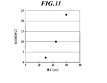
- FIG. 10 is an example of an M-plot with a different thickness of the electron transport layer.
- the vertical axis represents the imaginary part M ′′ (1 / nF), and the horizontal axis represents the real part M ′ (1 / nF).
- FIG. 11 shows the resistance value (R) obtained from this plot plotted against the film thickness of the ETL, and the resistance value at each film thickness can be determined because it is on a substantially straight line.
- FIG. 11 is an example showing the relationship between the ETL film thickness and the resistance value. From the relationship between the ETL film thickness and the resistance value (Resistance) in FIG. 11, the resistance value at each film thickness can be determined because it is on a substantially straight line.
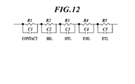
- FIG. 13 shows the result of analyzing each layer using an organic EL element having an element configuration “ITO / HIL / HTL / EML / ETL / Al” as an equivalent circuit model (FIG. 12).
- FIG. 13 is an example showing the resistance-voltage relationship of each layer.
- FIG. 14 shows the respective values at a voltage of 1V.
- FIG. 14 is an example showing an analysis result of the organic EL element after deterioration.
- Example 1 An example in which the charge transfer thin film is a light emitting layer and the functional organic compound is a light emitting dopant and a host compound is shown below.
- polystyrene sulfonate PEDOT / PSS, Bayer, Baytron P Al 4083
- PEDOT / PSS polystyrene sulfonate
- a thin film was formed by spin coating under a condition of 30 seconds and then dried at 200 ° C. for 1 hour to provide a hole injection layer having a thickness of 20 nm.
- This transparent support substrate is fixed to a substrate holder of a commercially available vacuum deposition apparatus, while ⁇ -NPD (4,4′-bis [N- (1-naphthyl) -N-phenylamino] biphenyl) is attached to a resistance heating boat made of molybdenum.
- ⁇ -NPD 4,4′-bis [N- (1-naphthyl) -N-phenylamino] biphenyl
- 200 mg 200 mg
- CBP 4,4′-N, N′-dicarbazolebiphenyl
- compound D-9 was put into another resistance heating boat made of molybdenum.
- 200 mg of BCP (2,9-dimethyl-4,7-diphenyl-1,10-phenanthroline) was placed in a resistance heating boat made of molybdenum, and attached to a vacuum deposition apparatus.
- the vacuum chamber was then depressurized to 4 ⁇ 10 ⁇ 4 Pa, heated by energizing the heating boat containing ⁇ -NPD, and deposited on the hole injection layer at a deposition rate of 0.1 nm / sec.
- the hole transport layer was provided.
- the heating boat containing CBP and the heating boat containing D-9 were energized and heated, and were co-deposited on the hole transport layer at a deposition rate of 0.1 nm / second and 0.010 nm / second, respectively.
- a 40 nm light emitting layer was provided.
- the heating boat containing BCP was energized and heated, and was deposited on the hole blocking layer at a deposition rate of 0.1 nm / second to provide an electron transport layer of 30 nm.
- lithium fluoride 0.5 nm was vapor-deposited as a cathode buffer layer, and aluminum 110 nm was vapor-deposited to form a cathode, whereby an organic EL device 1-1 was produced.
- Organic EL devices 1-2 to 1-52 were prepared in the same manner except that CBP and D-9 were changed to the compounds shown in Table 1 in the production of the organic EL device 1-1.
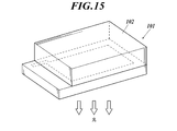
- FIG. 15 shows a schematic diagram of a lighting device, and an organic EL element 101 provided with a charge-transfer thin film of the present invention is covered with a glass cover 102 (note that the sealing operation with the glass cover is an organic EL element). 101 was carried out in a glove box under a nitrogen atmosphere (in an atmosphere of high-purity nitrogen gas having a purity of 99.999% or more) without being exposed to the air.
- a nitrogen atmosphere in an atmosphere of high-purity nitrogen gas having a purity of 99.999% or more
- an epoxy photo-curing adhesive (Luxtrac LC0629B manufactured by Toagosei Co., Ltd.) is applied as a sealant around the glass cover side where the glass cover and the glass substrate on which the organic EL element is manufactured contact, This was stacked on the cathode side and brought into close contact with the transparent support substrate, and the portion excluding the organic EL element from the glass substrate side was irradiated with UV light and cured.
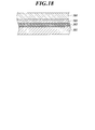
- FIG. 16 shows a cross-sectional view of the lighting device.
- 105 denotes a cathode
- 106 denotes an organic EL layer
- 107 denotes a glass substrate with a transparent electrode.
- the glass cover 102 is filled with nitrogen gas 108 and a water catching agent 109 is provided.
- the organic EL element was measured for the resistance value of the light emitting layer before and after driving for 1000 hours under room temperature (25 ° C.) and constant current conditions of 2.5 mA / cm 2 , and the calculation results are shown below.
- the change rate of the resistance value was obtained by calculation.
- Table 3 shows the relative ratio when the rate of change of the resistance value of the organic EL element 1-1 is 100.
- Rate of change of half width before and after driving
- a value closer to 0 indicates a smaller change rate before and after driving.
- the organic EL elements 1-4 to 1-52 having the charge transfer thin film of the present invention have a resistance value and light emission of the light emitting layer as compared with the organic EL elements 1-1 to 1-3 of the comparative example. Since it was shown that the change rate of the half width of the spectrum was small, an organic EL device having a small change in physical properties of the thin film of the light emitting layer could be obtained.
- Example 2 Other examples in which the charge transfer thin film is a light emitting layer and the functional organic compound is a light emitting dopant and a host compound are shown below.
- PEDOT / PSS poly(3,4-ethylenedioxythiophene) -polystyrene sulfonate
- a thin film was formed by spin coating under a condition of 30 seconds, and then dried at 200 ° C. for 1 hour to provide a first hole transport layer having a thickness of 20 nm.
- This substrate was transferred to a nitrogen atmosphere, and 50 mg of ADS254BE (poly-N, N′-bis (4-butylphenyl) -N, N′-bis (phenyl) benzidine: American on the first hole transport layer: A thin film was formed by spin coating using a solution of Dye Source, Inc. dissolved in 10 ml of monochlorobenzene under conditions of 2500 rpm and 30 seconds. Furthermore, it vacuum-dried at 130 degreeC for 1 hour, and the 2nd positive hole transport layer was formed.
- ADS254BE poly-N, N′-bis (4-butylphenyl) -N, N′-bis (phenyl) benzidine
- a thin film was formed by spin coating using a solution of Dye Source, Inc. dissolved in 10 ml of monochlorobenzene under conditions of 2500 rpm and 30 seconds. Furthermore, it vacuum-dried at 130 degreeC for 1 hour, and the 2nd positive hole transport layer was formed.
- a thin film was formed by spin coating under a condition of 1000 rpm for 30 seconds using a solution of 100 mg CBP and 13 mg D-9 dissolved in 10 ml butyl acetate. Furthermore, it vacuum-dried at 60 degreeC for 1 hour, and was set as the light emitting layer with a film thickness of about 45 nm.
- a thin film was formed on the light emitting layer by spin coating under a condition of 1000 rpm for 30 seconds using a solution in which 50 mg of BCP was dissolved in 10 ml of hexafluoroisopropanol (HFIP). Furthermore, it vacuum-dried at 60 degreeC for 1 hour, and was set as the electron carrying layer with a film thickness of about 25 nm.
- HFIP hexafluoroisopropanol
- this substrate was fixed to a substrate holder of a vacuum deposition apparatus, and after the vacuum chamber was depressurized to 4 ⁇ 10 ⁇ 4 Pa, 0.4 nm of potassium fluoride was deposited as a cathode buffer layer, and further 110 nm of aluminum was deposited. Thus, a cathode was formed to produce an organic EL element 2-1.
- Organic EL elements 2-2 to 2-52 were prepared in the same manner except that CBP and D-9 were changed to the compounds shown in Table 2 in the production of the organic EL element 2-1.
- the organic EL elements 2-4 to 2-52 provided with the charge transfer thin film of the present invention have a resistance value and light emission of the light emitting layer as compared with the organic EL elements 2-1 to 2-3 of the comparative example. Since it was shown that the change rate of the half width of the spectrum was small, an organic EL device having a small change in physical properties of the thin film of the light emitting layer could be obtained.
- Example 3 Other examples in which the charge transfer thin film is a light emitting layer and the functional organic compound is a light emitting dopant and a host compound are shown below.
- This transparent support substrate is fixed to a substrate holder of a commercially available vacuum deposition apparatus, and TPD (N, N′-bis (3-methylphenyl) -N, N′-diphenyl- [1,1′-] is attached to a molybdenum resistance heating boat.
- the pressure in the vacuum chamber was reduced to 4 ⁇ 10 ⁇ 4 Pa, and the heating boat containing TPD was heated by energization, and deposited on a transparent support substrate at a deposition rate of 0.1 nm / second to form a 10 nm hole transport layer.
- the heating boat containing TPD was heated by energization, and deposited on a transparent support substrate at a deposition rate of 0.1 nm / second to form a 10 nm hole transport layer.
- the heating boat containing CBP, D-9, D-1, and D-6 was energized and heated, and the deposition rates were 0.1 nm / second, 0.025 nm / second, 0.0007 nm / second, and 0.005 nm, respectively.
- a 60 nm light emitting layer was provided by co-evaporation on the hole transport layer at 0002 nm / second.
- the heating boat containing BCP was energized and heated, and deposited on the light emitting layer at a deposition rate of 0.1 nm / second to provide a 20 nm electron transport layer.
- Organic EL devices 3-2 to 3-52 were prepared in the same manner except that CBP and D-9 were changed to the compounds shown in Table 5 in the production of the organic EL device 3-1.
- the organic EL elements 3-4 to 3-52 equipped with the charge transfer thin film of the present invention showed a change in the resistance value of the light emitting layer compared to the organic EL elements 3-1 to 3-3 of the comparative example. Since it was shown that the rate was small, an organic EL device having a small change in physical properties of the thin film of the light emitting layer could be obtained.
- Example 4 Other examples in which the charge transfer thin film is a light emitting layer and the functional organic compound is a light emitting dopant and a host compound are shown below.
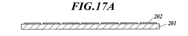
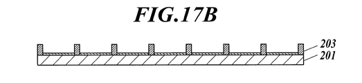
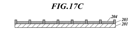
- FIGS. 17A to 17E are schematic configuration diagrams of an organic EL full-color display device. After patterning at a pitch of 100 ⁇ m on a substrate (NH45 manufactured by NH Techno Glass Co., Ltd.) having a 100 nm thick ITO transparent electrode (202) formed on a glass substrate 201 as an anode, non-between the ITO transparent electrodes on this glass substrate.
- a photosensitive polyimide partition 203 (width 20 ⁇ m, thickness 2.0 ⁇ m) was formed by photolithography.
- a hole injection layer composition having the following composition is ejected and injected between polyimide partition walls on the ITO electrode using an inkjet head (manufactured by Epson Corporation; MJ800C), and a hole having a film thickness of 40 nm is obtained by drying at 200 ° C. for 10 minutes.
- An injection layer 204 was produced.
- the following blue light emitting layer composition, green light emitting layer composition and red light emitting layer composition are similarly ejected and injected using an inkjet head, and the respective light emitting layers (205B, 205G, 205R) are injected. ) was formed.
- Al (206) was vacuum-deposited as a cathode so as to cover the light emitting layer 205, and the organic EL element 4-1 was produced.
- the produced organic EL elements 4-1 and 4-2 showed blue, green, and red light emission by applying a voltage to each electrode, and it was found that they could be used as a full-color display device.
- organic EL devices produced using compounds D-102 to D-130 instead of compound D-101 can also be used as a full-color display device.
- the organic EL element 4-2 using a volatile organic material having asymmetric carbon together with a functional organic compound having a chirality generation site is not suitable. It can be seen that the organic EL element 4-1 which does not use a volatile organic material having homogeneous carbon is more stable.
- Example 5 An example in which the charge transporting thin film is an electron transport layer and the functional organic compound is an electron transport material is shown below.
- Organic EL elements 5-1 to 5-15 were similarly prepared except that BCP was changed to the compounds shown in Table 6 in the preparation of organic EL element 1-1.
- the organic EL elements 5-4 to 5-15 equipped with the charge transfer thin film of the present invention have a resistance value of the electron transport layer as compared with the organic EL elements 5-1 to 5-3 of the comparative example. Since it was shown that the rate of change was small, an organic EL device having a small change in physical properties of the thin film of the electron transport layer could be obtained.
- Example 6 An example in which the charge transporting thin film is a hole transport layer and the functional organic compound is a hole transport material is shown below.
- Organic EL elements 6-1 to 6-16 were prepared in the same manner as in the production of the organic EL element 1-1 except that ⁇ -NPD was changed to the compounds shown in Table 7.
- the organic EL elements 6-4 to 6-16 provided with the charge transfer thin film of the present invention have a resistance value of the hole transport layer compared to the organic EL elements 6-1 to 6-3 of the comparative example. It was shown that the rate of change in the thickness of the organic EL device was small, so that an organic EL device with a small change in physical properties of the thin film of the hole transport layer could be obtained.
- Example 7 Provide of organic photoelectric conversion element ⁇ An example in which the charge transfer thin film is a photoelectric conversion layer and the functional organic compounds are C-101 to C-104 is shown below.
- a transparent electrode was formed by patterning an indium tin oxide (ITO) transparent conductive film deposited on a glass substrate to a width of 2 mm using a normal photolithography technique and hydrochloric acid etching.
- ITO indium tin oxide
- the patterned transparent electrode was cleaned in the order of ultrasonic cleaning with a surfactant and ultrapure water, followed by ultrasonic cleaning with ultrapure water, dried by nitrogen blowing, and finally subjected to ultraviolet ozone cleaning.
- Baytron P4083 manufactured by Starck Vitec, which is a conductive polymer, was spin-coated with a film thickness of 60 nm, and then dried by heating at 140 ° C. for 10 minutes in the air.
- the substrate was brought into the glove box and worked in a nitrogen atmosphere.
- the substrate was heat-treated at 140 ° C. for 10 minutes in a nitrogen atmosphere.
- PCPDTBT Natural Mat. Vol. 6 (2007), polythiophene copolymer described in p497) as a p-type semiconductor material on chlorobenzene and PCBM (manufactured by Frontier Carbon, NANOM SPECTRA as an n-type semiconductor material) E100H) and 2.0% by mass of 1,8-octanedithiol were dissolved in the solution, spin-coated at 1200 rpm for 60 seconds while being filtered through a 0.45 ⁇ m filter, And dried for 30 minutes to obtain a photoelectric conversion layer.
- PCPDTBT Natural Mat. Vol. 6 (2007), polythiophene copolymer described in p497
- PCBM manufactured by Frontier Carbon, NANOM SPECTRA as an n-type semiconductor material
- the substrate on which the organic functional layer was formed was placed in a vacuum evaporation apparatus.
- the element was set so that the shadow mask with a width of 2 mm was orthogonal to the transparent electrode, and the inside of the vacuum deposition apparatus was depressurized to 10 ⁇ 3 Pa or less, and then 0.5 nm of lithium fluoride and 80 nm of Al were evaporated.
- the heating for 30 minutes was performed at 120 degreeC, and the organic photoelectric conversion element 1 of the comparative example was obtained.
- the vapor deposition rate was 2 nm / second for all, and the size was 2 mm square.
- organic photoelectric conversion element 1 was sealed with an aluminum cap and a UV curable resin (manufactured by Nagase ChemteX Corporation, UV RESIN XNR5570-B1) in a nitrogen atmosphere. This was designated as organic photoelectric conversion element 7-1.
- Organic photoelectric conversion elements 7-2 to 7-5 were produced in the same manner except that PCBM in the organic photoelectric conversion element 7-1 was changed to the compounds shown in Table 8.
- Example 8 An example in which the charge transfer thin film is a photosensitive layer and the functional organic compounds are C-201 to C-205 is shown below.
- titanium tetraisopropoxide (first grade, manufactured by Wako Pure Chemical Industries, Ltd.) was dropped into 375 ml of pure water over 10 minutes with vigorous stirring at room temperature (a white precipitate was formed), and then 70% aqueous nitric acid was added. After 2.65 ml was added and the reaction system was heated to 80 ° C., stirring was continued for 8 hours. Further, the reaction mixture was concentrated under reduced pressure until the volume of the reaction mixture became about 200 ml, and then 125 ml of pure water and 140 g of titanium oxide powder (Super Titania F-6 manufactured by Showa Titanium Co., Ltd.) were added thereto to obtain a titanium oxide suspension (about 800 ml). ) was prepared. The titanium oxide suspension is applied onto a transparent conductive glass plate coated with fluorine-doped tin oxide, dried naturally and then fired at 300 ° C. for 60 minutes to form a film-like titanium oxide on the support. did.
- a solution in which 5 g of compound R1 is dissolved in 200 ml of methanol solution is prepared, the above-mentioned film-like titanium oxide (semiconductor layer for photoelectric conversion material) is immersed together with the support, and further 1 g of trifluoroacetic acid is added thereto for 2 hours. Irradiated. After the reaction, the film-like titanium oxide (semiconductor layer for photoelectric conversion material) was washed with chloroform and vacuum dried to prepare a photosensitive layer 302 (semiconductor for photoelectric conversion material).
- the counter electrode 304 a transparent conductive glass plate coated with fluorine-doped tin oxide and further carrying platinum thereon is used, and the volume ratio is 1 between the conductive support 301 and the counter electrode 304.
- the charge transfer layer 303 was produced to produce a photoelectric conversion element R1.
- Dye-sensitized solar cells 8-2 to 8-6 were prepared in the same manner except that compound R1 was changed to the compounds shown in Table 9 in dye-sensitized solar cell 8-1.
- the functional organic compound according to the present invention is obtained by irradiating the organic photoelectric conversion element produced above with 100 mW / cm 2 of solar simulator (AM1.5G filter) for 1000 hours in the same manner as in Example 1.
- the dye-sensitized solar cell provided with the charge transfer thin film of the present invention has a value significantly lower than that of the comparative example as shown in Table 9. It was confirmed that
- Example 9 An example in which the charge transfer thin film is a light emitting layer and the functional organic compounds are F-101 to F-118 is shown below.
- Organic EL devices 9-1 to 9-18 were prepared in the same manner except that D-9 was changed to the compounds shown in Table 10 in the production of the organic EL device 1-1.
- the organic EL elements 9-5 to 9-18 equipped with the charge-transfer thin film of the present invention showed a change in the resistance value of the light emitting layer compared to the organic EL elements 9-1 to 9-4 of the comparative examples. Since it was shown that the rate was small, an organic EL device having a small change in physical properties of the thin film of the light emitting layer could be obtained.
- the state change of the charge transfer membrane can be used as it is by applying a new non-destructive measurement method called impedance spectroscopy, and the phenomenon occurring therein can be compared as a resistance value. did it.
- impedance spectroscopy a new non-destructive measurement method
- the magnitude of the error cannot be specifically identified, but it is formed from a mixture of enantiomers and diastereoisomers having a plurality of chirality generation sites incorporating the technical idea of the present invention.
- the charge-transfer thin film has a smaller resistance value change than the charge-transfer thin film that is used for comparison. It can be said that it is a method.
- the element lifetime is regarded as a problem, which is a barrier to practical use. Then, it can be said that all are changes in the resistance value of the charge transfer thin film itself.
- the change in resistance value can be comprehensively evaluated quantitatively, including changes in the aggregation state, changes in the shape and size of crystal grains, changes in the presence state (interaction state) of foreign molecules, and impedance. Using spectroscopy, non-destructive, after making an actual device, can detect the change in resistance of only any specific film in a multi-layered film. Because there is an advantage that can be done, it can be said that it is an effective method because it is easy to take specific measures for performance improvement.
- One of the features of the present invention is that it is possible to synthesize a large number of isomers having very close physicochemical properties, such as enantiomers and diastereomers, at one time, and are themselves used to enhance enantiomeric and diastereomeric excesses. There is no need to use a chiral source, and it is a very easy isomer synthesis method in synthetic chemistry.
- the charge transfer thin film is fundamentally formed by the entropy effect resulting from the increase in the number of components while preventing charge concentration.
- the present inventors have found an epoch-making technique that can make a film having high robustness against various disturbances such as electric current, heat, and light.
- this is a technology that can be applied universally to films and objects through which charge transfer and current flow, and that it is an advanced and versatile technology that will support the future development of organic electronics.
- the charge-transfer thin film of the present invention realizes a charge-transfer thin film with little change in resistance value with time of energization. As one of the secondary effects, the charge transfer thin film has little change in light emission characteristics over time.
- An excellent charge transfer thin film can be provided, and can be suitably included in an electronic device, an organic electroluminescence element, a conductive film, an organic thin film solar cell, and a dye-sensitized solar cell.
Abstract
Description
ΔSを積極的に活用する思想のもと鋭意検討したところ、キラリティ発生部位を有する機能性有機化合物を用いることによって膜の物理化学的性質をほとんど変えることなく、ΔSを大きくし、膜の安定性を大きく向上させることが可能であることを見出し本発明に至った。 ΔG = ΔH-TΔS
As a result of intensive studies based on the idea of actively utilizing ΔS, the use of a functional organic compound having a chirality-generating site increases ΔS without changing the physicochemical properties of the film, thereby improving the stability of the film. As a result, the present invention has been found.
有機材料が機能の主体を占める工業製品の一つとして、カラー写真感光材料が挙げられる。特にカラーペーパー(印画紙)は鑑賞の対象物であることから、できあがったカラー画像の経時安定性(保存性と呼ぶ。)は重要な技術要素となる。 [Thermodynamic background]
One of industrial products in which organic materials occupy the main function is a color photographic material. In particular, since color paper (printing paper) is an object of appreciation, the temporal stability (referred to as storability) of the resulting color image is an important technical element.
本発明の本質は、ΔGをマイナスに大きくするための手段として、エントロピーの効果を有効活用することにより、形成後の膜の安定性を高め、結果として膜の物性の変動を抑えることができる技術である。 ΔG = ΔH-TΔS
The essence of the present invention is a technique capable of improving the stability of a film after formation and, as a result, suppressing fluctuations in the physical properties of the film by effectively utilizing the effect of entropy as a means for increasing ΔG to minus. It is.


本発明では、電荷移動性薄膜を発明の主な対象物と定義するため、図を用いて膜のギブスの自由エネルギー増大技術を電荷移動の観点から、本発明の思想を説明する。図3A、3Bは電荷輸送層か輸送性薄膜での状態変化を表す模式図である。 [Increase of entropy in charge-transfer thin films]
In the present invention, since the charge transfer thin film is defined as the main object of the invention, the idea of the present invention will be described from the viewpoint of charge transfer using a technique for increasing the Gibbs free energy of the film with reference to the drawings. 3A and 3B are schematic diagrams showing state changes in the charge transport layer or the transportable thin film.
ここまで、理想的な低分子材料について膜安定性の観点から論じてきたが、一方で、本発明の適用対象が電荷移動性薄膜であることから、次のような制約が生じてくる。有機材料は基本的に絶縁物であるため、その電荷移動にはホッピングという現象を使うことになる。 [Stability of charge transfer thin film]
So far, an ideal low molecular weight material has been discussed from the viewpoint of film stability. On the other hand, since the application object of the present invention is a charge-transfer thin film, the following restrictions arise. Since organic materials are basically insulators, the phenomenon of hopping is used for charge transfer.
ここで、エナンチオマーとジアステレオマーについて詳細に説明する。 《Enantiomers and diastereomers》
Here, the enantiomers and diastereomers will be described in detail.


本発明の電荷移動性薄膜は、キラリティ発生部位を有する一種又は複数種の機能性有機化合物を含有する電荷移動性薄膜であって、前記一種又は複数種の機能性有機化合物の、各種の一分子当たりのキラリティ発生部位の数の全種についての合計値が、4以上であることを特徴とする。 <Charge-transfer thin film>
The charge transferable thin film of the present invention is a charge transferable thin film containing one or more kinds of functional organic compounds having a chirality generating site, and is a single molecule of the one or more kinds of functional organic compounds. The total value for all types of the number of hit chirality occurrence sites is 4 or more.
例えば、有機EL素子は(i)又は(ii)の層構造を有していてもよい。
(i)陽極/正孔注入層/正孔輸送層/発光層/電子輸送層/電子注入層/陰極
(ii)陽極/正孔注入層/正孔輸送層/発光層/正孔阻止層/電子輸送層/電子注入層/陰極
その他、電子阻止層等の機能性有機化合物を含有する層が設けられていてもよい。また、有機EL素子のこれらの層構造は電子注入層上に電荷発生層を介して更に有機機能層を繰り返し成膜したタンデム構造(マルチフォトン構造)を有していても良い。 (Organic EL device)
For example, the organic EL element may have the layer structure (i) or (ii).
(I) Anode / hole injection layer / hole transport layer / light emitting layer / electron transport layer / electron injection layer / cathode (ii) anode / hole injection layer / hole transport layer / light emitting layer / hole blocking layer / Electron transport layer / electron injection layer / cathode In addition, a layer containing a functional organic compound such as an electron blocking layer may be provided. In addition, these layer structures of the organic EL element may have a tandem structure (multi-photon structure) in which an organic functional layer is repeatedly formed on the electron injection layer via a charge generation layer.
(有機光電変換素子及び太陽電池の構成)
有機光電変換素子は、電気エネルギーを光に変換する素子、及び逆に光を電気.エネルギーに変換する素子を含み、前者として代表的なものは、発光ダイオードや半導体レーザー、また後者としてはフォトダイオードや太陽電池等がある。 (Organic thin film solar cell)
(Configuration of organic photoelectric conversion element and solar cell)
Organic photoelectric conversion elements are elements that convert electrical energy into light, and vice versa. Including elements that convert energy, typical examples of the former include light-emitting diodes and semiconductor lasers, and examples of the latter include photodiodes and solar cells.
(i)基板/透明電極(陽極)/正孔輸送層/光電変換部(バルクヘテロジャンクション層)/電子輸送層/対極(陰極)
バルクヘテロジャンクション型の有機光電変換素子は、基板の一方面上に、透明電極(陽極)、正孔輸送層、バルクヘテロジャンクション層の光電変換部、電子輸送層及び対極(陰極)が順次積層されている。 For example, a solar cell having a single configuration (a configuration in which the bulk heterojunction layer is one layer) made of a bulk heterojunction type organic photoelectric conversion element may have the following layer structure (i).
(I) Substrate / transparent electrode (anode) / hole transport layer / photoelectric conversion part (bulk heterojunction layer) / electron transport layer / counter electrode (cathode)
In the bulk heterojunction type organic photoelectric conversion element, a transparent electrode (anode), a hole transport layer, a photoelectric conversion part of a bulk hetero junction layer, an electron transport layer, and a counter electrode (cathode) are sequentially laminated on one surface of a substrate. .
色素増感型太陽電池としては、例えば下記(i)の層構造を有することができる。
(i)導電性支持体/感光層/電荷移動層/対向電極
太陽電池に太陽光又は太陽光と同等の電磁波を照射すると、光電変換材料用半導体に吸着された増感色素は、照射された光若しくは電磁波を吸収して励起する。励起によって発生した電子は半導体に移動し、次いで導電性支持体を経由して対向電極に移動して、電荷移動層のレドックス電解質を還元する。一方、半導体に電子を移動させた本発明に係る有機系太陽電池用材料(機能性有機化合物)は酸化体となっているが、対向電極から電荷移動層を経由して電子が供給されることにより、還元されて元の状態に戻り、再び対向電極から供給される電子により還元されうる状態に戻る。このようにして電子が流れ、光電変換素子を用いた太陽電池を構成することができる。 (Dye-sensitized solar cell)
The dye-sensitized solar cell can have, for example, the following layer structure (i).
(I) Conductive support / photosensitive layer / charge transfer layer / counter electrode When the solar cell was irradiated with sunlight or an electromagnetic wave equivalent to sunlight, the sensitizing dye adsorbed on the semiconductor for photoelectric conversion material was irradiated Excites by absorbing light or electromagnetic waves. Electrons generated by excitation move to the semiconductor, and then move to the counter electrode via the conductive support to reduce the redox electrolyte in the charge transfer layer. On the other hand, the organic solar cell material (functional organic compound) according to the present invention in which electrons are transferred to a semiconductor is an oxidant, but electrons are supplied from a counter electrode via a charge transfer layer. By this, it is reduced and returns to the original state, and again returns to a state where it can be reduced by electrons supplied from the counter electrode. In this way, electrons flow and a solar cell using a photoelectric conversion element can be configured.
有機薄膜トランジスタの構成を、図8A~8Fに示す。同図8Aは、支持体6上に金属箔等によりソース電極2、ドレイン電極3を形成し、両電極間に本発明に係る機能性有機化合物である有機薄膜トランジスタ材料からなる電荷移動性薄膜(有機半導体層1)を形成し、その上に絶縁層5を形成し、更にその上にゲート電極4を形成して電界効果トランジスタを形成したものである。図8Bは、有機半導体層1を、図8Aでは電極間に形成したものを、コート法等を用いて電極及び支持体表面全体を覆うように形成したものを表す。図8Cは、支持体6上にまずコート法等を用いて、有機半導体層1を形成し、その後ソース電極2、ドレイン電極3、絶縁層5、ゲート電極4を形成したものを表す。 (Organic thin film transistor)
The structure of the organic thin film transistor is shown in FIGS. 8A to 8F. In FIG. 8A, a
導電シートとしては、シート状の有機EL素子、有機薄膜太陽電池、色素増感型太陽電池、有機薄膜トランジスタなどを挙げることができる。 (Conductive sheet)
Examples of the conductive sheet include a sheet-like organic EL element, an organic thin film solar cell, a dye-sensitized solar cell, and an organic thin film transistor.
本発明に係る機能性有機化合物は前記した電荷輸送層薄膜に含まれる。具体的には、発光ドーパント、ホスト化合物、正孔輸送材料、電子輸送材料、有機系太陽電池用材料、有機薄膜トランジスタ材料及び溶媒等を挙げることができる。これらの中でも、本発明に係る機能性有機化合物は、電荷キャリア(電子及び正孔の総称)を移動させることのできる機能性有機化合物であることが好ましい。 《Functional organic compounds》
The functional organic compound according to the present invention is included in the charge transport layer thin film described above. Specific examples include a light emitting dopant, a host compound, a hole transport material, an electron transport material, an organic solar cell material, an organic thin film transistor material, and a solvent. Among these, the functional organic compound according to the present invention is preferably a functional organic compound capable of moving charge carriers (a general term for electrons and holes).
キラリティ発生部位を有する機能性有機化合物の少なくとも一種が、電界励起により発光する化合物であることが好ましい。また、電界励起により発光する物質が、金属錯体であることが好ましい。 (Luminescent dopant)
At least one of the functional organic compounds having a chirality generating site is preferably a compound that emits light by electric field excitation. In addition, the substance that emits light by electric field excitation is preferably a metal complex.
発光ドーパントとしては、高い発光効率が得られることからリン光発光ドーパントが好ましい。リン光発光ドーパントとは励起三重項からの発光が観測される化合物であり、リン光量子収率が25℃において0.01以上の化合物である。好ましくは0.1以上である。 (Phosphorescent dopant)
As the luminescent dopant, a phosphorescent luminescent dopant is preferable because high luminous efficiency can be obtained. A phosphorescent dopant is a compound in which light emission from an excited triplet is observed, and is a compound having a phosphorescence quantum yield of 0.01 or more at 25 ° C. Preferably it is 0.1 or more.


ホスト化合物は、その励起状態から発光性化合物へエネルギー移動や電子移動が起こり、その結果、その発光ドーパントを発光させる化合物である。また発光層において発光ドーパントを安定に分散させる機能も有している。 (2) Host compound The host compound is a compound that causes energy transfer or electron transfer from the excited state to the light-emitting compound, and as a result, emits the light-emitting dopant. It also has a function of stably dispersing the light emitting dopant in the light emitting layer.


電子輸送材料とは、電子を輸送する機能を有する材料をいう。このような電子輸送材料を含有する電荷移動性薄膜としては電子輸送層だけでなく、広い意味で電子注入層、正孔阻止層も含まれる。 (Electron transport material)
An electron transport material refers to a material having a function of transporting electrons. The charge transfer thin film containing such an electron transport material includes not only an electron transport layer but also an electron injection layer and a hole blocking layer in a broad sense.


正孔輸送材料とは、正孔を輸送する機能を有する材料をいう。このような正孔輸送材料を含有する電荷移動性薄膜としては正孔輸送層だけでなく、広い意味で正孔注入層、電子阻止層も含まれる。 (Hole transport material)
The hole transport material refers to a material having a function of transporting holes. Such a charge transporting thin film containing a hole transport material includes not only a hole transport layer but also a hole injection layer and an electron blocking layer in a broad sense.


以下に本発明に好ましく用いられる、キラリティ発生部位を有する機能性有機化合物が蛍光発光材料の場合の化合物例を示す。 (Fluorescent material)
The compound example in case the functional organic compound which has a chirality generation | occurrence | production site | part preferably used for this invention is a fluorescence light emitting material below is shown.


以下に本発明に好ましく用いられる、キラリティ発生部位を有する機能性有機化合物が有機系太陽電池用材料の場合の化合物例を示す。 (Organic solar cell materials)
The compound example in case the functional organic compound which has a chirality generation | occurrence | production site | part preferably used for this invention below is an organic solar cell material is shown.


電荷移動性薄膜中に、キラリティ発生部位を有する機能性有機化合物と、常圧下での沸点が300℃未満の揮発性有機材料とを含有し、かつ揮発性有機材料が、不斉炭素を有することも好ましい態様である。 (solvent)
The charge-transfer thin film contains a functional organic compound having a chirality generating site and a volatile organic material having a boiling point of less than 300 ° C. under normal pressure, and the volatile organic material has asymmetric carbon. Is also a preferred embodiment.
本発明の電荷移動性薄膜(正孔注入層、正孔輸送層、電子阻止層、発光層、正孔阻止層、電子輸送層、電子注入層等)の形成方法について説明する。 <Method for forming charge-transfer thin film>
A method for forming the charge transfer thin film (hole injection layer, hole transport layer, electron blocking layer, light emitting layer, hole blocking layer, electron transport layer, electron injection layer, etc.) of the present invention will be described.
電荷移動性薄膜に電界を印加する際における陽極としては、仕事関数の大きい(4eV以上、好ましくは4.5V以上)金属、合金、電気伝導性化合物及びこれらの混合物を電極物質とするものが好ましく用いられる。このような電極物質の具体例としては、Au等の金属、CuI、ITO(インジウムスズ酸化物)、SnO2、ZnO等の導電性透明材料が挙げられる。また、IDIXO(In2O3-ZnO)等非晶質で透明導電膜を作製可能な材料を用いてもよい。 "anode"
As an anode when an electric field is applied to the charge transporting thin film, an electrode material made of a metal, an alloy, an electrically conductive compound or a mixture thereof having a high work function (4 eV or more, preferably 4.5 V or more) is preferable. Used. Specific examples of such electrode substances include metals such as Au, and conductive transparent materials such as CuI, ITO (indium tin oxide), SnO 2 , and ZnO. Alternatively, an amorphous material such as IDIXO (In 2 O 3 —ZnO) capable of forming a transparent conductive film may be used.
陰極としては仕事関数の小さい(4eV以下)金属(電子注入性金属と称する)、合金、電気伝導性化合物及びこれらの混合物を電極物質とするものが用いられる。このような電極物質の具体例としては、ナトリウム、ナトリウム-カリウム合金、マグネシウム、リチウム、マグネシウム/銅混合物、マグネシウム/銀混合物、マグネシウム/アルミニウム混合物、マグネシウム/インジウム混合物、アルミニウム/酸化アルミニウム(Al2O3)混合物、インジウム、リチウム/アルミニウム混合物、アルミニウム、希土類金属等が挙げられる。これらの中で、電子注入性及び酸化等に対する耐久性の点から、電子注入性金属とこれより仕事関数の値が大きく安定な金属である第二金属との混合物、例えば、マグネシウム/銀混合物、マグネシウム/アルミニウム混合物、マグネシウム/インジウム混合物、アルミニウム/酸化アルミニウム(Al2O3)混合物、リチウム/アルミニウム混合物、アルミニウム等が好適である。 "cathode"
As the cathode, a metal having a work function (4 eV or less) metal (referred to as an electron injecting metal), an alloy, an electrically conductive compound, and a mixture thereof is used. Specific examples of such electrode materials include sodium, sodium-potassium alloy, magnesium, lithium, magnesium / copper mixture, magnesium / silver mixture, magnesium / aluminum mixture, magnesium / indium mixture, aluminum / aluminum oxide (Al 2 O 3 ) Mixtures, indium, lithium / aluminum mixtures, aluminum, rare earth metals and the like. Among these, from the point of durability against electron injection and oxidation, etc., a mixture of an electron injecting metal and a second metal which is a stable metal having a larger work function than this, for example, a magnesium / silver mixture, Magnesium / aluminum mixtures, magnesium / indium mixtures, aluminum / aluminum oxide (Al 2 O 3 ) mixtures, lithium / aluminum mixtures, aluminum and the like are preferred.
本発明の電荷移動性薄膜を具備した有機EL素子、有機薄膜太陽電池及び色素増感型太陽電池等に用いることのできる支持基板(以下、基板、支持体等ともいう)としては、ガラス、プラスチック等の種類には特に限定はなく、また透明であっても不透明であってもよい。有機EL素子の場合、支持基板側から光を取り出す場合には、支持基板は透明であることが好ましい。好ましく用いられる透明な支持基板としては、ガラス、石英、透明樹脂フィルムを挙げることができる。特に好ましい支持基板は、有機EL素子にフレキシブル性を与えることが可能な樹脂フィルムである。 《Support substrate》
Support substrates (hereinafter also referred to as substrates, supports, etc.) that can be used in organic EL devices, organic thin film solar cells, dye-sensitized solar cells, etc., equipped with the charge transfer thin film of the present invention include glass and plastic. There are no particular limitations on the type of the material, and it may be transparent or opaque. In the case of an organic EL element, when taking out light from the support substrate side, the support substrate is preferably transparent. Examples of the transparent support substrate preferably used include glass, quartz, and a transparent resin film. A particularly preferable support substrate is a resin film capable of giving flexibility to the organic EL element.
本発明の電荷移動性薄膜を具備した有機EL素子、有機薄膜太陽電池及び色素増感型太陽電池等の封止に用いられる封止手段としては、例えば、封止部材と、電極、支持基板とを接着剤で接着する方法を挙げることができる。封止部材としては、凹板状でも、平板状でもよい。また、透明性、電気絶縁性は特に限定されない。 <Sealing>
Examples of the sealing means used for sealing the organic EL element, the organic thin film solar cell, the dye-sensitized solar cell and the like provided with the charge transfer thin film of the present invention include a sealing member, an electrode, a support substrate, and the like. The method of adhering with an adhesive can be mentioned. The sealing member may be a concave plate shape or a flat plate shape. Moreover, transparency and electrical insulation are not particularly limited.
有機層を挟み支持基板と対向する側の前記封止膜あるいは前記封止用フィルムの外側に、素子の機械的強度を高めるために、保護膜あるいは保護板を設けてもよい。特に、封止が前記封止膜により行われている場合には、その機械的強度は必ずしも高くないため、このような保護膜、保護板を設けることが好ましい。これに使用することができる材料としては、前記封止に用いたのと同様なガラス板、ポリマー板・フィルム、金属板・フィルム等を用いることができるが、軽量かつ薄膜化ということからポリマーフィルムを用いることが好ましい。 《Protective film, protective plate》
In order to increase the mechanical strength of the element, a protective film or a protective plate may be provided outside the sealing film or the sealing film on the side facing the support substrate with the organic layer interposed therebetween. In particular, when sealing is performed by the sealing film, the mechanical strength is not necessarily high, and thus it is preferable to provide such a protective film and a protective plate. As a material that can be used for this, the same glass plate, polymer plate / film, metal plate / film, etc. used for the sealing can be used, but the polymer film is light and thin. Is preferably used.
インピーダンス分光(Impedance Spectroscopy;IS)法は、微小正弦波電圧信号を有機電界発光素子に印加し、その応答電流信号の振幅と位相からインピーダンスを算出し、印加電圧信号の周波数の関数としてインピーダンススペクトルを得る測定方法である。 <Measurement example of thin film resistance by impedance spectroscopy>
In the impedance spectroscopy (IS) method, a minute sine wave voltage signal is applied to an organic electroluminescent element, the impedance is calculated from the amplitude and phase of the response current signal, and the impedance spectrum is calculated as a function of the frequency of the applied voltage signal. It is a measurement method to obtain.


以下に電荷移動性薄膜が発光層で、機能性有機化合物が、発光ドーパント及びホスト化合物の場合の例を示す。 [Example 1]
An example in which the charge transfer thin film is a light emitting layer and the functional organic compound is a light emitting dopant and a host compound is shown below.
陽極として100mm×100mm×1.1mmのガラス基板上にITOを100nm成膜した基板(NHテクノグラス社製NA45)にパターニングを行った後、このITO透明電極を設けた透明支持基板をイソプロピルアルコールで超音波洗浄し、乾燥窒素ガスで乾燥し、UVオゾン洗浄を5分間行った。 << Production of Organic EL Element 1-1 >>
After patterning on a substrate (NA45 manufactured by NH Techno Glass Co., Ltd.) with a 100 nm ITO film formed on a 100 mm × 100 mm × 1.1 mm glass substrate as an anode, the transparent support substrate provided with this ITO transparent electrode was made of isopropyl alcohol. Ultrasonic cleaning, drying with dry nitrogen gas, and UV ozone cleaning were performed for 5 minutes.
有機EL素子1-1の作製において、CBP及びD-9を表1に記載の化合物に変えた以外は同様にして有機EL素子1-2~1-52を作製した。 << Production of organic EL elements 1-2 to 1-52 >>
Organic EL devices 1-2 to 1-52 were prepared in the same manner except that CBP and D-9 were changed to the compounds shown in Table 1 in the production of the organic EL device 1-1.
得られた有機EL素子を評価するに際しては、図15及び図16に示すような照明装置を形成して、インピーダンス分光測定装置よる発光層の抵抗値の測定及び有機EL素子の発光スペクトルの半値幅の変化率の測定を実施した。 << Evaluation of organic EL elements 1-1 to 1-52 >>
When evaluating the obtained organic EL element, an illumination device as shown in FIGS. 15 and 16 is formed, the resistance value of the light emitting layer is measured by the impedance spectrometer, and the half width of the emission spectrum of the organic EL element is measured. The rate of change was measured.
『薄膜の評価ハンドブック』テクノシステム社刊423~425ページに記載の測定方法を参考に、Solartron社製1260型インピーダンスアナライザ及び1296型誘電体インターフェースを使って、作製した有機EL素子の発光層のバイアス電圧1Vにおける抵抗値の測定を行った。 (1) Change rate of resistance value before and after driving of organic EL device “Thin Film Evaluation Handbook” by referring to the measurement method described in Techno Systems, Inc., pages 423 to 425, Solartron 1260 type impedance analyzer and 1296 type dielectric interface Was used to measure the resistance value of the light-emitting layer of the produced organic EL element at a bias voltage of 1 V.
値が0に近い方が駆動前後の変化率が小さいことを示す。 Change rate of resistance value before and after driving = | (resistance value after driving / resistance value before driving) −1 | × 100
A value closer to 0 indicates a smaller rate of change before and after driving.
有機EL素子を室温(25℃)、2.5mA/cm2の定電流条件下により1000時間駆動した後の駆動前後の発光スペクトルをCS-1000(コニカミノルタ製)を用いて測定し、ピーク波長の半値幅の変化率を下記に示した計算式により算出した。表3には有機EL素子1-1の半値幅の変化率を100としたときの相対比率を記載した。 (2) Rate of change of half-value width of emission spectrum before and after driving organic EL element Emission spectrum before and after driving organic EL element after driving for 1000 hours under constant current conditions of room temperature (25 ° C.) and 2.5 mA / cm 2 Was measured using CS-1000 (manufactured by Konica Minolta), and the rate of change in the half-value width of the peak wavelength was calculated according to the calculation formula shown below. Table 3 shows the relative ratios when the change rate of the half width of the organic EL element 1-1 is 100.
なお、値が0に近い方が駆動前後の変化率が小さいことを示す。 Rate of change of half width before and after driving = | (half width after driving / half width before driving) −1 | × 100
A value closer to 0 indicates a smaller change rate before and after driving.

以下に電荷移動性薄膜が発光層で、機能性有機化合物が、発光ドーパント及びホスト化合物の場合の他の例を示す。 [Example 2]
Other examples in which the charge transfer thin film is a light emitting layer and the functional organic compound is a light emitting dopant and a host compound are shown below.
陽極として100mm×100mm×1.1mmのガラス基板上にITO(インジウムチンオキシド)を100nm成膜した基板(NHテクノグラス社製NA45)にパターニングを行った後、このITO透明電極を設けた透明支持基板をイソプロピルアルコールで超音波洗浄し、乾燥窒素ガスで乾燥し、UVオゾン洗浄を5分間行った。 << Production of organic EL element 2-1 >>
Transparent support provided with this ITO transparent electrode after patterning on a substrate (NH45 manufactured by NH Techno Glass Co., Ltd.) formed by depositing 100 nm of ITO (indium tin oxide) on a glass substrate of 100 mm × 100 mm × 1.1 mm as an anode The substrate was ultrasonically cleaned with isopropyl alcohol, dried with dry nitrogen gas, and subjected to UV ozone cleaning for 5 minutes.
有機EL素子2-1の作製において、CBP及びD-9を表2に記載の化合物に変えた以外は同様にして有機EL素子2-2~2-52を作製した。 << Production of organic EL elements 2-2 to 2-52 >>
Organic EL elements 2-2 to 2-52 were prepared in the same manner except that CBP and D-9 were changed to the compounds shown in Table 2 in the production of the organic EL element 2-1.
得られた有機EL素子を評価するに際しては、実施例1の有機EL素子1-1と同様に封止し、図15及び図16に示すような照明装置を形成して評価した。 ≪Evaluation of organic EL elements 2-1 to 2-52≫
When the obtained organic EL element was evaluated, it was sealed in the same manner as the organic EL element 1-1 of Example 1, and an illumination device as shown in FIGS. 15 and 16 was formed and evaluated.

以下に電荷移動性薄膜が発光層で、機能性有機化合物が、発光ドーパント及びホスト化合物の場合の他の例を示す。 Example 3
Other examples in which the charge transfer thin film is a light emitting layer and the functional organic compound is a light emitting dopant and a host compound are shown below.
陽極として100mm×100mm×1.1mmのガラス基板上にITO(インジウムチンオキシド)を100nm成膜した基板(NHテクノグラス社製NA45)にパターニングを行った後、このITO透明電極を設けた透明支持基板をイソプロピルアルコールで超音波洗浄し、乾燥窒素ガスで乾燥し、UVオゾン洗浄を5分間行った。 << Preparation of organic EL element 3-1 >>
Transparent support provided with this ITO transparent electrode after patterning on a substrate (NH45 manufactured by NH Techno Glass Co., Ltd.) formed by depositing 100 nm of ITO (indium tin oxide) on a glass substrate of 100 mm × 100 mm × 1.1 mm as an anode The substrate was ultrasonically cleaned with isopropyl alcohol, dried with dry nitrogen gas, and subjected to UV ozone cleaning for 5 minutes.
有機EL素子3-1の作製において、CBP及びD-9を表5に記載の化合物に変えた以外は同様にして有機EL素子3-2~3-52を作製した。 << Production of organic EL elements 3-2 to 3-52 >>
Organic EL devices 3-2 to 3-52 were prepared in the same manner except that CBP and D-9 were changed to the compounds shown in Table 5 in the production of the organic EL device 3-1.
実施例1と同様の方法により発光層の抵抗値の変化率を測定したところ、本発明の電荷移動性薄膜を具備した有機EL素子は比較例の半分以下の値となることを確認した。表5には有機EL素子3-1の発光層の抵抗値の変化率を100としたときの相対比率を記載した。 ≪Evaluation of organic EL elements 3-1 to 3-52≫
When the rate of change of the resistance value of the light emitting layer was measured by the same method as in Example 1, it was confirmed that the organic EL device provided with the charge transfer thin film of the present invention had a value less than half that of the comparative example. Table 5 shows the relative ratio when the change rate of the resistance value of the light emitting layer of the organic EL element 3-1 is 100.

以下に電荷移動性薄膜が発光層で、機能性有機化合物が、発光ドーパント及びホスト化合物の場合の他の例を示す。 Example 4
Other examples in which the charge transfer thin film is a light emitting layer and the functional organic compound is a light emitting dopant and a host compound are shown below.
図17A~17Eは有機ELフルカラー表示装置の概略構成図を示す。陽極としてガラス基板201上にITO透明電極(202)を100nm成膜した基板(NHテクノグラス社製NA45)に100μmのピッチでパターニングを行った後、このガラス基板上でITO透明電極の間に非感光性ポリイミドの隔壁203(幅20μm、厚さ2.0μm)をフォトリソグラフィーで形成させた。ITO電極上ポリイミド隔壁の間に下記組成の正孔注入層組成物を、インクジェットヘッド(エプソン社製;MJ800C)を用いて吐出注入し、200℃、10分間の乾燥処理により膜厚40nmの正孔注入層204を作製した。この正孔注入層上に、それぞれ下記の青色発光層組成物、緑色発光層組成物及び赤色発光層組成物を同様にインクジェットヘッドを使用して吐出注入しそれぞれの発光層(205B,205G,205R)を形成させた。最後に発光層205を覆うように、陰極としてAl(206)を真空蒸着して有機EL素子4-1を作製した。 ≪Manufacture of organic EL full-color display device≫
17A to 17E are schematic configuration diagrams of an organic EL full-color display device. After patterning at a pitch of 100 μm on a substrate (NH45 manufactured by NH Techno Glass Co., Ltd.) having a 100 nm thick ITO transparent electrode (202) formed on a
PEDOT/PSS混合水分散液(1.0質量%) 20質量部
水 65質量部
エトキシエタノール 10質量部
エチレングリコールモノメチルエーテル 5質量部
(青色発光層組成物)
PVK 0.7質量部
化合物D-101 0.04質量部
シクロヘキシルベンゼン 50質量部
4-イソプロピルビフェニル 50質量部
(緑色発光層組成物)
PVK 0.7質量部
D-126 0.04質量部
シクロヘキシルベンゼン 50質量部
4-イソプロピルビフェニル 50質量部
(赤色発光層組成物)
PVK 0.7質量部
D-129 0.04質量部
シクロヘキシルベンゼン 50質量部
4-イソプロピルビフェニル 50質量部
≪有機EL素子4-1及び4-2の評価≫
このようにして作製した有機EL素子4-1及び4-2に対し、実施例1と同様の方法にて発光層の抵抗値の変化率について評価を行ったところ、4-2の抵抗値は4-1の抵抗値の半分以下(有機EL素子4-1の値を100とすると有機EL素子4-2の値は42であった。)であることがわかった。 (Hole injection layer composition)
PEDOT / PSS mixed water dispersion (1.0% by mass) 20 parts by mass Water 65 parts by
PVK 0.7 parts by mass Compound D-101 0.04 parts by
PVK 0.7 parts by mass D-126 0.04 parts by
PVK 0.7 parts by mass D-129 0.04 parts by
The organic EL elements 4-1 and 4-2 thus manufactured were evaluated for the rate of change in the resistance value of the light emitting layer in the same manner as in Example 1. As a result, the resistance value of 4-2 was It was found that the resistance value was less than half of the resistance value of 4-1 (the value of the organic EL element 4-2 was 42 when the value of the organic EL element 4-1 was 100).
以下に電荷移動性薄膜が電子輸送層で、機能性有機化合物が、電子輸送材料の場合の例を示す。 Example 5
An example in which the charge transporting thin film is an electron transport layer and the functional organic compound is an electron transport material is shown below.
有機EL素子1-1の作製において、BCPを表6に記載の化合物に変えた以外は同様にして有機EL素子5-1~5-15を作製した。 << Production of organic EL elements 5-1 to 5-15 >>
Organic EL elements 5-1 to 5-15 were similarly prepared except that BCP was changed to the compounds shown in Table 6 in the preparation of organic EL element 1-1.
得られた有機EL素子を評価するに際しては、実施例1の有機EL素子1-1と同様に封止し、図15及び図16に示すような照明装置を形成して評価した。 ≪Evaluation of organic EL elements 5-1 to 5-15≫
When the obtained organic EL element was evaluated, it was sealed in the same manner as the organic EL element 1-1 of Example 1, and an illumination device as shown in FIGS. 15 and 16 was formed and evaluated.

以下に電荷移動性薄膜が正孔輸送層で、機能性有機化合物が、正孔輸送材料の場合の例を示す。 Example 6
An example in which the charge transporting thin film is a hole transport layer and the functional organic compound is a hole transport material is shown below.
有機EL素子1-1の作製において、α-NPDを表7に記載の化合物に変えた以外は同様にして有機EL素子6-1~6-16を作製した。 << Production of organic EL elements 6-1 to 6-16 >>
Organic EL elements 6-1 to 6-16 were prepared in the same manner as in the production of the organic EL element 1-1 except that α-NPD was changed to the compounds shown in Table 7.
得られた有機EL素子を評価するに際しては、実施例1の有機EL素子1-1と同様に封止し、図15及び図16に示すような照明装置を形成して評価した。 << Evaluation of organic EL elements 6-1 to 6-16 >>
When the obtained organic EL element was evaluated, it was sealed in the same manner as the organic EL element 1-1 of Example 1, and an illumination device as shown in FIGS. 15 and 16 was formed and evaluated.

≪有機光電変換素子の作製≫
以下に電荷移動性薄膜が光電変換層で、機能性有機化合物が、C-101~C-104の場合の例を示す。 Example 7
≪Production of organic photoelectric conversion element≫
An example in which the charge transfer thin film is a photoelectric conversion layer and the functional organic compounds are C-101 to C-104 is shown below.
ガラス基板上に、インジウム・スズ酸化物(ITO)透明導電膜を140nm堆積したものを、通常のフォトリソグラフィー技術と塩酸エッチングとを用いて2mm幅にパターニングして、透明電極を形成した。 << Production of Organic Photoelectric Conversion Element 7-1 >>
A transparent electrode was formed by patterning an indium tin oxide (ITO) transparent conductive film deposited on a glass substrate to a width of 2 mm using a normal photolithography technique and hydrochloric acid etching.
上記作製した有機光電変換素子に、ソーラーシミュレーター(AM1.5Gフィルタ)の100mW/cm2の強度の光を1000時間照射した後の素子を実施例1と同様の方法により本発明に係る機能性有機化合物を含有する有機機能層の抵抗値の変化率を測定したところ、表8で示すように本発明の電荷移動性薄膜を具備した有機光電変換素子は、比較例より大幅に低い値となることを確認した。 ≪Evaluation of organic photoelectric conversion elements 7-1 to 7-5≫
The organic organic conversion element produced above was irradiated with light of 100 mW / cm 2 of solar simulator (AM1.5G filter) for 1000 hours, and then the functional organic according to the present invention was produced by the same method as in Example 1. When the rate of change of the resistance value of the organic functional layer containing the compound was measured, as shown in Table 8, the organic photoelectric conversion element provided with the charge transfer thin film of the present invention had a value significantly lower than that of the comparative example. It was confirmed.

以下に電荷移動性薄膜が感光層で、機能性有機化合物が、C-201~C-205の場合の例を示す。 Example 8
An example in which the charge transfer thin film is a photosensitive layer and the functional organic compounds are C-201 to C-205 is shown below.
《光電変換素子R1の作製》
下記に記載のようにして、図18に示すような光電変換素子を作製した。 ≪Preparation of dye-sensitized solar cell≫
<< Production of Photoelectric Conversion Element R1 >>
A photoelectric conversion element as shown in FIG. 18 was produced as described below.
光電変換素子R1の側面を樹脂で封入した後、リード線を取り付けて、比較例の太陽電池8-1を作製した。 << Production of solar cell 8-1 >>
A side surface of the photoelectric conversion element R1 was encapsulated with resin, and then a lead wire was attached to produce a comparative solar cell 8-1.
上記作製した有機光電変換素子に、ソーラーシミュレーター(AM1.5Gフィルタ)の100mW/cm2の強度の光を1000時間照射した後の素子を実施例1と同様の方法により本発明係る機能性有機化合物を含有する有機機能層の抵抗値の変化率を測定したところ、本発明の電荷移動性薄膜を具備した色素増感型太陽電池は、表9で示したように比較例より大幅に低い値となることを確認した。 ≪Evaluation of dye-sensitized solar cells 8-1 to 8-6≫
The functional organic compound according to the present invention is obtained by irradiating the organic photoelectric conversion element produced above with 100 mW / cm 2 of solar simulator (AM1.5G filter) for 1000 hours in the same manner as in Example 1. As a result, the dye-sensitized solar cell provided with the charge transfer thin film of the present invention has a value significantly lower than that of the comparative example as shown in Table 9. It was confirmed that

以下に電荷移動性薄膜が発光層で、機能性有機化合物が、F-101~F-118の場合の例を示す。 Example 9
An example in which the charge transfer thin film is a light emitting layer and the functional organic compounds are F-101 to F-118 is shown below.
有機EL素子1-1の作製において、D-9を表10に記載の化合物に変えた以外は同様にして有機EL素子9-1~9-18を作製した。 << Production of organic EL elements 9-1 to 9-18 >>
Organic EL devices 9-1 to 9-18 were prepared in the same manner except that D-9 was changed to the compounds shown in Table 10 in the production of the organic EL device 1-1.
得られた有機EL素子を評価するに際しては、実施例1の有機EL素子1-1と同様に封止し、図15及び図16に示すような照明装置を形成して評価した。 << Evaluation of organic EL elements 9-1 to 9-18 >>
When the obtained organic EL element was evaluated, it was sealed in the same manner as the organic EL element 1-1 of Example 1, and an illumination device as shown in FIGS. 15 and 16 was formed and evaluated.

2 ソース電極
3 ドレイン電極
4 ゲート電極
5 絶縁層
6 支持体
7 ゲートバスライン
8 ソースバスライン
10 有機TFTシート
11 有機TFT
12 出力素子
13 蓄積コンデンサ
14 垂直駆動回路
15 水平駆動回路
101 有機EL素子
102 ガラスカバー
105 陰極
106 有機EL層
107 透明電極付きガラス基板
108 窒素ガス
109 捕水剤
201 ガラス基板
202 ITO透明電極
203 隔壁
204 正孔注入層
205B、205G、205R 発光層
206 陰極
301 導電性支持体
302 感光層
303 電荷移動層
304 対向電極
A 成分A
B 成分B DESCRIPTION OF
DESCRIPTION OF
B component B
Claims (11)
- キラリティ発生部位を有する一種又は複数種の機能性有機化合物を含有する電荷移動性薄膜であって、前記一種又は複数種の機能性有機化合物の、各種の一分子当たりのキラリティ発生部位の数の全種についての合計値が、4以上であることを特徴とする電荷移動性薄膜。 A charge transfer thin film containing one or more kinds of functional organic compounds having a chirality generation site, wherein the number of chirality occurrence sites per molecule of each of the one or more types of functional organic compounds is A charge-transfer thin film characterized in that the total value for seeds is 4 or more.
- 前記一分子当たりのキラリティ発生部位の数の全種についての合計値が、5~15の範囲内であることを特徴とする請求項1に記載の電荷移動性薄膜。 2. The charge transferable thin film according to claim 1, wherein the total value of all kinds of chirality occurrence sites per molecule is within a range of 5 to 15.
- 前記キラリティ発生部位を有する機能性有機化合物を少なくとも二種含有し、少なくともその二種のそれぞれが、エナンチオ異性体及びジアステレオ異性体のうちの少なくともいずれかの異性体を含有することを特徴とする請求項1又は請求項2のいずれか一項に記載の電荷移動性薄膜。 It contains at least two kinds of functional organic compounds having the chirality generating site, and each of at least two kinds contains at least one of enantiomers and diastereoisomers. The charge-transfer thin film as described in any one of Claim 1 or Claim 2.
- 前記キラリティ発生部位を有する機能性有機化合物を少なくとも二種含有し、少なくともその一種が、エナンチオ異性体とジアステレオ異性体の両方を含有することを特徴とする請求項1から請求項3までのいずれか一項に記載の電荷移動性薄膜。 The functional organic compound having at least two chirality generation sites, at least one of which contains both enantiomers and diastereoisomers. The charge transferable thin film according to claim 1.
- 前記キラリティ発生部位を有する機能性有機化合物を少なくとも二種含有し、少なくともその一種が、金属錯体であり、当該金属錯体の分子内に2以上のキラリティ発生部位を有し、それにより前記金属錯体が、エナンチオ異性体とジアステレオ異性体の両方を含有することを特徴とする請求項1から請求項4までのいずれか一項に記載の電荷移動性薄膜。 It contains at least two kinds of functional organic compounds having the chirality generation site, at least one of which is a metal complex, and has two or more chirality generation sites in the molecule of the metal complex, whereby the metal complex 5. The charge-transfer thin film according to claim 1, comprising both enantiomers and diastereoisomers.
- 前記キラリティ発生部位を有する機能性有機化合物を少なくとも二種含有し、その少なくとも二種の両方が、エナンチオ異性体とジアステレオ異性体の両方を含有することを特徴とする請求項1から請求項5までのいずれか一項に記載の電荷移動性薄膜。 The functional organic compound having the chirality generation site is contained in at least two kinds, both of which contain both enantiomers and diastereoisomers. The charge-transfer thin film as described in any one of the above.
- 前記機能性有機化合物が、ビアリール構造を有し、かつ前記ビアリール構造が、ビアリールの回転障害に起因するキラリティ発生部位を有すことにより、前記機能性有機化合物が、アトロプ異性体を含有することを特徴とする請求項1から請求項6までのいずれか一項に記載の電荷移動性薄膜。 The functional organic compound has a biaryl structure, and the biaryl structure has a chirality generation site resulting from a biaryl rotation hindrance, whereby the functional organic compound contains an atropisomer. The charge-transfer thin film according to any one of claims 1 to 6, wherein the charge-transfer thin film is characterized.
- 前記キラリティ発生部位を有する機能性有機化合物の少なくとも一種が、電界励起により発光する化合物であることを特徴とする請求項1から請求項7までのいずれか一項に記載の電荷移動性薄膜。 The charge-transfer thin film according to any one of claims 1 to 7, wherein at least one of the functional organic compounds having the chirality generation site is a compound that emits light by electric field excitation.
- 前記電界励起により発光する化合物が、前記金属錯体であることを特徴とする請求項8に記載の電荷移動性薄膜。 The charge-transfer thin film according to claim 8, wherein the compound that emits light by electric field excitation is the metal complex.
- 前記電荷移動性薄膜中に、前記キラリティ発生部位を有する機能性有機化合物と、常圧下での沸点が300℃未満の揮発性有機材料とを含有し、かつ前記揮発性有機材料が、不斉炭素を有することを特徴とする請求項1から請求項9までのいずれか一項に記載の電荷移動性薄膜。 The charge transfer thin film contains a functional organic compound having the chirality generating site and a volatile organic material having a boiling point of less than 300 ° C. under normal pressure, and the volatile organic material is asymmetric carbon The charge-transfer thin film according to claim 1, comprising:
- 前記電荷移動性薄膜に含有される機能性有機化合物が、全てそれぞれのエナンチオ異性体とジアステレオ異性体の混合物を含有し、かつ、前記電荷移動性薄膜中に常圧下での沸点が300℃未満の揮発性有機材料が共存し、さらに当該揮発性有機材料が不斉炭素を有することを特徴とする請求項1から請求項10までのいずれか一項に記載の電荷移動性薄膜。 The functional organic compounds contained in the charge transfer thin film all contain a mixture of the respective enantiomers and diastereoisomers, and the boiling point under atmospheric pressure in the charge transfer thin film is less than 300 ° C. 11. The charge-transfer thin film according to claim 1, wherein the volatile organic material coexists, and the volatile organic material further has asymmetric carbon.
Priority Applications (3)
| Application Number | Priority Date | Filing Date | Title |
|---|---|---|---|
| US14/785,506 US10002685B2 (en) | 2013-05-22 | 2014-05-21 | Charge-transporting thin film |
| KR1020157032892A KR101814892B1 (en) | 2013-05-22 | 2014-05-21 | Charge-transporting thin film |
| EP14800509.3A EP3001474B1 (en) | 2013-05-22 | 2014-05-21 | Charge-transporting thin film |
Applications Claiming Priority (2)
| Application Number | Priority Date | Filing Date | Title |
|---|---|---|---|
| JP2013107558A JP5403179B1 (en) | 2013-05-22 | 2013-05-22 | Charge transfer thin film |
| JP2013-107558 | 2013-05-22 |
Publications (1)
| Publication Number | Publication Date |
|---|---|
| WO2014189073A1 true WO2014189073A1 (en) | 2014-11-27 |
Family
ID=50112427
Family Applications (1)
| Application Number | Title | Priority Date | Filing Date |
|---|---|---|---|
| PCT/JP2014/063454 WO2014189073A1 (en) | 2013-05-22 | 2014-05-21 | Charge-transporting thin film |
Country Status (5)
| Country | Link |
|---|---|
| US (1) | US10002685B2 (en) |
| EP (1) | EP3001474B1 (en) |
| JP (1) | JP5403179B1 (en) |
| KR (1) | KR101814892B1 (en) |
| WO (1) | WO2014189073A1 (en) |
Cited By (4)
| Publication number | Priority date | Publication date | Assignee | Title |
|---|---|---|---|---|
| WO2015084906A1 (en) * | 2013-12-04 | 2015-06-11 | University Of North Texas | Bidentate heteroleptic square planar complexes of (pyridyl)azolates |
| WO2016199743A1 (en) * | 2015-06-11 | 2016-12-15 | 保土谷化学工業株式会社 | Arylamine compound and organic electroluminescent element |
| JP2020031162A (en) * | 2018-08-23 | 2020-02-27 | 国立大学法人九州大学 | Organic electroluminescent element |
| JP2020528445A (en) * | 2017-07-28 | 2020-09-24 | メルク パテント ゲーエムベーハー | Spirobifluorene derivatives for use in electronic devices |
Families Citing this family (13)
| Publication number | Priority date | Publication date | Assignee | Title |
|---|---|---|---|---|
| KR102049684B1 (en) | 2013-03-29 | 2019-11-28 | 코니카 미놀타 가부시키가이샤 | Isomer-mixture metal complex composition, organic electroluminescent element, illuminator, and display device |
| US9991453B2 (en) * | 2013-05-22 | 2018-06-05 | Konica Minolta, Inc. | Electronic device, organic electroluminescent element, organic thin-film solar cell, and dye-sensitized solar cell |
| US10008679B2 (en) * | 2014-04-14 | 2018-06-26 | Universal Display Corporation | Organic electroluminescent materials and devices |
| JP2016207954A (en) * | 2015-04-28 | 2016-12-08 | コニカミノルタ株式会社 | Organic electroluminescent element and organic electroluminescent element material |
| JP6606986B2 (en) * | 2015-11-11 | 2019-11-20 | コニカミノルタ株式会社 | ORGANIC ELECTROLUMINESCENT ELEMENT, DISPLAY DEVICE, LIGHTING DEVICE, AND Aromatic Heterocyclic Derivative |
| JP6651811B2 (en) * | 2015-11-25 | 2020-02-19 | コニカミノルタ株式会社 | Organic electroluminescent element material, organic electroluminescent element, display device and lighting device |
| CN108264477A (en) * | 2016-12-30 | 2018-07-10 | 广东阿格蕾雅光电材料有限公司 | Material of main part applied to Organic Light Emitting Diode |
| CN108269947A (en) * | 2016-12-30 | 2018-07-10 | 广东阿格蕾雅光电材料有限公司 | Organic light emitting diode device |
| JP6562168B2 (en) * | 2017-04-27 | 2019-08-21 | 住友化学株式会社 | Composition and light emitting device using the same |
| US11183646B2 (en) * | 2017-11-07 | 2021-11-23 | Universal Display Corporation | Organic electroluminescent materials and devices |
| US11426818B2 (en) | 2018-08-10 | 2022-08-30 | The Research Foundation for the State University | Additive manufacturing processes and additively manufactured products |
| US20210343947A1 (en) * | 2018-09-21 | 2021-11-04 | Konica Minolta, Inc. | Benzonitrile derivative and manufacturing method therefor, ink composition, organic electroluminescent element material, light-emitting material, charge transport material, light-emitting thin film, and organic electroluminescent element |
| CN112071995B (en) * | 2019-06-11 | 2022-10-04 | 上海钥熠电子科技有限公司 | Organic electroluminescent device, display device, and electronic apparatus |
Citations (10)
| Publication number | Priority date | Publication date | Assignee | Title |
|---|---|---|---|---|
| JP2001271061A (en) * | 2000-03-27 | 2001-10-02 | Konica Corp | Fluorescent heat-sensitive compound, composition containing the same, thermal recording medium, organic electroluminescent element and temperature marker |
| JP2002163926A (en) * | 1999-11-29 | 2002-06-07 | Canon Inc | Electric conduction element and its manufacturing method |
| JP2004068143A (en) | 2002-06-10 | 2004-03-04 | Konica Minolta Holdings Inc | Thin film depositing method, and base material with thin film deposited thereon by the thin film depositing method |
| JP2006342318A (en) * | 2004-12-07 | 2006-12-21 | Yuichiro Haramoto | Conductive liquid-crystal material, process for producing the same, liquid-crystal composition, liquid-crystal semiconductor element, and information memory medium |
| JP2007177252A (en) | 1998-12-25 | 2007-07-12 | Konica Minolta Holdings Inc | Electroluminescent material, electroluminescent element, and color conversion filter |
| JP2008112976A (en) | 2006-10-02 | 2008-05-15 | Sony Corp | Organic electroluminescent element, display, and electronic apparatus |
| JP4110160B2 (en) | 2004-09-29 | 2008-07-02 | キヤノン株式会社 | Organic electroluminescent device and display device |
| JP2008525995A (en) | 2004-11-06 | 2008-07-17 | メルク パテント ゲーエムベーハー | Organic electroluminescence device |
| US7807992B2 (en) | 2005-12-28 | 2010-10-05 | E.I. Du Pont De Nemours And Company | Organic electronic device having dual emitter dopants |
| US20110057559A1 (en) | 2007-12-28 | 2011-03-10 | Universal Display Corporation | Phosphorescent emitters and host materials with improved stability |
Family Cites Families (12)
| Publication number | Priority date | Publication date | Assignee | Title |
|---|---|---|---|---|
| JPH04110160A (en) | 1990-08-29 | 1992-04-10 | Ricoh Co Ltd | End face-type thermal head |
| JP4175099B2 (en) * | 2002-11-29 | 2008-11-05 | 富士ゼロックス株式会社 | Optical writable display medium and display device |
| US7709100B2 (en) * | 2004-07-07 | 2010-05-04 | Universal Display Corporation | Electroluminescent efficiency |
| EP1763902B1 (en) | 2004-07-07 | 2018-08-29 | Universal Display Corporation | Stable and efficient electroluminescent materials |
| US20060141183A1 (en) | 2004-12-22 | 2006-06-29 | Williamson David T | Polyester clay nanocomposites for barrier applications |
| US7691292B2 (en) * | 2006-07-28 | 2010-04-06 | General Electric Company | Organic iridium compositions and their use in electronic devices |
| ITMI20070217A1 (en) | 2007-02-07 | 2008-08-08 | Consiglio Nazionale Ricerche | ORGANIC THIN FILM TRANSISTORS COMPOUNDS AND PROCEDURES FOR THEIR REALIZATION AND THEIR USE AS SENSORS IN THE GASEOUS PHASE |
| WO2008140115A1 (en) | 2007-05-16 | 2008-11-20 | Konica Minolta Holdings, Inc. | Organic electroluminescence element, display device and illuminating device |
| DE102008061843B4 (en) * | 2008-12-15 | 2018-01-18 | Novaled Gmbh | Heterocyclic compounds and their use in electronic and optoelectronic devices |
| JP5495745B2 (en) | 2009-12-08 | 2014-05-21 | キヤノン株式会社 | Novel iridium complex, organic light emitting device and image display device |
| US8598450B2 (en) | 2010-11-24 | 2013-12-03 | Polyera Corporation | Conjugated polymers and their use in optoelectronic devices |
| CN105037246A (en) * | 2011-02-09 | 2015-11-11 | 密歇根大学董事会 | Organic photosensitive devices comprising aryl squaraines and methods of making the same |
-
2013
- 2013-05-22 JP JP2013107558A patent/JP5403179B1/en active Active
-
2014
- 2014-05-21 WO PCT/JP2014/063454 patent/WO2014189073A1/en active Application Filing
- 2014-05-21 KR KR1020157032892A patent/KR101814892B1/en active IP Right Grant
- 2014-05-21 US US14/785,506 patent/US10002685B2/en active Active
- 2014-05-21 EP EP14800509.3A patent/EP3001474B1/en active Active
Patent Citations (10)
| Publication number | Priority date | Publication date | Assignee | Title |
|---|---|---|---|---|
| JP2007177252A (en) | 1998-12-25 | 2007-07-12 | Konica Minolta Holdings Inc | Electroluminescent material, electroluminescent element, and color conversion filter |
| JP2002163926A (en) * | 1999-11-29 | 2002-06-07 | Canon Inc | Electric conduction element and its manufacturing method |
| JP2001271061A (en) * | 2000-03-27 | 2001-10-02 | Konica Corp | Fluorescent heat-sensitive compound, composition containing the same, thermal recording medium, organic electroluminescent element and temperature marker |
| JP2004068143A (en) | 2002-06-10 | 2004-03-04 | Konica Minolta Holdings Inc | Thin film depositing method, and base material with thin film deposited thereon by the thin film depositing method |
| JP4110160B2 (en) | 2004-09-29 | 2008-07-02 | キヤノン株式会社 | Organic electroluminescent device and display device |
| JP2008525995A (en) | 2004-11-06 | 2008-07-17 | メルク パテント ゲーエムベーハー | Organic electroluminescence device |
| JP2006342318A (en) * | 2004-12-07 | 2006-12-21 | Yuichiro Haramoto | Conductive liquid-crystal material, process for producing the same, liquid-crystal composition, liquid-crystal semiconductor element, and information memory medium |
| US7807992B2 (en) | 2005-12-28 | 2010-10-05 | E.I. Du Pont De Nemours And Company | Organic electronic device having dual emitter dopants |
| JP2008112976A (en) | 2006-10-02 | 2008-05-15 | Sony Corp | Organic electroluminescent element, display, and electronic apparatus |
| US20110057559A1 (en) | 2007-12-28 | 2011-03-10 | Universal Display Corporation | Phosphorescent emitters and host materials with improved stability |
Non-Patent Citations (5)
| Title |
|---|
| "Hakumaku no Hyoka Handbook", TECHNOSYSTEM CO. , LTD., pages: 423 - 425 |
| "Impedance Spectroscopy of Organic Electronic Devices", OYO BUTURI, vol. 76, no. 11, 2007, pages 1252 - 1258 |
| KONICA TECHNICAL REPORT, vol. 14, 2001, pages 83 - 86 |
| NATURE MAT., vol. 6, 2007, pages 497 |
| See also references of EP3001474A4 |
Cited By (9)
| Publication number | Priority date | Publication date | Assignee | Title |
|---|---|---|---|---|
| WO2015084906A1 (en) * | 2013-12-04 | 2015-06-11 | University Of North Texas | Bidentate heteroleptic square planar complexes of (pyridyl)azolates |
| US9796743B2 (en) | 2013-12-04 | 2017-10-24 | University Of North Texas | Bidentate heteroleptic square planar complexes of (pyridyl)azolates |
| WO2016199743A1 (en) * | 2015-06-11 | 2016-12-15 | 保土谷化学工業株式会社 | Arylamine compound and organic electroluminescent element |
| JPWO2016199743A1 (en) * | 2015-06-11 | 2018-04-12 | 保土谷化学工業株式会社 | Arylamine compound and organic electroluminescence device |
| JP2020528445A (en) * | 2017-07-28 | 2020-09-24 | メルク パテント ゲーエムベーハー | Spirobifluorene derivatives for use in electronic devices |
| JP7413252B2 (en) | 2017-07-28 | 2024-01-15 | メルク パテント ゲーエムベーハー | Spirobifluorene derivatives for use in electronic devices |
| JP2020031162A (en) * | 2018-08-23 | 2020-02-27 | 国立大学法人九州大学 | Organic electroluminescent element |
| WO2020039708A1 (en) * | 2018-08-23 | 2020-02-27 | 国立大学法人九州大学 | Organic electroluminescence element |
| JP7325731B2 (en) | 2018-08-23 | 2023-08-15 | 国立大学法人九州大学 | organic electroluminescence element |
Also Published As
| Publication number | Publication date |
|---|---|
| JP5403179B1 (en) | 2014-01-29 |
| EP3001474B1 (en) | 2019-11-13 |
| US20160071625A1 (en) | 2016-03-10 |
| EP3001474A1 (en) | 2016-03-30 |
| KR101814892B1 (en) | 2018-01-30 |
| KR20150144784A (en) | 2015-12-28 |
| US10002685B2 (en) | 2018-06-19 |
| EP3001474A4 (en) | 2017-02-08 |
| JP2014229721A (en) | 2014-12-08 |
Similar Documents
| Publication | Publication Date | Title |
|---|---|---|
| JP6288085B2 (en) | Electronic device, organic electroluminescence element, organic thin film solar cell, and dye-sensitized solar cell | |
| JP5403179B1 (en) | Charge transfer thin film | |
| JP5551150B2 (en) | Organic thin film for infrared detection | |
| JP5488595B2 (en) | Organic photoelectric conversion element | |
| KR102233924B1 (en) | Photoactive organic material for optoelectronic components | |
| CN101578719A (en) | Organic field emitting element and method for manufacturing organic device | |
| TW201345013A (en) | Metal oxide charge transport material doped with organic molecules | |
| WO2017061361A1 (en) | Perovskite photoelectric conversion element | |
| WO2015115229A1 (en) | Photoelectric conversion element, imaging element and photosensor | |
| WO2022004473A1 (en) | Photoelectric conversion element, imaging element, optical sensor, and compound | |
| JP2007324587A (en) | Method for manufacturing organic photoelectric conversion element | |
| JP2016015388A (en) | Organic light-emitting device arranged by use of indenobenzoanthracene derivative | |
| JP6966036B2 (en) | Manufacturing method of organic solar cells | |
| JP5473705B2 (en) | Organic electroluminescent device and method for producing organic electroluminescent device | |
| JP2011198811A (en) | Photoelectric conversion element and organic thin-film solar cell | |
| WO2020203355A1 (en) | Photoelectric conversion element, imaging element, optical sensor, material for photoelectric conversion element, material for imaging element, and material for optical sensor | |
| JP4307793B2 (en) | Method for manufacturing light emitting device | |
| JP2013012535A (en) | Photoelectric conversion element and usage thereof, image pickup device, optical sensor, and photoelectric conversion film | |
| WO2020202978A1 (en) | Photoelectric conversion element, image sensor, optical sensor, photoelectric conversion element material for image sensor, photoelectric conversion element material for optical sensor | |
| WO2021090619A1 (en) | Photoelectric conversion element, imaging element, optical sensor, material for photoelectric conversion elements, and compound | |
| WO2022025236A1 (en) | Photoelectric conversion element, imaging element, optical sensor, and compound | |
| WO2020261938A1 (en) | Photoelectric conversion element, imaging element, optical sensor, and material for photoelectric conversion element | |
| CN115700059A (en) | Photoelectric conversion element, imaging element, photosensor, and compound | |
| JP2021009879A (en) | Photoelectric conversion element, imaging element, optical sensor, material for photoelectric conversion element, and compound | |
| JP2011108565A (en) | Photoelectric conversion element and solar cell |
Legal Events
| Date | Code | Title | Description |
|---|---|---|---|
| 121 | Ep: the epo has been informed by wipo that ep was designated in this application |
Ref document number: 14800509 Country of ref document: EP Kind code of ref document: A1 |
|
| WWE | Wipo information: entry into national phase |
Ref document number: 14785506 Country of ref document: US |
|
| WWE | Wipo information: entry into national phase |
Ref document number: 2014800509 Country of ref document: EP |
|
| ENP | Entry into the national phase |
Ref document number: 20157032892 Country of ref document: KR Kind code of ref document: A |
|
| NENP | Non-entry into the national phase |
Ref country code: DE |