WO2014185382A1 - 表示装置 - Google Patents
表示装置 Download PDFInfo
- Publication number
- WO2014185382A1 WO2014185382A1 PCT/JP2014/062612 JP2014062612W WO2014185382A1 WO 2014185382 A1 WO2014185382 A1 WO 2014185382A1 JP 2014062612 W JP2014062612 W JP 2014062612W WO 2014185382 A1 WO2014185382 A1 WO 2014185382A1
- Authority
- WO
- WIPO (PCT)
- Prior art keywords
- display panel
- circuit board
- case body
- liquid crystal
- crystal display
- Prior art date
- Legal status (The legal status is an assumption and is not a legal conclusion. Google has not performed a legal analysis and makes no representation as to the accuracy of the status listed.)
- Ceased
Links
Images





Classifications
-
- B—PERFORMING OPERATIONS; TRANSPORTING
- B60—VEHICLES IN GENERAL
- B60K—ARRANGEMENT OR MOUNTING OF PROPULSION UNITS OR OF TRANSMISSIONS IN VEHICLES; ARRANGEMENT OR MOUNTING OF PLURAL DIVERSE PRIME-MOVERS IN VEHICLES; AUXILIARY DRIVES FOR VEHICLES; INSTRUMENTATION OR DASHBOARDS FOR VEHICLES; ARRANGEMENTS IN CONNECTION WITH COOLING, AIR INTAKE, GAS EXHAUST OR FUEL SUPPLY OF PROPULSION UNITS IN VEHICLES
- B60K35/00—Instruments specially adapted for vehicles; Arrangement of instruments in or on vehicles
- B60K35/50—Instruments characterised by their means of attachment to or integration in the vehicle
-
- B—PERFORMING OPERATIONS; TRANSPORTING
- B60—VEHICLES IN GENERAL
- B60K—ARRANGEMENT OR MOUNTING OF PROPULSION UNITS OR OF TRANSMISSIONS IN VEHICLES; ARRANGEMENT OR MOUNTING OF PLURAL DIVERSE PRIME-MOVERS IN VEHICLES; AUXILIARY DRIVES FOR VEHICLES; INSTRUMENTATION OR DASHBOARDS FOR VEHICLES; ARRANGEMENTS IN CONNECTION WITH COOLING, AIR INTAKE, GAS EXHAUST OR FUEL SUPPLY OF PROPULSION UNITS IN VEHICLES
- B60K35/00—Instruments specially adapted for vehicles; Arrangement of instruments in or on vehicles
- B60K35/20—Output arrangements, i.e. from vehicle to user, associated with vehicle functions or specially adapted therefor
- B60K35/21—Output arrangements, i.e. from vehicle to user, associated with vehicle functions or specially adapted therefor using visual output, e.g. blinking lights or matrix displays
- B60K35/22—Display screens
-
- B—PERFORMING OPERATIONS; TRANSPORTING
- B60—VEHICLES IN GENERAL
- B60K—ARRANGEMENT OR MOUNTING OF PROPULSION UNITS OR OF TRANSMISSIONS IN VEHICLES; ARRANGEMENT OR MOUNTING OF PLURAL DIVERSE PRIME-MOVERS IN VEHICLES; AUXILIARY DRIVES FOR VEHICLES; INSTRUMENTATION OR DASHBOARDS FOR VEHICLES; ARRANGEMENTS IN CONNECTION WITH COOLING, AIR INTAKE, GAS EXHAUST OR FUEL SUPPLY OF PROPULSION UNITS IN VEHICLES
- B60K35/00—Instruments specially adapted for vehicles; Arrangement of instruments in or on vehicles
- B60K35/60—Instruments characterised by their location or relative disposition in or on vehicles
-
- B—PERFORMING OPERATIONS; TRANSPORTING
- B60—VEHICLES IN GENERAL
- B60K—ARRANGEMENT OR MOUNTING OF PROPULSION UNITS OR OF TRANSMISSIONS IN VEHICLES; ARRANGEMENT OR MOUNTING OF PLURAL DIVERSE PRIME-MOVERS IN VEHICLES; AUXILIARY DRIVES FOR VEHICLES; INSTRUMENTATION OR DASHBOARDS FOR VEHICLES; ARRANGEMENTS IN CONNECTION WITH COOLING, AIR INTAKE, GAS EXHAUST OR FUEL SUPPLY OF PROPULSION UNITS IN VEHICLES
- B60K2360/00—Indexing scheme associated with groups B60K35/00 or B60K37/00 relating to details of instruments or dashboards
- B60K2360/40—Hardware adaptations for dashboards or instruments
- B60K2360/42—Circuit board features
-
- B—PERFORMING OPERATIONS; TRANSPORTING
- B60—VEHICLES IN GENERAL
- B60K—ARRANGEMENT OR MOUNTING OF PROPULSION UNITS OR OF TRANSMISSIONS IN VEHICLES; ARRANGEMENT OR MOUNTING OF PLURAL DIVERSE PRIME-MOVERS IN VEHICLES; AUXILIARY DRIVES FOR VEHICLES; INSTRUMENTATION OR DASHBOARDS FOR VEHICLES; ARRANGEMENTS IN CONNECTION WITH COOLING, AIR INTAKE, GAS EXHAUST OR FUEL SUPPLY OF PROPULSION UNITS IN VEHICLES
- B60K2360/00—Indexing scheme associated with groups B60K35/00 or B60K37/00 relating to details of instruments or dashboards
- B60K2360/828—Mounting or fastening exchangeable modules
- B60K2360/834—Docking arrangements
-
- B—PERFORMING OPERATIONS; TRANSPORTING
- B60—VEHICLES IN GENERAL
- B60K—ARRANGEMENT OR MOUNTING OF PROPULSION UNITS OR OF TRANSMISSIONS IN VEHICLES; ARRANGEMENT OR MOUNTING OF PLURAL DIVERSE PRIME-MOVERS IN VEHICLES; AUXILIARY DRIVES FOR VEHICLES; INSTRUMENTATION OR DASHBOARDS FOR VEHICLES; ARRANGEMENTS IN CONNECTION WITH COOLING, AIR INTAKE, GAS EXHAUST OR FUEL SUPPLY OF PROPULSION UNITS IN VEHICLES
- B60K2360/00—Indexing scheme associated with groups B60K35/00 or B60K37/00 relating to details of instruments or dashboards
- B60K2360/92—Manufacturing of instruments
- B60K2360/96—Manufacturing of instruments by assembling
-
- B—PERFORMING OPERATIONS; TRANSPORTING
- B60—VEHICLES IN GENERAL
- B60K—ARRANGEMENT OR MOUNTING OF PROPULSION UNITS OR OF TRANSMISSIONS IN VEHICLES; ARRANGEMENT OR MOUNTING OF PLURAL DIVERSE PRIME-MOVERS IN VEHICLES; AUXILIARY DRIVES FOR VEHICLES; INSTRUMENTATION OR DASHBOARDS FOR VEHICLES; ARRANGEMENTS IN CONNECTION WITH COOLING, AIR INTAKE, GAS EXHAUST OR FUEL SUPPLY OF PROPULSION UNITS IN VEHICLES
- B60K35/00—Instruments specially adapted for vehicles; Arrangement of instruments in or on vehicles
- B60K35/50—Instruments characterised by their means of attachment to or integration in the vehicle
- B60K35/53—Movable instruments, e.g. slidable
Definitions
- the present invention relates to a display device including a display panel such as a liquid crystal display panel.
- Such a vehicle display device includes a liquid crystal display panel that displays an accumulated travel distance and the like, and this liquid crystal display panel is electrically connected to a circuit board through a metal terminal made of metal.
- the liquid crystal display panel when removing the circuit board from the case body, the liquid crystal display panel may be damaged.
- the liquid crystal display panel when removing the circuit board from the case body, the liquid crystal display panel may be damaged.
- the present invention provides a display device capable of removing a circuit board from a case body without damaging the display panel.
- the present invention includes the display panel 10, 50, 51, the connection member 20, 60, 61, 62 whose one end is electrically connected to the display panel 10, 50, 51, and the connection member 20, 60, 61, 62.
- a display device 1, 4 comprising circuit boards 30, 70 to which the other end of 62 is electrically connected, and case bodies 40, 80 for holding the display panels 10, 50, 51.
- the bodies 40, 80 have a plurality of holes 43, 44, 45, 46, 83, 84, 85, 86 through which pins 121, 122, 123, 124, 322, 323 that press the circuit boards 30, 70 can be inserted. , 87.
- the display panels 50, 51, the connection members 60, 61, 62 whose one ends are electrically connected to the display panels 50, 51, and the other ends of the connection members 60, 61, 62 are electrically connected.
- the case body 80 has a plurality of holes 83, 84, 85, 86, 87 through which pins 322, 323 for pressing the circuit board 70 can be inserted.
- the holes 83, 84, 85, 86, 87 are concealed where the display 91 is not provided on the display plate 90.
- the case bodies 40, 80 have at least three holes 43, 44, 45, 46, 83, 84, 85, 86, 87.
- connection member 20, 60, 61, 62 is inserted through a connector member 35, 75 mounted on the circuit board 30, 70.
- the connecting members 20, 60, 61, 62 are composed of a plurality of metal terminals arranged in a predetermined direction.
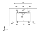
- the interval W1 in the predetermined direction between the at least two holes 43, 44, 45, 46, 83, 84, 85, 86 is the predetermined interval between the connection members 20, 60, 61, 62. It is larger than the width W2 in the direction.
- the case bodies 40, 80 have elastic locking portions 42, 82 for locking the display panels 10, 50, 51.
- the elastic locking portion 42 has a pressing piece 42b.
- the circuit board can be removed from the case body without damaging the display panel.
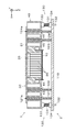
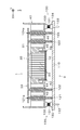
- Sectional drawing which shows embodiment which shows 1st embodiment of this invention Explanatory drawing of the state which set the liquid crystal display device which shows embodiment same as the above to the jig
- FIG. Explanatory drawing of the state which set the liquid crystal display device which shows embodiment same as the above to the jig
- FIG. Explanatory drawing of the state which set the liquid crystal display device which shows embodiment same as the above to the jig
- FIG. The front view which shows 3rd embodiment of this invention.
- the liquid crystal display device 1 includes a liquid crystal display panel 10, a connection member 20, a circuit board 30, and a case body 40.
- the liquid crystal display panel 10 is obtained by sticking polarizing plates to both front and rear surfaces of a liquid crystal cell in which liquid crystal is sealed in a pair of translucent substrates on which transparent electrodes are formed.
- the liquid crystal display panel 10 is held on the front side of the case body 40.
- the liquid crystal display panel 10 is driven by a driver circuit mounted on the circuit board 30 and displays an accumulated travel distance of the vehicle.
- the liquid crystal display panel 10 is transmitted and illuminated by a light emitting element such as an LED (Light Emitting Diode) mounted on the front surface of the circuit board 30.
- connection member 20 is composed of a plurality of metal terminals. One end of the connection member 20 is electrically connected to the liquid crystal display panel 10, and the other end of the connection member 20 is electrically connected to the circuit board 30 via the connector member 35. Connected to.
- the circuit board 30 is obtained by forming a wiring pattern made of copper foil on a base material 31 made of glass epoxy resin. A connector member 35 into which the other end of the connection member 20 is inserted is mounted on the circuit board 30.
- the circuit board 30 is formed with a through hole 32 into which protrusions 121a and 124a of pins 121 and 124 described later are inserted.
- the case body 40 is made of an opaque resin, and the liquid crystal display panel 10 is held on the front side of the case body 40.
- the circuit board 30 is held on the rear surface side of the case body 40 by an elastic locking portion (not shown).
- the case body 40 includes a support portion 41 that supports the liquid crystal display panel 10 and an elastic locking portion 42 that locks the liquid crystal display panel 10.
- the support portion 41 and the elastic locking portion 42 allow the liquid crystal display to be displayed.
- the panel 10 is held.
- the elastic locking portion 42 of the case body 40 includes a locking claw 42a that locks the liquid crystal display panel 10 and a pressing piece 42b that is pressed by pins 222 and 223 of the jig 3 described later.
- the elastic locking portion 42 of the case body 40 is elastically deformed when the pressing piece 42 b is pressed, and the locking claw 42 releases the liquid crystal display panel 10.
- the case body 40 is formed with holes 43, 44, 45, 46 through which pins described later are inserted.
- the holes 43, 44, 45, 46 of the case body 40 pass through the case body 40. Electric parts are not mounted at locations corresponding to the holes 43, 44, 45, 46 on the front surface of the circuit board 30.
- the jig 2 includes a base 110, pins 121, 122, 123, and 124, and a movable part 130.
- the base 110 of the jig 2 is made of metal or resin and has a flat plate shape.
- the pins 121, 122, 123, and 124 are made of metal or resin and have a substantially cylindrical shape.
- the pins 121, 122, 123, and 124 are provided vertically from the upper surface of the base 110.
- the upper end surfaces of the pins 122 and 123 are flat.
- projections 121 a and 124 a for positioning the circuit board 30 are formed on the upper end surfaces of the pins 121 and 124.
- the movable part 130 includes a coil spring 131, a rod part 132 inserted through the coil spring 131, a contact part 133 to which the upper end of the rod part 132 is fixed, and a base part 134 fixed to the base 110.
- the upper surface of the contact portion 133 is a flat surface and contacts the front surface of the case body 40.
- the rod part 132 of the movable part 130 has a cylindrical shape and penetrates the base part 134 and the base 110.
- the contact part 133 of the movable part 130 can move in the vertical direction within a predetermined stroke range.
- the jig 3 includes a base 210, pins 221, 222, 223, and 224, a movable portion 230, and a base 240.
- the base 210 of the jig 3 is made of metal or resin and has a flat plate shape.
- the movable part 230 includes a coil spring 231, a rod part 232 inserted through the coil spring 231, a contact part 233 to which the upper end of the rod part 232 is fixed, and a base part 234 fixed to the base 210.
- the upper surface of the contact portion 233 is a flat surface and contacts the front surface of the case body 40.
- the rod part 232 of the movable part 230 has a cylindrical shape and penetrates the base part 234 and the base 210.
- the contact part 233 of the movable part 230 can move in the vertical direction within a predetermined stroke range.
- the base 240 of the jig 3 includes a flat plate-shaped receiving portion 241, a cushion portion 242 attached to the upper surface of the receiving portion 241, and a support column 243 that supports the receiving portion 241.
- the receiving part 241 of the pedestal 240 has a rectangular shape larger than that of the liquid crystal display panel 10 and is disposed at a predetermined height from the upper surface of the base 210.
- the cushion portion 242 of the pedestal 240 is made of a buffer member such as silicone rubber.
- the liquid crystal display device 1 is turned over and the liquid crystal display device 1 is set on the jig 2 (see FIG. 2).
- the pins 121, 122, 123, 124 of the jig 2 are inserted into the holes 43, 44, 45, 46 of the case body 40, respectively, and the upper surfaces of the pins 121, 122, 123, 124 of the jig 2 are inserted. Abuts against the front surface of the circuit board 30.
- the protrusions 121a and 124a of the pins 121 and 124 are inserted into the through holes 32 of the circuit board 30, and the circuit board 30 is positioned.
- FIG. 4 shows a state in which the liquid crystal display device 1 with the circuit board 30 removed is set on the jig 3.
- the pins 222 and 223 of the jig 3 abut against the pressing piece 42 b of the elastic locking portion 42.
- the liquid crystal display panel 10 is detached from the case body 40 by pressing the case body 40 and applying a downward force.
- the liquid crystal display panel 10 removed from the case body 40 is received by the base 240 of the jig 3.
- the circuit board 30 is removed by the jig 2, and the liquid crystal display panel 10 is removed by the jig 3.
- the circuit board 30 and the liquid crystal display panel 10 may be removed.
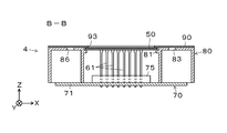
- the liquid crystal display device 4 includes a liquid crystal display panel 50, a connection member 60, a circuit board 70, a case body 80, and a display plate 90.
- the liquid crystal display panel 50 has polarizing plates attached to both front and rear surfaces of a liquid crystal cell in which liquid crystal is sealed in a pair of translucent substrates on which transparent electrodes are formed.
- the liquid crystal display panel 50 is held on the front side of the case body 80.
- the liquid crystal display panel 50 is driven by a driver circuit mounted on the circuit board 70 and displays the vehicle speed.
- the liquid crystal display panel 50 is transmitted and illuminated by a light emitting element 73 such as an LED (Light Emitting Diode) mounted on the front surface of the circuit board 70.
- Connection members 61 and 62 made up of a plurality of metal terminals are fixed to two opposite sides of the liquid crystal display panel 50.
- the connection members 61 and 62 electrically connect the liquid crystal display panel 50 and the circuit board 70.
- the connecting members 61 and 62 are arranged in the horizontal direction (X-axis direction) of the liquid crystal display panel 50 with a predetermined arrangement width W2.
- One end of the connection members 61 and 62 is electrically connected to the liquid crystal display panel 50, and the other end of the connection members 61 and 62 is inserted through the connector member 75.
- the circuit board 70 is obtained by forming a wiring pattern made of copper foil on a base material 71 made of glass epoxy resin.
- the circuit board 70 is locked to the rear surface of the case body 80 by an elastic locking piece (not shown).
- electrical components such as light emitting elements 72 and 73, a connector member 75, a driver circuit, and a capacitor are mounted.
- the case body 80 is made of an opaque resin, the liquid crystal display panel 50 is held on the front side of the case body 80, and the circuit board 70 is held on the rear side of the case body 80.
- the case body 80 includes a support portion 81 that supports the liquid crystal display panel 50 and an elastic locking portion 82 that locks the liquid crystal display panel 10.
- the support portion 81 and the elastic locking portion 82 provide liquid crystal display.
- the panel 50 is held.
- the case body 80 is formed with holes 83, 84, 85, 86 through which pins described later are inserted.
- the holes 83, 84, 85, 86 of the case body 80 pass through the case body 80. Electric parts are not mounted at locations corresponding to the holes 83, 84, 85, 86 on the front surface of the circuit board 70.
- the holes 83 and 84 of the case body 80 are arranged on the right side of the liquid crystal display panel 50 so as to have a predetermined interval W3 from the connection members 61 and 62.
- the holes 85 and 86 of the case body 80 are arranged on the left side of the liquid crystal display panel 50 so as to have a predetermined interval W4 from the connection members 61 and 62.
- the interval W1 between the hole portions 83 and 84 and the hole portions 85 and 86 is larger than the arrangement width W2 of the connection members 61 and 62.
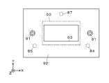
- the display plate 90 has a thin plate shape and includes a transmissive display portion 91 and a light shielding portion 92.
- the display board 90 is adhered to the front surface of the case body 80 with a double-sided adhesive member.
- the transmissive display portion 91 of the display board 90 is transmissively illuminated by the light emitting element 72 mounted on the circuit board 70.
- a rectangular window portion 93 for visually recognizing the display portion of the liquid crystal display panel 50 is formed on the display plate 90.
- the holes 83, 84, 85, 86 of the case body 80 are hidden by the light shielding portion 92 of the display plate 90 and are not visible from the front side of the liquid crystal display device 4.
- the jig 5 includes a base 310, pins 322 and 323, and a movable part 330.
- the base 310 of the jig 5 is made of metal or resin and has a flat plate shape.
- the pins 322 and 323 are made of metal or resin and have a substantially cylindrical shape.
- the pins 322 and 323 are provided vertically from the upper surface of the base 310.
- the display board 90 is not attached to the case body 80.
- the liquid crystal display device 4 is turned over, and the liquid crystal display device 4 is set on the jig 5.
- the pins 322 and 323 of the jig 5 are inserted into the holes 83, 84, 85 and 86 of the case body 80, respectively, and the upper surfaces of the pins 322 and 323 of the jig 5 abut against the front surface of the circuit board 70. Touch.
- the connection inserted through the connector member 75 of the circuit board 70 in the direction perpendicular to the liquid crystal display panel 50 (Z-axis direction) by pressing the case body 80 of the liquid crystal display device 4 and applying a downward force F.
- the members 61 and 62 are pulled out from the connector 75.
- the number of holes 83, 84, 85, 86 of the case body 80 be three or more and not on a straight line, and the connection member 61 while the circuit board 70 remains parallel to the liquid crystal display panel 50. , 62 can be pulled out from the connector 75. Further, since the interval W1 between the hole portions 83, 84 and the hole portions 85, 86 is larger than the arrangement width W2 of the connection members 61, 62, the liquid crystal display panel 50 is not subjected to excessive stress and connected. The members 61 and 62 can be pulled out from the connector 75.
- the circuit boards 30 and 70 in which the connection members 20, 61 and 62 are inserted into the connector members 35 and 75 are connected to the case body 40, 80 can be removed.
- the present invention is not limited to the first and second embodiments, and various modifications are possible.
- the display panel may be an organic EL panel.
- the number of holes 84, 85, 87 of the case body 80 may be three.
- the connection member 60 may be provided on one side of the liquid crystal display panel 50.
- the holes 83, 84, 85, 86 of the case body 80 are concealed by the light shielding portion 92 of the display plate 90.
- the non-transparent display portion is provided on the display plate.
- the hole portion may be hidden by the transmissive display portion.
- the present invention is suitable for a display device in which a liquid crystal display panel and a circuit board are housed in a case body.
- Liquid crystal display panel (display panel) DESCRIPTION OF SYMBOLS 20 Connection member 30 Circuit board 35 Connector member 40 Case body 42 Elastic locking part 42b Press piece 43 Hole part 44 Hole part 45 Hole part 46 Hole part 50 Liquid crystal display panel (display panel) 60 connecting member 61 connecting member 62 connecting member 70 circuit board 72 light emitting element 75 connector member 80 case body 82 elastic locking portion 83 hole portion 84 hole portion 85 hole portion 86 hole portion 87 hole portion 90 display plate 91 transmissive display portion (display) Part)
Landscapes
- Engineering & Computer Science (AREA)
- Chemical & Material Sciences (AREA)
- Combustion & Propulsion (AREA)
- Transportation (AREA)
- Mechanical Engineering (AREA)
- Devices For Indicating Variable Information By Combining Individual Elements (AREA)
- Instrument Panels (AREA)
- Liquid Crystal (AREA)
Abstract
表示パネルを損傷させることなく、ケース体から回路基板を外すことが可能な表示装置を提供する。 接続部材20は、表示パネル10に一端が電気的に接続される。回路基板30は、接続部材20の他端が電気的に接続される。ケース体40は、表示パネル10を保持する。ケース体40は、回路基板30を押圧するピンを挿通可能な孔部43,44,45,46を有する。ケース体40は、表示パネル20を係止する弾性係止部42を有する。弾性係止部42は、押圧片42bを有する。
Description
本発明は、液晶表示パネル等の表示パネルを備えた表示装置に関するものである。
従来より、液晶表示パネルを備えた車両用表示装置が種々提案されており、例えば特許文献1,特許文献2に開示されている。斯かる車両用表示装置は、積算走行距離等を表示する液晶表示パネルを備えており、この液晶表示パネルは金属製の金属端子によって回路基板と電気的に接続されている。
しかしながら、回路基板をケース体から外すときに、液晶表示パネルを損傷させる虞があった。例えば、車両用表示装置の製造工程において、回路基板に不良個所が発見された場合、ケース体から回路基板を外す必要がある。また、ケース体にキズが発見された場合、液晶表示パネル及び回路基板をケース体から外して、その外した液晶表示パネルを、再度、キズが無いケース体に組付ける必要があるが、回路基板をケース体から外すときに、液晶表示パネルを損傷させる虞があった。
本発明は、表示パネルを損傷させることなく、ケース体から回路基板を外すことが可能な表示装置を提供するものである。
本発明は、表示パネルを損傷させることなく、ケース体から回路基板を外すことが可能な表示装置を提供するものである。
本発明は、表示パネル10,50,51と、前記表示パネル10,50,51に一端が電気的に接続される接続部材20,60,61,62と、前記接続部材20,60,61,62の他端が電気的に接続される回路基板30,70と、前記表示パネル10,50,51を保持するケース体40,80と、を備えた表示装置1,4であって、前記ケース体40,80は、前記回路基板30,70を押圧するピン121,122,123,124,322,323を挿通可能な複数の孔部43,44,45,46,83,84,85,86,87を有するものである。
また、本発明は、表示パネル50,51と、前記表示パネル50,51に一端が電気的に接続される接続部材60,61,62と、前記接続部材60,61,62の他端が電気的に接続される回路基板70と、前記表示パネル50,51を保持するケース体80と、前記回路基板70に搭載された発光素子72と、前記発光素子72によって透過照明される表示部91を有する表示板90と、を備えた表示装置であって、前記ケース体80は前記回路基板70を押圧するピン322,323を挿通可能な複数の孔部83,84,85,86,87を有すると共に、前記孔部83,84,85,86,87は前記表示板90の前記表示部91がない個所で隠されるものである。
また、本発明は、前記ケース体40,80は、少なくとも3個の前記孔部43,44,45,46,83,84,85,86,87を有するものである。
前記接続部材20,60,61,62の前記他端は、前記回路基板30,70に搭載されたコネクタ部材35,75に挿通されているものである。
また、本発明は、前記接続部材20,60,61,62は、所定方向に配列された複数の金属端子からなるものである。
また、本発明は、少なくとも2個の前記孔部43,44,45,46,83,84,85,86の前記所定方向の間隔W1は、前記接続部材20,60,61,62の前記所定方向の幅W2よりも大きいものである。
また、本発明は、前記ケース体40,80は、前記表示パネル10,50,51を係止する弾性係止部42,82を有するものである。
また、本発明は、前記弾性係止部42は、押圧片42bを有するものである。
表示パネルを損傷させることなく、ケース体から回路基板を外すことができる。
以下、添付図面に基づいて、本発明の一実施形態を説明する。図1乃至図4は、第一実施形態を示すものである。液晶表示装置1は、液晶表示パネル10と、接続部材20と、回路基板30と、ケース体40とを備えている。
液晶表示パネル10は、透明電極が形成された一対の透光性基板に液晶を封入した液晶セルの前後両面に偏光板を貼着したものである。液晶表示パネル10は、ケース体40の前面側に保持されている。液晶表示パネル10は、回路基板30に搭載されたドライバー回路によって駆動され、車両の積算走行距離を表示する。また、液晶表示パネル10は、回路基板30の前面に搭載されたLED(Light Emitting Diode)等の発光素子によって透過照明される。
接続部材20は複数の金属端子からなるものであり、接続部材20の一端が液晶表示パネル10に電気的に接続され、接続部材20の他端がコネクタ部材35を介して回路基板30に電気的に接続される。回路基板30は、ガラスエポキシ樹脂からなる基材31に、銅箔からなる配線パターンを形成したものである。回路基板30には、接続部材20の他端が挿通されるコネクタ部材35が搭載されている。回路基板30には、後述するピン121,124の突起121a,124aが挿入される貫通孔32が形成されている。
ケース体40は不透明な樹脂からなるものであり、ケース体40の前面側に液晶表示パネル10が保持されている。回路基板30は、弾性係止部(図示しない)によって、ケース体40の後面側に保持されている。ケース体40は、液晶表示パネル10を支持する支持部41と、液晶表示パネル10を係止する弾性係止部42とを有しており、支持部41及び弾性係止部42により、液晶表示パネル10を保持している。
ケース体40の弾性係止部42は、液晶表示パネル10を係止する係止爪42aと、後述する治具3のピン222,223に押圧される押圧片42bとを有している。ケース体40の弾性係止部42は、押圧片42bを押圧したときに弾性変形し、係止爪42が液晶表示パネル10を解放するようになっている。ケース体40には、後述するピンが挿通される孔部43,44,45,46が形成されている。ケース体40の孔部43,44,45,46は、ケース体40を貫通するものである。回路基板30の前面の、孔部43,44,45,46に対応する個所には、電気部品が搭載されていない。
治具2は、基台110と、ピン121,122,123,124と、可動部130とを備えている。
治具2の基台110は、金属または樹脂からなるものであり、平板形状になっている。ピン121,122,123,124は、金属または樹脂からなるものであり、略円柱形状になっている。ピン121,122,123,124は、基台110の上面から垂直に設けられている。ピン122,123の上端面は、平面になっている。一方、ピン121,124の上端面には、回路基板30を位置決めする突起121a,124aが形成されている。
可動部130は、コイルバネ131と、このコイルバネ131に挿通されるロッド部132と、このロッド部132の上端が固定される当接部133と、基台110に固定されたベース部134と、を有している。当接部133の上面は、平面になっており、ケース体40の前面に当接する。可動部130のロッド部132は、円柱形状になっており、ベース部134及び基台110を貫通している。可動部130の当接部133は、所定のストローク範囲で、上下方向に移動することができる。
治具3は、基台210と、ピン221,222,223,224と、可動部230と、台座240とを備えている。治具3の基台210は、金属または樹脂からなるものであり、平板形状になっている。
可動部230は、コイルバネ231と、このコイルバネ231に挿通されるロッド部232と、このロッド部232の上端が固定される当接部233と、基台210に固定されたベース部234と、を有している。当接部233の上面は、平面になっており、ケース体40の前面に当接する。可動部230のロッド部232は、円柱形状になっており、ベース部234及び基台210を貫通している。可動部230の当接部233は、所定のストローク範囲で、上下方向に移動することができる。
治具3の台座240は、平板形状の受け部241と、この受け部241の上面に貼着されたクッション部242と、受け部241を支持する支柱243とを有している。台座240の受け部241は、液晶表示パネル10よりも大きな矩形状になっており、基台210の上面から所定高さに配置されている。台座240のクッション部242は、シリコーンゴム等の緩衝部材からなるものである。
次に、図2及び図3に基づいて、接続部材20がコネクタ部材35に挿通された回路基板30をケース体40から外す方法について説明する。
先ず、液晶表示装置1を裏返して、治具2に液晶表示装置1をセットする(図2参照)。このとき、治具2のピン121,122,123,124は、夫々、ケース体40の孔部43,44,45,46に挿通され、治具2のピン121,122,123,124の上面が回路基板30の前面に当接する。ピン121,124の突起121a,124aは、回路基板30の貫通孔32に挿入され、回路基板30が位置決めされる。
次に、液晶表示装置1のケース体40を押して、下向きの力Fを加えることにより、コネクタ部材35から接続部材20が抜けて、回路基板30がケース体40から外れる(図3参照)。
図4は、回路基板30が外された液晶表示装置1を治具3にセットした状態を示すものである。
回路基板30が外された液晶表示装置1を治具3にセットしたとき、治具3のピン222,223は、弾性係止部42の押圧片42bに当接する。次に、ケース体40を押して、下向きの力を加えることにより、液晶表示パネル10が、ケース体40から外れる。そして、ケース体40から外れた液晶表示パネル10は、治具3の台座240で受け止められる。
第一実施形態は、治具2により回路基板30を外し、治具3により液晶表示パネル10を外すものであったが、治具2と治具3との作用を組み合わせた1個の治具により、回路基板30及び液晶表示パネル10を外せるように構成しても良い。
図5乃至図9は、第二実施形態を示すものである。液晶表示装置4は、液晶表示パネル50と、接続部材60と、回路基板70と、ケース体80と、表示板90とを備えている。
液晶表示パネル50は、透明電極が形成された一対の透光性基板に液晶を封入した液晶セルの前後両面に偏光板を貼着したものである。液晶表示パネル50は、ケース体80の前面側に保持されている。液晶表示パネル50は、回路基板70に搭載されたドライバー回路によって駆動され、車両速度を表示する。また、液晶表示パネル50は、回路基板70の前面に搭載されたLED(Light Emitting Diode)等の発光素子73によって透過照明される。
液晶表示パネル50の対向する2辺には、複数の金属端子からなる接続部材61,62が固定されている。接続部材61,62は、液晶表示パネル50と回路基板70とを電気的に接続する。接続部材61,62は、液晶表示パネル50の横方向(X軸方向)に、所定の配列幅W2で配列されている。接続部材61,62の一端は液晶表示パネル50に電気的に接続され、接続部材61,62の他端はコネクタ部材75に挿通されている。
回路基板70は、ガラスエポキシ樹脂からなる基材71に、銅箔からなる配線パターンを形成したものである。回路基板70は、ケース体80の後面に、弾性係止片(図示しない)で係止されている。回路基板70には、発光素子72,73,コネクタ部材75,ドライバー回路,コンデンサ等の電気部品が実装されている。
ケース体80は不透明な樹脂からなるものであり、ケース体80の前面側に液晶表示パネル50が保持され、ケース体80の後面側に回路基板70が保持される。ケース体80は、液晶表示パネル50を支持する支持部81と、液晶表示パネル10を係止する弾性係止部82とを有しており、支持部81及び弾性係止部82により、液晶表示パネル50を保持している。
ケース体80には、後述するピンが挿通される孔部83,84,85,86が形成されている。ケース体80の孔部83,84,85,86は、ケース体80を貫通するものである。回路基板70の前面の、孔部83,84,85,86に対応する個所には、電気部品が搭載されていない。
ケース体80の孔部83,84は、接続部材61,62から所定間隔W3を有するように、液晶表示パネル50の右側に配置されている。ケース体80の孔部85,86は、接続部材61,62から所定間隔W4を有するように、液晶表示パネル50の左側に配置されている。孔部83,84と孔部85,86との間隔W1は、接続部材61,62の配列幅W2よりも大きくなっている。
表示板90は、薄板形状になっており、透過表示部91及び遮光部92を有している。表示板90は、両面粘着部材にてケース体80の前面に貼着されている。表示板90の透過表示部91は、回路基板70に搭載された発光素子72によって透過照明される。表示板90には、液晶表示パネル50の表示部を視認するための矩形の窓部93が形成されている。ケース体80の孔部83,84,85,86は、表示板90の遮光部92によって隠され、液晶表示装置4の前面側からは視認されない。
治具5は、基台310と、ピン322,323と、可動部330とを備えている。治具5の基台310は、金属または樹脂からなるものであり、平板形状になっている。ピン322,323は、金属または樹脂からなるものであり、略円柱形状になっている。ピン322,323は、基台310の上面から垂直に設けられている。
次に、図9に基づいて、接続部材60がコネクタ部材75に挿通された回路基板70をケース体80から外す方法について説明する。なお、この場合、表示板90はケース体80に貼着されていない。
先ず、液晶表示装置4を裏返して、治具5に液晶表示装置4をセットする。このとき、治具5のピン322,323は、夫々、ケース体80の孔部83,84,85,86に挿通され、治具5のピン322,323の上面が回路基板70の前面に当接する。次に、液晶表示装置4のケース体80を押して、下向きの力Fを加えることにより、液晶表示パネル50と垂直な方向(Z軸方向)に、回路基板70のコネクタ部材75に挿通された接続部材61,62がコネクタ75から引き抜かれる。
ケース体80の孔部83,84,85,86は、3個以上で、且つ、1直線上にないことが望ましく、回路基板70が液晶表示パネル50と平行な状態のままで、接続部材61,62をコネクタ75から引き抜くことができる。また、孔部83,84と孔部85,86との間隔W1は、接続部材61,62の配列幅W2よりも大きくなっているため、液晶表示パネル50に過度の応力が加わることなく、接続部材61,62をコネクタ75から引き抜くことができる。
第一,第二実施形態によれば、液晶表示パネル10,50を損傷させることなく、コネクタ部材35,75に接続部材20,61,62が挿通された回路基板30,70をケース体40,80から外すことができる。
なお、本発明は、第一,第二実施形態に限定されるものではなく、種々の変形が可能であり、例えば、表示パネルは、有機ELパネルであっても良い。また、図10及び図11に示す第三実施形態のように、ケース体80の孔部84,85,87は3個であっても良い。また、接続部材60は、液晶表示パネル50の一辺に設けても良い。
また、第二実施形態は、ケース体80の孔部83,84,85,86が、表示板90の遮光部92によって隠されるものであるが、表示板に不透過表示部を設け、この不透過表示部によって孔部を隠しても良い。
本発明は、液晶表示パネルと回路基板とをケース体に収納した表示装置に好適である。
10 液晶表示パネル(表示パネル)
20 接続部材
30 回路基板
35 コネクタ部材
40 ケース体
42 弾性係止部
42b 押圧片
43 孔部
44 孔部
45 孔部
46 孔部
50 液晶表示パネル(表示パネル)
60 接続部材
61 接続部材
62 接続部材
70 回路基板
72 発光素子
75 コネクタ部材
80 ケース体
82 弾性係止部
83 孔部
84 孔部
85 孔部
86 孔部
87 孔部
90 表示板
91 透過表示部(表示部)
20 接続部材
30 回路基板
35 コネクタ部材
40 ケース体
42 弾性係止部
42b 押圧片
43 孔部
44 孔部
45 孔部
46 孔部
50 液晶表示パネル(表示パネル)
60 接続部材
61 接続部材
62 接続部材
70 回路基板
72 発光素子
75 コネクタ部材
80 ケース体
82 弾性係止部
83 孔部
84 孔部
85 孔部
86 孔部
87 孔部
90 表示板
91 透過表示部(表示部)
Claims (8)
- 表示パネルと、前記表示パネルに一端が電気的に接続される接続部材と、前記接続部材の他端が電気的に接続される回路基板と、前記表示パネルを保持するケース体と、を備えた表示装置であって、
前記ケース体は、前記回路基板を押圧するピンを挿通可能な複数の孔部を有することを特徴とする表示装置。 - 表示パネルと、前記表示パネルに一端が電気的に接続される接続部材と、前記接続部材の他端が電気的に接続される回路基板と、前記表示パネルを保持するケース体と、前記回路基板に搭載された発光素子と、前記発光素子によって透過照明される表示部を有する表示板と、を備えた表示装置であって、
前記ケース体は前記回路基板を押圧するピンを挿通可能な複数の孔部を有すると共に、前記孔部は前記表示板の前記表示部がない個所で隠されることを特徴とする表示装置。 - 前記ケース体は、少なくとも3個の前記孔部を有することを特徴とする請求項1または請求項2に記載の表示装置。
- 前記接続部材の前記他端は、前記回路基板に搭載されたコネクタ部材に挿通されていることを特徴とする請求項1または請求項2に記載の表示装置。
- 前記接続部材は、所定方向に配列された複数の金属端子からなることを特徴とする請求項1または請求項2に記載の表示装置。
- 少なくとも2個の前記孔部の前記所定方向の間隔は、前記接続部材の前記所定方向の幅よりも大きいことを特徴とする請求項5に記載の表示装置。
- 前記ケース体は、前記表示パネルを係止する弾性係止部を有することを特徴とする請求項1に記載の表示装置。
- 前記弾性係止部は、押圧片を有することを特徴とする請求項7に記載の表示装置。
Priority Applications (1)
| Application Number | Priority Date | Filing Date | Title |
|---|---|---|---|
| CN201480026574.4A CN105209862A (zh) | 2013-05-13 | 2014-05-12 | 显示装置 |
Applications Claiming Priority (2)
| Application Number | Priority Date | Filing Date | Title |
|---|---|---|---|
| JP2013101547A JP6044448B2 (ja) | 2013-05-13 | 2013-05-13 | 表示装置 |
| JP2013-101547 | 2013-05-13 |
Publications (1)
| Publication Number | Publication Date |
|---|---|
| WO2014185382A1 true WO2014185382A1 (ja) | 2014-11-20 |
Family
ID=51898360
Family Applications (1)
| Application Number | Title | Priority Date | Filing Date |
|---|---|---|---|
| PCT/JP2014/062612 Ceased WO2014185382A1 (ja) | 2013-05-13 | 2014-05-12 | 表示装置 |
Country Status (3)
| Country | Link |
|---|---|
| JP (1) | JP6044448B2 (ja) |
| CN (1) | CN105209862A (ja) |
| WO (1) | WO2014185382A1 (ja) |
Families Citing this family (1)
| Publication number | Priority date | Publication date | Assignee | Title |
|---|---|---|---|---|
| JP6569904B2 (ja) * | 2015-11-17 | 2019-09-04 | 日本精機株式会社 | 車両用表示装置 |
Citations (2)
| Publication number | Priority date | Publication date | Assignee | Title |
|---|---|---|---|---|
| JP2005010063A (ja) * | 2003-06-20 | 2005-01-13 | Calsonic Kansei Corp | 車両用メータの照明構造 |
| WO2011077997A1 (ja) * | 2009-12-25 | 2011-06-30 | 日本精機株式会社 | 表示装置 |
Family Cites Families (5)
| Publication number | Priority date | Publication date | Assignee | Title |
|---|---|---|---|---|
| JP4046011B2 (ja) * | 2003-05-29 | 2008-02-13 | 松下電器産業株式会社 | 平板型画像表示装置 |
| KR101100169B1 (ko) * | 2004-11-10 | 2011-12-28 | 엘지전자 주식회사 | 가전기기의 원격 모니터 장치 |
| JP4729560B2 (ja) * | 2005-03-08 | 2011-07-20 | 日本写真印刷株式会社 | タッチパネルユニット |
| DE202007005013U1 (de) * | 2007-04-03 | 2008-08-07 | Weidmüller Interface GmbH & Co. KG | Leiterplattenverbinder |
| JP5605243B2 (ja) * | 2011-01-31 | 2014-10-15 | 日本精機株式会社 | 表示装置 |
-
2013
- 2013-05-13 JP JP2013101547A patent/JP6044448B2/ja not_active Expired - Fee Related
-
2014
- 2014-05-12 WO PCT/JP2014/062612 patent/WO2014185382A1/ja not_active Ceased
- 2014-05-12 CN CN201480026574.4A patent/CN105209862A/zh active Pending
Patent Citations (2)
| Publication number | Priority date | Publication date | Assignee | Title |
|---|---|---|---|---|
| JP2005010063A (ja) * | 2003-06-20 | 2005-01-13 | Calsonic Kansei Corp | 車両用メータの照明構造 |
| WO2011077997A1 (ja) * | 2009-12-25 | 2011-06-30 | 日本精機株式会社 | 表示装置 |
Also Published As
| Publication number | Publication date |
|---|---|
| CN105209862A (zh) | 2015-12-30 |
| JP2014222180A (ja) | 2014-11-27 |
| JP6044448B2 (ja) | 2016-12-14 |
Similar Documents
| Publication | Publication Date | Title |
|---|---|---|
| CN104137167B (zh) | 显示装置 | |
| US8414307B2 (en) | Connection structure having a printed circuit board with a protrusion engaging a receiving portion of a second circuit board | |
| CN101667373B (zh) | 显示装置 | |
| CN102998821A (zh) | 显示装置及其弹性外框 | |
| US8941608B2 (en) | Liquid crystal display with detachable touch sensor | |
| MX2011012349A (es) | Dispositivo de fuentes de luz y dispositivo de presentacion visual. | |
| CN103438408A (zh) | 一种led灯条连接器及背光模组 | |
| TW200951538A (en) | Flexible display module and method of manufacturing the same | |
| CN103335253B (zh) | 背光模组及包含其的液晶显示器 | |
| KR101009280B1 (ko) | 인쇄회로기판의 갭 서포터 및 그 제조방법 | |
| CN209674745U (zh) | 显示装置 | |
| CN102379021A (zh) | 电容型输入开关 | |
| KR20150002046A (ko) | 회로기판 및 상기 회로기판을 포함하는 조명장치 | |
| US10739886B2 (en) | Touch panel and touch display device | |
| WO2010121666A3 (en) | Electronic structure | |
| JP6044448B2 (ja) | 表示装置 | |
| KR101621062B1 (ko) | 필름형 프로브 유닛 | |
| JP6048061B2 (ja) | 液晶表示装置 | |
| JP2012160505A (ja) | 表示装置 | |
| KR101165158B1 (ko) | 기판 갭 서포터 및 그 제조방법 | |
| TW200720753A (en) | Anisotropic conductive film and flat panel display using the same, and method for manufacturing the same | |
| CN103329031A (zh) | 液晶显示装置 | |
| JP6543020B2 (ja) | 電気回路端子装置 | |
| JP2012225648A (ja) | コンタクトブロック | |
| JP2015052732A (ja) | 表示装置 |
Legal Events
| Date | Code | Title | Description |
|---|---|---|---|
| 121 | Ep: the epo has been informed by wipo that ep was designated in this application |
Ref document number: 14797171 Country of ref document: EP Kind code of ref document: A1 |
|
| NENP | Non-entry into the national phase |
Ref country code: DE |
|
| 122 | Ep: pct application non-entry in european phase |
Ref document number: 14797171 Country of ref document: EP Kind code of ref document: A1 |