WO2014175299A1 - スイッチング電源装置用制御回路 - Google Patents
スイッチング電源装置用制御回路 Download PDFInfo
- Publication number
- WO2014175299A1 WO2014175299A1 PCT/JP2014/061358 JP2014061358W WO2014175299A1 WO 2014175299 A1 WO2014175299 A1 WO 2014175299A1 JP 2014061358 W JP2014061358 W JP 2014061358W WO 2014175299 A1 WO2014175299 A1 WO 2014175299A1
- Authority
- WO
- WIPO (PCT)
- Prior art keywords
- transistor
- circuit
- control signal
- power supply
- external control
- Prior art date
- Legal status (The legal status is an assumption and is not a legal conclusion. Google has not performed a legal analysis and makes no representation as to the accuracy of the status listed.)
- Ceased
Links
Images




Classifications
-
- H—ELECTRICITY
- H03—ELECTRONIC CIRCUITRY
- H03K—PULSE TECHNIQUE
- H03K17/00—Electronic switching or gating, i.e. not by contact-making and –breaking
- H03K17/04—Modifications for accelerating switching
- H03K17/042—Modifications for accelerating switching by feedback from the output circuit to the control circuit
- H03K17/04213—Modifications for accelerating switching by feedback from the output circuit to the control circuit in bipolar transistor switches
-
- H—ELECTRICITY
- H03—ELECTRONIC CIRCUITRY
- H03K—PULSE TECHNIQUE
- H03K17/00—Electronic switching or gating, i.e. not by contact-making and –breaking
- H03K17/06—Modifications for ensuring a fully conducting state
Definitions
- the present invention relates to a control circuit for a switching power supply device that switches operation start or stop in response to an external trigger signal.
- Patent Document 1 is configured to input an STB signal (standby signal) from the outside. That is, a circuit is provided that clamps the PWM signal for the drive circuit of the switching element to a predetermined level when the STB signal is asserted and validates the PWM signal when the STB signal becomes negated.
- the terminal for inputting the STB signal is a terminal used to control the start / stop of the operation of the switching power supply device from the outside, so it is also referred to as a remote terminal, and the signal input thereto is also referred to as a remote signal.
- the signal input to the remote terminal of the switching control circuit is a binary logic level signal. Therefore, when the level of the control signal used as the remote signal can take an intermediate potential between the high level and the low level, or when the control signal is a signal output from a circuit having a different voltage level. Is provided with a waveform shaping circuit (binarization circuit) for binarizing the control signal.
- the switching control circuit repeats driving start / stop of the switching circuit within a short time, and the operation becomes unstable.
- an object of the present invention is to generate a stable remote signal even when the change of an externally generated control signal is extremely slow or the voltage transition is unstable. It is an object of the present invention to provide a switching power supply control circuit capable of performing stable switching control.
- a control circuit for a switching power supply device includes a switching control circuit that receives an external control signal and starts / stops driving of a switching element, and is connected between a transistor and a collector of the transistor and a power supply
- a plurality of transistor circuits having an emitter grounded, a base as an input section, and a collector as an output section, an output section of an even-numbered transistor circuit, and an input section of a first-stage transistor circuit;
- a positive feedback resistor is connected between them, an external control signal is input to the first stage, and a control signal is output from the transistor circuit of the final stage.
- the transistors of the first-stage transistor circuit are By turning on the external control signal, the even-numbered transistors are turned off. This off-state is positively fed back to the first-stage transistor circuit, and the first-stage transistor is reliably turned on, and that state is maintained. That is, the voltage applied to the base of the first transistor element is a composite value of the collector voltage of the even-numbered transistor element and the voltage of the external control signal. Therefore, even if the voltage change of the external control signal input to the first stage transistor circuit is extremely slow or the voltage transition is unstable, a stable remote signal is generated.
- the number of stages of the transistor circuit is preferably an odd number. Thereby, the voltage level of the input control signal and the voltage level of the remote signal can be inverted, and it is possible to easily cope with the case where the logic is to be inverted.
- the number of stages of the transistor circuit is preferably an even number. Thereby, the logical relationship between the voltage level of the input control signal and the voltage level of the remote signal can be maintained.
- a resistor is connected in series between the input portion of the first stage transistor circuit and the input portion of the external control signal.
- a stable remote signal is generated even if the voltage change of the external control signal input to the first stage transistor circuit is extremely slow or the voltage transition is unstable.
- FIG. 1 is a circuit diagram of a switching power supply device according to the first embodiment.
- FIG. 2 is a diagram referred to in the description of the quantitative operation of the positive feedback with respect to the base of the transistor Q1 in the first stage of the remote signal generation circuit.
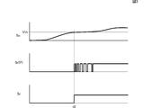
- FIG. 3 is a diagram showing the difference in the remote signal depending on the presence or absence of the positive feedback resistor, and is a waveform diagram schematically showing the voltage change of the remote signal Sr with respect to the voltage change of the external control signal Sc.
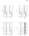
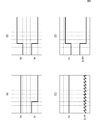
- 4A and 4B are waveform diagrams of the remote signal generation circuit according to the first embodiment shown in FIG. 1, and FIGS. 4C and 4D are obtained by removing the positive feedback resistor Rf from FIG.
- FIG. 6 is a circuit diagram of a switching power supply device according to the second embodiment.
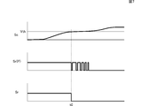
- FIG. 7 is a diagram showing the difference in the remote signal depending on the presence or absence of the positive feedback resistor, and is a waveform diagram schematically showing the voltage change of the remote signal Sr with respect to the voltage change of the external control signal Sc.
- 8A and 8B are waveform diagrams of the remote signal generation circuit according to the second embodiment shown in FIG. 6, and FIGS. 8C and 8D are obtained by removing the positive feedback resistor Rf from FIG. It is a wave form diagram of the remote signal generation circuit which concerns on a comparative example, and all are the wave form diagrams at the time of the rising of the external control signal Sc.
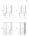
- 9A and 9B are waveform diagrams of the remote signal generation circuit according to the second embodiment shown in FIG. 6, and FIGS. 9C and 9D are obtained by removing the positive feedback resistor Rf from FIG. It is a wave form diagram of the remote signal generation circuit which concerns on a comparative example, and all are the wave form diagrams at the time of the fall of the external control signal Sc.
- FIG. 1 is a circuit diagram of a switching power supply device according to the first embodiment.
- This switching power supply device is a switching power supply device that converts the power supply voltage input to the power supply input terminal Vin and outputs it to the power supply output terminal Vout, and includes a switching circuit 20, a rectifying / smoothing circuit 30, and a switching control IC 10.
- the switching circuit 20 includes a switching element, and the switching control IC 10 starts / stops driving of the switching element.
- the switching power supply device includes a remote signal generation circuit 11 that inputs a control signal from the outside and gives a remote signal to the switching control IC 10.
- the switching control IC 10 and the remote signal generation circuit 11 constitute a “switching power supply control circuit” according to the present invention.
- the remote signal generation circuit 11 inputs the external control signal Sc to the input terminal Pc, and outputs the remote signal Sr from the output terminal Pr.
- the remote signal generation circuit 11 includes a two-stage transistor circuit.
- the one-stage transistor circuit includes a transistor whose emitter is grounded, and a load resistor connected between the collector of the transistor and a power supply, and uses the base of the transistor as an input section and the collector as an output section. That is, the first-stage transistor circuit is configured by the transistor Q1 and the load resistor Rc1, and the second-stage transistor circuit is configured by the transistor Q2 and the load resistor Rc2.
- a positive feedback resistor Rf is connected between the collector of the transistor Q2 which is the output part of the second-stage transistor circuit and the base of the transistor Q1 which is the input part of the first-stage transistor circuit. Further, a resistor Ri is connected in series between the base of the transistor Q1, which is the input part of the first stage transistor circuit, and the external control signal input terminal Pc.
- the operation of the remote signal generation circuit 11 shown in FIG. 1 is as follows.
- the transistor Q1 When the external control signal input to the external control signal input terminal Pc is at a low level (ground potential), the transistor Q1 is off, so that the collector potential of the transistor Q1 is almost the power supply potential. Since the collector potential of the transistor Q1 is the base potential of the transistor Q2, in this state, the transistor Q2 is on, and the remote signal output to the remote signal output terminal is at a low level (ground potential). When the transistor Q2 is turned on, the base potential of the transistor Q1 is further pulled to the ground potential via the positive feedback resistor Rf. That is, once the transistor Q1 is turned on triggered by the turn-off of the transistor Q1, the off state of the transistor Q1 is stabilized.
- the transistor Q1 when the external control signal is at a high level (power supply potential), the transistor Q1 is on, so that the collector potential of the transistor Q1 is almost the ground potential. Therefore, the transistor Q2 is in an off state, and the remote signal output to the remote signal output terminal is at a high level (power supply potential).
- the transistor Q2 When the transistor Q2 is turned off, the base potential of the transistor Q1 is further pulled to the power supply potential via the positive feedback resistor Rf. That is, once the transistor Q1 is turned off triggered by the turn-on of the transistor Q1, the on-state of the transistor Q1 is stabilized.
- the voltage of the external control signal input to the external control signal input terminal Pc is Vc
- the power supply voltage is Vcc
- the resistance value of the positive feedback resistor Rf is Rf
- the resistance value of the resistor Ri is Ri
- positive feedback When the voltage input to the resistor Rf (the collector voltage of the transistor Q2 in FIG. 1) is represented by Vf and the base voltage of the transistor Q1 is represented by Vb1, these are represented by the following relational expression.
- Vb1 Vc when there is no positive feedback resistor Rf, the base voltage of Q1 is multiplied by a coefficient of Rf / (Ri + Rf) with respect to the external control voltage Vc.
- the external control voltage Vc required for turning on the transistor Q1 is higher than the external control voltage Vc required for turning on the transistor Q1 when the positive feedback resistor Rf is present.
- Vf Vcc
- the external control voltage Vc required for turning off the transistor Q1 is lower than the external control voltage Vc required for turning off the transistor Q1 when the positive feedback resistor Rf is present.
- the noise margin when the first-stage transistor Q1 is turned on is widened when the second-stage transistor Q2 is on, and the first-stage transistor Q1 is turned off when the second-stage transistor Q2 is off.
- the noise margin becomes wider.
- an external trigger signal when the external control signal becomes the ground potential level (low level) can be obtained. Even if the output impedance of the generated circuit is low, it is possible to secure a current flowing through the transistor base of the first stage transistor circuit via the positive feedback resistor. That is, the positive feedback operation is reliably performed. However, if the output impedance of the circuit that generates the external control signal is high, that is, if there is a resistance corresponding to the resistance Ri in the circuit that generates the external control signal, the remote signal generation circuit 11 does not need the resistance Ri. is there.
- FIG. 3 is a diagram showing the difference in the remote signal depending on the presence or absence of the positive feedback resistor, and is a waveform diagram schematically showing the voltage change of the remote signals Sr, Sr (P) with respect to the voltage change of the external control signal Sc.
- the signal Sr is a remote signal when there is a positive feedback resistor
- the signal Sr (P) is a remote signal when there is no positive feedback resistor.
- the voltage of the external control signal Sc rises slowly, and when the voltage exceeds the threshold value Vth of the base-emitter voltage of the transistor Q1 at time t0, the remote signal Sr is inverted to high level. Since there is a state where the voltage of the external control signal slightly fluctuates around the threshold value Vth after t0, if there is no positive feedback resistance, as shown by the remote signal Sr (P) in FIG. And the state where the fluctuation of the low level repeats arises.
- FIGS. 4A and 4B are waveform diagrams of the remote signal generation circuit according to the first embodiment shown in FIG. 1, and FIGS. 4C and 4D show the positive feedback resistor Rf from FIG. It is a wave form diagram of the remote signal generation circuit concerning the comparative example removed.
- 4A and 4C are waveform diagrams when the external control signal Sc rises slowly
- FIGS. 4B and 4D are waveform diagrams when the external control signal Sc rises steeply.
- Each is a waveform diagram by actual measurement, the horizontal axis is 4 ⁇ s / div, the vertical axis is 2 V / div for the external control signal Sc, and 0.5 V / div for the remote signals Sr and Sr (P).
- both the remote signals Sr and Sr (P) rise steeply.
- the remote signal Sr has an oscillation waveform.
- the remote signal Sr that rises sharply can be obtained.
- FIGS. 5A and 5B are waveform diagrams of the remote signal generation circuit according to the first embodiment shown in FIG. 1, and FIGS. 5C and 5D show the positive feedback resistor Rf from FIG. It is a wave form diagram of the remote signal generation circuit concerning the comparative example removed.
- 5A and 5C are waveform diagrams when the external control signal Sc falls slowly
- FIGS. 5B and 5D are waveform diagrams when the external control signal Sc falls steeply. is there.
- the vertical and horizontal scales are the same as those shown in FIGS.
- Second Embodiment a switching power supply control circuit including a remote signal generation circuit having three transistors is shown.
- FIG. 6 is a circuit diagram of the switching power supply device according to the second embodiment.
- the switching power supply device includes a switching circuit 20, a rectifying / smoothing circuit 30, a switching control IC 10, and a remote signal generation circuit 11.
- the remote signal generation circuit 11 inputs the external control signal Sc to the input terminal Pc, and outputs the remote signal Sr from the output terminal Pr.
- the remote signal generation circuit 11 includes a three-stage transistor circuit.
- the transistor Q1 and the load resistor Rc1 constitute a first stage transistor circuit.
- the transistor Q2 and the load resistor Rc2 form a second stage transistor circuit
- the transistor Q3 and the load resistor Rc3 form a third stage transistor circuit.
- a positive feedback resistor Rf is connected between the collector of the transistor Q2 which is the output part of the second-stage transistor circuit and the base of the transistor Q1 which is the input part of the first-stage transistor circuit.
- a resistor Ri is connected in series between the base of the transistor Q1, which is the input section of the first stage transistor circuit, and the external control signal input terminal Pc.
- the remote signal is output from the collector of the third-stage transistor Q3.
- the operation of the remote signal generation circuit 11 shown in FIG. 6 is as follows.
- the transistor Q1 When the external control signal input to the external control signal input terminal Pc is at a low level (ground potential), the transistor Q1 is off, so that the collector potential of the transistor Q1 is almost the power supply potential. Since the collector potential of the transistor Q1 is the base potential of the transistor Q2, the transistor Q2 is in the on state and the transistor Q3 is in the off state in this state, and the remote signal output to the remote signal output terminal is high level (power supply potential). Become. When the transistor Q2 is turned on, the base potential of the transistor Q1 is further pulled to the ground potential via the positive feedback resistor Rf. That is, once the transistor Q1 is turned on triggered by the turn-off of the transistor Q1, the off state of the transistor Q1 is stabilized.
- the transistor Q1 when the external control signal is at a high level (power supply potential), the transistor Q1 is on, so that the collector potential of the transistor Q1 is almost the ground potential. Therefore, the transistor Q2 is in the off state, the transistor Q3 is in the on state, and the remote signal output to the remote signal output terminal is at a low level (ground potential).
- the transistor Q2 is turned off, the base potential of the transistor Q1 is further pulled to the power supply potential via the positive feedback resistor Rf. That is, once the transistor Q1 is turned off triggered by the turn-on of the transistor Q1, the on-state of the transistor Q1 is stabilized.
- the voltage level of the input control signal and the voltage level of the remote signal can be inverted, and this can be easily handled when it is desired to invert the logic.
- FIG. 7 is a diagram showing the difference in the remote signal depending on the presence or absence of the positive feedback resistor, and is a waveform diagram schematically showing the voltage change of the remote signals Sr, Sr (P) with respect to the voltage change of the external control signal Sc.
- the signal Sr is a remote signal when there is a positive feedback resistor
- the signal Sr (P) is a remote signal when there is no positive feedback resistor.
- the voltage of the external control signal Sc rises slowly, and when the voltage exceeds the threshold value Vth of the base-emitter voltage of the transistor Q1 at time t0, the remote signal Sr is inverted to a low level. Since there is a state where the voltage of the external control signal slightly fluctuates in the vicinity of the threshold value Vth after t0, if there is no positive feedback resistance, as shown by the remote signal Sr (P) in FIG. A state in which high level fluctuations are repeated occurs.
- FIGS. 8A and 8B are waveform diagrams of the remote signal generation circuit according to the second embodiment shown in FIG. 6, and FIGS. 8C and 8D show the positive feedback resistor Rf from FIG. It is a wave form diagram of the remote signal generation circuit concerning the comparative example removed.
- 8A and 8C are waveform diagrams when the external control signal Sc rises slowly
- FIGS. 8B and 8D are waveform diagrams when the external control signal Sc rises steeply.
- Each is a waveform diagram by actual measurement, the horizontal axis is 4 ⁇ s / div, the vertical axis is 2 V / div for the external control signal Sc, and 0.5 V / div for the remote signals Sr and Sr (P).
- FIGS. 9A and 9B are waveform diagrams of the remote signal generation circuit according to the second embodiment shown in FIG. 6, and FIGS. 9C and 9D show the positive feedback resistor Rf from FIG. It is a wave form diagram of the remote signal generation circuit concerning the comparative example removed.
- FIGS. 9A and 9C are waveform diagrams when the external control signal Sc falls slowly
- FIGS. 9B and 9D are waveform diagrams when the external control signal Sc falls sharply. is there.
- the vertical and horizontal scales are the same as those shown in FIGS.
- the remote signal generation circuit including the two-stage or three-stage transistor circuit is described.
- the transistor circuit may include four or more stages. Even in such a case, a positive feedback resistor may be connected between the output portion of the even-numbered transistor circuit and the input portion of the first-stage transistor circuit.
- Pc External control signal input terminal Pr: Remote signal output terminals Q1, Q2, Q3 ... Transistors Rc1, Rc2, Rc3 ... Load resistance Rf ... Positive feedback resistance Ri ... Resistance Sc ... External control signal Sr ... Remote signal Vin ... Power supply input terminal Vout: power output terminal 10: switching control IC DESCRIPTION OF SYMBOLS 11 ... Remote signal generation circuit 20 ... Switching circuit 30 ... Rectification smoothing circuit
Landscapes
- Dc-Dc Converters (AREA)
Abstract
トランジスタ(Q1)および負荷抵抗(Rc1)を有し、エミッタが接地されて、ベースを入力部、コレクタを出力部とする初段のトランジスタ回路と、トランジスタ(Q2)および負荷抵抗(Rc2)を有し、エミッタが接地されて、ベースを入力部、コレクタを出力部とする2段目のトランジスタ回路とを備える。2段目のトランジスタ回路の出力部と初段のトランジスタ回路の入力部との間に正帰還抵抗(Rf)が接続され、外部制御信号が初段に入力されて、最終段のトランジスタ回路から制御用信号が出力される。この構成により、外部で発生される制御信号の変化が極端に緩慢であったり、電圧遷移が不安定であったりしても、安定したリモート信号が生成される。
Description
本発明は、外部のトリガー信号に応じて動作の開始または停止を切り替えるスイッチング電源装置の制御回路に関するものである。
スイッチング電源装置が備えるスイッチング制御回路は、一般に、外部からトリガー信号を受けて、スイッチング動作を開始または停止する機能を備えているものが多い。例えば特許文献1には、外部からSTB信号(スタンバイ信号)を入力するように構成されている。すなわち、STB信号がアサートになったとき、スイッチング素子の駆動回路に対するPWM信号を所定レベルにクランプし、STB信号がネゲートになったとき、PWM信号を有効にする回路が設けられている。
上記STB信号を入力する端子は外部からスイッチング電源装置の動作開始/停止を制御するために使用する端子であるのでリモート端子ともいわれ、それに入力される信号をリモート信号ともいわれる。
一般的に、スイッチング制御回路のリモート端子へ入力する信号は二値論理レベルの信号である。そのため、リモート信号として利用する制御信号のレベルがハイレベルとローレベルとの中間的な電位をとり得る場合や、上記制御信号が、電圧レベルの異なる回路から出力される信号であるような場合には、その制御信号を二値化する波形整形回路(二値化回路)が設けられる。
ところが、上記波形整形回路を設けても、元の制御信号の変化が極端に緩慢で、特に変動成分が含まれているような場合には、リモート信号の立ち上がりまたは立ち下がりの過程でチャタリングのようなレベル変動が生じる場合がある。このような不安定なリモート信号が入力されると、スイッチング制御回路はスイッチング回路の駆動開始/停止を短時間のうちに繰り返すことになり、その動作が不安定となる。
そこで、本発明の目的は、外部で発生される制御信号の変化が極端に緩慢であったり、電圧遷移が不安定であったりしても、安定したリモート信号を生成されるようにし、そのことで安定したスイッチング制御を行えるようにしたスイッチング電源装置用制御回路を提供することにある。
(1)本発明のスイッチング電源装置用制御回路は、外部制御信号を受けて、スイッチング素子の駆動開始/停止を行うスイッチング制御回路を備え、トランジスタと、このトランジスタのコレクタと電源との間に接続された負荷抵抗とを備え、エミッタが接地されて、ベースを入力部、コレクタを出力部とするトランジスタ回路を複数段備え、偶数段目のトランジスタ回路の出力部と初段のトランジスタ回路の入力部との間に正帰還抵抗が接続され、外部制御信号が初段に入力されて、最終段のトランジスタ回路から制御用信号が出力されることを特徴とする。
このように、複数段のトランジスタ回路のうち、偶数段目のトランジスタ回路の出力部と初段のトランジスタ回路の入力部との間に正帰還抵抗が接続されているので、初段のトランジスタ回路のトランジスタが外部制御信号によってオンすることで、偶数段目のトランジスタがオフする。このオフ状態が初段のトランジスタ回路に正帰還されて、初段のトランジスタが確実にオンされ、その状態が保持される。すなわち、第1のトランジスタ素子のベースに加わる電圧は、偶数段目のトランジスタ素子のコレクタ電圧と外部制御信号の電圧との合成値となる。したがって、初段のトランジスタ回路へ入力される外部制御信号の電圧変化が極端に緩慢であったり、電圧遷移が不安定であったりしても、安定したリモート信号が生成される。
(2)必要に応じて、前記トランジスタ回路の段数は奇数であることが好ましい。これにより、入力される制御信号の電圧レベルとリモート信号の電圧レベルとを反転することができ、論理を反転させたい場合に容易に対応できる。
(3)必要に応じて、前記トランジスタ回路の段数は偶数であることが好ましい。これにより、入力される制御信号の電圧レベルとリモート信号の電圧レベルとの論理関係を保つことができる。
(4)前記初段のトランジスタ回路の入力部と前記外部制御信号の入力部との間に抵抗が直列に接続されていることが好ましい。これにより、外部制御信号が接地電位レベル(ローレベル)になる際の、外部トリガー信号を発生する回路の出力インピーダンスが低くても、正帰還抵抗を介して初段のトランジスタ回路のトランジスタのベースに流れる電流を確保できる。すなわち正帰還動作が確実になされる。
本発明によれば、初段のトランジスタ回路へ入力される外部制御信号の電圧変化が極端に緩慢であったり、電圧遷移が不安定であったりしても、安定したリモート信号が生成される。
《第1の実施形態》
図1は第1の実施形態に係るスイッチング電源装置の回路図である。このスイッチング電源装置は、電源入力端子Vinに入力される電源電圧を電力変換して電源出力端子Voutへ出力するスイッチング電源装置であり、スイッチング回路20、整流平滑回路30、スイッチング制御用IC10を備える。スイッチング回路20はスイッチング素子を備え、スイッチング制御用IC10はスイッチング素子の駆動開始/停止を行う。
図1は第1の実施形態に係るスイッチング電源装置の回路図である。このスイッチング電源装置は、電源入力端子Vinに入力される電源電圧を電力変換して電源出力端子Voutへ出力するスイッチング電源装置であり、スイッチング回路20、整流平滑回路30、スイッチング制御用IC10を備える。スイッチング回路20はスイッチング素子を備え、スイッチング制御用IC10はスイッチング素子の駆動開始/停止を行う。
また、上記スイッチング電源装置は、外部からの制御信号を入力してスイッチング制御用IC10に対してリモート信号を与えるリモート信号生成回路11を備えている。ここで、スイッチング制御用IC10およびリモート信号生成回路11は、本発明に係る「スイッチング電源装置用制御回路」を構成している。
リモート信号生成回路11は、入力端子Pcに外部制御信号Scを入力し、出力端子Prからリモート信号Srを出力する。リモート信号生成回路11は2段のトランジスタ回路を備えている。1段のトランジスタ回路は、エミッタが接地されたトランジスタと、そのトランジスタのコレクタと電源との間に接続された負荷抵抗とを備えて、トランジスタのベースを入力部、コレクタを出力部とする。すなわち、トランジスタQ1および負荷抵抗Rc1によって初段のトランジスタ回路が構成されていて、トランジスタQ2および負荷抵抗Rc2によって2段目のトランジスタ回路が構成されている。そして、2段目のトランジスタ回路の出力部であるトランジスタQ2のコレクタと初段のトランジスタ回路の入力部であるトランジスタQ1のベースとの間に正帰還抵抗Rfが接続されている。さらに、初段のトランジスタ回路の入力部であるトランジスタQ1のベースと外部制御信号入力端子Pcとの間に抵抗Riが直列に接続されている。
図1に示したリモート信号生成回路11の動作は次のとおりである。
外部制御信号入力端子Pcに入力される外部制御信号がローレベル(接地電位)であるとき、トランジスタQ1はオフであるので、トランジスタQ1のコレクタ電位はほぼ電源電位となる。トランジスタQ1のコレクタ電位はトランジスタQ2のベース電位であるので、この状態でトランジスタQ2はオン状態であり、リモート信号出力端子に出力されるリモート信号はローレベル(接地電位)となる。トランジスタQ2がオンすると、トランジスタQ1のベース電位は正帰還抵抗Rfを介して、より接地電位に引かれることになる。すなわちトランジスタQ1のターンオフがトリガーとなってトランジスタQ2が一旦ターンオンすれば、トランジスタQ1のオフ状態が安定化される。
逆に、外部制御信号がハイレベル(電源電位)であるとき、トランジスタQ1はオンであるので、トランジスタQ1のコレクタ電位はほぼ接地電位となる。そのためトランジスタQ2はオフ状態であり、リモート信号出力端子に出力されるリモート信号はハイレベル(電源電位)となる。トランジスタQ2がオフすると、トランジスタQ1のベース電位は正帰還抵抗Rfを介して、より電源電位に引かれることになる。すなわちトランジスタQ1のターンオンがトリガーとなってトランジスタQ2が一旦ターンオフすれば、トランジスタQ1のオン状態が安定化される。
上記正帰還の定量的な動作について図2を参照して説明する。図2に示すように、外部制御信号入力端子Pcに入力される外部制御信号の電圧をVc、電源電圧をVcc、正帰還抵抗Rfの抵抗値をRf、抵抗Riの抵抗値をRi、正帰還抵抗Rfに入力される電圧(図1におけるトランジスタQ2のコレクタ電圧)をVf、トランジスタQ1のベース電圧をVb1で表すと、これらは次の関係式で表される。
Vb1 = {Ri/(Ri + Rf)} (Vf - Vc) + Vc
= (RiVf + RfVc)/(Ri + Rf)
トランジスタQ2のオン状態、すなわちVf = 0 において、トランジスタQ1のベース電圧Vb1onは、
Vb1on = (RiVf + RfVc)/(Ri + Rf)
= RfVc/(Ri + Rf)
である。正帰還抵抗Rfが無いとき、Vb1 = Vc であるので、Q1のベース電圧は、外部制御電圧Vcに対してRf/(Ri + Rf) の係数がかかることになる。
= (RiVf + RfVc)/(Ri + Rf)
トランジスタQ2のオン状態、すなわちVf = 0 において、トランジスタQ1のベース電圧Vb1onは、
Vb1on = (RiVf + RfVc)/(Ri + Rf)
= RfVc/(Ri + Rf)
である。正帰還抵抗Rfが無いとき、Vb1 = Vc であるので、Q1のベース電圧は、外部制御電圧Vcに対してRf/(Ri + Rf) の係数がかかることになる。
したがって、正帰還抵抗Rfが無い場合に、トランジスタQ1がターンオンするに要する外部制御電圧Vcより、正帰還抵抗Rfが有る場合に、トランジスタQ1がターンオンするに要する外部制御電圧Vcは高くなる。
また、トランジスタQ2のオフ状態、すなわちVf = Vcc において、トランジスタQ1のベース電圧Vb1offは、
Vb1off = (RiVf + RfVc)/(Ri + Rf)
= (RiVcc + RfVc)/(Ri + Rf)
である。正帰還抵抗Rfが無いとき、Vb1 = Vc であるので、Q1のベース電圧は、外部制御電圧Vcに上記Rf/(Ri + Rf) の係数がかかったうえで、RiVcc /(Ri + Rf) のオフセットが加算されることになる。
Vb1off = (RiVf + RfVc)/(Ri + Rf)
= (RiVcc + RfVc)/(Ri + Rf)
である。正帰還抵抗Rfが無いとき、Vb1 = Vc であるので、Q1のベース電圧は、外部制御電圧Vcに上記Rf/(Ri + Rf) の係数がかかったうえで、RiVcc /(Ri + Rf) のオフセットが加算されることになる。
したがって、正帰還抵抗Rfが無い場合に、トランジスタQ1がターンオフするに要する外部制御電圧Vcより、正帰還抵抗Rfが有る場合に、トランジスタQ1がターンオフするに要する外部制御電圧Vcは低くなる。
このようにして、2段目のトランジスタQ2のオン状態で、初段のトランジスタQ1がターンオンする際のノイズマージンが広くなり、且つ2段目のトランジスタQ2のオフ状態で、初段のトランジスタQ1がターンオフする際のノイズマージンが広くなる。
なお、初段のトランジスタQ1のベースと外部制御信号入力端子Pcとの間に直列接続した抵抗Riを設けたことにより、外部制御信号が接地電位レベル(ローレベル)になる際の、外部トリガー信号を発生する回路の出力インピーダンスが低くても、正帰還抵抗を介して初段のトランジスタ回路のトランジスタのベースに流れる電流を確保できる。すなわち正帰還動作が確実になされる。但し、外部制御信号を発生する回路の出力インピーダンスが高い場合、すなわち、外部制御信号を発生する回路内に抵抗Riに相当する抵抗がある場合には、リモート信号生成回路11に抵抗Riは不要である。
図3は、正帰還抵抗の有無によるリモート信号の違いを示す図であり、外部制御信号Scの電圧変化に対するリモート信号Sr,Sr(P)の電圧変化を模式的に表した波形図である。信号Srは正帰還抵抗が有る場合のリモート信号、信号Sr(P)は正帰還抵抗が無い場合のリモート信号である。
外部制御信号Scの電圧が緩慢に上昇し、時刻t0でその電圧がトランジスタQ1のベース・エミッタ間電圧のしきい値Vthを超えたとき、リモート信号Srはハイレベルに反転する。t0以降、外部制御信号の電圧がしきい値Vth付近で微少量変動する状態があるので、ここで、正帰還抵抗が無いと、図3においてリモート信号Sr(P)で示すように、ハイレベルとローレベルの変動を繰り返す状態が生じる。
図4(A)(B)は、図1に示した第1の実施形態に係るリモート信号生成回路の波形図であり、図4(C)(D)は、図1から正帰還抵抗Rfを取り除いた比較例に係るリモート信号生成回路の波形図である。図4(A)(C)は外部制御信号Scが緩慢に立ち上がった時の波形図であり、図4(B)(D)は外部制御信号Scが急峻に立ち上がった時の波形図である。いずれも実測による波形図であり、横軸は4μs/div、縦軸は、外部制御信号Scについては2V/div、リモート信号Sr,Sr(P)については0.5V/divである。
図4(B)(D)に表れているように、外部制御信号Scの立ち上がりが急峻である場合には、リモート信号Sr,Sr(P)はいずれも急峻に立ち上がる。一方、図4の(A)(C)に表れているように、外部制御信号Scの立ち上がりが緩慢である場合に、比較例のリモート信号生成回路であれば、リモート信号Srが発振波形のように変動する状態が生じるが、本実施形態によれば、急峻に立ち上がるリモート信号Srが得られる。
図5(A)(B)は、図1に示した第1の実施形態に係るリモート信号生成回路の波形図であり、図5(C)(D)は、図1から正帰還抵抗Rfを取り除いた比較例に係るリモート信号生成回路の波形図である。図5(A)(C)は外部制御信号Scが緩慢に立ち下がった時の波形図であり、図5(B)(D)は外部制御信号Scが急峻に立ち下がった時の波形図である。縦横のスケールは図4(A)~(D)と同じである。
図5(B)(D)に表れているように、外部制御信号Scの立ち下がりが急峻である場合には、リモート信号Sr,Sr(P)はいずれも急峻に立ち下がる。一方、図5の(A)(C)に表れているように、外部制御信号Scの立ち下がりが緩慢である場合に、比較例のリモート信号生成回路であれば、リモート信号Srが発振波形のように変動する状態が生じるが、本実施形態によれば、急峻に立ち下がるリモート信号Srが得られる。
《第2の実施形態》
第2の実施形態では、3つのトランジスタを有するリモート信号生成回路を備えたスイッチング電源装置用制御回路について示す。
第2の実施形態では、3つのトランジスタを有するリモート信号生成回路を備えたスイッチング電源装置用制御回路について示す。
図6は第2の実施形態に係るスイッチング電源装置の回路図である。このスイッチング電源装置は、スイッチング回路20、整流平滑回路30、スイッチング制御用IC10およびリモート信号生成回路11を備える。
リモート信号生成回路11は、入力端子Pcに外部制御信号Scを入力し、出力端子Prからリモート信号Srを出力する。リモート信号生成回路11は3段のトランジスタ回路を備えている。トランジスタQ1および負荷抵抗Rc1によって初段のトランジスタ回路が構成されている。同様に、トランジスタQ2および負荷抵抗Rc2によって2段目のトランジスタ回路が構成されていて、トランジスタQ3および負荷抵抗Rc3によって3段目のトランジスタ回路が構成されている。そして、2段目のトランジスタ回路の出力部であるトランジスタQ2のコレクタと初段のトランジスタ回路の入力部であるトランジスタQ1のベースとの間に正帰還抵抗Rfが接続されている。初段のトランジスタ回路の入力部であるトランジスタQ1のベースと外部制御信号入力端子Pcとの間に抵抗Riが直列に接続されている。リモート信号は3段目のトランジスタQ3のコレクタから出力される。
図6に示したリモート信号生成回路11の動作は次のとおりである。
外部制御信号入力端子Pcに入力される外部制御信号がローレベル(接地電位)であるとき、トランジスタQ1はオフであるので、トランジスタQ1のコレクタ電位はほぼ電源電位となる。トランジスタQ1のコレクタ電位はトランジスタQ2のベース電位であるので、この状態でトランジスタQ2はオン状態、トランジスタQ3はオフ状態であり、リモート信号出力端子に出力されるリモート信号はハイレベル(電源電位)となる。トランジスタQ2がオンすると、トランジスタQ1のベース電位は正帰還抵抗Rfを介して、より接地電位に引かれることになる。すなわちトランジスタQ1のターンオフがトリガーとなってトランジスタQ2が一旦ターンオンすれば、トランジスタQ1のオフ状態が安定化される。
逆に、外部制御信号がハイレベル(電源電位)であるとき、トランジスタQ1はオンであるので、トランジスタQ1のコレクタ電位はほぼ接地電位となる。そのためトランジスタQ2はオフ状態、トランジスタQ3はオン状態であり、リモート信号出力端子に出力されるリモート信号はローレベル(接地電位)となる。トランジスタQ2がオフすると、トランジスタQ1のベース電位は正帰還抵抗Rfを介して、より電源電位に引かれることになる。すなわちトランジスタQ1のターンオンがトリガーとなってトランジスタQ2が一旦ターンオフすれば、トランジスタQ1のオン状態が安定化される。
このように奇数段のトランジスタ回路を備えることで、入力される制御信号の電圧レベルとリモート信号の電圧レベルとを反転することができ、論理を反転させたい場合に容易に対応できる。
図7は、正帰還抵抗の有無によるリモート信号の違いを示す図であり、外部制御信号Scの電圧変化に対するリモート信号Sr,Sr(P)の電圧変化を模式的に表した波形図である。信号Srは、正帰還抵抗が有る場合のリモート信号、信号Sr(P)は正帰還抵抗が無い場合のリモート信号である。
外部制御信号Scの電圧が緩慢に上昇し、時刻t0でその電圧がトランジスタQ1のベース・エミッタ間電圧のしきい値Vthを超えたとき、リモート信号Srはローレベルに反転する。t0以降、外部制御信号の電圧がしきい値Vth付近で微少量変動する状態があるので、ここで、正帰還抵抗が無いと、図7においてリモート信号Sr(P)で示すように、ローレベルとハイレベルの変動を繰り返す状態が生じる。
図8(A)(B)は、図6に示した第2の実施形態に係るリモート信号生成回路の波形図であり、図8(C)(D)は、図6から正帰還抵抗Rfを取り除いた比較例に係るリモート信号生成回路の波形図である。図8(A)(C)は外部制御信号Scが緩慢に立ち上がった時の波形図であり、図8(B)(D)は外部制御信号Scが急峻に立ち上がった時の波形図である。いずれも実測による波形図であり、横軸は4μs/div、縦軸は、外部制御信号Scについては2V/div、リモート信号Sr,Sr(P)については0.5V/divである。
図8(B)(D)に表れているように、外部制御信号Scの立ち上がりが急峻である場合には、リモート信号Sr,Sr(P)はいずれも急峻に立ち下がる。一方、図8の(A)(C)に表れているように、外部制御信号Scの立ち上がりが緩慢である場合に、比較例のリモート信号生成回路であれば、リモート信号Srが発振波形のように変動する状態が生じるが、本実施形態によれば、急峻に立ち下がるリモート信号Srが得られる。
図9(A)(B)は、図6に示した第2の実施形態に係るリモート信号生成回路の波形図であり、図9(C)(D)は、図6から正帰還抵抗Rfを取り除いた比較例に係るリモート信号生成回路の波形図である。図9(A)(C)は外部制御信号Scが緩慢に立ち下がった時の波形図であり、図9(B)(D)は外部制御信号Scが急峻に立ち下がった時の波形図である。縦横のスケールは図8(A)~(D)と同じである。
図9(B)(D)に表れているように、外部制御信号Scの立ち下がりが急峻である場合には、リモート信号Sr,Sr(P)はいずれも急峻に立ち上がる。一方、図9の(A)(C)に表れているように、外部制御信号Scの立ち下がりが緩慢である場合に、比較例のリモート信号生成回路であれば、リモート信号Srが発振波形のように変動する状態が生じるが、本実施形態によれば、急峻に立ち上がるリモート信号Srが得られる。
以上に示した実施形態では、2段または3段のトランジスタ回路を備えたリモート信号生成回路について示したが、4段以上のトランジスタ回路を備えてもよい。その場合にも、偶数段目のトランジスタ回路の出力部と初段のトランジスタ回路の入力部との間に正帰還抵抗が接続されればよい。
Pc…外部制御信号入力端子
Pr…リモート信号出力端子
Q1,Q2,Q3…トランジスタ
Rc1,Rc2,Rc3…負荷抵抗
Rf…正帰還抵抗
Ri…抵抗
Sc…外部制御信号
Sr…リモート信号
Vin…電源入力端子
Vout…電源出力端子
10…スイッチング制御用IC
11…リモート信号生成回路
20…スイッチング回路
30…整流平滑回路
Pr…リモート信号出力端子
Q1,Q2,Q3…トランジスタ
Rc1,Rc2,Rc3…負荷抵抗
Rf…正帰還抵抗
Ri…抵抗
Sc…外部制御信号
Sr…リモート信号
Vin…電源入力端子
Vout…電源出力端子
10…スイッチング制御用IC
11…リモート信号生成回路
20…スイッチング回路
30…整流平滑回路
Claims (4)
- 外部制御信号を受けて、スイッチング素子の駆動開始/停止を行うスイッチング制御回路を備えたスイッチング電源装置用制御回路において、
トランジスタと、このトランジスタのコレクタと電源との間に接続された負荷抵抗とを備え、エミッタが接地されて、ベースを入力部、コレクタを出力部とするトランジスタ回路を複数段備え、
偶数段目のトランジスタ回路の出力部と初段のトランジスタ回路の入力部との間に正帰還抵抗が接続され、
前記外部制御信号が初段に入力されて、最終段のトランジスタ回路から制御用信号が出力されることを特徴とするスイッチング電源装置用制御回路。 - 前記トランジスタ回路の段数は奇数である、請求項1に記載のスイッチング電源装置用制御回路。
- 前記トランジスタ回路の段数は偶数である、請求項1に記載のスイッチング電源装置用制御回路。
- 前記初段のトランジスタ回路の入力部と前記外部制御信号の入力部との間に抵抗が直列に接続された、請求項1~3のいずれかに記載のスイッチング電源装置用制御回路。
Applications Claiming Priority (2)
| Application Number | Priority Date | Filing Date | Title |
|---|---|---|---|
| JP2013-094255 | 2013-04-26 | ||
| JP2013094255 | 2013-04-26 |
Publications (1)
| Publication Number | Publication Date |
|---|---|
| WO2014175299A1 true WO2014175299A1 (ja) | 2014-10-30 |
Family
ID=51791869
Family Applications (1)
| Application Number | Title | Priority Date | Filing Date |
|---|---|---|---|
| PCT/JP2014/061358 Ceased WO2014175299A1 (ja) | 2013-04-26 | 2014-04-23 | スイッチング電源装置用制御回路 |
Country Status (1)
| Country | Link |
|---|---|
| WO (1) | WO2014175299A1 (ja) |
Citations (3)
| Publication number | Priority date | Publication date | Assignee | Title |
|---|---|---|---|---|
| JPS3815658B1 (ja) * | 1960-01-26 | 1963-08-23 | ||
| JPS64814A (en) * | 1987-03-24 | 1989-01-05 | Toshiba Corp | Complementary signal output circuit |
| JP2012055050A (ja) * | 2010-08-31 | 2012-03-15 | Ricoh Co Ltd | スイッチングレギュレータ |
-
2014
- 2014-04-23 WO PCT/JP2014/061358 patent/WO2014175299A1/ja not_active Ceased
Patent Citations (3)
| Publication number | Priority date | Publication date | Assignee | Title |
|---|---|---|---|---|
| JPS3815658B1 (ja) * | 1960-01-26 | 1963-08-23 | ||
| JPS64814A (en) * | 1987-03-24 | 1989-01-05 | Toshiba Corp | Complementary signal output circuit |
| JP2012055050A (ja) * | 2010-08-31 | 2012-03-15 | Ricoh Co Ltd | スイッチングレギュレータ |
Similar Documents
| Publication | Publication Date | Title |
|---|---|---|
| JP5394968B2 (ja) | 差動増幅回路 | |
| US8400185B2 (en) | Driving circuit with zero current shutdown and a driving method thereof | |
| JP4226509B2 (ja) | 電圧駆動型スイッチ素子のドライブ回路および電源装置 | |
| JP6672063B2 (ja) | Dcdcコンバータ | |
| JP6304966B2 (ja) | 半導体駆動装置及び半導体装置 | |
| CN105652949A (zh) | 具软启动电路的电压调整器 | |
| CN101860188B (zh) | 开关电源电路 | |
| JP6259782B2 (ja) | レベルシフト回路 | |
| JP2017034839A (ja) | 電源回路 | |
| JP2010246294A (ja) | 電源回路および電子機器 | |
| US9312848B2 (en) | Glitch suppression in an amplifier | |
| CN111181384A (zh) | 稳压系统 | |
| JP2006074086A (ja) | 光電流・電圧変換回路 | |
| JP6601026B2 (ja) | 半導体スイッチ回路及び半導体リレー回路 | |
| WO2014175299A1 (ja) | スイッチング電源装置用制御回路 | |
| JP2015162732A (ja) | 増幅回路の保護回路 | |
| KR101067643B1 (ko) | 파워 스위치의 단락 검출회로 | |
| JP5465548B2 (ja) | レベルシフト回路 | |
| CN105790221A (zh) | 电源保护电路 | |
| KR20130014977A (ko) | 신호 전달 회로 | |
| JP7542455B2 (ja) | スイッチング電源装置 | |
| US7161405B2 (en) | Level shift circuit | |
| CN108696275B (zh) | 缓冲电路 | |
| CN112350676A (zh) | 半导体放大电路以及半导体电路 | |
| JP2008067531A (ja) | スイッチング制御回路 |
Legal Events
| Date | Code | Title | Description |
|---|---|---|---|
| 121 | Ep: the epo has been informed by wipo that ep was designated in this application |
Ref document number: 14788829 Country of ref document: EP Kind code of ref document: A1 |
|
| NENP | Non-entry into the national phase |
Ref country code: DE |
|
| 122 | Ep: pct application non-entry in european phase |
Ref document number: 14788829 Country of ref document: EP Kind code of ref document: A1 |
|
| NENP | Non-entry into the national phase |
Ref country code: JP |