WO2014171302A1 - インプリント材料 - Google Patents
インプリント材料 Download PDFInfo
- Publication number
- WO2014171302A1 WO2014171302A1 PCT/JP2014/059205 JP2014059205W WO2014171302A1 WO 2014171302 A1 WO2014171302 A1 WO 2014171302A1 JP 2014059205 W JP2014059205 W JP 2014059205W WO 2014171302 A1 WO2014171302 A1 WO 2014171302A1
- Authority
- WO
- WIPO (PCT)
- Prior art keywords
- group
- component
- film
- imprint material
- compound
- Prior art date
- Legal status (The legal status is an assumption and is not a legal conclusion. Google has not performed a legal analysis and makes no representation as to the accuracy of the status listed.)
- Ceased
Links
- 0 *C(C(N(*)*)=O)=C Chemical compound *C(C(N(*)*)=O)=C 0.000 description 1
Classifications
-
- G—PHYSICS
- G03—PHOTOGRAPHY; CINEMATOGRAPHY; ANALOGOUS TECHNIQUES USING WAVES OTHER THAN OPTICAL WAVES; ELECTROGRAPHY; HOLOGRAPHY
- G03F—PHOTOMECHANICAL PRODUCTION OF TEXTURED OR PATTERNED SURFACES, e.g. FOR PRINTING, FOR PROCESSING OF SEMICONDUCTOR DEVICES; MATERIALS THEREFOR; ORIGINALS THEREFOR; APPARATUS SPECIALLY ADAPTED THEREFOR
- G03F7/00—Photomechanical, e.g. photolithographic, production of textured or patterned surfaces, e.g. printing surfaces; Materials therefor, e.g. comprising photoresists; Apparatus specially adapted therefor
- G03F7/0002—Lithographic processes using patterning methods other than those involving the exposure to radiation, e.g. by stamping
-
- C—CHEMISTRY; METALLURGY
- C08—ORGANIC MACROMOLECULAR COMPOUNDS; THEIR PREPARATION OR CHEMICAL WORKING-UP; COMPOSITIONS BASED THEREON
- C08F—MACROMOLECULAR COMPOUNDS OBTAINED BY REACTIONS ONLY INVOLVING CARBON-TO-CARBON UNSATURATED BONDS
- C08F2/00—Processes of polymerisation
- C08F2/46—Polymerisation initiated by wave energy or particle radiation
- C08F2/48—Polymerisation initiated by wave energy or particle radiation by ultraviolet or visible light
-
- C—CHEMISTRY; METALLURGY
- C08—ORGANIC MACROMOLECULAR COMPOUNDS; THEIR PREPARATION OR CHEMICAL WORKING-UP; COMPOSITIONS BASED THEREON
- C08F—MACROMOLECULAR COMPOUNDS OBTAINED BY REACTIONS ONLY INVOLVING CARBON-TO-CARBON UNSATURATED BONDS
- C08F220/00—Copolymers of compounds having one or more unsaturated aliphatic radicals, each having only one carbon-to-carbon double bond, and only one being terminated by only one carboxyl radical or a salt, anhydride ester, amide, imide or nitrile thereof
- C08F220/02—Monocarboxylic acids having less than ten carbon atoms; Derivatives thereof
- C08F220/52—Amides or imides
- C08F220/54—Amides, e.g. N,N-dimethylacrylamide or N-isopropylacrylamide
- C08F220/56—Acrylamide; Methacrylamide
-
- C—CHEMISTRY; METALLURGY
- C08—ORGANIC MACROMOLECULAR COMPOUNDS; THEIR PREPARATION OR CHEMICAL WORKING-UP; COMPOSITIONS BASED THEREON
- C08L—COMPOSITIONS OF MACROMOLECULAR COMPOUNDS
- C08L33/00—Compositions of homopolymers or copolymers of compounds having one or more unsaturated aliphatic radicals, each having only one carbon-to-carbon double bond, and only one being terminated by only one carboxyl radical, or of salts, anhydrides, esters, amides, imides or nitriles thereof; Compositions of derivatives of such polymers
- C08L33/04—Homopolymers or copolymers of esters
- C08L33/14—Homopolymers or copolymers of esters of esters containing halogen, nitrogen, sulfur, or oxygen atoms in addition to the carboxy oxygen
-
- C—CHEMISTRY; METALLURGY
- C09—DYES; PAINTS; POLISHES; NATURAL RESINS; ADHESIVES; COMPOSITIONS NOT OTHERWISE PROVIDED FOR; APPLICATIONS OF MATERIALS NOT OTHERWISE PROVIDED FOR
- C09D—COATING COMPOSITIONS, e.g. PAINTS, VARNISHES OR LACQUERS; FILLING PASTES; CHEMICAL PAINT OR INK REMOVERS; INKS; CORRECTING FLUIDS; WOODSTAINS; PASTES OR SOLIDS FOR COLOURING OR PRINTING; USE OF MATERIALS THEREFOR
- C09D4/00—Coating compositions, e.g. paints, varnishes or lacquers, based on organic non-macromolecular compounds having at least one polymerisable carbon-to-carbon unsaturated bond ; Coating compositions, based on monomers of macromolecular compounds of groups C09D183/00 - C09D183/16
-
- G—PHYSICS
- G03—PHOTOGRAPHY; CINEMATOGRAPHY; ANALOGOUS TECHNIQUES USING WAVES OTHER THAN OPTICAL WAVES; ELECTROGRAPHY; HOLOGRAPHY
- G03F—PHOTOMECHANICAL PRODUCTION OF TEXTURED OR PATTERNED SURFACES, e.g. FOR PRINTING, FOR PROCESSING OF SEMICONDUCTOR DEVICES; MATERIALS THEREFOR; ORIGINALS THEREFOR; APPARATUS SPECIALLY ADAPTED THEREFOR
- G03F7/00—Photomechanical, e.g. photolithographic, production of textured or patterned surfaces, e.g. printing surfaces; Materials therefor, e.g. comprising photoresists; Apparatus specially adapted therefor
- G03F7/004—Photosensitive materials
- G03F7/027—Non-macromolecular photopolymerisable compounds having carbon-to-carbon double bonds, e.g. ethylenic compounds
-
- G—PHYSICS
- G03—PHOTOGRAPHY; CINEMATOGRAPHY; ANALOGOUS TECHNIQUES USING WAVES OTHER THAN OPTICAL WAVES; ELECTROGRAPHY; HOLOGRAPHY
- G03F—PHOTOMECHANICAL PRODUCTION OF TEXTURED OR PATTERNED SURFACES, e.g. FOR PRINTING, FOR PROCESSING OF SEMICONDUCTOR DEVICES; MATERIALS THEREFOR; ORIGINALS THEREFOR; APPARATUS SPECIALLY ADAPTED THEREFOR
- G03F7/00—Photomechanical, e.g. photolithographic, production of textured or patterned surfaces, e.g. printing surfaces; Materials therefor, e.g. comprising photoresists; Apparatus specially adapted therefor
- G03F7/004—Photosensitive materials
- G03F7/027—Non-macromolecular photopolymerisable compounds having carbon-to-carbon double bonds, e.g. ethylenic compounds
- G03F7/028—Non-macromolecular photopolymerisable compounds having carbon-to-carbon double bonds, e.g. ethylenic compounds with photosensitivity-increasing substances, e.g. photoinitiators
-
- H—ELECTRICITY
- H10—SEMICONDUCTOR DEVICES; ELECTRIC SOLID-STATE DEVICES NOT OTHERWISE PROVIDED FOR
- H10W—GENERIC PACKAGES, INTERCONNECTIONS, CONNECTORS OR OTHER CONSTRUCTIONAL DETAILS OF DEVICES COVERED BY CLASS H10
- H10W20/00—Interconnections in chips, wafers or substrates
- H10W20/01—Manufacture or treatment
- H10W20/071—Manufacture or treatment of dielectric parts thereof
- H10W20/081—Manufacture or treatment of dielectric parts thereof by forming openings in the dielectric parts
- H10W20/091—Manufacture or treatment of dielectric parts thereof by forming openings in the dielectric parts by printing or stamping
-
- C—CHEMISTRY; METALLURGY
- C08—ORGANIC MACROMOLECULAR COMPOUNDS; THEIR PREPARATION OR CHEMICAL WORKING-UP; COMPOSITIONS BASED THEREON
- C08F—MACROMOLECULAR COMPOUNDS OBTAINED BY REACTIONS ONLY INVOLVING CARBON-TO-CARBON UNSATURATED BONDS
- C08F220/00—Copolymers of compounds having one or more unsaturated aliphatic radicals, each having only one carbon-to-carbon double bond, and only one being terminated by only one carboxyl radical or a salt, anhydride ester, amide, imide or nitrile thereof
- C08F220/02—Monocarboxylic acids having less than ten carbon atoms; Derivatives thereof
- C08F220/10—Esters
- C08F220/26—Esters containing oxygen in addition to the carboxy oxygen
- C08F220/32—Esters containing oxygen in addition to the carboxy oxygen containing epoxy radicals
- C08F220/325—Esters containing oxygen in addition to the carboxy oxygen containing epoxy radicals containing glycidyl radical, e.g. glycidyl (meth)acrylate
Definitions
- the present invention relates to an imprint material (imprint film-forming composition) and a film produced from the material and having a pattern transferred thereto. More specifically, an imprint material from which the resin film can be easily peeled off from the mold at the time of mold release after curing, and a pattern that has excellent adhesion to the substrate and excellent scratch resistance are transferred. It relates to the film.
- Nanoimprint lithography is a method in which a mold having an arbitrary pattern is brought into contact with a substrate on which a resin film is formed, the resin film is pressurized, and heat or light is used as an external stimulus to cure the target pattern.
- This nanoimprint lithography has an advantage that nanoscale processing can be performed easily and inexpensively as compared with optical lithography or the like in conventional semiconductor device manufacturing. Therefore, nanoimprint lithography is a technology that is expected to be applied to the manufacture of semiconductor devices, opto-devices, displays, storage media, biochips, etc., instead of optical lithography technology.
- Various reports have been made on curable compositions (Patent Documents 2 and 3).
- a roll-to-roll method has been proposed as a method for mass-producing a film with a transferred pattern with high efficiency.
- the roll-to-roll method proposed in optical nanoimprint lithography uses a flexible film as a base material and a pattern as a material used in nanoimprint lithography (hereinafter abbreviated as “imprint material” in this specification).
- imprint material used in nanoimprint lithography
- the mainstream method is to use a solvent-free type material that does not add a solvent so that the dimensions are difficult to change.
- a solvent-free type material is used for the conventionally proposed imprint material, but there are cases where suitable adhesion between the film after imprinting and the substrate film cannot be established.
- an expensive mold is used in nanoimprint lithography, it is required to extend the life of the mold.
- release the force required for peeling the cured resin film from the mold at the time of mold release. If the mold force is abbreviated, the resin tends to adhere to the mold, making the mold unusable. For this reason, the imprint material is required to have low release force (characteristic that allows the cured resin film to be easily peeled off from the mold).
- scratch resistance may be required for structures produced as optical members inside or on the surface.
- the film substrate has sufficient adhesion, and the release force (characteristic that can easily peel the cured resin film from the mold) is small.
- no specific examination or report has been made on materials having excellent scratch resistance.
- the present invention has been made based on the above circumstances, and the problem to be solved is that when a resin film is formed using an imprint material, the film substrate has sufficient adhesion. And it is providing the imprint material which is excellent in abrasion resistance, and can peel a resin film from a mold easily at the time of mold release, and provides the film
- the present inventors have found that a compound having a propylene oxide unit and / or an ethylene oxide unit and having a polymerizable group at the terminal, a predetermined (meth) acrylamide compound, and
- a material containing a photopolymerization initiator as an imprint material
- the mold release is measured when the cured film to which the mold pattern is transferred by photocuring of the material on the mold surface is peeled from the mold surface.
- the present invention has been completed.
- this invention relates to the imprint material containing the following (A) component, (B) component, and (C) component as a 1st viewpoint.
- R 1 represents a hydrogen atom or a methyl group
- R 2 represents a hydrogen atom or an alkyl group having 1 to 3 carbon atoms
- n represents 1 or 2
- R 3 is selected from the group consisting of a hydroxy group, a carboxy group, an acetyl group, an amino group in which one or two hydrogen atoms may be substituted with a methyl group, a sulfo group, and an alkoxy group having 1 to 4 carbon atoms.
- R 3 is selected from the group consisting of a hydroxy group, a carboxy group, an acetyl group, an amino group in which one or two hydrogen atoms may be substituted with a methyl group, a sulfo group, and an alkoxy group having 1 to 4 carbon atoms. It represents an alkylene group having 1 to 12 carbon atoms which may be substituted with at least one selected substituent.
- the component (A) is contained in an amount of 0.05% by mass or more and 10% by mass or less based on the total mass of the component (A) and the component (B).
- the present invention relates to the imprint material according to any one of the first to fifth aspects, wherein the component (B) is a compound having two polymerizable groups.
- the component (B) is a compound having two at least one polymerizable group selected from the group consisting of an acryloyloxy group, a methacryloyloxy group, a vinyl group, and an allyl group.
- the imprint material according to any one of six aspects.
- the present invention relates to a film produced from the imprint material according to any one of the first to seventh aspects and having a pattern transferred thereto. As a 9th viewpoint, it is related with the optical member provided with the film
- a 10th viewpoint it is related with the solid-state imaging device provided with the film
- an 11th viewpoint it is related with the LED device provided with the film
- a 12th viewpoint it is related with the semiconductor element provided with the film
- a 13th viewpoint it is related with the solar cell provided with the film
- a 14th viewpoint it is related with the display provided with the film
- a 15th viewpoint it is related with the electronic device provided with the film
- the imprint material of the present invention contains a compound represented by the above formula (1) together with a compound having a propylene oxide unit and / or an ethylene oxide unit in the molecule and having 2 to 6 polymerizable groups at the terminals.
- the cured film produced from the imprint material obtains sufficient adhesion to the film substrate, and the cured film has low release force and high scratch resistance.
- the imprint material of the present invention can be photocured, and since a part of the pattern does not peel off when peeled from the mold surface, a film in which a desired pattern is accurately formed can be obtained. Therefore, it is possible to form a good optical imprint pattern.
- the imprint material of the present invention can be formed on an arbitrary substrate, and the formed film and the film substrate have sufficient adhesion, and the film has a low release force. And scratch resistance. Therefore, the film to which the pattern formed after imprinting is transferred can be suitably used for the production of optical members that require scratch resistance, such as solid-state imaging devices, solar cells, LED devices, and displays.
- the imprint material of the present invention can control the curing rate, dynamic viscosity, and film thickness by changing the type and content ratio of the compound (B). Therefore, the imprint material of the present invention can be designed suitably for the type of device to be manufactured, the type of exposure process and the type of baking process, and the process margin can be expanded. it can.
- Component (A) Compound represented by Formula (1)
- the compound of the component (A) is a compound represented by the following formula (1), that is, a compound having a (meth) acrylamide structure in its structure.
- R 1 represents a hydrogen atom or a methyl group
- R 2 represents a hydrogen atom or an alkyl group having 1 to 3 carbon atoms
- n represents 1 or 2.
- R 3 is a hydroxy group, a carboxy group, an acetyl group, an amino group in which one or two hydrogen atoms may be substituted with a methyl group, a sulfo group, and one having 1 to 4 carbon atoms.
- R 3 represents a hydroxy group, a carboxy group, an acetyl group, an amino group in which one or two hydrogen atoms may be substituted with a methyl group, a sulfo group, and 1 to 4 carbon atoms.
- the alkyl group having 1 to 12 carbon atoms may be a linear, branched or cyclic alkyl group, and specifically includes a methyl group, an ethyl group, an n-propyl group, Isopropyl group, cyclopropyl group, n-butyl group, isobutyl group, sec-butyl group, tert-butyl group, cyclobutyl group, 1-methyl-cyclopropyl group, 2-methyl-cyclopropyl group, n-pentyl group, 1 -Methyl-n-butyl group, 2-methyl-n-butyl group, 3-methyl-n-butyl group, 1,1-dimethyl-n-propyl group, 1,2-dimethyl-n-propyl group, 2, 2-dimethyl-n-propyl group, 1-ethyl-n-propyl group, cyclopentyl group, 1-methyl-cyclobutyl group, 2-methyl-cyclobuty
- alkylene group having 1 to 12 carbon atoms may be linear, branched, or cyclic.
- Specific examples include a methylene group, an ethylene group, a propane-1,2-diyl group, and propane.
- the compound represented by the formula (1) include (meth) acrylamide, N, N′-dimethyl (meth) acrylamide, N, N′-diethyl (meth) acrylamide, N- [3- (dimethyl Amino) propyl] (meth) acrylamide, N-isopropyl (meth) acrylamide, N- (hydroxymethyl) (meth) acrylamide, N- (2-hydroxyethyl) (meth) acrylamide, N-dodecyl (meth) acrylamide, diacetone (Meth) acrylamide, N-tert-butyl (meth) acrylamide, N- (butoxymethyl) (meth) acrylamide, 2- (meth) acrylamide-2-methylpropanesulfonic acid, 6- (meth) acrylamide hexanoic acid, N, N '-(1,2-dihydroxyethylene) bis (meth) ac Ruamido, N, include N'- methylenebis (
- the (meth) acrylamide compound represents both the acrylamide compound and the methacrylamide compound.
- the compound represented by the above formula (1) is N, N′-dimethyl (meth) acrylamide, N, N′-diethyl (meth) acrylamide, from the viewpoint of developing adhesion with a very small amount of addition.
- N, N ′-(1,2-dihydroxyethylene) bis (meth) acrylamide is preferred, and among these, acrylamide compounds are most preferred.
- the compounds of the above component (A) can be used alone or in combination of two or more.
- Component (B) Compound having an alkylene oxide unit and having 2 to 6 polymerizable groups at its terminal
- the compound of component (B) has one or more propylene oxide units, one or more ethylene oxide units, or one or more propylene oxide units and one or more ethylene oxide units in one molecule, and has a polymerizable group at the end.
- the propylene oxide unit represents, for example, (—CH (CH 3 ) CH 2 O—) or (—CH 2 CH 2 CH 2 O—)
- the ethylene oxide unit represents, for example, (—CH 2 CH 2 O—).
- Examples of the polymerizable group include an acryloyloxy group, a methacryloyloxy group, a vinyl group, and an allyl group.
- the acryloyloxy group may be expressed as an acryloxy group
- the methacryloyloxy group may be expressed as a methacryloxy group.
- methoxypolyethylene glycol (meth) acrylate Phenoxy polyethylene glycol (meth) acrylate, ethylene glycol di (meth) acrylate, polyethylene glycol di (meth) acrylate, ethoxylated bisphenol A di (meth) acrylate, ethoxylated trimethylolpropane tri (meth) acrylate, ethoxylated glycerin tri
- methoxypolyethylene glycol (meth) acrylate Phenoxy polyethylene glycol (meth) acrylate, ethylene glycol di (meth) acrylate, polyethylene glycol di (meth) acrylate, ethoxylated bisphenol A di (meth) acrylate, ethoxylated trimethylolpropane tri (meth) acrylate, ethoxylated glycerin tri
- Examples include meth) acrylate, ethoxylated pentaerythritol tetra (meth) acryl
- the (meth) acrylate compound refers to both an acrylate compound and a methacrylate compound.
- (meth) acrylic acid refers to acrylic acid and methacrylic acid.
- the above compounds are available as commercial products. Specific examples thereof include AM-30G, AM-90G, AM-130G, AM-230G, AMP-10G, AMP-20GY, AMP-60G, and PHE-1G.
- dipropylene glycol di (meth) acrylate has at least one propylene oxide unit in one molecule and has 2 to 6 polymerizable groups at the terminal.
- the above compounds can be obtained as commercial products, and specific examples thereof include APG-100, APG-200, APG-400, APG-700, 3PG, 9PG, A-DPH-6P (and above, Shin-Nakamura Chemical Co., Ltd.).
- Kogyo Kogyo Co., Ltd.) Fankrill (registered trademark) FA-P240A, FA-P270A (manufactured by Hitachi Chemical Co., Ltd.).
- ethylene oxide propylene examples include oxide copolymer di (meth) acrylic acid ester, propoxylated ethoxylated bisphenol A di (meth) acrylate, and ethoxylated polypropylene glycol # 700 di (meth) acrylate.
- the above compounds are available as commercial products, and specific examples thereof include A-1000PER, A-B1206PE (above, Shin-Nakamura Chemical Co., Ltd.), FANCLIL (registered trademark) FA-023M (above, Hitachi Chemical Co., Ltd.).
- the compounds of the component (B) can be used alone or in combination of two or more.
- the component (B) in the present invention can impart scratch resistance to the film after pattern transfer. Also, at the time of curing during imprinting, it helps to bleed out the silicone compound of component (D) described later, and the release force measured when it is peeled from the mold surface in the obtained resin film (cured coating). Can be reduced. Moreover, the dynamic viscosity of the imprint material, the curing speed at the time of imprint, and the film thickness to be formed can be controlled by changing the type and content ratio of the component (B).
- the content ratio of the component (A) in the imprint material of the present invention is based on the total mass of the component (A) and the component (B), or when the component (G) described later is included (A). It is preferable that it is 0.05 mass% or more and 10 mass% or less based on the total mass of a component, (B) component, and (G) component.
- the proportion of the component (A) is less than 0.05% by mass, the adhesion of the film obtained by photoimprinting to the substrate is lowered.
- the content exceeds 10% by mass, the scratch resistance is rapidly increased. descend.
- the photopolymerization initiator as the component (C) is not particularly limited as long as it has absorption in the light source used during photocuring.
- the photopolymerization initiator as the component (C) is not particularly limited as long as it has absorption in the light source used during photocuring.
- tert-butylperoxy-iso-butarate 2,5-dimethyl-2,5-bis (benzoyldioxy) hexane
- the above-mentioned compounds can be obtained as commercial products. Specific examples thereof include IRGACURE (registered trademark) 651, 184, 500, 2959, 127, 754, 907, 369, 379, 379EG, 819, 819DW, 1800, 1870, 784, OXE01, OXE02, 250, Darocur (registered trademark) 1173, MBF, 4265, Lucirin (registered trademark) TPO (above, BASF) Japan Co., Ltd.), KAYACURE (registered trademark) DETX, MBP, DMBI, EPA, OA (above, Nippon Kayaku Co., Ltd.), VISURE-10, 55 (above, STAUFFER Co.
- IRGACURE registered trademark
- Darocur registered trademark
- ESACURE registered trademark
- KIP150, TZT 1001, KT No. 46, No. KB1, No. KL200, No. KS300, No. EB3, Triazine-PMS, Triazine A, Triazine B (manufactured by Nippon Siebel Hegner), Adekaoptomer N-1717, No. N-1414, No. N-1606 ( Manufactured by ADEKA Corporation).
- the above photopolymerization initiators can be used alone or in combination of two or more.
- the content of the component (C) in the imprint material of the present invention is based on the total mass of the component (A) and the component (B) or when the component (G) described later is included. And based on the total mass of the component (B) and the component (G), it is preferably 0.1 phr to 30 phr, more preferably 1 phr to 20 phr. This is because when the content ratio of the component (C) is less than 0.1 phr, sufficient curability cannot be obtained, and patterning characteristics are deteriorated and scratch resistance is deteriorated.
- “phr” refers to, for example, the total mass of the component (A) and the component (B) 100 g, or the component (A), the component (B), and the component (G) ) Represents the mass of the photopolymerization initiator relative to 100 g of the total mass of the components.
- a silicone compound may be included as an optional component.
- the silicone compound as component (D) represents a compound having a silicone skeleton (siloxane skeleton) in the molecule, and preferably has a dimethyl silicone skeleton.
- the above compounds can be obtained as commercial products, and specific examples thereof include BYK-302, BYK-307, BYK-322, BYK-323, BYK-330, BYK-333, BYK-370, BYK-375. BYK-378, BYK-UV 3500, BYK-UV 3570 (manufactured by Big Chemie Japan Co., Ltd.), X-22-164, X-22-164AS, X-22-164A, X-22-164B, X -22-164C, X-22-164E, X-22-163, X-22-169AS, X-22-174DX, X-22-2426, X-22-9002, X-22-2475, X-22 -4952, KF-643, X-22-343, X-22-2404, X-22-2046, X-22-1602 Chemical Industry Co., Ltd.) and the like.
- the above compounds having a silicone skeleton can be used alone or in combination of two or more.
- the content of the component (D) in the imprint material of the present invention is based on the total mass of the component (A) and the component (B) or when the component (G) described later is included (A) component. And based on the total mass of the component (B) and the component (G), it is preferably 0.2 phr to 4 phr, more preferably 0.5 phr to 2 phr. If this ratio is less than 0.2 phr, sufficient low release force cannot be obtained even if added, and if it exceeds 4 phr, curing may be insufficient, and patterning characteristics deteriorate. To do.
- a surfactant may be included as an optional component.
- the surfactant as the component (E) plays a role of adjusting the film forming property of the obtained coating film.
- surfactant examples include polyoxyethylene lauryl ether, polyoxyethylene stearyl ether, polyoxyethylene cetyl ether, polyoxyethylene alkyl ethers such as polyoxyethylene oleyl ether, polyoxyethylene octylphenyl ether, polyoxyethylene Polyoxyethylene alkyl aryl ethers such as ethylene nonylphenyl ether, polyoxyethylene / polyoxypropylene block copolymers, sorbitan monolaurate, sorbitan monopalmitate, sorbitan monostearate, sorbitan monooleate, sorbitan trioleate, sorbitan Sorbitan fatty acid esters such as tristearate, polyoxyethylene sorbitan monolaurate, polyoxyethylene Nonionic surfactants such as polyoxyethylene sorbitan fatty acid esters such as sorbitan monopalmitate, polyoxyethylene sorbitan monostearate, polyoxyethylene sorbitan trioleate, polyoxyethylene sorbitan triste
- the said surfactant can be used individually or in combination of 2 or more types.
- the ratio is based on the total mass of the component (A) and the component (B) or when the component (G) described later is included, the component (A) and the component (B ) And (G) based on the total mass of the component, it is preferably 0.01 phr to 40 phr, more preferably 0.01 phr to 10 phr.
- a solvent may be contained as the component (F).
- the optional component (F) solvent includes the components (A), (B), and (G), which will be described later. Plays a role in adjusting viscosity.
- solvent examples include toluene, p-xylene, o-xylene, styrene, ethylene glycol dimethyl ether, propylene glycol monomethyl ether, ethylene glycol monomethyl ether, propylene glycol monoethyl ether, ethylene glycol monoethyl ether, ethylene glycol monoisopropyl ether.
- the said solvent can be used individually or in combination of 2 or more types.
- the solvent of the component (F) is removed from all the components of the imprint material of the present invention, that is, the components (A) to (C) described above, and all components including other additives described later.
- a solvent is contained so that the solid content ratio defined as a thing becomes 20 mass% thru
- (G) component a compound having three or more polymerizable groups at the terminal and no alkylene oxide unit
- a compound having three or more polymerizable groups at the terminal and not having an alkylene oxide unit may be added as the component (G).
- the compound (G) having three or more polymerizable groups at the end and having no alkylene oxide unit plays a role of adjusting the hardness of a film obtained by photoimprinting.
- the polymerizable group include an acryloyloxy group, a methacryloyloxy group, a vinyl group, and an allyl group.
- Examples of the compound (G) include pentaerythritol triacrylate, trimethylolpropane tri (meth) acrylate, ⁇ -caprolactone-modified tris- (2-acryloxyethyl) isocyanurate, pentaerythritol tetraacrylate, ditrimethylol.
- the above compounds are available as commercial products, and specific examples thereof include NK ester A-TMM-3LMN, A-TMPT, TMPT, A-TMMT, AD-TMP, A-DPH, A-9550, A-9530, ADP-51EH, ATM-31EH (Shin Nakamura Chemical Co., Ltd.), KAYARAD (registered trademark) T-1420, D-330, D-310 DPCA-20, DPCA-30, DPCA-60, DPCA-120, TMPTA, PET-30, DPHA (above, Nippon Kayaku Co., Ltd.), UA-306H, UA-306T, UA-306I, UA-510H (above, manufactured by Kyoeisha Chemical Co., Ltd.).
- the compound having three or more polymerizable groups at the terminal and having no alkylene oxide unit can be used alone or in combination of two or more.
- the proportion is preferably 10 phr to 70 phr with respect to the mass of the component (B), and 10 phr to 60 phr. It is more preferable that
- an epoxy compound As long as the imprint material of the present invention does not impair the effects of the present invention, an epoxy compound, a photoacid generator, a photosensitizer, an ultraviolet absorber, an antioxidant, an adhesion aid, or a mold release is used as necessary.
- a property improver can be contained.
- epoxy compound examples include Epolide (registered trademark) GT-401, PB3600, Celoxide (registered trademark) 2021P, 2000, 3000, EHPE3150, EHPE3150CE, Cyclomer (registered trademark) M100 (above, Inc.) Daicel), EPICLON (registered trademark) 840, 840-S, N-660, N-673-80M (above, manufactured by DIC Corporation).
- photoacid generator examples include IRGACURE (registered trademark) PAG103, PAG108, PAG121, PAG203, CGI725 (above, manufactured by BASF Japan Ltd.), WPAG-145, WPAG-170, WPAG-199, WPAG-281, WPAG-336, WPAG-367 (Wako Pure Chemical Industries, Ltd.), TFE triazine, TME-triazine, MP-triazine, dimethoxytriazine, TS-91, TS-01 (Sanwa Chemical Co., Ltd.) Manufactured).
- IRGACURE registered trademark
- PAG103, PAG108, PAG121, PAG203, CGI725 above, manufactured by BASF Japan Ltd.
- WPAG-145, WPAG-170, WPAG-199, WPAG-281, WPAG-336, WPAG-367 Wako Pure Chemical Industries, Ltd.
- TFE triazine TME-triazine
- the photosensitizer examples include, for example, thioxanthene series, xanthene series, ketone series, thiopyrylium salt series, base styryl series, merocyanine series, 3-substituted coumarin series, 3,4-substituted coumarin series, cyanine series, acridine series. , Thiazine, phenothiazine, anthracene, coronene, benzanthracene, perylene, ketocoumarin, coumarin, and borate.
- a photosensitizer can be used individually or in combination of 2 or more types. The absorption wavelength in the UV region can be adjusted by using the photosensitizer.
- Examples of the ultraviolet absorber include TINUVIN (registered trademark) PS, 99-2, 109, 328, 384-2, 400, 405, 460, 477, 479, 900, 928, 1130, 111FDL, 123, 144, 152, 292, 5100, 400-DW, 477-DW, 99-DW, 123-DW, 5050, 5060, 5151 (above, BASF Japan Ltd.).
- An ultraviolet absorber can be used individually or in combination of 2 or more types. By using the ultraviolet absorber, it is possible to control the curing speed of the outermost surface of the film during photocuring and to improve the mold release property.
- antioxidant examples include IRGANOX (registered trademark) 1010, 1035, 1076, 1135, and 1520L (above, BASF Japan Ltd.). Antioxidants can be used alone or in combination of two or more. By using the antioxidant, it is possible to prevent the film from turning yellow due to oxidation.
- adhesion aid examples include 3-methacryloxypropyltrimethoxysilane and 3-acryloxypropyltrimethoxysilane.
- the content of the adhesion assistant is based on the total mass of the component (A) and the component (B), or when the component (G) is included, the components (A) and (B) and ( Based on the total mass of component G), it is preferably 5 phr to 50 phr, more preferably 10 phr to 50 phr.
- Examples of the mold release improver include fluorine-containing compounds.
- Examples of the fluorine-containing compound include R-5410, R-1420, M-5410, M-1420, E-5444, E-7432, A-1430, and A-1630 (manufactured by Daikin Industries, Ltd.). It is done.
- the preparation method of the imprint material of this invention is not specifically limited, (D) component which is (A) component, (B) component, (C) component, and arbitrary components, (E) component, (F) component And the component (G) and other additives may be mixed as desired so that the imprint material is in a uniform state.
- the order of mixing the components (A) to (G) and other additives as desired is not particularly limited as long as a uniform imprint material can be obtained.
- Examples of the preparation method include a method in which the component (A) is mixed with the component (B) at a predetermined ratio.
- the imprint material of the present invention can be coated on a substrate and photocured to obtain a desired film.
- a coating method a known or well-known method such as a spin coating method, a dip method, a flow coating method, an ink jet method, a spray method, a bar coating method, a gravure coating method, a slit coating method, a roll coating method, a transfer printing method, Examples thereof include brush coating, blade coating, and air knife coating.
- ITO substrate glass on which silicon and indium tin oxide (ITO) are formed
- ITO substrate Glass with a silicon nitride (SiN) film (SiN substrate), glass with an indium zinc oxide (IZO) film, polyethylene terephthalate (PET), triacetyl cellulose (TAC), acrylic, plastic, glass
- ITO substrate Glass with a silicon nitride (SiN) film
- IZO indium zinc oxide
- PET polyethylene terephthalate
- TAC triacetyl cellulose
- acrylic plastic
- plastic glass
- flexible flexible substrates such as triacetyl cellulose, polyethylene terephthalate, polymethyl methacrylate, cycloolefin (co) polymer, polyvinyl alcohol, polycarbonate, polystyrene, polyimide, polyamide, polyolefin, polypropylene, polyethylene, polyethylene naphthalate. It is also possible to use a substrate made of phthalate, polyethersulfone, and a copolymer obtained by combining these polymers.
- the light source for curing the imprint material of the present invention is not particularly limited.
- the wavelength generally, a 436 nm G line, a 405 nm H line, a 365 nm I line, or a GHI mixed line can be used.
- the exposure dose is preferably 30 to 2000 mJ / cm 2 , more preferably 30 to 1000 mJ / cm 2 .
- the baking equipment is not particularly limited, and can be fired in an appropriate atmosphere, that is, in an inert gas such as air or nitrogen, or in a vacuum using, for example, a hot plate, an oven, or a furnace. If it is.
- the firing temperature is not particularly limited for the purpose of evaporating the solvent, but can be performed at 40 ° C. to 200 ° C., for example.
- the optical imprinting apparatus is not particularly limited as long as a target pattern can be obtained.
- ST50 manufactured by Toshiba Machine Co., Ltd.
- Sindre registered trademark
- NM-0801HB manufactured by Meisho Kiko Co., Ltd.
- examples of the mold material used for the optical imprint used in the present invention include quartz, silicon, nickel, alumina, carbonylsilane, and glassy carbon.
- the target pattern it is particularly limited.
- the mold may be subjected to a mold release treatment for forming a thin film of a fluorine compound or the like on the surface thereof in order to improve the mold release property.
- examples of the mold release agent used for the mold release treatment include OPTOOL (registered trademark) HD and DSX manufactured by Daikin Industries, Ltd., but are not particularly limited as long as the target pattern can be obtained.
- the pattern size of the optical imprint is on the order of nanometers, specifically according to the pattern size of less than 1 micron.
- the 90 ° peel test for evaluating the release force generally refers to an adherend (corresponding to a cured coating formed from an imprint material in the present invention) and an adherend (corresponding to a film in the present invention). ) And is a test to measure the resistance (tension) generated when it is peeled in the 90 ° direction at a predetermined peeling speed after a predetermined time. Usually, the measurement is carried out by an evaluation method referring to JIS Z0237. The A value obtained by converting the resistance force measured here per width of the adherend can be evaluated as a release force.
- the imprint material of this invention is apply
- the value obtained by converting the release force measured in the peeling test, that is, the load when the film on the film is completely peeled from the mold surface per 1 cm of the width of the film is larger than 0 g / cm and 0.5 g / Cm or less, more preferably 0.4 g / cm or less.
- a film produced from the imprint material of the present invention and having a pattern transferred thereon, a semiconductor element comprising the film, an optical member comprising the film on a substrate, a solid-state imaging device, an LED device, a solar cell, and a display And electronic devices are also the subject of the present invention.
- NK ester A-200 (hereinafter abbreviated as “A-200” in this specification) (Shin-Nakamura Chemical Co., Ltd.) 9.995 g and N, N′-dimethylacrylamide 0.005 g were mixed, 0.25 g of Lucirin TPO (2.5 phr based on the total mass of A-200, N, N′-dimethylacrylamide) was added to the mixture to prepare an imprint material PNI-a2.
- Example 3 9 g of A-200 and 1 g of N, N′-dimethylacrylamide were mixed, and 0.25 g of Lucirin TPO (2.5 phr based on the total mass of A-200, N, N′-dimethylacrylamide) was added to the mixture.
- An imprint material PNI-a3 was prepared.
- PET30 registered trademark PET30
- PNI-a4 KAYARAD (registered trademark) PET30
- PET30 manufactured trademark PET30
- A-200 manufactured by Nippon Kayaku Co., Ltd.
- Lucirin TPO 2.5 phr with respect to the total mass of PET30, A-200, N, N′-dimethylacrylamide
- Example 5 6.5 g of A-200, 3 g of NK Economer A-1000PER (hereinafter abbreviated as “A-1000PER” in this specification) (manufactured by Shin-Nakamura Chemical Co., Ltd.), 0 of N, N′-dimethylacrylamide 0.5 g and BYK-333 (by Big Chemie Japan Co., Ltd.) 0.1 g (1 phr with respect to the total mass of A-200, A1000PER, N, N′-dimethylacrylamide) are mixed, and Lucirin TPO is added to the mixture. .25 g (2.5 phr based on the total mass of A-200, A-1000PER, N, N′-dimethylacrylamide) was added to prepare an imprint material PNI-a5.
- A-1000PER NK Economer A-1000PER
- Example 6 5.5 g of A-200, 4 g of A-1000PER, 0.5 g of N, N′-dimethylacrylamide and 0.1 g of BYK-333 (total mass of A-200, A1000PER, N, N′-dimethylacrylamide) 1 phr) to the mixture, and 0.25 g of Lucirin TPO (2.5 phr with respect to the total mass of A-200, A-1000PER, N, N′-dimethylacrylamide) was added to the mixture, and the imprint material PNI- a6 was prepared.
- Example 7 9.9 g of DPEA-12 and 0.1 g of N, N′-diethylacrylamide (manufactured by Tokyo Chemical Industry Co., Ltd.) were mixed, and 0.25 g of Lucirin TPO (DPEA-12, N, N′-diethyl) was added to the mixture.
- the imprint material PNI-a7 was prepared by adding 2.5 phr) to the total mass of acrylamide.
- Example 8 3.9 g of DPEA-12, 3 g of A-200, 3 g of A-1000PER, 0.1 g of N, N′-diethylacrylamide and 0.1 g of BYK-333 (DPEA-12, A-200, A1000PER, 1 phr) based on the total mass of N, N′-diethylacrylamide, and 0.25 g of Lucirin TPO (DPEA-12, A-200, A-1000PER, total mass of N, N′-diethylacrylamide) was added to the mixture.
- an imprint material PNI-a8 was prepared.
- Example 9 5 g of A-200, NK ester APG-700 (hereinafter abbreviated as “APG-700” in this specification) (made by Shin-Nakamura Chemical Co., Ltd.) 4.5 g and N, N′-diethylacrylamide 0.5 g was mixed, and 0.25 g of Lucirin TPO (2.5 phr with respect to the total mass of A-200, APG-700, N, N′-diethylacrylamide) was added to the mixture, and imprint material PNI-a9 was added. Prepared.
- APG-700 NK ester APG-700
- Example 10 > 7.9 g of A-200, 2 g of A1000PER, 0.01 g of N, N′-diethylacrylamide and 0.1 g of BYK-333 (based on the total mass of A-200, A1000PER, N, N′-diethylacrylamide) 1 phr) and 0.25 g of Lucirin TPO (2.5 phr with respect to the total mass of A-200, A-1000PER, N, N′-diethylacrylamide) was added to the mixture, and the imprint material PNI-a10 was added. Prepared.
- Example 11 7.5 g of A-200, 2 g of A1000PER, 0.5 g of N, N′-diethylacrylamide and 0.1 g of BYK-333 (based on the total mass of A-200, A1000PER, N, N′-diethylacrylamide) 1 phr), and 0.25 g of Lucirin TPO (2.5 phr based on the total mass of A-200, A-1000PER, N, N′-diethylacrylamide) was added to the mixture, and the imprint material PNI-a11 was added. Prepared.
- Example 12 9.9 g of DPEA-12 and 0.1 g of N, N ′-(1,2-dihydroxyethylene) bisacrylamide (manufactured by Tokyo Chemical Industry Co., Ltd.) were mixed, and 0.25 g of Lucirin TPO (DPEA-) was added to the mixture. 12, 2.5 phr) of N, N ′-(1,2-dihydroxyethylene) bisacrylamide was added to prepare an imprint material PNI-a12.
- Example 13 5 g of A-200, 4.5 g of APG-700, 0.5 of N, N ′-(1,2-dihydroxyethylene) bisacrylamide and 0.1 g of BYK-333 (A-200, APG-700, N, N ′-(1,2-dihydroxyethylene) bisacrylamide is mixed with 1 phr), and 0.25 g of Lucirin TPO (A-200, A-1000PER, N, N ′-( The imprint material PNI-a13 was prepared by adding 2.5 phr) to the total mass of 1,2-dihydroxyethylene) bisacrylamide.
- Example 14 7.5 g of A-200, 2 g of A-1000PER, 0.5 g of N, N ′-(1,2-dihydroxyethylene) bisacrylamide and 0.1 g of BYK-333 (A-200, A-1000PER, N, N ′-(1,2-dihydroxyethylene) bisacrylamide is mixed with 1 phr), and 0.25 g of Lucirin TPO (A-200, A-1000PER, N, N ′-( The imprint material PNI-a14 was prepared by adding 2.5 phr) to the total mass of 1,2-dihydroxyethylene) bisacrylamide.
- Example 15 > 8.5 g of A-200, 0.5 g of A-1000PER, 1 g of N, N′-dimethylacrylamide and 0.1 g of BYK-333 (of A-200, A-1000PER, N, N′-dimethylacrylamide) 1 phr) based on the total mass, and 0.25 g of Lucirin TPO (2.5 phr based on the total mass of A-200, A-1000PER, N, N′-dimethylacrylamide) was added to the mixture.
- PNI-a15 was prepared.
- Example 16 8.9 g of A-200, 0.1 g of A-1000PER, 1 g of N, N′-dimethylacrylamide and 0.1 g of BYK-333 (of A-200, A-1000PER, N, N′-dimethylacrylamide) 1 phr) based on the total mass, and 0.25 g of Lucirin TPO (2.5 phr based on the total mass of A-200, A-1000PER, N, N′-dimethylacrylamide) was added to the mixture.
- PNI-a16 was prepared.
- PNI-b7 was prepared.
- Each imprint material obtained in Example 1 to Example 16 and Comparative Example 1 to Comparative Example 9 was obtained by using a triacetyl cellulose film having a thickness of 80 ⁇ m (using Fujitac (registered trademark) manufactured by Fuji Film Co., Ltd.) In this specification, it is applied using a bar coater (fully automated film applicator KT-AB3120 Co-Tech Co., Ltd.) on the TAC film, and the coating film on the TAC film is subjected to the above-described release treatment. Roller pressure bonding was applied to the applied moth-eye pattern mold.
- the coating film was exposed to light at 350 mJ / cm 2 from the TAC film side with an electrodeless uniform irradiation apparatus (QRE-4016A, manufactured by Oak Manufacturing Co., Ltd.), and photocured. Then, a 90 ° peel test was conducted with reference to JIS Z0237, and the cured film formed on the TAC film adhered to the surface having the uneven shape of the mold was completely peeled from the surface having the uneven shape of the mold. When the load was measured. The load per 1 cm width of the film was calculated and used as the release force (g / cm). The results are shown in Table 1.
- Step wool scratch test A steel wool scratch test was performed on the cured film obtained after the above-described release force test.
- the test machine used was made by Daiei Seiki Co., Ltd., and # 0000 steel wool was used.
- the load per unit area and 15 g / cm 2 the steel wool was reciprocated 10 times, confirmed the wound number after abrasion.
- This scratch test was repeated three times, and the average value of the number of scratches after the scratch was calculated and evaluated as follows. 0-1: A 2 to 5: B 6-10: C 11 or more: D
- Adhesion test About the cured film obtained after the said release force test, the adhesiveness test of a pattern formation film and a TAC film was done.
- the adhesion test was performed according to JIS K5400 according to the following procedure. First, 100 squares of grid-like cuts reaching the TAC film using a cutter were applied at 1 mm intervals. A cellophane adhesive tape having a length of about 50 mm was adhered onto the grid and peeled off at an angle of 90 ° with respect to the film surface. The squares after tape peeling were observed, and the number of squares not peeled from 100 squares was evaluated as x, and the adhesion was evaluated as x / 100. This adhesion test was repeated three times, and the average value of each evaluation was calculated. The obtained results are shown in Table 1.
- the film obtained from the imprint material of the present invention has low release force, has scratch resistance even after imprinting, and has excellent adhesion to the substrate.
Landscapes
- Chemical & Material Sciences (AREA)
- Organic Chemistry (AREA)
- Chemical Kinetics & Catalysis (AREA)
- Medicinal Chemistry (AREA)
- Polymers & Plastics (AREA)
- Health & Medical Sciences (AREA)
- Physics & Mathematics (AREA)
- General Physics & Mathematics (AREA)
- Engineering & Computer Science (AREA)
- Spectroscopy & Molecular Physics (AREA)
- Materials Engineering (AREA)
- Wood Science & Technology (AREA)
- Life Sciences & Earth Sciences (AREA)
- Exposure Of Semiconductors, Excluding Electron Or Ion Beam Exposure (AREA)
- Macromonomer-Based Addition Polymer (AREA)
- Addition Polymer Or Copolymer, Post-Treatments, Or Chemical Modifications (AREA)
- Shaping Of Tube Ends By Bending Or Straightening (AREA)
- Polymerisation Methods In General (AREA)
- Manufacturing & Machinery (AREA)
Abstract
Description
したがって、ナノインプリントリソグラフィは、光リソグラフィ技術に代わり、半導体デバイス、オプトデバイス、ディスプレイ、記憶媒体、バイオチップ等の製造への適用が期待されている技術であることから、ナノインプリントリソグラフィに用いる光ナノインプリントリソグラフィ用硬化性組成物について様々な報告がなされている(特許文献2、特許文献3)。
またナノインプリントリソグラフィにおいて高価なモールドを使用する場合、モールドの長寿命化が求められるが、離型の際、硬化された樹脂膜をモールドから引き剥がすのに要する力(以下、本明細書では「離型力」と略称する。)が大きいとモールドへ樹脂が付着しやすくなり、モールドが使用不可能となりやすくなる。このためインプリント材料には低離型力性(硬化された樹脂膜をモールドから容易に剥離出来る特性)が求められることとなる。
また、固体撮像装置、太陽電池、LEDデバイス、ディスプレイなどの製品では、その内部又は表面に光学部材として作製した構造物に対して、耐擦傷性が求められることがある。
しかしながら、従来種々のインプリント材料が開示されているものの、フィルム基材に十分な密着性を有し、且つ、離型力(硬化された樹脂膜をモールドから容易に剥離出来る特性)が小さく、しかも耐擦傷性に優れる材料について具体的な検討や報告はなされていない。
具体的には、塗膜の密着性を評価するクロスカットテスト試験において剥離がなく、かつ離型力が0.5g/cm以下、なおかつパターンを転写した後の膜に対してスチールウール擦傷試験を行ったときに傷が殆ど発生しない(発生した傷が1本以下)の膜を形成するインプリント材料を提供することを目的とする。
(A)下記式(1)で表される化合物
(B)アルキレンオキサイドユニットを有しかつ重合性基を末端に2つ乃至6つ有する化合物であって、該アルキレンオキサイドユニットがエチレンオキサイドユニット、プロピレンオキサイドユニット、又はそれらの組み合わせである化合物
(C)光重合開始剤
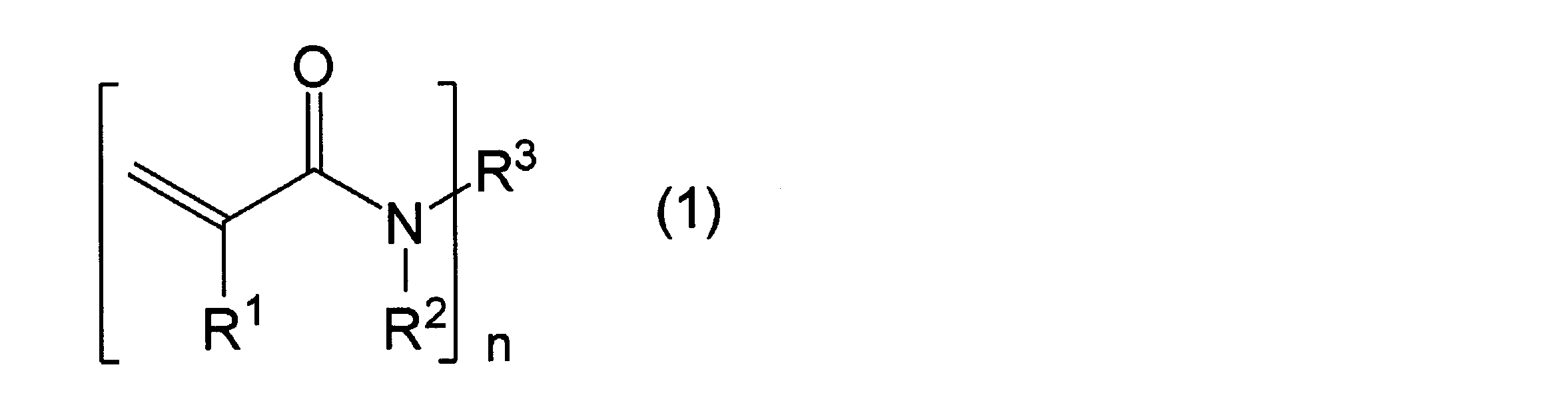
(式中、R1は水素原子又はメチル基を表し、R2は水素原子又は炭素原子数1乃至3のアルキル基を表し、nは1又は2を表し、
nが1の場合、
R3は、ヒドロキシ基、カルボキシ基、アセチル基、1つ又は2つの水素原子がメチル基で置換されていてもよいアミノ基、スルホ基、及び炭素原子数1乃至4のアルコキシ基からなる群から選択される少なくとも一つの置換基で置換されていてもよい、炭素原子数1乃至12のアルキル基を表し、
nが2の場合、
R3は、ヒドロキシ基、カルボキシ基、アセチル基、1つ又は2つの水素原子がメチル基で置換されていてもよいアミノ基、スルホ基、及び炭素原子数1乃至4のアルコキシ基からなる群から選択される少なくとも一つの置換基で置換されていてもよい、炭素原子数1乃至12のアルキレン基を表す。)
第2観点として、(A)成分が、(A)成分及び(B)成分の合計質量に基づいて0.05質量%以上10質量%以下の量にて含まれてなる、第1観点に記載のインプリント材料に関する。
第3観点として、(D)成分としてシリコーン化合物を更に含有する、第1観点又は第2観点に記載のインプリント材料に関する。
第4観点として、(E)成分として界面活性剤を更に含有する、第1観点乃至第3観点のいずれか一つに記載のインプリント材料に関する。
第5観点として、(F)成分として溶剤を更に含有する、第1観点乃至第4観点のいずれか一つに記載のインプリント材料に関する。
第6観点として、(B)成分が重合性基を2つ有する化合物である、第1観点乃至第5観点のいずれか一つに記載のインプリント材料に関する。
第7観点として、(B)成分がアクリロイルオキシ基、メタアクリロイルオキシ基、ビニル基及びアリル基からなる群から選ばれる少なくとも1種の重合性基を2つ有する化合物である、第1観点乃至第6観点のいずれか一つに記載のインプリント材料に関する。
第8観点として、第1観点乃至第7観点のいずれか一つに記載のインプリント材料から作製され、パターンが転写された膜に関する。
第9観点として、第8観点に記載のパターンが転写された膜を基材上に備えた光学部材に関する。
第10観点として、第8観点に記載のパターンが転写された膜を基材上に備えた固体撮像装置に関する。
第11観点として、第8観点に記載のパターンが転写された膜を基材上に備えたLEDデバイスに関する。
第12観点として、第8観点に記載のパターンが転写された膜を備えた半導体素子に関する。
第13観点として、第8観点に記載のパターンが転写された膜を基材上に備えた太陽電池に関する。
第14観点として、第8観点に記載のパターンが転写された膜を基材上に備えたディスプレイに関する。
第15観点として、第8観点に記載のパターンが転写された膜を基材上に備えた電子デバイスに関する。
また本発明のインプリント材料は、光硬化が可能であり、かつモールド面からの剥離時にパターンの一部に剥がれが生じないため、所望のパターンが正確に形成された膜が得られる。したがって、良好な光インプリントのパターン形成が可能である。
(A)成分の化合物は、下記式(1)で表される化合物であり、すなわちその構造内に(メタ)アクリルアミド構造を有する化合物である。
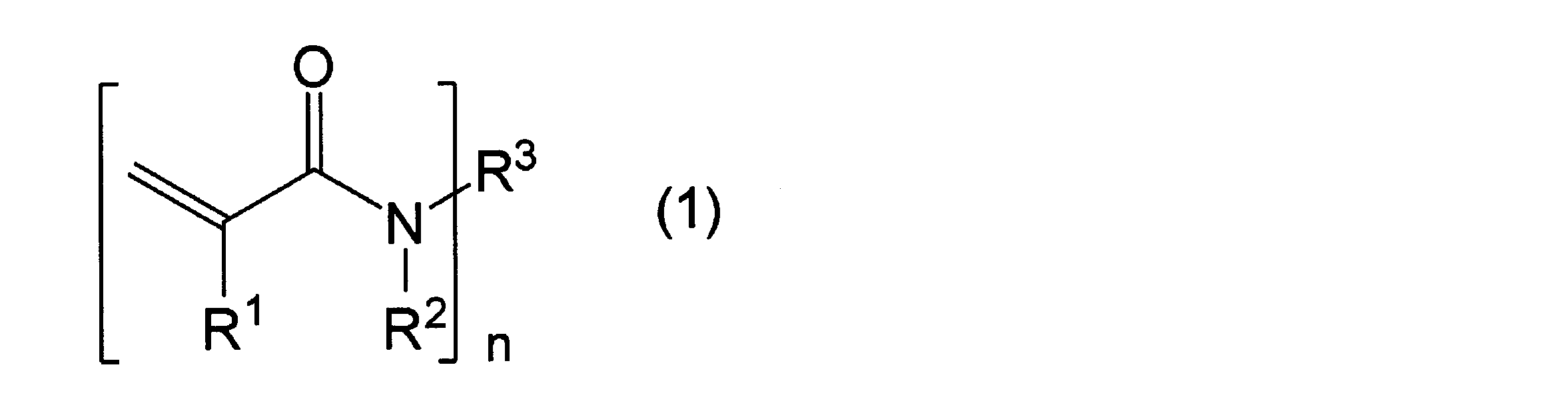
式(1)中、R1は水素原子又はメチル基を表し、R2は水素原子又は炭素原子数1乃至3のアルキル基を表し、nは1又は2を表す。
nが1の場合、R3は、ヒドロキシ基、カルボキシ基、アセチル基、1つ又は2つの水素原子がメチル基で置換されていてもよいアミノ基、スルホ基、及び炭素原子数1乃至4のアルコキシ基からなる群から選択される少なくとも一つの置換基で置換されていてもよい、炭素原子数1乃至12のアルキル基を表す。
またnが2の場合、R3は、ヒドロキシ基、カルボキシ基、アセチル基、1つ又は2つの水素原子がメチル基で置換されていてもよいアミノ基、スルホ基、及び炭素原子数1乃至4のアルコキシ基からなる群から選択される少なくとも一つの置換基で置換されていてもよい、炭素原子数1乃至12のアルキレン基を表す。
なお炭素原子数1乃至3のアルキル基の具体例としては、上記炭素原子数1乃至12のアルキル基として挙げた基のうち、炭素原子数が1乃至3の基を挙げることができる。
中でも、上記式(1)で表される化合物は、極少量の添加量で密着性を発現させる観点から、N,N’-ジメチル(メタ)アクリルアミド、N,N’-ジエチル(メタ)アクリルアミド、N,N’-(1,2-ジヒドロキシエチレン)ビス(メタ)アクリルアミドが好ましく、これらの中でもアクリルアミド化合物が最も好ましい。
(B)成分の化合物は、一分子内にプロピレンオキサイドユニットを1つ以上、エチレンオキサイドユニットを1つ以上、又はプロピレンオキサイドユニット及びエチレンオキサイドユニットをそれぞれ1つ以上有し、かつ重合性基を末端に2つ乃至6つ有する化合物を指す。
なお、上記プロピレンオキサイドユニットとは例えば(-CH(CH3)CH2O-)、(-CH2CH2CH2O-)を表し、上記エチレンオキサイドユニットとは例えば(-CH2CH2O-)を表す。
また当該重合性基としては、例えば、アクリロイルオキシ基、メタアクリロイルオキシ基、ビニル基、アリル基が挙げられる。ここで、アクリロイルオキシ基はアクリロキシ基と、メタアクリロイルオキシ基はメタアクリロキシ基と表現されることがある。
上記化合物は、市販品として入手が可能であり、その具体例としては、AM-30G、AM-90G、AM-130G、AM-230G、AMP-10G、AMP-20GY、AMP-60G、PHE-1G、A-200、A-400、A-600、A-1000、1G、2G、3G、4G、9G、14G、23G、ABE-300、A-BPE-4、A-BPE-6、A-BPE-10、A-BPE-20、A-BPE-30、BPE-80N、BPE-100N、BPE-200、BPE-500、BPE-900、BPE-1300N、A-GLY-3E、A-GLY-9E、A-GLY-20E、A-TMPT-3EO、A-TMPT-9EO、ATM-4E、ATM-35E、A-DPH-12E(以上、新中村化学工業株式会社製)、KAYARAD(登録商標)DPEA-12、同PEG400DA、同THE-330、同RP-1040(以上、日本化薬株式会社製)、M-210、M-350(以上、東亞合成株式会社製)が挙げられる。
上記化合物は、市販品として入手が可能であり、その具体例としては、APG-100、APG-200、APG-400、APG-700、3PG、9PG、A-DPH-6P(以上、新中村化学工業株式会社製)、ファンクリル(登録商標)FA-P240A、同FA-P270A、(以上、日立化成工業株式会社製)が挙げられる。
上記化合物は、市販品として入手が可能であり、その具体例としては、A-1000PER、A-B1206PE(以上、新中村化学工業株式会社製)、ファンクリル(登録商標)FA-023M(以上、日立化成工業株式会社製)が挙げられる。
また上記(B)成分の化合物の種類及び含有割合を変更することで、インプリント材料の動的粘度、インプリント時の硬化速度及び形成される膜厚をコントロールすることができる。
(A)成分の割合が0.05質量%未満であると、光インプリントにより得られる膜の基板に対する密着性が低下し、一方、10質量%を超えて添加すると、耐擦傷性が急激に低下する。
(C)成分である光重合開始剤は、光硬化時に使用する光源に吸収をもつものであれば、特に限定されるものではない。
例えば、tert-ブチルペルオキシ-iso-ブタレート、2,5-ジメチル-2,5-ビス(ベンゾイルジオキシ)ヘキサン、1,4-ビス[α-(tert-ブチルジオキシ)-iso-プロポキシ]ベンゼン、ジ-tert-ブチルペルオキシド、2,5-ジメチル-2,5-ビス(tert-ブチルジオキシ)ヘキセンヒドロペルオキシド、α-(iso-プロピルフェニル)-iso-プロピルヒドロペルオキシド、tert-ブチルヒドロペルオキシド、1,1-ビス(tert-ブチルジオキシ)-3,3,5-トリメチルシクロヘキサン、ブチル-4,4-ビス(tert-ブチルジオキシ)バレレート、シクロヘキサノンペルオキシド、2,2’,5,5’-テトラ(tert-ブチルペルオキシカルボニル)ベンゾフェノン、3,3’,4,4’-テトラ(tert-ブチルペルオキシカルボニル)ベンゾフェノン、3,3’,4,4’-テトラ(tert-アミルペルオキシカルボニル)ベンゾフェノン、3,3’,4,4’-テトラ(tert-ヘキシルペルオキシカルボニル)ベンゾフェノン、3,3’-ビス(tert-ブチルペルオキシカルボニル)-4,4’-ジカルボキシベンゾフェノン、tert-ブチルペルオキシベンゾエート、ジ-tert-ブチルジペルオキシイソフタレート等の有機過酸化物;9,10-アントラキノン、1-クロロアントラキノン、2-クロロアントラキノン、オクタメチルアントラキノン、1,2-ベンズアントラキノン等のキノン類;ベンゾインメチル、ベンゾインエチルエーテル、α-メチルベンゾイン、α-フェニルベンゾイン等のベンゾイン誘導体;2,2-ジメトキシ-1,2-ジフェニルエタン-1-オン、1-ヒドロキシ-シクロヘキシル-フェニル-ケトン、2-ヒドロキシ-2-メチル-1-フェニル-プロパン-1-オン、1-[4-(2-ヒドロキシエトキシ)-フェニル]-2-ヒドロキシ-2-メチル-1-プロパン-1-オン、2-ヒドロキシ-1-[4-{4-(2-ヒドロキシ-2-メチル-プロピオニル)ベンジル}-フェニル]-2-メチル-プロパン-1-オン、フェニルグリオキシリックアシッドメチルエステル、2-メチル-1-[4-(メチルチオ)フェニル]-2-モルホリノプロパン-1-オン、2-ベンジル-2-ジメチルアミノ-1-(4-モルホリノフェニル)-ブタン-1-オン、2-ジメチルアミノ-2-(4-メチル-ベンジル)-1-(4-モルホリン-4-イル-フェニル)-ブタン-1-オン等のアルキルフェノン系化合物;ビス(2,4,6-トリメチルベンゾイル)-フェニルホスフィンオキサイド、2,4,6-トリメチルベンゾイル-ジフェニル-ホスフィンオキサイド等のアシルホスフィンオキサイド系化合物;1,2-オクタンジオン,1-[4-(フェニルチオ)-,2-(O-ベンゾイルオキシム)]、エタノン,1-[9-エチル-6-(2-メチルベンゾイル)-9H-カルバゾール-3-イル]-,1-(O-アセチルオキシム)等のオキシムエステル系化合物が挙げられる。
(C)成分の含有量の割合が0.1phr未満の場合には、十分な硬化性が得られず、パターニング特性の悪化及び耐擦傷性の低下が起こるからである。本明細書において“phr”とは、例えば(A)成分及び(B)成分の総質量100gに対する、又は後述する(G)成分を含む場合には(A)成分及び(B)成分及び(G)成分の総質量100gに対する、光重合開始剤の質量を表す。
本発明においては、任意成分としてシリコーン化合物を含んでいてもよい。(D)成分であるシリコーン化合物は、分子内にシリコーン骨格(シロキサン骨格)を有する化合物を表し、特にジメチルシリコーン骨格を有することが好ましい。
本発明においては任意成分として界面活性剤を含んでいてもよい。(E)成分である界面活性剤は、得られる塗膜の製膜性を調整する役割を果たす。
界面活性剤が使用される場合、その割合は、上記(A)成分及び上記(B)成分の総質量に基づいて、又は後述する(G)成分を含む場合には(A)成分及び(B)成分及び(G)成分の総質量に基づいて、好ましくは0.01phr乃至40phr、より好ましくは0.01phr乃至10phrである。
本発明においては(F)成分として溶剤を含有してもよい。任意成分である(F)溶剤は、前記(A)成分及び(B)成分、並びに、又は後述する(G)成分を含む場合には(A)成分及び(B)成分及び(G)成分の粘度調節の役割を果たす。
溶剤が使用される場合、本発明のインプリント材料の全成分、すなわち前述の(A)成分乃至(C)成分、並びに後述するその他添加剤を含む全成分から(F)成分の溶剤を除いたものとして定義される固形分の割合が前記インプリント材料の総質量に対して20質量%乃至80質量%、好ましくは40質量%乃至60質量%となる量になるように、溶剤を含有することが好ましい。
本発明においては、その効果を損なわない限りにおいて、(G)成分として重合性基を末端に3つ以上有しアルキレンオキサイドユニットは有さない化合物を添加してもよい。(G)成分である重合性基を末端に3つ以上有しアルキレンオキサイドユニットは有さない化合物は、光インプリントにより得られる膜の硬度を調整する役割を果たす。当該重合性基としては、例えば、アクリロイルオキシ基、メタアクリロイルオキシ基、ビニル基、アリル基が挙げられる。
本発明のインプリント材料は、本発明の効果を損なわない限りにおいて、必要に応じて、エポキシ化合物、光酸発生剤、光増感剤、紫外線吸収剤、酸化防止剤、密着補助剤又は離型性向上剤を含有することができる。
光増感剤は、単独又は2種以上の組み合わせで使用することができる。当該光増感剤を用いることによって、UV領域の吸収波長を調整することもできる。
紫外線吸収剤は、単独又は2種以上の組み合わせで使用することができる。当該紫外線吸収剤を用いることによって、光硬化時に膜の最表面の硬化速度を制御することができ、離型性を向上できる場合がある。
酸化防止剤は、単独又は2種以上の組み合わせで使用することができる。当該酸化防止剤を用いることで、酸化によって膜が黄色に変色することを防止することができる。
当該密着補助剤の含有量は、上記(A)成分及び上記(B)成分の総質量に基づいて、又は前述の(G)成分を含む場合には(A)成分及び(B)成分及び(G)成分の総質量に基づいて、好ましくは5phr乃至50phr、より好ましくは10phr乃至50phrである。
本発明のインプリント材料の調製方法は、特に限定されないが、(A)成分、(B)成分、(C)成分、並びに任意成分である(D)成分、(E)成分、(F)成分及び(G)成分並びに所望によりその他添加剤を混合し、インプリント材料が均一な状態となっていればよい。
また、(A)成分乃至(G)成分並びに所望によりその他添加剤を混合する際の順序は、均一なインプリント材料が得られるなら問題なく、特に限定されない。当該調製方法としては、例えば、(A)成分に(B)成分を所定の割合で混合する方法が挙げられる。また、これに更に(C)成分、(D)成分、(E)成分、(F)成分、(G)成分を適宜混合し、均一なインプリント材料とする方法も挙げられる。さらに、この調製方法の適当な段階において、必要に応じて、その他の添加剤を更に添加して混合する方法が挙げられる。
本発明のインプリント材料は、基材上に塗布し光硬化させることで所望の被膜を得ることができる。塗布方法としては、公知又は周知の方法、例えば、スピンコート法、ディップ法、フローコート法、インクジェット法、スプレー法、バーコート法、グラビアコート法、スリットコート法、ロールコート法、転写印刷法、刷毛塗り、ブレードコート法、エアーナイフコート法を挙げることができる。
そして本発明のインプリント材料をフィルム上に塗布し、これをモールド面に接着させ、続いて該塗膜をモールド面を接着させたまま光硬化させ、その後フィルム上に硬化被膜をモールド面から90°剥離する試験において計測された離型力、すなわち、該フィルム上の被膜をモールド面から完全に剥離したときの荷重を該フィルムの横幅1cmあたりに換算した値が0g/cmより大きく0.5g/cm以下であることが好ましく、より好ましくは0.4g/cm以下である。
<実施例1>
KAYARAD(登録商標)DPEA-12(以下、本明細書では「DPEA-12」と略称する。)(日本化薬株式会社製)9.9g及びN,N’-ジメチルアクリルアミド(東京化成工業株式会社製)0.1gを混合し、その混合物にLucirin(登録商標)TPO(BASFジャパン株式会社製)(以下、本明細書では「Lucirin TPO」と略称する。)を0.25g(DPEA-12、N,N’-ジメチルアクリルアミドの総質量に対して2.5phr)加え、インプリント材料PNI-a1を調製した。
NKエステル A-200(以下、本明細書では「A-200」と略称する。)(新中村化学工業株式会社製)9.995g及びN,N’-ジメチルアクリルアミド0.005gを混合し、その混合物にLucirin TPOを0.25g(A-200、N,N’-ジメチルアクリルアミドの総質量に対して2.5phr)加え、インプリント材料PNI-a2を調製した。
A-200を9g及びN,N’-ジメチルアクリルアミド1gを混合し、その混合物にLucirin TPOを0.25g(A-200、N,N’-ジメチルアクリルアミドの総質量に対して2.5phr)加え、インプリント材料PNI-a3を調製した。
KAYARAD(登録商標)PET30(以下、本明細書では「PET30」と略称する。)(日本化薬株式会社製)1.5g、A-200を8g及びN,N’-ジメチルアクリルアミド0.5gを混合し、その混合物にLucirin TPOを0.25g(PET30、A-200、N,N’-ジメチルアクリルアミドの総質量に対して2.5phr)加え、インプリント材料PNI-a4を調製した。
A-200を6.5g、NKエコノマー A-1000PER(以下、本明細書では「A-1000PER」と略称する。)(新中村化学工業株式会社製)3g、N,N’-ジメチルアクリルアミドを0.5g及びBYK-333(ビックケミー・ジャパン株式会社製)0.1g(A-200、A1000PER、N,N’-ジメチルアクリルアミドの総質量に対して1phr)を混合し、その混合物にLucirin TPOを0.25g(A-200、A-1000PER、N,N’-ジメチルアクリルアミドの総質量に対して2.5phr)加え、インプリント材料PNI-a5を調製した。
A-200を5.5g、A-1000PERを4g、N,N’-ジメチルアクリルアミドを0.5g及びBYK-333を0.1g(A-200、A1000PER、N,N’-ジメチルアクリルアミドの総質量に対して1phr)混合し、その混合物にLucirin TPOを0.25g(A-200、A-1000PER、N,N’-ジメチルアクリルアミドの総質量に対して2.5phr)加え、インプリント材料PNI-a6を調製した。
DPEA-12を9.9g及びN,N’-ジエチルアクリルアミド(東京化成工業株式会社製)0.1gを混合し、その混合物にLucirin TPOを0.25g(DPEA-12、N,N’-ジエチルアクリルアミドの総質量に対して2.5phr)加え、インプリント材料PNI-a7を調製した。
DPEA-12を3.9g、A-200を3g、A-1000PERを3g、N,N’-ジエチルアクリルアミドを0.1g及びBYK-333を0.1g(DPEA-12、A-200、A1000PER、N,N’-ジエチルアクリルアミドの総質量に対して1phr)混合し、その混合物にLucirin TPOを0.25g(DPEA-12、A-200、A-1000PER、N,N’-ジエチルアクリルアミドの総質量に対して2.5phr)加え、インプリント材料PNI-a8を調製した。
A-200を5g、NKエステル APG-700(以下、本明細書では「APG-700」と略称する。)(新中村化学工業株式会社製)を4.5g及びN,N’-ジエチルアクリルアミドを0.5g混合し、その混合物にLucirin TPOを0.25g(A-200、APG-700、N,N’-ジエチルアクリルアミドの総質量に対して2.5phr)加え、インプリント材料PNI-a9を調製した。
A-200を7.99g、A1000PERを2g、N,N’-ジエチルアクリルアミドを0.01g及びBYK-333を0.1g(A-200、A1000PER、N,N’-ジエチルアクリルアミドの総質量に対して1phr)混合し、その混合物にLucirin TPOを0.25g(A-200、A-1000PER、N,N’-ジエチルアクリルアミドの総質量に対して2.5phr)加え、インプリント材料PNI-a10を調製した。
A-200を7.5g、A1000PERを2g、N,N’-ジエチルアクリルアミドを0.5g及びBYK-333を0.1g(A-200、A1000PER、N,N’-ジエチルアクリルアミドの総質量に対して1phr)混合し、その混合物にLucirin TPOを0.25g(A-200、A-1000PER、N,N’-ジエチルアクリルアミドの総質量に対して2.5phr)加え、インプリント材料PNI-a11を調製した。
DPEA-12を9.9g及びN,N’-(1,2-ジヒドロキシエチレン)ビスアクリルアミド(東京化成工業株式会社製)0.1gを混合し、その混合物にLucirin TPOを0.25g(DPEA-12、N,N’-(1,2-ジヒドロキシエチレン)ビスアクリルアミドの総質量に対して2.5phr)加え、インプリント材料PNI-a12を調製した。
A-200を5g、APG-700を4.5g、N,N’-(1,2-ジヒドロキシエチレン)ビスアクリルアミドを0.5及びBYK-333を0.1g(A-200、APG-700、N,N’-(1,2-ジヒドロキシエチレン)ビスアクリルアミドの総質量に対して1phr)混合し、その混合物にLucirin TPOを0.25g(A-200、A-1000PER、N,N’-(1,2-ジヒドロキシエチレン)ビスアクリルアミドの総質量に対して2.5phr)加え、インプリント材料PNI-a13を調製した。
A-200を7.5g、A-1000PERを2g、N,N’-(1,2-ジヒドロキシエチレン)ビスアクリルアミドを0.5g及びBYK-333を0.1g(A-200、A-1000PER、N,N’-(1,2-ジヒドロキシエチレン)ビスアクリルアミドの総質量に対して1phr)混合し、その混合物にLucirin TPOを0.25g(A-200、A-1000PER、N,N’-(1,2-ジヒドロキシエチレン)ビスアクリルアミドの総質量に対して2.5phr)加え、インプリント材料PNI-a14を調製した。
A-200を8.5g、A-1000PERを0.5g、N,N’-ジメチルアクリルアミドを1g及びBYK-333を0.1g(A-200、A-1000PER、N,N’-ジメチルアクリルアミドの総質量に対して1phr)混合し、その混合物にLucirin TPOを0.25g(A-200、A-1000PER、N,N’-ジメチルアクリルアミドの総質量に対して2.5phr)加え、インプリント材料PNI-a15を調製した。
A-200を8.9g、A-1000PERを0.1g、N,N’-ジメチルアクリルアミドを1g及びBYK-333を0.1g(A-200、A-1000PER、N,N’-ジメチルアクリルアミドの総質量に対して1phr)混合し、その混合物にLucirin TPOを0.25g(A-200、A-1000PER、N,N’-ジメチルアクリルアミドの総質量に対して2.5phr)加え、インプリント材料PNI-a16を調製した。
PET30を10g用意し、それにLucirin TPOを0.25g(PET30の総質量に対して2.5phr)加え、インプリント材料PNI-b1を調製した。
PET30を2g及びA-200を8g混合し、その混合物にLucirin TPOを0.25g(PET30、A-200の総質量に対して2.5phr)加え、インプリント材料PNI-b2を調製した。
A-200を6.5g及びA-1000PERを3.5g混合し、その混合物にLucirin TPOを0.25g(A-200、A-1000PERの総質量に対して2.5phr)加え、インプリント材料PNI-b3を調製した。
A-200を5.5g及びAPG-700を4.5g混合し、その混合物にLucirin TPOを0.25g(A-200、APG-700の総質量に対して2.5phr)加え、インプリント材料PNI-b4を調製した。
A-200を8.7g及びN,N’-ジメチルアクリルアミドを1.3g混合し、Lucirin TPOを0.25g(A-200、N,N’-ジメチルアクリルアミドの総質量に対して2.5phr)加え、インプリント材料PNI-b5を調製した。
A-200を5g、APG-700を3.7g及びN,N’-ジメチルアクリルアミドを1.3g混合し、その混合物にLucirin TPOを0.25g(A-200、APG-700、N,N’-ジメチルアクリルアミドの総質量に対して2.5phr)加え、インプリント材料PNI-b6を調製した。
A-200を5g、APG-700を3.7g、N,N’-ジメチルアクリルアミドを1.3g及びBYK-333を0.1g(A-200、APG-700、N,N’-ジメチルアクリルアミドの総質量に対して1phr)混合し、その混合物にLucirin TPOを0.25g(A-200、APG-700、N,N’-ジメチルアクリルアミドの総質量に対して2.5phr)加え、インプリント材料PNI-b7を調製した。
A-200を5g、APG-700を3.7g及びN,N’-ジエチルアクリルアミドを1.3g混合し、その混合物にLucirin TPOを0.25g(A-200、APG-700、N,N’-ジエチルアクリルアミドの総質量に対して2.5phr)加え、インプリント材料PNI-b8を調製した。
A-200を5g、APG-700を3.7g及びN,N’-(1,2-ジヒドロキシエチレン)ビスアクリルアミドを1.3g混合し、その混合物にLucirin TPOを0.25g(A-200、APG-700、N,N’-(1,2-ジヒドロキシエチレン)ビスアクリルアミドの総質量に対して2.5phr)加え、インプリント材料PNI-b9を調製した。
ニッケル製のピッチ250nm、高さ250nmのモスアイパターンモールド(株式会社イノックス製)及びシリコンウエハを、オプツール(登録商標)DSX(ダイキン工業株式会社製)をノベック(登録商標)HFE-7100(ハイドロフルオロエーテル、住友スリーエム株式会社)(以下、本明細書では「ノベックHFE-7100」と略称する。)で0.1質量%に希釈した溶液へ浸漬し、温度が90℃、湿度が90RH%の高温高湿装置を用いて1時間処理し、ノベックHFE-7100でリンス後、エアーで乾燥させた。
実施例1乃至実施例16及び比較例1乃至比較例9で得られた各インプリント材料を、厚さ80μmのトリアセチルセルロースフィルム(富士フイルム株式会社製 フジタック(登録商標)を使用)(以下、本明細書では「TACフィルム」と略称する。)上にバーコーター(全自動フィルムアプリケーター KT-AB3120 コーテック株式会社製)を用いて塗布し、そのTACフィルム上の塗膜を前述の離型処理を施したモスアイパターンモールドへローラー圧着させた。続いて該塗膜に対し、TACフィルム側から無電極均一照射装置(QRE-4016A、株式会社オーク製作所製)にて、350mJ/cm2の露光を施し、光硬化を行った。そしてJIS Z0237を参考にして90°剥離試験を行い、モールドの凹凸形状を有する面と接着している、TACフィルム上に形成された硬化被膜が、モールドの凹凸形状を有する面から完全に剥がれたときの荷重を測定した。そしてフィルムの幅1cm当たりの荷重を算出し、離型力(g/cm)とした。結果を表1に示す。
上記離型力試験後に得られた硬化被膜について、スチールウール擦傷試験を行った。試験機は大栄精機(有)製を使用し、♯0000のスチールウールを使用した。単位面積当たりの荷重は15g/cm2とし、上記スチールウールを10往復させ、擦傷後の傷本数を確認した。本擦傷試験を3回繰り返し、擦傷後の傷本数の平均値を算出し、以下のように評価した。
0~1本:A
2~5本:B
6~10本:C
11本以上:D
上記離型力試験後に得られた硬化被膜について、パターン形成膜とTACフィルムとの密着性試験を行った。密着性試験はJIS K5400に従い、以下の手順にて行った。
まず、パターン形成膜を、カッターを用いてTACフィルムに達する碁盤目状の切り傷を1mm間隔にて100マス付けた。約50mmの長さのセロハン粘着テープを碁盤目の上に粘着し、膜面に対して90°の角度で瞬間的に引き剥がした。
テープ剥離後のマス目を観察し、100マスに対して剥離しなかったマス目数をxとし、密着性をx/100として評価した。本密着性試験を3回繰り返し、各評価の平均値を算出した。得られた結果を表1に示す。
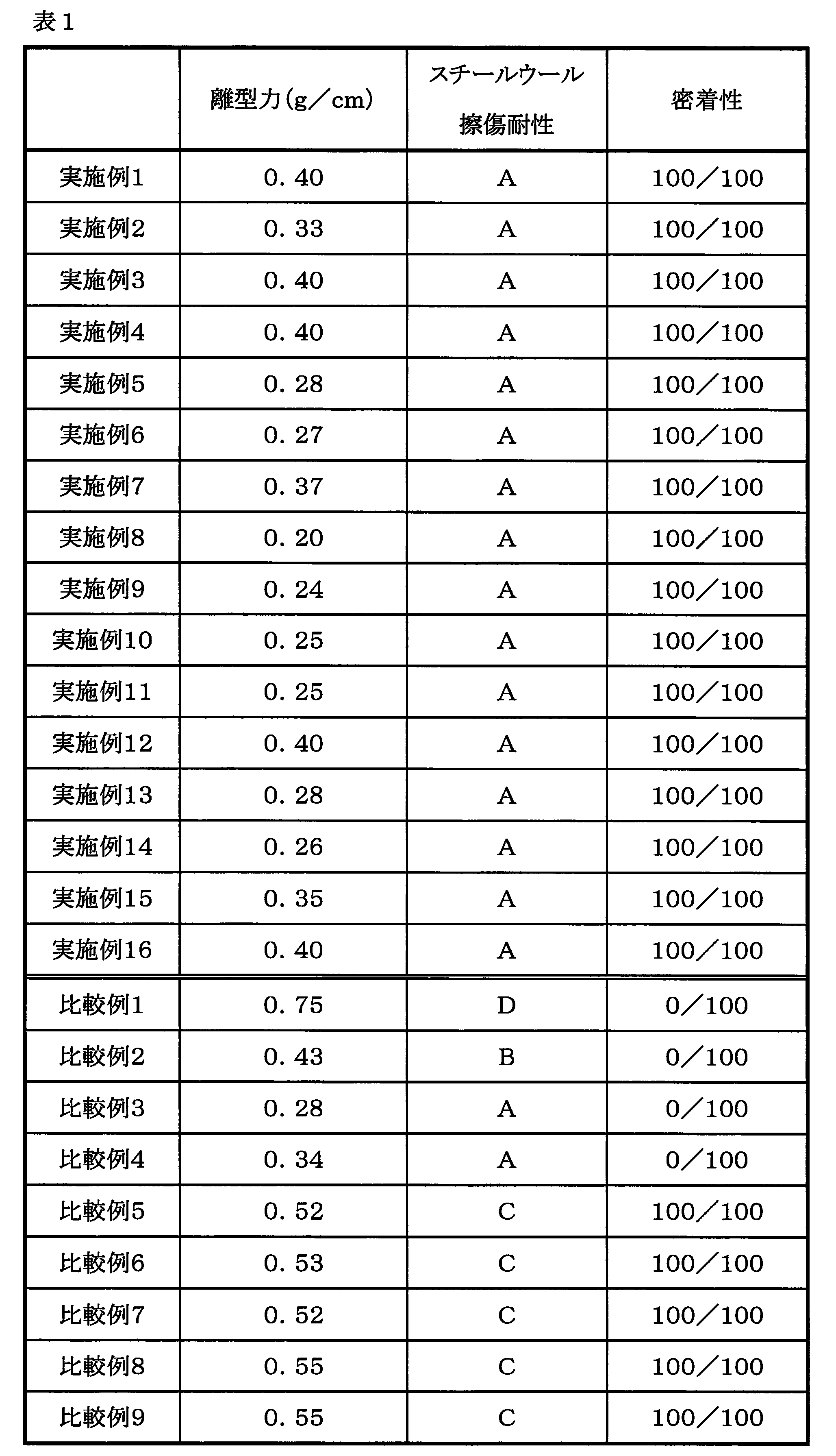
一方、アクリルアミド化合物を含有せず、また、アルキレンオキサイドユニットを有しない重合性化合物を用いた比較例1で得られたインプリント材料を用いた場合は、離型力が大きく、密着性に欠け、またスチールウール擦傷試験後に傷が多数発生した。
またアクリルアミド化合物を含有せずに調製した比較例2乃至比較例4で得られたインプリント材料を用いた場合は密着性に欠ける結果となった。
そしてアクリルアミド化合物の含有量を増やした比較例5乃至比較例9で得られたインプリント材料を用いた場合はスチールウール擦傷試験後に傷が多数発生した。
以上、本発明のインプリント材料により得られる膜は、低離型力性を有し、またインプリント後も耐擦傷性を有し、しかも基板に対する密着性に優れるものとなる。
Claims (15)
- 下記(A)成分、(B)成分、及び(C)成分を含有するインプリント材料。
(A)下記式(1)で表される化合物
(B)アルキレンオキサイドユニットを有しかつ重合性基を末端に2つ乃至6つ有する化合物であって、該アルキレンオキサイドユニットがエチレンオキサイドユニット、プロピレンオキサイドユニット、又はそれらの組み合わせである化合物
(C)光重合開始剤

(式中、R1は水素原子又はメチル基を表し、R2は水素原子又は炭素原子数1乃至3のアルキル基を表し、nは1又は2を表し、
nが1の場合、
R3は、ヒドロキシ基、カルボキシ基、アセチル基、1つ又は2つの水素原子がメチル基で置換されていてもよいアミノ基、スルホ基、及び炭素原子数1乃至4のアルコキシ基からなる群から選択される少なくとも一つの置換基で置換されていてもよい、炭素原子数1乃至12のアルキル基を表し、
nが2の場合、
R3は、ヒドロキシ基、カルボキシ基、アセチル基、1つ又は2つの水素原子がメチル基で置換されていてもよいアミノ基、スルホ基、及び炭素原子数1乃至4のアルコキシ基からなる群から選択される少なくとも一つの置換基で置換されていてもよい、炭素原子数1乃至12のアルキレン基を表す。) - (A)成分が、(A)成分及び(B)成分の合計質量に基づいて0.05質量%以上10質量%以下の量にて含まれてなる、請求項1に記載のインプリント材料。
- (D)成分としてシリコーン化合物を更に含有する、請求項1又は請求項2に記載のインプリント材料。
- (E)成分として界面活性剤を更に含有する、請求項1乃至請求項3のいずれか一項に記載のインプリント材料。
- (F)成分として溶剤を更に含有する、請求項1乃至請求項4のいずれか一項に記載のインプリント材料。
- (B)成分が重合性基を2つ有する化合物である、請求項1乃至請求項5のいずれか一項に記載のインプリント材料。
- (B)成分がアクリロイルオキシ基、メタアクリロイルオキシ基、ビニル基及びアリル基からなる群から選ばれる少なくとも1種の重合性基を2つ有する化合物である、請求項1乃至請求項6のいずれか一項に記載のインプリント材料。
- 請求項1乃至請求項7のいずれか一項に記載のインプリント材料から作製され、パターンが転写された膜。
- 請求項8に記載のパターンが転写された膜を基材上に備えた光学部材。
- 請求項8に記載のパターンが転写された膜を基材上に備えた固体撮像装置。
- 請求項8に記載のパターンが転写された膜を基材上に備えたLEDデバイス。
- 請求項8に記載のパターンが転写された膜を備えた半導体素子。
- 請求項8に記載のパターンが転写された膜を基材上に備えた太陽電池。
- 請求項8に記載のパターンが転写された膜を基材上に備えたディスプレイ。
- 請求項8に記載のパターンが転写された膜を基材上に備えた電子デバイス。
Priority Applications (4)
| Application Number | Priority Date | Filing Date | Title |
|---|---|---|---|
| JP2015512393A JP6238026B2 (ja) | 2013-04-18 | 2014-03-28 | インプリント材料 |
| KR1020157024723A KR20160002707A (ko) | 2013-04-18 | 2014-03-28 | 임프린트 재료 |
| US14/784,400 US9778564B2 (en) | 2013-04-18 | 2014-03-28 | Imprint material |
| CN201480021778.9A CN105210174B (zh) | 2013-04-18 | 2014-03-28 | 压印材料 |
Applications Claiming Priority (4)
| Application Number | Priority Date | Filing Date | Title |
|---|---|---|---|
| JP2013087545 | 2013-04-18 | ||
| JP2013-087545 | 2013-04-18 | ||
| JP2013-125807 | 2013-06-14 | ||
| JP2013125807 | 2013-06-14 |
Publications (1)
| Publication Number | Publication Date |
|---|---|
| WO2014171302A1 true WO2014171302A1 (ja) | 2014-10-23 |
Family
ID=51731254
Family Applications (1)
| Application Number | Title | Priority Date | Filing Date |
|---|---|---|---|
| PCT/JP2014/059205 Ceased WO2014171302A1 (ja) | 2013-04-18 | 2014-03-28 | インプリント材料 |
Country Status (6)
| Country | Link |
|---|---|
| US (1) | US9778564B2 (ja) |
| JP (1) | JP6238026B2 (ja) |
| KR (1) | KR20160002707A (ja) |
| CN (1) | CN105210174B (ja) |
| TW (1) | TWI610946B (ja) |
| WO (1) | WO2014171302A1 (ja) |
Cited By (2)
| Publication number | Priority date | Publication date | Assignee | Title |
|---|---|---|---|---|
| CN107710385A (zh) * | 2015-06-29 | 2018-02-16 | 日产化学工业株式会社 | 压印材料 |
| JP2018079617A (ja) * | 2016-11-16 | 2018-05-24 | リケンテクノス株式会社 | 表面に微細凹凸構造を有する塗膜 |
Families Citing this family (6)
| Publication number | Priority date | Publication date | Assignee | Title |
|---|---|---|---|---|
| CN109195999B (zh) * | 2016-05-11 | 2021-04-16 | Dic株式会社 | 光压印用固化性组合物及使用其的图案形成方法 |
| CN109563194B (zh) * | 2016-08-10 | 2021-06-22 | 日产化学株式会社 | 压印材料 |
| WO2018159575A1 (ja) | 2017-02-28 | 2018-09-07 | 富士フイルム株式会社 | インプリント用密着膜形成用組成物、密着膜、積層体、硬化物パターンの製造方法および回路基板の製造方法 |
| CA3093719A1 (en) | 2018-03-28 | 2019-10-03 | Basf Coatings Gmbh | Method for transferring an embossed structure to the surface of a coating means and compound structure usable as an embossing die |
| ES2971522T3 (es) | 2019-09-25 | 2024-06-05 | Basf Coatings Gmbh | Método para transferir una estructura grabada a la superficie de un recubrimiento, y material compuesto empleable como molde de grabado |
| GB202004794D0 (en) * | 2020-04-01 | 2020-05-13 | Fujifilm Mfg Europe Bv | Gas-separation membranes |
Citations (4)
| Publication number | Priority date | Publication date | Assignee | Title |
|---|---|---|---|---|
| JP2008019292A (ja) * | 2006-07-10 | 2008-01-31 | Fujifilm Corp | 光硬化性組成物およびそれを用いたパターン形成方法 |
| JP2008105414A (ja) * | 2006-09-27 | 2008-05-08 | Fujifilm Corp | 光ナノインプリントリソグラフィ用硬化性組成物およびそれを用いたパターン形成方法 |
| JP2008202022A (ja) * | 2007-01-23 | 2008-09-04 | Fujifilm Corp | 光ナノインプリントリソグラフィ用硬化性組成物およびそれを用いたパターン形成方法 |
| JP2012041521A (ja) * | 2010-05-12 | 2012-03-01 | Fujifilm Corp | 光硬化性組成物およびそれを用いた硬化物の製造方法 |
Family Cites Families (6)
| Publication number | Priority date | Publication date | Assignee | Title |
|---|---|---|---|---|
| US5772905A (en) | 1995-11-15 | 1998-06-30 | Regents Of The University Of Minnesota | Nanoimprint lithography |
| JP4906416B2 (ja) * | 2006-07-11 | 2012-03-28 | 日本碍子株式会社 | 物体の通過検出装置 |
| KR101463849B1 (ko) * | 2006-09-27 | 2014-12-04 | 후지필름 가부시키가이샤 | 광 나노임프린트 리소그래피용 경화성 조성물 및 그것을사용한 패턴 형성 방법 |
| JP2010000612A (ja) * | 2008-06-18 | 2010-01-07 | Fujifilm Corp | ナノインプリント用硬化性組成物、パターン形成方法 |
| WO2011132616A1 (ja) * | 2010-04-19 | 2011-10-27 | 日産化学工業株式会社 | 高耐擦傷性インプリント材料 |
| CN103503115B (zh) * | 2012-04-27 | 2016-01-13 | 日产化学工业株式会社 | 压印材料 |
-
2014
- 2014-03-28 JP JP2015512393A patent/JP6238026B2/ja active Active
- 2014-03-28 US US14/784,400 patent/US9778564B2/en not_active Expired - Fee Related
- 2014-03-28 WO PCT/JP2014/059205 patent/WO2014171302A1/ja not_active Ceased
- 2014-03-28 KR KR1020157024723A patent/KR20160002707A/ko not_active Withdrawn
- 2014-03-28 CN CN201480021778.9A patent/CN105210174B/zh not_active Expired - Fee Related
- 2014-04-14 TW TW103113544A patent/TWI610946B/zh not_active IP Right Cessation
Patent Citations (4)
| Publication number | Priority date | Publication date | Assignee | Title |
|---|---|---|---|---|
| JP2008019292A (ja) * | 2006-07-10 | 2008-01-31 | Fujifilm Corp | 光硬化性組成物およびそれを用いたパターン形成方法 |
| JP2008105414A (ja) * | 2006-09-27 | 2008-05-08 | Fujifilm Corp | 光ナノインプリントリソグラフィ用硬化性組成物およびそれを用いたパターン形成方法 |
| JP2008202022A (ja) * | 2007-01-23 | 2008-09-04 | Fujifilm Corp | 光ナノインプリントリソグラフィ用硬化性組成物およびそれを用いたパターン形成方法 |
| JP2012041521A (ja) * | 2010-05-12 | 2012-03-01 | Fujifilm Corp | 光硬化性組成物およびそれを用いた硬化物の製造方法 |
Cited By (3)
| Publication number | Priority date | Publication date | Assignee | Title |
|---|---|---|---|---|
| CN107710385A (zh) * | 2015-06-29 | 2018-02-16 | 日产化学工业株式会社 | 压印材料 |
| JPWO2017002506A1 (ja) * | 2015-06-29 | 2018-04-26 | 日産化学工業株式会社 | インプリント材料 |
| JP2018079617A (ja) * | 2016-11-16 | 2018-05-24 | リケンテクノス株式会社 | 表面に微細凹凸構造を有する塗膜 |
Also Published As
| Publication number | Publication date |
|---|---|
| KR20160002707A (ko) | 2016-01-08 |
| CN105210174B (zh) | 2018-01-30 |
| JP6238026B2 (ja) | 2017-11-29 |
| US20160068674A1 (en) | 2016-03-10 |
| CN105210174A (zh) | 2015-12-30 |
| US9778564B2 (en) | 2017-10-03 |
| JPWO2014171302A1 (ja) | 2017-02-23 |
| TWI610946B (zh) | 2018-01-11 |
| TW201500383A (zh) | 2015-01-01 |
Similar Documents
| Publication | Publication Date | Title |
|---|---|---|
| JP6238026B2 (ja) | インプリント材料 | |
| KR102121762B1 (ko) | 방오성을 갖는 요철형상의 표면을 갖는 구조체 및 그 제조방법 | |
| JP5263560B2 (ja) | 高硬度インプリント材料 | |
| JP6429031B2 (ja) | シルセスキオキサン化合物及び変性シリコーン化合物を含むインプリント材料 | |
| JP6015937B2 (ja) | 高耐擦傷性インプリント材料 | |
| WO2013161627A1 (ja) | インプリント材料 | |
| JP6338061B2 (ja) | 低離型力性を有するインプリント材料 | |
| WO2017110697A1 (ja) | インプリント材料 | |
| WO2017002506A1 (ja) | インプリント材料 | |
| JP6061073B2 (ja) | インプリント材料 |
Legal Events
| Date | Code | Title | Description |
|---|---|---|---|
| 121 | Ep: the epo has been informed by wipo that ep was designated in this application |
Ref document number: 14785779 Country of ref document: EP Kind code of ref document: A1 |
|
| ENP | Entry into the national phase |
Ref document number: 2015512393 Country of ref document: JP Kind code of ref document: A |
|
| ENP | Entry into the national phase |
Ref document number: 20157024723 Country of ref document: KR Kind code of ref document: A |
|
| WWE | Wipo information: entry into national phase |
Ref document number: 14784400 Country of ref document: US |
|
| NENP | Non-entry into the national phase |
Ref country code: DE |
|
| 122 | Ep: pct application non-entry in european phase |
Ref document number: 14785779 Country of ref document: EP Kind code of ref document: A1 |