WO2014162798A1 - 表示パネル及び表示装置 - Google Patents
表示パネル及び表示装置 Download PDFInfo
- Publication number
- WO2014162798A1 WO2014162798A1 PCT/JP2014/054544 JP2014054544W WO2014162798A1 WO 2014162798 A1 WO2014162798 A1 WO 2014162798A1 JP 2014054544 W JP2014054544 W JP 2014054544W WO 2014162798 A1 WO2014162798 A1 WO 2014162798A1
- Authority
- WO
- WIPO (PCT)
- Prior art keywords
- liquid crystal
- crystal panel
- substrate
- transparent
- view
- Prior art date
- Legal status (The legal status is an assumption and is not a legal conclusion. Google has not performed a legal analysis and makes no representation as to the accuracy of the status listed.)
- Ceased
Links
Images



Classifications
-
- G—PHYSICS
- G02—OPTICS
- G02F—OPTICAL DEVICES OR ARRANGEMENTS FOR THE CONTROL OF LIGHT BY MODIFICATION OF THE OPTICAL PROPERTIES OF THE MEDIA OF THE ELEMENTS INVOLVED THEREIN; NON-LINEAR OPTICS; FREQUENCY-CHANGING OF LIGHT; OPTICAL LOGIC ELEMENTS; OPTICAL ANALOGUE/DIGITAL CONVERTERS
- G02F1/00—Devices or arrangements for the control of the intensity, colour, phase, polarisation or direction of light arriving from an independent light source, e.g. switching, gating or modulating; Non-linear optics
- G02F1/01—Devices or arrangements for the control of the intensity, colour, phase, polarisation or direction of light arriving from an independent light source, e.g. switching, gating or modulating; Non-linear optics for the control of the intensity, phase, polarisation or colour
- G02F1/13—Devices or arrangements for the control of the intensity, colour, phase, polarisation or direction of light arriving from an independent light source, e.g. switching, gating or modulating; Non-linear optics for the control of the intensity, phase, polarisation or colour based on liquid crystals, e.g. single liquid crystal display cells
- G02F1/133—Constructional arrangements; Operation of liquid crystal cells; Circuit arrangements
- G02F1/1333—Constructional arrangements; Manufacturing methods
- G02F1/1335—Structural association of cells with optical devices, e.g. polarisers or reflectors
- G02F1/133528—Polarisers
-
- G—PHYSICS
- G02—OPTICS
- G02F—OPTICAL DEVICES OR ARRANGEMENTS FOR THE CONTROL OF LIGHT BY MODIFICATION OF THE OPTICAL PROPERTIES OF THE MEDIA OF THE ELEMENTS INVOLVED THEREIN; NON-LINEAR OPTICS; FREQUENCY-CHANGING OF LIGHT; OPTICAL LOGIC ELEMENTS; OPTICAL ANALOGUE/DIGITAL CONVERTERS
- G02F1/00—Devices or arrangements for the control of the intensity, colour, phase, polarisation or direction of light arriving from an independent light source, e.g. switching, gating or modulating; Non-linear optics
- G02F1/01—Devices or arrangements for the control of the intensity, colour, phase, polarisation or direction of light arriving from an independent light source, e.g. switching, gating or modulating; Non-linear optics for the control of the intensity, phase, polarisation or colour
- G02F1/13—Devices or arrangements for the control of the intensity, colour, phase, polarisation or direction of light arriving from an independent light source, e.g. switching, gating or modulating; Non-linear optics for the control of the intensity, phase, polarisation or colour based on liquid crystals, e.g. single liquid crystal display cells
- G02F1/133—Constructional arrangements; Operation of liquid crystal cells; Circuit arrangements
- G02F1/1333—Constructional arrangements; Manufacturing methods
- G02F1/1335—Structural association of cells with optical devices, e.g. polarisers or reflectors
- G02F1/133509—Filters, e.g. light shielding masks
- G02F1/133514—Colour filters
-
- G—PHYSICS
- G02—OPTICS
- G02F—OPTICAL DEVICES OR ARRANGEMENTS FOR THE CONTROL OF LIGHT BY MODIFICATION OF THE OPTICAL PROPERTIES OF THE MEDIA OF THE ELEMENTS INVOLVED THEREIN; NON-LINEAR OPTICS; FREQUENCY-CHANGING OF LIGHT; OPTICAL LOGIC ELEMENTS; OPTICAL ANALOGUE/DIGITAL CONVERTERS
- G02F1/00—Devices or arrangements for the control of the intensity, colour, phase, polarisation or direction of light arriving from an independent light source, e.g. switching, gating or modulating; Non-linear optics
- G02F1/01—Devices or arrangements for the control of the intensity, colour, phase, polarisation or direction of light arriving from an independent light source, e.g. switching, gating or modulating; Non-linear optics for the control of the intensity, phase, polarisation or colour
- G02F1/13—Devices or arrangements for the control of the intensity, colour, phase, polarisation or direction of light arriving from an independent light source, e.g. switching, gating or modulating; Non-linear optics for the control of the intensity, phase, polarisation or colour based on liquid crystals, e.g. single liquid crystal display cells
- G02F1/133—Constructional arrangements; Operation of liquid crystal cells; Circuit arrangements
- G02F1/1333—Constructional arrangements; Manufacturing methods
- G02F1/1335—Structural association of cells with optical devices, e.g. polarisers or reflectors
- G02F1/133528—Polarisers
- G02F1/133538—Polarisers with spatial distribution of the polarisation direction
Definitions
- the present invention relates to a display panel and a display device such as a liquid crystal panel and an organic EL panel.
- a transparent display that can see objects behind the display is drawing attention.
- transparency that is an index of light transmittance of the display and visibility that is an index of clarity of an object that can be seen through the display are required.
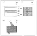
- FIG. 10 is a schematic view showing a conventional liquid crystal panel, (a) is a cross-sectional view of the conventional liquid crystal panel, (b) is a plan view showing a configuration of a color filter of the conventional liquid crystal panel, c) is a schematic diagram showing the visibility when used as a transparent display of a conventional liquid crystal panel.
- the liquid crystal panel 600 includes a TFT substrate 610 and a counter substrate 620, and a large number of subpixels are defined in plan view.
- Pixel electrodes (not shown) are provided corresponding to the sub-pixels
- the counter substrate 620 is provided with a color filter layer 625 having a colored portion at a position corresponding to the sub-pixels.
- polarizing layers 612 and 622 are provided over the entire surface of the TFT substrate 610 and the counter substrate 620.
- a conventional liquid crystal display device includes a light source, a drive circuit, and a liquid crystal panel, and performs full color display by controlling the transmittance of light emitted from the light source for each sub-pixel.
- the transmittance of the entire liquid crystal panel is about 10% of the light emitted from the light source.
- Patent Document 1 describes a transflective liquid crystal display device in which a part of a color filter is colorless.
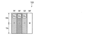
- FIG. 11 is a plan view showing the configuration of the color filter of the transflective liquid crystal display device of Patent Document 1.
- the transflective liquid crystal display device of Patent Document 1 has pixels composed of three color subpixels of R, G, and B and a fourth subpixel of colorless (W), and each subpixel has a reflection area RA and a transmission area.
- the color filter 725 has four filter segments Rf, Gf, Bf, and Mf corresponding to each subpixel.
- the filter segments Rf, Gf, and Bf are color filter segments that partially have colorless sub-segments Ws, and the filter segment Mf is a colorless (transparent) filter segment. Since the transflective liquid crystal display device of Patent Document 1 has a colorless filter segment Mf in the color filter 725, the reflectance can be improved.
- Patent Document 2 in order to display a predetermined pattern regardless of whether the power is on or off, a position corresponding to the predetermined pattern is set as a light reflection region, and a polarizing plate in the light reflection region is provided.
- the deleted liquid crystal display device is described.
- Japanese Patent Publication Japanese Patent Laid-Open No. 2011-128652” (published on June 30, 2011) Japanese Patent Publication “Japanese Unexamined Patent Application Publication No. 2009-157297 (Published July 16, 2009)”
- the transflective liquid crystal display device of Patent Document 1 a part of the color filter is colorless, but the polarizing plate is provided over the entire surface of the TFT substrate and the counter substrate as in the conventional liquid crystal display device.
- the light transmittance of the liquid crystal panel is insufficient for use as a transparent display.
- the liquid crystal display device of Patent Document 2 removes the polarizing plate in accordance with the predetermined pattern in order to display the predetermined pattern, the light transmittance of the liquid crystal panel is not uniform in plan view. For this reason, when the liquid crystal display device of Patent Document 2 is used as a transparent display, the contrast of the boundary portion of the object seen through the display is low, and the visibility is insufficient.
- the present invention has been made in view of the above problems, and an object thereof is to provide a display panel in which the light transmittance of the display panel is uniformly improved in a plan view and a display device using the display panel. .
- a display panel includes a first substrate and a second substrate provided to face each other, and the first substrate and the second substrate. At least one of them is a display panel provided with a polarizing layer, and the polarizing layer is provided with a polarizing region provided with a polarizing plate and the polarizing plate in a plan view. The transmission region is uniformly arranged in a plan view.
- the present invention by improving the light transmittance of the display panel uniformly in a plan view, it is possible to improve the visibility when an object on the back is viewed through the display panel.
- a liquid crystal panel will be described as an example of the display panel of the present invention.
- the present invention is not limited to this, and the present invention can also be applied to an organic EL panel.
- the manufacturing cost can be reduced.
- FIG. 1A and 1B are schematic views of a liquid crystal panel according to Embodiment 1, wherein FIG. 1A is a cross-sectional view of the liquid crystal panel, FIG. 1B is a plan view illustrating a configuration of a color filter layer, and FIG. FIG. 6D is a schematic diagram showing the visibility when the liquid crystal panel is used as a transparent display.
- the liquid crystal panel 1 includes a TFT substrate 10 (first substrate), a counter substrate 20 (second substrate) provided facing the TFT substrate 10, and a TFT substrate 10.
- the liquid crystal layer 30 is sandwiched between the counter substrate 20.
- liquid crystal layer 30 nematic liquid crystal or polymer network type liquid crystal can be used. Further, as the liquid crystal mode, TN (Twisted Nematic), VA (Vertical Alignment), ECB (Electrically Controlled Birefringence), OCB (Optically Compensated Bend), IPS (Sw-Inch, etc.) can be used.
- TN Transmission Nematic
- VA Very Alignment
- ECB Electrodefringence
- OCB Optically Compensated Bend
- IPS Sw-Inch, etc.
- the liquid crystal panel 1 has a plurality of sub-pixels defined in a matrix shape in plan view, and can display an image by controlling light emitted from each sub-pixel.
- the subpixels of the liquid crystal panel 1 include colored subpixels and transparent subpixels.
- the colored subpixel includes a red subpixel that emits red light, a green subpixel that emits green light, and a blue subpixel that emits blue light.
- liquid crystal display device combining a drive circuit and a light source with the liquid crystal panel 1 of this embodiment.
- a light source what is generally used for the conventional liquid crystal display device can be adopted, or natural light may be used as the light source.
- the TFT substrate 10 has a configuration in which a pixel electrode 14 is formed on the opposite substrate 20 side of the glass substrate 11 and a first polarizing layer 12 is formed on the opposite side of the glass substrate 11 from the opposite substrate 20.
- each sub-pixel of the liquid crystal panel 1 is illustrated by a broken line.
- a plurality of scanning signal lines 16 and a plurality of data signal lines 15 are formed in regions on the glass substrate 11 corresponding to the colored sub-pixels 60R, 60G, and 60B in plan view.
- a TFT is provided at the intersection of the scanning signal line 16 and the data signal line 15.
- a pixel electrode 14 is provided on the glass substrate 11 so as to overlap the colored subpixels 60R, 60G, and 60B, and the pixel electrode 14 and the TFT are electrically connected.
- a transparent conductive film such as ITO or IZO can be used as the pixel electrode 14 forms a liquid crystal capacitor LC and an auxiliary capacitor CS between the counter electrode 24 described later.
- no TFT or pixel electrode 14 is provided in a region on the glass substrate 11 that overlaps the transparent sub-pixel 60T in plan view.
- the 1st polarizing layer 12 contains the 1st polarizing plate 13, and the 1st polarizing plate 13 provided with the 1st polarizing plate 13 in planar view, and 1st And a transmission region where the polarizing plate 13 is not provided.
- the first polarizing plate 13 has a transmission axis in the direction of the arrow shown in FIG.
- a region that overlaps the colored sub-pixel in a plan view is a polarization region
- a region that overlaps the transparent sub-pixel is a transmission region.
- the pixel electrode 14 is not provided in a region overlapping the transmission region in plan view, and the pixel electrode 14 is provided in a region overlapping the polarization region.
- the color filter layer 25 is formed on the TFT substrate 10 side of the glass substrate 21
- the counter electrode 24 is formed on the color filter layer 25, and the second polarization is formed on the opposite side of the glass substrate 21 from the TFT substrate 10.
- the layer 22 is formed.
- the color filter layer 25 includes a colored portion 25R that transmits red light, a colored portion 25G that transmits green light, and a colored portion 25B that transmits blue light. It has a transparent portion 25T that transmits all visible light as it is.
- the color filter layer 25 includes a plurality of colored portions 25R, 25G, and 25B and transparent portions 25T that transmit light of different wavelengths, and the colored portions 25R, 25G, and 25B and the transparent portions 25T. Are lined up in this order.
- the colored portions 25R, 25G, and 25B are disposed so as to face the pixel electrode 14 of the TFT substrate 10, and the transparent portion 25T is disposed so as to face the region of the TFT substrate 10 where the pixel electrode 14 is not provided. .
- a transparent conductive film such as ITO or IZO can be used.
- a color resist ink can be used.
- a pigment can be suitably used since it is excellent in light resistance, heat resistance and solvent resistance.
- the second polarizing layer 22 includes a second polarizing plate 23, and in a plan view, a polarizing region where the second polarizing plate 23 is provided, and a second polarizing plate. And a transmission region in which 23 is not provided.
- the second polarizing plate 23 has a transmission axis in the direction of the arrow shown in FIG.
- the transmission axis of the first polarizing plate 13 and the polarization axis of the second polarizing plate 23 are orthogonal to each other.
- the liquid crystal panel 1 is a normally white liquid crystal panel. Although not shown, a normally black liquid crystal panel may be used.
- a region that overlaps the colored sub-pixel in a plan view is a polarization region, and a region that overlaps the transparent sub-pixel is a transmission region.
- colored regions 25R, 25G, and 25B are provided in regions overlapping the colored sub-pixels in a plan view, and transparent portions 25T are provided in regions overlapping the transparent sub-pixels.
- the colored sub-pixels of the liquid crystal panel 1 in the plan view overlap the polarizing region of the first polarizing layer 12 and the polarizing region of the second polarizing layer 22, and the colored portions 25R and 25G of the color filter layer 25 are overlapped. ⁇ It overlaps 25B.
- the transparent subpixel of the liquid crystal panel 1 overlaps the transmission region of the first polarizing layer 12 and the transmission region of the second polarizing layer 22 in plan view, and overlaps the transparent portion 25T of the color filter layer 25. .
- Method for forming polarizing layer As a method for forming the first polarizing layer 12 and the second polarizing layer 22, the following methods can be employed.
- a polarizing plate having absorption dichroism is formed by dyeing / adsorbing a dichroic material such as iodine or an organic dye on a base film (polyvinyl alcohol: PVA) and stretching / orienting it.
- a polarizing plate is bonded to the glass substrates 21 and 11, and unnecessary portions of the polarizing plate are removed along the transmission region using a wheel cutter or the like. Thereby, the 1st polarizing layer 12 and the 2nd polarizing layer 22 can be formed.
- the following methods can be adopted.
- a composition containing a liquid crystal compound and a dichroic dye is formed on the glass substrates 21 and 11.
- pattern exposure is performed on a region where birefringence or polarization is desired to remain.
- a pattern exposure method contact exposure using a mask, proxy exposure, projection exposure, or the like may be used, or direct drawing may be performed by focusing on a predetermined position without using a mask using a laser or an electron beam.
- a polarizing plate having polarization can be formed on the TFT substrate 10 or the counter substrate 20 so as to have a uniform pattern.
- the display size is 886.8 ⁇ 498.8 mm
- the sub-pixel size is approximately 115.5 ⁇ m
- the size of the colored sub-pixel and the transparent sub-pixel) is about 462 ⁇ m.
- the polarizing layer is bonded in a size according to the display size, and a wheel cutter or the like is used. Unnecessary portions of the polarizing plate are removed along the transparent pixel region. The thickness of the polarizing layer is about 0.2 mm.
- the transparent portion 25T of the color filter layer 25 overlaps the transmission region of the polarizing layer and the colored portions 25R, 25G, and 25B of the color filter layer 25 overlap the polarizing region of the polarizing layer in plan view.
- the transmission region only the central 100 mm ⁇ 100 mm portion of the liquid crystal panel 1 may be used as the transmission region.
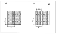
- FIG. 2 is a plan view showing the configuration of the color filter layer, (a) is a plan view of a color filter of a conventional liquid crystal panel, and (b) is a plan view of the color filter of the liquid crystal panel of the present embodiment. is there.
- the light transmittance of a conventional liquid crystal panel having the color filter layer shown in FIG. 2A and having a polarizing layer on the entire surface of the TFT substrate and the counter substrate is obtained as follows.
- Light transmittance (light transmittance of the R colored portion ⁇ area ratio of the R colored portion + light transmittance of the G colored portion ⁇ area ratio of the G colored portion + light transmittance of the B colored portion ⁇ area ratio of the B colored portion) ⁇ polarized light
- the light transmittance of the colored portion of each color of the color filter layer is 33%
- the light transmittance of the polarizing layer is 42%.
- the light transmittance of the conventional liquid crystal panel is 14% as shown in the following formula.
- Light transmittance (light transmittance of the R colored portion ⁇ area ratio of the R colored portion + light transmittance of the G colored portion ⁇ area ratio of the G colored portion + light transmittance of the B colored portion ⁇ area ratio of the B colored portion) ⁇ polarized light
- the total A ′ is equal to the total width A of the colored portions of the conventional color filter layer
- the vertical length B ′ of the colored portions is equal to the vertical length B of the colored portions of the conventional color filter layer.
- the transmittance of the transparent portion (CF) is 90%
- the light transmittance of the liquid crystal panel 1 of the present embodiment is 33% as shown in the following equation.
- the light transmittance (33%) of the liquid crystal panel 1 of the present embodiment is 2.4 times higher than the light transmittance (14%) of the conventional liquid crystal panel.
- the transmission region of the polarizing layer and the transparent portion of the color filter layer are uniformly arranged in a plan view. Therefore, when the liquid crystal panel 1 is used as a liquid crystal panel for a transparent display, the visibility of an object behind the transparent display is improved.
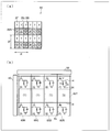
- FIG. 3 is a schematic diagram showing the liquid crystal panel of the present embodiment, (a) is a plan view of a color filter of the liquid crystal panel, and (b) is an equivalent circuit diagram showing a pixel configuration of the TFT substrate.
- columns of colored sub-pixels and columns of transparent sub-pixels are alternately arranged.
- the red sub-pixel, the green sub-pixel, and the blue sub-pixel are repeatedly arranged in this order in the n-th column, and the transparent sub-pixels are continuously arranged in the n + 1-th column.
- the transparent subpixel of the liquid crystal panel overlaps the transmissive region of the first polarizing layer 12 and the transmissive region of the second polarizing layer 22 in plan view, and is a color filter layer. 25 'overlaps with the transparent portion 25T.
- the light transmittance of the liquid crystal panel of this embodiment is 52% as shown in the following equation.
- the light transmittance (52%) of the liquid crystal panel of this embodiment is 3.7 times higher than the light transmittance (14%) of the conventional liquid crystal panel. Therefore, when a liquid crystal panel is used as a liquid crystal panel of a transparent display, the visibility of the transparent display is improved.
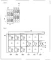
- FIG. 4 is a schematic view showing the liquid crystal panel of the present embodiment, (a) is a plan view of a color filter of the liquid crystal panel, and (b) is an equivalent circuit diagram showing a pixel configuration of the TFT substrate.
- colored sub-pixels and transparent sub-pixels are arranged in a staggered pattern.
- the transparent subpixel of the liquid crystal panel overlaps the transmissive region of the first polarizing layer 12 and the transmissive region of the second polarizing layer 22 in plan view, and is a color filter layer. It overlaps the 25 ′′ transparent part 25T.
- the light transmittance of the liquid crystal panel of this embodiment is 52% as shown in the following equation.
- the light transmittance (52%) of the liquid crystal panel of this embodiment is 3.7 times higher than the light transmittance (14%) of the conventional liquid crystal panel. Therefore, when the liquid crystal panel is used as a liquid crystal panel for a transparent display, the transparency of the display is improved. Further, since the transparent sub-pixels and the colored sub-pixels are arranged in a zigzag pattern, the uniformity of the arrangement pattern of the transparent sub-pixels in plan view is high, and the visibility of the display is further improved.
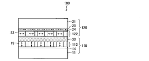
- FIG. 5 is a cross-sectional view of the liquid crystal panel of the present embodiment.
- the liquid crystal panel 100 includes a TFT substrate 110, a counter substrate 120 provided to face the TFT substrate 110, and a liquid crystal layer 30 sandwiched between the TFT substrate 110 and the counter substrate 120. is doing.
- the TFT substrate 110 has a configuration in which the pixel electrode 14 is formed on the counter substrate 120 side of the glass substrate 11 and the first polarizing layer 112 is formed on the pixel electrode 14.
- the counter substrate 120 has a configuration in which the color filter layer 25 is formed on the TFT substrate 110 side of the glass substrate 21, the counter electrode 24 is formed on the color filter layer 25, and the second polarizing layer 122 is formed on the counter electrode 24. have.
- the liquid crystal panel 100 of this embodiment has a so-called in-cell polarizing layer structure.
- the first polarizing layer 112 and the second polarizing layer 122 can be formed by applying an organic dichroic material to the pixel electrode 14 and the counter electrode 24. Further, the first polarizing layer 112 and the second polarizing layer 122 can be formed by selectively not providing a polarizing plate in a region where the pixel electrode 14 is not formed in plan view.
- the liquid crystal panel 100 of the present embodiment can improve contrast as compared with the liquid crystal panel 1 of the first embodiment. Further, by using the in-cell polarizing layer, when the liquid crystal panel 100 is used as a part of the liquid crystal display device, the light source is disposed on the side surface of the glass substrate 11, the light from the light source is guided by the glass substrate 11, It can also be set as the structure inject
- FIG. 1 the structure inject
- FIG. 6 is a cross-sectional view of the organic EL panel of the present embodiment.
- the organic EL panel 200 includes a TFT substrate 210, a counter substrate 220 provided to face the TFT substrate 210, and an organic EL layer 230 sandwiched between the TFT substrate 210 and the counter substrate 220. have.
- the organic EL layer 230 includes a red organic EL layer 230R that emits red light, a green organic EL layer 230G that emits green light, and a blue organic EL layer 230B that emits blue light.
- the organic EL panel 200 of the present embodiment is a display panel that performs display by applying a voltage to the organic EL layers 230R, 230G, and 230B arranged corresponding to the sub-pixels and emitting light of each color.
- the TFT substrate 210 has a configuration in which the pixel electrode 14 is formed on the counter substrate 220 side of the glass substrate 11 and the first polarizing layer 212 is formed on the opposite side of the glass substrate 11 from the counter substrate 220.
- the first polarizing layer 212 includes a first polarizing plate 213 that is a circularly polarizing plate. In a plan view, the polarizing region in which the first polarizing plate 213 is provided, and the first polarizing layer And a transmission region where the plate 213 is not provided.
- the organic EL panel 200 of the present embodiment can suppress external light reflection by providing the TFT substrate 210 with the first polarizing plate 213 that is a circularly polarizing plate.
- the organic EL layers 230R, 230G, and 230B are provided in regions that overlap with the colored sub-pixels in a plan view, and the organic EL layers are formed in regions that overlap the transparent sub-pixels in a plan view Is not provided.
- the organic EL panel 200 has a higher light transmittance than the conventional organic EL panel, and when the organic EL panel 200 is used as an organic EL panel of a transparent display, the visibility of the display is improved. An object can be visually recognized clearly.
- FIG. 7 is a schematic diagram showing the liquid crystal panel of the present embodiment, (a) is a cross-sectional view of the liquid crystal panel, and (b) is a schematic diagram showing the visibility when the liquid crystal panel is used as a transparent display. is there.
- the liquid crystal panel 300 includes a TFT substrate 310, a counter substrate 320 provided to face the TFT substrate 310, and a liquid crystal layer sandwiched between the TFT substrate 310 and the counter substrate 320. 30.
- the counter substrate 320 includes a color filter layer (not shown) formed on the glass substrate 21 on the TFT substrate 310 side, a counter electrode 24 formed on the color filter layer, and a glass substrate 21 on the opposite side to the TFT substrate 310. It has a configuration in which two polarizing layers 322 are formed.
- the second polarizing layer 322 includes a clockwise circularly polarizing plate 323 and a counterclockwise circularly polarizing plate 324, and in a plan view, a polarizing region where the clockwise circularly polarizing plate 323 is provided, and a counterclockwise circularly polarizing plate. Polarizing regions where the plate 324 is provided and transmission regions where the polarizing plate is not provided are alternately arranged.
- the liquid crystal panel 300 of the present embodiment is used as a part of the liquid crystal display device 301, and the liquid crystal display device 301 is passed through a right-eye lens 341 that transmits clockwise circularly polarized light and a left-eye lens 340 that transmits counterclockwise circularly polarized light. Different images can be observed by the left and right eyes. Thereby, 3D (three-dimensional) display can be performed. Also, The light of the transparent line passes through both the right eye lens 341 and the left eye lens 340.
- the liquid crystal panel 300 Since the liquid crystal panel 300 has a transparent line, the light transmittance is high.
- the liquid crystal panel 300 is used as a part of the liquid crystal display device 301, the visibility of the display is improved, so that a 3D image can be displayed as shown in FIG. Can be clearly seen.
- FIG. 8 is a cross-sectional view of the liquid crystal panel 400 of the present embodiment.
- the liquid crystal panel 400 includes a first TFT substrate 440, a first liquid crystal layer 460, a first counter substrate 450, a second TFT substrate 410, a second liquid crystal layer 430, and a second counter substrate 420.
- a first TFT substrate 440 a first liquid crystal layer 460
- a first counter substrate 450 a second TFT substrate 410
- second liquid crystal layer 430 a second liquid crystal layer 430
- a second counter substrate 420 are stacked in this order.
- the first TFT substrate 440 has a configuration in which a pixel electrode 444 is formed on the first counter substrate 450 side of the glass substrate 441 and a first polarizing layer 442 is formed on the opposite side of the glass substrate 441 from the first counter substrate 450. is doing.
- the first counter substrate 450 has a configuration in which a color filter layer 455 is formed on the glass substrate 451 on the first TFT substrate 440 side, and a counter electrode 454 is formed on the color filter layer 455.
- the second TFT substrate 410 has a configuration in which a pixel electrode 414 is formed on the second counter substrate 420 side of the glass substrate 411. Note that the glass substrate 411 is bonded to the glass substrate 451.
- a color filter layer 425 is formed on the second TFT substrate 410 side of the glass substrate 421, a counter electrode 424 is formed on the color filter layer 425, and the glass substrate 421 is opposite to the second counter substrate 420.
- the second polarizing layer 422 is formed on the side.
- the liquid crystal panel 400 is a composite display panel configured by bonding two liquid crystal panels. Two images can be displayed by two liquid crystal panels. Realizing a DFD (Depth-Fused 3-D) 3D display that changes the brightness ratio (brightness ratio) of two images to make the depth position perceived at an arbitrary position between the two liquid crystal panels. can do.
- DFD Depth-Fused 3-D
- the liquid crystal panel 400 of the present embodiment has a colored sub-pixel and a transparent sub-pixel, and the transparent sub-pixel enters the liquid crystal panel 400 from the first TFT substrate 440 side. Light is emitted as it is from the second counter substrate 420 side.
- the light transmittance of the liquid crystal panel 400 of the present embodiment is higher than the light transmittance of the conventional liquid crystal panel, and when the liquid crystal panel 400 is used as a liquid crystal panel of a transparent display, the visibility of the display is improved.
- liquid crystal panel 400 of the present embodiment as a part of the liquid crystal display device, it is possible to display a 3D video and to clearly see an object through the display.
- FIG. 9 is a cross-sectional view of the liquid crystal display device 501 of the present embodiment.
- the liquid crystal display device 501 includes a liquid crystal panel 500 and a light source 540.
- the counter substrate 520 is not provided with a color filter layer.
- the light source 540 emits red light, green light, and blue light alternately toward the liquid crystal panel 500.
- the light source 540 sequentially changes the color of light emitted at a period of 1/60 seconds, for example.
- the liquid crystal display device 501 of the present embodiment is a so-called field sequential type liquid crystal display device. Since the field sequential type liquid crystal display device does not have a color filter layer, the transmittance is improved as compared with a normal liquid crystal display device. However, since a polarizing layer is necessary, the transmittance can be further improved by using the polarizing layers 512 and 522 of the present invention. As a result, the transparency and visibility of the liquid crystal display device can be improved, and the object can be viewed through the liquid crystal display device without applying strong light to the object on the back surface.
- the display panel (the liquid crystal panel 1 and the organic EL panel 200) according to one embodiment of the present invention includes a first substrate (TFT substrate 10) and a second substrate (counter substrate 20) provided to face each other.
- a display panel in which a polarizing layer (first polarizing layer 12, second polarizing layer 22) is provided on at least one of the first substrate and the second substrate, wherein the polarizing layer is provided.
- a polarizing layer first polarizing layer 12, second polarizing layer 22
- the transmission region has a higher light transmittance than the polarization region where the polarizing layer is provided. Therefore, since the transmission region is uniformly arranged in the plan view, the light transmittance of the display panel can be improved uniformly in the plan view. As a result, the object on the back is seen through the display panel. The visibility at the time can be improved.
- the plurality of subpixels are defined in plan view, and the first substrate has pixel electrodes (14) corresponding to the subpixels.
- the pixel electrode may not be provided in a region of the first substrate that overlaps the transmission region in plan view.
- the display panel according to aspect 3 of the present invention further includes a color filter layer (25) in the above aspect 2, and the color filter layer includes a plurality of colored portions (25R ⁇ 25) each transmitting light of different wavelengths. 25G and 25B) and a transparent portion (25T) that transmits all visible light.
- the transparent part transmits light of all wavelengths
- the light transmittance is higher than that of the colored part. Therefore, the light transmittance in the entire display panel can be improved.
- the display panel according to Aspect 4 of the present invention is the display panel according to Aspect 3, wherein the sub-pixel includes a colored sub-pixel (60R, 60G, and 60B) that overlaps the polarizing region and the colored portion in a plan view. And the transparent sub-pixel (60T) that overlaps the transparent region and the transparent portion. In the transparent sub-pixel, light incident from the outside passes through the transparent region and the transparent portion as it is. It may be injected.
- the colored sub-pixel can emit light according to the wavelength transmitted by the colored portion. Further, in the transparent subpixel, the light transmittance can be improved by transmitting light of all wavelengths.
- the display panel according to Aspect 5 of the present invention is the display panel according to Aspect 4, wherein the colored subpixel includes a red subpixel (60R) that emits red light and a green subpixel (60G) that emits green light.
- the blue sub-pixel (60B) that emits blue light is included, and the red sub-pixel, the green sub-pixel, the blue sub-pixel, and the transparent sub-pixel are aligned in a row in plan view. May be arranged.
- transparent sub-pixels with high light transmittance can be uniformly arranged in a plan view.
- the colored sub-pixel columns and the transparent sub-pixel columns may be alternately arranged in a plan view.
- the display panel according to Aspect 7 of the present invention is the display panel according to Aspect 4, wherein the colored subpixels are emitted with a red subpixel that emits red light, a green subpixel that emits green light, and a blue light. Blue subpixels may be included, and the colored subpixels and the transparent subpixels may be arranged in a staggered manner in plan view.
- the polarizing layer provided on the first substrate includes a clockwise circularly polarizing plate (323) and a counterclockwise circularly polarized light.
- the visibility of the display panel can be improved and 3D video can be displayed.
- the polarizing layer may be provided so as to constitute an outer surface of the first substrate.
- the polarizing layer may be provided on the first substrate so as to face the second substrate.
- the above configuration can improve the contrast.
- the light source may be disposed on the side surface of the TFT substrate, and the light from the light source may be guided in the TFT substrate.
- a liquid crystal layer (30) may be provided between the first substrate and the second substrate.
- an organic EL layer may be provided between the first substrate and the second substrate.
- the composite display panel (400) according to aspect 13 of the present invention includes two display panels according to any of the above aspects 1 to 12, and the two display panels may overlap each other.
- the display device (liquid crystal display devices 301 and 501) according to the fourteenth aspect of the present invention may include the display panel according to any of the first to twelfth aspects and a light source.
- the display device may perform field sequential display by sequentially changing the wavelength of light emitted from the light source (540).
- the present invention can be suitably used as a display panel for a transparent display.
- Liquid crystal panel (display panel) 10, 110, 210, 310, 410, 510 TFT substrate (first substrate) 12, 112, 212, 312, 512 First polarizing layer (polarizing layer) 13, 213, 513 First polarizing plate (polarizing plate) 14 Pixel electrode 20, 120, 220, 320, 420, 520 Counter substrate (second substrate) 22, 122, 322, 522 Second polarizing layer (polarizing layer) 23, 523 Second polarizing plate (polarizing plate) 25 Color filter layer 25B, 25G, 25R Colored portion 25T Transparent portion 30 Liquid crystal layer 230 Organic EL layer 60T Transparent subpixel 200 Organic EL panel (display panel) 301, 501 Liquid crystal display device (display device) 323 clockwise circularly polarizing plate 324 counterclockwise circularly polarizing plate 540 light source
Landscapes
- Physics & Mathematics (AREA)
- Nonlinear Science (AREA)
- Mathematical Physics (AREA)
- Chemical & Material Sciences (AREA)
- Crystallography & Structural Chemistry (AREA)
- General Physics & Mathematics (AREA)
- Optics & Photonics (AREA)
- Electroluminescent Light Sources (AREA)
- Liquid Crystal (AREA)
Abstract
表示パネルの光透過率を平面視において均一に向上させた表示パネルを提供する。TFT基板(10)および対向基板(20)のうちの少なくとも何れか一方には、偏光層(12・22)が設けられており、偏光層(12・22)は、平面視において、偏光板(13・23)が設けられている偏光領域と、偏光板(13・23)が設けられていない透過領域とを有しており、透過領域は、平面視において一様に配されている。
Description
本発明は、液晶パネルや有機ELパネルなどの表示パネル及び表示装置に関する。
インテリア・デザイン性やインタラクティブ性の向上などの観点から、ディスプレイ越しに背後にある物体を見ることができる透明ディスプレイが注目されている。透明ディスプレイにおいては、ディスプレイの光透過率の指標である透明性と、ディスプレイ越しに見える物体の明瞭性の指標である視認性とが求められる。
図10は、従来の液晶パネルを示す概略図であり、(a)は従来の液晶パネルの断面図であり、(b)は従来の液晶パネルのカラーフィルターの構成を示す平面図であり、(c)は従来の液晶パネルの透明ディスプレイとして用いた場合の視認性を示す概略図である。
図10の(a)および(b)に示すように、液晶パネル600は、TFT基板610と対向基板620とを備えており、平面視において多数のサブ画素が規定されており、TFT基板610上にはサブ画素に対応して画素電極(図示しない)が設けられ、対向基板620にはサブ画素に対応する位置に着色部を有するカラーフィルター層625が設けられている。また、図10の(a)に示すように、TFT基板610および対向基板620の全面に亘って偏光層612・622が設けられている。
従来の液晶表示装置は、光源と駆動回路と液晶パネルとを備えており、光源から射出される光の、液晶パネルにおける透過率をサブ画素ごとに制御することによってフルカラー表示を行う。
このとき、光源から射出される光のうち、約42%は偏光板を透過する際に減衰し、約33%はカラーフィルターを透過する際に減衰する。表示面全面を白表示する場合であっても、液晶パネル全体の透過率は、光源から射出される光の約10%程度である。
そのため、図10の(c)に示すように、透明ディスプレイ601の表示パネルとして従来の液晶パネル600を用いた場合、偏光板とカラーフィルターによる光損失の大きいため、透明性および視認性が低い。
特許文献1には、カラーフィルターの一部を無色とした半透過型液晶ディスプレイ装置が記載されている。図11は、特許文献1の半透過型液晶ディスプレイ装置のカラーフィルターの構成を示す平面図である。
特許文献1の半透過型液晶ディスプレイ装置は、R,G,Bの3つのカラーサブピクセルおよび無色(W)の第4サブピクセルからなるピクセルを有し、各サブピクセルが反射領域RAと透過領域TAとを有する半透過型液晶ディスプレイ装置である。そして、図11に示すように、カラーフィルター725は、各サブピクセルに対応して、Rf,Gf,Bf、Mfの4つのフィルターセグメントを有している。フィルターセグメントRf・Gf・Bfは、一部に無色サブセグメントWsを有するカラーフィルターセグメントであり、フィルターセグメントMfは無色(透明)のフィルターセグメントである。特許文献1の半透過型液晶ディスプレイ装置は、カラーフィルター725に無色のフィルターセグメントMfを有しているため、反射率を向上させることができる。
また、特許文献2には、電源がオン状態のときでもオフ状態のときでも、所定の模様を表示するために、所定の模様に対応する位置を光反射領域とし、光反射領域における偏光板を削除した液晶表示装置が記載されている。
特許文献1の半透過型液晶ディスプレイ装置は、カラーフィルターの一部を無色としているが、偏光板は従来の液晶表示装置と同様にTFT基板および対向基板の全面に亘って設けられているため、透明ディスプレイとして用いるには液晶パネルの光透過率が不十分である。
また、特許文献2の液晶表示装置は、所定の模様を表示するために所定の模様に合わせて偏光板を除去しているため、液晶パネルの光透過率が平面視において均一ではない。そのため、特許文献2の液晶表示装置は、透明ディスプレイとして用いた場合、ディスプレイ越しに見える物体の境界部分のコントラストが低く、視認性が不十分である。
本発明は、上記の課題に鑑みなされたものであって、その目的は、表示パネルの光透過率を平面視において均一に向上させた表示パネル及びこれを用いた表示装置を提供することにある。
上記の課題を解決するために、本発明の一態様に係る表示パネルは、互いに対向して設けられた第1基板と第2基板とを有しており、上記第1基板および上記第2基板のうちの少なくとも何れか一方には、偏光層が設けられている表示パネルであって、上記偏光層は、平面視において、偏光板が設けられている偏光領域と、上記偏光板が設けられていない透過領域とを有しており、上記透過領域は、平面視において一様に配されていることを特徴とする。
本発明の一態様によれば、表示パネルの光透過率を平面視において均一に向上させることによって、背部にある物体を表示パネル越しに見たときの視認性を向上させることができる。
〔実施形態1〕
以下、本発明の実施の形態について、図1~図4に基づいて詳細に説明する。
以下、本発明の実施の形態について、図1~図4に基づいて詳細に説明する。
以下の説明では、本発明の表示パネルとして液晶パネルを例に挙げて説明する。ただし、これに限ることはなく、本発明は有機ELパネルに適用することもできる。液晶パネルの場合、既存の製造ラインを用いて製造することができるため、製造コストを低減することができる。
図1は、実施形態1の液晶パネルの概略図であり、(a)は液晶パネルの断面図であり、(b)はカラーフィルター層の構成を示す平面図であり、(c)はTFT基板の画素構成を示す等価回路図であり、(d)は液晶パネルを透明ディスプレイとして用いたときの視認性を示す概略図である。
図1の(a)に示すように、液晶パネル1は、TFT基板10(第1基板)と、TFT基板10に対向して設けられた対向基板20(第2基板)と、TFT基板10と対向基板20とに挟持された液晶層30とを有している。
液晶層30としては、ネマティック液晶やポリマーネットワーク型液晶を用いることができる。また、液晶モードとしては、TN(Twisted Nematic)、VA(Vertical Alignment)、ECB(Electrically Controlled Birefringence)、OCB(Optically Compensated Bend)、IPS(In-Plane Switching)等を用いることができる。
液晶パネル1は、平面視において、マトリクス状に規定された複数のサブ画素を有しており、各サブ画素において射出される光を制御されることによって、画像を表示することができる。液晶パネル1のサブ画素は、有色サブ画素と、透明サブ画素とを含んでいる。また、有色サブ画素は、赤色の光を射出する赤色サブ画素と、緑色の光を射出する緑色サブ画素と、青色の光を射出する青色サブ画素とを含んでいる。
透明サブ画素においては、TFT基板10側から液晶パネル1に入射した光が、対向基板20側からそのまま射出される。
なお、本実施形態の液晶パネル1に駆動回路および光源を組み合わせて液晶表示装置としてもよい。この場合、光源としては、従来の液晶表示装置に一般的に用いられるものを採用することができ、または、自然光を光源としてもよい。
<TFT基板>
TFT基板10は、ガラス基板11の対向基板20側に画素電極14が形成され、ガラス基板11の対向基板20とは反対側に第1偏光層12が形成された構成を有している。
TFT基板10は、ガラス基板11の対向基板20側に画素電極14が形成され、ガラス基板11の対向基板20とは反対側に第1偏光層12が形成された構成を有している。
図1の(c)では、液晶パネル1の各サブ画素を破線で図示している。図1の(c)に示すように、ガラス基板11上の、平面視において有色サブ画素60R・60G・60Bに対応する領域には、複数の走査信号線16と複数のデータ信号線15とが設けられており、走査信号線16とデータ信号線15との交差部分にはTFTが設けられている。また、有色サブ画素60R・60G・60Bに重なるように、ガラス基板11上には、画素電極14が設けられており、画素電極14とTFTが電気的に接続されている。画素電極14としては、例えばITOやIZO等の透明導電膜を用いることができる。画素電極14は、後述する対向電極24との間に液晶容量LCと補助容量CSを形成する。
一方で、ガラス基板11上の、平面視において透明サブ画素60Tに重なる領域には、TFTや画素電極14は設けられていない。
また、図1の(a)に示すように、第1偏光層12は、第1偏光板13を含んでおり、平面視において、第1偏光板13が設けられている偏光領域と、第1偏光板13が設けられていない透過領域とを含んでいる。第1偏光板13は、図1の(a)中に示す矢印の方向に透過軸を有している。第1偏光層12において、平面視において有色サブ画素に重なる領域は偏光領域であり、透明サブ画素に重なる領域は透過領域である。また、TFT基板10において、平面視において透過領域に重なる領域には画素電極14は設けられておらず、偏光領域に重なる領域には画素電極14が設けられている。
<対向基板>
対向基板20は、ガラス基板21のTFT基板10側にカラーフィルター層25が形成され、カラーフィルター層25上に対向電極24が形成され、ガラス基板21のTFT基板10とは反対側に第2偏光層22が形成された構成を有している。
対向基板20は、ガラス基板21のTFT基板10側にカラーフィルター層25が形成され、カラーフィルター層25上に対向電極24が形成され、ガラス基板21のTFT基板10とは反対側に第2偏光層22が形成された構成を有している。
図1の(b)に示すように、カラーフィルター層25は、赤色の光を透過する着色部25Rと、緑色の光を透過する着色部25Gと、青色の光を透過する着色部25Bと、全ての可視光をそのまま透過する透明部25Tとを有している。このように、カラーフィルター層25は、それぞれが異なる波長の光を透過させる複数の着色部25R・25G・25Bと透明部25Tとを有しており、着色部25R・25G・25Bと透明部25Tとはこの順に一列に並んでいる。着色部25R・25G・25Bは、TFT基板10の画素電極14に対向するように配置され、透明部25Tは、TFT基板10の画素電極14が設けられていない領域に対向するように配置される。
対向電極24としては、例えばITOやIZO等の透明導電膜を用いることができる。また、カラーフィルター層25としては、カラーレジストインキを用いることができる。カラーレジストインキ用の色材としては、耐光性、耐熱性及び耐溶剤性に優れているために顔料を好適に用いることができる。
図1の(a)に示すように、第2偏光層22は、第2偏光板23を含んでおり、平面視において、第2偏光板23が設けられている偏光領域と、第2偏光板23が設けられていない透過領域とを含んでいる。第2偏光板23は、図1の(a)中に示す矢印の方向に透
過軸を有している。図1の(a)に示すように、第1偏光板13の透過軸と第2偏光板23の偏光軸とは互いに直交している。液晶パネル1は、ノーマリホワイトの液晶パネルである。また、図示はしていないが、ノーマリブラックの液晶パネルであっても良い。
過軸を有している。図1の(a)に示すように、第1偏光板13の透過軸と第2偏光板23の偏光軸とは互いに直交している。液晶パネル1は、ノーマリホワイトの液晶パネルである。また、図示はしていないが、ノーマリブラックの液晶パネルであっても良い。
第2偏光層22において、平面視において有色サブ画素に重なる領域は偏光領域であり、透明サブ画素に重なる領域は透過領域である。
また、カラーフィルター層25の、平面視において有色サブ画素に重なる領域には着色部25R・25G・25Bが設けられており、透明サブ画素に重なる領域には透明部25Tが設けられている。
以上のように、平面視において液晶パネル1の有色サブ画素は、第1偏光層12の偏光領域と第2偏光層22の偏光領域とに重なっており、カラーフィルター層25の着色部25R・25G・25Bに重なっている。
一方で、平面視において液晶パネル1の透明サブ画素は、第1偏光層12の透過領域と第2偏光層22の透過領域とに重なっており、カラーフィルター層25の透明部25Tに重なっている。
これにより、液晶パネル1の透明サブ画素からは、外部から入射した光が、第1偏光層12の透過領域と、液晶層30と、カラーフィルター層25の透明部25Tと、第2偏光層22の透過領域とを透過し、そのまま外部に射出される。
<偏光層の形成方法>
第1偏光層12および第2偏光層22の形成方法としては、以下の方法を採用することができる。
第1偏光層12および第2偏光層22の形成方法としては、以下の方法を採用することができる。
第1に、基材フィルム(ポリビニルアルコール:PVA)にヨウ素や有機染料などの二色性の材料を染色・吸着させ、延伸・配向させることによって、吸収二色性を有する偏光板を形成する。次に、偏光板をガラス基板21・11に貼り合せ、ホイールカッター等を用いて、透過領域に沿って不要な部分の偏光板を除去する。これにより、第1偏光層12および第2偏光層22を形成することができる。
また、第1偏光層12および第2偏光層22の他の形成方法としては、以下の方法を採用することができる。
第1に、ガラス基板21・11上に、液晶性化合物及び二色性色素を含む組成物を形成する。次に、上記組成物において、複屈折性又は偏光性を残したい領域をパターン露光する。パターン露光の手法としてはマスクを用いたコンタクト露光、プロキシ露光、投影露光などでもよいし、レーザーや電子線などを用いてマスクなしに決められた位置にフォーカスして直接描画してもよい。
これにより、TFT基板10または対向基板20に、偏光性を備える偏光板を一様なパターンを有するように形成することができる。
本実施形態の液晶パネル1として、例えば40インチFHD液晶パネルを用いたとすると、ディスプレイサイズは886.8×498.8mmであり、サブ画素のサイズは約115.5μmであり、1画素(各色の有色サブ画素と透明サブ画素)のサイズは約462μmとなる。本実施形態の液晶パネル1のように、TFT基板10または対向基板20の外側に偏光層を設ける場合には、ディスプレイサイズに合わせた大きさで偏光層を貼り合
せ、ホイールカッター等を用いて、透明画素の領域に沿って不要な部分の偏光板を除去する。偏光層の厚みは約0.2mm程度である。
せ、ホイールカッター等を用いて、透明画素の領域に沿って不要な部分の偏光板を除去する。偏光層の厚みは約0.2mm程度である。
液晶パネル1において、平面視において、カラーフィルター層25の透明部25Tが偏光層の透過領域に重なり、カラーフィルター層25の着色部25R・25G・25Bが偏光層の偏光領域に重なることが好ましい。
しかしながら、例えば、液晶パネル1の中央100mm×100mmの部分のみを透過領域としてもよい。
<光透過率>
図2は、カラーフィルター層の構成を示す平面図であり、(a)は従来の液晶パネルのカラーフィルターの平面図であり、(b)は本実施形態の液晶パネルのカラーフィルターの平面図である。
図2は、カラーフィルター層の構成を示す平面図であり、(a)は従来の液晶パネルのカラーフィルターの平面図であり、(b)は本実施形態の液晶パネルのカラーフィルターの平面図である。
図2の(a)に示すカラーフィルター層を有し、TFT基板および対向基板の全面に偏光層が設けられた従来の液晶パネルにおける光透過率は、以下のように求められる。
光透過率=(R着色部の光透過率×R着色部の面積比+G着色部の光透過率×G着色部の面積比+B着色部の光透過率×B着色部の面積比)×偏光層の透過率
一般的には、カラーフィルター層の各色の着色部の光透過率は33%であり、偏光層の光透過率は42%である。
一般的には、カラーフィルター層の各色の着色部の光透過率は33%であり、偏光層の光透過率は42%である。
そのため、従来の液晶パネルの光透過率は、以下の式のとおり、14%となる。
光透過率={(1/3)×(1/3)+(1/3)×(1/3)+(1/3)×(1/3)}×0.42=0.14
これに対して、図2の(b)に示すカラーフィルター層を有し、第1および第2偏光層が透過領域を有する本実施形態の液晶パネルにおける光透過率は、以下のように求められる。
これに対して、図2の(b)に示すカラーフィルター層を有し、第1および第2偏光層が透過領域を有する本実施形態の液晶パネルにおける光透過率は、以下のように求められる。
光透過率=(R着色部の光透過率×R着色部の面積比+G着色部の光透過率×G着色部の面積比+B着色部の光透過率×B着色部の面積比)×偏光層の透過率+透明部(CF)の透過率×透明部(CF)の面積比
本実施形態の液晶パネル1のカラーフィルター層25の、着色部25R・25G・25Bおよび透明部25Tの横幅の合計A’は、従来のカラーフィルター層の着色部の横幅の合計Aと等しく、着色部の縦の長さB’は、従来のカラーフィルター層の着色部の縦の長さBと等しいものとする。
本実施形態の液晶パネル1のカラーフィルター層25の、着色部25R・25G・25Bおよび透明部25Tの横幅の合計A’は、従来のカラーフィルター層の着色部の横幅の合計Aと等しく、着色部の縦の長さB’は、従来のカラーフィルター層の着色部の縦の長さBと等しいものとする。
この場合、透明部(CF)の透過率を90%とすると、本実施形態の液晶パネル1の光透過率は、以下の式のとおり、33%となる。
光透過率={(1/3)×(1/4)+(1/3)×(1/4)+(1/3)×(1/4)}×0.42+0.9×(1/4)=0.33
このように、本実施形態の液晶パネル1の光透過率(33%)は、従来の液晶パネルの光透過率(14%)よりも2.4倍高い。また、本実施形態の液晶パネル1では、偏光層の透過領域およびカラーフィルター層の透明部が平面視において一様に配されている。そのため、液晶パネル1を透明ディスプレイの液晶パネルとして用いた場合、透明ディスプレイの背後にある物体の視認性が向上する。
このように、本実施形態の液晶パネル1の光透過率(33%)は、従来の液晶パネルの光透過率(14%)よりも2.4倍高い。また、本実施形態の液晶パネル1では、偏光層の透過領域およびカラーフィルター層の透明部が平面視において一様に配されている。そのため、液晶パネル1を透明ディスプレイの液晶パネルとして用いた場合、透明ディスプレイの背後にある物体の視認性が向上する。
〔実施形態2〕
本発明の他の実施形態について、図3に基づいて説明すれば、以下のとおりである。なお、説明の便宜上、前記実施形態にて説明した部材と同じ機能を有する部材については、同じ符号を付記し、その説明を省略する。
本発明の他の実施形態について、図3に基づいて説明すれば、以下のとおりである。なお、説明の便宜上、前記実施形態にて説明した部材と同じ機能を有する部材については、同じ符号を付記し、その説明を省略する。
図3は、本実施形態の液晶パネルを示す概略図であり、(a)は液晶パネルのカラーフィルターの平面図であり、(b)はTFT基板の画素構成を示す等価回路図である。
図3の(b)に示すように、本実施形態の液晶パネルは、有色サブ画素の列と透明サブ画素の列とが、交互に配されている。
より具体的には、n列目では、赤色サブ画素と緑色サブ画素と青色サブ画素とがこの順に繰り返し並べられており、n+1列目では、透明サブ画素が連続して並べられている。
また、実施形態1の液晶パネル1と同様に、平面視において液晶パネルの透明サブ画素は、第1偏光層12の透過領域と第2偏光層22の透過領域とに重なっており、カラーフィルター層25’の透明部25Tに重なっている。
本実施形態の液晶パネルの光透過率は、以下の式のとおり、52%となる。
光透過率={(1/3)×(1/6)+(1/3)×(1/6)+(1/3)×(1/6)}×0.42+0.9×(3/6)=0.52
このように、本実施形態の液晶パネルの光透過率(52%)は、従来の液晶パネルの光透過率(14%)よりも3.7倍高い。そのため、液晶パネルを透明ディスプレイの液晶パネルとして用いた場合、透明ディスプレイの視認性する。
このように、本実施形態の液晶パネルの光透過率(52%)は、従来の液晶パネルの光透過率(14%)よりも3.7倍高い。そのため、液晶パネルを透明ディスプレイの液晶パネルとして用いた場合、透明ディスプレイの視認性する。
〔実施形態3〕
本発明の他の実施形態について、図4に基づいて説明すれば、以下のとおりである。なお、説明の便宜上、前記実施形態にて説明した部材と同じ機能を有する部材については、同じ符号を付記し、その説明を省略する。
本発明の他の実施形態について、図4に基づいて説明すれば、以下のとおりである。なお、説明の便宜上、前記実施形態にて説明した部材と同じ機能を有する部材については、同じ符号を付記し、その説明を省略する。
図4は、本実施形態の液晶パネルを示す概略図であり、(a)は液晶パネルのカラーフィルターの平面図であり、(b)はTFT基板の画素構成を示す等価回路図である。
本実施形態の液晶パネルは、有色サブ画素と透明サブ画素とが、千鳥状に配されている。
また、実施形態1の液晶パネル1と同様に、平面視において液晶パネルの透明サブ画素は、第1偏光層12の透過領域と第2偏光層22の透過領域とに重なっており、カラーフィルター層25’’の透明部25Tに重なっている。
本実施形態の液晶パネルの光透過率は、以下の式のとおり、52%となる。
光透過率={(1/3)×(1/6)+(1/3)×(1/6)+(1/3)×(1/6)}×0.42+0.9×(3/6)=0.52
このように、本実施形態の液晶パネルの光透過率(52%)は、従来の液晶パネルの光透過率(14%)よりも3.7倍高い。そのため、液晶パネルを透明ディスプレイの液晶パネルとして用いた場合、ディスプレイの透明性が向上する。また、透明サブ画素と有色サブ画素とを千鳥状に配置しているため、平面視における透明サブ画素の配置パターンの均一性が高く、ディスプレイの視認性がさらに向上する。
このように、本実施形態の液晶パネルの光透過率(52%)は、従来の液晶パネルの光透過率(14%)よりも3.7倍高い。そのため、液晶パネルを透明ディスプレイの液晶パネルとして用いた場合、ディスプレイの透明性が向上する。また、透明サブ画素と有色サブ画素とを千鳥状に配置しているため、平面視における透明サブ画素の配置パターンの均一性が高く、ディスプレイの視認性がさらに向上する。
〔実施形態4〕
本発明の他の実施形態について、図5に基づいて説明すれば、以下のとおりである。なお、説明の便宜上、前記実施形態にて説明した部材と同じ機能を有する部材については、同じ符号を付記し、その説明を省略する。
本発明の他の実施形態について、図5に基づいて説明すれば、以下のとおりである。なお、説明の便宜上、前記実施形態にて説明した部材と同じ機能を有する部材については、同じ符号を付記し、その説明を省略する。
図5は、本実施形態の液晶パネルの断面図である。図5に示すように、液晶パネル100は、TFT基板110と、TFT基板110に対向して設けられた対向基板120と、TFT基板110と対向基板120とに挟持された液晶層30とを有している。
TFT基板110は、ガラス基板11の対向基板120側に画素電極14が形成され、さらに画素電極14上に第1偏光層112が形成された構成を有している。
対向基板120は、ガラス基板21のTFT基板110側にカラーフィルター層25が形成され、カラーフィルター層25上に対向電極24が形成され、対向電極24上に第2偏光層122が形成された構成を有している。
本実施形態の液晶パネル100は、いわゆるインセル偏光層の構造を有している。第1偏光層112および第2偏光層122は、画素電極14および対向電極24に、有機系の二色性物質を塗布することにより形成することができる。また、平面視において画素電極14が形成されていない領域には選択的に偏光板を設けないようにすることによって、第1偏光層112および第2偏光層122を形成することができる。
本実施形態の液晶パネル100は、実施形態1の液晶パネル1に比べ、コントラストを向上させることができる。また、インセル偏光層を用いることで、液晶パネル100を液晶表示装置の一部として用いる場合に、光源をガラス基板11の側面に配置し、光源からの光をガラス基板11により導光し、液晶層30に向けて射出する構成とすることもできる。
〔実施形態5〕
本発明の他の実施形態について、図6に基づいて説明すれば、以下のとおりである。なお、説明の便宜上、前記実施形態にて説明した部材と同じ機能を有する部材については、同じ符号を付記し、その説明を省略する。
本発明の他の実施形態について、図6に基づいて説明すれば、以下のとおりである。なお、説明の便宜上、前記実施形態にて説明した部材と同じ機能を有する部材については、同じ符号を付記し、その説明を省略する。
図6は、本実施形態の有機ELパネルの断面図である。図6に示すように、有機ELパネル200は、TFT基板210と、TFT基板210に対向して設けられた対向基板220と、TFT基板210と対向基板220とに挟持された有機EL層230とを有している。
有機EL層230は、赤色光を射出する赤色有機EL層230Rと、緑色光を射出する緑色有機EL層230Gと、青色光を射出する青色有機EL層230Bとを有している。
本実施形態の有機ELパネル200は、サブ画素に対応して配置された有機EL層230R・230G・230Bに電圧を印加し、各色の光を射出することによって表示を行う表示パネルである。
TFT基板210は、ガラス基板11の対向基板220側に画素電極14が形成され、ガラス基板11の対向基板220とは反対側に第1偏光層212が形成された構成を有している。
図6に示すように、第1偏光層212は、円偏光板である第1偏光板213を含んでおり、平面視において、第1偏光板213が設けられている偏光領域と、第1偏光板213が設けられていない透過領域とを含んでいる。
本実施形態の有機ELパネル200は、TFT基板210に、円偏光板である第1偏光板213を設けることによって、外光反射を抑制することができる。
本実施形態の有機ELパネル200は、平面視において有色サブ画素に重なる領域に、有機EL層230R・230G・230Bが設けられており、平面視において透明サブ画素に重なる領域には、有機EL層は設けられていない。
これにより、有機ELパネル200の透明サブ画素からは、外部から入射した光が、第1偏光層212の透過領域と、有機EL層230とを透過し、そのまま外部に射出される。
そのため、有機ELパネル200は、従来の有機ELパネルに比べて光透過率が高く、有機ELパネル200を透明ディスプレイの有機ELパネルとして用いた場合、ディスプレイの視認性が向上するため、ディスプレイ越しに物体を明瞭に視認することができる。
〔実施形態6〕
本発明の他の実施形態について、図7に基づいて説明すれば、以下のとおりである。なお、説明の便宜上、前記実施形態にて説明した部材と同じ機能を有する部材については、同じ符号を付記し、その説明を省略する。
本発明の他の実施形態について、図7に基づいて説明すれば、以下のとおりである。なお、説明の便宜上、前記実施形態にて説明した部材と同じ機能を有する部材については、同じ符号を付記し、その説明を省略する。
図7は、本実施形態の液晶パネルを示す概略図であり、(a)は液晶パネルの断面図であり、(b)は液晶パネルを透明ディスプレイとして用いたときの視認性を示す概略図である。
図7の(a)に示すように、液晶パネル300は、TFT基板310と、TFT基板310に対向して設けられた対向基板320と、TFT基板310と対向基板320とに挟持された液晶層30とを有している。
対向基板320は、ガラス基板21のTFT基板310側にカラーフィルター層(図示しない)が形成され、カラーフィルター層上に対向電極24が形成され、ガラス基板21のTFT基板310とは反対側に第2偏光層322が形成された構成を有している。
第2偏光層322は、右回り円偏光板323と、左回り円偏光板324とを含んでおり、平面視において、右回り円偏光板323が設けられている偏光領域と、左回り円偏光板324が設けられている偏光領域と、偏光板が設けられていない透過領域とが交互に配されている。
これにより、図7の(b)に示すように、右回りの円偏光が射出される領域(右目用ライン)と、左回りの円偏光が射出される領域(左目用ライン)と、外部からTFT基板310に入射した光がそのまま対向基板320側から外部に射出される領域(透明ライン)とが形成される。
本実施形態の液晶パネル300を液晶表示装置301の一部として用い、右回りの円偏光を透過する右目用レンズ341および左回りの円偏光を透過する左目用レンズ340を介して液晶表示装置301を見る観者に対して、左右の眼によってそれぞれ異なる画像を観察させることができる。これにより、3D(3次元)表示を行うことができる。また、
透明ラインの光は、右目用レンズ341および左目用レンズ340の両方を透過する。
透明ラインの光は、右目用レンズ341および左目用レンズ340の両方を透過する。
液晶パネル300は、透明ラインを有しているため、光透過率が高い。液晶パネル300を液晶表示装置301の一部として用いた場合、ディスプレイの視認性が向上するため、図7の(b)に示すように、3D映像の表示することができるとともに、ディスプレイ越しに物体を明瞭に視認することができる。
〔実施形態7〕
本発明の他の実施形態について、図8に基づいて説明すれば、以下のとおりである。なお、説明の便宜上、前記実施形態にて説明した部材と同じ機能を有する部材については、同じ符号を付記し、その説明を省略する。
本発明の他の実施形態について、図8に基づいて説明すれば、以下のとおりである。なお、説明の便宜上、前記実施形態にて説明した部材と同じ機能を有する部材については、同じ符号を付記し、その説明を省略する。
図8は、本実施形態の液晶パネル400の断面図である。図8に示すように、液晶パネル400は、第1TFT基板440と、第1液晶層460と、第1対向基板450と、第2TFT基板410と、第2液晶層430と第2対向基板420とがこの順に積層されている。
第1TFT基板440は、ガラス基板441の第1対向基板450側に画素電極444が形成され、ガラス基板441の第1対向基板450とは反対側に第1偏光層442が形成された構成を有している。
第1対向基板450は、ガラス基板451の第1TFT基板440側にカラーフィルター層455が形成され、カラーフィルター層455上に対向電極454が形成された構成を有している。
第2TFT基板410は、ガラス基板411の第2対向基板420側に画素電極414が形成された構成を有している。なお、ガラス基板411はガラス基板451に貼り合されている。
第2対向基板420は、ガラス基板421の第2TFT基板410側にカラーフィルター層425が形成され、カラーフィルター層425上に対向電極424が形成され、ガラス基板421の第2対向基板420とは反対側に第2偏光層422が形成された構成を有している。
このように、液晶パネル400は、2つの液晶パネルを貼り合せることによって構成された複合表示パネルである。そして、2つの液晶パネルにより2つの画像を表示することができる。2つの画像の輝度比(明るさの割合)を変化させることによって、2つの液晶パネルの間の任意の位置に奥行き位置を知覚させる、DFD(Depth-Fused 3-D)方式の3Dディスプレイを実現することができる。
さらに、実施形態1と同様に、本実施形態の液晶パネル400は、有色サブ画素と透明サブ画素とを有しており、透明サブ画素からは、第1TFT基板440側から液晶パネル400に入射した光が、第2対向基板420側からそのまま射出される。
そのため、本実施形態の液晶パネル400の光透過率は、従来の液晶パネルの光透過率よりも高く、液晶パネル400を透明ディスプレイの液晶パネルとして用いた場合、ディスプレイの視認性が向上する。
これにより、本実施形態の液晶パネル400を液晶表示装置の一部に用いることによって、3D映像の表示することができるとともに、ディスプレイ越しに物体を明瞭に視認す
ることができる。
ることができる。
〔実施形態8〕
本発明の他の実施形態について、図9に基づいて説明すれば、以下のとおりである。なお、説明の便宜上、前記実施形態にて説明した部材と同じ機能を有する部材については、同じ符号を付記し、その説明を省略する。
本発明の他の実施形態について、図9に基づいて説明すれば、以下のとおりである。なお、説明の便宜上、前記実施形態にて説明した部材と同じ機能を有する部材については、同じ符号を付記し、その説明を省略する。
図9は、本実施形態の液晶表示装置501の断面図である。液晶表示装置501は、液晶パネル500と、光源540とを有している。
本実施形態の液晶パネル500は、対向基板520にカラーフィルター層が設けられていない。
光源540は、液晶パネル500に向けて、赤色光と、緑色光と、青色光とを交互に出射する。光源540は、例えば、1/60秒の周期で出射する光の色を順次変化させる。
本実施形態の液晶表示装置501は、いわゆるフィールドシーケンシャル方式の液晶表示装置である。フィールドシーケンシャル方式の液晶表示装置はカラーフィルター層を有しないため、通常の液晶表示装置よりも透過率が向上する。ただし、偏光層は必要なため本発明の偏光層512・522を用いることによって、さらに透過率を向上させることができる。その結果、液晶表示装置の透視性および視認性を向上することができ、背面の物体に強い光を当てなくても物体を液晶表示装置越しに視認することができる。
〔まとめ〕
本発明の一態様に係る表示パネル(液晶パネル1、有機ELパネル200)は、互いに対向して設けられた第1基板(TFT基板10)と第2基板(対向基板20)とを有しており、上記第1基板および上記第2基板のうちの少なくとも何れか一方には、偏光層(第1偏光層12、第2偏光層22)が設けられている表示パネルであって、上記偏光層は、平面視において、偏光板(第1偏光板13、第2偏光板23)が設けられている偏光領域と、偏光板が設けられていない透過領域とを有しており、上記透過領域は、平面視において一様に配されていることを特徴とする。
本発明の一態様に係る表示パネル(液晶パネル1、有機ELパネル200)は、互いに対向して設けられた第1基板(TFT基板10)と第2基板(対向基板20)とを有しており、上記第1基板および上記第2基板のうちの少なくとも何れか一方には、偏光層(第1偏光層12、第2偏光層22)が設けられている表示パネルであって、上記偏光層は、平面視において、偏光板(第1偏光板13、第2偏光板23)が設けられている偏光領域と、偏光板が設けられていない透過領域とを有しており、上記透過領域は、平面視において一様に配されていることを特徴とする。
透過領域は、偏光層が設けられている偏光領域に比べて光透過率が高い。そのため、平面視において透過領域が一様に配されていることによって、表示パネルの光透過率を平面視において均一に向上させることができ、その結果、背部にある物体を表示パネル越しに見たときの視認性を向上させることができる。
本発明の態様2に係る表示パネルは、上記態様1において、平面視において、複数のサブ画素が規定されており、上記第1基板には、上記サブ画素に対応して、画素電極(14)が設けられており、上記第1基板の、平面視において上記透過領域に重なる領域には、上記画素電極は設けられていない構成であってもよい。
本発明の態様3に係る表示パネルは、上記態様2において、カラーフィルター層(25)をさらに備えており、上記カラーフィルター層は、それぞれが異なる波長の光を透過させる複数の着色部(25R・25G・25B)と、全ての可視光を透過させる透明部(25T)とを備えていてもよい。
透明部は全ての波長の光を透過させるため、着色部に比べて光透過率が高い。そのため、表示パネル全体における光透過率を向上させることができる。
本発明の態様4に係る表示パネルは、上記態様3において、上記サブ画素には、平面視において上記偏光領域および上記着色部と重なっている有色サブ画素(60R・60G・60B)と、平面視において上記透過領域および上記透明部と重なっている透明サブ画素(60T)とが含まれており、上記透明サブ画素においては、外部から入射した光が、上記透過領域および上記透明部を介してそのまま射出されてもよい。
上記の構成により、有色サブ画素においては、着色部が透過させる波長に応じた光を射出することができる。また、透明サブ画素においては、全ての波長の光を透過させることによって、光透過率を向上させることができる。
本発明の態様5に係る表示パネルは、上記態様4において、上記有色サブ画素には、赤色の光を射出する赤色サブ画素(60R)と、緑色の光を射出する緑色サブ画素(60G)と、青色の光を射出する青色サブ画素(60B)とが含まれており、平面視において、上記赤色サブ画素と、緑色サブ画素と、青色サブ画素と、上記透明サブ画素とは、一列に並んで配されていてもよい。
上記の構成により、光透過率の高い透明サブ画素を平面視において一様に配することができる。
本発明の態様6に係る表示パネルは、上記態様4において、平面視において、上記有色サブ画素の列と、上記透明サブ画素の列とが交互に配されていてもよい。
上記の構成により、サブ画素に占める透明サブ画素の割合を大きくすることができる。これにより、光透過率をさらに向上させることができる。
本発明の態様7に係る表示パネルは、上記態様4において、上記有色サブ画素には、赤色の光を射出する赤色サブ画素と、緑色の光を射出する緑色サブ画素と、青色の光を射出する青色サブ画素とが含まれており、平面視において、上記有色サブ画素と、上記透明サブ画素とが千鳥状に配されていてもよい。
上記の構成により、サブ画素に占める透明サブ画素の割合を大きくすることができる。これにより、光透過率をさらに向上させることができる。また、表示パネルの背後にある物体を表示パネル越しに見たときの視認性が向上する。
本発明の態様8に係る表示パネルは、上記態様1~7の何れかにおいて、上記第1基板に設けられた上記偏光層は、右回りの円偏光板(323)と、左回りの円偏光板(324)とを備えており、平面視において、上記右回りの円偏光板が設けられている領域と、上記左回りの円偏光板が設けられている領域と、上記透過領域と、が配されていてもよい。
表示パネルの視認性を向上することができるとともに、3D映像の表示することができる。
本発明の態様9に係る表示パネルは、上記態様1~8の何れかにおいて、上記偏光層は、上記第1基板において、外側の面を構成するように設けられていてもよい。
本発明の態様10に係る表示パネルは、上記態様1~8の何れかにおいて、上記偏光層は、上記第1基板において、上記第2基板に対向して設けられていてもよい。
上記の構成により、コントラストを向上させることができる。光源をTFT基板の側面に配置し、光源からの光をTFT基板内で導光する構成であってもよい。
本発明の態様11に係る表示パネルは、上記態様1~10の何れかにおいて、上記第1基板および上記第2基板の間には、液晶層(30)が設けられていてもよい。
本発明の態様12に係る表示パネルは、上記態様1~10の何れかにおいて、上記第1基板および第2基板の間には、有機EL層(230)が設けられていてもよい。
本発明の態様13に係る複合表示パネル(400)は、上記態様1~12の何れかの表示パネルを2つ備えており、2つの上記表示パネルが、互いに重なっていてもよい。
上記の構成により、DFD方式の3D表示を行うことができる。
本発明の態様14に係る表示装置(液晶表示装置301、501)は、上記態様1~12の何れかの表示パネルと、光源とを備えていてもよい。
本発明の態様15に係る表示装置(液晶表示装置501)は、上記光源(540)が出射する光の波長を順次変化させることにより、フィールドシーケンシャル表示を行ってもよい。
上記の構成により、色再現性の高い表示を行うことができる。また、カラーフィルター層を用いる必要がないため、表示装置の光透過率を向上させることができる。
本発明は上述した各実施形態に限定されるものではなく、請求項に示した範囲で種々の変更が可能であり、異なる実施形態にそれぞれ開示された技術的手段を適宜組み合わせて得られる実施形態についても本発明の技術的範囲に含まれる。さらに、各実施形態にそれぞれ開示された技術的手段を組み合わせることにより、新しい技術的特徴を形成することができる。
本発明は、透明ディスプレイの表示パネルとして、好適に用いることができる。
1、100、300、400、500 液晶パネル(表示パネル)
10、110、210、310、410、510 TFT基板(第1基板)
12、112、212、312、512 第1偏光層(偏光層)
13、213、513 第1偏光板(偏光板)
14 画素電極
20、120、220、320、420、520 対向基板(第2基板)
22、122、322、522 第2偏光層(偏光層)
23、523 第2偏光板(偏光板)
25 カラーフィルター層
25B、25G、25R 着色部
25T 透明部
30 液晶層
230 有機EL層
60T 透明サブ画素
200 有機ELパネル(表示パネル)
301、501 液晶表示装置(表示装置)
323 右回り円偏光板
324 左回り円偏光板
540 光源
10、110、210、310、410、510 TFT基板(第1基板)
12、112、212、312、512 第1偏光層(偏光層)
13、213、513 第1偏光板(偏光板)
14 画素電極
20、120、220、320、420、520 対向基板(第2基板)
22、122、322、522 第2偏光層(偏光層)
23、523 第2偏光板(偏光板)
25 カラーフィルター層
25B、25G、25R 着色部
25T 透明部
30 液晶層
230 有機EL層
60T 透明サブ画素
200 有機ELパネル(表示パネル)
301、501 液晶表示装置(表示装置)
323 右回り円偏光板
324 左回り円偏光板
540 光源
Claims (5)
- 互いに対向して設けられた第1基板と第2基板とを有しており、
上記第1基板および上記第2基板のうちの少なくとも何れか一方には、偏光層が設けられている表示パネルであって、
上記偏光層は、平面視において、偏光板が設けられている偏光領域と、上記偏光板が設けられていない透過領域とを有しており、
上記透過領域は、平面視において一様に配されていることを特徴とする表示パネル。 - 平面視において、複数のサブ画素が規定されており、
上記第1基板には、上記サブ画素に対応して、画素電極が設けられており、
上記第1基板の、平面視において上記透過領域に重なる領域には、上記画素電極は設けられていないことを特徴とする請求項1に記載の表示パネル。 - カラーフィルター層をさらに備えており、
上記カラーフィルター層は、それぞれが異なる波長の光を透過させる複数の着色部と、全ての可視光を透過させる透明部とを備えていることを特徴とする請求項2に記載の表示パネル。 - 上記サブ画素には、平面視において上記偏光領域および上記着色部と重なっている有色サブ画素と、平面視において上記透過領域および上記透明部と重なっている透明サブ画素とが含まれており、
上記透明サブ画素においては、外部から入射した光が、上記透過領域および上記透明部を介してそのまま射出されることを特徴とする請求項3に記載の表示パネル。 - 請求項1~4の何れか1項に記載の表示パネルと、光源とを備えており、
上記光源が出射する光の波長を順次変化させることにより、フィールドシーケンシャル表示を行うことを特徴とする表示装置。
Applications Claiming Priority (2)
| Application Number | Priority Date | Filing Date | Title |
|---|---|---|---|
| JP2013-077901 | 2013-04-03 | ||
| JP2013077901 | 2013-04-03 |
Publications (1)
| Publication Number | Publication Date |
|---|---|
| WO2014162798A1 true WO2014162798A1 (ja) | 2014-10-09 |
Family
ID=51658102
Family Applications (1)
| Application Number | Title | Priority Date | Filing Date |
|---|---|---|---|
| PCT/JP2014/054544 Ceased WO2014162798A1 (ja) | 2013-04-03 | 2014-02-25 | 表示パネル及び表示装置 |
Country Status (1)
| Country | Link |
|---|---|
| WO (1) | WO2014162798A1 (ja) |
Cited By (6)
| Publication number | Priority date | Publication date | Assignee | Title |
|---|---|---|---|---|
| CN104635374A (zh) * | 2015-02-13 | 2015-05-20 | 上海天马微电子有限公司 | 一种显示面板,显示装置及其制造方法 |
| WO2016059847A1 (ja) * | 2014-10-14 | 2016-04-21 | シャープ株式会社 | 表示装置 |
| CN107507855A (zh) * | 2017-09-22 | 2017-12-22 | 京东方科技集团股份有限公司 | 一种显示模组及其制备方法、显示装置 |
| JP2018005111A (ja) * | 2016-07-07 | 2018-01-11 | 株式会社ジャパンディスプレイ | 表示装置 |
| CN107783336A (zh) * | 2016-08-24 | 2018-03-09 | 京东方科技集团股份有限公司 | 透明显示面板及显示装置 |
| JP2023033120A (ja) * | 2021-08-27 | 2023-03-09 | シャープ株式会社 | シースルーウィンドディスプレイおよび液晶ディスプレイ |
Citations (7)
| Publication number | Priority date | Publication date | Assignee | Title |
|---|---|---|---|---|
| JPS58211739A (ja) * | 1982-06-03 | 1983-12-09 | Seiko Epson Corp | 液晶表示体 |
| JPH07104285A (ja) * | 1993-10-08 | 1995-04-21 | Rohm Co Ltd | 液晶表示装置 |
| JP2004295072A (ja) * | 2003-03-27 | 2004-10-21 | Boe Hydis Technology Co Ltd | 液晶表示装置 |
| JP2005039578A (ja) * | 2003-07-16 | 2005-02-10 | Semiconductor Energy Lab Co Ltd | 撮像機能付き表示装置、及び双方向コミュニケーションシステム |
| JP2005309377A (ja) * | 2004-03-23 | 2005-11-04 | Citizen Watch Co Ltd | 液晶表示装置 |
| JP2009157297A (ja) * | 2007-12-28 | 2009-07-16 | Epson Imaging Devices Corp | 液晶表示装置 |
| JP2010170119A (ja) * | 2008-12-25 | 2010-08-05 | Semiconductor Energy Lab Co Ltd | 半導体装置およびその作製方法 |
-
2014
- 2014-02-25 WO PCT/JP2014/054544 patent/WO2014162798A1/ja not_active Ceased
Patent Citations (7)
| Publication number | Priority date | Publication date | Assignee | Title |
|---|---|---|---|---|
| JPS58211739A (ja) * | 1982-06-03 | 1983-12-09 | Seiko Epson Corp | 液晶表示体 |
| JPH07104285A (ja) * | 1993-10-08 | 1995-04-21 | Rohm Co Ltd | 液晶表示装置 |
| JP2004295072A (ja) * | 2003-03-27 | 2004-10-21 | Boe Hydis Technology Co Ltd | 液晶表示装置 |
| JP2005039578A (ja) * | 2003-07-16 | 2005-02-10 | Semiconductor Energy Lab Co Ltd | 撮像機能付き表示装置、及び双方向コミュニケーションシステム |
| JP2005309377A (ja) * | 2004-03-23 | 2005-11-04 | Citizen Watch Co Ltd | 液晶表示装置 |
| JP2009157297A (ja) * | 2007-12-28 | 2009-07-16 | Epson Imaging Devices Corp | 液晶表示装置 |
| JP2010170119A (ja) * | 2008-12-25 | 2010-08-05 | Semiconductor Energy Lab Co Ltd | 半導体装置およびその作製方法 |
Cited By (12)
| Publication number | Priority date | Publication date | Assignee | Title |
|---|---|---|---|---|
| WO2016059847A1 (ja) * | 2014-10-14 | 2016-04-21 | シャープ株式会社 | 表示装置 |
| CN104635374A (zh) * | 2015-02-13 | 2015-05-20 | 上海天马微电子有限公司 | 一种显示面板,显示装置及其制造方法 |
| US9658485B2 (en) | 2015-02-13 | 2017-05-23 | Shanghai Tianma Micro-electronics Co., Ltd. | Display panel, a display device, and fabrication method thereof |
| CN104635374B (zh) * | 2015-02-13 | 2017-09-01 | 上海天马微电子有限公司 | 一种显示面板,显示装置及其制造方法 |
| JP2018005111A (ja) * | 2016-07-07 | 2018-01-11 | 株式会社ジャパンディスプレイ | 表示装置 |
| CN107783336A (zh) * | 2016-08-24 | 2018-03-09 | 京东方科技集团股份有限公司 | 透明显示面板及显示装置 |
| US10606117B2 (en) | 2016-08-24 | 2020-03-31 | Boe Technology Group Co., Ltd. | Transparent display panels and display devices |
| CN107507855A (zh) * | 2017-09-22 | 2017-12-22 | 京东方科技集团股份有限公司 | 一种显示模组及其制备方法、显示装置 |
| JP2023033120A (ja) * | 2021-08-27 | 2023-03-09 | シャープ株式会社 | シースルーウィンドディスプレイおよび液晶ディスプレイ |
| CN115881048A (zh) * | 2021-08-27 | 2023-03-31 | 夏普株式会社 | 透视显示器及液晶显示器 |
| US11874577B2 (en) | 2021-08-27 | 2024-01-16 | Sharp Kabushiki Kaisha | See-through window display and liquid crystal display |
| CN115881048B (zh) * | 2021-08-27 | 2025-09-30 | 夏普株式会社 | 透视显示器 |
Similar Documents
| Publication | Publication Date | Title |
|---|---|---|
| JP3187306B2 (ja) | 透過型液晶表示装置 | |
| US9268168B2 (en) | Liquid crystal display device and method of fabricating the same | |
| US8120718B2 (en) | Parallax barrier device for viewing three-dimensional images, method for fabricating the same and display apparatus including a parallax barrier device | |
| CN108027528A (zh) | 显示设备和驱动方法 | |
| JP5568409B2 (ja) | 立体表示装置 | |
| WO2014162798A1 (ja) | 表示パネル及び表示装置 | |
| KR102380640B1 (ko) | 액정캡슐을 포함하는 액정표시장치 | |
| JP6169482B2 (ja) | 液晶装置、電子機器及び液晶装置製造方法 | |
| KR101425611B1 (ko) | 패턴드 리타더 방식의 입체영상 표시장치 및 그 제조 방법 | |
| WO2013069387A1 (ja) | 表示装置およびその駆動方法と製造方法 | |
| WO2015146462A1 (ja) | タッチパネル付き表示装置 | |
| JPH10153771A (ja) | 液晶表示装置 | |
| WO2013099794A1 (ja) | 立体表示装置 | |
| KR101314402B1 (ko) | 표시 장치 | |
| US9983445B2 (en) | Liquid crystal lens panel and display device including liquid crystal lens panel | |
| WO2013065580A1 (ja) | 表示装置 | |
| US9354453B2 (en) | Stereoscopic image display device and method for manufacturing the same | |
| JP2009157301A (ja) | 電気光学装置 | |
| CN118244527A (zh) | 3d影像显示用有源延迟器和显示装置 | |
| KR101266218B1 (ko) | 입체 영상 표시 장치 | |
| CN102722033B (zh) | 三维显示装置及三维显示系统 | |
| JP5176993B2 (ja) | 電気光学装置及び電子機器 | |
| US12169291B2 (en) | Stereoscopic image display device and a method of manufacturing the same | |
| KR101949388B1 (ko) | 3d 영상 표시장치 | |
| US20120212815A1 (en) | Stereoscopic image display device |
Legal Events
| Date | Code | Title | Description |
|---|---|---|---|
| 121 | Ep: the epo has been informed by wipo that ep was designated in this application |
Ref document number: 14779895 Country of ref document: EP Kind code of ref document: A1 |
|
| NENP | Non-entry into the national phase |
Ref country code: DE |
|
| 122 | Ep: pct application non-entry in european phase |
Ref document number: 14779895 Country of ref document: EP Kind code of ref document: A1 |
|
| NENP | Non-entry into the national phase |
Ref country code: JP |