WO2014162776A1 - 発光素子パッケージの製造方法及び発光素子パッケージ - Google Patents
発光素子パッケージの製造方法及び発光素子パッケージ Download PDFInfo
- Publication number
- WO2014162776A1 WO2014162776A1 PCT/JP2014/053132 JP2014053132W WO2014162776A1 WO 2014162776 A1 WO2014162776 A1 WO 2014162776A1 JP 2014053132 W JP2014053132 W JP 2014053132W WO 2014162776 A1 WO2014162776 A1 WO 2014162776A1
- Authority
- WO
- WIPO (PCT)
- Prior art keywords
- liquid repellent
- substrate
- repellent film
- opening
- light emitting
- Prior art date
- Legal status (The legal status is an assumption and is not a legal conclusion. Google has not performed a legal analysis and makes no representation as to the accuracy of the status listed.)
- Ceased
Links
Images




Classifications
-
- H—ELECTRICITY
- H10—SEMICONDUCTOR DEVICES; ELECTRIC SOLID-STATE DEVICES NOT OTHERWISE PROVIDED FOR
- H10W—GENERIC PACKAGES, INTERCONNECTIONS, CONNECTORS OR OTHER CONSTRUCTIONAL DETAILS OF DEVICES COVERED BY CLASS H10
- H10W90/00—Package configurations
-
- H—ELECTRICITY
- H10—SEMICONDUCTOR DEVICES; ELECTRIC SOLID-STATE DEVICES NOT OTHERWISE PROVIDED FOR
- H10H—INORGANIC LIGHT-EMITTING SEMICONDUCTOR DEVICES HAVING POTENTIAL BARRIERS
- H10H20/00—Individual inorganic light-emitting semiconductor devices having potential barriers, e.g. light-emitting diodes [LED]
- H10H20/80—Constructional details
- H10H20/85—Packages
- H10H20/852—Encapsulations
- H10H20/853—Encapsulations characterised by their shape
-
- H—ELECTRICITY
- H10—SEMICONDUCTOR DEVICES; ELECTRIC SOLID-STATE DEVICES NOT OTHERWISE PROVIDED FOR
- H10W—GENERIC PACKAGES, INTERCONNECTIONS, CONNECTORS OR OTHER CONSTRUCTIONAL DETAILS OF DEVICES COVERED BY CLASS H10
- H10W74/00—Encapsulations, e.g. protective coatings
-
- H—ELECTRICITY
- H10—SEMICONDUCTOR DEVICES; ELECTRIC SOLID-STATE DEVICES NOT OTHERWISE PROVIDED FOR
- H10W—GENERIC PACKAGES, INTERCONNECTIONS, CONNECTORS OR OTHER CONSTRUCTIONAL DETAILS OF DEVICES COVERED BY CLASS H10
- H10W90/00—Package configurations
- H10W90/701—Package configurations characterised by the relative positions of pads or connectors relative to package parts
- H10W90/751—Package configurations characterised by the relative positions of pads or connectors relative to package parts of bond wires
- H10W90/753—Package configurations characterised by the relative positions of pads or connectors relative to package parts of bond wires between laterally-adjacent chips
-
- H—ELECTRICITY
- H10—SEMICONDUCTOR DEVICES; ELECTRIC SOLID-STATE DEVICES NOT OTHERWISE PROVIDED FOR
- H10W—GENERIC PACKAGES, INTERCONNECTIONS, CONNECTORS OR OTHER CONSTRUCTIONAL DETAILS OF DEVICES COVERED BY CLASS H10
- H10W90/00—Package configurations
- H10W90/701—Package configurations characterised by the relative positions of pads or connectors relative to package parts
- H10W90/751—Package configurations characterised by the relative positions of pads or connectors relative to package parts of bond wires
- H10W90/754—Package configurations characterised by the relative positions of pads or connectors relative to package parts of bond wires between a chip and a stacked insulating package substrate, interposer or RDL
Definitions
- the present invention relates to a method for manufacturing a light emitting device package and a light emitting device package.
- a light-emitting element such as a light-emitting diode (LED) is used as a light source for a backlight of a liquid crystal display device or a lighting device.
- LED light-emitting diode
- an LED package is used.
- the LED package is configured by sealing an LED mounted on a substrate with a sealing resin.
- a sealing resin is formed on the substrate, first, a liquid repellent film is patterned in an annular shape surrounding the periphery of the LED mounted on the substrate. Thereafter, a sealing resin is formed on the substrate by coating or the like inside the annular shape.
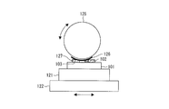
- FIG. 12 is a diagram showing a state of the conventional liquid repellent film printing apparatus when not printing.
- FIG. 13 is a diagram illustrating a state during printing by a conventional liquid repellent film printing apparatus.
- a printing plate 126 is disposed on the surface of the printing machine roller unit 125 of the printing system 120, and the liquid repellent ink 127 adheres on the printing plate 126 so as to be the same as the annular shape of the liquid repellent film. is doing.
- An alignment stage 121 is disposed on the printing machine stage unit 122 of the printing system 120, and the substrate 101 is disposed on the alignment stage 121.
- Electrodes 102 and 103 are patterned on the surface of the substrate 101. One of the electrodes 102 and 103 is an anode electrode, and the other is a cathode electrode.
- the printing press roller unit 125 rotates in conjunction with the movement of the printing press stage unit 122. Thereby, the liquid repellent ink 127 attached to the printing plate 126 is transferred to the printing surface of the substrate 101. Thus, an annular liquid repellent film is formed on the substrate 101.
- Patent Document 2 describes a method of forming an annular liquid repellent film by applying a liquid repellent resin in an annular shape around a region where an LED chip is mounted on a substrate. .
- Japanese Patent Publication Japanese Patent Laid-Open No. 2012-15320 (published on January 19, 2012)” Japanese Patent Publication “Japanese Patent Laid-Open No. 2012-104594 (published May 31, 2012)”
- the printing press roller unit 125 and the printing plate 126 are replaced, due to individual differences between the printing press roller unit 125 and the printing plate 126, they are formed on the substrate 101 before and after replacement of the printing press roller unit 125 and the printing plate 126.
- the annular shape of the liquid repellent film may also change.
- the shape of the sealing resin formed thereafter also changes, and the chromaticity of the completed LED package also varies. As a result, there is a problem that the yield decreases.
- the present invention has been made to solve the above-described problems, and its purpose is to suppress the amount of liquid repellent ink used, and to stably and quickly open a liquid repellent film on which the liquid repellent ink is solidified.
- the portion By forming the portion, the variation in the shape of the sealing resin is suppressed, the manufacturing time is shortened, and the yield reduction is suppressed.
- a method for manufacturing a light-emitting element package includes a substrate, a light-emitting element disposed on the substrate, and a sealing resin that seals the light-emitting element.
- a method for manufacturing a light emitting device package having a spraying step of spraying liquid repellent ink on the substrate, and solidifying the liquid repellent ink sprayed on the substrate to form a liquid repellent film on the substrate A solidification step and a mask provided with an opening having a shape corresponding to a light emitting element formation region that surrounds a position on the substrate on which the light emitting element is to be disposed are placed on the liquid repellent film, and plasma
- a liquid repellent film removing step for removing the liquid repellent film on the light emitting element formation region by performing a treatment, and the light emitting element on the substrate from which the liquid repellent film has been removed in the liquid repellent film removing step Forming the sealing resin in the formation region of And a degree.
- the amount of liquid-repellent ink is suppressed, and an opening is stably formed in a short time and in a liquid-repellent film on which the liquid-repellent ink is solidified.
- the variation in shape can be suppressed, and the production time can be shortened and the yield can be prevented from being lowered.
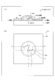
- FIG. 2 is a diagram showing an LED package 10 according to an embodiment of the present invention, (a) is a cross-sectional view of the LED package 10 according to an embodiment of the present invention, and (b) is an embodiment of the present invention. It is a top view (plan view) of the LED package 10 according to the embodiment. In FIG. 2, the LED chip formation area in which LED chip is formed among the LED packages 10 is shown.
- An LED package (light emitting element package) 10 includes a pair of electrodes 2 and 3, two LED chips (light emitting elements) 4, a sealing resin 5 for sealing the LED chip 4, and a sealing. And a liquid repellent film 20 provided on the outer edge of the resin 5.
- the LED package 10 may be arranged on the substrate 1 as a pair of the electrodes 2 and 3, the LED chip 4, and the sealing resin 5, or a plurality of them may be arranged.
- a plurality of LED packages 10 are arranged on the substrate 1 as a pair of electrodes 2 and 3, LED chips 4, and sealing resin 5.
- the substrate 1 is a wiring substrate (interposer substrate) on which the LED chip 4 is mounted.
- the substrate 1 is a ceramic substrate.
- substrate 1 is not limited to a ceramic board
- One of the electrodes 2 and 3 is an anode electrode, and the other is a cathode electrode.
- the electrodes 2 and 3 are wirings (wiring patterns) for the LED chip 4 formed on the substrate 1. Although not shown, a part of the electrodes 2 and 3 (wiring pattern) is insulated from others by an insulating member such as glass.
- the LED chip 4 is a light emitting element in the LED package 10.
- the LED chip 4 is disposed between the electrode 2 and the electrode 3.
- the LED chip 4 is connected to the electrodes 2 and 3 by wires 7. Thereby, the board
- two LED chips 4 are installed at the center of the LED formation region of the substrate 1.
- the number of LED chips 4 installed in the LED formation region is not particularly limited and may be one or more.
- the emission color of the LED chip 4 is not particularly limited.
- the LED chip 4 is used as a light emitting element, but other light emitting elements such as a semiconductor laser and an organic EL element can also be used.
- the sealing resin 5 seals LED chip 4 and wire 7.
- the sealing resin 5 is, for example, a silicone resin (silicone resin, epoxy-modified silicone resin, alkyd-modified silicone resin, acrylic-modified silicone resin, polyester-modified silicone resin, phenylsilicone resin), epoxy resin, acrylic resin, methacrylic resin, urethane resin. It is formed from transparent resin. More specifically, as the sealing resin 5, SCR-1011 (A / B), SCR-1012 (A / B), SCR-1016 (A / B), KER-2500 (A / B) manufactured by Shin-Etsu Chemical Co., Ltd. B), KER-2600 (A / B), ASP-1010 (A / B), ASP-1020 (A / B) (all trade names), SE 1700 Clear (trade names) manufactured by Dow Corning be able to.
- silicone resin silicone resin
- the sealing resin 5 is preferably transparent, but is not necessarily transparent if it can transmit most of the light emission of the LED chip 4 and the light emission of the phosphor in the sealing resin 5.
- the transparent resin constituting the sealing resin 5 is preferably as the transmittance is high, and the refractive index is desirably small in the refractive index difference from the outside (air). Further, as in the present embodiment, when the surface of the sealing resin 5 is spherical (the sealing resin 5 is a dome shape), reflection at the interface between the sealing resin 5 and the outside can be reduced. Therefore, the light extraction efficiency of the LED package 10 can be increased.
- the liquid repellent film 20 is disposed on the substrate 1 and the electrodes 2 and 3.
- the liquid repellent film 20 is patterned so as to surround the LED chip 4 and is in contact with the outer peripheral portion of the sealing resin 5.
- the liquid repellent film 20 has an opening 20a in the LED chip formation region.
- the LED chip formation region can also be expressed as a region in the opening 20a of the liquid repellent film 20.
- the LED chip 4 is disposed in the opening 20 a of the liquid repellent film 20.
- the liquid repellent film 20 is disposed on the substrate 1 and the electrodes 2 and 3, and an opening 20 a that surrounds the LED chip 4 in a circular shape is formed.
- most of the sealing resin 5 is disposed in the opening 20 a of the liquid repellent film 20, that is, in the formation region of the LED chip 4, and a part of the sealing resin 5 is the liquid repellent film 20. Riding on top.
- the liquid repellent film 20 is formed by patterning from a transparent liquid repellent ink.
- the transparent liquid repellent ink has a property of lower wettability to the sealing resin 5 than the substrate 1. That is, the liquid repellent film 20 has a relatively low affinity for the sealing resin 5.
- the liquid repellent film 20 plays a role of controlling the shape of the sealing resin 5 by utilizing the affinity for the sealing resin 5 different from that of the substrate 1. Thereby, the dispersion
- planar shape of the opening 20a of the liquid repellent film 20 is not particularly limited, but is preferably circular as in the present embodiment.
- the surface shape of the sealing resin 5 can be surely made spherical.
- the usage-amount of sealing resin 5 can be minimized and cost can be reduced.
- FIG. 1 is a diagram illustrating a manufacturing process of the LED package 10, where (a) represents a spraying process, (b) represents a solidification process, (c) represents an etching process, and (d) represents a mounting process. Represents a sealing resin forming step. 1 is provided with a plurality of LED chips 4 and a patterned liquid repellent film 20 in the plane of the substrate 1.
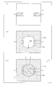
- FIG. 3A and 3B are plan views of the substrate in each manufacturing process of the LED package 10.
- FIG. 3A shows the plane of the LED chip forming region of the substrate to be put into the spraying process
- FIG. 3B shows the LED chip formation of the substrate after the etching process.
- (C) represents the plane of the LED chip forming area of the manufactured LED package 10. In FIG. 3, only the vicinity of the area where the LED chip 4 is arranged in the substrate 1 is shown.
- the LED package 10 is mainly manufactured through a liquid repellent ink spraying process, a solidifying process, an etching process ((liquid repellent film removing process), a mounting process, and a sealing resin forming process.
- the spray device 30 includes a table 31 on which the substrate 1 is placed, a spray unit 32 arranged above the table 31, a support column 33 that supports the spray unit 32, and a liquid repellent ink 21 on the spray unit 32. And a pressurized tank part 34 for supplying the liquid.
- the spray device 30 includes a control unit (not shown) that controls driving of the table 31 and the spray unit 32.
- the table 31 is movable in the Y axis direction which is a horizontal direction as shown in FIG. On the table 31, the substrate 1 on which the liquid repellent ink 21 is sprayed is placed.
- the spray unit 32 sprays the liquid repellent ink 21 toward the substrate 1 placed on the table 31.
- the spray unit 32 is an air spray spray gun.
- the spray unit 32 is spaced apart from the table 31 and the substrate 1 placed on the table 31, and is disposed above the substrate 1 placed on the table 31.
- the spray unit 32 is movable in the X-axis direction and the Z-axis direction, which are directions orthogonal to the Y-axis direction.
- the X axis direction and the Y axis direction are horizontal and orthogonal to each other.
- the Z-axis direction is the vertical direction.
- the spray unit 32 is supported so as to be movable in the X-axis direction and the Z-axis direction.
- a nozzle that is a spray hole for the liquid repellent ink 21 is provided at the tip of the spray unit 32.
- the liquid repellent ink 21 may be a transparent ink containing a liquid repellent material such as a fluorine polymer-containing ink (for example, “Marvel Coat (trade name)” manufactured by Hiejiang Chemical Co., Ltd.).
- the liquid repellent ink 21 is not particularly limited as long as the wettability with respect to the sealing resin 5 is lower than that of the substrate 1.
- the pressurized tank section 34 is for supplying the liquid repellent ink 21 to the spray unit 32 in order for the spray unit 32 to spray the liquid repellent ink 21.
- the liquid repellent ink 21 is supplied from the pressurizing tank unit 34 to the spray unit 32 through the tube (extruded by air pressure).
- the spray amount (liquid repellent ink consumption) of the liquid repellent ink 21 sprayed from the spray unit 32 of the spray unit 32, and the coating film Uniformity can be controlled.
- the hydraulic pressure P1 is a pressure applied to the liquid repellent ink 21 supplied to the spray unit 22 for spraying. Increasing the fluid pressure P1 increases the amount of liquid repellent ink used and increases the coating film density.
- the arrangement position of the pressurized tank unit 34 is not particularly limited as long as the liquid repellent ink 21 can be supplied to the spray unit 32.
- the pressurized tank unit 34 is arranged as an individual unit and connected to the spray unit 32 by a tube. Then, the liquid repellent ink 21 is supplied from the pressure tank unit 34 to the spray unit 32 through the tube.
- the spray unit 32 controls the atomizing air pressure P2, which is the pressure of air (gas) supplied to the spray unit 32 in order to atomize from the nozzle of the spray unit 32 and spray the liquid repellent ink 21, the spray unit 32 It is possible to control the spray particle size and coating film uniformity of the sprayed liquid repellent ink 21. Since the spray diffusion angle from the nozzle of the spray unit 32 is determined by the nozzle shape, the spray range on the substrate 1 is determined by the height of the substrate 1 and the nozzle. Therefore, if the distance of the nozzle of the spray unit 32 from the substrate 1 is long, the spray range is widened, but the uniformity of the coating film density is relatively lowered.
- P2 is the pressure of air (gas) supplied to the spray unit 32 in order to atomize from the nozzle of the spray unit 32 and spray the liquid repellent ink 21.
- the substrate 1 is first prepared. Then, an operator or apparatus places the substrate 1 on the table 31. A plurality of patterned electrodes 2 and 3 are arranged in advance on the surface of the substrate 1 placed on the table 31. As shown in FIG. 3A, the electrodes 2 and 3 are arranged in the vicinity of the formation region of the LED chip 4.
- a plurality of pin openings 1 a are formed near the end of the substrate 1.
- the pin opening 1a is for use in a plasma processing step to be described later.
- the table 31 moves in the XY axis direction, and the substrate 1 is moved to the spray start position.
- the support column 33 adjusts the position of the spray unit 32 in the Z-axis direction so that the distance between the spray unit 32 and the substrate 1 in the Z-axis direction becomes an optimum distance.
- the distance between the nozzle of the spray unit 32 and the substrate 1 is about 140 mm or more and 160 mm or less.
- the liquid repellent ink is then transferred into the spray unit 32 from the pressurized tank portion 34 to which the hydraulic pressure P1 is applied. 21 and an atomizing air pressure P2 is applied to the spray unit 32 from an external atomizing air pressurizing mechanism (not shown).
- the hydraulic pressure P1 is 0.03 MPa or more and 0.04 MPa or less
- the atomizing air pressure P2 is about 0.04 MPa or more and 0.06 MPa or less.
- the liquid repellent ink 21 is sprayed toward the substrate 1 from the nozzles of the spray unit 32.
- the table 31 moves in the Y-axis direction, and the spray unit 32 moves in the X-axis direction.
- the substrate 1 is moved relative to the spray unit 32.
- the moving speed of the table 31 is about 90 (mm / s) or more and 110 (mm / s) or less.
- the pressurizing tank unit 34, the external atomizing air pressurizing mechanism, and the table 31 operate. And the spraying of the liquid repellent ink 21 is finished.
- the liquid repellent ink 21 is provided on the substrate 1 so as to cover the electrodes 2 and 3.
- the liquid repellent ink 21 is sprayed directly from the spray unit 32 onto the substrate 1 and the liquid repellent ink 21 is provided on the substrate 1, so that the liquid repellent ink can be sprayed when necessary.
- the spraying device 30 does not require consumable parts such as the printing machine roller unit 125 and the printing plate 126 of the printing system 120 shown in FIGS. For this reason, the increase in cost accompanying consumable parts replacement
- the liquid repellent ink 21 is provided on the substrate 1 by spraying, the liquid repellent ink 21 can be provided on the substrate 1 thinly over a wide range. That is, the liquid repellent ink can be provided on the substrate 1 in a short time.
- the moving speed of the table 31 is set to 90 (mm / s) to 110 (mm / s), and the hydraulic pressure P1 is set to 0.03 MPa to 0.03 MPa.
- the atomizing air pressure P2 is set to 0.04 MPa or more and 0.06 MPa or less by setting the atomizing air pressure P2 to 04 MPa or less, it is possible to reduce the film thickness variation in the substrate of the liquid repellent ink 21 sprayed on the substrate 1. For this reason, the variation in the substrate of the size of the opening 20a (described later) of the liquid repellent film 20 formed by solidifying the liquid repellent ink 21 on the substrate 1 can be suppressed.
- liquid repellent ink 21 is sprayed, and the sprayed liquid repellent ink 21 is solidified to form the liquid repellent film 22 on the substrate 1. It can be formed into a film.
- the liquid repellent ink 21 on the substrate 1 can be solidified by evaporating the solvent of the liquid repellent ink 21, and the method is not limited to the method in which heat is applied by the oven 40, but other methods. May be.
- the substrate 1 on which the liquid repellent film 22 is formed by solidifying the liquid repellent ink 21 in the solidifying process is transported to the etching process.
- the plasma apparatus 50 includes a chamber 51 that is a work room for performing plasma processing, and a stage 52 and an electrode unit 54 disposed in the chamber 51.
- the plasma apparatus 50 includes a control unit (not shown) that controls driving of the stage 52 and the electrode unit 54.
- the stage 52 is for placing the set plate 53 on which the substrate 1 is set and fixed.
- the stage 52 is disposed near the bottom surface in the chamber 51.
- the electrode unit 54 is an electrode that discharges plasma.
- the electrode portion 54 is spaced apart from the substrate 1 disposed on the stage 52 via the set plate 53 and is disposed above the stage 52.
- the substrate 1 on which the liquid repellent film 22 is formed and the set plate 53 on which the mask 60 is set are placed on the stage 52.
- the mask 60 is a mask for patterning openings in the liquid repellent film 22.
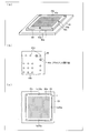
- FIG. 4A and 4B are views showing a substrate, a set plate and a mask used in the etching process.
- FIG. 4A is a perspective view showing a state where the substrate and the mask are set on the set plate
- FIG. 4B is a set on the set plate. It is a figure showing the made board
- the substrate 1 having the liquid repellent film 22 formed thereon is placed on the set plate 53.
- a mask 60 for forming a pattern is placed on the liquid repellent film 22 so as to be in direct contact with the liquid repellent film 22 on the substrate 1.
- a pin 53 a for fixing the substrate 1 and the mask 60 is disposed on the surface of the set plate 53 on which the substrate 1 is disposed.
- the pin 53a has a shape corresponding to the pin opening 1a provided in the substrate 1 (see (c) in FIG. 1 and (c) in FIG. 4) and the pin opening 60a provided in the mask 60.
- the substrate 1 and the mask 60 are fixed by being inserted into the respective pin openings 1a and 60a.
- three pins 53a are arranged so as to be positioned at substantially central portions of three sides of the four sides of the substrate 1 and the mask 60 to be placed.
- the number and position of the pins 53a are not particularly limited, and one or a plurality of pins 53a may be arranged so that the substrate 1 and the mask 60 can be fixed. What is necessary is just to be arranged in the position which can fix each.
- the substrate 1 is provided with a pin opening 1a into which the pin 53a is inserted at a position corresponding to the pin 53a of the set plate 53 (the same position in plan view) when placed on the set plate 53.
- the pin opening 1 a is disposed so as to be positioned at substantially the center of each of the three sides of the four sides of the substrate 1.
- the mask 60 has a pin opening 60a for inserting the pin 53a of the set plate 53, a pattern opening 60b for patterning the opening 20a of the liquid repellent film 20, and an alignment check.
- An alignment opening 60c is provided.
- the mask 60 may be provided with a pattern confirmation opening 60 d for confirming the pattern of the opening 20 a of the liquid repellent film 20.
- the mask 60 is preferably made of metal in order to suppress deterioration due to plasma processing as much as possible.
- the mask 60 is made of stainless steel (SUS).
- the pin opening 60 a is provided at a position corresponding to the pin 53 a of the set plate 53 when the mask 60 is placed on the set plate 53 together with the substrate 1. That is, when the mask 60 is placed on the substrate 1 set on the set plate 53 via the liquid repellent film 22, the pin opening 60a is the same as the pin 53a and the pin opening 1a in plan view. It is arranged on the mask 60 so as to be positioned. In the present embodiment, the pin opening 60 a is disposed so as to be positioned at substantially the center of each of the three sides of the four sides of the mask 60.
- the pattern opening 60 b is provided on the entire surface of the mask 60 at a position and shape corresponding to the opening 20 a of the liquid repellent film 20 to be formed on the substrate 1. That is, the shape of the pattern opening 60b is a shape corresponding to the LED chip formation region.
- the mask 60 is made of a material constituting the mask 60. That is, the mask 60 has a structure for shielding plasma between adjacent pattern openings 60b.
- pattern confirmation openings 60d having the same shape as the pattern openings 60b.
- the pattern confirmation opening 60 d is for forming the opening 20 c of the dummy liquid repellent film 20 formed along the four sides of the substrate 1.
- the opening 20c of the liquid repellent film 20 is formed for confirming the pattern and shape of the opening 20a of the liquid repellent film 20.
- Alignment openings 60 c are arranged in the vicinity of the four corners of the mask 60.
- the alignment opening 60 c is a position adjustment opening with respect to the substrate 1.
- the opening 60 c for alignment is arranged at a position of the mask 60 that overlaps with an alignment mark made of gold or the like provided on the substrate 1 when the mask 60 is arranged on the substrate 1.
- the substrate 1 on which the liquid repellent film 22 is arranged is placed on the set plate 53.
- a mask 60 is placed on the substrate 1 so as to be in direct contact with the liquid repellent film 22.
- the pin 53a of the set plate is inserted into the pin opening 1a of the substrate 1 and the pin opening 60a of the mask 60.
- the substrate 1 and the mask 60 are fixed to the set plate 53.
- the set plate 53 is installed on the stage 52 of the plasma apparatus 50. Note that only the set plate 53 may be placed on the stage 52 first, and then the substrate 1 and the mask 60 may be placed on the set plate 53 in order.
- argon (Ar) gas is sent into the chamber 51 through the pipe 55, and plasma is generated from the electrode portion 54.
- Ar argon
- the plasma device 50 dry-etches the liquid repellent film 22 in the LED chip forming region, which is an unnecessary part of the liquid repellent film 22, or in the opening 20c forming region of the dummy liquid repellent film 20. .
- the liquid repellent film 20 in which the opening 20a and the opening 20c are patterned can be obtained on the substrate 1.
- the structure for shielding plasma is used, so that the adjacent openings formed in the liquid repellent film 20 on the substrate 1 as shown in FIG.
- the substrate 1 is not exposed and is covered with the liquid repellent film 20.
- the mask 60 is placed on the liquid repellent film 22 and subjected to plasma treatment, thereby removing the liquid repellent film 22 in the LED chip formation region on the substrate 1 to form the liquid repellent film in which the opening 20a is formed. 20 is obtained on the substrate 1. For this reason, the liquid repellent film 20 in which the opening 20a is formed can be provided on the substrate 1 in a short time.
- the mask 60 is used in the etching process, the pattern shape changes before and after the replacement of the printing machine roller unit 125 and the printing plate 126, which are consumables, like the printing system 120 shown in FIGS. Can be prevented. As a result, yield reduction can be suppressed.
- the opening 20a can be formed in a shorter time than the case where the liquid repellent film is formed by coating as in Patent Document 2, for example. Variations in the shape of 20a can be suppressed.
- the pattern opening 60b and the pattern confirmation opening 60d of the mask 60 are formed in the mask 60 so as to have a smaller area than the openings 20a and 20c of the liquid repellent film 20. Is preferred.
- FIG. 5 is a cross-sectional view of the substrate 1, the liquid repellent film 22 (liquid repellent film 20), and the mask 60 before and after etching.
- FIG. 5A is a cross section of the substrate 1, the liquid repellent film 22, and the mask 60 before etching.
- b) represents a cross section of the substrate 1, the liquid repellent film 20, and the mask 60 after etching.
- the mask 60 is directly placed on the liquid repellent film 22 when dry etching is performed by the plasma apparatus 50. Then, as shown in FIG. 5B, the unnecessary liquid repellent film 22 under the opening 60b of the mask 60 is removed. At this time, the liquid repellent film 22 is over-etched.
- the diameter 60R (see FIGS. 5A and 5B) of the opening 60b of the mask 60 is set to the diameter 20R of the opening 20a of the liquid repellent film 20 (FIG. 5B and FIG. 3B). (See below). Thereby, even if the opening 20a is over-etched, the opening 20a having a desired area can be obtained.
- the mounting process will be described with reference to FIG.
- the substrate 1 on which the opening 20a of the liquid repellent film 20 is formed in the etching process is then transferred to the mounting process.
- the LED chip 4 is disposed in the opening 20a of the liquid repellent film 20, that is, on the substrate 1 and in the LED chip formation region.
- the LED chip 4 and the electrodes 2 and 3 are connected by a wire 7. Thereby, the LED chip 4 is mounted in the LED chip forming region on the substrate 1.
- the sealing resin forming step will be described with reference to FIGS. 1E and 3C.
- the substrate 1 on which the LED chip 4 is mounted is then transferred to a sealing resin forming process.
- an ink for sealing resin that becomes the sealing resin 5 is formed so as to cover the LED chip 4 in the opening 20a of the liquid repellent film 20, that is, on the substrate 1 and in the LED chip forming region. Apply.
- the ink for sealing resin is solidified by applying heat or the like.
- the LED chip 4 is covered in the opening 20a of the liquid repellent film 20, that is, on the substrate 1 and in the LED chip formation region.
- the sealing resin 5 is formed.
- the region in the opening 20 a of the liquid repellent film 20 (the LED chip forming region on the substrate 1) is a highly wettable (lyophilic) region with respect to the sealing resin ink that becomes the sealing resin 5.
- the liquid repellent film 20 is a region having low wettability (liquid repellency) with respect to the sealing resin ink to be the sealing resin 5. For this reason, when the sealing resin ink to be the sealing resin 5 is applied in the opening 20a of the liquid repellent film 20, the sealing resin ink spreads on the substrate 1 in the opening 20a and opens. It contacts the inner side surface (inner wall surface) of the liquid repellent film 20 in 20a.
- the LED package 10 is completed.
- the LED package 10 may be completed by cutting the substrate 1 into individual pieces so as to include a necessary number of LED chips 4.
- a liquid repellent film (liquid repellent pattern) is formed in an annular shape (ring shape) along the LED chip formation region.
- annular shape ring shape
- the area of the surface of the annular liquid repellent film 20 is small, and the sealing resin ink may overflow from the annular liquid repellent film.
- the liquid repellent film 20 is disposed between adjacent LED chip forming regions. That is, the LED chip forming area is covered with the liquid repellent film 20, and the substrate 1 is not exposed.
- the sealing resin that becomes the sealing resin 5 reliably on the inner surface or surface in the opening 20a of the liquid repellent film 20
- the spreading of the ink for use can be stopped (dammed).
- formation failure of the sealing resin 5 can be suppressed.
- the application amount of the ink for sealing resin used as the sealing resin 5, that is, the degree of freedom of the size of the sealing resin 5 can be increased.
- the liquid repellent ink 21 was deposited on the substrate 1 on which the electrodes 2 and 3 were formed by spraying the liquid repellent ink 21 from the spray unit 32 using the spray device 30. .
- the distance in the Z-axis direction from the nozzle of the spray unit 32 to the substrate 1 was 150 mm.
- the moving speed of the table 31 when spraying the liquid repellent ink 21 was 100 (mm / sec).
- the hydraulic pressure P1 of the spray unit 32 was 0.035 MPa, and the atomizing air pressure P2 was 0.5 MPa.
- heat in the range of 120 ° C. ⁇ 5 ° C. is applied to the substrate 1 on which the liquid repellent ink 21 is disposed within a range of 45 minutes to 60 minutes by the oven 40,
- the solvent of the liquid repellent ink 21 was solidified by vaporization, and a liquid repellent film 22 was formed on the substrate 1.
- the mask 60 is directly placed on the liquid repellent film 22 formed on the substrate 1, and dry etching is performed using the Ar gas using the plasma apparatus 50, thereby forming the liquid repellent film 22.
- the unnecessary part of was removed.
- the average value of the diameter 60R of the opening 60b for the pattern of the mask 60 used at this time was about 1907.54 ⁇ m.
- the RF of the plasma apparatus 50 was 250 W, and the plasma processing time for the liquid repellent film 22 on the substrate 1 was 30 seconds. Thus, the substrate 1 on which the liquid repellent film 20 having the opening 20a was formed was obtained.
- Comparative Examples 1 and 2 only the hydraulic pressure P1 of the spray unit 32 was changed from the condition that the liquid repellent film 20 was formed on the substrate 1.
- the hydraulic pressure P1 of the spray unit 32 was set to 0.03 MPa.
- the hydraulic pressure P1 of the spray unit 32 was 0.04 MPa.
- Comparative Examples 3 and 4 only the atomizing air pressure P2 was changed from the condition in which the liquid repellent film 20 was formed on the substrate 1.
- the atomizing air pressure P2 was set to 0.25 MPa.
- the atomizing air pressure P2 was set to 0.75 MPa.
- Comparative Examples 5 and 6 only the spray height was changed from the condition in which the liquid repellent film 20 was formed on the substrate 1.
- the spray height was 123 mm.
- the spray height was 177 mm.
- Comparative Examples 7 and 8 only the plasma processing time by the plasma apparatus 50 was changed from the condition that the liquid repellent film 20 was formed on the substrate 1.
- the plasma treatment time was 45 seconds.
- the plasma processing time was 60 seconds.
- Comparative Examples 9 and 10 only the RF intensity by the plasma apparatus 50 was changed from the condition that the liquid repellent film 20 was formed on the substrate 1.
- the RF of the plasma apparatus 50 was 225 W.
- the RF of the plasma apparatus 50 was 275 W.
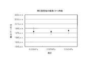
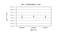
- FIG. 6 is a diagram showing the inner diameter of the opening of the liquid repellent film for each hydraulic pressure P1 setting.
- the horizontal axis represents the liquid pressure P1
- the “liquid repellent pattern inner diameter” on the vertical axis represents the diameter of the opening formed in the liquid repellent film.
- the maximum diameter of the opening formed in the liquid repellent film on the substrate according to Comparative Example 1 was 1994.26 ⁇ m, and the minimum was 1964.44 ⁇ m. It was.
- the maximum diameter of the opening 20a formed in the liquid repellent film 22 on the substrate 1 was 1981.35 ⁇ m and the minimum was 1960.26 ⁇ m.
- the maximum diameter of the opening formed in the liquid repellent film on the substrate according to Comparative Example 2 was 1989.21 ⁇ m, and the minimum was 1965.05 ⁇ m. It was.
- the hydraulic pressure P1 of the spray unit 32 is in the range of 0.03 MPa or more and 0.040 MPa or less, variation in the size of the opening 20 a of the liquid repellent film 20 in the surface of the substrate 1 is sufficiently suppressed. It was found that the size of the opening 20a can be made uniform. This is presumably because the variation in the thickness of the liquid repellent film 20 on the substrate 1 was suppressed and made uniform.
- the diameter (diameter 20R) of the opening 20a of the liquid repellent film 20 on the substrate 1 prepared in this example and the diameters of the openings of the liquid repellent film on the substrates of Comparative Examples 3 and 4 were measured. .
- FIG. 7 is a diagram showing the inner diameter of the opening of the liquid repellent film for each setting of the atomizing air pressure P2.
- the horizontal axis represents the atomizing air pressure P2
- the “liquid repellent pattern inner diameter” on the vertical axis represents the diameter of the opening formed in the liquid repellent film.
- the maximum diameter of the opening formed in the liquid repellent film on the substrate according to Comparative Example 3 was 1998.94 ⁇ m, and the minimum was 1957.19 ⁇ m. It was.
- the maximum diameter of the opening 20a formed in the liquid repellent film 22 on the substrate 1 was 1997.14 ⁇ m and the minimum was 192.63 ⁇ m.
- the maximum diameter of the opening formed in the liquid repellent film on the substrate according to Comparative Example 4 was 1994.69 ⁇ m, and the minimum was 1956.48 ⁇ m. It was.
- the diameter (diameter 20R) of the opening 20a of the liquid repellent film 20 on the substrate 1 prepared in this example and the diameter of the opening of the liquid repellent film on each of the comparative examples 5 and 6 were measured. .
- FIG. 8 is a diagram showing the inner diameter of the opening of the liquid repellent film for each spray height setting.
- the horizontal axis represents the spray height
- the “liquid repellent pattern inner diameter” on the vertical axis represents the diameter of the opening formed in the liquid repellent film.
- the maximum diameter of the opening formed in the liquid repellent film on the substrate according to Comparative Example 5 was 2014.69 ⁇ m and the minimum was 1946.0 ⁇ m, as indicated by the horizontal axis “123 mm” in FIG.
- the maximum diameter of the opening 20 a formed in the liquid repellent film 22 on the substrate 1 was 1997.14 ⁇ m and the minimum was 192.63 ⁇ m.
- the maximum diameter of the opening formed in the liquid repellent film on the substrate according to Comparative Example 6 was 2016.37 ⁇ m and the minimum was 1971.21 ⁇ m.
- the average value of the diameter 20R of the opening 20a shown in FIG. 8 was compared with the average value of the diameter 60R of the opening 60b for the pattern of the mask 60.
- FIG. 9 is a diagram comparing the average value of the diameter of the opening 20a of the liquid repellent film 20 with the average value of the diameter 60R of the opening 60b for the pattern of the mask 60.
- the average value of the diameter 60R of the pattern opening 60b of the mask 60 was 1907.54 ⁇ m.
- the average value of the diameters 20R of the openings 20a of the liquid repellent film 20 was 1974.40 ⁇ m as shown in the column “Liquid repellent pattern inner diameter” in FIG.
- the opening 20a of the liquid repellent film 20 is actually formed to be approximately 66 ⁇ m larger than the pattern opening 60b of the mask 60. That is, it was found that in the plasma treatment process, the liquid repellent film 20 was over-etched to form the opening 20a.
- the diameter of the opening 20a of the liquid repellent film 20 on the substrate 1 was compared with the diameter of the opening of the liquid repellent film on each of the substrates in Comparative Examples 3 and 4.
- FIG. 10 is a diagram showing the relationship between the plasma processing time and the inner diameter of the opening of the liquid repellent film.
- the horizontal axis represents the plasma time (second)
- the “liquid repellent pattern inner diameter” on the vertical axis represents the diameter ( ⁇ m) of the opening formed in the liquid repellent film.
- the horizontal axis “30” (seconds) in FIG. 10 represents the diameter of the opening 20a formed in the liquid repellent film 22 on the substrate 1.
- the maximum diameter was 2006.4 ⁇ m and the minimum was 1958.25 ⁇ m. .
- the horizontal axis “45” (seconds) in FIG. 10 represents the diameter of the opening formed in the liquid repellent film on the substrate according to Comparative Example 7, the maximum being 2019.45 ⁇ m and the minimum being 1968.81 ⁇ m. .
- the horizontal axis “60” (seconds) in FIG. 10 represents the diameter of the opening formed in the liquid repellent film on the substrate according to Comparative Example 8, the maximum being 2036.97 ⁇ m and the minimum being 1961.66 ⁇ m. .
- the diameter of the opening 20a of the liquid repellent film 20 on the substrate 1 was compared with the diameter of the opening of the liquid repellent film on each of the substrates in Comparative Examples 9 and 10.
- FIG. 11 is a diagram showing the relationship between the RF during the plasma treatment and the inner diameter of the opening of the liquid repellent film.
- the horizontal axis represents RF output intensity (W)
- the vertical axis “liquid repellent pattern inner diameter” represents the diameter of the opening formed in the liquid repellent film.
- the horizontal axis “225” (W) in FIG. 11 represents the diameter of the opening formed in the liquid repellent film on the substrate according to Comparative Example 9, the maximum being 2025.0 ⁇ m and the minimum being 1950.33 ⁇ m. .
- the horizontal axis “250” (W) in FIG. 11 represents the diameter of the opening 20a formed in the liquid repellent film 22 on the substrate 1, and the maximum diameter was 2006.4 ⁇ m and the minimum was 1958.25 ⁇ m. .
- the horizontal axis “275” (seconds) in FIG. 11 represents the diameter of the opening formed in the liquid repellent film on the substrate according to Comparative Example 10, and the maximum was 2049.96 ⁇ m and the minimum was 1965.76 ⁇ m. .
- the plasma processing step by setting the RF of plasma to 250 W, variation in the size of the opening 20a of the liquid repellent film 20 in the surface of the substrate 1 is suppressed, and the size of the opening 20a is uniform. I found out that This is considered to be because variation in overetching was suppressed by controlling the plasma processing output.
- a method for manufacturing a light-emitting element package according to aspect 1 of the present invention is a method for manufacturing a light-emitting element package that includes a substrate, a light-emitting element disposed on the substrate, and a sealing resin that seals the light-emitting element.
- the light emitting element includes a spraying step of spraying the liquid repellent ink on the substrate, a solidifying step of solidifying the liquid repellent ink sprayed on the substrate and forming a liquid repellent film on the substrate, and the light emitting element.
- the liquid repellent ink may be sprayed only when the liquid repellent ink is provided on the substrate, and the liquid repellent ink is not sprayed when it is not necessary to provide the liquid repellent ink on the substrate.
- the amount used can be suppressed.
- the liquid repellent ink since the liquid repellent ink is provided on the substrate by spraying, the liquid repellent ink can be provided on the substrate thinly in a wide range. Since the sprayed liquid repellent ink is solidified to form a liquid repellent film on the substrate, the liquid repellent film can be formed on the substrate in a shorter time than before. Further, the mask is placed on the liquid-repellent film and plasma treatment is performed to remove the liquid-repellent film on the light-emitting element formation region.
- the variation in the shape of the opening of the liquid repellent film can be suppressed.
- the said sealing resin is formed in the formation area of the said light emitting element on the said board
- the area of the opening of the mask is such that the liquid repellent film on the light emitting element forming region is removed in the liquid repellent film removing step. It is smaller than the area of the opening of the liquid repellent film formed.
- the liquid repellent film having a desired size is formed.
- the opening can be obtained.
- the mask is provided with a plurality of openings having a shape corresponding to each of the adjacent light emitting element formation regions.
- the plurality of openings are shielded from plasma discharged during the plasma treatment, and in the liquid repellent film removing step, the liquid repellent film covers between the adjacent light emitting element formation regions. Further, the liquid repellent film on the light emitting element formation region is removed.
- the liquid-repellent film covers the adjacent light emitting element forming regions on the substrate, it is possible to suppress the formation failure of the sealing resin formed in the light emitting element forming region. .
- the method for manufacturing a light emitting device package according to aspect 4 of the present invention is the above-described aspect 1 to 3, wherein in the spraying step, the nozzle of the spray unit that sprays the liquid repellent ink from the nozzle onto the substrate, the substrate, The distance applied is 140 mm or more and 160 mm or less, and the pressure applied to the liquid repellent ink supplied to the spray unit for spraying is 0.03 MPa or more and 0.04 MPa or less, and the liquid repellent ink is atomized from the nozzle.
- the pressure of the gas supplied to the liquid repellent ink in the spray unit is 0.04 MPa or more and 0.06 MPa or less.
- the light emitting element package according to the fifth aspect of the present invention is manufactured by the method for manufacturing a semiconductor element package according to the first to fourth aspects. With the above structure, a light-emitting element package with reduced manufacturing time and reduced yield can be obtained.
- the present invention can be used for a method for manufacturing a light emitting element and a light emitting element.
Landscapes
- Led Device Packages (AREA)
Abstract
基板(1)上に撥液インク(21)を噴霧し、当該撥液インク固化後の撥液膜(22)にマスク(60)を配し、プラズマ処理し、LED形成領域上に開口部(20a)が形成された撥液膜(20)を得る。上記開口部に封止樹脂(5)を形成する。これにより、撥液インクの使用量を抑制し、固化後の撥液膜に短時間でかつ安定して開口部を形成し、封止樹脂の形状のバラつきを抑え、製造時間の短縮及び歩留低下を防止する。
Description
本発明は発光素子パッケージの製造方法及び発光素子パッケージに関する。
液晶表示装置のバックライトや照明装置等の光源として、発光ダイオード(LED)等の発光素子が使用されている。LEDが光源として使用される際、LEDパッケージが用いられている。
LEDパッケージは、基板に実装されたLEDが、封止樹脂によって封止されることで構成されている。封止樹脂が基板に形成される際、まず、基板に実装されたLEDの周囲を囲む円環状に撥液膜がパターン形成される。その後、基板上であって、円環状の内部に封止樹脂が塗布等によって形成される。
この円環状の撥液膜をパターン形成する方法として、従来から、特許文献1に記載されているようにフレキソ印刷が用いられている。
図12は従来の撥液膜の印刷装置の非印刷時の状態を表す図である。図13は従来の撥液膜の印刷装置の印刷時の状態を表す図である。
印刷システム120の印刷機ローラ部125の表面には、印刷版126が配されており、印刷版126上に、撥液膜の円環状の形状と同一となるように、撥液インク127が付着している。印刷システム120の印刷機ステージ部122上にはアライメントステージ121が配されており、そのアライメントステージ121上に基板101が配されている。基板101の表面には電極102・103がパターン形成されている。なお、電極102・103のうち一方がアノード電極、他方がカソード電極である。
図13に示すように、撥液インク127の転写時には、印刷機ローラ部125は、印刷機ステージ部122の動きに連動して回転する。これにより、印刷版126に付着した撥液インク127が基板101の印刷面に転写される。このように、基板101上に円環状の撥液膜が形成される。
また、特許文献2には、基板上のLEDチップが実装される領域の周囲に、撥液性樹脂を円環状に塗布することで、円環状の撥液膜を形成する方法が記載されている。
しかしながら、図12、図13に示したフレキソ印刷では、転写する撥液インク127が乾燥しないように、印刷版126に撥液インク127を常時滴下しておく必要がある。このため、無駄な撥液インク127の使用量が多くなるという問題がある。
さらに、印刷機ローラ部125や印刷版126の交換に際し、印刷機ローラ部125や印刷版126の個体差から、印刷機ローラ部125や印刷版126の交換前後で、基板101上に形成される撥液膜の円環状の形状も変わってしまう場合がある。この撥液膜の円環状の形状が変わると、その後形成される封止樹脂の形状も変わるため、完成したLEDパッケージの色度もバラつくことになる。この結果、歩留が低下するという問題がある。
特許文献2のように、基板に撥液性樹脂を円環状に塗布していると、円環状の形状が完成するまで時間がかかり、タクトを低下させるという問題がある。
加えて、円環状の外縁や内縁の側面等、塗布によってパターン形成された円環状の形状にバラつきが生じる。この結果、特許文献2の技術も、封止樹脂の形状のバラつき及び完成したLEDパッケージの色度のバラつきを招来し、歩留が低下するという問題がある。
本発明は、上記課題を解決するためになされたもので、その目的は、撥液インクの使用量を抑制し、当該撥液インクが固化した撥液膜に、短時間でかつ安定して開口部を形成することで、封止樹脂の形状のバラつきを抑え、製造時間の短縮及び歩留低下の抑制を行うことである。
上記の課題を解決するために、本発明の一態様に係る発光素子パッケージの製造方法は、基板と、上記基板上に配された発光素子と、当該発光素子を封止する封止樹脂とを有する発光素子パッケージの製造方法であって、上記基板上に、撥液インクを噴霧する噴霧工程と、上記基板上に噴霧された撥液インクを固化し、基板上に撥液膜を成膜する固化工程と、上記発光素子が配されるべき上記基板上の位置を囲む領域である発光素子の形成領域と対応する形状の開口部が設けられたマスクを上記撥液膜に載置し、プラズマ処理を行うことで、上記発光素子の形成領域上の上記撥液膜を除去する撥液膜除去工程と、上記撥液膜除去工程で上記撥液膜が除去された上記基板上の上記発光素子の形成領域に、上記封止樹脂を形成する封止樹脂形成工程とを有する。
本発明の一態様によれば、撥液インクの使用量を抑制し、当該撥液インクが固化した撥液膜に、短時間でかつ安定して開口部を形成することで、封止樹脂の形状のバラつきを抑え、製造時間の短縮及び歩留低下を防止することができるという効果を奏する。
〔実施形態1〕
以下、本発明の実施の形態について、詳細に説明する。
以下、本発明の実施の形態について、詳細に説明する。
(発光素子パッケージ)
図2は本発明の一実施形態に係るLEDパッケージ10を表す図であり、(a)は本発明の一実施形態に係るLEDパッケージ10の断面図であり、(b)は本発明の一実施形態に係るLEDパッケージ10の上面図(平面図)である。図2では、LEDパッケージ10のうち、LEDチップが形成されるLEDチップ形成領域を示している。
図2は本発明の一実施形態に係るLEDパッケージ10を表す図であり、(a)は本発明の一実施形態に係るLEDパッケージ10の断面図であり、(b)は本発明の一実施形態に係るLEDパッケージ10の上面図(平面図)である。図2では、LEDパッケージ10のうち、LEDチップが形成されるLEDチップ形成領域を示している。
LEDパッケージ(発光素子パッケージ)10は、基板1上に、一対の電極2・3と、2個のLEDチップ(発光素子)4と、LEDチップ4を封止する封止樹脂5と、封止樹脂5の外縁に設けられた撥液膜20とを備えている。
LEDパッケージ10は、電極2・3と、LEDチップ4と、封止樹脂5とが一対として、基板1上に一つ配されていてもよいし、複数配されていてもよい。本実施の形態では、LEDパッケージ10は、電極2・3と、LEDチップ4と、封止樹脂5とが一対として、基板1上に複数配されているものとする。
基板1は、LEDチップ4が実装される配線基板(インターポーザ基板)である。一例として基板1はセラミック基板である。なお、基板1はセラミック基板に限定されるものではなく、他に、ガラス基板、プリント基板、TAB基板(ポリイミド製のテープ状フレキシブル回路基板)などを用いることができる。電極2・3の一方がアノード電極、他方がカソード電極である。電極2・3は、基板1上に形成された、LEDチップ4用の配線(配線パターン)である。なお、図示しないが、電極2・3(配線パターン)の一部は、ガラス等の絶縁部材によって、他から絶縁されている。
LEDチップ4は、LEDパッケージ10における発光素子である。LEDチップ4は、電極2と電極3との間に配置されている。LEDチップ4は、ワイヤ7によって、電極2・3と接続されている。これにより、基板1とLEDチップ4とが、電気的および機械的に接続される。
なお、図2においては、2個のLEDチップ4が基板1のLED形成領域の中央部に設置されている。LED形成領域内のLEDチップ4の設置数は、特に限定されるものではなく、1個以上であればよい。また、LEDチップ4の発光色も特に限定されるものではない。また、本実施形態では、LEDチップ4を発光素子としているが、半導体レーザ、有機EL素子等の他の発光素子を用いることも可能である。
封止樹脂5は、LEDチップ4およびワイヤ7を封止する。封止樹脂5は、例えば、シリコーン樹脂(シリコーン樹脂,エポキシ変性シリコーン樹脂,アルキッド変性シリコーン樹脂,アクリル変性シリコーン樹脂,ポリエステル変性シリコーン樹脂,フェニルシリコーン樹脂)、エポキシ樹脂、アクリル樹脂、メタクリル樹脂、ウレタン樹脂などの透明樹脂から形成されている。より具体的には、封止樹脂5として、信越化学社製のSCR-1011(A/B),SCR-1012(A/B),SCR-1016(A/B),KER-2500(A/B),KER-2600(A/B),ASP-1010(A/B),ASP-1020(A/B)(いずれも商品名)、ダウコーニング社製のSE 1700 Clear(商品名)を用いることができる。
封止樹脂5は、透明であることが好ましいが、LEDチップ4の発光、および、封止樹脂5中の蛍光体の発光の大部分を透過することができれば、必ずしも透明である必要はない。
なお、封止樹脂5を構成する透明樹脂は、透過率が高いほど好ましく、屈折率は外部(空気)との屈折率差が小さいことが望ましい。また、本実施の形態のように、封止樹脂5の表面が球面形状(封止樹脂5がドーム状)であれば、封止樹脂5と外部との界面における反射を低減することができる。従って、LEDパッケージ10の光取り出し効率を高めることができる。
撥液膜20は、基板1上及び電極2・3上に配されている。撥液膜20は、LEDチップ4を包囲するようにパターン形成されていると共に、封止樹脂5の外周部に接している。撥液膜20には、LEDチップ形成領域に開口部20aが設けられている。換言すると、LEDチップ形成領域は、撥液膜20の開口部20a内の領域であると表現することもできる。撥液膜20の開口部20a内にLEDチップ4が配されている。具体的には、本実施の形態では、撥液膜20は、基板1上及び電極2・3上に配されており、LEDチップ4の周囲を円状に囲む開口部20aが形成されている。また、本実施の形態では、封止樹脂5の大部分は、撥液膜20の開口部20a内、すなわちLEDチップ4の形成領域に配され、封止樹脂5の一部が撥液膜20上に乗り上げている。
詳細は後述するが、撥液膜20は、透明の撥液インクからパターン形成されたものである。透明の撥液インクは、基板1よりも封止樹脂5に対する濡れ性が低い性質を有する。すなわち、撥液膜20は、封止樹脂5に対する親和性が相対的に低くなる。撥液膜20は、このような基板1とは異なる封止樹脂5に対する親和性を利用して、封止樹脂5の形状を制御する役割を果たす。これにより、封止樹脂5の形状のばらつきが抑制されている。
また、撥液膜20の開口部20aの平面形状は、特に限定されるものではないが、本実施形態のように円状であることが好ましい。これにより、封止樹脂5の表面形状を、確実に球面とすることができる。また、封止樹脂5の使用量を最小にすることができ、コストを低下させることができる。
(LEDパッケージ10の製造方法)
次に、図1、図3~図5を用いて、LEDパッケージ10の製造方法について説明する。
次に、図1、図3~図5を用いて、LEDパッケージ10の製造方法について説明する。
図1は、LEDパッケージ10の製造工程を表す図であり、(a)は噴霧工程を表し(b)は固化工程を表し(c)エッチング工程を表し(d)は実装工程を表し(e)は封止樹脂形成工程を表している。なお、図1に示す基板1には、LEDチップ4やパターン形成された撥液膜20が基板1の面内に複数配される。
図3はLEDパッケージ10の各製造工程における基板の平面図であり(a)は噴霧工程に投入される基板のLEDチップ形成領域の平面を表し(b)はエッチング工程後の基板のLEDチップ形成領域の平面を表し(c)は製造されたLEDパッケージ10のLEDチップ形成領域の平面を表している。なお、図3では、基板1のうち、LEDチップ4が配される領域近傍のみを表している。
LEDパッケージ10は、主に、撥液インクの噴霧工程、固化工程、エッチング工程((撥液膜除去工程)、実装工程、封止樹脂形成工程を経て、製造される。以下、順に説明する。
〈撥液インクの噴霧工程〉
まず、図1の(a)及び図3の(a)を用いて、撥液インクの噴霧工程について説明する。図1の(a)に示すように、撥液インクの噴霧工程では、噴霧装置30により、基板1上に、後に撥液膜20となる撥液インク21を噴霧する。
まず、図1の(a)及び図3の(a)を用いて、撥液インクの噴霧工程について説明する。図1の(a)に示すように、撥液インクの噴霧工程では、噴霧装置30により、基板1上に、後に撥液膜20となる撥液インク21を噴霧する。
噴霧装置30は、基板1を載置するためのテーブル31と、テーブル31の上方に配されている噴霧ユニット32と、噴霧ユニット32を支持する支持柱33と、噴霧ユニット32に撥液インク21を供給するための加圧タンク部34とを有する。また、噴霧装置30は、テーブル31や噴霧ユニット32の駆動を制御する制御部(不図示)を有する。
テーブル31は、図1の(a)に示すように水平な方向であるY軸方向に移動可能である。テーブル31上に、撥液インク21が噴霧される基板1が載置される。
噴霧ユニット32は、テーブル31に載置された基板1に向けて、撥液インク21を噴霧するものである。本実施の形態では、噴霧ユニット32は、エアー式噴霧スプレーガンである。噴霧ユニット32は、テーブル31やそのテーブル31上に載置された基板1と離間し、テーブル31上に載置された基板1の上方に配されている。噴霧ユニット32は、図1の(a)に示すように、Y軸方向と直交する方向であるX軸方向及びZ軸方向に移動可能である。X軸方向とY軸方向とは、水平であり互いに直交する方向である。Z軸方向は鉛直方向である。
噴霧ユニット32は、X軸方向及びZ軸方向に移動可能に支持されている。噴霧ユニット32の先端には、撥液インク21の噴霧孔であるノズルが設けられている。
撥液インク21は、フッ素ポリマー含有のインク(例えば、菱江化学株式会社の「マーベルコート(商品名)」)などの撥液材料を含有した透明のインクを用いることができる。なお、撥液インク21は、基板1よりも封止樹脂5に対する濡れ性が低ければ特に限定されるものではない。
加圧タンク部34は、噴霧ユニット32が撥液インク21を噴霧するために、撥液インク21を噴霧ユニット32に供給するためのものである。加圧タンク部34に空気を供給する事で、加圧タンク部34から噴霧ユニット32に、液体状の撥液インク21を、チューブを通じて供給する(空気圧で押し出す)。
加圧タンク部34内の気体の圧力である液圧P1を制御する事により、噴霧ユニット32の噴霧ユニット32より噴霧される撥液インク21の噴霧量(撥液インク消費量)と、塗膜均一性とを制御することができる。換言すると、液圧P1は、噴霧するために噴霧ユニット22に供給される撥液インク21に加える圧力である。なお、液圧P1を上げれば撥液インク使用量が多くなり、塗着膜密度も上がる。
加圧タンク部34の配置位置は、噴霧ユニット32に撥液インク21を供給できる位置であればよく、特に限定されるものではない。一例として、本実施の形態では、加圧タンク部34は、個別ユニットとして配置されチューブによって噴霧ユニット32と接続されている。そして、当該チューブを通じて、撥液インク21は、加圧タンク部34から噴霧ユニット32へ供給される。
また、噴霧ユニット32のノズルから霧化して撥液インク21を噴霧するために噴霧ユニット32に供給される空気(気体)の圧力である霧化エアー圧P2を制御する事により、噴霧ユニット32より噴霧される撥液インク21の噴霧粒径と塗膜均一性とを制御する事ができる。なお、噴霧ユニット32のノズルからの噴霧拡散角度はノズル形状により決まるため、基板1への噴霧範囲は基板1とノズルとの高さによって決定される。よって噴霧ユニット32のノズルの基板1からの距離が遠ければ噴霧範囲は広がるが、しかし、塗膜密度の均一性は相対的に低下する。
この噴霧装置30により、基板1上に撥液インク21を噴霧するために、まず、基板1を準備する。そして、作業者又は装置が、テーブル31上に基板1を載置する。このテーブル31上に載置される基板1の表面には、パターン形成された複数の電極2及び電極3が、予め配されている。図3の(a)に示すように、電極2・3は、LEDチップ4の形成領域近傍に配されている。
なお、図1の(a)に示すように、基板1の端部近傍には、複数のピン用開口部1aが形成されている。ピン用開口部1aは、後述するプラズマ処理工程で使用するためのものである。
テーブル31上に電極2・3のパターン付き基板1が載置されると、テーブル31はXY軸方向へ移動し、基板1を、噴霧の開始位置へ移動する。また、支持柱33は、噴霧ユニット32と、基板1とのZ軸方向の距離が最適な距離となるように、噴霧ユニット32のZ軸方向の位置を調整する。一例として、噴霧ユニット32のノズルと、基板1との距離は140mm以上160mm以下程度である。
そして、基板1のXY軸方向の位置調整及び噴霧ユニット32のZ軸方向の位置調整が終わると、次に、液圧P1が加えられた加圧タンク部34から噴霧ユニット32内に撥液インク21を供給するとともに、図示しない外部霧化エアー加圧機構より噴霧ユニット32内に霧化エアー圧P2を加える。一例として、液圧P1は0.03MPa以上0.04MPa以下であり、霧化エアー圧P2は0.04MPa以上0.06MPa以下程度である。
これにより、噴霧ユニット32のノズルから、撥液インク21が基板1に向けて噴霧される。また、テーブル31はY軸方向へ移動し、噴霧ユニット32はX軸方向へ移動する。これにより、基板1は、噴霧ユニット32に対し相対移動される。一例として、テーブル31の移動速度は90(mm/s)以上110(mm/s)以下程度である。
そして、予め決められた所定量の撥液インク21が、予め決められた基板1上の所定領域に噴霧されると、加圧タンク部34、外部霧化エアー加圧機構、及びテーブル31は動作を停止し、撥液インク21の噴霧は終了する。これにより、電極2・3を覆って、基板1上に撥液インク21が設けられる。
このように、噴霧工程では、噴霧ユニット32から基板1上に直接撥液インク21を噴霧し、基板1上に撥液インク21を設けているため、必要なときに撥液インクを噴霧すればよい。例えば、図13で示した印刷システム120によるフレキソ印刷のように、印刷版に撥液インクを常時滴下しておく必要がなく、撥液インク21の消費量を抑えることができる。また、噴霧装置30には、図12、図13で示した印刷システム120の印刷機ローラ部125や印刷版126のような消耗部品は不要である。このため消耗部品交換に伴うコスト増加を抑制することができる。
そして、基板1上に噴霧によって撥液インク21を設けるため、広範囲に薄く撥液インク21を基板1上に設けることができる。すなわち、短時間で基板1上に撥液インクを設けることができる。
特に、噴霧ユニット32から基板1に撥液インク21を噴霧する際、テーブル31の移動速度を90(mm/s)以上110(mm/s)以下とし、液圧P1は0.03MPa以上0.04MPa以下とし、霧化エアー圧P2を0.04MPa以上0.06MPa以下とすることで基板1上に噴霧された撥液インク21の基板内の膜厚バラつきを、低減することができる。このため、基板1上の撥液インク21を固化し成膜される撥液膜20の開口部20a(後述する)の大きさの基板内バラつきを抑制することができる。
〈固化工程〉
次に、図1の(b)を用いて固化工程について説明する。噴霧工程で撥液インク21が噴霧された基板1は、次に、固化工程に搬送される。固化工程では、図1の(b)に示すように、噴霧工程で撥液インク21が噴霧された基板1をオーブン40に配する。
次に、図1の(b)を用いて固化工程について説明する。噴霧工程で撥液インク21が噴霧された基板1は、次に、固化工程に搬送される。固化工程では、図1の(b)に示すように、噴霧工程で撥液インク21が噴霧された基板1をオーブン40に配する。
そして、オーブン40により、約120℃以上の熱を加え、基板1上の撥液インク21の溶媒を気化する。これにより、基板1上に配されていた撥液インク21の固形分である撥液膜22が残り、電極2・3を覆い撥液膜22が基板1上に配される。
このように、撥液インク21を噴霧し、当該噴霧された撥液インク21を固化することで基板1上に撥液膜22を成膜するため、短時間で撥液膜22を基板1上に成膜することができる。
なお、固化工程では、撥液インク21の溶媒を気化することで、基板1上の撥液インク21を固化することができればよく、オーブン40により熱を加える方法に限らず、他の方法であってもよい。
〈エッチング工程〉
次に、図1の(c)、図3の(b)、図4、及び図5を用いて、エッチング工程(撥液膜除去工程)について説明する。
次に、図1の(c)、図3の(b)、図4、及び図5を用いて、エッチング工程(撥液膜除去工程)について説明する。
固化工程で撥液インク21が固化されることで撥液膜22が成膜された基板1は、次に、エッチング工程に搬送される。
図1の(c)に示すように、エッチング工程では、プラズマ装置50により、基板1上の撥液膜22の不要部分を除去することで、基板1上に所望のパターンの開口部20aがパターン形成された撥液膜20を得る。
プラズマ装置50は、プラズマ処理を行う作業室であるチャンバー51と、チャンバー51内に配されたステージ52及び電極部54とを有する。また、プラズマ装置50は、ステージ52及び電極部54の駆動を制御する制御部(不図示)を有する。
ステージ52は、基板1がセットされ固定されたセットプレート53を載置するためのものである。ステージ52はチャンバー51内の底面近傍に配されている。電極部54は、プラズマを放電する電極である。電極部54は、セットプレート53を介してステージ52上に配された基板1と離間し、ステージ52の上方に配されている。
プラズマ装置50で基板1上の撥液膜22をプラズマ処理する際、ステージ52上に、撥液膜22が成膜された基板1及びマスク60がセットされたセットプレート53を載置する。マスク60は撥液膜22に開口部をパターン形成するためのマスクである。
図4はエッチング工程で用いられる基板、セットプレート及びマスクを表す図であり(a)はセットプレートに基板及びマスクがセットされている様子を表す斜視図であり、(b)はセットプレートにセットされた基板を表す図であり、(c)はマスクの一部を拡大した平面図である。
図4の(a)に示すように、セットプレート53上に撥液膜22が成膜された基板1を載置する。そして、基板1上であって撥液膜22と直接接触するように、撥液膜22にパターンを形成するためのマスク60を載置する。
セットプレート53のうち、基板1が配される面には、基板1及びマスク60を固定するためのピン53aが配されている。
ピン53aは、基板1に設けられたピン用開口部1a(図1の(c)、図4の(c)参照)及びマスク60に設けられたピン用開口部60aと対応する形状であり、それぞれのピン用開口部1a・60aに挿入されることで、基板1及びマスク60を固定する。一例として、セットプレート53には、3個のピン53aが、載置される基板1及びマスク60の4辺のうち3辺それぞれの略中心部に位置するように配されている。なお、ピン53aは、個数や位置は特に限定されるものではなく、基板1及びマスク60を固定できるように一又は複数配されていればよく、また、基板1及びマスク60の形状に合わせてそれぞれを固定できる位置に配されていればよい。
基板1には、セットプレート53に載置されたとき、セットプレート53のピン53aと対応する位置(平面視で同じ位置)に、ピン53aが挿入されるピン用開口部1aが設けられている。本実施の形態では、ピン用開口部1aは、基板1の4辺のうち、3辺それぞれの略中心部に位置するように配されている。
マスク60には、セットプレート53のピン53aを挿入するためのピン用開口部60aと、撥液膜20の開口部20aをパターン形成するためのパターン用の開口部60bと、アライメント確認するためのアライメント用の開口部60cとが設けられている。また、マスク60に、撥液膜20の開口部20aのパターンを確認するためのパターン確認用の開口部60dを設けてもよい。
マスク60は、プラズマ処理による劣化を極力抑えるため、金属製であることが好ましい。マスク60は、一例として、ステンレス(SUS(サス))からなる。
ピン用開口部60aは、セットプレート53上にマスク60が基板1と共に載置されたとき、セットプレート53のピン53aと対応する位置に設けられている。すなわち、セットプレート53にセットされた基板1に撥液膜22を介してマスク60が載置されたときに、ピン用開口部60aは、平面視で、ピン53a及びピン用開口部1aと同じ位置となるようにマスク60に配されている。本実施の形態では、ピン用開口部60aは、マスク60の4辺のうち、3辺それぞれの略中心部に位置するように配されている。
パターン用の開口部60bは、マスク60の全面であって、基板1に形成すべき撥液膜20の開口部20aと対応する位置及び形状で設けられている。すなわち、パターン用の開口部60bの形状は、LEDチップ形成領域と対応する形状である。
マスク60における、隣接するパターン用の開口部60b間には、他に開口部等は設けられておらず、マスク60を構成する材料からなる。すなわち、マスク60のうち、隣接するパターン用の開口部60b間は、プラズマを遮蔽する構造となっている。
また、マスク60の4辺に沿って、パターン用の開口部60bと同形状であるパターン確認用の開口部60dが設けられている。パターン確認用の開口部60dは、基板1の4辺に沿って形成される、ダミー用の撥液膜20の開口部20cを形成するためのものである。撥液膜20の開口部20cは、撥液膜20の開口部20aのパターンや形状の確認用に形成されるものである。
アライメント用の開口部60cは、マスク60の4個の角近傍に配されている。アライメント用の開口部60cは基板1との位置調整用の開口部である。アライメント用の開口部60cは、マスク60のうち、マスク60が基板1に配されたとき、基板1に設けられた金等からなるアライメントマークと重なる位置に配されている。
図1の(c)に示すように、セットプレート53上に撥液膜22が配された基板1を載置する。そして、基板1上であって撥液膜22と直接接触するようにマスク60を載置する。このとき、基板1のピン用開口部1a及びマスク60のピン用開口部60aに、セットプレートのピン53aが挿入される。これにより、基板1及びマスク60はセットプレート53に固定される。そして、セットプレート53を、プラズマ装置50のステージ52に設置する。なお、先にステージ52上にセットプレート53のみを載置し、その後、セットプレート53上に、順に、基板1とマスク60とを載置してもよい。
次に、配管55を通じてチャンバー51内にアルゴン(Ar)ガスを送り、電極部54からプラズマを発生させる。これにより、マスク60の開口部(パターン用の開口部60bやパターン確認用の開口部60d)下の撥液膜22は除去される。
このようにして、プラズマ装置50により、撥液膜22の不要部分であるLEDチップ形成領域内や、ダミー用の撥液膜20の開口部20c形成領域内の撥液膜22がドライエッチングされる。
これにより、図3の(b)、及び図4の(c)に示すように、基板1上に、開口部20aや開口部20cがパターン形成された撥液膜20を得ることができる。ここで、マスク60の隣接するパターン用の開口部60b間はプラズマを遮蔽する構造のため、図4の(c)に示すように、基板1上の撥液膜20に形成された隣接する開口部20a間では、基板1は露出せず、撥液膜20で覆われている。
このように、マスク60を撥液膜22に載置し、プラズマ処理することで、基板1上のLEDチップ形成領域の撥液膜22を除去することで開口部20aが形成された撥液膜20を基板1上に得ている。このため、短時間で、開口部20aが形成された撥液膜20を基板1上に設けることができる。
また、エッチング工程では、マスク60を用いているため、図12、図13で示した印刷システム120のように消耗品である印刷機ローラ部125や印刷版126の交換前後でのパターン形状が変化してしまうことを防止することができる。この結果、歩留り低下を抑制することができる。
また、マスク60を用いているため、例えば、特許文献2のように、塗布により撥液膜をパターン形成する場合と比べて、短時間で開口部20aを形成することができ、また、開口部20aの形状のバラつきを抑制することができる。
また、マスク60のパターン用の開口部60bや、パターン確認用の開口部60dは、撥液膜20の開口部20aや開口部20cよりも面積が小さくなるようにマスク60に形成しておくことが好ましい。
図5はエッチング前後の基板1、撥液膜22(撥液膜20)及びマスク60の断面図であり(a)はエッチング前の基板1、撥液膜22及びマスク60の断面を表し、(b)はエッチング後の基板1、撥液膜20及びマスク60の断面を表している。
図5の(a)に示すように、プラズマ装置50でドライエッチングする際、マスク60を、撥液膜22上に直接載置する。そして、図5の(b)に示すように、マスク60の開口部60b下の不要な撥液膜22が除去される。この際、撥液膜22は、オーバーエッチングされる。
これは、マスク60を撥液膜22に直接載置しているため、基板1上の段差やマスク60の反りによってマスク60と撥液膜22とが密着していない事から僅かに、マスク60と撥液膜22との間にプラズマイオンが侵入し、この結果、オーバーエッチングされると考えられる。
そこで、マスク60の開口部60bの直径60R(図5の(a)(b)参照)を、撥液膜20の開口部20aの直径20R(図5の(b)及び図3の(b)参照)よりも小さくしておく。これにより、開口部20aがオーバーエッチングされたとしても、所望の面積の開口部20aを得ることができる。
〈実装工程〉
次に、図1の(d)を用いて実装工程について説明する。エッチング工程で、撥液膜20の開口部20aが形成された基板1は、次に、実装工程に搬送される。実装工程では、図1の(d)に示すように、撥液膜20の開口部20a内、すなわち、基板1上であってLEDチップ形成領域にLEDチップ4が配される。次に、LEDチップ4と、電極2・3とをワイヤ7で接続する。これにより、LEDチップ4が基板1上のLEDチップ形成領域内に実装される。
次に、図1の(d)を用いて実装工程について説明する。エッチング工程で、撥液膜20の開口部20aが形成された基板1は、次に、実装工程に搬送される。実装工程では、図1の(d)に示すように、撥液膜20の開口部20a内、すなわち、基板1上であってLEDチップ形成領域にLEDチップ4が配される。次に、LEDチップ4と、電極2・3とをワイヤ7で接続する。これにより、LEDチップ4が基板1上のLEDチップ形成領域内に実装される。
〈封止樹脂形成工程〉
次に、図1の(e)及び図3の(c)を用いて封止樹脂形成工程について説明する。実装工程で、LEDチップ4が実装された基板1は、次に、封止樹脂形成工程に搬送される。封止樹脂形成工程では、撥液膜20の開口部20a内、すなわち、基板1上であってLEDチップ形成領域にLEDチップ4を覆うように、封止樹脂5となる封止樹脂用インクを塗布する。そして、当該封止樹脂用インクを、熱を加える等により固化させる。
次に、図1の(e)及び図3の(c)を用いて封止樹脂形成工程について説明する。実装工程で、LEDチップ4が実装された基板1は、次に、封止樹脂形成工程に搬送される。封止樹脂形成工程では、撥液膜20の開口部20a内、すなわち、基板1上であってLEDチップ形成領域にLEDチップ4を覆うように、封止樹脂5となる封止樹脂用インクを塗布する。そして、当該封止樹脂用インクを、熱を加える等により固化させる。
これにより、図1の(e)及び図3の(c)に示すように、撥液膜20の開口部20a内、すなわち、基板1上であってLEDチップ形成領域に、LEDチップ4を覆って封止樹脂5が形成される。
撥液膜20の開口部20a内の領域(基板1上のLEDチップ形成領域)は、封止樹脂5となる封止樹脂用インクに対する濡れ性の高い(親液性)領域である。一方、撥液膜20は、封止樹脂5となる封止樹脂用インクに対する濡れ性の低い(撥液性)領域である。このため、撥液膜20の開口部20a内に、封止樹脂5となる封止樹脂用インクを塗布すると、当該封止樹脂用インクは、開口部20a内の基板1上を拡がり、開口部20a内の撥液膜20の内側面(内壁面)に接する。これにより、撥液膜20の開口部20内の内側面や表面で封止樹脂用インクの拡がりを食い止める(堰き止める)。そして、封止樹脂用インク硬化後の封止樹脂5は表面が球面(凸レンズ状)となる。この結果、LEDパッケージ10が完成する。なお、必要な個数のLEDチップ4を含むように基板1を個片に切り取ることでLEDパッケージ10を完成させてもよい。
ここで、撥液膜20では無く、例えば、特許文献1、2のように、撥液膜(撥液パターン)がLEDチップ形成領域に沿って円環状(リング状)に形成されることで、LEDチップ形成領域間の基板が露出している構造の場合、円環状の撥液膜20の表面の面積が小さく、封止樹脂用インクが円環状の撥液膜から溢れる可能性がある。
一方、撥液膜20は、隣接するLEDチップ形成領域間に配されている。すなわち、LEDチップ形成領域間は撥液膜20で覆われており、基板1が露出していない。このように、隣接するLEDチップ形成領域間に撥液膜20を配することで、確実に、撥液膜20の開口部20a内の内側面や表面で、封止樹脂5となる封止樹脂用インクの拡がりを食い止める(堰き止める)ことができる。この結果、封止樹脂5の形成不良を抑制することができる。また、封止樹脂5となる封止樹脂用インクの塗布量、すなわち、封止樹脂5の大きさの自由度を高めることもできる。
〔実施例〕
次に、実施例について説明する。
次に、実施例について説明する。
撥液インクの噴霧工程にて、噴霧装置30を使用し、噴霧ユニット32から撥液インク21を噴霧することで、電極2・3がパターン形成された基板1上に撥液インク21を堆積した。
このときの、噴霧ユニット32のノズルから、基板1までのZ軸方向の距離(以下、噴霧高さと称する)は150mmとした。撥液インク21の噴霧時のテーブル31の移動速度は、100(mm/sec)とした。また、噴霧ユニット32の液圧P1は0.035MPaとし、霧化エアー圧P2を0.5MPaとした。次に、固化工程で、オーブン40により、120℃±5℃の範囲内となる熱を、45分から60分の範囲内で、撥液インク21が配された基板1に加え、基板1上の撥液インク21の溶媒を気化させることで固化し、基板1上に撥液膜22を形成した。
次に、エッチング工程にて、基板1上に形成された撥液膜22上に直接マスク60を載置し、プラズマ装置50を用い、Arガスを使用しドライエッチングすることで、撥液膜22の不要部分を除去した。このとき用いたマスク60のパターン用の開口部60bの直径60Rの平均値は、1907.54μm程度であった。プラズマ装置50のRFは250Wとし、基板1上の撥液膜22に対するプラズマ処理時間は30秒とした。これにより、開口部20aが形成された撥液膜20が成膜された基板1を得た。
また、併せて、比較例1~比較例10を作成した。
比較例1、2は、基板1に撥液膜20を形成した条件から、噴霧ユニット32の液圧P1のみを変更した。比較例1では噴霧ユニット32の液圧P1を0.03MPaとした。比較例2では噴霧ユニット32の液圧P1を0.04MPaとした。比較例3、4は、基板1に撥液膜20を形成した条件から、霧化エアー圧P2のみを変更した。比較例3では霧化エアー圧P2を0.25MPaとした。比較例4では霧化エアー圧P2を0.75MPaとした。
比較例5、6は、基板1に撥液膜20を形成した条件から、噴霧高さのみを変更した。比較例5では噴霧高さを123mmとした。比較例6では噴霧高さを177mmとした。比較例7、8は、基板1に撥液膜20を形成した条件から、プラズマ装置50によるプラズマ処理時間のみを変更した。比較例7はプラズマ処理時間を45秒とした。比較例8はプラズマ処理時間を60秒とした。比較例9、10は、基板1に撥液膜20を形成した条件から、プラズマ装置50によるRFの強度のみを変更した。比較例9はプラズマ装置50のRFを225Wとした。比較例10はプラズマ装置50のRFを275Wとした。
本実施例で作成した基板1上の撥液膜20の開口部20aの直径(直径20R)と、比較例1、2それぞれの基板上の撥液膜の開口部の直径とを測定した。
図6は、液圧P1設定毎の撥液膜の開口部の内径を表す図である。図6では、横軸は液圧P1を表し、縦軸の「撥液パターン内径」は撥液膜に形成された開口部の直径を表している。
図6の横軸「0.030」MPaに示すように、比較例1に係る基板上の撥液膜に形成された開口部の直径の最大は1994.26μmであり最小は1964.44μmであった。図6の横軸「0.035」MPaに示すように、基板1上の撥液膜22に形成された開口部20aの直径の最大は1981.35μmであり最小は1960.26μmであった。図6の横軸「0.040」MPaに示すように、比較例2に係る基板上の撥液膜に形成された開口部の直径の最大は1989.21μmであり最小は1965.05μmであった。
このように、噴霧ユニット32の液圧P1が0.03MPa以上0.040MPa以下の範囲内であれば、基板1の面内における撥液膜20の開口部20aの大きさのバラつきを十分に抑えることができ、開口部20aの大きさを均一にすることができることが分かった。これは、基板1上の撥液膜20の膜厚のバラつきが抑制され、均一化されたためであると考えられる。
また、本実施例で作成した基板1上の撥液膜20の開口部20aの直径(直径20R)と、比較例3、4それぞれの基板上の撥液膜の開口部の直径とを測定した。
図7は、霧化エアー圧P2設定毎の撥液膜の開口部の内径を表す図である。図7では、横軸は霧化エアー圧P2を表し、縦軸の「撥液パターン内径」は撥液膜に形成された開口部の直径を表している。
図7の横軸「0.025」MPaに示すように、比較例3に係る基板上の撥液膜に形成された開口部の直径の最大は1998.94μmであり最小は1957.19μmであった。図7の横軸「0.050」MPaに示すように、基板1上の撥液膜22に形成された開口部20aの直径の最大は1997.14μmであり最小は1962.63μmであった。図7の横軸「0.075」MPaに示すように、比較例4に係る基板上の撥液膜に形成された開口部の直径の最大は1994.69μmであり最小は1956.48μmであった。
このように、霧化エアー圧P2を0.05MPaとすると、基板1の面内における撥液膜20の開口部20aの大きさのバラつきを抑制し、開口部20aの大きさを均一にすることができることが分かった。これは、基板1上の撥液膜20の膜厚のバラつきが抑制され、均一化されたためであると考えられる。
また、本実施例で作成した基板1上の撥液膜20の開口部20aの直径(直径20R)と、比較例5、6それぞれの基板上の撥液膜の開口部の直径とを測定した。
図8は、噴霧高さ設定毎の撥液膜の開口部の内径を表す図である。図8では、横軸は噴霧高さを表し、縦軸の「撥液パターン内径」は撥液膜に形成された開口部の直径を表している。
図8の横軸「123mm」に示すように、比較例5に係る基板上の撥液膜に形成された開口部の直径の最大は2014.69μmであり最小は1946.0μmであった。図8の横軸「150mm」に示すように、基板1上の撥液膜22に形成された開口部20aの直径の最大は1997.14μmであり最小は1962.63μmであった。図8の横軸「177mm」に示すように、比較例6に係る基板上の撥液膜に形成された開口部の直径の最大は2016.37μmであり最小は1971.21μmであった。
このように、噴霧高さを150mmとすると、基板1の面内における撥液膜20の開口部20aの大きさのバラつきを抑制し、開口部20aの大きさを均一にすることができることが分かった。これは、基板1上の撥液膜20の膜厚のバラつきが抑制され、均一化されたためであると考えられる。
また、図8で示した開口部20aの直径20Rの平均値と、マスク60のパターン用の開口部60bの直径60Rの平均値とを比較した。
図9は撥液膜20の開口部20aの直径の平均値と、マスク60のパターン用の開口部60bの直径60Rの平均値とを比較した図である。
図9の「金属マスク」欄に示すように、マスク60のパターン用の開口部60bの直径60Rの平均値は1907.54μmであった。一方、図9の「撥液パターン内径」欄に示すように、撥液膜20の開口部20aの直径20Rの平均値は、1974.40μmであった。このように、実際には、マスク60のパターン用の開口部60bより、撥液膜20の開口部20aの方が、約66μm程度大きく形成されることが分かった。すなわち、プラズマ処理工程では、撥液膜20はオーバーエッチングされて開口部20aが形成されていることが分かった。
さらに、基板1上の撥液膜20の開口部20aの直径と、比較例3、4それぞれの基板上の撥液膜の開口部の直径とを比較した。
図10は、プラズマ処理時間と撥液膜の開口部の内径との関係を表す図である。図10では、横軸はプラズマ時間(秒)を表し、縦軸の「撥液パターン内径」は撥液膜に形成された開口部の直径(μm)を表している。
図10の横軸「30」(秒)は、基板1上の撥液膜22に形成された開口部20aの直径を表し、直径の最大は2006.4μmであり最小は1958.25μmであった。図10の横軸「45」(秒)は、比較例7に係る基板上の撥液膜に形成された開口部の直径を表し、最大は2019.45μmであり最小は1968.81μmであった。図10の横軸「60」(秒)は、比較例8に係る基板上の撥液膜に形成された開口部の直径を表し、最大は2036.97μmであり最小は1961.66μmであった。このように、プラズマ処理工程で、プラズマ処理時間を30秒とすることで、基板1の面内における撥液膜20の開口部20aの大きさのバラつきを抑制し、開口部20aの大きさを均一にすることができることができた。これは、プラズマ処理時間を制御する事によって、オーバーエッチ発生バラツキを抑えられたためであると考えられる。
さらに、基板1上の撥液膜20の開口部20aの直径と、比較例9、10それぞれの基板上の撥液膜の開口部の直径とを比較した。
図11は、プラズマ処理の際のRFと、撥液膜の開口部の内径との関係を表す図である。図11では、横軸はRFの出力の強度(W)を表し、縦軸の「撥液パターン内径」は撥液膜に形成された開口部の直径を表している。
図11の横軸「225」(W)は、比較例9に係る基板上の撥液膜に形成された開口部の直径を表し、最大は2025.0μmであり最小は1950.33μmであった。図11の横軸「250」(W)は、基板1上の撥液膜22に形成された開口部20aの直径を表し、直径の最大は2006.4μmであり最小は1958.25μmであった。図11の横軸「275」(秒)は、比較例10に係る基板上の撥液膜に形成された開口部の直径を表し、最大は2049.96μmであり最小は1965.76μmであった。このように、プラズマ処理工程で、プラズマのRFを250Wとすることで、基板1の面内における撥液膜20の開口部20aの大きさのバラつきを抑制し、開口部20aの大きさを均一にすることができることが分かった。これは、プラズマ処理出力を制御する事によって、オーバーエッチ発生バラツキを抑えられたためであると考えられる。
〔まとめ〕
本発明の態様1に係る発光素子パッケージの製造方法は、基板と、上記基板上に配された発光素子と、当該発光素子を封止する封止樹脂とを有する発光素子パッケージの製造方法であって、上記基板上に、撥液インクを噴霧する噴霧工程と、上記基板上に噴霧された撥液インクを固化し、基板上に撥液膜を成膜する固化工程と、上記発光素子が配されるべき上記基板上の位置を囲む領域である発光素子の形成領域と対応する形状の開口部が設けられたマスクを上記撥液膜に載置し、プラズマ処理を行うことで、上記発光素子の形成領域上の上記撥液膜を除去する撥液膜除去工程と、上記撥液膜除去工程で上記撥液膜が除去された上記基板上の上記発光素子の形成領域に、上記封止樹脂を形成する封止樹脂形成工程とを有する。
本発明の態様1に係る発光素子パッケージの製造方法は、基板と、上記基板上に配された発光素子と、当該発光素子を封止する封止樹脂とを有する発光素子パッケージの製造方法であって、上記基板上に、撥液インクを噴霧する噴霧工程と、上記基板上に噴霧された撥液インクを固化し、基板上に撥液膜を成膜する固化工程と、上記発光素子が配されるべき上記基板上の位置を囲む領域である発光素子の形成領域と対応する形状の開口部が設けられたマスクを上記撥液膜に載置し、プラズマ処理を行うことで、上記発光素子の形成領域上の上記撥液膜を除去する撥液膜除去工程と、上記撥液膜除去工程で上記撥液膜が除去された上記基板上の上記発光素子の形成領域に、上記封止樹脂を形成する封止樹脂形成工程とを有する。
上記構成によると、基板上に撥液インクを設けるときにだけ撥液インクを噴霧すればよく、基板上に撥液インクを設ける必要がないときは撥液インクを噴霧しないので、撥液インクの使用量を抑制することができる。また、基板上に噴霧によって撥液インクを設けるため、広範囲に薄く撥液インクを基板上に設けることができる。そして、当該噴霧された撥液インクを固化することで基板上に撥液膜を成膜しているため、従来より短時間で撥液膜を上記基板上に成膜することができる。さらに、上記マスクを上記撥液膜に載置し、プラズマ処理を行うことで、上記発光素子の形成領域上の上記撥液膜を除去するため、従来より短時間で、かつ、除去された後の撥液膜の開口部の形状のバラつきを抑制することができる。そして、上記撥液膜が除去された後の上記基板上の上記発光素子の形成領域に上記封止樹脂を形成するため、上記封止樹脂の形状のバラつきを抑えることができ、上記封止樹脂の形状のバラつきに起因する歩留低下を防止することができる。このように、製造時間の短縮及び歩留低下を防止することができる。
本発明の態様2に係る発光素子パッケージの製造方法では、上記マスクの上記開口部の面積は、上記撥液膜除去工程で、上記発光素子の形成領域上の上記撥液膜が除去されることで形成された上記撥液膜の開口部の面積より小さい。
上記構成により、上記撥液膜除去工程で、上記撥液膜の上記開口部の面積が、上記マスクの上記開口部の面積より広く形成される場合でも、所望の大きさの上記撥液膜の上記開口部を得ることができる。
本発明の態様3に係る発光素子パッケージの製造方法では、上記態様1又は2において、上記マスクには、隣接する上記発光素子の形成領域のそれぞれと対応する形状の複数の上記開口部が設けられており、当該複数の開口部間は上記プラズマ処理の際に放電されるプラズマを遮蔽し、上記撥液膜除去工程では、上記隣接する上記発光素子の形成領域間を上記撥液膜が覆うように、上記発光素子の形成領域上の上記撥液膜を除去する。
上記構成により、上記基板上の上記隣接する上記発光素子の形成領域間を上記撥液膜が覆っているため、上記発光素子の形成領域に形成する封止樹脂の形成不良を抑制することができる。
本発明の態様4に係る発光素子パッケージの製造方法は、上記態様1~3において、上記噴霧工程では、ノズルから上記撥液インクを上記基板上に噴霧する噴霧ユニットの上記ノズルと、上記基板との距離は140mm以上160mm以下であり、噴霧するために上記噴霧ユニットに供給される上記撥液インクに加える圧力は0.03MPa以上0.04MPa以下であり、上記ノズルから霧化して上記撥液インクを噴霧するために、上記噴霧ユニット内の上記撥液インクに供給される気体の圧力は0.04MPa以上0.06MPa以下である。上記構成により、上記撥液膜に形成される開口部の大きさの上記基板内バラつきを良好に低減することができる。
本発明の態様5に係る発光素子パッケージは、上記態様1~4に記載の半導体素子パッケージの製造方法によって製造されている。上記構成により、製造時間の短縮及び歩留低下の抑制がなされた発光素子パッケージを得ることができる。
本発明は上述した各実施形態に限定されるものではなく、請求項に示した範囲で種々の変更が可能であり、異なる実施形態にそれぞれ開示された技術的手段を適宜組み合わせて得られる実施形態についても本発明の技術的範囲に含まれる。さらに、各実施形態にそれぞれ開示された技術的手段を組み合わせることにより、新しい技術的特徴を形成することができる。
本発明は、発光素子の製造方法や発光素子に利用することができる。
1 基板
1a・60a ピン用開口部
2・3 電極
4 LEDチップ(発光素子)
5 封止樹脂
7 ワイヤ
10 LEDパッケージ(発光素子パッケージ)
20 撥液膜
20R 直径
20a 開口部
20c 開口部
21 撥液インク
22 撥液膜
30 噴霧装置
32 噴霧ユニット
33 支持柱
34 加圧タンク部
40 オーブン
50 プラズマ装置
51 チャンバー
53 セットプレート
53a ピン
60 マスク
60R 直径
60a ピン用開口部
60b 開口部
60c 開口部
60d 開口部
P1 液圧
P2 霧化エアー圧
1a・60a ピン用開口部
2・3 電極
4 LEDチップ(発光素子)
5 封止樹脂
7 ワイヤ
10 LEDパッケージ(発光素子パッケージ)
20 撥液膜
20R 直径
20a 開口部
20c 開口部
21 撥液インク
22 撥液膜
30 噴霧装置
32 噴霧ユニット
33 支持柱
34 加圧タンク部
40 オーブン
50 プラズマ装置
51 チャンバー
53 セットプレート
53a ピン
60 マスク
60R 直径
60a ピン用開口部
60b 開口部
60c 開口部
60d 開口部
P1 液圧
P2 霧化エアー圧
Claims (5)
- 基板と、基板上に配された発光素子と、当該発光素子を封止する封止樹脂とを有する発光素子パッケージの製造方法であって、
上記基板上に、撥液インクを噴霧する噴霧工程と、
上記基板上に噴霧された撥液インクを固化し、上記基板上に撥液膜を成膜する固化工程と、
上記発光素子が配されるべき上記基板上の位置を囲む領域である発光素子の形成領域と対応する形状の開口部が設けられたマスクを上記撥液膜に載置し、プラズマ処理を行うことで、上記発光素子の形成領域上の上記撥液膜を除去する撥液膜除去工程と、
上記撥液膜除去工程で上記撥液膜が除去された上記基板上の上記発光素子の形成領域に、上記封止樹脂を形成する封止樹脂形成工程とを有することを特徴とする発光素子パッケージの製造方法。 - 上記マスクの上記開口部の面積は、上記撥液膜除去工程で、上記発光素子の形成領域上の上記撥液膜が除去されることで形成された上記撥液膜の開口部の面積より小さいことを特徴とする請求項1に記載の発光素子パッケージの製造方法。
- 上記マスクには、隣接する上記発光素子の形成領域のそれぞれと対応する形状の複数の上記開口部が設けられており、当該複数の開口部間は上記プラズマ処理の際に放電されるプラズマを遮蔽し、
上記撥液膜除去工程では、上記隣接する上記発光素子の形成領域間を上記撥液膜が覆うように、上記発光素子の形成領域上の上記撥液膜を除去することを特徴とする請求項1又は2に記載の発光素子パッケージの製造方法。 - 上記噴霧工程では、ノズルから上記撥液インクを上記基板上に噴霧する噴霧ユニットの上記ノズルと、上記基板との距離は140mm以上160mm以下であり、
噴霧するために上記噴霧ユニットに供給される上記撥液インクに加える圧力は0.03MPa以上0.04MPa以下であり、
上記ノズルから霧化して上記撥液インクを噴霧するために、上記噴霧ユニット内の上記撥液インクに供給される気体の圧力は0.04MPa以上0.06MPa以下であることを特徴とする請求項1~3の何れか1項に記載の発光素子パッケージの製造方法。 - 請求項1~4の何れか1項に記載の発光素子パッケージの製造方法によって製造されたことを特徴とする発光素子パッケージ。
Applications Claiming Priority (2)
| Application Number | Priority Date | Filing Date | Title |
|---|---|---|---|
| JP2013-078902 | 2013-04-04 | ||
| JP2013078902 | 2013-04-04 |
Publications (1)
| Publication Number | Publication Date |
|---|---|
| WO2014162776A1 true WO2014162776A1 (ja) | 2014-10-09 |
Family
ID=51658080
Family Applications (1)
| Application Number | Title | Priority Date | Filing Date |
|---|---|---|---|
| PCT/JP2014/053132 Ceased WO2014162776A1 (ja) | 2013-04-04 | 2014-02-12 | 発光素子パッケージの製造方法及び発光素子パッケージ |
Country Status (1)
| Country | Link |
|---|---|
| WO (1) | WO2014162776A1 (ja) |
Cited By (1)
| Publication number | Priority date | Publication date | Assignee | Title |
|---|---|---|---|---|
| CN111696972A (zh) * | 2019-03-12 | 2020-09-22 | 江西鸿利光电有限公司 | 一种新型凸杯状结构的top-led |
Citations (3)
| Publication number | Priority date | Publication date | Assignee | Title |
|---|---|---|---|---|
| JP2012015320A (ja) * | 2010-06-30 | 2012-01-19 | Sharp Corp | 発光素子パッケージおよびその製造方法、発光素子アレイ、および表示装置 |
| WO2012011363A1 (ja) * | 2010-07-23 | 2012-01-26 | シャープ株式会社 | 発光装置及びその製造方法 |
| JP2012049229A (ja) * | 2010-08-25 | 2012-03-08 | Sharp Corp | 発光装置および発光装置の製造方法 |
-
2014
- 2014-02-12 WO PCT/JP2014/053132 patent/WO2014162776A1/ja not_active Ceased
Patent Citations (3)
| Publication number | Priority date | Publication date | Assignee | Title |
|---|---|---|---|---|
| JP2012015320A (ja) * | 2010-06-30 | 2012-01-19 | Sharp Corp | 発光素子パッケージおよびその製造方法、発光素子アレイ、および表示装置 |
| WO2012011363A1 (ja) * | 2010-07-23 | 2012-01-26 | シャープ株式会社 | 発光装置及びその製造方法 |
| JP2012049229A (ja) * | 2010-08-25 | 2012-03-08 | Sharp Corp | 発光装置および発光装置の製造方法 |
Cited By (1)
| Publication number | Priority date | Publication date | Assignee | Title |
|---|---|---|---|---|
| CN111696972A (zh) * | 2019-03-12 | 2020-09-22 | 江西鸿利光电有限公司 | 一种新型凸杯状结构的top-led |
Similar Documents
| Publication | Publication Date | Title |
|---|---|---|
| US7317281B2 (en) | Method for manufacturing electrooptical device and apparatus for manufacturing the same, electrooptical device and electronic appliances | |
| CN103451598B (zh) | 一种oled显示面板生产用新型精细金属掩膜版及制作方法 | |
| TWI527710B (zh) | 整合式噴頭及用於形成其之方法 | |
| JP7000335B2 (ja) | 表示基板の製造方法、表示基板および表示装置 | |
| US20080135279A1 (en) | Printed wiring board having plural solder resist layers and method for production thereof | |
| JP2019176154A (ja) | 転写基板ならびにこれを用いた実装方法および画像表示装置の製造方法 | |
| JP2010264744A (ja) | バンプ印刷装置 | |
| KR101903712B1 (ko) | 패턴라인 형성장치 | |
| KR20200043796A (ko) | 마이크로 스텐실 및 이의 제조방법 | |
| US10153333B1 (en) | Method for manufacturing an OLED backplate and method for manufacturing an OLED panel | |
| WO2014162776A1 (ja) | 発光素子パッケージの製造方法及び発光素子パッケージ | |
| JP2006088070A (ja) | インクジェット塗布方法及び表示デバイスの製造方法 | |
| CN113573487A (zh) | 一种Mini-LED用印制电路板制作方法 | |
| US7037833B2 (en) | Pattern forming method, film structure, electro-optical apparatus, and electronic device | |
| KR20110135806A (ko) | 발광 소자 기판과 이의 제법 | |
| TWM553882U (zh) | 發光二極體顯示裝置 | |
| CN1706641A (zh) | 电路元件及电子元件的制造方法、电路基板、电子仪器 | |
| US20070281388A1 (en) | Selective metal surface treatment process and apparatus for circuit board and resist used in the process | |
| JP2017063149A (ja) | 発光装置の製造方法 | |
| JP5430070B2 (ja) | 機能性膜の製造方法 | |
| US20140284090A1 (en) | Thin film substrate and method for manufacturing the same | |
| JP3937169B2 (ja) | バンプ構造体の製造方法およびバンプ構造体の製造装置 | |
| JP2004294878A (ja) | 微細構造物の製造方法、デバイス、光学素子、集積回路及び電子機器 | |
| KR20260048002A (ko) | 평노즐, 평노즐을 포함하는 디스펜서 모듈, 디스펜서 모듈을 포함하는 유연 전극 기판 제조방법 | |
| US11683972B2 (en) | Emitting device manufacturing method using laser shaving and manufacturing equipment for the same |
Legal Events
| Date | Code | Title | Description |
|---|---|---|---|
| 121 | Ep: the epo has been informed by wipo that ep was designated in this application |
Ref document number: 14779408 Country of ref document: EP Kind code of ref document: A1 |
|
| NENP | Non-entry into the national phase |
Ref country code: DE |
|
| 122 | Ep: pct application non-entry in european phase |
Ref document number: 14779408 Country of ref document: EP Kind code of ref document: A1 |
|
| NENP | Non-entry into the national phase |
Ref country code: JP |