WO2014156301A1 - 誘電体磁器組成物、および誘電体素子 - Google Patents
誘電体磁器組成物、および誘電体素子 Download PDFInfo
- Publication number
- WO2014156301A1 WO2014156301A1 PCT/JP2014/052479 JP2014052479W WO2014156301A1 WO 2014156301 A1 WO2014156301 A1 WO 2014156301A1 JP 2014052479 W JP2014052479 W JP 2014052479W WO 2014156301 A1 WO2014156301 A1 WO 2014156301A1
- Authority
- WO
- WIPO (PCT)
- Prior art keywords
- dielectric
- ceramic composition
- dielectric ceramic
- electric field
- dielectric constant
- Prior art date
- Legal status (The legal status is an assumption and is not a legal conclusion. Google has not performed a legal analysis and makes no representation as to the accuracy of the status listed.)
- Ceased
Links
Images

Classifications
-
- H—ELECTRICITY
- H01—ELECTRIC ELEMENTS
- H01G—CAPACITORS; CAPACITORS, RECTIFIERS, DETECTORS, SWITCHING DEVICES, LIGHT-SENSITIVE OR TEMPERATURE-SENSITIVE DEVICES OF THE ELECTROLYTIC TYPE
- H01G4/00—Fixed capacitors; Processes of their manufacture
- H01G4/002—Details
- H01G4/018—Dielectrics
- H01G4/06—Solid dielectrics
- H01G4/08—Inorganic dielectrics
- H01G4/12—Ceramic dielectrics
- H01G4/1209—Ceramic dielectrics characterised by the ceramic dielectric material
- H01G4/1218—Ceramic dielectrics characterised by the ceramic dielectric material based on titanium oxides or titanates
- H01G4/1227—Ceramic dielectrics characterised by the ceramic dielectric material based on titanium oxides or titanates based on alkaline earth titanates
-
- C—CHEMISTRY; METALLURGY
- C04—CEMENTS; CONCRETE; ARTIFICIAL STONE; CERAMICS; REFRACTORIES
- C04B—LIME, MAGNESIA; SLAG; CEMENTS; COMPOSITIONS THEREOF, e.g. MORTARS, CONCRETE OR LIKE BUILDING MATERIALS; ARTIFICIAL STONE; CERAMICS; REFRACTORIES; TREATMENT OF NATURAL STONE
- C04B35/00—Shaped ceramic products characterised by their composition; Ceramics compositions; Processing powders of inorganic compounds preparatory to the manufacturing of ceramic products
- C04B35/01—Shaped ceramic products characterised by their composition; Ceramics compositions; Processing powders of inorganic compounds preparatory to the manufacturing of ceramic products based on oxide ceramics
- C04B35/46—Shaped ceramic products characterised by their composition; Ceramics compositions; Processing powders of inorganic compounds preparatory to the manufacturing of ceramic products based on oxide ceramics based on titanium oxides or titanates
- C04B35/462—Shaped ceramic products characterised by their composition; Ceramics compositions; Processing powders of inorganic compounds preparatory to the manufacturing of ceramic products based on oxide ceramics based on titanium oxides or titanates based on titanates
- C04B35/465—Shaped ceramic products characterised by their composition; Ceramics compositions; Processing powders of inorganic compounds preparatory to the manufacturing of ceramic products based on oxide ceramics based on titanium oxides or titanates based on titanates based on alkaline earth metal titanates
- C04B35/468—Shaped ceramic products characterised by their composition; Ceramics compositions; Processing powders of inorganic compounds preparatory to the manufacturing of ceramic products based on oxide ceramics based on titanium oxides or titanates based on titanates based on alkaline earth metal titanates based on barium titanates
- C04B35/4682—Shaped ceramic products characterised by their composition; Ceramics compositions; Processing powders of inorganic compounds preparatory to the manufacturing of ceramic products based on oxide ceramics based on titanium oxides or titanates based on titanates based on alkaline earth metal titanates based on barium titanates based on BaTiO3 perovskite phase
-
- C—CHEMISTRY; METALLURGY
- C04—CEMENTS; CONCRETE; ARTIFICIAL STONE; CERAMICS; REFRACTORIES
- C04B—LIME, MAGNESIA; SLAG; CEMENTS; COMPOSITIONS THEREOF, e.g. MORTARS, CONCRETE OR LIKE BUILDING MATERIALS; ARTIFICIAL STONE; CERAMICS; REFRACTORIES; TREATMENT OF NATURAL STONE
- C04B35/00—Shaped ceramic products characterised by their composition; Ceramics compositions; Processing powders of inorganic compounds preparatory to the manufacturing of ceramic products
- C04B35/01—Shaped ceramic products characterised by their composition; Ceramics compositions; Processing powders of inorganic compounds preparatory to the manufacturing of ceramic products based on oxide ceramics
- C04B35/46—Shaped ceramic products characterised by their composition; Ceramics compositions; Processing powders of inorganic compounds preparatory to the manufacturing of ceramic products based on oxide ceramics based on titanium oxides or titanates
- C04B35/462—Shaped ceramic products characterised by their composition; Ceramics compositions; Processing powders of inorganic compounds preparatory to the manufacturing of ceramic products based on oxide ceramics based on titanium oxides or titanates based on titanates
- C04B35/475—Shaped ceramic products characterised by their composition; Ceramics compositions; Processing powders of inorganic compounds preparatory to the manufacturing of ceramic products based on oxide ceramics based on titanium oxides or titanates based on titanates based on bismuth titanates
-
- C—CHEMISTRY; METALLURGY
- C04—CEMENTS; CONCRETE; ARTIFICIAL STONE; CERAMICS; REFRACTORIES
- C04B—LIME, MAGNESIA; SLAG; CEMENTS; COMPOSITIONS THEREOF, e.g. MORTARS, CONCRETE OR LIKE BUILDING MATERIALS; ARTIFICIAL STONE; CERAMICS; REFRACTORIES; TREATMENT OF NATURAL STONE
- C04B35/00—Shaped ceramic products characterised by their composition; Ceramics compositions; Processing powders of inorganic compounds preparatory to the manufacturing of ceramic products
- C04B35/01—Shaped ceramic products characterised by their composition; Ceramics compositions; Processing powders of inorganic compounds preparatory to the manufacturing of ceramic products based on oxide ceramics
- C04B35/495—Shaped ceramic products characterised by their composition; Ceramics compositions; Processing powders of inorganic compounds preparatory to the manufacturing of ceramic products based on oxide ceramics based on vanadium, niobium, tantalum, molybdenum or tungsten oxides or solid solutions thereof with other oxides, e.g. vanadates, niobates, tantalates, molybdates or tungstates
-
- C—CHEMISTRY; METALLURGY
- C04—CEMENTS; CONCRETE; ARTIFICIAL STONE; CERAMICS; REFRACTORIES
- C04B—LIME, MAGNESIA; SLAG; CEMENTS; COMPOSITIONS THEREOF, e.g. MORTARS, CONCRETE OR LIKE BUILDING MATERIALS; ARTIFICIAL STONE; CERAMICS; REFRACTORIES; TREATMENT OF NATURAL STONE
- C04B35/00—Shaped ceramic products characterised by their composition; Ceramics compositions; Processing powders of inorganic compounds preparatory to the manufacturing of ceramic products
- C04B35/622—Forming processes; Processing powders of inorganic compounds preparatory to the manufacturing of ceramic products
- C04B35/626—Preparing or treating the powders individually or as batches ; preparing or treating macroscopic reinforcing agents for ceramic products, e.g. fibres; mechanical aspects section B
- C04B35/62605—Treating the starting powders individually or as mixtures
- C04B35/62645—Thermal treatment of powders or mixtures thereof other than sintering
- C04B35/62675—Thermal treatment of powders or mixtures thereof other than sintering characterised by the treatment temperature
-
- G—PHYSICS
- G06—COMPUTING OR CALCULATING; COUNTING
- G06F—ELECTRIC DIGITAL DATA PROCESSING
- G06F17/00—Digital computing or data processing equipment or methods, specially adapted for specific functions
- G06F17/10—Complex mathematical operations
-
- H—ELECTRICITY
- H01—ELECTRIC ELEMENTS
- H01B—CABLES; CONDUCTORS; INSULATORS; SELECTION OF MATERIALS FOR THEIR CONDUCTIVE, INSULATING OR DIELECTRIC PROPERTIES
- H01B3/00—Insulators or insulating bodies characterised by the insulating materials; Selection of materials for their insulating or dielectric properties
- H01B3/02—Insulators or insulating bodies characterised by the insulating materials; Selection of materials for their insulating or dielectric properties mainly consisting of inorganic substances
- H01B3/12—Insulators or insulating bodies characterised by the insulating materials; Selection of materials for their insulating or dielectric properties mainly consisting of inorganic substances ceramics
-
- H—ELECTRICITY
- H01—ELECTRIC ELEMENTS
- H01G—CAPACITORS; CAPACITORS, RECTIFIERS, DETECTORS, SWITCHING DEVICES, LIGHT-SENSITIVE OR TEMPERATURE-SENSITIVE DEVICES OF THE ELECTROLYTIC TYPE
- H01G4/00—Fixed capacitors; Processes of their manufacture
- H01G4/002—Details
- H01G4/018—Dielectrics
- H01G4/06—Solid dielectrics
- H01G4/08—Inorganic dielectrics
- H01G4/12—Ceramic dielectrics
- H01G4/1209—Ceramic dielectrics characterised by the ceramic dielectric material
- H01G4/1218—Ceramic dielectrics characterised by the ceramic dielectric material based on titanium oxides or titanates
-
- C—CHEMISTRY; METALLURGY
- C04—CEMENTS; CONCRETE; ARTIFICIAL STONE; CERAMICS; REFRACTORIES
- C04B—LIME, MAGNESIA; SLAG; CEMENTS; COMPOSITIONS THEREOF, e.g. MORTARS, CONCRETE OR LIKE BUILDING MATERIALS; ARTIFICIAL STONE; CERAMICS; REFRACTORIES; TREATMENT OF NATURAL STONE
- C04B2235/00—Aspects relating to ceramic starting mixtures or sintered ceramic products
- C04B2235/02—Composition of constituents of the starting material or of secondary phases of the final product
- C04B2235/30—Constituents and secondary phases not being of a fibrous nature
- C04B2235/32—Metal oxides, mixed metal oxides, or oxide-forming salts thereof, e.g. carbonates, nitrates, (oxy)hydroxides, chlorides
- C04B2235/3201—Alkali metal oxides or oxide-forming salts thereof
-
- C—CHEMISTRY; METALLURGY
- C04—CEMENTS; CONCRETE; ARTIFICIAL STONE; CERAMICS; REFRACTORIES
- C04B—LIME, MAGNESIA; SLAG; CEMENTS; COMPOSITIONS THEREOF, e.g. MORTARS, CONCRETE OR LIKE BUILDING MATERIALS; ARTIFICIAL STONE; CERAMICS; REFRACTORIES; TREATMENT OF NATURAL STONE
- C04B2235/00—Aspects relating to ceramic starting mixtures or sintered ceramic products
- C04B2235/02—Composition of constituents of the starting material or of secondary phases of the final product
- C04B2235/30—Constituents and secondary phases not being of a fibrous nature
- C04B2235/32—Metal oxides, mixed metal oxides, or oxide-forming salts thereof, e.g. carbonates, nitrates, (oxy)hydroxides, chlorides
- C04B2235/3205—Alkaline earth oxides or oxide forming salts thereof, e.g. beryllium oxide
- C04B2235/3215—Barium oxides or oxide-forming salts thereof
-
- C—CHEMISTRY; METALLURGY
- C04—CEMENTS; CONCRETE; ARTIFICIAL STONE; CERAMICS; REFRACTORIES
- C04B—LIME, MAGNESIA; SLAG; CEMENTS; COMPOSITIONS THEREOF, e.g. MORTARS, CONCRETE OR LIKE BUILDING MATERIALS; ARTIFICIAL STONE; CERAMICS; REFRACTORIES; TREATMENT OF NATURAL STONE
- C04B2235/00—Aspects relating to ceramic starting mixtures or sintered ceramic products
- C04B2235/02—Composition of constituents of the starting material or of secondary phases of the final product
- C04B2235/30—Constituents and secondary phases not being of a fibrous nature
- C04B2235/32—Metal oxides, mixed metal oxides, or oxide-forming salts thereof, e.g. carbonates, nitrates, (oxy)hydroxides, chlorides
- C04B2235/3231—Refractory metal oxides, their mixed metal oxides, or oxide-forming salts thereof
- C04B2235/3251—Niobium oxides, niobates, tantalum oxides, tantalates, or oxide-forming salts thereof
-
- C—CHEMISTRY; METALLURGY
- C04—CEMENTS; CONCRETE; ARTIFICIAL STONE; CERAMICS; REFRACTORIES
- C04B—LIME, MAGNESIA; SLAG; CEMENTS; COMPOSITIONS THEREOF, e.g. MORTARS, CONCRETE OR LIKE BUILDING MATERIALS; ARTIFICIAL STONE; CERAMICS; REFRACTORIES; TREATMENT OF NATURAL STONE
- C04B2235/00—Aspects relating to ceramic starting mixtures or sintered ceramic products
- C04B2235/02—Composition of constituents of the starting material or of secondary phases of the final product
- C04B2235/30—Constituents and secondary phases not being of a fibrous nature
- C04B2235/32—Metal oxides, mixed metal oxides, or oxide-forming salts thereof, e.g. carbonates, nitrates, (oxy)hydroxides, chlorides
- C04B2235/3298—Bismuth oxides, bismuthates or oxide forming salts thereof, e.g. zinc bismuthate
-
- C—CHEMISTRY; METALLURGY
- C04—CEMENTS; CONCRETE; ARTIFICIAL STONE; CERAMICS; REFRACTORIES
- C04B—LIME, MAGNESIA; SLAG; CEMENTS; COMPOSITIONS THEREOF, e.g. MORTARS, CONCRETE OR LIKE BUILDING MATERIALS; ARTIFICIAL STONE; CERAMICS; REFRACTORIES; TREATMENT OF NATURAL STONE
- C04B2235/00—Aspects relating to ceramic starting mixtures or sintered ceramic products
- C04B2235/02—Composition of constituents of the starting material or of secondary phases of the final product
- C04B2235/30—Constituents and secondary phases not being of a fibrous nature
- C04B2235/44—Metal salt constituents or additives chosen for the nature of the anions, e.g. hydrides or acetylacetonate
- C04B2235/442—Carbonates
-
- C—CHEMISTRY; METALLURGY
- C04—CEMENTS; CONCRETE; ARTIFICIAL STONE; CERAMICS; REFRACTORIES
- C04B—LIME, MAGNESIA; SLAG; CEMENTS; COMPOSITIONS THEREOF, e.g. MORTARS, CONCRETE OR LIKE BUILDING MATERIALS; ARTIFICIAL STONE; CERAMICS; REFRACTORIES; TREATMENT OF NATURAL STONE
- C04B2235/00—Aspects relating to ceramic starting mixtures or sintered ceramic products
- C04B2235/70—Aspects relating to sintered or melt-casted ceramic products
- C04B2235/74—Physical characteristics
- C04B2235/77—Density
-
- H—ELECTRICITY
- H01—ELECTRIC ELEMENTS
- H01G—CAPACITORS; CAPACITORS, RECTIFIERS, DETECTORS, SWITCHING DEVICES, LIGHT-SENSITIVE OR TEMPERATURE-SENSITIVE DEVICES OF THE ELECTROLYTIC TYPE
- H01G4/00—Fixed capacitors; Processes of their manufacture
- H01G4/30—Stacked capacitors
Definitions
- the present invention relates to a dielectric porcelain composition and an electronic component using the same, and more particularly to a dielectric porcelain composition and a dielectric element that are suitably used for medium to high voltage applications having a relatively high rated voltage.
- the rated voltage used in equipment such as ECM (engine electric computer module), fuel injection device, electronic control throttle, inverter, converter, HID headlamp unit, hybrid engine battery control unit, digital still camera, etc. will exceed 100V
- ECM engine electric computer module
- fuel injection device fuel injection device
- electronic control throttle electronic control throttle
- inverter electronic control throttle
- inverter converter
- HID headlamp unit hybrid engine battery control unit
- digital still camera digital still camera
- the conventional dielectric ceramic composition was designed on the assumption that it is used under a DC voltage with a low electric field strength of about 1 V / ⁇ m, for example, the multilayer ceramic capacitor used has been made thinner.
- DC bias rate of change the rate of change of capacitance with respect to the applied DC electric field
- the DC bias change rate is small for a capacitor intended for use in a high electric field, that is, the relative dielectric constant when a high electric field is applied is sufficiently large for practical use, and a high relative dielectric constant even at a high temperature of 150 ° C. or higher. It is desirable to use a dielectric ceramic composition having The high electric field here refers to, for example, an electric field strength of 2 V / ⁇ m, and the high relative dielectric constant refers to, for example, 2000.
- Patent Document 1 At least Sr, Ba, Pb, Bi, and Ti are contained as metal elements, and a composition formula based on an atomic ratio of these metal elements is (Sr1-vw). -X-yBavCawPbxBii) When expressed as TizO3 + a, the v, w, x, y and z are 0.01 ⁇ v ⁇ 0.05.
- the main component is a material that satisfies the excess oxygen amount, and the glass component containing at least one of Li and B in a proportion of 0.1 to 10.0 parts by weight with respect to 100 parts by weight of the main component.
- a dielectric ceramic composition containing a perovskite crystal phase as a main crystal phase is disclosed.
- the dielectric ceramic composition as shown in Patent Document 1 has a favorable rate of change of the relative dielectric constant by applying a DC bias of 2 V / ⁇ m within -10%, but the relative dielectric constant is relatively 1500 or so. Smallness was a problem. Moreover, only the rate of temperature change up to 85 ° C. is described, and is not intended for use at high temperatures.
- the present invention has been made in view of such a situation, and the object thereof is suitably used for medium and high voltage applications having a relatively high rated voltage, and has a high dielectric constant of 3000 or higher at a high temperature of 150 ° C. or higher. Furthermore, it is to provide a dielectric ceramic composition having a practically sufficiently large relative dielectric constant at a DC applied electric field of 2 V / ⁇ m, and a dielectric element using the dielectric ceramic composition.
- the present invention provides a dielectric ceramic composition which is a composite oxide represented by the following formula (1).
- A represents at least one element selected from Li, Na, and K.
- a, b, c, d, s, t, u, v, and x are numbers satisfying the following expressions, respectively.
- the dielectric ceramic composition of the present invention has the above configuration, so that it has a high dielectric constant of 3000 or higher at a high temperature of 150 ° C. or higher, and has a relative dielectric constant of 2000 or higher at a DC applied electric field of 2 V / ⁇ m. High dielectric constant can be obtained.
- the present invention also provides a dielectric element comprising the above dielectric ceramic composition.
- Such a dielectric element has the above dielectric ceramic composition, it is useful for a capacitor for protecting a circuit used in, for example, a high electric field application circuit that requires a large dielectric constant when a high electric field is applied. is there.
- the present invention it is suitably used for medium and high voltage applications having a relatively high rated voltage, has a high dielectric constant of 3000 or higher at a high temperature of 150 ° C. or higher, and further has a relative dielectric constant at a DC applied electric field of 2 V / ⁇ m. It is possible to provide a dielectric ceramic composition having a practically sufficiently high rate and a dielectric element using the dielectric ceramic composition.
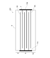
- FIG. 1 is a preferred embodiment of a dielectric element according to the present invention. It is sectional drawing which shows another embodiment of the dielectric material which concerns on this invention.
- FIG. 1 shows a preferred embodiment of a dielectric element according to the present invention.
- a dielectric element 100 shown in FIG. 1 forms a capacitor including a disk-shaped dielectric 1 and a pair of electrodes 2 and 3 formed on both surfaces of the dielectric 1.
- Dielectric 1 is formed of a dielectric ceramic composition represented by the following formula (1).
- A represents at least one element selected from Li, Na, and K.
- a, b, c, d, s, t, u, v, and x are numbers satisfying the following expressions, respectively.
- the dielectric ceramic of the present invention is a combination of ferroelectric compositions. By having this specific combination, a dielectric ceramic composition having a relative dielectric constant at 150 ° C. of 3000 or more and good DC bias characteristics can be obtained.
- the relative dielectric constant at 150 ° C. is less than 3000, the DC bias characteristics are deteriorated, and the withstand voltage is lowered.
- the DC bias characteristics are deteriorated.
- the dielectric constant at 150 ° C. is less than 3000, which is not preferable.
- the content of the composite oxide represented by the formula (1) is 90% by mass or more based on the entire dielectric ceramic composition. It is preferable that impurities such as P and Zr which may be mixed in the manufacturing process may be included.
- the composition of the dielectric ceramic composition can be measured by, for example, fluorescent X-ray analysis or ICP emission spectroscopic analysis.
- the relative density of the dielectric ceramic composition is preferably 95% or more.
- the relative density refers to a measured value of density with respect to the theoretical density.
- the theoretical density is calculated from the lattice constant obtained by X-ray diffraction and the stoichiometric ratio obtained by assuming a perfect crystal.
- the relative density of the dielectric ceramic composition can be measured, for example, by the Archimedes method.
- the relative density of the dielectric ceramic composition can be adjusted by changing the firing temperature and firing time.
- the powder raw material is weighed so that the dielectric ceramic composition (sintered body) after the main firing satisfies the composition of the dielectric ceramic composition according to the present embodiment.
- each raw material powder weighed is wet mixed by a ball mill or the like.
- a calcined product is obtained by calcining the mixture obtained by wet mixing.
- the calcination is usually performed in air.
- the calcination temperature is preferably 700 to 900 ° C., and the calcination time is preferably 1 to 10 hours.
- the obtained calcined product is wet pulverized with a ball mill or the like and then dried to obtain a calcined powder.
- a small amount of a binder is added to the obtained calcined powder and press-molded to obtain a molded body.
- the molding pressure is preferably about 5 t / cm 2 .
- the shape of a molded object For example, it can be set as the disk shaped molded object of planar dimension (PHI) 17mm and thickness about 1mm.
- a dielectric ceramic composition sample is obtained by firing the obtained molded body.
- the firing is usually performed in air.
- the firing temperature is preferably 950 to 1300 ° C., and the firing time is preferably 2 to 10 hours.
- metal electrodes such as silver are formed on both surfaces of the obtained dielectric ceramic composition sample.
- the electrodes are formed by methods such as vapor deposition, sputtering, baking, and electroless plating.
- FIG. 2 is a cross-sectional view showing another embodiment of the dielectric element according to the present invention.
- a laminated dielectric element 200 shown in FIG. 2 includes a rectangular parallelepiped laminated body 5 and a pair of terminal electrodes 11 ⁇ / b> A and 11 ⁇ / b> B respectively formed on opposite end surfaces of the laminated body 5.
- the laminated body 5 includes an element body 8 formed by alternately laminating internal electrode layers (electrode layers) 6A and 6B via a dielectric layer 7, and the element body 8 is arranged on both end surfaces in the laminating direction (upper and lower sides in the figure). It is comprised from a pair of protective layers 9 and 10 provided so that it may be inserted
- the dielectric layer 7 is a layer made of the dielectric ceramic composition according to the present invention.
- the thickness per layer of the dielectric layer 7 can be arbitrarily set, and can be set to 1 to 100 ⁇ m, for example.
- the internal electrode layers 6A and 6B are provided in parallel to each other.
- the internal electrode layer 6 ⁇ / b> A is formed so that one end is exposed on the end surface of the multilayer body 5 where the terminal electrode 11 ⁇ / b> A is formed.
- the internal electrode layer 6B is formed so that one end portion is exposed on the end surface of the multilayer body 5 where the terminal electrode 11B is formed.
- the internal electrode layer 6A and the internal electrode layer 6B are arranged so that most of them overlap in the stacking direction.
- a metal such as Au, Pt, or Ag is used as the material of the internal electrode layers 6A and 6B.
- the terminal electrodes 11A and 11B are in contact with the end portions of the internal electrode layers 6A and 6B exposed at the end surfaces at the end surfaces of the multilayer body 5 on which the terminal electrodes 11A and 11B are provided. Thereby, terminal electrode 11A, 11B is electrically connected with internal electrode layer 6A, 6B, respectively.
- the terminal electrodes 11A and 11B can be made of a conductive material whose main component is Ag, Au, Cu or the like.
- the thicknesses of the terminal electrodes 11A and 11B are appropriately set depending on the application, the size of the multilayer dielectric element, and the like, but can be set to 10 to 50 ⁇ m, for example.
- the dielectric ceramic composition and the dielectric element of the present embodiment have been described.
- the dielectric ceramic composition has a high relative dielectric constant even at a high temperature of 150 ° C. or higher, and when a high electric field is applied. Since the DC bias characteristic is good, for example, it can be suitably used for a medium to high voltage capacitor having a relatively high rated voltage.
- the present invention is not limited to the above embodiment.
- a known element can be used as a configuration other than the dielectric ceramic composition.
- the calcined powder can be produced by a hydrothermal synthesis method or the like.
- (BiNa) TiO 3 , (BiK) TiO 3 , BaTiO 3 , and NaNbO 3 can be prepared, mixed, and sintered as precursors.
- Example 1 to 35 Comparative Examples 1 to 23
- bismuth oxide (Bi 2 O 3 ), sodium carbonate (Na 2 CO 3 ), potassium carbonate (K 2 CO 3 ), barium carbonate (BaCO 3 ), titanium oxide (TiO 2 ) and niobium oxide (Nb 2 O 5 ) powder were prepared.
- a powder of lithium carbonate (Li 2 CO 3 ) was also prepared.
- a powder of potassium carbonate (K 2 CO 3 ) was also prepared.
- a, b, c, d, s + u, t, v, and x in Table 1 are numerical values of a, b, c, d, s + u, t, v, and x in the following formula (1), respectively. Indicates.
- the A component is Na
- Example 5 is the A component Li
- Example 6 is K
- Example 7 is Na and K.
- each raw material powder weighed was wet mixed by a ball mill, and the obtained mixture was calcined in air at 850 ° C. for 2 hours to obtain a calcined product.
- the obtained calcined product was wet pulverized by a ball mill to obtain a calcined powder.
- a small amount of binder was added to the calcined powder, and it was molded at a pressure of about 5 t / cm 2 to obtain a disk-shaped molded body having a planar dimension of ⁇ 17 mm and a thickness of about 1 mm.
- the obtained molded body is fired in the air at a firing temperature of 950 to 1300 ° C. and a firing time of 2 to 10 hours under a relative density of 95% to obtain a dielectric ceramic composition sample. It was.
- the density measurement was performed on the obtained dielectric ceramic sample, the density of all the samples was 95% or more of the theoretical density.
- composition of the obtained dielectric ceramic composition sample was analyzed, it was equal to the weighed composition ratio.
- An Ag electrode was vapor-deposited on both surfaces of the obtained dielectric ceramic composition sample to produce a dielectric element.
- the relative dielectric constant of each dielectric element obtained was measured under a 2 V / ⁇ m DC applied electric field.
- Table 1 shows the dielectric constant at room temperature and 150 ° C., and further the dielectric constant at 150 ° C. and 2 V / ⁇ m DC applied electric field.
- the bar portion in the table indicates that charge leaked during measurement and the value was not obtained.
- those that did not break down were indicated by ⁇ , and those that did break down were indicated by ⁇ .
- Those having a relative dielectric constant at 150 ° C. of 3000 or more and a relative dielectric constant of 2000 or more under a direct current applied electric field of 2 V / ⁇ m were judged to be good.
- the dielectric ceramic compositions of Examples 01 to 35 had a sufficiently large dielectric constant when a high electric field was applied, and had a high dielectric constant even at a high temperature of 150 ° C. or higher.
Landscapes
- Engineering & Computer Science (AREA)
- Chemical & Material Sciences (AREA)
- Ceramic Engineering (AREA)
- Manufacturing & Machinery (AREA)
- Materials Engineering (AREA)
- Power Engineering (AREA)
- Inorganic Chemistry (AREA)
- Structural Engineering (AREA)
- Organic Chemistry (AREA)
- Physics & Mathematics (AREA)
- Microelectronics & Electronic Packaging (AREA)
- Data Mining & Analysis (AREA)
- Mathematical Physics (AREA)
- Theoretical Computer Science (AREA)
- General Physics & Mathematics (AREA)
- Thermal Sciences (AREA)
- Databases & Information Systems (AREA)
- Mathematical Optimization (AREA)
- Mathematical Analysis (AREA)
- Pure & Applied Mathematics (AREA)
- Algebra (AREA)
- Software Systems (AREA)
- General Engineering & Computer Science (AREA)
- Computational Mathematics (AREA)
- Inorganic Insulating Materials (AREA)
- Compositions Of Oxide Ceramics (AREA)
- Ceramic Capacitors (AREA)
- Fixed Capacitors And Capacitor Manufacturing Machines (AREA)
Abstract
【課題】150℃以上の高温度下において3000以上の高い誘電率を有し、さらに直流印加電界2V/μmにおける比誘電率が実用上十分大きい誘電体磁器組成物と、その誘電体磁器組成物を用いた誘電体素子を提供すること。 【解決手段】下記式(1)で表される複合酸化物である誘電体磁器組成物。 {[(BisNat)a (BiuKv)bBac]1-dNad}xTi1-dNbdO3…(1) [式(1)中、a、b、c、d、s、t、u、v及びxは、それぞれ、下記式を満たす数である。] 0.20≦a<0.95 0.00<b≦0.50 0.20<a<0.70のとき、b<(1.20-a)/2 0.05≦c<0.60 0.20<a<0.70のとき、c>(0.80-a)/2 a+b+c=1 0.02≦d<0.10 0.90≦s+u≦1.00 0.45≦t≦0.50 0.45≦v≦0.50 0.95≦x≦1.05
Description
本発明は、誘電体磁器組成物およびこれを用いた電子部品に係り、さらに詳しくは、比較的に定格電圧が高い中高圧用途に好適に用いられる誘電体磁器組成物および誘電体素子に関する。
近年、電子回路の高密度化に伴う電子部品の小型化に対する要求は高く、積層セラミックコンデンサの小型・大容量化が急速に進むとともに、用途も拡大し、要求される特性は様々である。
例えば、ECM(エンジンエレクトリックコンピュータモジュール)、燃料噴射装置、電子制御スロットル、インバータ、コンバータ、HIDヘッドランプユニット、ハイブリッドエンジンのバッテリコントロールユニット、デジタルスチールカメラ等の機器に用いられる定格電圧が100Vを超えるような中高圧用コンデンサには、高い電界強度下において高い静電容量が要求される。
しかしながら、従来の誘電体セラミック組成物は、例えば1V/μm程度の低電界強度の直流電圧下で使用されることを前提に設計されていたので、用いられる積層セラミックコンデンサの薄層化が進んで、高い電界強度下で使用されると、印加直流電界に対する静電容量の変化率(以下DCバイアス変化率)が大きくなり、実効容量が低下するという問題があった。
DCバイアス変化率が大きいと、積層セラミックコンデンサの実効容量が低下してしまい、設計の段階で必要としていた静電容量を満たさなくなるため、それが用いられている電子機器の動作が不安定になり、延いては動作しなくなるという不具合が発生することが懸念される。
また、このような積層セラミックコンデンサを中高圧用コンデンサとして用いる場合、電子部品の高密度の実装により生じる発熱や、自動車用電子部品に代表される過酷な使用環境が問題となるため、印加直流電圧(DCバイアス)が印可された状態で、150℃以上の高温度下においても高い静電容量を得ることが望まれるようになってきている。
したがって、高電界下での利用を目的としたコンデンサにはDCバイアス変化率が小さい、つまり高電界印加時の比誘電率が実用上十分大きく、150℃以上の高温度下においても高い比誘電率を有する誘電体磁器組成物を用いることが望ましい。なお、ここで言う高電界とはたとえば2V/μmの電界強度、高い比誘電率とは例えば2000を指す。
このような課題を解決するべく、下記の特許文献1では、金属元素として少なくともSr、Ba、Pb、Bi、Tiを含有し、これらの金属元素の原子比による組成式を(Sr1-v-w-x-yBavCawPbxBiy)TizO3+aと表した時、前記v、w、x、yおよびzが
0.01≦v≦0.05
0 ≦w≦0.20
0.05≦x≦0.20
0.01≦y≦0.30
1.00≦z≦1.20
v+w+x+y≦0.50
aは過剰酸素量を満足するものを主成分とし、この主成分100重量部に対して、LiおよびBのうち少なくとも1種を含有するガラス成分を0.1~10.0重量部の割合で含有し、かつペロブスカイト型結晶相を主結晶相とする誘電体磁器組成物が開示されている。
0.01≦v≦0.05
0 ≦w≦0.20
0.05≦x≦0.20
0.01≦y≦0.30
1.00≦z≦1.20
v+w+x+y≦0.50
aは過剰酸素量を満足するものを主成分とし、この主成分100重量部に対して、LiおよびBのうち少なくとも1種を含有するガラス成分を0.1~10.0重量部の割合で含有し、かつペロブスカイト型結晶相を主結晶相とする誘電体磁器組成物が開示されている。
しかしながら、特許文献1に示すような誘電体磁器組成物は、2V/μmのDCバイアス印加による比誘電率の変化率が-10%以内と良好であるが、比誘電率が1500程度と比較的小さいことが問題となっていた。また、85℃までの温度変化率しか記載されておらず、高温での使用を目的としていない。
本発明は、このような実状に鑑みてなされ、その目的は、比較的に定格電圧が高い中高圧用途に好適に用いられ、150℃以上の高温度下において3000以上の高い誘電率を有し、さらに直流印加電界2V/μmにおける比誘電率が実用上十分大きい誘電体磁器組成物と、その誘電体磁器組成物を用いた誘電体素子を提供することである
上記目的を達成するため、本発明は、下記式(1)で表される複合酸化物である誘電体磁器組成物を提供する。
{[(BisNat)a (BiuKv)bBac]1-dAd}xTi1-dNbdO3…(1)
式(1)中、AはLi、Na、Kから選ばれる少なくとも一種の元素を示す。a、b、c、d、s、t、u、v及びxは、それぞれ、下記式を満たす数である。
式(1)中、AはLi、Na、Kから選ばれる少なくとも一種の元素を示す。a、b、c、d、s、t、u、v及びxは、それぞれ、下記式を満たす数である。
0.20≦a<0.95
0.00<b≦0.50
0.20<a<0.70のとき、b<(1.20-a)/2
0.05≦c<0.60
0.20<a<0.70のとき、c>(0.80-a)/2
a+b+c=1
0.02≦d<0.10
0.90≦s+u≦1.00
0.45≦t≦0.50
0.45≦v≦0.50
0.95≦x≦1.05
0.00<b≦0.50
0.20<a<0.70のとき、b<(1.20-a)/2
0.05≦c<0.60
0.20<a<0.70のとき、c>(0.80-a)/2
a+b+c=1
0.02≦d<0.10
0.90≦s+u≦1.00
0.45≦t≦0.50
0.45≦v≦0.50
0.95≦x≦1.05
本発明の誘電体磁器組成物は、上記構成を有することにより、150℃以上の高温度下において3000以上の高い誘電率を有し、さらに直流印加電界2V/μmにおける比誘電率が2000以上と高い比誘電率を得られる。
また、本発明は、上記誘電体磁器組成物を備える誘電体素子を提供する。
このような誘電体素子は上記誘電体磁器組成物を備えるため、高電界を印加した場合に大きな誘電率を必要とする、例えば高電界印加回路に使用される回路保護用などのコンデ
ンサに有用である。
ンサに有用である。
本発明によれば、比較的に定格電圧が高い中高圧用途に好適に用いられ、150℃以上の高温度下において3000以上の高い誘電率を有し、さらに直流印加電界2V/μmにおける比誘電率が実用上十分大きい誘電体磁器組成物と、その誘電体磁器組成物を用いた誘電体素子を提供することができる。
以下、場合により図面を参照して、本発明の好適な実施形態について説明する。なお、各図面において、同一または同等の要素には同一の符号を付与し、重複する説明を省略する。
図1は本発明に係る誘電体素子の好適な一実施形態である。図1に示す誘電体素子100は、円盤状の誘電体1と、この誘電体1の両面に形成された一対の電極2および3を備えたコンデンサを形成している。
誘電体1は、下記式(1)で示される誘電体磁器組成物で形成される。
{[(BisNat)a (BiuKv)bBac]1-dAd}xTi1-dNbdO3…(1)
式(1)中、AはLi、Na、Kから選ばれる少なくとも一種の元素を示す。a、b、c、d、s、t、u、v及びxは、それぞれ、下記式を満たす数である。
0.20≦a<0.95
0.00<b≦0.50
0.20<a<0.70のとき、b<(1.20-a)/2
0.05≦c<0.60
0.20<a<0.70のとき、c>(0.80-a)/2
a+b+c=1
0.02≦d<0.10
0.90≦s+u≦1.00
0.45≦t≦0.50
0.45≦v≦0.50
0.95≦x≦1.05
0.00<b≦0.50
0.20<a<0.70のとき、b<(1.20-a)/2
0.05≦c<0.60
0.20<a<0.70のとき、c>(0.80-a)/2
a+b+c=1
0.02≦d<0.10
0.90≦s+u≦1.00
0.45≦t≦0.50
0.45≦v≦0.50
0.95≦x≦1.05
このような誘電体磁器組成物は、上記構成を有することにより、高電界を印加した場合でも大きな比誘電率を得られる。
本発明の誘電体磁器は強誘電体組成物の組み合わせであり、この特定の組み合わせを有することにより150℃における比誘電率が3000以上でDCバイアス特性が良好な誘電体磁器組成物を得られる。
a、b、cが上記範囲をはずれると、150℃における比誘電率が3000未満となってしまったり、DCバイアス特性が悪くなってしまったり、耐電圧が低くなってしまうた
め好ましくない。
め好ましくない。
dが0.02未満ではDCバイアス特性が悪くなってしまい、0.10以上では150℃における誘電率が3000未満となってしまうため好ましくない。
s+u、t、vが上記範囲を外れると欠陥が生成されたり、十分な焼結密度が得られず、電荷のリークが生じたり、耐電圧が低くなってしまうため好ましくない。
xが0.95未満又は1.05を超えると十分な焼結密度を得られず、絶縁抵抗が低くなるため、高電界を印加して使用することは困難になる。
誘電体磁器組成物として実用に十分な誘電率が得られる等の観点から、式(1)で表される複合酸化物の含有量は、誘電体磁器組成物全体を基準として、90質量%以上であることが好ましく、作製プロセス上混入する可能性があるP、Zrなどの不純物を含んでいても良い。
ここで、誘電体磁器組成物の組成は、例えば、蛍光X線分析やICP発光分光分析で測定することができる。
上記誘電体磁器組成物の相対密度は、95%以上の相対密度を有することが好ましい。ここで、本明細書において、相対密度とは、理論密度に対する、密度の実測値をいう。なお、理論密度は、X線回折によって求めた格子定数と、完全結晶を仮定して求めた量論比により計算される。誘電体磁器組成物の相対密度は、例えば、アルキメデス法によって測定することができる。ここで、誘電体磁器組成物の相対密度は、焼成温度や焼成時間を変えることによって調整することができる。
次に、図1に示す誘電体素子の製造方法の一例について以下に説明する。
まず、誘電体1の出発原料として、酸化ビスマス(Bi2O3)、炭酸ナトリウム(Na2CO3)、炭酸カリウム(K2CO3)、炭酸バリウム(BaCO3)、酸化チタン(TiO2)及び酸化二オブ(Nb2O5)等の粉末を準備する。
そして、本焼成後の誘電体磁器組成物(焼結体)が、本実施形態に係る誘電体磁器組成物の組成を満たすものとなるように、上記粉末原料を秤量する。
次に、秤量した各原料粉末を、ボールミル等により湿式混合する。そして、湿式混合により得られた混合物を仮焼することにより仮焼物を得る。ここで、仮焼は、通常空気中で施される。また、仮焼温度は700~900℃であることが好ましく、仮焼時間は1~10時間が好ましい。
得られた仮焼物を、ボールミル等で湿式粉砕した後、これを乾燥させることにより、仮焼物粉体を得る。次いで、得られた仮焼物粉体に少量の結合剤を添加し、プレス成形することにより、成形体を得る。ここで、成形圧力は5t/cm2程度であることが好ましい。成形体の形状に特に制限はなく、例えば、平面寸法Φ17mm、厚さ1mm程度の円板状成形体とすることができる。
そして、得られた成形体を焼成することにより誘電体磁器組成物試料を得る。ここで、焼成は、通常空気中で施される。また、焼成温度は950~1300℃であることが好ましく、焼成時間は2~10時間であることが好ましい。
次いで、得られた誘電体磁器組成物試料の両面に、銀等の金属電極を形成する。電極の形成は蒸着、スパッタリング、焼付け、無電解めっき等の方法による。
図2は本発明に係る誘電体素子の別の実施形態を示す断面図である。図2に示す積層型誘電体素子200は、直方体状の積層体5と、この積層体5の対向する端面にそれぞれ形成された一対の端子電極11A、11Bとを備えている。
積層体5は、誘電体層7を介して内部電極層(電極層)6A、6Bを交互に積層してなる素体8と、この素体8をその積層方向の両端面側(図中上下方向)から挟み込むように設けられた一対の保護層9及び10とから構成される。素体8においては、誘電体層7と内部電極層6A、6Bとが交互に積層されている。
誘電体層7は、本発明に係る誘電体磁器組成物からなる層である。
誘電体層7の1層当たりの厚さは、任意に設定することができるが、例えば1~100μmにすることができる。
内部電極層6A、6Bはそれぞれ平行となるように設けられている。内部電極層6Aは、一方の端部が積層体5における端子電極11Aが形成された端面に露出するように形成されている。また、内部電極層6Bは、一方の端部が積層体5における端子電極11Bが形成された端面に露出するように形成されている。さらに、内部電極層6Aと内部電極層6Bとは、これらの大部分が積層方向に重なり合うように配置されている。
内部電極層6A、6Bの材質としては、例えば、Au,Pt若しくはAg等の金属が用いられる。
端子電極11A,11Bは、これらが設けられている積層体5の端面において、当該端面に露出している内部電極層6A、6Bの端部とそれぞれ接している。これにより、端子電極11A,11Bは、内部電極層6A、6Bとそれぞれ電気的に接続される。この端子電極11A,11Bは、Ag,Au,Cu等を主成分とする導電材料から構成することができる。端子電極11A,11Bの厚さは、用途や積層型誘電素子のサイズ等によって適宜設定されるが、例えば10~50μmにすることができる。
以上、本実施形態の誘電体磁器組成物および誘電体素子について説明したが、当該誘電体磁器組成物は、150℃以上の高温でも高い比誘電率を有し、また高電界を印加した時のDCバイアス特性が良好であるため、例えば、比較的に定格電圧が高い中高圧コンデンサに好適に用いることができる。
また、本発明は上記実施形態に限定されるものではない。例えば、上記誘電体素子において、誘電体磁器組成物以外の構成として、公知のものを用いることもできる。また、例えば、上記誘電体素子の製造において、当該仮焼物粉体を水熱合成法等により製造することもできる。また、前駆体として(BiNa)TiO3、(BiK)TiO3、BaTiO3、およびNaNbO3を作製し、混合、焼結することもできる。
以下、実施例及び比較例を用いて、本発明を更に詳細に説明する。ただし、本発明は以下の実施例に限定されるものではない。
(実施例1~35、比較例1~23)
誘電体磁器組成物を作製するため、出発原料として、酸化ビスマス(Bi2O3)、炭
酸ナトリウム(Na2CO3)、炭酸カリウム(K2CO3)、炭酸バリウム(BaCO3)、酸化チタン(TiO2)及び酸化二オブ(Nb2O5)の粉末を準備した。実施例5については上記に加えさらに炭酸リチウム(Li2CO3)の粉末も準備した。実施例6および実施例7については上記に加えさらに炭酸カリウム(K2CO3)の粉末も準備した。
誘電体磁器組成物を作製するため、出発原料として、酸化ビスマス(Bi2O3)、炭
酸ナトリウム(Na2CO3)、炭酸カリウム(K2CO3)、炭酸バリウム(BaCO3)、酸化チタン(TiO2)及び酸化二オブ(Nb2O5)の粉末を準備した。実施例5については上記に加えさらに炭酸リチウム(Li2CO3)の粉末も準備した。実施例6および実施例7については上記に加えさらに炭酸カリウム(K2CO3)の粉末も準備した。
本焼成後の誘電体磁器組成物(焼結体)が、表1の組成を満たすものとなるように、上記粉末原料を秤量した。なお、ここで、表1中のa、b、c、d、s+u、t、v及びxは、それぞれ下記式(1)におけるa、b、c、d、s+u、t、v及びxの数値を示す。実施例5~7以外の実施例および比較例については、A成分がNaであり、実施例5はA成分がLi、実施例6はK、実施例7はNaおよびKとなる。
{[(BisNat)a (BiuKv)bBac]1-dAd}xTi1-dNbdO3…(1)
次に、秤量した各原料粉末を、ボールミルにより湿式混合した後、得られた混合物を、空気中において850℃で2時間仮焼して仮焼物を得た。そして、得られた仮焼物をボールミルで湿式粉砕して、仮焼物粉体を得た。次いで、仮焼物粉体に少量の結合剤を添加し、約5t/cm2の圧力で成形し、平面寸法Φ17mm、厚さ1mm程度の円板状成形体を得た。
次に、得られた成形体を空気中において、焼成温度950~1300℃、焼成時間2~10時間の範囲で、相対密度95%となる条件で焼成して、誘電体磁器組成物試料を得た。得られた誘電磁器試料について密度測定を行ったところ、すべての試料の密度が、理論密度に対し95%以上であった。
得られた誘電体磁器組成物試料の組成を分析したところ、秤量した組成比と等しかった。
得られた誘電体磁器組成物試料の両面にAg電極を蒸着し、誘電体素子を作製した。
得られた各誘電体素子の2V/μm直流印加電界下での比誘電率測定を実施した。
室温および150℃での比誘電率、さらに150℃かつ2V/μm直流印加電界下での比誘電率を表1に示す。また、表中の棒線部は測定時に電荷がリークしてしまい、値が得られなかったことを示す。また、表中の耐電圧試験の項で、絶縁破壊しなかったものは○、絶縁破壊したものは×で示した。150℃での比誘電率が3000以上、かつ2V/μmの直流印加電界下での比誘電率が2000以上であるものを良好と判断した。

以上より、実施例01~35の誘電体磁器組成物は高電界印加時の誘電率が実用上十分大きく、150℃以上の高温度下においても高い誘電率を有することを確認した。
1…誘電体、2,3…電極、5…積層体、6A、6B…内部電極層、7…誘電体層、8…素体、9、10…保護層、11A,11B…端子電極、100…誘電体素子、200…積層誘電体素子
Claims (2)
- 下記一般式(1)の組成を有することを特徴とする誘電体磁器組成物。
{[(BisNat)a (BiuKv)bBac]1-dAd}xTi1-dNbdO3…(1)
式(1)中、AはLi、Na、Kから選ばれる少なくとも一種の元素を示す。a、b、c、d、s、t、u、v及びxは、それぞれ、下記式を満たす数である。
0.20≦a<0.95
0.00<b≦0.50
0.20<a<0.70のとき、b<(1.20-a)/2
0.05≦c<0.60
0.20<a<0.70のとき、c>(0.80-a)/2
a+b+c=1
0.02≦d<0.10
0.90≦s+u≦1.00
0.45≦t≦0.50
0.45≦v≦0.50
0.95≦x≦1.05 - 請求項1に記載の誘電体磁器組成物を備える誘電体素子。
Priority Applications (1)
| Application Number | Priority Date | Filing Date | Title |
|---|---|---|---|
| US14/759,539 US9530562B2 (en) | 2013-03-27 | 2014-02-04 | Dielectric ceramic composition and dielectric device |
Applications Claiming Priority (2)
| Application Number | Priority Date | Filing Date | Title |
|---|---|---|---|
| JP2013066572A JP6102405B2 (ja) | 2013-03-27 | 2013-03-27 | 誘電体磁器組成物、および誘電体素子 |
| JP2013-066572 | 2013-03-27 |
Publications (1)
| Publication Number | Publication Date |
|---|---|
| WO2014156301A1 true WO2014156301A1 (ja) | 2014-10-02 |
Family
ID=51623302
Family Applications (1)
| Application Number | Title | Priority Date | Filing Date |
|---|---|---|---|
| PCT/JP2014/052479 Ceased WO2014156301A1 (ja) | 2013-03-27 | 2014-02-04 | 誘電体磁器組成物、および誘電体素子 |
Country Status (3)
| Country | Link |
|---|---|
| US (1) | US9530562B2 (ja) |
| JP (1) | JP6102405B2 (ja) |
| WO (1) | WO2014156301A1 (ja) |
Cited By (1)
| Publication number | Priority date | Publication date | Assignee | Title |
|---|---|---|---|---|
| CN119751063A (zh) * | 2025-03-07 | 2025-04-04 | 杭州兴容科技有限公司 | 一种x9r型mlcc陶瓷材料及其制备方法 |
Families Citing this family (4)
| Publication number | Priority date | Publication date | Assignee | Title |
|---|---|---|---|---|
| JP6102410B2 (ja) * | 2013-03-28 | 2017-03-29 | Tdk株式会社 | 誘電体磁器組成物、および誘電体素子 |
| JP2016060647A (ja) * | 2014-09-12 | 2016-04-25 | エプコス アクチエンゲゼルシャフトEpcos Ag | 誘電体組成物、誘電体素子、電子部品および積層電子部品 |
| KR102089701B1 (ko) * | 2015-10-21 | 2020-03-16 | 삼성전기주식회사 | 유전체 자기 조성물 및 이를 포함하는 적층 세라믹 커패시터 |
| JP7439917B2 (ja) * | 2020-05-12 | 2024-02-28 | 株式会社村田製作所 | 誘電体組成物および積層セラミックコンデンサ |
Citations (1)
| Publication number | Priority date | Publication date | Assignee | Title |
|---|---|---|---|---|
| JP2002321976A (ja) * | 2001-02-22 | 2002-11-08 | Tdk Corp | 圧電磁器 |
Family Cites Families (3)
| Publication number | Priority date | Publication date | Assignee | Title |
|---|---|---|---|---|
| JP3814401B2 (ja) | 1998-01-30 | 2006-08-30 | 京セラ株式会社 | 誘電体磁器および積層セラミックコンデンサ |
| JP4674405B2 (ja) * | 2000-11-21 | 2011-04-20 | Tdk株式会社 | 圧電磁器 |
| JP6102410B2 (ja) * | 2013-03-28 | 2017-03-29 | Tdk株式会社 | 誘電体磁器組成物、および誘電体素子 |
-
2013
- 2013-03-27 JP JP2013066572A patent/JP6102405B2/ja active Active
-
2014
- 2014-02-04 WO PCT/JP2014/052479 patent/WO2014156301A1/ja not_active Ceased
- 2014-02-04 US US14/759,539 patent/US9530562B2/en active Active
Patent Citations (1)
| Publication number | Priority date | Publication date | Assignee | Title |
|---|---|---|---|---|
| JP2002321976A (ja) * | 2001-02-22 | 2002-11-08 | Tdk Corp | 圧電磁器 |
Non-Patent Citations (5)
| Title |
|---|
| DITTMER,ROBERT ET AL.: "A High-Temperature- Capacitor Dielectric Based on K0.5Na0.5Nbo3- Modified Bi1/2Na1/2Tio3-Bi1/2K1/2Tio3", JOURNAL OF THE AMERICAN CERAMIC SOCIETY, vol. 95, no. 11, November 2012 (2012-11-01), pages 3519 - 3524 * |
| DITTMER,ROBERT ET AL.: "Lead-free high- temperature dielectrics with wide operational range", JOURNAL OF APPLIED PHYSICS, vol. 109, 2011, pages 034107-1 - 034107-5 * |
| LIU,YANG ET AL.: "TEMPERATURE-INDEPENDENT DIELECTRIC PROPERTIES OF 0.82[0.94Bi0.5Na 0.5TiO3-0.06BaTiO3]-0.18K0.5Na0.5NbO3 CERAMICS", JOURNAL OF ADVANCED DIELECTRICS, vol. 2, no. 1, 2012, pages 1250006-1 - 1250006-6 * |
| RODEL,JURGEN ET AL.: "Electric-Field Effects in Bi-based Perovskites", 3RD INTERNATIONAL CONGRESS ON CERAMICS (ICC3) MEETING GUIDE, 14 November 2010 (2010-11-14) * |
| ZHU,MANKANG ET AL.: "Dependence of depolarization temperature on cation vacancies and lattice distortion for lead-free 74(Bil/ 2Na1/2)TiO3-20.8(Bi1/2K1/2)TiO3-5.2BaTiO3 ferroelectric ceramics", APPLIED PHISICS LETTERS, vol. 94, 2009, pages 182901-1 - 182901-3 * |
Cited By (1)
| Publication number | Priority date | Publication date | Assignee | Title |
|---|---|---|---|---|
| CN119751063A (zh) * | 2025-03-07 | 2025-04-04 | 杭州兴容科技有限公司 | 一种x9r型mlcc陶瓷材料及其制备方法 |
Also Published As
| Publication number | Publication date |
|---|---|
| JP6102405B2 (ja) | 2017-03-29 |
| JP2014189443A (ja) | 2014-10-06 |
| US20150348709A1 (en) | 2015-12-03 |
| US9530562B2 (en) | 2016-12-27 |
Similar Documents
| Publication | Publication Date | Title |
|---|---|---|
| JP6102410B2 (ja) | 誘電体磁器組成物、および誘電体素子 | |
| EP3191427B1 (en) | Dielectric composition, dielectric element, electronic component and laminated electronic component | |
| JP6316985B2 (ja) | 誘電体組成物、誘電体素子、電子部品および積層電子部品 | |
| CN105916829B (zh) | 介电组合物、介电元件、电子部件和层叠电子部件 | |
| JP6102405B2 (ja) | 誘電体磁器組成物、および誘電体素子 | |
| WO2023074139A1 (ja) | 圧電素子、および圧電素子の製造方法 | |
| US9911536B2 (en) | Dielectric composition, dielectric element, electronic component and laminated electronic component | |
| JP2004210613A (ja) | 誘電体磁器、その製造方法、及び積層セラミックコンデンサ |
Legal Events
| Date | Code | Title | Description |
|---|---|---|---|
| 121 | Ep: the epo has been informed by wipo that ep was designated in this application |
Ref document number: 14775801 Country of ref document: EP Kind code of ref document: A1 |
|
| WWE | Wipo information: entry into national phase |
Ref document number: 14759539 Country of ref document: US |
|
| NENP | Non-entry into the national phase |
Ref country code: DE |
|
| 122 | Ep: pct application non-entry in european phase |
Ref document number: 14775801 Country of ref document: EP Kind code of ref document: A1 |