WO2014148208A1 - 電子制御装置及びデータ書換え方法 - Google Patents
電子制御装置及びデータ書換え方法 Download PDFInfo
- Publication number
- WO2014148208A1 WO2014148208A1 PCT/JP2014/054484 JP2014054484W WO2014148208A1 WO 2014148208 A1 WO2014148208 A1 WO 2014148208A1 JP 2014054484 W JP2014054484 W JP 2014054484W WO 2014148208 A1 WO2014148208 A1 WO 2014148208A1
- Authority
- WO
- WIPO (PCT)
- Prior art keywords
- data
- processor
- nonvolatile memory
- written
- tool
- Prior art date
- Legal status (The legal status is an assumption and is not a legal conclusion. Google has not performed a legal analysis and makes no representation as to the accuracy of the status listed.)
- Ceased
Links
Images





Classifications
-
- G—PHYSICS
- G11—INFORMATION STORAGE
- G11C—STATIC STORES
- G11C16/00—Erasable programmable read-only memories
- G11C16/02—Erasable programmable read-only memories electrically programmable
- G11C16/06—Auxiliary circuits, e.g. for writing into memory
- G11C16/10—Programming or data input circuits
- G11C16/14—Circuits for erasing electrically, e.g. erase voltage switching circuits
- G11C16/16—Circuits for erasing electrically, e.g. erase voltage switching circuits for erasing blocks, e.g. arrays, words, groups
-
- G—PHYSICS
- G05—CONTROLLING; REGULATING
- G05B—CONTROL OR REGULATING SYSTEMS IN GENERAL; FUNCTIONAL ELEMENTS OF SUCH SYSTEMS; MONITORING OR TESTING ARRANGEMENTS FOR SUCH SYSTEMS OR ELEMENTS
- G05B15/00—Systems controlled by a computer
- G05B15/02—Systems controlled by a computer electric
-
- G—PHYSICS
- G06—COMPUTING OR CALCULATING; COUNTING
- G06F—ELECTRIC DIGITAL DATA PROCESSING
- G06F12/00—Accessing, addressing or allocating within memory systems or architectures
-
- G—PHYSICS
- G06—COMPUTING OR CALCULATING; COUNTING
- G06F—ELECTRIC DIGITAL DATA PROCESSING
- G06F12/00—Accessing, addressing or allocating within memory systems or architectures
- G06F12/02—Addressing or allocation; Relocation
- G06F12/0223—User address space allocation, e.g. contiguous or non contiguous base addressing
- G06F12/023—Free address space management
- G06F12/0238—Memory management in non-volatile memory, e.g. resistive RAM or ferroelectric memory
- G06F12/0246—Memory management in non-volatile memory, e.g. resistive RAM or ferroelectric memory in block erasable memory, e.g. flash memory
-
- G—PHYSICS
- G06—COMPUTING OR CALCULATING; COUNTING
- G06F—ELECTRIC DIGITAL DATA PROCESSING
- G06F3/00—Input arrangements for transferring data to be processed into a form capable of being handled by the computer; Output arrangements for transferring data from processing unit to output unit, e.g. interface arrangements
- G06F3/06—Digital input from, or digital output to, record carriers, e.g. RAID, emulated record carriers or networked record carriers
- G06F3/0601—Interfaces specially adapted for storage systems
- G06F3/0602—Interfaces specially adapted for storage systems specifically adapted to achieve a particular effect
- G06F3/061—Improving I/O performance
-
- G—PHYSICS
- G06—COMPUTING OR CALCULATING; COUNTING
- G06F—ELECTRIC DIGITAL DATA PROCESSING
- G06F3/00—Input arrangements for transferring data to be processed into a form capable of being handled by the computer; Output arrangements for transferring data from processing unit to output unit, e.g. interface arrangements
- G06F3/06—Digital input from, or digital output to, record carriers, e.g. RAID, emulated record carriers or networked record carriers
- G06F3/0601—Interfaces specially adapted for storage systems
- G06F3/0628—Interfaces specially adapted for storage systems making use of a particular technique
- G06F3/0638—Organizing or formatting or addressing of data
- G06F3/064—Management of blocks
-
- G—PHYSICS
- G06—COMPUTING OR CALCULATING; COUNTING
- G06F—ELECTRIC DIGITAL DATA PROCESSING
- G06F3/00—Input arrangements for transferring data to be processed into a form capable of being handled by the computer; Output arrangements for transferring data from processing unit to output unit, e.g. interface arrangements
- G06F3/06—Digital input from, or digital output to, record carriers, e.g. RAID, emulated record carriers or networked record carriers
- G06F3/0601—Interfaces specially adapted for storage systems
- G06F3/0668—Interfaces specially adapted for storage systems adopting a particular infrastructure
- G06F3/0671—In-line storage system
- G06F3/0673—Single storage device
- G06F3/0679—Non-volatile semiconductor memory device, e.g. flash memory, one time programmable memory [OTP]
-
- G—PHYSICS
- G11—INFORMATION STORAGE
- G11C—STATIC STORES
- G11C16/00—Erasable programmable read-only memories
- G11C16/02—Erasable programmable read-only memories electrically programmable
-
- G—PHYSICS
- G06—COMPUTING OR CALCULATING; COUNTING
- G06F—ELECTRIC DIGITAL DATA PROCESSING
- G06F2212/00—Indexing scheme relating to accessing, addressing or allocation within memory systems or architectures
- G06F2212/10—Providing a specific technical effect
- G06F2212/1016—Performance improvement
-
- G—PHYSICS
- G06—COMPUTING OR CALCULATING; COUNTING
- G06F—ELECTRIC DIGITAL DATA PROCESSING
- G06F2212/00—Indexing scheme relating to accessing, addressing or allocation within memory systems or architectures
- G06F2212/72—Details relating to flash memory management
- G06F2212/7201—Logical to physical mapping or translation of blocks or pages
-
- G—PHYSICS
- G06—COMPUTING OR CALCULATING; COUNTING
- G06F—ELECTRIC DIGITAL DATA PROCESSING
- G06F2212/00—Indexing scheme relating to accessing, addressing or allocation within memory systems or architectures
- G06F2212/72—Details relating to flash memory management
- G06F2212/7202—Allocation control and policies
Definitions
- the present invention relates to a technique for rewriting data of an electronic control device.
- Patent Document 1 Japanese Patent Laid-Open No. 9-128229
- an object of the present invention is to provide an electronic control device and a data rewriting method capable of reducing the time required for rewriting data in a nonvolatile memory such as a flash ROM.
- the electronic control unit has a nonvolatile memory that can erase data in units of erase blocks and can write data in units of write blocks smaller than the erase block, and a processor. Then, in response to an external data rewrite request, the processor of the electronic control unit erases a part of the data in the nonvolatile memory in units of erase blocks and stores the data in a part of the nonvolatile memory in units of write blocks. Write.
- the time required for rewriting data in a nonvolatile memory such as a flash ROM can be shortened.
- FIG. 1 shows an example of a data rewriting system for rewriting data of an electronic control unit (ECU) mounted on an automobile.
- ECU electronice control unit
- the ECU 100 to be rewritten is detachably connected to a tool 300 in which an operator performs data rewriting work of the ECU 100 via a network cable 200 such as CAN (ControllerCAArea Network), serial communication, FlexRay (registered trademark) or the like. Is done.
- a network cable 200 such as CAN (ControllerCAArea Network), serial communication, FlexRay (registered trademark) or the like. Is done.
- the ECU 100 and the tool 300 are not limited to being wired using the network cable 200 but may be connected to each other wirelessly using a wireless transceiver.
- the ECU 100 is an electronic device that controls various devices mounted on an automobile, such as a fuel injection valve, a transmission, an electric brake system, an ABS (Antilock Brake System), a variable valve timing mechanism, a brushless motor, and the like.
- the ECU 100 includes a processor 110 such as a CPU (Central Processing Unit), a communication circuit 120 for connecting to a network, a flash ROM 130 as an example of a nonvolatile memory, RAM (Random Access Memory) 140 as an example of a volatile memory, and a bus 150 that connects the processor 110, the communication circuit 120, the flash ROM 130, and the RAM 140 to each other.
- the communication circuit 120 includes a connector (not shown) that detachably connects the network cable 200.
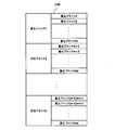
- the flash ROM 130 has a plurality of erase blocks 1 to n having a predetermined size (for example, 32 Kbytes, 64 Kbytes, etc.) and a plurality of writes having a predetermined size (for example, 256 bytes) for each erase block. It is divided into blocks 1 to m.
- the erase block defines the minimum unit for erasing data
- the write block is a concept for defining the minimum unit for writing data, and has the characteristic that the erase block is larger than the write block.
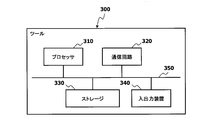
- the tool 300 is an electronic device in which an operator performs data rewriting work of the ECU 100, and includes, for example, a computer such as a personal computer.
- the tool 300 includes a processor 310 such as a CPU, a communication circuit 320 for connecting to a network, a storage 330 such as a hard disk device and an SSD (Solid State Drive), and a work
- An input / output device 340 serving as an interface to a person.
- the communication circuit 320 includes a connector (not shown) that removably connects the network cable 200.
- the input / output device 340 includes a display such as an LCD (Liquid Crystal Display), a keyboard, and a pointing device such as a mouse.
- the storage 330 may be, for example, a NAS (Network Attached Storage) connected to a network (not shown), a server storage, or the like.
- the storage 330 stores rewrite data for rewriting the flash ROM 130 of the ECU 100.
- the rewrite data includes, for example, a control program for controlling various devices mounted on the automobile, constants used in the control program, control parameters such as maps, and the like.
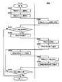
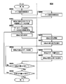
- FIG. 5 shows an example of the first embodiment of the data rewriting process for rewriting data in the flash ROM 130 of the ECU 100.
- the operator designates rewriting data and rewritten data and performs a predetermined operation on the tool 300. Executed. Note that the data rewriting process shown in FIG. 5 is executed for each erase block of rewritten data (the same applies to the second embodiment).
- the ECU 100 is started by being supplied with electric power when connected to the tool 300 via the network cable 200.
- the ECU 100 may be started by connecting another power cable.
- the memory map of the flash ROM 130 in the ECU 100 represents the erase block as “EBn” and the write block as “WBm” (m, n: natural numbers). I will do it.
- step 100 the processor 310 of the tool 300 calculates a hash value of the erase block EBx (x: natural number 1 to n). That is, the processor 310 calculates the hash value of the data of the erase block EBx in the rewritten data using a known hash function such as SHA (Secure Hash Algorithm), MD5 (Message Digest Algorithm 5).
- SHA Secure Hash Algorithm
- MD5 Message Digest Algorithm 5
- the hash value is an example of identification information for easily determining the identity of the data, and a similar value is used even for similar data.
- the processor 310 temporarily stores the hash value calculated from the data of the erase block EBx in a storage medium such as a RAM (not shown).
- step 101 the processor 310 of the tool 300 requests the hash value of the data of the erase block EBx in the rewritten data written in the flash ROM 130, for example, by designating the address of the erase block EBx to the ECU 100. To do.
- step 200 in response to the hash value request from the tool 300, the processor 110 of the ECU 100 calculates the hash value of the data in the erase block EBx starting from the designated address of the rewritten data written in the flash ROM 130.
- the processor 110 calculates a hash value by using the same hash function as that of the tool 300 so that the tool 300 can compare hash values. Then, the processor 110 returns the hash value calculated from the erase block EBx to the tool 300.
- step 102 the processor 310 of the tool 300 determines whether there is a difference between the two hash values by comparing the hash value stored in the storage medium with the hash value returned from the ECU 100. That is, the processor 310 determines whether or not there is a difference in the data of the corresponding erase block between the rewritten data and the rewritten data, in other words, whether or not there is identity. If it is determined that there is a difference between the two hash values, the processor 310 proceeds to step 103 (Yes), and if it is determined that there is no difference between the two hash values, the processing of the erase block EBx is terminated. (No).
- step 103 the processor 310 of the tool 300 requests the ECU 100 to erase the data in the erase block EBx in the flash ROM 130. That is, since there is a difference in the corresponding erase block data between the rewritten data and the rewritten data, the processor 310 erases the erase block EBx from the ECU 100 in order to enable data rewrite of the erase block. Request.
- step 201 in response to the erase request from the tool 300, the processor 110 of the ECU 100 erases the data, for example, by writing predetermined data in the erase block EBx in the flash ROM 130.
- step 202 the processor 110 of the ECU 100 notifies the tool 300 that data erasure of the erase block EBx in the flash ROM 130 has been completed. Such notification is performed to synchronize between the ECU 100 and the tool 300 (the same applies hereinafter).
- step 104 in response to the notification from the ECU 100, the processor 310 of the tool 300 sequentially extracts data of the write block WBy (y: natural number 1 to m) belonging to the erase block EBx from the rewrite data, and this is extracted from the ECU 100. Send to. That is, the processor 310 sequentially transmits to the ECU 100 data to be written in the area where the data has been erased in the storage area of the flash ROM 130 of the ECU 100.
- step 203 the processor 110 of the ECU 100 writes the data received from the tool 300 into the write block WBy of the flash ROM 130.
- step 204 the processor 110 of the ECU 100 notifies the tool 300 that the data writing to the writing block WBy of the flash ROM 130 has been completed.
- step 105 in response to the notification from the ECU 100, the processor 310 of the tool 300 has completed writing of data to the erase block EBx through, for example, whether or not the processing has been completed up to the write block WBm. Determine whether or not. Then, the processor 310 terminates the process of the erase block EBx if it is determined that the data writing is completed (Yes), and returns the process to step 104 if it is determined that the data writing is not completed (No).
- the tool 300 transmits a data erase request for the erase block having the difference to the ECU 100, and Data for writing to the write block belonging to the erase block is sequentially transmitted.
- ECU 100 erases the data in the erase block and writes the data sequentially transmitted from tool 300 into the write block.
- the flash ROM 130 of the ECU 100 is rewritten with the rewritten data in which only a part of the rewritten data is changed, such as the change of the control parameter, the data erasure and data transfer of the flash ROM 130 are performed for the erase block including the changed portion. For this reason, the total amount of information transferred from the tool 300 to the ECU 100 is reduced, and the time required for data rewriting of the flash ROM 130 can be shortened. Note that the time required for rewriting data in the flash ROM 130 occupies a majority of the data transfer time from the tool 300 to the ECU 100, and thus it can be said that the effect of reducing the data transfer amount is great.
- the time required for data rewriting of the flash ROM 130 can be shortened by reducing the amount of communication by performing data erasure and data transfer only for the erase block having a difference between the rewritten data and the rewritten data. .
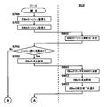
- FIG. 7 shows an example of the second embodiment of the data rewriting process for rewriting data in the flash ROM 130 of the ECU 100.
- the operator designates rewriting data and rewritten data and performs a predetermined operation on the tool 300. Executed.
- processes that are the same as those in the first embodiment are simplified from the viewpoint of eliminating redundant description (the same applies hereinafter).
- step 300 the processor 310 of the tool 300 requests the ECU 100 to erase the data in the erase block EBx in the flash ROM 130.
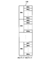
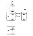
- step 400 in response to the erase request from the tool 300, the processor 110 of the ECU 100 saves the data of the write block WBy written in the erase block EBx of the flash ROM 130 in the RAM 140 as shown in FIG. make a copy.
- step 401 the processor 110 of the ECU 100 erases the data of the erase block EBx in the flash ROM 130.
- the processor 110 of the ECU 100 notifies the tool 300 that data erasure of the erase block EBx in the flash ROM 130 has been completed.
- step 301 the processor 310 of the tool 300 sequentially calculates the hash value of the data of each write block WBy belonging to the erasure block EBx of the rewrite data using a known hash function. Then, the processor 310 temporarily stores the hash value calculated from the data of the writing block WBy in the storage medium.
- step 302 the processor 310 of the tool 300 designates, for example, the address of the writing block WBy to the ECU 100, so that the hash value of the data of the writing block WBy in the rewritten data written in the flash ROM 130 is obtained. Request.
- step 403 in response to the hash value request from the tool 300, the processor 110 of the ECU 100 calculates the hash value of the data in the writing block WBy starting from the designated address of the rewritten data written in the flash ROM 130. .
- the processor 110 calculates a hash value by using the same hash function as that of the tool 300 so that the tool 300 can compare hash values. Then, the processor 110 returns the hash value calculated from the writing block WBy to the tool 300.
- step 303 the processor 310 of the tool 300 determines whether there is a difference between the two hash values by comparing the hash value stored in the storage medium with the hash value returned from the ECU 100. That is, the processor 310 determines whether or not there is a difference in the data of the corresponding writing block between the rewritten data and the rewritten data, in other words, whether or not there is identity. If the processor 310 determines that there is a difference between the two hash values, the process proceeds to step 304 (Yes). If the processor 310 determines that there is no difference between the two hash values, the process proceeds to step 305 ( No).
- step 304 the processor 310 of the tool 300 sequentially extracts the data of the writing block WBy from the rewritten data and transmits it to the ECU 100.
- step 404 the processor 110 of the ECU 100 writes the data received from the tool 300 into the write block WBy of the flash ROM 130. Thereafter, the processor 110 advances the process to step 406.
- step 305 the processor 310 of the tool 300 requests the ECU 100 to write the data of the write block WBy to the write block WBy of the flash ROM 130 for the erase block EBx data saved in the RAM 140.
- step 405 in response to the write request from the tool 300, the processor 110 of the ECU 100 writes the data of the write block WBy into the write block WBy of the flash ROM 130 for the erase block EBx data saved in the RAM 140. .
- step 406 the processor 110 of the ECU 100 notifies the tool 300 that the writing of the data in the writing block WBy has been completed.
- step 306 in response to the notification from the ECU 100, for example, whether or not the data writing to the erasure block EBx is completed through whether or not the processing up to the writing block WBm is performed by the processor 310 of the tool 300. judge. Then, the processor 310 terminates the processing of the erase block EBx if it is determined that the data writing is completed (Yes), and returns the processing to step 301 if it is determined that the data writing is not completed (No).
- the ECU 100 in response to the erase request from the tool 300, erases the data of the erase block EBx after saving the data of the erase block EBx of the flash ROM 300 to the RAM 140. To do. Thereafter, it is determined whether or not there is a difference between the writing block WBy of the rewritten data and the writing block WBy of the rewritten data, using a hash value that can evaluate the identity of the data. If there is a difference between the rewritten data and the rewritten data, the data of the writing block WBy transmitted from the tool 300 to the ECU 100 is written in the flash ROM 130. On the other hand, if there is no difference between the rewritten data and the rewritten data, the data of the writing block WBy saved in the RAM 140 is written in the flash ROM 130.
- the data transmitted / received between the tool 300 and the ECU 100 is only the write data WBy that is different between the rewritten data and the rewritten data except for various requests and responses. For this reason, compared to the first embodiment, the total amount of data transmitted from the tool 300 to the ECU 100 is further reduced, and the time required for data rewriting of the flash ROM 130 is further shortened by further shortening the data transfer time. be able to.
- the sum of the time required to save data from flash ROM 130 to RAM 140 and the time required to write data in RAM 140 to flash ROM 130 is the time required to transmit data of the same size from tool 300 to ECU 100. Shorter than. This is because the data transfer speed inside the ECU 100 is faster than the data transfer speed from the tool 300 to the ECU 100. For this reason, even if requests and responses transmitted / received between the tool 300 and the ECU 100 increase somewhat, the data transmitted from the tool 300 to the ECU 100 decreases, so that the flash ROM 130 is compared with the first embodiment. The time required for data rewriting becomes shorter.
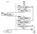
- FIG. 9 shows an example of the third embodiment of the data rewriting process for rewriting data in the flash ROM 130 of the ECU 100.
- the operator designates rewriting data and rewritten data and performs a predetermined operation on the tool 300. Executed.
- the storage 330 of the tool 300 stores a record for specifying whether or not there is a difference between the rewritten data and the rewritten data for each erase block EBx.
- Database has been built.
- a record for specifying whether or not there is a difference between the rewritten data and the rewritten data may be stored for each writing block WBy.
- step 500 the processor 310 of the tool 300 requests the ECU 100 for data identification information for identifying rewritten data.
- the processor 110 of the ECU 100 reads data identification information from the rewritten data written in the flash ROM 130, for example, and returns it to the tool 300.
- step 501 the processor 310 of the tool 300 identifies rewritten data written in the flash ROM 130 of the ECU 100 based on the data identification information returned from the ECU 100.
- the processor 310 of the tool 300 refers to the database of the storage 330 and calculates difference information between the rewritten data and the rewritten data, that is, information for specifying which erase block EBx is different. . Specifically, the processor 310 refers to the database and searches for a record specified by the data identification information of the rewritten data and the identification information of the rewritten data. Then, the processor 310 reads the contents of the record and compares the erase block EBx corresponding to the rewritten data and the rewritten data, thereby generating difference information.
- step 503 the processor 310 of the tool 300 sequentially requests the ECU 100 to erase the data of the erase block EBx of the flash ROM 130 for the erase block EBx having a difference between the rewritten data and the rewritten data.
- step 601 the processor 110 of the ECU 100 erases the data in the erase block EBx of the flash ROM 130 in response to the erase request from the tool 300.
- step 602 the processor 110 of the ECU 100 notifies the tool 300 that data erasure of the erase block EBx of the flash ROM 130 has been completed.
- step 504 in response to the notification from the ECU 100, the processor 310 of the tool 300 sequentially extracts the data of the write block WBy belonging to the erase block EBx from the write data, and transmits this to the ECU 100.
- step 603 the processor 110 of the ECU 100 writes the data received from the tool 300 into the writing block WBy of the flash ROM 130.
- step 604 the processor 110 of the ECU 100 notifies the tool 300 that the data writing to the writing block WBy of the flash ROM 130 has been completed.
- step 505 in response to the notification from the ECU 100, the processor 310 of the tool 300 determines whether or not the writing of data to the erase block EBx is completed. If the processor 310 determines that the data writing has been completed, the process proceeds to step 506 (Yes), whereas if the processor 310 determines that the data writing has not ended, the process returns to step 504 (No).
- step 506 whether or not writing of all the differences is completed through whether or not the processor 310 of the tool 300 has processed all the erase blocks EBx that are different between the rewritten data and the rewritten data. Determine whether. If the processor 310 determines that all the differences have been written, the processor 310 ends the data rewriting process (Yes), while if it determines that all the differences have not been written, the processor 310 returns the processing to step 503. (No).
- the tool 300 refers to the database of the storage 330 and calculates difference information between the rewritten data and the rewritten data.
- the erase block EBx specified by the difference information and having a difference between the rewritten data and the rewritten data the data erase of the erase block EBx of the flash ROM 130 and the write block WBy from the tool 300 to the ECU 100 Data transfer is performed. Therefore, unlike the first and second embodiments, it is not necessary to calculate a hash value in order to evaluate the identity between the rewritten data and the rewritten data, and the flash ROM 130 is more than the second embodiment. The time required for rewriting data can be shortened.
- the data of the erase block EBx is saved in the RAM 140 as in the second embodiment, and there is a difference between the tool 300 and the ECU 100. Only the data of the embedded block WBy may be transmitted to rewrite the data of the flash ROM 130. In this case, it is necessary to store in the database of the storage 330 of the tool 300 a record for specifying whether or not there is a difference between the rewritten data and the rewritten data for each writing block WBy. There is.
- the data rewriting process is mainly performed by the tool 300, but the ECU 100 may be mainly performed. Specific examples thereof will be described below.
- FIG. 10 and FIG. 11 show an example of the first applied embodiment of the data rewriting process in which the technical ideas of the first embodiment and the second embodiment are combined.
- the tool 300 is the main data rewriting process.
- step 700 the processor 310 of the tool 300 calculates the hash value of the data of the erase block EBx in the rewritten data.
- step 701 the processor 310 of the tool 300 requests the ECU 100 for a hash value of the data of the erase block EBx in the rewritten data.
- step 800 the processor 110 of the ECU 100 calculates the hash value of the data of the erase block EBx in the rewritten data in response to the request for the hash value from the tool 300. Then, the processor 110 returns the hash value calculated from the erase block EBx to the tool 300.
- step 702 the processor 310 of the tool 300 determines whether or not there is a difference between the hash value of the rewritten data and the hash value of the rewritten data for the corresponding erase block EBx. If it is determined that there is a difference between the two hash values, the processor 310 advances the process to step 703 (Yes). If it is determined that there is no difference between the two hash values, the processor 310 ends the process of the erase block EBx. (No).
- step 703 the processor 310 of the tool 300 requests the ECU 100 to erase the data in the erase block EBx in the flash ROM 130.
- step 801 the processor 110 of the ECU 100 saves the data written in the erase block EBx of the flash ROM 130 in the RAM 140 in response to the erase request from the tool 300.
- step 802 the processor 110 of the ECU 100 erases the data of the erase block EBx in the flash ROM 130.
- the processor 110 of the ECU 100 notifies the tool 300 that data erasure of the erase block EBx in the flash ROM 130 has been completed.
- step 704 the processor 310 of the tool 300 sequentially calculates the hash value of the data of each write block WBy belonging to the erasure block EBx of the rewrite data using a known hash function.
- step 705 the processor 310 of the tool 300 requests the ECU 100 for a hash value of the data of the writing block WBy in the rewritten data.
- step 804 in response to the hash value request from the tool 300, the processor 110 of the ECU 100 calculates the hash value of the data of the writing block WBy in the rewritten data. Then, the processor 110 returns the hash value calculated from the writing block WBy to the tool 300.
- step 706 the processor 310 of the tool 300 determines whether or not there is a difference between the hash value of the rewritten data and the hash value of the rewritten data for the corresponding writing block WBy. If the processor 310 determines that there is a difference between the two hash values, the process proceeds to step 707 (Yes). If the processor 310 determines that there is no difference between the two hash values, the process proceeds to step 708 (step 708). No).
- step 707 the processor 310 of the tool 300 sequentially extracts the data of the writing block WBy from the rewritten data and transmits it to the ECU 100.
- step 805 the processor 110 of the ECU 100 writes the data received from the tool 300 into the writing block WBy of the flash ROM 130. Thereafter, the processor 110 advances the processing to step 807.
- step 708 the processor 310 of the tool 300 requests the ECU 100 to write the data of the write block WBy to the write block WBy of the flash ROM 130 with respect to the data of the erase block EBx saved in the ROM 140.
- step 806 in response to the write request from the tool 300, the processor 110 of the ECU 100 writes the data of the write block WBy to the write block WBy of the flash ROM 130 for the erase block EBx data saved in the RAM 140. .
- step 807 the processor 110 of the ECU 100 notifies the tool 300 that the writing of the data in the writing block WBy has been completed.
- step 709 in response to the notification from the ECU 100, the processor 310 of the tool 300 determines whether or not data writing to the erase block EBx is completed. Then, the processor 310 terminates the processing of the erase block EBx if it is determined that the data writing has been completed (Yes), and returns the processing to step 704 if it determines that the data writing has not been completed (No).
- the identity of each writing block is evaluated with respect to the erase block having a difference between the rewriting data and the rewritten data. If the corresponding writing block is identical, the data saved in the RAM 140 is written in the flash ROM 130. If the corresponding writing block is not identical, the data transmitted from the tool 300 to the ECU 100 is flashed. It is written in the ROM 130.
- the total amount of data transmitted from the tool 300 to the ECU 100 is further reduced, and the time required for writing data in the flash ROM 130 can be shortened.
- FIG. 12 and FIG. 13 show an example of a second applied embodiment of the data rewriting process that combines the technical ideas of the first embodiment and the second embodiment.
- the main body of the data rewriting process is the ECU 100.
- step 900 the processor 310 of the tool 300 calculates the hash value of the data of the erase block EBx in the rewritten data.
- step 901 the processor 310 of the tool 300 requests the ECU 100 to erase the erase block EBx in the rewritten data, and transmits the hash value calculated in step 900.
- step 1000 the processor 110 of the ECU 100 calculates the hash value of the data of the erase block EBx in the rewritten data in response to the erase request from the tool 300.
- step 1001 the processor 110 of the ECU 100 compares the hash value received from the tool 300 with the hash value calculated in step 1000 to determine whether there is a difference between the two hash values. If it is determined that there is a difference between the two hash values, the processor 110 proceeds to step 1002 (Yes), and if it is determined that there is no difference between the two hash values, the processing of the erase block EBx is terminated. (No).
- step 1002 the processor 110 of the ECU 100 saves the data written in the erase block EBx of the flash ROM 130 in the RAM 140.
- step 1003 the processor 110 of the ECU 100 erases the data of the erase block EBx in the flash ROM 130.
- step 1004 the processor 110 of the ECU 100 sequentially calculates the hash value of the data of the write block WBy from the data of the erase block EBx saved in the RAM 140.
- step 1005 the processor 110 of the ECU 100 requests the hash value of the data of the write block WBy belonging to the erasure block EBx of the rewrite data to the tool 300.
- step 902 the processor 310 of the tool 300 calculates the hash value of the data of the writing block WBy in the rewritten data in response to the hash value request from the ECU 100. Then, the processor 310 returns the hash value calculated from the writing block WBy to the ECU 100.
- step 1006 the processor 110 of the ECU 100 determines whether or not there is a difference between the hash value of the rewritten data and the hash value of the rewritten data for the corresponding writing block WBy. If the processor 110 determines that there is a difference between the two hash values, the process proceeds to step 1007 (Yes). If the processor 110 determines that there is no difference between the two hash values, the process proceeds to step 1009 ( No).
- step 1007 the processor 110 of the ECU 100 requests the data of the writing block WBy in the rewriting data from the tool 300.
- step 903 in response to a request from the ECU 100, the processor 310 of the tool 300 sequentially extracts the data of the writing block WBy from the rewritten data, and transmits this to the ECU 100.
- step 1008 the processor 110 of the ECU 100 writes the data received from the tool 300 into the writing block WBy of the flash ROM 130. After that, the processor 110 advances the process to step 1010.
- step 1009 the processor 110 of the ECU 100 writes the data of the write block WBy into the write block WBy of the flash ROM 130 with respect to the data of the erase block EBx saved in the RAM 140.
- step 1010 the processor 110 of the ECU 100 determines whether or not the data writing to the erase block EBx is completed. If the processor 110 determines that the data writing has been completed, the processor 110 terminates the processing of the erase block EBx (Yes), and if it determines that the data writing has not ended, returns the processing to step 1004 (No).
- the data writing process is performed in the ECU 100 except for the basic erase request of the erase block EBx, the return of the hash value of the write block WBy, and the transmission of the write block WBy. .
- the processing in the tool 300 also needs to be changed. Since there is little influence, the change part can be decreased. Since the tool 300 is commonly used for various ECUs 100, such an effect is useful. Since other operations and effects are the same as those of the first applied embodiment, refer to the description if necessary.
- a data rewriting system can be constructed.
- hash values of the data of the erase block EBx and the write block WBy are calculated in advance and stored in association with the rewrite data and the rewritten data. Good. In this way, when the data in the flash ROM 130 is rewritten, the process of calculating the hash value is not necessary, and the load on the tool 300 and the ECU 100 can be reduced.
- the data writing process of the ECU 100 to the flash ROM 130 may be performed while the ECU 100 is mounted on the vehicle. In this way, for example, even if the control program is changed due to function expansion or the like, the data of the ECU 100 mounted on the vehicle can be rewritten.
- ECU 110 processor 120 communication circuit 130 flash ROM (nonvolatile memory) 140 RAM (volatile memory) 200 Network cable 300 Tool 310 Processor 320 Communication circuit
Landscapes
- Engineering & Computer Science (AREA)
- Theoretical Computer Science (AREA)
- Physics & Mathematics (AREA)
- General Engineering & Computer Science (AREA)
- General Physics & Mathematics (AREA)
- Human Computer Interaction (AREA)
- Automation & Control Theory (AREA)
- Stored Programmes (AREA)
- Read Only Memory (AREA)
- Memory System (AREA)
Abstract
Description
図1は、自動車に搭載される電子制御装置(ECU:Electronic Control Unit)のデータを書き換える、データ書換えシステムの一例を示す。
ステップ204では、ECU100のプロセッサ110が、ツール300に対して、フラッシュROM130の書込ブロックWByへのデータ書き込みが終了したことを通知する。
ステップ400では、ECU100のプロセッサ110が、ツール300からの消去要求に応答して、図8に示すように、フラッシュROM130の消去ブロックEBxに書き込まれている書込ブロックWByのデータをRAM140に退避(コピー)する。
ステップ402では、ECU100のプロセッサ110が、ツール300に対して、フラッシュROM130における消去ブロックEBxのデータ消去が終了したことを通知する。
ステップ404では、ECU100のプロセッサ110が、ツール300から受信したデータをフラッシュROM130の書込ブロックWByに書き込む。その後、プロセッサ110は、処理をステップ406へと進める。
ステップ306では、ツール300のプロセッサ310が、ECU100からの通知に応答して、例えば、書込ブロックWBmまで処理したか否かを介して、消去ブロックEBxへのデータ書込みが終了したか否かを判定する。そして、プロセッサ310は、データ書込みが終了したと判定すれば消去ブロックEBxの処理を終了させる一方(Yes)、データ書込みが終了していないと判定すれば処理をステップ301へと戻す(No)。
ステップ600では、ECU100のプロセッサ110が、例えば、フラッシュROM130に書き込まれている被書換えデータからデータ識別情報を読み出し、これをツール300へと返送する。
ステップ602では、ECU100のプロセッサ110が、ツール300に対して、フラッシュROM130の消去ブロックEBxのデータ消去が終了したことを通知する。
ステップ604では、ECU100のプロセッサ110が、ツール300に対して、フラッシュROM130の書込ブロックWByへのデータ書き込みが終了したことを通知する。
ステップ701では、ツール300のプロセッサ310が、ECU100に対して、被書換えデータにおける消去ブロックEBxのデータのハッシュ値を要求する。
ステップ801では、ECU100のプロセッサ110が、ツール300からの消去要求に応答して、フラッシュROM130の消去ブロックEBxに書き込まれているデータをRAM140に退避する。
ステップ803では、ECU100のプロセッサ110が、ツール300に対して、フラッシュROM130における消去ブロックEBxのデータ消去が終了したことを通知する。
ステップ804では、ECU100のプロセッサ110が、ツール300からのハッシュ値の要求に応答して、被書換えデータにおける書込ブロックWByのデータのハッシュ値を算出する。そして、プロセッサ110は、書込ブロックWByから算出したハッシュ値をツール300に返送する。
ステップ805では、ECU100のプロセッサ110が、ツール300から受信したデータをフラッシュROM130の書込ブロックWByに書き込む。その後、プロセッサ110は、処理をステップ807へと進める。
ステップ709では、ツール300のプロセッサ310が、ECU100からの通知に応答して、消去ブロックEBxへのデータ書込みが終了したか否かを判定する。そして、プロセッサ310は、データ書込みが終了したと判定すれば消去ブロックEBxの処理を終了させる一方(Yes)、データ書込みが終了していないと判定すれば処理をステップ704へと戻す(No)。
ステップ901では、ツール300のプロセッサ310が、ECU100に対して、被書換えデータにおける消去ブロックEBxのデータ消去を要求すると共に、ステップ900で算出したハッシュ値を送信する。
ステップ1003では、ECU100のプロセッサ110が、フラッシュROM130における消去ブロックEBxのデータを消去する。
ステップ1005では、ECU100のプロセッサ110が、ツール300に対して、書換えデータの消去ブロックEBxに属する書込ブロックWByのデータのハッシュ値を要求する。
ステップ903では、ツール300のプロセッサ310が、ECU100からの要求に応答して、書換えデータから書込ブロックWByのデータを順次抽出し、これをECU100に対して送信する。
110 プロセッサ
120 通信回路
130 フラッシュROM(不揮発性メモリ)
140 RAM(揮発性メモリ)
200 ネットワークケーブル
300 ツール
310 プロセッサ
320 通信回路
Claims (14)
- 消去ブロック単位でデータを消去可能であると共に、前記消去ブロックよりも小さい書込ブロック単位でデータを書込み可能な不揮発性メモリと、プロセッサと、を有する電子制御装置であって、
前記プロセッサが、外部からのデータ書換え要求に応答して、前記不揮発性メモリの一部のデータを消去ブロック単位で消去し、前記不揮発性メモリの一部に書込ブロック単位でデータを書き込むように構成された、
ことを特徴とする電子制御装置。 - 前記プロセッサが、前記消去ブロック単位で、前記不揮発性メモリに書き込むデータの識別情報と、前記不揮発性メモリに書き込まれているデータの識別情報と、の同一性を判定し、前記同一性がないと判定された消去ブロックについて、データの消去及び書込みを実行するように構成された、
ことを特徴とする請求項1に記載の電子制御装置。 - 前記データの識別情報は、ハッシュ値である、
ことを特徴とする請求項2に記載の電子制御装置。 - 前記プロセッサが、
前記消去ブロック単位で、前記不揮発性メモリに書き込まれているデータを揮発性メモリに退避してから消去し、
前記書込ブロック単位で、前記不揮発性メモリに書き込むデータの識別情報と、前記揮発性メモリに退避されたデータの識別情報と、の同一性を判定し、
前記同一性がある場合、前記揮発性メモリに退避されたデータを前記不揮発性メモリに書き込む一方、前記同一性がない場合、外部からのデータを前記不揮発性メモリに書き込むように構成された、
ことを特徴とする請求項1に記載の電子制御装置。 - 前記データの識別情報は、ハッシュ値である、
ことを特徴とする請求項4に記載の電子制御装置。 - 前記電子制御装置に対して接続され、プロセッサを有するツールを更に含み、
前記ツールのプロセッサは、前記不揮発性メモリに書き込むデータと前記不揮発性メモリに書き込まれているデータとの差分情報に基づいて、前記電子制御装置にデータ書換え要求を送信するように構成された、
ことを特徴とする請求項1に記載の電子制御装置。 - 前記ツールのプロセッサは、前記不揮発性メモリに書き込むデータと前記不揮発性メモリに書き込まれているデータとの間で同一性がない消去ブロック単位のデータについて、前記電子制御装置にデータ書換え要求を送信するように構成された、
ことを特徴とする請求項6に記載の電子制御装置。 - 前記ツールのプロセッサは、前記不揮発性メモリに書き込むデータと前記不揮発性メモリに書き込まれているデータとの差分情報が格納されたデータベースを参照し、前記電子制御装置から送信されたデータの識別情報に応じた差分情報を求めるように構成された、
ことを特徴とする請求項6に記載の電子制御装置。 - 消去ブロック単位でデータを消去可能であると共に、前記消去ブロックよりも小さい書込ブロック単位でデータを書込み可能な不揮発性メモリを有する電子制御装置のプロセッサが、
外部からのデータ書換え要求に応答して、前記不揮発性メモリの一部のデータを消去ブロック単位で消去し、
前記不揮発性メモリの一部に書込ブロック単位でデータを書き込む、
ことを特徴とするデータ書換え方法。 - 前記電子制御装置のプロセッサが、
前記消去ブロック単位で、前記不揮発性メモリに書き込むデータの識別情報と、前記不揮発性メモリに書き込まれているデータの識別情報と、の同一性を判定し、
前記同一性がないと判定した消去ブロックについて、データの消去及び書き込みを実行する、
ことを特徴とする請求項9に記載のデータ書換え方法。 - 前記電子制御装置のプロセッサが、
前記消去ブロック単位で、前記不揮発性メモリに書き込まれているデータを揮発性メモリに退避してから消去し、
前記書込ブロック単位で、前記不揮発性メモリに書き込むデータの識別情報と、前記揮発性メモリに退避されたデータの識別情報と、の同一性を判定し、
前記同一性がある場合、前記揮発性メモリに退避されたデータを前記不揮発性メモリに書き込む一方、前記同一性がない場合、外部からのデータを前記不揮発性メモリに書き込む、
ことを特徴とする請求項9に記載のデータ書換え方法。 - 前記電子制御装置に対して接続されるツールのプロセッサが、
前記不揮発性メモリに書き込むデータと前記不揮発性メモリに書き込まれているデータとの差分情報に基づいて、前記電子制御装置にデータ書換え要求を送信する、
ことを特徴とする請求項9に記載のデータ書換え方法。 - 前記ツールのプロセッサが、
前記不揮発性メモリに書き込むデータと前記不揮発性メモリに書き込まれているデータとの間で同一性がない消去ブロック単位のデータについて、前記電子制御装置にデータ書換え要求を送信する、
ことを特徴とする請求項12に記載のデータ書換え方法。 - 前記ツールのプロセッサが、
前記不揮発性メモリに書き込むデータと前記不揮発性メモリに書き込まれているデータとの差分情報が格納されたデータベースを参照し、前記電子制御装置から送信されたデータの識別情報に応じた差分情報を求める、
ことを特徴とする請求項12に記載のデータ書換え方法。
Priority Applications (4)
| Application Number | Priority Date | Filing Date | Title |
|---|---|---|---|
| CN201480016490.2A CN105144299B (zh) | 2013-03-21 | 2014-02-25 | 电子控制装置以及数据改写方法 |
| GB1516785.1A GB2526992B (en) | 2013-03-21 | 2014-02-25 | Electronic control unit and method for rewriting data |
| US14/778,896 US9996296B2 (en) | 2013-03-21 | 2014-02-25 | Electronic control unit and method for rewriting data |
| MX2015012412A MX361290B (es) | 2013-03-21 | 2014-02-25 | Unidad de control electrónico y método para reescribir datos. |
Applications Claiming Priority (2)
| Application Number | Priority Date | Filing Date | Title |
|---|---|---|---|
| JP2013-058175 | 2013-03-21 | ||
| JP2013058175A JP6030485B2 (ja) | 2013-03-21 | 2013-03-21 | 電子制御装置 |
Publications (1)
| Publication Number | Publication Date |
|---|---|
| WO2014148208A1 true WO2014148208A1 (ja) | 2014-09-25 |
Family
ID=51579900
Family Applications (1)
| Application Number | Title | Priority Date | Filing Date |
|---|---|---|---|
| PCT/JP2014/054484 Ceased WO2014148208A1 (ja) | 2013-03-21 | 2014-02-25 | 電子制御装置及びデータ書換え方法 |
Country Status (6)
| Country | Link |
|---|---|
| US (1) | US9996296B2 (ja) |
| JP (1) | JP6030485B2 (ja) |
| CN (1) | CN105144299B (ja) |
| GB (1) | GB2526992B (ja) |
| MX (1) | MX361290B (ja) |
| WO (1) | WO2014148208A1 (ja) |
Families Citing this family (4)
| Publication number | Priority date | Publication date | Assignee | Title |
|---|---|---|---|---|
| JP6308074B2 (ja) * | 2014-08-27 | 2018-04-11 | 株式会社デンソー | マイクロコンピュータ |
| JP6699324B2 (ja) | 2016-04-26 | 2020-05-27 | 株式会社デンソー | 電子制御装置及びデータ書換えシステム |
| JP6913621B2 (ja) * | 2017-12-19 | 2021-08-04 | 日立Astemo株式会社 | 自動車用電子制御装置 |
| JP2021043843A (ja) * | 2019-09-13 | 2021-03-18 | 日立オートモティブシステムズ株式会社 | 転送装置、電子制御装置及びこれを製造する方法 |
Citations (5)
| Publication number | Priority date | Publication date | Assignee | Title |
|---|---|---|---|---|
| JPH06162786A (ja) * | 1992-11-18 | 1994-06-10 | Hitachi Ltd | フラッシュメモリを用いた情報処理装置 |
| JPH08202626A (ja) * | 1995-01-31 | 1996-08-09 | Isuzu Motors Ltd | メモリ制御装置 |
| JP2003131898A (ja) * | 2001-10-24 | 2003-05-09 | Sharp Corp | 電子機器、及びフラッシュメモリの書き換えシステム |
| JP2009252294A (ja) * | 2008-04-07 | 2009-10-29 | Spansion Llc | メモリコントローラ、メモリシステム、及びメモリデバイスへのデータの書込方法 |
| JP2010009164A (ja) * | 2008-06-25 | 2010-01-14 | Kyocera Mita Corp | 記録装置、画像形成装置、及びオプション装置 |
Family Cites Families (12)
| Publication number | Priority date | Publication date | Assignee | Title |
|---|---|---|---|---|
| JPH08315596A (ja) * | 1995-05-12 | 1996-11-29 | Nec Corp | 半導体記憶装置 |
| JPH09128229A (ja) | 1995-11-06 | 1997-05-16 | Denso Corp | 電子制御装置 |
| JPH11141391A (ja) * | 1997-11-06 | 1999-05-25 | Hitachi Ltd | 自動車用制御装置 |
| JP2000192844A (ja) * | 1998-12-25 | 2000-07-11 | Hitachi Ltd | エンジン制御装置 |
| JP2002014833A (ja) * | 2000-06-30 | 2002-01-18 | Konica Corp | フラッシュメモリの書き換え方式、制御装置、画像形成装置及びプログラム更新方式 |
| JP2003272389A (ja) * | 2002-03-20 | 2003-09-26 | Sony Corp | データ記憶回路及び同データ記憶回路におけるデータ書込み方法及びデータ記憶装置 |
| US20080132204A1 (en) * | 2006-12-04 | 2008-06-05 | Motorola, Inc. | System and method for updating at least one attribute stored at a mobile station |
| US8219781B2 (en) * | 2008-11-06 | 2012-07-10 | Silicon Motion Inc. | Method for managing a memory apparatus, and associated memory apparatus thereof |
| US8769188B2 (en) * | 2009-11-18 | 2014-07-01 | Mediatek Inc. | Nonvolatile memory controller and method for writing data to nonvolatile memory |
| US8406059B2 (en) * | 2009-12-24 | 2013-03-26 | Samsung Electronics Co., Ltd. | Nonvolatile semiconductor memory devices, data updating methods thereof, and nonvolatile semiconductor memory systems |
| EP2653970A4 (en) * | 2010-12-15 | 2014-01-29 | Fujitsu Ltd | DATA TRANSFER PROGRAM, COMPUTERS AND DATA TRANSMISSION PROCEDURES |
| US9032137B2 (en) * | 2012-11-21 | 2015-05-12 | Intel Corporation | Flexible wear management for non-volatile memory |
-
2013
- 2013-03-21 JP JP2013058175A patent/JP6030485B2/ja active Active
-
2014
- 2014-02-25 GB GB1516785.1A patent/GB2526992B/en active Active
- 2014-02-25 MX MX2015012412A patent/MX361290B/es active IP Right Grant
- 2014-02-25 CN CN201480016490.2A patent/CN105144299B/zh active Active
- 2014-02-25 WO PCT/JP2014/054484 patent/WO2014148208A1/ja not_active Ceased
- 2014-02-25 US US14/778,896 patent/US9996296B2/en active Active
Patent Citations (5)
| Publication number | Priority date | Publication date | Assignee | Title |
|---|---|---|---|---|
| JPH06162786A (ja) * | 1992-11-18 | 1994-06-10 | Hitachi Ltd | フラッシュメモリを用いた情報処理装置 |
| JPH08202626A (ja) * | 1995-01-31 | 1996-08-09 | Isuzu Motors Ltd | メモリ制御装置 |
| JP2003131898A (ja) * | 2001-10-24 | 2003-05-09 | Sharp Corp | 電子機器、及びフラッシュメモリの書き換えシステム |
| JP2009252294A (ja) * | 2008-04-07 | 2009-10-29 | Spansion Llc | メモリコントローラ、メモリシステム、及びメモリデバイスへのデータの書込方法 |
| JP2010009164A (ja) * | 2008-06-25 | 2010-01-14 | Kyocera Mita Corp | 記録装置、画像形成装置、及びオプション装置 |
Also Published As
| Publication number | Publication date |
|---|---|
| CN105144299B (zh) | 2021-01-12 |
| GB2526992A (en) | 2015-12-09 |
| CN105144299A (zh) | 2015-12-09 |
| GB201516785D0 (en) | 2015-11-04 |
| MX361290B (es) | 2018-12-03 |
| JP2014182859A (ja) | 2014-09-29 |
| MX2015012412A (es) | 2016-07-15 |
| GB2526992B (en) | 2020-05-06 |
| US20160048336A1 (en) | 2016-02-18 |
| US9996296B2 (en) | 2018-06-12 |
| JP6030485B2 (ja) | 2016-11-24 |
Similar Documents
| Publication | Publication Date | Title |
|---|---|---|
| KR102567097B1 (ko) | 임베디드 시스템의 부트 롬 업데이트 방법 및 부팅 방법 | |
| US9858008B2 (en) | Method to reduce flash memory IOs with host maintained address mapping table | |
| US11681463B2 (en) | Offload defrag operation for host-managed storage | |
| US20190391761A1 (en) | Storage device with a callback response | |
| CN105701021A (zh) | 数据储存装置及其数据写入方法 | |
| US11360698B2 (en) | Electronic control unit for vehicle and method of writing data | |
| JP6030485B2 (ja) | 電子制御装置 | |
| JP6913621B2 (ja) | 自動車用電子制御装置 | |
| CN103890731A (zh) | 汽车用电子控制装置以及数据通信方法 | |
| JP2011175632A (ja) | 半導体記憶装置及び半導体記憶装置の制御方法 | |
| KR20170139730A (ko) | 데이터 저장 장치 및 그것의 동작 방법 | |
| JP2016170471A (ja) | 電子制御装置 | |
| US20140219041A1 (en) | Storage device and data processing method thereof | |
| US20170220252A1 (en) | Flash emulated eeprom wrapper | |
| US20170200503A1 (en) | Storage apparatus, flash memory control apparatus, and program | |
| JP2012027806A (ja) | メモリ管理装置およびメモリ管理方法 | |
| US20250190337A1 (en) | Electronic control device and write control method | |
| JP4973844B2 (ja) | オブジェクト指向型車両用制御装置 | |
| JP5180726B2 (ja) | 記憶装置およびデータ書き込み制御方法 | |
| JP5787095B2 (ja) | 不揮発性メモリへのデータ記憶方法 | |
| US11698732B2 (en) | Storage provisioning in a data storage device | |
| JP5332800B2 (ja) | 記憶装置 | |
| CN103942504B (zh) | 可携式储存装置及其数据安全控制方法 | |
| CN115658155A (zh) | 一种新能源汽车整车控制器双系统切换的方法及系统 | |
| CN121900780A (zh) | 一种车辆的软件刷写方法、终端设备、车辆及存储介质 |
Legal Events
| Date | Code | Title | Description |
|---|---|---|---|
| WWE | Wipo information: entry into national phase |
Ref document number: 201480016490.2 Country of ref document: CN |
|
| 121 | Ep: the epo has been informed by wipo that ep was designated in this application |
Ref document number: 14768514 Country of ref document: EP Kind code of ref document: A1 |
|
| DPE1 | Request for preliminary examination filed after expiration of 19th month from priority date (pct application filed from 20040101) | ||
| WWE | Wipo information: entry into national phase |
Ref document number: MX/A/2015/012412 Country of ref document: MX |
|
| NENP | Non-entry into the national phase |
Ref country code: DE |
|
| WWE | Wipo information: entry into national phase |
Ref document number: 14778896 Country of ref document: US |
|
| ENP | Entry into the national phase |
Ref document number: 1516785 Country of ref document: GB Kind code of ref document: A Free format text: PCT FILING DATE = 20140225 |
|
| WWE | Wipo information: entry into national phase |
Ref document number: 1516785.1 Country of ref document: GB |
|
| 122 | Ep: pct application non-entry in european phase |
Ref document number: 14768514 Country of ref document: EP Kind code of ref document: A1 |