WO2014141702A1 - Organic light emitting device (oled) and method for fabricating oled - Google Patents
Organic light emitting device (oled) and method for fabricating oled Download PDFInfo
- Publication number
- WO2014141702A1 WO2014141702A1 PCT/JP2014/001405 JP2014001405W WO2014141702A1 WO 2014141702 A1 WO2014141702 A1 WO 2014141702A1 JP 2014001405 W JP2014001405 W JP 2014001405W WO 2014141702 A1 WO2014141702 A1 WO 2014141702A1
- Authority
- WO
- WIPO (PCT)
- Prior art keywords
- layer
- oled
- back mirror
- spherical
- light
- Prior art date
- Legal status (The legal status is an assumption and is not a legal conclusion. Google has not performed a legal analysis and makes no representation as to the accuracy of the status listed.)
- Ceased
Links
Images








Classifications
-
- H—ELECTRICITY
- H10—SEMICONDUCTOR DEVICES; ELECTRIC SOLID-STATE DEVICES NOT OTHERWISE PROVIDED FOR
- H10K—ORGANIC ELECTRIC SOLID-STATE DEVICES
- H10K77/00—Constructional details of devices covered by this subclass and not covered by groups H10K10/80, H10K30/80, H10K50/80 or H10K59/80
- H10K77/10—Substrates, e.g. flexible substrates
-
- H—ELECTRICITY
- H10—SEMICONDUCTOR DEVICES; ELECTRIC SOLID-STATE DEVICES NOT OTHERWISE PROVIDED FOR
- H10K—ORGANIC ELECTRIC SOLID-STATE DEVICES
- H10K50/00—Organic light-emitting devices
- H10K50/80—Constructional details
- H10K50/85—Arrangements for extracting light from the devices
- H10K50/856—Arrangements for extracting light from the devices comprising reflective means
-
- Y—GENERAL TAGGING OF NEW TECHNOLOGICAL DEVELOPMENTS; GENERAL TAGGING OF CROSS-SECTIONAL TECHNOLOGIES SPANNING OVER SEVERAL SECTIONS OF THE IPC; TECHNICAL SUBJECTS COVERED BY FORMER USPC CROSS-REFERENCE ART COLLECTIONS [XRACs] AND DIGESTS
- Y02—TECHNOLOGIES OR APPLICATIONS FOR MITIGATION OR ADAPTATION AGAINST CLIMATE CHANGE
- Y02E—REDUCTION OF GREENHOUSE GAS [GHG] EMISSIONS, RELATED TO ENERGY GENERATION, TRANSMISSION OR DISTRIBUTION
- Y02E10/00—Energy generation through renewable energy sources
- Y02E10/50—Photovoltaic [PV] energy
- Y02E10/549—Organic PV cells
-
- Y—GENERAL TAGGING OF NEW TECHNOLOGICAL DEVELOPMENTS; GENERAL TAGGING OF CROSS-SECTIONAL TECHNOLOGIES SPANNING OVER SEVERAL SECTIONS OF THE IPC; TECHNICAL SUBJECTS COVERED BY FORMER USPC CROSS-REFERENCE ART COLLECTIONS [XRACs] AND DIGESTS
- Y02—TECHNOLOGIES OR APPLICATIONS FOR MITIGATION OR ADAPTATION AGAINST CLIMATE CHANGE
- Y02P—CLIMATE CHANGE MITIGATION TECHNOLOGIES IN THE PRODUCTION OR PROCESSING OF GOODS
- Y02P70/00—Climate change mitigation technologies in the production process for final industrial or consumer products
- Y02P70/50—Manufacturing or production processes characterised by the final manufactured product
Definitions
- This invention generally relates to organic light emitting devices (OLEDs) and, more particularly, to an OLED with a spherical back mirror for improved light extraction.
- OLEDs organic light emitting devices
- an OLED organic light-emitting diode
- the emissive electroluminescent layer is a film of organic compound which emits light in response to an electric current. This layer of organic semiconductor is situated between two electrodes. Generally, at least one of these electrodes is transparent. OLEDs are used to create digital displays in devices such as television screens, computer monitors, portable systems such as mobile phones, handheld games consoles, and PDAs.
- OLED organic light-emitting diode
- PMOLED passive-matrix
- AMOLED active-matrix OLEDs
- An OLED display works without a backlight. Thus, it can display deep black levels and can be thinner and lighter than a liquid crystal display (LCD). In low ambient light conditions such as a dark room an OLED screen can achieve a higher contrast ratio than an LCD, whether the LCD uses cold cathode fluorescent lamps or LED backlight.
- LCD liquid crystal display
- Multilayer OLEDs can be fabricated with two or more layers in order to improve device efficiency. As well as conductive properties, different materials may be chosen to aid charge injection at the electrodes by providing a more gradual electronic profile, or block a charge from reaching the opposite electrode and being wasted. Many modern OLEDs incorporate a simple bilayer structure, consisting of a conductive layer and an emissive layer.
- the emissive layer may be understood as comprising a light-emission or electron injection layer, and an electron transport layer.
- the conductive layer may be understood as comprising a hole injection layer and a hole transport layer.
- a voltage is applied across the OLED such that the anode is positive with respect to the cathode.
- a current of electrons flows through the device from cathode to anode, as electrons are injected into the lowest unoccupied molecular orbit (LUMO) of the organic layer at the cathode and withdrawn from the highest occupied molecular orbit (HOMO) at the anode.
- LUMO lowest unoccupied molecular orbit
- HOMO highest occupied molecular orbit
- the decay of this excited state results in a relaxation of the energy levels of the electron, accompanied by emission of radiation whose frequency is in the visible region.
- the frequency of this radiation depends on the band gap of the material, in this case the difference in energy between the HOMO and LUMO.
- ITO Indium tin oxide
- a typical conductive layer may consist of poly(3,4-ethylenedioxythiophene):poly(styrenesulfonate) [PEDOT:PSS] as the HOMO level of this material generally lies between the workfunction of ITO and the HOMO of other commonly used polymers, reducing the energy barriers for hole injection.
- Metals such as barium and calcium are often used for the cathode as they have low work functions which promote injection of electrons into the LUMO of the organic layer. Such metals are reactive, so they require a capping layer of aluminum to avoid degradation.
- Fig. 1 is a partial cross-sectional view of an OLED (prior art).
- Layer 1 represents a stack comprising an electron transport layer, electron injection layer, and a cathode electrode.
- layer 2 represents a stack comprising a hole transport layer, hole injection layer, and the anode electrode. Electron emission occurs at the interface between layer 1 and layer 2.
- the figure depicts energy loss in OLED structure due to the internal total reflection of high index waveguide.
- a back reflecting mirror can collected particle light and enhanced extraction efficiency. However, only the back propagation of light at can be extracted out.
- the back propagation light with is confined in the media of index and .
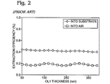
- Fig. 2 is a plot of the external extraction efficiency of the structure of Fig. 1 plotted as a function of organic layer 1 (OL1) thickness using a finite-difference time-domain simulation (prior art).
- the light source is located at the interface of organic layer 1 and organic layer 2.
- the light source is an incoherent dipole source at a wavelength of 450 nanometers (nm).
- the extraction efficiency into substrate is ⁇ 43% and that into air is close to 20% at 450 nm, with the thickness of layer 2 set to 250 nm.
- OLED organic light emitting device
- a method for fabricating an organic light emitting device (OLED) with a spherical back mirror.
- the method forms a spherical curvature in the substrate and deposits a metal film overlying the spherical curvature, forming a spherical back mirror.
- a transparent isolation layer is formed overlying the spherical back mirror having a planar top surface.
- a transparent first electrode layer is formed overlying the isolation layer, and a transparent second electrode layer is formed overlying the first electrode layer.
- a stack is interposed between the first and second electrode layers.
- the stack is made up of an electron transport layer adjacent the cathode, a light-emitting (electron injection) layer adjacent to the electron transport layer, a hole transport layer adjacent to the light-emitting layer, and a hole injection layer adjacent to the hole transport layer.
- the order of the stack layering is dependent upon which electrode is the anode and which electrode is the cathode.
- Fig. 1 is a partial cross-sectional view of an OLED (prior art).
- Fig. 2 is a plot of the external extraction efficiency of the structure of Fig. 1 plotted as a function of organic layer 1 (OL1) thickness using a finite-difference time-domain simulation (prior art).
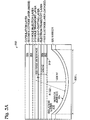
- Fig. 3A is a partial cross-sectional view of an OLED with a spherical back mirror.
- Fig. 3B is a partial cross-sectional view of an OLED with a spherical back mirror.
- Fig. 4 is a diagram depicting the reflective caustics of parallel lines upon a circular reflective surface.
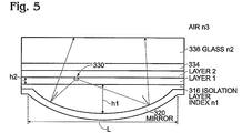
- Fig. 5 is a partial cross-sectional of the device of Fig. 3A or 3B.
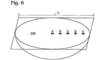
- FIG. 6 is a schematic diagram depicting a light source at five three-dimensional dipole positions along the plane of the first interface.
- Fig. 7A is a plot of extraction efficiency as a function of organic layer 1 (h2) thickness and dipole position.
- Fig. 7B is a plot of extraction efficiency as a function of organic layer 1 (h2) thickness and dipole position.
- Fig. 7C is a plot of extraction efficiency as a function of organic layer 1 (h2) thickness and dipole position.
- Fig. 7D is a plot of extraction efficiency as a function of organic layer 1 (h2) thickness and dipole position.
- Fig. 7E is a plot of extraction efficiency as a function of organic layer 1 (h2) thickness and dipole position.
- Fig. 7A is a plot of extraction efficiency as a function of organic layer 1 (h2) thickness and dipole position.
- Fig. 7B is a plot of extraction efficiency as a function of organic layer 1 (h2) thickness and dipole position.
- Fig. 7C
- Fig. 9A depicts a step in an exemplary spherical back mirror OLED fabrication process.
- Fig. 9B depicts a step in an exemplary spherical back mirror OLED fabrication process.
- Fig. 9C depicts a step in an exemplary spherical back mirror OLED fabrication process.
- Fig. 9D depicts a step in an exemplary spherical back mirror OLED fabrication process.
- Fig. 9E depicts a step in an exemplary spherical back mirror OLED fabrication process.
- Fig. 9F depicts a step in an exemplary spherical back mirror OLED fabrication process.
- Fig. 10 is a flowchart illustrating a method for fabricating an OLED with a spherical back mirror.
- Figs. 3A and 3B are partial cross-sectional views of an OLED with a spherical back mirror.
- the OLED 300 comprises a transparent first electrode layer 302 and a transparent second electrode layer 304 overlying the first electrode layer.
- An electron transport layer 306 is interposed between the first electrode layer 302 and second electrode layer 304.
- a light-emitting or electron injection layer 308 is adjacent to (i.e. in direct contact with) the electron transport layer 306.
- a hole transport layer 310 is adjacent to the light-emitting layer 308.
- a hole injection layer 312 is adjacent to the hole transport layer 310.
- a spherical back mirror concave top surface 314 underlies the first electrode layer 302.
- a transparent isolation layer 316 is interposed between the first electrode layer 302 and the spherical back mirror concave surface 314.
- the first electrode 302 is a cathode.
- the first electrode 302 is an anode.
- the first electrode layer 302 has a bottom surface 318.
- the spherical back mirror 320 has a spherical curve defined by the radius of curvature (R) 322.
- the isolation layer 316 has a thickness (h1) 326 between the center the spherical back mirror 320 and the first electrode layer bottom surface 318.
- a first interface 330 exists between the light-emission layer 308 and the hole transport layer 310, and the distance between the first interface and the first electrode layer bottom surface is h2 (332).
- (h1 + h2)/R is in the range of 0.2 to 0.4.
- the spherical curve is defined by a uniform radius of curvature (the spherical shape is circular as seen from above). Otherwise, the spherical back mirror 320 may have a non-circular shape.
- the spherical back mirror 320 has a maximum length 328 in the range of 3.6 to 176 microns. The maximum length of the spherical back mirror is driven by the value of R, which is selected for the desired size of the pixel.
- h2 is in the range of 100 to 300 nanometers (nm). It is also typical that the value of R be in the range of 3 to 110 microns, and h1 be in the range of 0.6 to 44 microns. However, it should be understood that the OLED 300 is not limited to any particular physical dimensions.
- the OLEDs are sized for use in displays. To be functional in displays, h2 must not be too thin or too thick.
- the h2 size range stated above is an example of a suitable range.
- the value for R is selected to yield OLED pixels of the desired size.
- the value range for h1 is driven by the values selected for R and h2. None of the numerical ranges stated above is absolute; they are suggested ranges for embodiments within the scope of the invention.
- the OLED 300 further comprises an inorganic capsulation layer 334 overlying the second electrode layer 304.
- the OLED further comprises both the inorganic capsulation layer 334 and a glass (or like material) layer 336 overlying the inorganic capsulation layer 334.
- the device of Fig. 3B made be made without the glass layer and the device of Fig. 3A may include a glass layer.
- the spherical back mirror 320 is a material such as Ag, Al, W, Mo, MoW, or Au. However, other highly reflective materials (e.g. with a reflectivity of greater than 90% in the visible wavelengths of light) may be used.
- the insulation layer, first electrode layer, light-emitting layer, electron transport layer, hole injection layer, hole transport layer, and second electrode layer have a refractive index of 1.75, with a tolerance of plus-minus 6%, in the visible wavelengths of light.
- the materials of the h2 layer have a relatively high index of refraction, which is why it is desirable to have relatively high refractive indices in the other adjacent layers, to match that of h2.
- Fig. 4 is a diagram depicting the reflective caustics of parallel lines upon a circular reflective surface.
- the OLEDs described above take advantage of the caustics associated with a spherical metallic surface.
- Area 400 includes a condensed ray density associated with large reflected angles.
- h1 is the distance from area 400 to the bottom of curve, and R is the radius of the curve. Because optical ray tracing is an inversible system, this system can be used for OLED design.
- the emitting layer of OLED is located within area 400, a substantial portion of the back propagation light is reflected out of the device in collimation, thereby reducing total internal reflection.
- the range of distance values for points inside area 400 is around 0.2R to 0.4R for the best OLED extraction efficiency.
- the distance to the bottom of area 400 (h1) divided by R is 0.2
- the distance to the top of area 400 divided by R is 0.4.
- Fig. 5 is a partial cross-sectional of the device of Fig. 3A or 3B.
- the cathode, electron transport, and light-emitting layer are represented by either layer 1 or layer 2.
- the anode, hole injection, and hole transport layer are represented by the other of layer 1 or layer 2.
- the cathode, electron transport, and light-emitting layer are layer 1
- the anode, hole injection, and hole transport layer are layer 2.
- some back propagation rays are extracted out of the device without being lost to total internal reflection.
- the length (L) and width (not shown) are both 12 microns.
- the radius of the spherical curve (R) is 5 microns, and h1 is 1.4 microns.
- Fig. 6 is a schematic diagram depicting a light source at five three-dimensional dipole positions along the plane of the first interface.
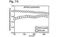
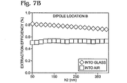
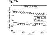
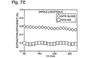
- Figs. 7A through 7E are plots of extraction efficiency as a function of organic layer 1 (h2) thickness and dipole position.
- Dipole position A is located above the center the spherical back mirror (Fig. 7A), with dipole positions B, C, D, and E, respectively associated with Figs. 7B through 7E.
- the top set of points in each graph is the light extraction efficiency into glass, and bottom set of points is the extraction efficiency into air.
- the center dipole energy (Fig. 7A) is extracted at an efficiency of ⁇ 80% into glass and ⁇ 60% into air. With the movement of dipole position to E, the extraction efficiency into glass drops to ⁇ 57% and that into air drops into ⁇ 20%. However, even the extraction efficiency at edge position E is larger than that of the planer OLED design (40% into glass and ⁇ 18% into air), see Fig. 2.
- Figs. 9A through 9F depict steps in an exemplary spherical back mirror OLED fabrication process.
- a sample is prepared with thick dielectric or semiconductor substrate, which is thicker than 1 micron.
- Fig. 9B lithography is used to define a mask.
- the substrate is wet etched to about 1.3 to 1.5 microns deep if the radius of spherical mirror is 5 microns. Due to an isotropic wet etching, a spherical 3D curve is formed.
- Fig. 9D the mask is removed and a metallic film is deposited (e.g. 100 nm thickness). The metal may be Ag, Al, Au, W, Mo, MoW, etc., with a shiny surface.
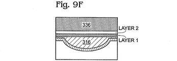
- Fig. 9E a high refractive index dielectric isolation layer is deposited by spin coating.
- organic layers 1 and 2 are deposited by spin coating or printing, and covered by a glass substrate.
- the OLED design with spherical metallic reflector increases the collimation of back propagation light.
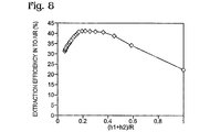
- the extraction efficiency into air is ⁇ 40% with a curvature ((h1 + h2)/R of 0.2 to 0.4), which is double that of OLED with planar metallic reflector.
- the refractive index of the isolation layer, organic layer 1 and layer 2, capsulation layer are typically close to 1.75.
- the index of glass is 1.5, and the index of air is 1.
- Fig. 10 is a flowchart illustrating a method for fabricating an OLED with a spherical back mirror. Although the method is depicted as a sequence of numbered steps for clarity, the numbering does not necessarily dictate the order of the steps. It should be understood that some of these steps may be skipped, performed in parallel, or performed without the requirement of maintaining a strict order of sequence. Generally however, the method follows the numeric order of the depicted steps. The method starts at Step 1000.
- Step 1002 provides a substrate.
- Step 1004 forms a spherical curvature in the substrate.
- Step 1006 deposits a metal film overlying the spherical curvature, forming a spherical back mirror.
- Step 1008 forms a transparent isolation layer overlying the spherical back mirror having a planar top surface.
- Step 1010 forms a transparent first electrode layer overlying the isolation layer.
- Step 1012 forms a transparent second electrode layer overlying the first electrode layer.
- Step 1014 forms a stack interposed between the first and second electrode layers comprising: an electron transport layer; a light-emitting layer adjacent to the electron transport layer; a hole transport layer adjacent to the light-emitting layer; and, a hole injection layer adjacent to the hole transport layer.
- Step 1012 is performed after Step 1014.
- Step 1016 forms an inorganic capsulation layer overlying the second electrode layer.
- Step 1018 forms a glass layer overlying the inorganic capsulation layer.
- Step 1010 forms the first electrode layer with a bottom surface
- Step 1006 forms the spherical back mirror with a spherical curve defined by a radius of curvature (R).
- Forming the stack in Step 1014 includes forming a first interface between the light-emission layer and the hole transport layer, where the distance between the first interface and the first electrode layer bottom surface is h2.
- forming the isolation layer in Step 1008 includes forming the isolation layer with a thickness (h1) between the center the spherical back mirror and the first electrode layer bottom surface, where (h1 + h2)/R is in the range of 0.2 to 0.4.
- forming the stack in Step 1014 includes h2 being in the range of 100 to 300 nm.
- the spherical back mirror formed in Step 1006 may have a value of R in the range of 3 to 110 microns and a maximum length (L) in the range of 3.6 to 176 microns, and the value of h1 formed in Step 1008 may be in the range of 0.6 to 44 microns.
- the spherical back mirror formed is Step 1006 has a uniform radius of curvature, and is made from a material such as Ag, Al, W, Mo, MoW, or Au.
- forming the insulation layer (Step 1008), first electrode layer (Step 1010), light-emitting layer, electron transport layer, hole injection layer, and hole transport layer (Step 1014), and second electrode layer (Step 1012) includes forming the above-mentioned layers having a refractive index of 1.75, with a tolerance of plus-minus 6%, in the visible wavelengths of light.
- OLED organic light emitting device
- a spherical back cavity having a metallic coating.
- An inversible light system of caustics is exploited for improving the light collimation, thereby reducing the total internal reflection in the OLED.
- a caustic is an envelope of light rays reflected or refracted by a curved surface. With the emitting layer locating at 1/5 to 2/5 of spherical radius from bottom edge of mirror, a 40% light extraction efficiency into air can be reached, which is double the 20% light extraction efficiency with planar backcavity OLED design (see Fig. 2).
- the spherical back mirror has a spherical curve (R) in a first plane orthogonal to the first electrode bottom surface and the isolation layer has a thickness (h1) between the center the spherical back mirror and the first electrode layer bottom surface.
- the thickness between the first electrode bottom surface and the light-emission layer / hole transport layer interface is h2, and typically (h1 + h2)/R is in the range of 0.2 to 0.4.
- a method for fabricating an OLED with a spherical back mirror wherein forming the spherical back mirror includes forming the spherical back mirror with a spherical curve defined by a radius of curvature (R); wherein forming the stack includes: forming the first electrode layer with a bottom surface; forming a first interface between the light-emission layer and the hole transport layer, where a distance between the first interface and the first electrode layer bottom surface is h2; wherein forming the isolation layer includes forming the isolation layer with a thickness (h1) between a center the spherical back mirror and the first electrode layer bottom surface; and, wherein (h1 + h2)/R is in a range of 0.2 to 0.4.
- R radius of curvature
- the method wherein forming the stack includes h2 being in a range of 100 to 300 nanometers (nm).
- the method wherein forming the spherical back mirror includes forming the spherical back mirror with a value of R in a range of 3 to 110 microns; and, wherein forming the isolation layer includes h1 being in a range of 0.6 to 44 microns.
- the method further comprising: forming an inorganic capsulation layer overlying the second electrode layer.
- the method further comprising: forming a glass layer overlying the inorganic capsulation layer.
- the method wherein forming the spherical back mirror includes forming the spherical back mirror with a maximum length in a range of 3.6 to 176 microns.
- the method wherein forming the spherical back mirror includes forming the spherical back mirror with a uniform radius of curvature.
- the method wherein forming the spherical back mirror includes forming the spherical back mirror from a metal selected from a group consisting of Ag, Al, W, Mo, MoW, and Au.
- the method wherein forming the insulation layer, first electrode layer, light-emitting layer, electron transport layer, hole injection layer, hole transport layer, and second electrode layer includes forming each of the above-mentioned layers having a refractive index of 1.75, with a tolerance of plus-minus 6%, in the visible wavelengths of light.
Landscapes
- Physics & Mathematics (AREA)
- Optics & Photonics (AREA)
- Electroluminescent Light Sources (AREA)
Abstract
A method is provided for fabricating an organic light emitting device (OLED) with a spherical back mirror. The method forms a spherical curvature in the substrate and deposits a metal film overlying the spherical curvature, forming a spherical back mirror. A transparent isolation layer is formed overlying the spherical back mirror having a planar top surface. A transparent first electrode layer is formed overlying the isolation layer, and a transparent second electrode layer is formed overlying the first electrode layer. A stack is interposed between the first and second electrode layers. The stack is made up of an electron transport layer adjacent the cathode, a light-emitting (electron injection) layer adjacent to the electron transport layer, a hole transport layer adjacent to the light-emitting layer, and a hole injection layer adjacent to the hole transport layer. The order of the stack layering is dependent which electrode is the anode.
Description
This invention generally relates to organic light emitting devices (OLEDs) and, more particularly, to an OLED with a spherical back mirror for improved light extraction.
As noted in Wikipedia, an OLED (organic light-emitting diode) is a light-emitting diode (LED) in which the emissive electroluminescent layer is a film of organic compound which emits light in response to an electric current. This layer of organic semiconductor is situated between two electrodes. Generally, at least one of these electrodes is transparent. OLEDs are used to create digital displays in devices such as television screens, computer monitors, portable systems such as mobile phones, handheld games consoles, and PDAs.
There are two main families of OLEDs: those based on small molecules and those employing polymers. Adding mobile ions to an OLED creates a light-emitting electrochemical cell, which has a slightly different mode of operation. OLED displays can use either passive-matrix (PMOLED) or active-matrix addressing schemes. Active-matrix OLEDs (AMOLED) require a thin-film transistor backplane to switch each individual pixel on or off, but allow for higher resolution and larger display sizes.
An OLED display works without a backlight. Thus, it can display deep black levels and can be thinner and lighter than a liquid crystal display (LCD). In low ambient light conditions such as a dark room an OLED screen can achieve a higher contrast ratio than an LCD, whether the LCD uses cold cathode fluorescent lamps or LED backlight.
Multilayer OLEDs can be fabricated with two or more layers in order to improve device efficiency. As well as conductive properties, different materials may be chosen to aid charge injection at the electrodes by providing a more gradual electronic profile, or block a charge from reaching the opposite electrode and being wasted. Many modern OLEDs incorporate a simple bilayer structure, consisting of a conductive layer and an emissive layer. The emissive layer may be understood as comprising a light-emission or electron injection layer, and an electron transport layer. Likewise, the conductive layer may be understood as comprising a hole injection layer and a hole transport layer.
During operation, a voltage is applied across the OLED such that the anode is positive with respect to the cathode. A current of electrons flows through the device from cathode to anode, as electrons are injected into the lowest unoccupied molecular orbit (LUMO) of the organic layer at the cathode and withdrawn from the highest occupied molecular orbit (HOMO) at the anode. This latter process may also be described as the injection of electron holes into the HOMO. Electrostatic forces bring the electrons and the holes towards each other and they recombine forming an exciton, a bound state of the electron and hole. This happens closer to the emissive layer, because in organic semiconductors holes are generally more mobile than electrons. The decay of this excited state results in a relaxation of the energy levels of the electron, accompanied by emission of radiation whose frequency is in the visible region. The frequency of this radiation depends on the band gap of the material, in this case the difference in energy between the HOMO and LUMO.
Indium tin oxide (ITO) is commonly used as the anode material. It is transparent to visible light and has a high work function which promotes injection of holes into the HOMO level of the organic layer. A typical conductive layer may consist of poly(3,4-ethylenedioxythiophene):poly(styrenesulfonate) [PEDOT:PSS] as the HOMO level of this material generally lies between the workfunction of ITO and the HOMO of other commonly used polymers, reducing the energy barriers for hole injection. Metals such as barium and calcium are often used for the cathode as they have low work functions which promote injection of electrons into the LUMO of the organic layer. Such metals are reactive, so they require a capping layer of aluminum to avoid degradation.
Fig. 1 is a partial cross-sectional view of an OLED (prior art). Layer 1 represents a stack comprising an electron transport layer, electron injection layer, and a cathode electrode. Likewise, layer 2 represents a stack comprising a hole transport layer, hole injection layer, and the anode electrode. Electron emission occurs at the interface between layer 1 and layer 2. The figure depicts energy loss in OLED structure due to the internal total reflection of high index waveguide.










For example, if
 ,
,
 , and
, and
 , the critical angle of
 ,
,
 , and
, and
 . A back reflecting mirror can collected particle light and enhanced extraction efficiency. However, only the back propagation of light at
 can be extracted out. The back propagation of light at
 is confined in isolation layer (n=n1). The back propagation light with
 is confined in the media of index
 and
and
 .
.
Fig. 2 is a plot of the external extraction efficiency of the structure of Fig. 1 plotted as a function of organic layer 1 (OL1) thickness using a finite-difference time-domain simulation (prior art). The light source is located at the interface of organic layer 1 and organic layer 2. The light source is an incoherent dipole source at a wavelength of 450 nanometers (nm). The extraction efficiency into substrate is ~43% and that into air is close to 20% at 450 nm, with the thickness of layer 2 set to 250 nm.
It would be advantageous if the light extraction efficiency of an OLED could be improved.
Disclosed herein is an organic light emitting device (OLED) device with a spherical back cavity.
Accordingly, a method is provided for fabricating an organic light emitting device (OLED) with a spherical back mirror. The method forms a spherical curvature in the substrate and deposits a metal film overlying the spherical curvature, forming a spherical back mirror. A transparent isolation layer is formed overlying the spherical back mirror having a planar top surface. A transparent first electrode layer is formed overlying the isolation layer, and a transparent second electrode layer is formed overlying the first electrode layer. A stack is interposed between the first and second electrode layers. The stack is made up of an electron transport layer adjacent the cathode, a light-emitting (electron injection) layer adjacent to the electron transport layer, a hole transport layer adjacent to the light-emitting layer, and a hole injection layer adjacent to the hole transport layer. The order of the stack layering is dependent upon which electrode is the anode and which electrode is the cathode.
Figs. 3A and 3B are partial cross-sectional views of an OLED with a spherical back mirror. The OLED 300 comprises a transparent first electrode layer 302 and a transparent second electrode layer 304 overlying the first electrode layer. An electron transport layer 306 is interposed between the first electrode layer 302 and second electrode layer 304. A light-emitting or electron injection layer 308 is adjacent to (i.e. in direct contact with) the electron transport layer 306. A hole transport layer 310 is adjacent to the light-emitting layer 308. A hole injection layer 312 is adjacent to the hole transport layer 310. A spherical back mirror concave top surface 314 underlies the first electrode layer 302. A transparent isolation layer 316 is interposed between the first electrode layer 302 and the spherical back mirror concave surface 314. As shown in Fig. 3A, the first electrode 302 is a cathode. As shown in Fig. 3B, the first electrode 302 is an anode.
Referencing either Fig. 3A or 3B, the first electrode layer 302 has a bottom surface 318. The spherical back mirror 320 has a spherical curve defined by the radius of curvature (R) 322. The isolation layer 316 has a thickness (h1) 326 between the center the spherical back mirror 320 and the first electrode layer bottom surface 318. A first interface 330 exists between the light-emission layer 308 and the hole transport layer 310, and the distance between the first interface and the first electrode layer bottom surface is h2 (332). In one aspect, (h1 + h2)/R is in the range of 0.2 to 0.4. In the case of a circular-shaped spherical back mirror 320, the spherical curve is defined by a uniform radius of curvature (the spherical shape is circular as seen from above). Otherwise, the spherical back mirror 320 may have a non-circular shape. Typically, the spherical back mirror 320 has a maximum length 328 in the range of 3.6 to 176 microns. The maximum length of the spherical back mirror is driven by the value of R, which is selected for the desired size of the pixel.
In one aspect h2 is in the range of 100 to 300 nanometers (nm). It is also typical that the value of R be in the range of 3 to 110 microns, and h1 be in the range of 0.6 to 44 microns. However, it should be understood that the OLED 300 is not limited to any particular physical dimensions.
Regarding the h2 ranges, the OLEDs are sized for use in displays. To be functional in displays, h2 must not be too thin or too thick. The h2 size range stated above is an example of a suitable range. The value for R is selected to yield OLED pixels of the desired size. The value range for h1 is driven by the values selected for R and h2. None of the numerical ranges stated above is absolute; they are suggested ranges for embodiments within the scope of the invention.
In one aspect as shown in Fig. 3A, the OLED 300 further comprises an inorganic capsulation layer 334 overlying the second electrode layer 304. In another aspect as shown in Fig. 3B, the OLED further comprises both the inorganic capsulation layer 334 and a glass (or like material) layer 336 overlying the inorganic capsulation layer 334. Note: although not shown, the device of Fig. 3B made be made without the glass layer and the device of Fig. 3A may include a glass layer.
In one aspect, the spherical back mirror 320 is a material such as Ag, Al, W, Mo, MoW, or Au. However, other highly reflective materials (e.g. with a reflectivity of greater than 90% in the visible wavelengths of light) may be used. In another aspect, the insulation layer, first electrode layer, light-emitting layer, electron transport layer, hole injection layer, hole transport layer, and second electrode layer have a refractive index of 1.75, with a tolerance of plus-minus 6%, in the visible wavelengths of light.
The materials of the h2 layer have a relatively high index of refraction, which is why it is desirable to have relatively high refractive indices in the other adjacent layers, to match that of h2.
Fig. 4 is a diagram depicting the reflective caustics of parallel lines upon a circular reflective surface. The OLEDs described above take advantage of the caustics associated with a spherical metallic surface. Area 400 includes a condensed ray density associated with large reflected angles. h1 is the distance from area 400 to the bottom of curve, and R is the radius of the curve. Because optical ray tracing is an inversible system, this system can be used for OLED design. When the emitting layer of OLED is located within area 400, a substantial portion of the back propagation light is reflected out of the device in collimation, thereby reducing total internal reflection. Roughly, the range of distance values for points inside area 400 is around 0.2R to 0.4R for the best OLED extraction efficiency. In one aspect, the distance to the bottom of area 400 (h1) divided by R is 0.2, and the distance to the top of area 400 divided by R is 0.4.
Fig. 5 is a partial cross-sectional of the device of Fig. 3A or 3B. Here, the cathode, electron transport, and light-emitting layer are represented by either layer 1 or layer 2. Likewise, the anode, hole injection, and hole transport layer are represented by the other of layer 1 or layer 2. For example, if the cathode, electron transport, and light-emitting layer are layer 1, then the anode, hole injection, and hole transport layer are layer 2. As shown in the figure, some back propagation rays are extracted out of the device without being lost to total internal reflection. In one example, the length (L) and width (not shown) are both 12 microns. The radius of the spherical curve (R) is 5 microns, and h1 is 1.4 microns.
Fig. 6 is a schematic diagram depicting a light source at five three-dimensional dipole positions along the plane of the first interface.
Figs. 7A through 7E are plots of extraction efficiency as a function of organic layer 1 (h2) thickness and dipole position. Dipole position A is located above the center the spherical back mirror (Fig. 7A), with dipole positions B, C, D, and E, respectively associated with Figs. 7B through 7E. The top set of points in each graph is the light extraction efficiency into glass, and bottom set of points is the extraction efficiency into air.
The center dipole energy (Fig. 7A) is extracted at an efficiency of ~80% into glass and ~ 60% into air. With the movement of dipole position to E, the extraction efficiency into glass drops to ~57% and that into air drops into ~ 20%. However, even the extraction efficiency at edge position E is larger than that of the planer OLED design (40% into glass and ~18% into air), see Fig. 2.
Fig. 8 is a graph depicting the light extraction efficiency from a planar light source, into air, as a function of (h1 + h2)/R. With (h1 + h2)/R values from 0.2 to 0.4, the extraction efficiency is above 40%, which means for a R = 5 micron spherical mirror, the h1 can be ranged from 1 to 2 microns, which gives the design a large tolerance for easy fabrication.
Figs. 9A through 9F depict steps in an exemplary spherical back mirror OLED fabrication process. In Fig. 9A a sample is prepared with thick dielectric or semiconductor substrate, which is thicker than 1 micron. In Fig. 9B lithography is used to define a mask. In Fig. 9C the substrate is wet etched to about 1.3 to 1.5 microns deep if the radius of spherical mirror is 5 microns. Due to an isotropic wet etching, a spherical 3D curve is formed. In Fig. 9D the mask is removed and a metallic film is deposited (e.g. 100 nm thickness). The metal may be Ag, Al, Au, W, Mo, MoW, etc., with a shiny surface. In Fig. 9E a high refractive index dielectric isolation layer is deposited by spin coating. In Fig. 9F organic layers 1 and 2 are deposited by spin coating or printing, and covered by a glass substrate.
In summary, the OLED design with spherical metallic reflector increases the collimation of back propagation light. The extraction efficiency into air is ~40% with a curvature ((h1 + h2)/R of 0.2 to 0.4), which is double that of OLED with planar metallic reflector. The refractive index of the isolation layer, organic layer 1 and layer 2, capsulation layer are typically close to 1.75. The index of glass is 1.5, and the index of air is 1.
Fig. 10 is a flowchart illustrating a method for fabricating an OLED with a spherical back mirror. Although the method is depicted as a sequence of numbered steps for clarity, the numbering does not necessarily dictate the order of the steps. It should be understood that some of these steps may be skipped, performed in parallel, or performed without the requirement of maintaining a strict order of sequence. Generally however, the method follows the numeric order of the depicted steps. The method starts at Step 1000.
More particularly, Step 1010 forms the first electrode layer with a bottom surface, and Step 1006 forms the spherical back mirror with a spherical curve defined by a radius of curvature (R). Forming the stack in Step 1014 includes forming a first interface between the light-emission layer and the hole transport layer, where the distance between the first interface and the first electrode layer bottom surface is h2. Then, forming the isolation layer in Step 1008 includes forming the isolation layer with a thickness (h1) between the center the spherical back mirror and the first electrode layer bottom surface, where (h1 + h2)/R is in the range of 0.2 to 0.4. In another aspect, forming the stack in Step 1014 includes h2 being in the range of 100 to 300 nm. Continuing the example, the spherical back mirror formed in Step 1006 may have a value of R in the range of 3 to 110 microns and a maximum length (L) in the range of 3.6 to 176 microns, and the value of h1 formed in Step 1008 may be in the range of 0.6 to 44 microns. Typically, the spherical back mirror formed is Step 1006 has a uniform radius of curvature, and is made from a material such as Ag, Al, W, Mo, MoW, or Au.
In one aspect, forming the insulation layer (Step 1008), first electrode layer (Step 1010), light-emitting layer, electron transport layer, hole injection layer, and hole transport layer (Step 1014), and second electrode layer (Step 1012) includes forming the above-mentioned layers having a refractive index of 1.75, with a tolerance of plus-minus 6%, in the visible wavelengths of light.
An OLED with spherical back mirror has been presented. Examples of particular dimensions, materials, and processes have been presented to illustrate the invention. However, the invention is not limited to merely these examples. Although the OLED has been described in the context of a bilayer device, the OLED is not limited to any particular number of layers. Other variations and embodiments of the invention will occur to those skilled in the art.
(OTHER DESCRIPTIONS 1)
(OTHER DESCRIPTIONS 1)
Disclosed herein is an organic light emitting device (OLED) device with a spherical back cavity having a metallic coating. An inversible light system of caustics is exploited for improving the light collimation, thereby reducing the total internal reflection in the OLED. A caustic is an envelope of light rays reflected or refracted by a curved surface. With the emitting layer locating at 1/5 to 2/5 of spherical radius from bottom edge of mirror, a 40% light extraction efficiency into air can be reached, which is double the 20% light extraction efficiency with planar backcavity OLED design (see Fig. 2).
A fabrication process flow is also provided. After lithography, a spherical bowl shape is fabricated by isotropic wet etching, following the metallic deposition of Ag, Al, Au, W, Mo, or MoW, and then spin coating a high index of refraction (e.g. n=1.75) isolation layer, organic layers, and cathode/anode layers. A glass substrate may cap the top of the device.
The spherical back mirror has a spherical curve (R) in a first plane orthogonal to the first electrode bottom surface and the isolation layer has a thickness (h1) between the center the spherical back mirror and the first electrode layer bottom surface. The thickness between the first electrode bottom surface and the light-emission layer / hole transport layer interface is h2, and typically (h1 + h2)/R is in the range of 0.2 to 0.4.
Additional details of the above described method and an OLED with a spherical back mirror are provided above.
(OTHER DESCRIPTIONS 2)
(OTHER DESCRIPTIONS 2)
In some embodiments, a method for fabricating an OLED with a spherical back mirror wherein forming the spherical back mirror includes forming the spherical back mirror with a spherical curve defined by a radius of curvature (R);
wherein forming the stack includes:
forming the first electrode layer with a bottom surface;
forming a first interface between the light-emission layer and the hole transport layer, where a distance between the first interface and the first electrode layer bottom surface is h2;
wherein forming the isolation layer includes forming the isolation layer with a thickness (h1) between a center the spherical back mirror and the first electrode layer bottom surface; and,
wherein (h1 + h2)/R is in a range of 0.2 to 0.4.
wherein forming the stack includes:
forming the first electrode layer with a bottom surface;
forming a first interface between the light-emission layer and the hole transport layer, where a distance between the first interface and the first electrode layer bottom surface is h2;
wherein forming the isolation layer includes forming the isolation layer with a thickness (h1) between a center the spherical back mirror and the first electrode layer bottom surface; and,
wherein (h1 + h2)/R is in a range of 0.2 to 0.4.
In some embodiments, the method wherein forming the stack includes h2 being in a range of 100 to 300 nanometers (nm).
In some embodiments, the method wherein forming the spherical back mirror includes forming the spherical back mirror with a value of R in a range of 3 to 110 microns; and,
wherein forming the isolation layer includes h1 being in a range of 0.6 to 44 microns.
wherein forming the isolation layer includes h1 being in a range of 0.6 to 44 microns.
In some embodiments, the method further comprising:
forming an inorganic capsulation layer overlying the second electrode layer.
forming an inorganic capsulation layer overlying the second electrode layer.
In some embodiments, the method further comprising:
forming a glass layer overlying the inorganic capsulation layer.
forming a glass layer overlying the inorganic capsulation layer.
In some embodiments, the method wherein forming the spherical back mirror includes forming the spherical back mirror with a maximum length in a range of 3.6 to 176 microns.
In some embodiments, the method wherein forming the spherical back mirror includes forming the spherical back mirror with a uniform radius of curvature.
In some embodiments, the method wherein forming the spherical back mirror includes forming the spherical back mirror from a metal selected from a group consisting of Ag, Al, W, Mo, MoW, and Au.
In some embodiments, the method wherein forming the insulation layer, first electrode layer, light-emitting layer, electron transport layer, hole injection layer, hole transport layer, and second electrode layer includes forming each of the above-mentioned layers having a refractive index of 1.75, with a tolerance of plus-minus 6%, in the visible wavelengths of light.
(OTHER DESCRIPTIONS 3)
(OTHER DESCRIPTIONS 3)
For a fuller understanding of the nature and advantages of the invention, reference should be made to the ensuing detailed description taken in conjunction with the accompanying drawings.
The invention being thus described, it will be obvious that the same way may be varied in many ways. Such variations are not to be regarded as a departure from the spirit and scope of the invention, and all such modifications as would be obvious to one skilled in the art are intended to be included within the scope of the following claims.
Claims (11)
- An organic light emitting device (OLED) with a spherical back mirror, the OLED comprising:
a transparent first electrode layer;
a transparent second electrode layer overlying the first electrode layer;
an electron transport layer interposed between the first and second electrode layers;
a light-emitting layer adjacent to the electron transport layer;
a hole transport layer adjacent to the light-emitting layer;
a hole injection layer adjacent to the hole transport layer; and,
a spherical back mirror concave top surface underlying the first electrode layer. - The OLED of claim 1 further comprising:
a transparent isolation layer interposed between the first electrode layer and the spherical back mirror concave surface. - The OLED of claim 2 wherein the first electrode layer has a bottom surface;
wherein the spherical back mirror has a spherical curve defined by a radius of curvature (R);
wherein a first interface exists between the light-emission layer and the hole transport layer;
wherein a distance between the first interface and the first electrode layer bottom surface is h2;
wherein the isolation layer has a thickness (h1) between a center the spherical back mirror and the first electrode layer bottom surface; and,
wherein (h1 + h2)/R is in a range of 0.2 to 0.4. - The OLED of claim 3 wherein h2 is in a range of 100 to 300 nanometers (nm);
wherein the spherical back mirror has a value of R in a range of 3 to 110 microns; and,
wherein h1 is in a range of 0.6 to 44 microns. - The OLED of claim 1 further comprising:
an inorganic capsulation layer overlying the second electrode layer. - The OLED of claim 5 further comprising:
a glass layer overlying the inorganic capsulation layer. - The OLED of claim 3 wherein the spherical back mirror has a maximum length in a range of 3.6 to 176 microns.
- The OLED of claim 1 wherein the spherical back mirror has a uniform radius of curvature.
- The OLED of claim 1 wherein the spherical back mirror is a material selected from a group consisting of Ag, Al, W, Mo, MoW, and Au.
- The OLED of claim 1 wherein the insulation layer, first electrode layer, light-emitting layer, electron transport layer, hole injection layer, hole transport layer, and second electrode layer each have a refractive index of 1.75, with a tolerance of plus-minus 6%, in the visible wavelengths of light.
- A method for fabricating an organic light emitting device (OLED) with a spherical back mirror, the method comprising:
providing a substrate;
forming a spherical curvature in the substrate;
depositing a metal film overlying the spherical curvature, forming a spherical back mirror;
forming a transparent isolation layer overlying the spherical back mirror having a planar top surface;
forming a transparent first electrode layer overlying the isolation layer;
forming a transparent second electrode layer overlying the first electrode layer;
forming a stack interposed between the first and second electrode layers comprising:
an electron transport layer;
a light-emitting layer adjacent to the electron transport layer;
a hole transport layer adjacent to the light-emitting layer; and,
a hole injection layer adjacent to the hole transport layer.
Applications Claiming Priority (2)
| Application Number | Priority Date | Filing Date | Title |
|---|---|---|---|
| US13/797,340 | 2013-03-12 | ||
| US13/797,340 US8921839B2 (en) | 2013-03-12 | 2013-03-12 | Light emitting device with spherical back mirror |
Publications (1)
| Publication Number | Publication Date |
|---|---|
| WO2014141702A1 true WO2014141702A1 (en) | 2014-09-18 |
Family
ID=51523569
Family Applications (1)
| Application Number | Title | Priority Date | Filing Date |
|---|---|---|---|
| PCT/JP2014/001405 Ceased WO2014141702A1 (en) | 2013-03-12 | 2014-03-12 | Organic light emitting device (oled) and method for fabricating oled |
Country Status (2)
| Country | Link |
|---|---|
| US (1) | US8921839B2 (en) |
| WO (1) | WO2014141702A1 (en) |
Cited By (1)
| Publication number | Priority date | Publication date | Assignee | Title |
|---|---|---|---|---|
| WO2016084759A1 (en) * | 2014-11-28 | 2016-06-02 | シャープ株式会社 | Organic electroluminescence device, illumination device, and display device |
Families Citing this family (12)
| Publication number | Priority date | Publication date | Assignee | Title |
|---|---|---|---|---|
| US9496522B2 (en) * | 2013-12-13 | 2016-11-15 | Universal Display Corporation | OLED optically coupled to curved substrate |
| WO2016043113A1 (en) * | 2014-09-16 | 2016-03-24 | シャープ株式会社 | Organic electroluminescence device and method for manufacturing organic electroluminescence device |
| US10224512B2 (en) * | 2014-09-18 | 2019-03-05 | Sharp Kabushiki Kaisha | Organic electroluminescent device and method for producing organic electroluminescent device |
| US10199605B2 (en) * | 2014-11-20 | 2019-02-05 | Sharp Kabushiki Kaisha | Organic electroluminescence device and method for manufacturing organic electroluminescence device |
| US10826021B2 (en) * | 2015-09-10 | 2020-11-03 | Sharp Kabushiki Kaisha | Organic electroluminescence device including a plurality of unit regions each including a light emitting area and a transmissive area |
| US10418592B2 (en) | 2015-11-16 | 2019-09-17 | Sharp Kabushiki Kaisha | Organic electroluminescence device, production method for organic electroluminescence device, illumination device and display device |
| CN106355160A (en) * | 2016-09-06 | 2017-01-25 | 京东方科技集团股份有限公司 | Pattern recognition device and electronic equipment |
| CN110148685B (en) * | 2019-05-07 | 2021-01-15 | 深圳市华星光电半导体显示技术有限公司 | Display panel and method of making the same |
| CN110085655B (en) * | 2019-05-30 | 2021-01-26 | 京东方科技集团股份有限公司 | Display panel, method for manufacturing the same, and display device |
| WO2021088037A1 (en) | 2019-11-08 | 2021-05-14 | 京东方科技集团股份有限公司 | Array substrate and manufacturing method thereof, display panel, and display device |
| US12598962B2 (en) | 2023-03-14 | 2026-04-07 | Adeia Semiconductor Bonding Technologies Inc. | System and method for bonding transparent conductor substrates |
| US20250364512A1 (en) * | 2024-05-22 | 2025-11-27 | Adeia Semiconductor Bonding Technologies Inc. | Stacking of optical structures using conductive materials and reflectors |
Citations (3)
| Publication number | Priority date | Publication date | Assignee | Title |
|---|---|---|---|---|
| WO2003096755A1 (en) * | 2002-05-14 | 2003-11-20 | Casio Computer Co., Ltd. | Luminescent panel |
| JP2006221902A (en) * | 2005-02-09 | 2006-08-24 | Seiko Epson Corp | LIGHT EMITTING DEVICE, MANUFACTURING METHOD THEREOF, IMAGE PRINTING DEVICE, AND IMAGE READING DEVICE |
| JP2007207529A (en) * | 2006-01-31 | 2007-08-16 | Kyocera Corp | Organic EL display |
Family Cites Families (7)
| Publication number | Priority date | Publication date | Assignee | Title |
|---|---|---|---|---|
| WO2009009695A1 (en) | 2007-07-10 | 2009-01-15 | University Of Florida Research Foundation, Inc. | Top-emission organic light-emitting devices with microlens arrays |
| DE112009001122A5 (en) | 2008-05-07 | 2011-03-24 | Peter Dr.-Ing. Draheim | Apparatus and method for concentrating incident light |
| DE102008053326A1 (en) * | 2008-07-25 | 2010-01-28 | Osram Opto Semiconductors Gmbh | A radiation-emitting device and method for producing a radiation-emitting device |
| US7957621B2 (en) | 2008-12-17 | 2011-06-07 | 3M Innovative Properties Company | Light extraction film with nanoparticle coatings |
| US10581020B2 (en) | 2011-02-08 | 2020-03-03 | Vitro Flat Glass Llc | Light extracting substrate for organic light emitting diode |
| US8538224B2 (en) | 2010-04-22 | 2013-09-17 | 3M Innovative Properties Company | OLED light extraction films having internal nanostructures and external microstructures |
| US9293734B2 (en) | 2010-12-23 | 2016-03-22 | Universal Display Corporation | Light extraction block with curved surface |
-
2013
- 2013-03-12 US US13/797,340 patent/US8921839B2/en not_active Expired - Fee Related
-
2014
- 2014-03-12 WO PCT/JP2014/001405 patent/WO2014141702A1/en not_active Ceased
Patent Citations (3)
| Publication number | Priority date | Publication date | Assignee | Title |
|---|---|---|---|---|
| WO2003096755A1 (en) * | 2002-05-14 | 2003-11-20 | Casio Computer Co., Ltd. | Luminescent panel |
| JP2006221902A (en) * | 2005-02-09 | 2006-08-24 | Seiko Epson Corp | LIGHT EMITTING DEVICE, MANUFACTURING METHOD THEREOF, IMAGE PRINTING DEVICE, AND IMAGE READING DEVICE |
| JP2007207529A (en) * | 2006-01-31 | 2007-08-16 | Kyocera Corp | Organic EL display |
Cited By (2)
| Publication number | Priority date | Publication date | Assignee | Title |
|---|---|---|---|---|
| WO2016084759A1 (en) * | 2014-11-28 | 2016-06-02 | シャープ株式会社 | Organic electroluminescence device, illumination device, and display device |
| US10157967B2 (en) | 2014-11-28 | 2018-12-18 | Sharp Kabushiki Kaisha | Organic electroluminescence device, illumination device, and display device |
Also Published As
| Publication number | Publication date |
|---|---|
| US20140264291A1 (en) | 2014-09-18 |
| US8921839B2 (en) | 2014-12-30 |
Similar Documents
| Publication | Publication Date | Title |
|---|---|---|
| US8921839B2 (en) | Light emitting device with spherical back mirror | |
| US7772762B2 (en) | White light organic electroluminescent element | |
| US7825570B2 (en) | LED device having improved contrast | |
| EP2503620A1 (en) | Organic electroluminescent device, display device, and illumination device | |
| EP3018721B1 (en) | Substrate for organic light emitting device and organic light emitting device comprising same | |
| TW200527951A (en) | Luminous device, its manufacture and electronic apparatus | |
| US9431633B2 (en) | Organic light emitting diode display device | |
| CN105789260B (en) | Transparent display panel and preparation method thereof | |
| US20170352840A1 (en) | Method for manufacturing light extraction substrate for organic light-emitting element, light extraction substrate for organic light-emitting element, and organic light-emitting element comprising same | |
| JP7201442B2 (en) | Display panel and its manufacturing method, electroluminescence device and display device | |
| CN106601773A (en) | Double-sided OLED display device and the manufacturing method for the same | |
| CN101751832B (en) | Organic light emitting diode display | |
| KR101650541B1 (en) | Flexible substrate and method of fabricating thereof | |
| CN100565967C (en) | Organic light-emitting device and manufacturing method thereof | |
| KR20160001876A (en) | Organic light emitting diode display device | |
| EP2720284B1 (en) | Method of fabricating a metal oxide thin film substrate for OLED | |
| US20170358763A1 (en) | Flexible substrate and method of manufacturing same | |
| TWI673898B (en) | Light extraction substrate for organic light-emitting diode, method of fabricating the same, and organic light-emitting diode device including the same | |
| US20130149803A1 (en) | Method of fabricating organic light emitting diode | |
| CN1717139A (en) | Organic electro-luminescence display device and fabricating method thereof | |
| KR101489780B1 (en) | Organic light emitting diode and fabrication method the same | |
| JP2008500695A (en) | Composite optical breakdown electrode for high-contrast electroluminescent devices | |
| KR101699275B1 (en) | Light extraction substrate for oled, method of fabricating thereof and oled including the same | |
| US20170352839A1 (en) | Light extracting substrate for organic light emitting device, method of manufacturing same, and organic light emitting device including same | |
| KR101436548B1 (en) | Light extraction substrate, and method of fabricating light extraction substrate for oled |
Legal Events
| Date | Code | Title | Description |
|---|---|---|---|
| 121 | Ep: the epo has been informed by wipo that ep was designated in this application |
Ref document number: 14763749 Country of ref document: EP Kind code of ref document: A1 |
|
| NENP | Non-entry into the national phase |
Ref country code: DE |
|
| 122 | Ep: pct application non-entry in european phase |
Ref document number: 14763749 Country of ref document: EP Kind code of ref document: A1 |