WO2014136288A1 - 超電導磁気シールド装置及びその製造方法 - Google Patents
超電導磁気シールド装置及びその製造方法 Download PDFInfo
- Publication number
- WO2014136288A1 WO2014136288A1 PCT/JP2013/071403 JP2013071403W WO2014136288A1 WO 2014136288 A1 WO2014136288 A1 WO 2014136288A1 JP 2013071403 W JP2013071403 W JP 2013071403W WO 2014136288 A1 WO2014136288 A1 WO 2014136288A1
- Authority
- WO
- WIPO (PCT)
- Prior art keywords
- magnetic shield
- superconducting
- axial
- tape
- superconducting material
- Prior art date
- Legal status (The legal status is an assumption and is not a legal conclusion. Google has not performed a legal analysis and makes no representation as to the accuracy of the status listed.)
- Ceased
Links
Images









Classifications
-
- H—ELECTRICITY
- H05—ELECTRIC TECHNIQUES NOT OTHERWISE PROVIDED FOR
- H05K—PRINTED CIRCUITS; CASINGS OR CONSTRUCTIONAL DETAILS OF ELECTRIC APPARATUS; MANUFACTURE OF ASSEMBLAGES OF ELECTRICAL COMPONENTS
- H05K9/00—Screening of apparatus or components against electric or magnetic fields
- H05K9/0073—Shielding materials
- H05K9/0075—Magnetic shielding materials
- H05K9/0077—Magnetic shielding materials comprising superconductors
Definitions
- the present invention relates to a superconducting magnetic shield device that performs magnetic shielding using a high-temperature superconductor and a method for manufacturing the same.
- a weak magnetic field measuring device that measures a weak magnetic field such as a magnetoencephalograph or a magnetocardiograph measures this as a disturbance when an external magnetic field such as geomagnetism is applied. For this reason, the weak magnetic field measurement device is shielded by a magnetic shield device that shields the external magnetic field that becomes a disturbance so that the disturbance does not adversely affect the weak magnetic field measurement device, thereby measuring the weak magnetic field.
- this magnetic shield device there is one in which the entire inner wall of a room in which a weak magnetic field measuring device is installed is made of a magnetic shield material, and this magnetic shield room prevents the influence of an external magnetic field (see Patent Document 1). .
- the magnetic shield room is configured to magnetically shield the entire room, it becomes a large-scale facility.
- This superconducting magnetic shield device has a configuration in which a superconductor having a Meissner effect is disposed on a cylindrical base material, and shields the magnetic field in the target space by the complete diamagnetism of the superconductor when geomagnetism or the like is applied. This makes it possible to measure a weak magnetic field without being affected by an external magnetic field such as geomagnetism.
- JP 2002-291713 A Japanese Patent Laid-Open No. 10-313135
- the superconducting material constituting the superconducting magnetic shield there are a low-temperature superconducting material and a high-temperature superconducting material.
- a low-temperature superconducting material is used as the material of the superconducting magnetic shield
- the superconducting magnetic shield having a large-diameter cylindrical shape can be manufactured relatively easily because the low-temperature superconducting material is easy to mold.
- the cooling temperature is 80 K or less and cooling is easy, but the production of the high-temperature superconducting material is troublesome.
- a high temperature superconducting material is formed on a cylindrical substrate by thermal spraying.
- this work is troublesome and requires a long time for production, and there is a problem that the product cost becomes high.
- the superconducting magnetic shield device requires a size corresponding to this because a person enters the superconducting magnetic shield formed in a cylindrical shape.
- the conventional superconducting magnetic shield using the high-temperature superconducting material cannot be partially repaired because it is an integral body.
- the conventional superconducting magnetic shield device has a problem that the yield is low and the risk relating to manufacturing is high.
- a more detailed object of the present invention is to provide a superconducting magnetic shield device that can facilitate assembly, improve yield, and reduce costs even when a high-temperature superconducting material is used, and a method for manufacturing the same.
- the present invention provides: A transverse magnetic shield made of a superconducting material for transverse direction, which is arranged perpendicularly or inclined with respect to the axial direction of the axial magnetic shield and connected to the axial magnetic shield; A support for supporting the axial magnetic shield and the transverse magnetic shield.
- the superconducting magnetic shield device is configured by the axial magnetic shield and the lateral magnetic shield, the assembly of the superconducting magnetic shield device is facilitated, the yield is improved, and the cost is reduced. In addition, even when an axial magnetic field and a transverse magnetic field are applied, this can be reliably shielded.
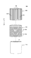
- 1 is a perspective view of a superconducting magnetic shield device according to a first embodiment of the present invention.
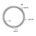
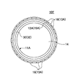
- 1 is a plan view of a superconducting magnetic shield device according to a first embodiment of the present invention.
- 1 is an exploded perspective view of a superconducting magnetic shield device according to a first embodiment of the present invention. It is a perspective view which expands and shows the tape-shaped superconducting material for axial directions. It is sectional drawing which expands and shows the joining position of the tape-shaped superconducting material for axial directions, and the tape-shaped superconducting material for horizontal directions. It is a figure which shows the eddy current which generate
- FIG. 1 to 3 show a superconducting magnetic shield device 10A according to the first embodiment of the present invention.
- 1 is a perspective view of a superconducting magnetic shield device 10A
- FIG. 2 is a plan view
- FIG. 3 is an exploded perspective view.
- the superconducting magnetic shield device 10A is applied to a weak magnetic field measurement device that measures a weak magnetic field such as a magnetoencephalograph or a magnetocardiograph.
- the superconducting magnetic shield device 10A has a support 11A, an axial magnetic shield 12A, a lateral magnetic shield 13A, and the like.
- the support 11A is disposed on the innermost periphery
- the axial magnetic shield 12A is disposed on the outer periphery thereof
- the lateral magnetic shield 13A is disposed on the outer periphery thereof. Therefore, the superconducting magnetic shield device 10A has a structure in which the support 11A, the axial magnetic shield 12A, and the lateral magnetic shield 13A are overlapped in triplicate.
- the superconducting magnetic shield device 10A has a cylindrical shape as a whole. Therefore, the space part 14 is formed in the central part, and when the superconducting magnetic shield device 10A is applied to a magnetoencephalograph, the magnetoencephalometer is disposed inside the space part 14 and The person's head is inserted.
- each component constituting the superconducting magnetic shield device 10A will be described.
- the support 11A has a cylindrical shape and supports the axial magnetic shield 12A and the lateral magnetic shield 13A.
- the material of the support 11A is not particularly limited, but in the present embodiment, a resin or metal that is nonmagnetic and has good moldability is used. Specifically, FRP (glass fiber reinforced plastic) or the like can be used. Further, a cooling pipe through which a refrigerant for cooling the magnetic shields 12 and 13A flows may be disposed on the inner periphery of the support 11A.
- the axial magnetic shield 12A shields against an axial magnetic field.
- the magnetic field in the axial direction of the cylinder (directions indicated by arrows Z1 and Z2 in the figure) is called the axial magnetic field
- the magnetic field in the direction orthogonal to the axial direction of the cylinder is called the transverse magnetic field.
- a magnetic shield against an axial magnetic field is called an axial magnetic shield
- a magnetic shield against a transverse magnetic field is called a transverse magnetic shield.
- a magnetic field applied from a direction other than the axial direction or the lateral direction can be decomposed into an axial component (axial magnetic field component) and a lateral component (lateral magnetic field component). For this reason, in the following description, only an axial magnetic field and a transverse magnetic field will be described.
- the axial magnetic shield 12A has a configuration in which a plurality of axial tape-like superconducting materials 15A are stacked (stacked) in the axial direction of the support 11A.
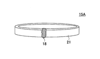
- the axial tape-shaped superconducting material 15 ⁇ / b> A may be formed by bending the tape-shaped superconducting material 21 into a ring shape and joining both ends thereof with solder 18.
- the tape-shaped superconducting material 21 a superconducting material whose outer periphery is covered with a metal or a high-temperature superconducting material formed on a metal substrate can be used. Further, as the superconducting material, a high temperature superconducting material having a high critical temperature is used. As this tape-shaped superconducting material 21, for example, DI-BSCCO (product name) manufactured by Sumitomo Electric Industries, Ltd. can be used.
- the tape-shaped superconducting material 21 configured in this way has higher mechanical strength and resistance to distortion than the case of a single superconducting material. For this reason, even if the tape-shaped superconducting material 21 is formed in a loop shape as shown in FIG. 4, the high-temperature superconducting material is not damaged by the distortion, and the yield can be improved. Further, since the tape-shaped superconducting material 21 and the axial tape-shaped superconducting material 15A are easy to handle, the assembly work of the axial magnetic shield 12A can be easily performed.
- the tape-shaped superconducting material 15A for the axial direction configured as described above is fixed to the outer periphery of the support 11A using an adhesive or the like.
- the axial magnetic shield 12A is supported by the support 11A.
- the lateral magnetic shield 13A has a configuration in which a plurality of lateral tape-like superconducting materials 16 are arranged in parallel (arranged in parallel) in the circumferential direction of the support 11A.
- the tape-shaped superconducting material 16 for the lateral direction is configured to cover the outer periphery of the high-temperature superconducting material with a metal, or to form a high-temperature superconducting material on a metal substrate, as with the tape-shaped superconducting material 21 described above. Can be used.
- the transverse magnetic shield 13A is linear unlike the axial magnetic shield 12A. Therefore, the axial magnetic shield 12A and the lateral magnetic shield 13A are configured to extend in directions orthogonal to each other, as shown in FIGS.
- each lateral tape-shaped superconducting material 16 is configured to be parallel to the axial direction. Further, the lateral tape-shaped superconducting material 16 is disposed so as to surround the outer peripheral position of the cylindrical axial magnetic shield 12A.
- each lateral tape-shaped superconducting material 16 is joined to the axial tape-shaped superconducting material 15 ⁇ / b> A constituting each axial magnetic shield 12 ⁇ / b> A by using, for example, solder 19. Electrically connected. That is, the tape-like superconducting material 15A for the axial direction and the tape-like superconducting material 16 for the lateral direction are electrically connected by the solder 19 or the like.
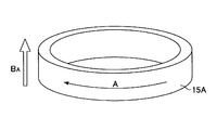
- the axial magnetic shield 12A When an axial magnetic field (B A ) is applied to the superconducting magnetic shield device 10A (see FIG. 6), the axial magnetic shield 12A functions. In other words, when an axial magnetic field (B A ) is applied, an eddy current A is generated in the circumferential direction in each of the axial tape-like superconducting materials 15A constituting the axial magnetic shield 12A, thereby causing an axial magnetic field (B A ). B A ) can be prevented from affecting the space portion 14.
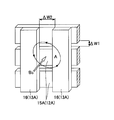
- the transverse magnetic shield 13A functions. That is, when the horizontal direction magnetic field (B S) is applied, axially tape-like superconducting material 15A and lateral tape-like superconducting material 16 as shown in FIG. 7, the horizontal direction magnetic field (B S) An eddy current A flowing in the circular direction around the application position is generated.
- the tape-like superconducting material 15A for the axial direction and the tape-like superconducting material 16 for the lateral direction are electrically connected by the solder 19 (see FIG. 5). Therefore, the eddy current A generated by the transverse magnetic field (B S ) flows inside each tape-shaped superconducting material 15, 16 or across each tape-shaped superconducting material 15, 16. Therefore, according to the superconducting magnetic shield device 10 ⁇ / b > A, it is possible to prevent the lateral magnetic field (B S ) from affecting the space portion 14.
- FIG. 8 shows the shield rate against the transverse magnetic field (B S ) of the superconducting magnetic shield device 10A.
- FIG. 9 shows the shielding rate against the axial magnetic field (B A ) of the superconducting magnetic shield device 10A. The characteristics shown in FIGS. 8 and 9 are all obtained by simulation.
- the horizontal axis is the frequency
- the vertical axis is the shield rate.
- the horizontal axis indicates the frequency for the following reason. That is, in the superconducting magnetic shield device 10A according to the present embodiment, the solder 18 is used to join both ends of the tape-like superconducting material 15A for the axial direction (see FIG. 4), and each of the tape-like superconducting materials 15 and 16 is attached. Solder 19 is also used for joining. That is, the axial magnetic shield 12A and the lateral magnetic shield 13A are not perfect superconductors but include the resistance components of the solders 18 and 19.
- the applied magnetic field is a DC magnetic field
- the axial magnetic shield 12A and the lateral magnetic shield 13A cannot effectively shield them.
- shielding can be performed. 8 to 10 show the frequency of the applied magnetic field as the horizontal axis.
- the frequency of the magnetic field is 1 Hz or more regardless of whether the magnetic field is an axial magnetic field or a longitudinal magnetic field. Therefore, when the shield rate at 1 Hz of the lateral external magnetic field (B S ) in FIG. 8 is seen, it can be seen that the shield rate of the transverse magnetic shield 13A is as high as about 7000. Further, in FIG. 9, when the shield rate at the axial external magnetic field (B A ) at 1 Hz is seen, it can be seen that the shield rate of the axial magnetic shield 12A is as high as about 12,500.
- the superconducting magnetic shield device 10 ⁇ / b> A is effective for both the axial magnetic field (B A ) and the lateral magnetic field (B S ) from the outside. Prove that you can make a good shield.
- the axial magnetic shield 12A is obtained by laminating the axial tape-like superconducting material 15A in the axial direction, and the lateral magnetic shield 13A is provided with the lateral tape-like superconducting material 16 arranged in the circumferential direction. It is a thing. That is, the axial magnetic shield 12A and the lateral magnetic shield 13A are not integrally molded, and a plurality of axial tape-like superconducting materials 15A and lateral tape-like superconducting materials 16 are assembled and joined together. Has been.
- the individual tape-like superconducting materials 15 and 16 can be inspected for quality when the axial magnetic shield 12A and the lateral magnetic shield 13A are manufactured.
- the axial magnetic shield 12A and the lateral magnetic shield 13A after selecting the good tape-shaped superconducting materials 15 and 16.
- the yield can be increased even when the high-temperature superconducting material is used.
- the gap ⁇ W1 inevitably between the adjacent axial tape-like superconducting materials 15A (FIG. 5, FIG. 5). 7 is indicated by an arrow).
- the lateral magnetic shield 13A is configured by arranging the lateral tape-shaped superconducting material 16 side by side, the gap ⁇ W2 inevitably between the adjacent lateral tape-shaped superconducting materials 16 (arrows in FIGS. 2 and 7). Occurs).
- FIG. 10A shows the distance ⁇ W1 between adjacent axial tape-like superconducting materials 15A, the connection resistance of the axial tape-like superconducting material 15A, and the shielding rate of the axial magnetic shield 12A in the axial magnetic shield 12A. Shows the relationship.
- FIG. 10B shows the distance ⁇ W2 between the adjacent lateral tape-shaped superconducting materials 16, the connection resistance of the lateral tape-shaped superconducting material 16, and the shield of the lateral magnetic shield 13A. The relationship with the rate is shown.
- connection resistance that is, the connection resistance of the solder 18
- the shield rate was set to be 1000 or more. That is, the connection resistance of the axial tape-like superconducting material 15A by the solder 18 was set to about 0.1 ⁇ .
- the gap between the axial tape-like superconducting materials 15A laminated in the axial direction was set to 2 mm or less.
- the connection resistance between the axial tape-shaped superconducting material 15A and the lateral tape-shaped superconducting material 16 is set to be equal to that of the lateral magnetic shield 13A.
- the shield rate was set to be 1000 or more. That is, the connection resistance by the solder 19 was set to about 0.1 ⁇ . Further, the gap between the transverse tape-like superconducting materials 16 arranged in parallel in the circumferential direction was set to 2 mm or less.
- the superconducting magnetic shield device 10A is applied to a weak magnetic field measuring device that measures a weak magnetic field such as a magnetoencephalograph or a magnetocardiograph, the external magnetic field can be reliably shielded. Can be accurately measured.
- 11 to 23 show superconducting magnetic shield devices 10B to 10F according to the second to seventh embodiments. 11 to 23, the components corresponding to those of the superconducting magnetic shield device 10A according to the first embodiment shown in FIGS. 1 to 7 are denoted by the same reference numerals, and the description thereof is omitted.
- FIG. 11 shows a superconducting magnetic shield device 10B according to the second embodiment.
- the tape-shaped superconducting material 16 for the lateral direction is arranged in parallel with the axial direction (arrow Z1, Z2 direction) is shown.
- the extending direction of the tape-shaped superconducting material 16 for the lateral direction (the directions of arrows D1 and D2 in the figure) is set in the axial direction (Z1, Z1) of the axial magnetic shield 12A. Z2 direction) was inclined.
- FIG. 11 shows an example in which the lateral tape-shaped superconducting material 16 is inclined at an angle ⁇ with respect to the axial direction.
- FIG. 12 shows a superconducting magnetic shield device 10C according to the third embodiment.
- the superconducting magnetic shield device 10A according to the first embodiment described above has a configuration in which the support 11A is disposed at the innermost peripheral position.
- the support 11B is disposed at the outermost peripheral position.
- the axial magnetic shield 12A is positioned on the innermost periphery
- the lateral magnetic shield 13A is positioned on the outer side
- the support 11B is positioned on the outermost periphery.
- a cooling pipe 17 through which a coolant for cooling the high-temperature superconducting material of the axial magnetic shield 12A and the lateral magnetic shield 13A flows is provided on the outer peripheral surface of the support 11B.
- the cooling pipe 17 is spirally disposed on the outer periphery of the support 11B.
- the cooling pipe 17 is not limited to this.
- the support 11B is disposed on the outermost periphery, and the magnetic shields 12 and 13 are protected by the support 11B because the axial magnetic shield 12A and the lateral magnetic shield 13A are located inside the support 11B. Therefore, even if an unnecessary external force is applied, the magnetic shields 12 and 13 can be prevented from being damaged.
- FIG. 13 is a plan view showing a superconducting magnetic shield device 10D according to the fourth embodiment.
- the plurality of transverse tape-like superconducting materials 16 constituting the transverse magnetic shield 13A are formed in an elongated plate shape and are not bent. It was.
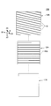
- a predetermined range predetermined range on the Z1 direction side
- a predetermined range on the Z1 direction side above the lateral tape-shaped superconducting material 20 constituting the lateral magnetic shield 13C is bent inward.
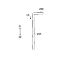
- FIG. 14 is an enlarged view of an example of one lateral tape-shaped superconducting material 20 constituting the superconducting magnetic shield device 10D according to the present embodiment.
- the tape-shaped superconducting material 20 for the lateral direction is configured to have a main body portion 20A and a bent portion 20B which is bent by bending the upper portion thereof. And has a substantially L-shape.
- the bent portion 20B in the lateral tape-shaped superconducting material 20 constituting the transverse magnetic shield 13C, a part of the upper opening of the superconducting magnetic shield device 10D is formed by the bent portion 20B.
- the configuration is closed.
- the shielding effect is greatly increased by covering part of the opening with a superconducting material. Therefore, according to the superconducting magnetic shield device 10D according to the present embodiment, the shielding effect can be further enhanced.
- the bending angle is not limited to the right angle shown in the figure, and can be set as appropriate.
- a plurality of axial tape-like superconducting materials 15A are stacked and arranged along the outer periphery of the support 11A so as to be juxtaposed in the axial direction.
- a plurality of lateral tape-like superconducting materials 16 constituting the lateral magnetic shield 13A are disposed on the outer periphery of the support 11A, and then the lateral tape.
- One tape-shaped superconducting material 15 ⁇ / b> B for axial direction is wound spirally around the superconducting material 16.
- the following method is conceivable as a method for mounting the individual tape-like superconducting material 15A for the axial direction on the support 11A.
- the tape-shaped superconducting material 21 is formed in a ring shape, and this is bonded and fixed to the support 11A over a predetermined range. Subsequently, both end portions of the tape-shaped superconducting material 21 are attached to each other, and the end portions are joined with the solder 18 (see FIG. 4).
- the axial magnetic shield 12A is composed of a single axial tape-shaped superconducting material 15B. Further, the length of the axial magnetic shield 12A is set to a length that allows the support 11A on which the transverse tape-shaped superconducting material 16 is disposed to be spirally wound a plurality of times. Therefore, the axial magnetic shield 12B is mounted on the support 11A by simply winding one axial tape-like superconducting material 15B around the support 11A on which the lateral tape-like superconducting material 16 is disposed. be able to.
- the number of parts can be reduced and the assembling work can be simplified.
- the axial magnetic shield 12B is formed of the single axial tape-like superconducting material 15B and spirally wound around the support 11A. It is good also as a structure which comprises this with the tape-shaped superconducting material for one horizontal direction, and winds this around the support body 11A helically.
- both the axial magnetic shield and the lateral magnetic shield may be formed of a single tape-shaped superconducting material, and both may be wound spirally around the support 11A. With this configuration, it is possible to further simplify the assembly work of the superconducting magnetic shield device.
- each of the axial magnetic shield and the lateral magnetic shield is constituted by one tape-shaped superconducting material.
- the axial magnetic shield and the lateral magnetic shield are composed of a plurality of tape-shaped superconducting materials. It is good also as a structure made into one by connecting.
- FIG. 17 is a plan view of the superconducting magnetic shield device 10F
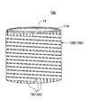
- FIG. 18 is a view showing a cross section of the axial magnetic shield 12A by cutting out a part of the superconducting magnetic shield device 10F.
- the support 11A is not shown.
- the gap between the axial tape-shaped superconducting material 15A constituting the axial magnetic shield 12A is set to 2 mm or less. However, there may be a case where it is necessary to perform a magnetic shield with higher accuracy.
- the superconducting magnetic shield device 10F closes the gap 34 formed between the axial tape-shaped superconducting materials 15A constituting the axial magnetic shield 12A with the closing magnetic shield 30 in order to cope with this. It is a configuration.
- the blocking magnetic shield 30 is disposed inside the axial magnetic shield 12A in this embodiment. However, it is also possible to dispose the closing magnetic shield 30 outside the axial magnetic shield 12A (on the side facing the lateral magnetic shield 13A).
- the closing magnetic shield 30 is composed of a plurality of closing tape-like superconducting materials 32.
- the closing tape-shaped superconducting material 32 the same configuration as the axial tape-shaped superconducting material 15A constituting the axial magnetic shield 12A can be used.
- the closing tape-shaped superconducting material 32 can be formed by bending the tape-shaped superconducting material 21 into a ring shape and joining both ends thereof with the solder 18.
- Each of the closing tape-like superconducting materials 32 constituting the closing magnetic shield 30 has a width (length in the Z1, Z2 direction) larger than the size of the gap 34 between the adjacent axial tape-like superconducting materials 15A. Yes. Further, each closing tape-shaped superconducting material 32 is configured to be electrically joined (for example, soldered) to the axial tape-shaped superconducting material 15A.
- FIG. 19 is a diagram showing the effect of the superconducting magnetic shield device 10F according to the present embodiment.
- the characteristics indicated by the arrow F are the same as the characteristics indicated by the arrow A in FIG. That is, the relationship between the connection resistance and the shield rate when the gap ⁇ W1 of the tape-like superconducting material 15A for the axial direction is 1 mm is shown. As described above, it can be understood that a high shielding effect can be obtained by setting the gap ⁇ W1 of the axial tape-like superconducting material 15A to 1 mm.
- an arrow E in the figure indicates the characteristic of the superconducting magnetic shield device 10F according to the present embodiment in which the gap 34 is closed by the closing magnetic shield 30. It can be seen that the characteristic of the superconducting magnetic shield device 10F is improved by about 10 compared to the characteristic when the gap ⁇ W1 of the axial tape-like superconducting material 15A is 1 mm.
- the superconducting magnetic shield device 10F according to the present embodiment, it is possible to realize high shielding performance while facilitating the assembly work.
- the configuration in which the blocking magnetic shield 30 covering the gap 34 formed in the axial magnetic shield 12A is provided.
- the horizontal tape-shaped superconducting material 16 between the horizontal magnetic shields 13A is provided.
- a closing tape-shaped superconducting material (corresponding to the second closing superconducting material described in the claims) may be disposed so as to close the gap formed by the step (shown by an arrow ⁇ W2 in FIG. 7).
- the closing tape-like superconducting material is formed so as to close only the gap 34 formed between the axial tape-like superconducting materials 15A, or is formed between the lateral tape-like superconducting materials 16.
- a configuration may be provided in which only the gap ( ⁇ W2) is closed, or a configuration in which both the gap 34 and the gap ( ⁇ W2) are further closed.
- the axial magnetic shield 12A is formed by disposing the axial tape-like superconducting material 15A on the support 11A, and then the lateral tape-like tape is formed on the axial magnetic shield 12A.
- the superconducting material 16 is soldered to join the transverse magnetic shield 13A, thereby producing the superconducting magnetic shield device 10A.
- the lattice-shaped magnetic shield 40 having a configuration in which the tape-shaped superconducting material 15A for the axial direction and the tape-shaped superconducting material 16 for the lateral direction are soldered in a lattice shape is manufactured in advance and supported.
- a superconducting magnetic shield device 10F was manufactured by disposing it on the body 11A.
- an example of the manufacturing method of the superconducting magnetic shield device 10F will be described.
- the tape-shaped superconducting materials 21 are arranged in the directions of arrows X1 and X2 in FIG. Subsequently, the tape-shaped superconducting material 21 is arranged in the directions of arrows Y1 and Y2 in FIG. 20 on the tape-shaped superconducting material 21 arranged in this manner.
- the tape-shaped superconducting materials 21 arranged in a row in the X1 and X2 directions constitute a tape-shaped superconducting material 16 for the horizontal direction, and the tape-shaped superconducting materials 21 arranged in a row in the Y1 and Y2 directions are shafts.
- a directional tape-shaped superconducting material 15A is formed. Further, when the tape-shaped superconducting material 21 to be the axial tape-shaped superconducting material 15 ⁇ / b> A is stacked on the tape-shaped superconducting material 21 to be the axial-shaped tape-shaped superconducting material 15 ⁇ / b> A, the tape-shaped superconducting material 21 intersects at a portion where the tape-shaped superconducting material 21 intersects.
- a high melting point solder is disposed.
- the tape-shaped superconducting materials 21 arranged in a grid are subjected to heat treatment in a heating furnace. Thereby, the high melting point solder is melted, and soldering is performed at each crossing portion of each tape-shaped superconducting material 21. Thereby, the tape-shaped superconducting material 15A for the axial direction and the tape-shaped superconducting material 16 for the lateral direction are joined, and the sheet-like lattice-shaped magnetic shield 40 is manufactured (electromagnetic shield forming step).
- the lattice-shaped magnetic shield 40 can be easily manufactured.
- the arrangement process can be performed on a plane such as a base. Therefore, compared with a method in which a large number of tape-like superconducting materials 15A for the axial direction and a tape-like superconducting material 16 for the lateral direction are arranged on the cylindrical support 11A, the process of bringing the tape-like superconducting materials 21 closer to each other is easier. Can be done.
- a gap between adjacent axial tape-like superconductors 15A and a gap between adjacent tape-like superconductors 16 for horizontal direction are widely illustrated.
- the dimension of is about 2mm.
- the lattice-shaped magnetic shield 40 manufactured as described above is mounted by being wound around a support 11A manufactured in advance (mounting process). At this time, the lattice-shaped magnetic shield 40 and the support 11A are fixed using an adhesive or the like.
- the tape-shaped superconducting material 21 is a bendable tape-shaped member, and the lattice-shaped magnetic shield 40 obtained by soldering the tape-shaped superconducting material 21 in a lattice shape is also flexible. Further, since the lattice-shaped magnetic shield 40 has a configuration in which the axial tape-shaped superconducting material 15A and the lateral tape-shaped superconducting material 16 are integrated, the axial tape-shaped superconducting material 15A and the lateral tape-shaped superconducting material 16 are integrated. 16 can be collectively wound around the support 11A.
- the process of mounting the lattice-shaped magnetic shield 40 on the support 11A can be easily performed.
- FIG. 22 shows a state in which both end portions (indicated by arrows P in the drawing) of the axial tape-shaped superconducting material 15A are abutted by the lattice-shaped magnetic shield 40 being wound around the support 11A.
- the axial tape-like superconducting material 15A needs to be electrically joined to effectively shield the axial magnetic field (see FIG. 4).
- solder 45 is disposed at the mating portions.
- the solder 45 is a low melting point solder having a lower melting point than that of the high melting point solder used to join the tape-shaped superconducting material 21 arranged in a grid pattern in the electromagnetic shield forming step.
- the solder 45 is melted to electrically join the butted portions of the tape-shaped superconducting materials 15A for each axial direction (joining step).
- the superconducting magnetic shield device 10G shown in FIG. 23 is manufactured.
- the lattice-shaped magnetic shield 40 can be easily manufactured in the electromagnetic shield forming step as described above. For this reason, it is possible to easily assemble the superconducting magnetic shield device 10G.
Landscapes
- Engineering & Computer Science (AREA)
- Microelectronics & Electronic Packaging (AREA)
- Containers, Films, And Cooling For Superconductive Devices (AREA)
- Measurement And Recording Of Electrical Phenomena And Electrical Characteristics Of The Living Body (AREA)
- Superconductor Devices And Manufacturing Methods Thereof (AREA)
- Shielding Devices Or Components To Electric Or Magnetic Fields (AREA)
Abstract
本発明は高温超電導材料を用いても組み立ての容易化、歩留まりの向上、及び低コスト化を図ることができる超電導磁気シールド装置に係り、周方向に配設された軸方向用超電導材からなる軸方向磁気シールドと、前記軸方向磁気シールドの軸方向に対して直交或いは傾いて配設され、前記軸方向磁気シールドと電気的に接続される横方向用超電導材からなる横方向磁気シールドと、前記軸方向磁気シールド及び前記横方向磁気シールドを支持する支持体とを備える。
Description
本発明は、高温超電導体を用いて磁気シールドを行う超電導磁気シールド装置及びその製造方法に関する。
例えば、脳磁計や心磁計のような微弱磁場を計測する微弱磁場計測装置は、地磁気等の外部磁場が印加された場合、これを外乱として計測してしまう。このため、外乱が微弱磁場計測装置に悪影響を及ぼさないように微弱磁場計測装置を外乱となる外部磁場から遮蔽する磁気シールド装置でシールドし、これにより微弱磁場を計測することが行われている。
従来、この磁気シールド装置としては、微弱磁場計測装置を設置する部屋の内壁全体を磁気シールド材で構成し、この磁気シールドルームにより外部磁場の影響を防止するものがあった(特許文献1参照)。しかしながら、磁気シールドルームは部屋全体を磁気シールドする構成であるため、大掛かりな設備となってしまう。
そこで、内部に人体全体或いは頭部を装着可能とした筒状の超電導磁気シールド装置が提案されている(特許文献2参照)。この超電導磁気シールド装置は筒状基材にマイスナー効果を有する超電導体を配設した構成を有し、地磁気等が印加された際に超電導体が有する完全反磁性により対象空間の磁場を遮蔽する。これにより、地磁気等の外部磁場に影響されることなく、微弱磁場を計測することが可能となる。
ところで、超電導磁気シールドを構成する超電導材としては、低温超電導材と高温超電導材が存在する。超電導磁気シールドの材料として低温超電導材を用いた場合、低温超電導材は成型が容易であるため大径の円筒形状を有した超電導磁気シールドを比較的容易に製造することかできる。しかしながら、低温超電導材料を用いた場合には冷却温度を9K以下に保つ必要があり、冷却装置が大掛かりになってしまう。
これに対し、超電導磁気シールドの材料として高温超電導材を用いた場合、冷却温度は80K以下と冷却は容易になるが、高温超電導材料は製造が面倒となる。具体的には、円筒状基材に溶射により高温超電導材料を被膜形成することが行われる。しかしながら、この作業は面倒で作製に長い時間を要し製品コストが高くなるという問題点がある。
一方、超電導磁気シールド装置は、筒状に形成された超電導磁気シールドの内部に人が入るため、これに対応した大きさが必要となる。これに対し、従来の高温超電導材料を用いた超電導磁気シールドは、一体物とされていたため部分補修ができなかった。
よって、超電導磁気シールドの一部に不良箇所が発生すると、大きな形状を有する超電導磁気シールドの全てが使用不可能となり、全体を改めて作製し直す必要が生ずる。このため、従来の超電導磁気シールド装置は歩留まりが低く、製造に関するリスクが高いという問題点があった。
更に、高温超電導材料は歪に対して脆弱であり、歪により容易にクラックが発生するため、超電導磁気シールド装置の組み立て作業においてその取扱に注意を要するという問題点もあった。
本発明は、上述した従来技術の問題を解決する、改良された有用な超電導磁気シールド装置及びその製造方法を提供することを総括的な目的とする。
本発明のより詳細な目的は、高温超電導材料を用いても組み立ての容易化、歩留まりの向上、及び低コスト化を図りうる超電導磁気シールド装置及びその製造方法を提供することにある。
この目的を達成するために、本発明は、
前記軸方向磁気シールドの軸方向に対して直交或いは傾いて配設され、前記軸方向磁気シールドと接続される横方向用超電導材からなる横方向磁気シールドと、
前記軸方向磁気シールド及び前記横方向磁気シールドを支持する支持体とを有する。
前記軸方向磁気シールドの軸方向に対して直交或いは傾いて配設され、前記軸方向磁気シールドと接続される横方向用超電導材からなる横方向磁気シールドと、
前記軸方向磁気シールド及び前記横方向磁気シールドを支持する支持体とを有する。
開示の発明によれば、軸方向磁気シールドと横方向磁気シールドとにより超電導磁気シールド装置が構成されているため、超電導磁気シールド装置の組み立ての容易化、歩留まりの向上、及び低コスト化を図ることができ、また軸方向磁場及び横方向磁場が印加されてもこれを確実にシールドすることができる。
10A~10G 超電導磁気シールド装置
11A,11B 支持体
12A,12B 軸方向磁気シールド
13A,13B,13C 横方向磁気シールド
14 空間部
15A,15B 軸方向用テープ状超電導材
16,20 横方向用テープ状超電導材
20A 本体部
20B 折曲部
17 冷却管
18,19 はんだ
30 閉塞用磁気シールド
32 閉塞用テープ状超電導材
34 間隙
40 格子状磁気シールド
11A,11B 支持体
12A,12B 軸方向磁気シールド
13A,13B,13C 横方向磁気シールド
14 空間部
15A,15B 軸方向用テープ状超電導材
16,20 横方向用テープ状超電導材
20A 本体部
20B 折曲部
17 冷却管
18,19 はんだ
30 閉塞用磁気シールド
32 閉塞用テープ状超電導材
34 間隙
40 格子状磁気シールド
以下、本発明の実施形態について図面を参照しつつ説明する。
なお、添付の全図面の中の記載で、同一又は対応する部材又は部品には、同一又は対応する参照符号を付し、重複する説明を省略する。また、図面は、特に指定しない限り、部材もしくは部品間の相対比を示すことを目的としない。従って、具体的な寸法は、以下の限定的でない実施形態に照らし、当業者により決定することができる。
また、以下説明する実施形態は、発明を限定するものではなく例示であって、実施形態に記述される全ての特徴やその組み合わせは、必ずしも発明の本質的なものであるとは限らない。
図1乃至図3は、本発明の第1実施形態である超電導磁気シールド装置10Aを示している。図1は超電導磁気シールド装置10Aの斜視図、図2は平面図、図3は分解斜視図である。この超電導磁気シールド装置10Aは、例えば脳磁計や心磁計のような微弱磁場を計測する微弱磁場計測装置に適用される。
超電導磁気シールド装置10Aは、支持体11A、軸方向磁気シールド12A、及び横方向磁気シールド13A等を有している。本実施形態では、最内周に支持体11Aが配設され、その外周に軸方向磁気シールド12Aが配設され、更にその外周に横方向磁気シールド13Aが配設された構成とされている。よって、超電導磁気シールド装置10Aは、支持体11A、軸方向磁気シールド12A、及び横方向磁気シールド13Aが三重に重なった構成とされている。
また、超電導磁気シールド装置10Aは、全体として円筒形状を有している。よって、その中央部分には空間部14が形成されており、超電導磁気シールド装置10Aを脳磁計に適用した場合には、この空間部14の内部に脳磁計が配設され、また被測定体となる人の頭部が挿入される。以下、超電導磁気シールド装置10Aを構成する各構成要素について説明する。
先ず、支持体11Aについて説明する。支持体11Aは円筒形状を有しており、軸方向磁気シールド12A及び横方向磁気シールド13Aを支持するものである。
この支持体11Aは、特にその材質を限定されるものではないが、本実施形態では非磁性で成形性の良好な樹脂或いは金属を用いている。具体的には、FRP(ガラス繊維強化プラスチック)等を用いることができる。また、この支持体11Aの内周に、各磁気シールド12,13Aを冷却する冷媒が流れる冷却管を配設してもよい。
軸方向磁気シールド12Aは、軸方向磁場に対するシールドを行うものである。なお、本明細書において、円筒の軸方向(図中矢印Z1,Z2で示す方向)の磁場を軸方向磁場と呼び、円筒の軸方向に直交する方向の磁場を横方向磁場と呼ぶものとする。また、軸方向磁場に対する磁気シールドを軸方向磁気シールドといい、横方向磁場に対する磁気シールドを横方向磁気シールドというものとする。
なお、軸方向又は横方向以外の方向から印される磁場は、軸方向の成分(軸方向磁場成分)と、横方向の成分(横方向磁場成分)とに分解することができる。このため、以下の説明においては軸方向磁場と横方向磁場についてのみ説明するものとする。
次に、軸方向磁気シールド12Aについて説明する。軸方向磁気シールド12Aは、軸方向用テープ状超電導材15Aを支持体11Aの軸方向に複数積層した(積み重ねた)構成を有している。軸方向用テープ状超電導材15Aは、図4に拡大して示すように、テープ状超電導材21を曲げてリング状にすると共に、その両端部をはんだ18で接合した構成としてもよい。
ここで、テープ状超電導材21としては、超電導材の外周を金属で覆うか、又は金属の基板の上に高温超電導材を成膜したものを用いることができる。また、超電導材としては、臨界温度が高い高温超電導材を用いている。このテープ状超電導材21としては、例えば住友電気工業株式会社製のDI-BSCCO(製品名)を用いることができる。
このように構成されたテープ状超電導材21は、超電導材単体の場合に比べて機械的強度が高く、歪に対しても強い。このため、図4に示すようにテープ状超電導材21をループ状に成形しても、その歪により高温超電導材が損傷するようなことはなく歩留まりの向上を図ることができる。また、テープ状超電導材21及び軸方向用テープ状超電導材15Aの取扱が容易であることにより、軸方向磁気シールド12Aの組み立て作業を容易に行うことができる。
上記の構成とされた軸方向用テープ状超電導材15Aは、支持体11Aの外周に接着剤等を用いて固定される。これにより、軸方向磁気シールド12Aは、支持体11Aに支持された構成となる。
次に、横方向磁気シールド13Aについて説明する。横方向磁気シールド13Aは、本実施形態では横方向用テープ状超電導材16を支持体11Aの周方向に複数並設した(平行に並べた)構成を有している。この横方向用テープ状超電導材16は、上記したテープ状超電導材21と同様に、高温超電導材の外周を金属で覆うか、又は金属の基板の上に高温超電導材を成膜した構成のものを使用することができる。
横方向磁気シールド13Aは、軸方向磁気シールド12Aと異なり直線状とされている。よって、軸方向磁気シールド12Aと横方向磁気シールド13Aは、図1及び図7に示すように、互いに直交する方向に延在した構成となっている。
また本実施形態では、各々の横方向用テープ状超電導材16の長手方向が軸方向と平行なるよう構成されている。更に横方向用テープ状超電導材16は、筒状とされた軸方向磁気シールド12Aの外周位置を囲うように配設されている。
各横方向用テープ状超電導材16は、図5に拡大して示すように、各軸方向磁気シールド12Aを構成する軸方向用テープ状超電導材15Aに例えばはんだ19を用いて接合されることにより電気的に接続されている。即ち、軸方向用テープ状超電導材15Aと横方向用テープ状超電導材16は、はんだ19等により電気的に接続される。
次に、上記構成とされた超電導磁気シールド装置10Aにおいて、外部から磁場が印加された時の動作について説明する。
超電導磁気シールド装置10Aに対して軸方向磁場(BA)が印加された場合(図6参照)は、軸方向磁気シールド12Aが機能する。即ち、軸方向磁場(BA)が印加された場合は、軸方向磁気シールド12Aを構成する各軸方向用テープ状超電導材15Aに周方向に渦電流Aが発生し、これにより軸方向磁場(BA)が空間部14内に影響することを防止できる。
これに対し、超電導磁気シールド装置10Aに対して横方向磁場(BS)が印加された場合(図7参照)は、横方向磁気シールド13Aが機能する。即ち、横方向磁場(BS)が印加された場合は、図7に示すように軸方向用テープ状超電導材15A及び横方向用テープ状超電導材16内に、横方向磁場(BS)の印加位置を中心として円方向に流れる渦電流Aが発生する。
前記のように、軸方向用テープ状超電導材15Aと横方向用テープ状超電導材16ははんだ19で電気的に接続されている(図5参照)。よって、横方向磁場(BS)で発生する渦電流Aは各テープ状超電導材15,16の内部或いは各テープ状超電導材15,16を跨いで流れる。よって、超電導磁気シールド装置10Aによれば、横方向磁場(BS)が空間部14内に影響することを防止できる。
図8は、超電導磁気シールド装置10Aの横方向磁場(BS)に対するシールド率を示している。また図9は、超電導磁気シールド装置10Aの軸方向磁場(BA)に対するシールド率を示している。図8及び図9に示す特性は、いずれもシミュレーションにより求めたものである。
各図において、横軸は周数であり、縦軸はシールド率である。ここで、シールド率とは、超電導磁気シールド装置10Aの空間部14内の磁場の強さ(BIN)に対する外部の磁場BOUTの強さの比をいう(シールド率=BOUT/BIN)。
なお図8、図9、及び後述する図10において、横軸に周波数を取っているのは次の理由による。即ち、本実施形態に係る超電導磁気シールド装置10Aは、軸方向用テープ状超電導材15Aの両端部を接合するのにはんだ18を用い(図4参照)、また各テープ状超電導材15,16を接合するのにもはんだ19を用いている。即ち、軸方向磁気シールド12A及び横方向磁気シールド13Aは完全な超電導体ではなく、はんだ18,19の抵抗成分を含んだものである。
このため、印加される磁場が直流的な磁場である場合には、軸方向磁気シールド12A及び横方向磁気シールド13Aはこれを有効にシールドすることができない。しかしながら、印加される磁場が交流的な磁場である場合には、シールドを行うことができる。そこで、図8~図10は、横軸として印加される磁場の周波数を取っている。
一般に、脳磁計や心磁計のような微弱磁場を計測する場合、軸方向磁場及び縦方向磁場のいずれの磁場であっても、磁場の周波数は1Hz以上を計測する。そこで、図8で横方向の外部磁場(BS)が1Hzにおけるシールド率を見ると、横方向磁気シールド13Aのシールド率は約7000と高い値となっていることが判る。また、図9で軸方向の外部磁場(BA)が1Hzにおけるシールド率を見ると、軸方向磁気シールド12Aのシールド率は約12500と高い値となっていることが判る。
よって、図8及び図9に示す結果より、本実施形態に係る超電導磁気シールド装置10Aによれば、外部からの軸方向磁場(BA)及び横方向磁場(BS)の双方に対して有効なシールドを行うことができることが証明された。
一方、前記のように軸方向磁気シールド12Aは軸方向用テープ状超電導材15Aを軸方向に積層したものであり、横方向磁気シールド13Aは横方向用テープ状超電導材16を周方向に並設したものである。即ち、軸方向磁気シールド12A及び横方向磁気シールド13Aは一体成形されたものではなく、軸方向用テープ状超電導材15A及び横方向用テープ状超電導材16を複数集合させ、これを接合した構成とされている。
更に、個々のテープ状超電導材15,16は、軸方向磁気シールド12A及び横方向磁気シールド13Aの作製時において良否検査が可能である。
よって本実施形態では、良品であるテープ状超電導材15,16を選定した上で、軸方向磁気シールド12A及び横方向磁気シールド13Aを作製することが可能となる。これにより本実施形態に係る超電導磁気シールド装置10Aによれば、高温超電導材を用いても歩留まりを高めることができる。
ところで、本実施形態のように軸方向用テープ状超電導材15Aを積層した構成の軸方向磁気シールド12Aでは、隣接する軸方向用テープ状超電導材15A間に必然的に間隙ΔW1(図5,図7に矢印で示す)が発生する。同様に、横方向磁気シールド13Aを横方向用テープ状超電導材16を並設した構成とすると、隣接する横方向用テープ状超電導材16間に必然的に間隙ΔW2(図2,図7に矢印で示す)が発生する。
図10(A)は、軸方向磁気シールド12Aにおいて、隣接する軸方向用テープ状超電導材15Aの距離ΔW1と、軸方向用テープ状超電導材15Aの接続抵抗と、軸方向磁気シールド12Aのシールド率との関係を示している。
図10(A)において、矢印Aで示す特性はΔW1=1mmの時のシールド率と接続抵抗との関係を示し、矢印Bで示す特性はΔW1=2mmの時のシールド率と接続抵抗との関係を示し、矢印Cで示す特性はΔW1=3mmの時のシールド率と接続抵抗との関係を示し、更に矢印Dで示す特性はΔW1=4mmの時のシールド率と接続抵抗との関係を示している。
また図10(B)は、横方向磁気シールド13Aにおいて、隣接する横方向用テープ状超電導材16の距離ΔW2と、横方向用テープ状超電導材16の接続抵抗と、横方向磁気シールド13Aのシールド率との関係を示している。
図10(B)において、矢印Aで示す特性はΔW2=1mmの時のシールド率と接続抵抗との関係を示し、矢印Bで示す特性はΔW2=2mmの時のシールド率と接続抵抗との関係を示し、矢印Cで示す特性はΔW2=3mmの時のシールド率と接続抵抗との関係を示し、更に矢印Dで示す特性はΔW2=4mmの時のシールド率と接続抵抗との関係を示している。
図10(A)及び図10(B)の結果より、軸方向磁気シールド12A及び横方向磁気シールド13Aのいずれにおいても、似た特性が得られた。即ち、軸方向磁気シールド12A及び横方向磁気シールド13Aのいずれにおいても、隣接する軸方向用テープ状超電導材15A,16間の間隙ΔW1,ΔW2が小さくなるに従いシールド率が良好になることが判った。また、軸方向磁気シールド12A及び横方向磁気シールド13Aのいずれにおいても、接続抵抗が小さいほど、シールド率が良好になることが判った。
本実施形態に係る超電導磁気シールド装置10Aでは、軸方向磁気シールド12Aを構成する各軸方向用テープ状超電導材15Aの両端部の接続抵抗(即ち、はんだ18の接続抵抗)を軸方向磁気シールド12Aのシールド率が1000以上となるよう設定した。即ち、軸方向用テープ状超電導材15Aのはんだ18による接続抵抗を約0.1Ωに設定した。また、軸方向に積層された軸方向用テープ状超電導材15Aの間隙を2mm以下とした。
このように各値を設定することにより、超電導磁気シールド装置10Aを脳磁計や心磁計のような微弱磁場を計測する微弱磁場計測装置に適用しても、外部磁場を確実にシールドでき、これらの計測を正確に行うことが可能となる。
同様に、軸方向磁気シールド12Aと横方向磁気シールド13Aとの電気的接続については、軸方向用テープ状超電導材15Aと横方向用テープ状超電導材16との接続抵抗を横方向磁気シールド13Aのシールド率が1000以上となるよう設定した。即ち、はんだ19による接続抵抗を約0.1Ωに設定した。また、周方向に並設された横方向用テープ状超電導材16の間隙を2mm以下とした。
このように各値を設定することによっても、超電導磁気シールド装置10Aを脳磁計や心磁計のような微弱磁場を計測する微弱磁場計測装置に適用しても、外部磁場を確実にシールドでき、これらの計測を正確に行うことが可能となる。
次に、本発明の第2乃至第7実施形態について説明する。
図11乃至図23は、第2乃至第7実施形態に係る超電導磁気シールド装置10B~10Fを示している。なお、図11乃至図23において、図1乃至図7に示した第1実施形態に係る超電導磁気シールド装置10Aの構成と対応する構成については同一符号を付してその説明を省略する。
図11は、第2実施形態である超電導磁気シールド装置10Bを示している。
前記した第1実施形態である超電導磁気シールド装置10Aは、横方向用テープ状超電導材16が軸方向(矢印Z1,Z2方向)と平行に配設した例を示した。これに対して本実施形態に係る超電導磁気シールド装置10Bは、横方向用テープ状超電導材16の延在方向(図中、矢印D1,D2方向)を軸方向磁気シールド12Aの軸方向(Z1,Z2方向)に対して傾いて配設した。
図11では、横方向用テープ状超電導材16を軸方向に対して角度θ傾けた例を示している。このように、軸方向に対する横方向用テープ状超電導材16の延出方向は平行(θ=0°)に限定されるものではなく、任意の角度に適宜変更が可能なものである。この構成とした場合でも、前記した第1実施形態と同様の効果を得ることができる。
図12は、第3実施形態である超電導磁気シールド装置10Cを示している。
前記した第1実施形態に係る超電導磁気シールド装置10Aは、支持体11Aを最内周位置に配置した構成を示した。これに対して本実施形態に係る超電導磁気シールド装置10Cは、支持体11Bを最外周位置に配設したものである。
即ち、本実施形態に係る超電導磁気シールド装置10Cでは、最内周に軸方向磁気シールド12Aが位置し、その外側に横方向磁気シールド13Aが位置し、最外周に支持体11Bが位置した構成とされている。このように、支持体11Bが最外周位置に配設されても、軸方向磁気シールド12A及び横方向磁気シールド13Aはこの支持体11Bにより支持される。
また、支持体11Bの外周面には、軸方向磁気シールド12A及び横方向磁気シールド13Aの高温超電導材を冷却する冷媒が流れる冷却管17が配設されている。この冷却管17は、図12に示す例では支持体11Bの外周に螺旋状に配設されているが、これに限定されるものではない。
本実施形態のように支持体11Bが最外周に配設され、軸方向磁気シールド12A及び横方向磁気シールド13Aがその内部に位置することにより、各磁気シールド12,13は支持体11Bにより保護されるため、不要な外力が印加されても磁気シールド12,13が損傷することを防止できる。
図13は、第4実施形態である超電導磁気シールド装置10Dを示す平面図である。
前記した第1実施形態に係る超電導磁気シールド装置10Aは、横方向磁気シールド13Aを構成する複数の横方向用テープ状超電導材16は、細長い板状の形状とされており、折り曲げられてはいなかった。これに対して本実施形態に係る超電導磁気シールド装置10Dでは、横方向磁気シールド13Cを構成する横方向用テープ状超電導材20の上方の所定範囲(Z1方向側の所定範囲)を内側に折曲した構成とした。
図14は、本実施形態に係る超電導磁気シールド装置10Dを構成する一つの横方向用テープ状超電導材20の一例を拡大して示している。同図に示すように、横方向用テープ状超電導材20は、その上部を折曲されることにより本体部20Aと、折り曲げられた折曲部20Bとを有した構成とされており、全体して略L字形状を有している。
このように、横方向磁気シールド13Cを構成する横方向用テープ状超電導材20に折曲部20Bを形成することにより、超電導磁気シールド装置10Dの上側の開口部の一部は折曲部20Bにより塞がれた構成となる。円筒状の超電導磁気シールドにおいて、開口部の一部を超電導材で覆うことによりシールド効果は大きく増大する。よって、本実施形態に係る超電導磁気シールド装置10Dによれば、更にシールド効果を高めることができる。なお、折り曲げ角度は、図示される直角に限定されるものではなく、適宜設定することが可能である。
図15及び図16は、第5実施形態である超電導磁気シールド装置10Eを示している。
前記した第1実施形態に係る超電導磁気シールド装置10Aは、支持体11Aの外周に沿って複数の軸方向用テープ状超電導材15Aを軸方向に並設されるよう積み重ねて配設していた。これに対して本実施形態に係る超電導磁気シールド装置10Eは、支持体11Aの外周に横方向磁気シールド13Aを構成する横方向用テープ状超電導材16を複数配設した後、この横方向用テープ状超電導材16上に1本の軸方向用テープ状超電導材15Bを螺旋状に巻回した構成としている。
図1乃至図3に示した超電導磁気シールド装置10Aの場合、個々の軸方向用テープ状超電導材15Aを支持体11Aに装着する方法としては、次の方法が考えられる。
先ず、テープ状超電導材21をリング状に形成し、これを支持体11Aに所定範囲にわたり接着固定する。続いて、テープ状超電導材21の両端部を付き合わせ、この端部同士をはんだ18で接合する(図4参照)。
これに対して本実施形態に係る超電導磁気シールド装置10Eは、軸方向磁気シールド12Aを一本の軸方向用テープ状超電導材15Bにより構成している。また、軸方向磁気シールド12Aの長さは、横方向用テープ状超電導材16が配設された支持体11Aを複数回にわたり螺旋状に巻回できる長さに設定されている。よって、単に1本の軸方向用テープ状超電導材15Bを横方向用テープ状超電導材16が配設された支持体11Aに巻回することにより、軸方向磁気シールド12Bを支持体11Aに装着することができる。
この際、軸方向磁気シールド12Bの内側面には、予めペースト状のはんだを塗布しておく。そして、この状態で軸方向磁気シールド12Bが巻回された支持体11Aを加熱炉で加熱しはんだを溶融することにより、一括的に軸方向磁気シールド12Bを横方向用テープ状超電導材16に電気的及び機械的に接合することができる。
よって、本実施形態に係る超電導磁気シールド装置10Eによれば、部品点数の削減を図れると共に、組み立て作業の簡単化を図ることができる。
なお、上記の説明では軸方向磁気シールド12Bのみを1本の軸方向用テープ状超電導材15Bにより形成し、これを支持体11Aに螺旋状に巻回した例を示したが、横方向磁気シールドを1本の横方向用テープ状超電導材で構成し、これを支持体11Aに螺旋状に巻回する構成する構成としてもよい。
また、軸方向磁気シールド及び横方向磁気シールドの双方を1本のテープ状超電導材で構成し、いずれも支持体11Aに対して螺旋状に巻回する構成とすることも可能である。この構成することにより、更に超電導磁気シールド装置の組み立て作業の簡単化を図ることができる。
更に、上記した例では軸方向磁気シールド及び横方向磁気シールドの夫々を1本のテープ状超電導材で構成した例を示したが、軸方向磁気シールド及び横方向磁気シールドは複数のテープ状超電導材を繋ぎ合わせることにより1本とした構成としてもよい。
図17及び図18は、第6実施形態である超電導磁気シールド装置10Fを示している。
なお、図17は超電導磁気シールド装置10Fの平面図であり、図18は超電導磁気シールド装置10Fの一部を切り欠くことにより、軸方向磁気シールド12Aの断面を示す図である。また図18においては、支持体11Aの図示は省略している。
前記したように、脳磁計や心磁計のような微弱磁場を計測する微弱磁場計測装置に超電導磁気シールド装置を適用する場合、軸方向磁気シールド12Aを構成する軸方向用テープ状超電導材15Aの間隙、及び横方向磁気シールド13Aを構成する横方向用テープ状超電導材16の間隙を2mm以下に設定することが望ましい。しかしながら、更に高精度の磁気シールドを行う必要が生じる場合が考えられる。
本実施形態に係る超電導磁気シールド装置10Fは、これに対応するために軸方向磁気シールド12Aを構成する軸方向用テープ状超電導材15Aの間に形成される間隙34を閉塞用磁気シールド30で塞ぐ構成としたものである。
閉塞用磁気シールド30は、本実施形態では軸方向磁気シールド12Aの内側に配設されている。しかしながら、閉塞用磁気シールド30を軸方向磁気シールド12Aの外側(横方向磁気シールド13Aと対向する側)に配設することも可能である。
閉塞用磁気シールド30は、複数の閉塞用テープ状超電導材32により構成されている。この閉塞用テープ状超電導材32は、軸方向磁気シールド12Aを構成する軸方向用テープ状超電導材15Aと同一構成のものを用いることができる。即ち、閉塞用テープ状超電導材32は、図4に示したように、テープ状超電導材21を曲げてリング状にすると共に、その両端部をはんだ18で接合したものを用いることができる。
閉塞用磁気シールド30を構成する各閉塞用テープ状超電導材32は、隣接する軸方向用テープ状超電導材15Aの間隙34の大きさよりも大きな幅(Z1,Z2方向の長さ)を有している。また、各閉塞用テープ状超電導材32は、軸方向用テープ状超電導材15Aに電気的に接合(例えば、はんだ付け)された構成とされている。
このように間隙34を閉塞用磁気シールド30で塞ぐことにより、前記の超電導磁気シールド装置10Aに比べ、更に外部磁場が空間部14内に進入することを防止することができる。
図19は、本実施形態に係る超電導磁気シールド装置10Fの効果を示す図である。
同図において、矢印Fで示すのは図10に矢印Aで示した特性と同じである。即ち、軸方向用テープ状超電導材15Aの間隙ΔW1を1mmとした時の接続抵抗とシールド率との関係を示している。前記したように、軸方向用テープ状超電導材15Aの間隙ΔW1を1mmとすることにより、高いシールド効果が得られることが分かる。
これに対して図中矢印Eで示すのは、間隙34を閉塞用磁気シールド30で塞いだ本実施形態に係る超電導磁気シールド装置10Fの特性を示している。超電導磁気シールド装置10Fの特性は、軸方向用テープ状超電導材15Aの間隙ΔW1を1mmとした時の特性に比べてシールド率が約10程度向上していることが分かる。
よって、軸方向用テープ状超電導材15A間に形成される間隙34を塞ぐ閉塞用磁気シールド30を設けることにより、高いシールド効果が得られることが実証された。
なお、本実施形態のように高いシールド効果を得る方法として、軸方向磁気シールド12Aを形成する際に、隣接する軸方向用テープ状超電導材15Aの間隙ΔWがなくなるよう(ΔW=0となるよう)、軸方向用テープ状超電導材15Aを支持体11Aに配設することも考えられる。
しかしながら、多数の軸方向用テープ状超電導材15Aをリング状に成形しつつ、かつ隣接する間隙ΔWがなくなるよう支持体11Aに配設する作業は困難で手間の掛かる作業となる。これに対し、閉塞用テープ状超電導材32により間隙34を塞ぐ作業は容易であり、かつ閉塞用テープ状超電導材32が間隙34を塞ぐことができれば、閉塞用テープ状超電導材32が上下方向(Z1,Z2方向)に若干ずれたとしても高いシールド性は維持される。
よって、本実施形態に係る超電導磁気シールド装置10Fによれば、組み立て作業の容易化を図りつつ、高いシールド性を実現することができる。
なお上記した実施形態では、軸方向磁気シールド12Aに形成される間隙34を覆う閉塞用磁気シールド30を設ける構成を示したが、横方向磁気シールド13Aを構成する横方向用テープ状超電導材16間に形成される間隙(図7に矢印ΔW2で示す)を塞ぐように閉塞用テープ状超電導材(請求項に記載の第2の閉塞用超電導材に相当する)を配設する構成としてもよい。
このように、閉塞用テープ状超電導材は、軸方向用テープ状超電導材15A間に形成される間隙34をのみ塞ぐように設けても、また横方向用テープ状超電導材16間に形成される間隙(ΔW2)のみを塞ぐように設けても、更に間隙34及び間隙(ΔW2)の双方を塞ぐように設けた構成としてもよい。
図20乃至図23は、第7実施形態である超電導磁気シールド装置10G及びその製造方法を示している。
前記した第1実施形態では、支持体11Aに軸方向用テープ状超電導材15Aを配設することにより軸方向磁気シールド12Aを形成し、その後に軸方向磁気シールド12Aの上部に横方向用テープ状超電導材16をはんだ付けすることにより横方向磁気シールド13Aを接合し、これにより超電導磁気シールド装置10Aを製造していた。
これに対して本実施形態では、軸方向用テープ状超電導材15Aと横方向用テープ状超電導材16を格子状にはんだ付けした構成の格子状磁気シールド40を予め製造しておき、これを支持体11Aに配設することにより超電導磁気シールド装置10Fを製造した。以下、超電導磁気シールド装置10Fの製造方法の一例について説明する。
超電導磁気シールド装置10Fを製造するには、先ずテープ状超電導材21を図20に矢印X1,X2方向に列設する。続いて、この列設されたテープ状超電導材21上に、テープ状超電導材21を図20に矢印Y1,Y2方向に列設する。
このX1,X2方向に列設に列設されたテープ状超電導材21は横方向用テープ状超電導材16を構成し、Y1,Y2方向に列設に列設されたテープ状超電導材21は軸方向用テープ状超電導材15Aを構成する。また、軸方向用テープ状超電導材15Aとなるテープ状超電導材21上に軸方向用テープ状超電導材15Aとなるテープ状超電導材21を重ねる際、各テープ状超電導材21が交差する部位には高融点はんだを配設しておく。
格子状に配列されたテープ状超電導材21は加熱炉において加熱処理が行われる。これにより高融点はんだは溶融し、各テープ状超電導材21の各交差部分においてははんだ付けが行われる。これにより、軸方向用テープ状超電導材15Aと横方向用テープ状超電導材16は接合され、シート状の格子状磁気シールド40が製造される(電磁シールド形成工程)。
上記のテープ状超電導材21をX1,X2方向及びY1,Y2方向に列設させる処理は容易であり、また多数の交差部におけるはんだ付けを行う処理も一括的に行うため容易である。よって、格子状磁気シールド40の製造を容易に行うことができる。
また電磁シールド形成工程においてテープ状超電導材21を格子状に列設する際、本実施形態では基台等の平面上で列設処理を行うことができる。よって、円筒形状の支持体11Aに対して多数の軸方向用テープ状超電導材15A及び横方向用テープ状超電導材16を配設する方法に比べ、各テープ状超電導材21を近接させる処理を容易に行うことができる。
なお、各図においては図示の便宜上、隣接する軸方向用テープ状超電導材15A間の間隙、及び隣接する横方向用テープ状超電導材16間の間隙を広く図示しているが、各間隙の実際の寸法は2mm程度とされている。
上記のように製造された格子状磁気シールド40は、図21に示されるように、予め製造されていた支持体11Aに巻き付けることにより装着される(装着工程)。この際、格子状磁気シールド40と支持体11Aは、接着剤等を用いて固定される。
テープ状超電導材21は曲げることが可能なテープ状の部材であり、これを格子状にはんだ付けした格子状磁気シールド40も可撓性を有している。また、格子状磁気シールド40は軸方向用テープ状超電導材15Aと横方向用テープ状超電導材16が一体化した構成であるため、軸方向用テープ状超電導材15Aと横方向用テープ状超電導材16を一括的に支持体11Aに巻き付けることができる。
よって本実施形態では、格子状磁気シールド40を支持体11Aに装着する処理を容易に行うことがきる。
図22は、格子状磁気シールド40が支持体11Aに巻き付けられることにより、軸方向用テープ状超電導材15Aの両端部(図中、矢印Pで示す)が突き合わされた状態を示している。軸方向用テープ状超電導材15Aは、軸方向磁場を有効にシールドするために電気的に接合する必要がある(図4参照)。
この各軸方向用テープ状超電導材15Aの端部Pを電気的に接合するため、このつき合わせ部分にはんだ45を配設する。このはんだ45は、電磁シールド形成工程において格子状に配置されたテープ状超電導材21を接合するのに用いた高融点はんだに比べ、融点が低い低融点はんだを用いている。
次に、加熱処理を行うことにより、はんだ45を溶融して各軸方向用テープ状超電導材15Aの突き合わせ部分を電気的に接合する(接合工程)。上記の処理を行うことにより、図23に示す超電導磁気シールド装置10Gが製造される。
本実施形態に係る製造方法では、上記のように電磁シールド形成工程において格子状磁気シールド40を容易に製造することができる。このため、超電導磁気シールド装置10Gの組み立て作業を容易に行うことが可能となる。
以上、本発明の好ましい実施形態について詳述したが、本発明は上記した特定の実施形態に限定されるものではなく、請求の範囲に記載された本発明の要旨の範囲内において、種々の変形・変更が可能なものである。
本国際出願は2013年3月5日に出願された日本国特許出願2013-043293号に基づく優先権を主張するものであり、日本特許出願2013-043293号の全内容をここに本国際出願に援用する。
Claims (10)
- 周方向に配設された軸方向用超電導材からなる軸方向磁気シールドと、
前記軸方向磁気シールドの軸方向に対して直交或いは傾いて配設され、前記軸方向磁気シールドと電気的に接続される横方向用超電導材からなる横方向磁気シールドと、
前記軸方向磁気シールド及び前記横方向磁気シールドを支持する支持体と、
を有する超電導磁気シールド装置。 - 前記軸方向用超電導材及び前記横方向用超電導材は、高温超電導材であることを特徴とする請求項1記載の超電導磁気シールド装置。
- 前記軸方向用超電導材及び前記横方向用超電導材は、テープ状超電導材であることを特徴とする請求項1記載の超電導磁気シールド装置。
- 前記軸方向磁気シールドは、前記軸方向用超電導材を前記軸方向に複数積層した構成であることを特徴とする請求項1記載の超電導磁気シールド装置。
- 前記横方向磁気シールドは、前記横方向用超電導材を前記周方向に複数並設した構成であることを特徴とする請求項1記載の超電導磁気シールド装置。
- 前記支持体を、接合された前記軸方向磁気シールドと前記横方向磁気シールドとの最外周位置又は最内周位置に配設したことを特徴とする請求項1記載の超電導磁気シールド装置。
- 前記軸方向磁気シールド又は前記横方向磁気シールドの少なくとも一方は、1本の前記軸方向用超電導材又は1本の前記横方向用超電導材を螺旋状に巻回した構成であることを特徴とする請求項1記載の超電導磁気シールド装置。
- 前記軸方向磁気シールドを構成する複数の前記軸方向用超電導材の間に形成される間隙を塞ぐ第1の閉塞用超電導材を設けたことを特徴とする請求項4記載の超電導磁気シールド装置。
- 前記横方向磁気シールドを構成する複数の前記軸方向用超電導材の間に形成される間隙を塞ぐ第2の閉塞用超電導材を設けたことを特徴とする請求項5記載の超電導磁気シールド装置。
- 周方向に延在するよう形成されたテープ状の軸方向用超電導材と、軸方向に対して直交或いは傾いて配設されると共に前記軸方向用超電導材と電気的に接続されるテープ状の横方向用超電導材と、前記軸方向用超電導材及び前記横方向用超電導材を支持する支持体とを有する超電導磁気シールド装置の製造方法であって、
複数の前記軸方向用超電導材と複数の前記横方向用超電導材を格子状に配置すると共に、前記軸方向用超電導材と前記横方向用超電導材の交差する部位を第1の導電性接合材で接合し電磁シールドを形成する電磁シールド形成工程と、
前記電磁シールドを前記支持体に巻き付ける装着工程と、
前記軸方向用超電導材の端部を前記第1の導電性接合材よりも接合温度が低い第2の導電性接合材で接合する接合工程と
を有することを特徴とする超電導磁気シールド装置の製造方法。
Applications Claiming Priority (2)
| Application Number | Priority Date | Filing Date | Title |
|---|---|---|---|
| JP2013-043293 | 2013-03-05 | ||
| JP2013043293A JP6211277B2 (ja) | 2012-04-26 | 2013-03-05 | 脳磁計用超電導磁気シールド装置及びその製造方法 |
Publications (1)
| Publication Number | Publication Date |
|---|---|
| WO2014136288A1 true WO2014136288A1 (ja) | 2014-09-12 |
Family
ID=51492119
Family Applications (1)
| Application Number | Title | Priority Date | Filing Date |
|---|---|---|---|
| PCT/JP2013/071403 Ceased WO2014136288A1 (ja) | 2013-03-05 | 2013-08-07 | 超電導磁気シールド装置及びその製造方法 |
Country Status (2)
| Country | Link |
|---|---|
| JP (1) | JP6211277B2 (ja) |
| WO (1) | WO2014136288A1 (ja) |
Families Citing this family (2)
| Publication number | Priority date | Publication date | Assignee | Title |
|---|---|---|---|---|
| CN104093297A (zh) * | 2014-06-13 | 2014-10-08 | 中国科学院等离子体物理研究所 | 一种磁屏蔽设备 |
| JP6951235B2 (ja) * | 2017-12-21 | 2021-10-20 | 住友重機械工業株式会社 | 超伝導磁気シールド装置、及び脳磁計装置 |
Citations (5)
| Publication number | Priority date | Publication date | Assignee | Title |
|---|---|---|---|---|
| JPH01152696A (ja) * | 1987-12-09 | 1989-06-15 | Toshiba Corp | 超電導部材 |
| JPH0289399A (ja) * | 1988-04-21 | 1990-03-29 | Kyushu Univ | 磁気シールド法 |
| JPH06216565A (ja) * | 1993-01-19 | 1994-08-05 | Koatsu Gas Kogyo Co Ltd | 帯状超電導シートから形成された超電導磁気遮蔽体 |
| JPH06224036A (ja) * | 1993-01-21 | 1994-08-12 | Koatsu Gas Kogyo Co Ltd | 外部磁気漏洩防止用の超電導磁気遮蔽体 |
| JP2009260363A (ja) * | 2009-06-15 | 2009-11-05 | Nippon Steel Corp | 磁気シールド装置 |
Family Cites Families (1)
| Publication number | Priority date | Publication date | Assignee | Title |
|---|---|---|---|---|
| JP2000021621A (ja) * | 1998-06-29 | 2000-01-21 | Railway Technical Res Inst | 超電導磁石の変動磁界シールド方法 |
-
2013
- 2013-03-05 JP JP2013043293A patent/JP6211277B2/ja active Active
- 2013-08-07 WO PCT/JP2013/071403 patent/WO2014136288A1/ja not_active Ceased
Patent Citations (5)
| Publication number | Priority date | Publication date | Assignee | Title |
|---|---|---|---|---|
| JPH01152696A (ja) * | 1987-12-09 | 1989-06-15 | Toshiba Corp | 超電導部材 |
| JPH0289399A (ja) * | 1988-04-21 | 1990-03-29 | Kyushu Univ | 磁気シールド法 |
| JPH06216565A (ja) * | 1993-01-19 | 1994-08-05 | Koatsu Gas Kogyo Co Ltd | 帯状超電導シートから形成された超電導磁気遮蔽体 |
| JPH06224036A (ja) * | 1993-01-21 | 1994-08-12 | Koatsu Gas Kogyo Co Ltd | 外部磁気漏洩防止用の超電導磁気遮蔽体 |
| JP2009260363A (ja) * | 2009-06-15 | 2009-11-05 | Nippon Steel Corp | 磁気シールド装置 |
Also Published As
| Publication number | Publication date |
|---|---|
| JP2013251527A (ja) | 2013-12-12 |
| JP6211277B2 (ja) | 2017-10-11 |
Similar Documents
| Publication | Publication Date | Title |
|---|---|---|
| JP6507312B2 (ja) | Hts磁石セクション | |
| TWI766229B (zh) | 電磁場遮蔽構造,其製造方法,及半導體製造環境 | |
| KR101867122B1 (ko) | 초전도 코일, 초전도 마그넷, 및 초전도 코일의 제조 방법 | |
| KR20090129979A (ko) | 초전도 코일 및 그것에 이용되는 초전도 도체 | |
| JP6211277B2 (ja) | 脳磁計用超電導磁気シールド装置及びその製造方法 | |
| US10043609B2 (en) | Cooling structure for electromagnetic coil, and electromagnetic actuator | |
| JP2019016685A (ja) | 超電導テープと電極との接続構造及び超電導コイル | |
| US20170294256A1 (en) | Superconducting magnet device and method for manufacturing the same | |
| JP5937026B2 (ja) | 超電導磁気シールド装置 | |
| CN201319402Y (zh) | 缆线固定装置 | |
| US9378908B2 (en) | Vacuum switching apparatus and contact assembly therefor | |
| WO2014125694A1 (ja) | 超電導磁気シールド装置 | |
| KR100918450B1 (ko) | 극저온 냉각 배관의 온도센서 모듈 | |
| JP5940361B2 (ja) | 超電導電流リードの製造方法及び超電導電流リード及び超電導マグネット装置 | |
| JP2010067908A (ja) | 超電導マグネットおよびその製造方法 | |
| JP7598578B2 (ja) | 超電導コイル、磁場発生装置、及び、超電導コイル製造方法 | |
| JP6075773B2 (ja) | 超電導磁気シールド装置 | |
| KR101482576B1 (ko) | 초전도 코일 조립체, 그의 조립방법 및 그를 구비한 초전도 회전기 | |
| JP5504888B2 (ja) | 超電導コイル用容器および超電導機器 | |
| WO2015182117A1 (ja) | 力センサ及びそれを用いた力検知装置 | |
| JP2014165304A (ja) | 超電導機器 | |
| JP2013183076A (ja) | 超電導磁気シールド構造体 | |
| CN114424004B (zh) | 超导体冷却容器用冷却装置 | |
| JP6400387B2 (ja) | 超伝導電磁石 | |
| CN121532918A (zh) | 线形材料保护部件及超导线材的连接方法 |
Legal Events
| Date | Code | Title | Description |
|---|---|---|---|
| 121 | Ep: the epo has been informed by wipo that ep was designated in this application |
Ref document number: 13876969 Country of ref document: EP Kind code of ref document: A1 |
|
| NENP | Non-entry into the national phase |
Ref country code: DE |
|
| 122 | Ep: pct application non-entry in european phase |
Ref document number: 13876969 Country of ref document: EP Kind code of ref document: A1 |