WO2014126278A1 - Appareil d'affichage - Google Patents
Appareil d'affichage Download PDFInfo
- Publication number
- WO2014126278A1 WO2014126278A1 PCT/KR2013/001165 KR2013001165W WO2014126278A1 WO 2014126278 A1 WO2014126278 A1 WO 2014126278A1 KR 2013001165 W KR2013001165 W KR 2013001165W WO 2014126278 A1 WO2014126278 A1 WO 2014126278A1
- Authority
- WO
- WIPO (PCT)
- Prior art keywords
- lens
- light
- center
- light emitting
- cutout
- Prior art date
Links
Images


Classifications
-
- G—PHYSICS
- G02—OPTICS
- G02F—OPTICAL DEVICES OR ARRANGEMENTS FOR THE CONTROL OF LIGHT BY MODIFICATION OF THE OPTICAL PROPERTIES OF THE MEDIA OF THE ELEMENTS INVOLVED THEREIN; NON-LINEAR OPTICS; FREQUENCY-CHANGING OF LIGHT; OPTICAL LOGIC ELEMENTS; OPTICAL ANALOGUE/DIGITAL CONVERTERS
- G02F1/00—Devices or arrangements for the control of the intensity, colour, phase, polarisation or direction of light arriving from an independent light source, e.g. switching, gating or modulating; Non-linear optics
- G02F1/01—Devices or arrangements for the control of the intensity, colour, phase, polarisation or direction of light arriving from an independent light source, e.g. switching, gating or modulating; Non-linear optics for the control of the intensity, phase, polarisation or colour
- G02F1/13—Devices or arrangements for the control of the intensity, colour, phase, polarisation or direction of light arriving from an independent light source, e.g. switching, gating or modulating; Non-linear optics for the control of the intensity, phase, polarisation or colour based on liquid crystals, e.g. single liquid crystal display cells
- G02F1/133—Constructional arrangements; Operation of liquid crystal cells; Circuit arrangements
- G02F1/1333—Constructional arrangements; Manufacturing methods
- G02F1/1335—Structural association of cells with optical devices, e.g. polarisers or reflectors
- G02F1/1336—Illuminating devices
- G02F1/133602—Direct backlight
- G02F1/133603—Direct backlight with LEDs
-
- F—MECHANICAL ENGINEERING; LIGHTING; HEATING; WEAPONS; BLASTING
- F21—LIGHTING
- F21K—NON-ELECTRIC LIGHT SOURCES USING LUMINESCENCE; LIGHT SOURCES USING ELECTROCHEMILUMINESCENCE; LIGHT SOURCES USING CHARGES OF COMBUSTIBLE MATERIAL; LIGHT SOURCES USING SEMICONDUCTOR DEVICES AS LIGHT-GENERATING ELEMENTS; LIGHT SOURCES NOT OTHERWISE PROVIDED FOR
- F21K9/00—Light sources using semiconductor devices as light-generating elements, e.g. using light-emitting diodes [LED] or lasers
- F21K9/60—Optical arrangements integrated in the light source, e.g. for improving the colour rendering index or the light extraction
- F21K9/62—Optical arrangements integrated in the light source, e.g. for improving the colour rendering index or the light extraction using mixing chambers, e.g. housings with reflective walls
-
- F—MECHANICAL ENGINEERING; LIGHTING; HEATING; WEAPONS; BLASTING
- F21—LIGHTING
- F21V—FUNCTIONAL FEATURES OR DETAILS OF LIGHTING DEVICES OR SYSTEMS THEREOF; STRUCTURAL COMBINATIONS OF LIGHTING DEVICES WITH OTHER ARTICLES, NOT OTHERWISE PROVIDED FOR
- F21V13/00—Producing particular characteristics or distribution of the light emitted by means of a combination of elements specified in two or more of main groups F21V1/00 - F21V11/00
- F21V13/02—Combinations of only two kinds of elements
- F21V13/04—Combinations of only two kinds of elements the elements being reflectors and refractors
-
- G—PHYSICS
- G02—OPTICS
- G02F—OPTICAL DEVICES OR ARRANGEMENTS FOR THE CONTROL OF LIGHT BY MODIFICATION OF THE OPTICAL PROPERTIES OF THE MEDIA OF THE ELEMENTS INVOLVED THEREIN; NON-LINEAR OPTICS; FREQUENCY-CHANGING OF LIGHT; OPTICAL LOGIC ELEMENTS; OPTICAL ANALOGUE/DIGITAL CONVERTERS
- G02F1/00—Devices or arrangements for the control of the intensity, colour, phase, polarisation or direction of light arriving from an independent light source, e.g. switching, gating or modulating; Non-linear optics
- G02F1/01—Devices or arrangements for the control of the intensity, colour, phase, polarisation or direction of light arriving from an independent light source, e.g. switching, gating or modulating; Non-linear optics for the control of the intensity, phase, polarisation or colour
- G02F1/13—Devices or arrangements for the control of the intensity, colour, phase, polarisation or direction of light arriving from an independent light source, e.g. switching, gating or modulating; Non-linear optics for the control of the intensity, phase, polarisation or colour based on liquid crystals, e.g. single liquid crystal display cells
- G02F1/133—Constructional arrangements; Operation of liquid crystal cells; Circuit arrangements
- G02F1/1333—Constructional arrangements; Manufacturing methods
- G02F1/1335—Structural association of cells with optical devices, e.g. polarisers or reflectors
- G02F1/1336—Illuminating devices
- G02F1/133602—Direct backlight
- G02F1/133605—Direct backlight including specially adapted reflectors
-
- G—PHYSICS
- G02—OPTICS
- G02F—OPTICAL DEVICES OR ARRANGEMENTS FOR THE CONTROL OF LIGHT BY MODIFICATION OF THE OPTICAL PROPERTIES OF THE MEDIA OF THE ELEMENTS INVOLVED THEREIN; NON-LINEAR OPTICS; FREQUENCY-CHANGING OF LIGHT; OPTICAL LOGIC ELEMENTS; OPTICAL ANALOGUE/DIGITAL CONVERTERS
- G02F1/00—Devices or arrangements for the control of the intensity, colour, phase, polarisation or direction of light arriving from an independent light source, e.g. switching, gating or modulating; Non-linear optics
- G02F1/01—Devices or arrangements for the control of the intensity, colour, phase, polarisation or direction of light arriving from an independent light source, e.g. switching, gating or modulating; Non-linear optics for the control of the intensity, phase, polarisation or colour
- G02F1/13—Devices or arrangements for the control of the intensity, colour, phase, polarisation or direction of light arriving from an independent light source, e.g. switching, gating or modulating; Non-linear optics for the control of the intensity, phase, polarisation or colour based on liquid crystals, e.g. single liquid crystal display cells
- G02F1/133—Constructional arrangements; Operation of liquid crystal cells; Circuit arrangements
- G02F1/1333—Constructional arrangements; Manufacturing methods
- G02F1/1335—Structural association of cells with optical devices, e.g. polarisers or reflectors
- G02F1/1336—Illuminating devices
- G02F1/133602—Direct backlight
- G02F1/133606—Direct backlight including a specially adapted diffusing, scattering or light controlling members
- G02F1/133607—Direct backlight including a specially adapted diffusing, scattering or light controlling members the light controlling member including light directing or refracting elements, e.g. prisms or lenses
Definitions
- the present invention relates to a display device.
- LCDs liquid crystal display devices
- PDPs plasma display panels
- ELDs electro luminescent displays
- VFDs vacuum fluorescents
- the liquid crystal panel of the LCD includes a liquid crystal layer and a TFT substrate and a color filter substrate facing each other with the liquid crystal layer interposed therebetween, and have no self-luminous power, so that an image can be displayed using light provided from the backlight unit. .
- a conventional backlight unit using an isotropic lens has a structure in which the light sources are arranged in a right angle arrangement or a honeycomb structure, and the lens spreads the light from the light source in a circular isotropic light distribution form.
- the pitch between the light sources increases as the number of light sources decreases, it is difficult to spread the light far in the form of circular isotropic light distribution using a secondary lens.
- An object of the present invention is to provide a display device equipped with an optical assembly that can improve the image quality of the display image.
- the substrate portion A light emitting unit including a light emitting element mounted on the substrate and a lens disposed on an upper side of the light emitting element; A reflective layer on the upper surface of the substrate portion; An optical sheet on an upper side of the reflective layer and positioned at a height spaced apart from the light emitting part; And a display panel placed on an upper surface of the optical sheet, wherein the lens has an anisotropic light distribution having a cutout portion in which a side portion thereof is recessed in the center direction.
- the thickness of the backlight unit can be reduced, thereby improving the appearance of the display device including the backlight unit.
- the light source provided in the backlight unit can improve the light efficiency and illuminance uniformity, thereby improving the image displayed on the display device. Image quality can be improved.
- the lens having an anisotropic light distribution structure to the top-view type LED package, the total light reflected from the light source as possible in parallel as possible, there is an advantage that the light is spread far. Therefore, even if the number of light sources is reduced, there is an advantage that the light efficiency and illuminance uniformity remain the same.
- the light emitted from the light source is reflected toward the display panel as much as possible, thereby improving the light efficiency.
- a member corresponding to a separate light guide layer is not required, so that the weight of the backlight unit can be reduced, and as a result, the display device can be reduced in weight.
- FIG. 1 is an exploded perspective view showing the structure of a display device according to an embodiment of the present invention.
- FIG. 2 is a cross-sectional view of the display device.
- FIG 3 is an external perspective view of a light emitting unit according to an exemplary embodiment of the present invention.
- FIG. 5 is a plan view showing a form in which light is reflected and refracted through the lens according to an embodiment of the present invention.
- FIG. 6 is a view for explaining the shape conditions of the cutout for achieving the anisotropic light distribution of the lens according to the embodiment of the present invention.
- FIG. 7 is a simulation diagram showing a light distribution distribution implemented by a light emitting unit assembly to which a lens structure is applied according to an embodiment of the present invention.
- FIG. 1 is an exploded perspective view showing the structure of a display device according to an embodiment of the present invention
- Figure 2 is a cross-sectional view of the display device.
- a display apparatus 10 includes a display panel 15 on which an image is displayed and a display panel 15 disposed behind the display panel 15. And a back light unit for emitting light toward and an optical sheet 14 for diffusing or processing light emitted from the back light unit.
- the optical sheet 14 includes a diffusion sheet and a prism sheet.
- the backlight unit may include an LED as a light source, and may include a top view system in which a direction of the light emitted from the light source is directed toward the display panel 15.
- the backlight unit includes a substrate layer 12 placed on the bottom of the panel case 11, a light emitting unit 20 mounted on the substrate layer 12, and a reflective layer 13 placed on an upper surface of the substrate layer 12. ).
- the light emitting units 20 may be arranged in a line at a center at the center of the reflective layer 13.
- a portion of the reflective layer 13 corresponding to both side regions of the light emitting unit 20 may form an inclined surface that is inclined upward.
- a portion of the reflective layer 13 is inclined so that the light emitted from the light emitting part 20 and refracted by the reflective layer 13 is reflected toward the optical sheet 14, thereby increasing light efficiency.
- a reflective pattern or a light extraction pattern 131 may be formed on an upper surface of the reflective layer 13, and the light emitted from the light emitting part 20 may strike the pattern to display the display panel 15. To be reflected toward).
- the substrate layer 12 may be a PCB substrate formed using polyethylene terephthalate, glass, polycarbonate, silicon, or the like, and may be provided in a film form.
- the light emitting unit 20 includes a light emitting device 21 including an LED and a lens 22 coupled to an upper side of the light emitting device 21.
- the light emitting device 21 is a top view type LED package in which the light emitting surface is formed upward, and light is emitted at a direct angle of about 120 degrees upward.
- most of the light emitted from the light emitting element 21 is totally reflected laterally by the lens 22. Accordingly, by providing the lens 22 on the upper side of the light emitting element 21, the thickness of the backlight unit can be reduced, and the light efficiency and illuminance uniformity can be improved.
- a light guide layer may be formed between the reflective layer 13 and the optical sheet 14, and the light guide layer may be filled with air or maintained in a vacuum state.
- FIG. 3 is an external perspective view of a light emitting unit according to an exemplary embodiment of the present invention
- FIG. 4 is a longitudinal cross-sectional view cut along the line I-I of FIG. 3.
- the light emitting unit 20 includes a light emitting element 21 and a lens 22 provided above the light emitting element 21.
- the light emitting device 21 includes an LED package as described above, and the LED package includes a sub-mount substrate and an LED element mounted on the sub-mount substrate.
- the sub-mount substrate may be a transparent material, and may be a transparent polymer material including glass, transparent ceramic, or resin.
- the lens 22 may form an aspherical surface in which the light exit surface includes a parabolic shape so as to induce total reflection of light emitted from the light emitting element 21 and to send light to the side. .
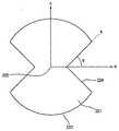
- the lens 22 includes an upper surface portion 221, a lower surface portion 222, a side surface portion 223, and a cutout portion 224 in which a portion of the side surface portion is cut in the center direction.
- the upper surface portion 221 of the lens 22 is curved at a predetermined curvature and forms an aspheric shape.
- the upper surface portion 221 of the lens 22 may be formed in a parabolic shape.
- the central portion 225 of the lens 22 forms a shape recessed from an upper side of the light emitting device 220 to a straight distance.
- a bottom center portion 226 is formed at the center of the bottom portion 222 of the lens 22, and the bottom center portion 226 is formed by spreading light emitted from the light emitting element 21. It is incident on the upper surface portion 221 serves to reduce the yellowish (yellowish) phenomenon of the lens upper surface.
- the cross section of the bottom central portion 226 may have various shapes such as semicircular, elliptical, and inclined straight. When the shape of the bottom center 226 has a curved shape that is rounded as a result of the experiment, it is possible to minimize the hot spot (light spot) where the light is concentrated at one point, and the light spreads widely, the upper surface of the lens 22 It can be confirmed that incident on 221 occurs.
- the bottom center 226 may be an air layer, and as another embodiment, a separate lens may be interposed into the bottom center 226. The separate lens may be molded in the light emitting device 21 as a resin in which phosphors are mixed.
- the upper surface portion 221 of the lens 22 functions to totally reflect the light emitted from the light emitting element 21 to the image in the lateral direction.
- the total reflection angle ⁇ c is defined by Snell's law as follows.
- the curvature of the upper surface portion 221 is preferably formed such that the incident angle of light incident on the upper surface portion 221 is 42 degrees or more. Then, most of the light incident on the upper surface portion 221 of the lens 22 is totally reflected and diffused into the light guide layer, and only a part of the light passes through the lens 22 and moves toward the display panel 15.
- the light blocking pattern layer may be formed on the upper surface of the lens 22 so that a part of the light traveling toward the display panel 15 may be reflected back to the light guide layer.
- the center portion 225 of the lens 22 may be recessed up to a straight distance from the bottom center portion 226.
- the spread of light incident on the lens 22 is determined by the depth H of the lens center portion 225 / the pitch P of the lens upper surface portion 221.
- the pitch of the upper surface of the lens means the distance from the central portion 225 of the lens 22 to the edge of the curved surface of the upper surface of the lens 22.
- the H / P value which means the spread of light incident on the lens 22, is defined as Luminous intensity distribution of the lens. As the light distribution value increases, total reflection of light increases, so that light spreads uniformly to a distance.
- the degree of light distribution is preferably 0.3 or more, and more preferably about 0.5.
- FIG. 5 is a plan view illustrating a form in which light is reflected and refracted through a lens according to an exemplary embodiment of the present invention.
- the side surface portion of the lens 22 according to the exemplary embodiment of the present invention is formed with a cutout 224 recessed in the center direction. This may be referred to as a structure in which the side portion of the conventional isotropic optical lens is cut.
- the lens 22 when the lens 22 is viewed from the top surface, a part of the light incident on the side portion of the cutout portion 224 passes through and passes in the left and right directions, and most of the remaining light is totally reflected to round the side portion.
- the + n and -n axis directions may be defined as the width direction of the display panel.
- a medium is distributed while being refracted by meeting other air and spreading in a fan shape.
- the n-axis end portion forms a side portion that is rounded to a predetermined curvature, light is spread widely by refraction while passing through the lens end portion.
- a part of the lens 22 is cut to form an anisotropic light distribution, so that the light emitted from the light emitting element 21 is concentrated in one axis (n-axis) direction instead of isotropically spreading. To spread farther. As a result, even if the number of the light emitting elements 21 is reduced for the display panel of the same size, there is an advantage that the light efficiency does not decrease.
- the cut surface of the cutout 224 is illustrated as forming a straight line in the drawing, it is not limited thereto, and the cut surface may be rounded to a predetermined curvature. Since the light spreading distance needs to be adjusted according to the size of the display panel, it can be appropriately selected in the design process. As an example, the cut surface of the cutout 224 is rounded, so that the shape of the plan view may form a peanut shape or an eight-character shape as a whole.
- the amount of light totally reflected by the cutout 224 may vary according to the inclination or curvature of the cutout forming the cutout 224.
- the formation conditions of the cutout 224 to increase the total reflectance will be described.
- FIG. 6 is a view for explaining the shape conditions of the incision to achieve the anisotropic light distribution of the lens according to the embodiment of the present invention.
- anisotropic light distribution is achieved so that the light emitted from the light emitting element 21 is not distributed isotropically distributed in the horizontal direction with respect to the vertical axis, but is concentrated in one axial direction and spread far. Incision structure of the lens to be shown.
- the incision 224 recessed to a predetermined depth is formed on the side of the lens 22 so that light does not spread in all directions but spreads substantially symmetrically in a single axis direction.
- the light incident toward the cutout 224 is reflected in the n-axis direction by total reflection as much as possible, rather than being transmitted and spread in the m-axis direction.
- the light is spread far in the single axis direction.
- the same light efficiency can be obtained by arranging the light emitting units in the horizontal direction of the backlight unit only at regular intervals in the longitudinal direction. As a result, the number of light emitting units provided in the backlight unit is reduced.
- the amount of light totally reflected from the incision plane is determined according to the inclination plane of the incision plane 224, and the incision plane is illustrated as a straight inclined plane in the drawing, but may also form a rounded curved slope have. That is, as described above, a peanut or 8-shaped lens plane structure is also possible. Under these conditions, in order to maximize the total reflection amount, the axis (m-axis) passing through the central portion 225 of the lens and the central portion of the cutout portion 226 and the angle ⁇ formed by the tangent line passing through a certain point of the cutting surface are formed.
- the portion satisfying 30 degrees to 60 degrees is preferably 50% or more of the length of the incision surface.
- the side portion 223 of the lens 22 is acute angle with the horizontal plane has been presented as an embodiment, but is not limited thereto. That is, it is revealed that the angle formed between the side surface portion 223 of the lens 22 and the horizontal plane for the light distribution distribution can be adjusted to be perpendicular or obtuse.
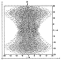
- FIG. 7 is a simulation diagram illustrating a light distribution distribution implemented by a light emitting unit assembly to which a lens structure according to an exemplary embodiment of the present invention is applied.
- the simulation is a light distribution diagram when three light emitting parts are arranged in a length direction of the display panel at intervals of 60 mm and an optical gap of a backlight unit is 20 mm.
- the optical gap means a straight line distance from the light emitting part 20 to the optical sheet 14. It can be said that the thickness of the backlight unit is substantially determined by the optical gap.
- the x axis means the length direction of the display panel
- the y axis means the width direction of the display panel. That is, in FIG. 1, the shorter side is the width direction, the longer side is the longitudinal direction, and three light emitting units 20 are arranged in the longitudinal direction.
- each light emitting part 20 diffuses in a direction parallel to the display panel, and a light distribution distance is short in a portion where an incision is formed.
- the light spreads farther out towards the other side, the rounded side.
- the luminance of the light is maintained almost uniform in the inner portion except for both edges.
- the light emitted through the side part of the lens in one light emitting part is spread to a distance corresponding to the width of the display panel.
- a blank area in which the light does not spread effectively may occur in the cutout area. Therefore, in order to minimize the blank area, the light distribution area may be partially overlapped by appropriately adjusting the distance between adjacent light emitting parts.
- the optical sheet 14 is placed in the blank area generated in the cutout area, luminance is uniformly adjusted over the entire display panel, thereby realizing surface light emission. That is, since a part of the light exiting the optical sheet 14 is reflected back and moves back toward the reflective layer 13, this blank area can be removed.
- the number of light emitting parts arranged according to the length of the display panel is determined, and the specification of the light emitting element or the spreading angle ⁇ of the cutout part is determined according to the length of the width of the display panel.
Abstract
La présente invention concerne un appareil d'affichage qui, selon un mode de réalisation, comprend : un substrat ; une unité électroluminescente, qui contient un élément électroluminescent monté sur le substrat et une lentille placée au-dessus de l'élément électroluminescent ; une couche réfléchissante, placée sur la surface supérieure du substrat ; une feuille optique, placée au-dessus de la couche réfléchissante et à une hauteur à laquelle elle est écartée de l'unité électroluminescente ; et un panneau d'affichage, placé sur la surface supérieure de la feuille optique, la lentille ayant une partie découpe formée à l'intérieur, par dépression d'une partie de sa surface latérale vers son centre, ce qui fournit une répartition anisotrope de la lumière.
Priority Applications (4)
| Application Number | Priority Date | Filing Date | Title |
|---|---|---|---|
| PCT/KR2013/001165 WO2014126278A1 (fr) | 2013-02-14 | 2013-02-14 | Appareil d'affichage |
| US14/767,829 US9829180B2 (en) | 2013-02-14 | 2013-02-14 | Display apparatus |
| EP13875208.4A EP2958097B1 (fr) | 2013-02-14 | 2013-02-14 | Appareil d'affichage |
| US15/823,111 US10151448B2 (en) | 2013-02-14 | 2017-11-27 | Display apparatus |
Applications Claiming Priority (1)
| Application Number | Priority Date | Filing Date | Title |
|---|---|---|---|
| PCT/KR2013/001165 WO2014126278A1 (fr) | 2013-02-14 | 2013-02-14 | Appareil d'affichage |
Related Child Applications (2)
| Application Number | Title | Priority Date | Filing Date |
|---|---|---|---|
| US14/767,829 A-371-Of-International US9829180B2 (en) | 2013-02-14 | 2013-02-14 | Display apparatus |
| US15/823,111 Continuation US10151448B2 (en) | 2013-02-14 | 2017-11-27 | Display apparatus |
Publications (1)
| Publication Number | Publication Date |
|---|---|
| WO2014126278A1 true WO2014126278A1 (fr) | 2014-08-21 |
Family
ID=51354271
Family Applications (1)
| Application Number | Title | Priority Date | Filing Date |
|---|---|---|---|
| PCT/KR2013/001165 WO2014126278A1 (fr) | 2013-02-14 | 2013-02-14 | Appareil d'affichage |
Country Status (3)
| Country | Link |
|---|---|
| US (2) | US9829180B2 (fr) |
| EP (1) | EP2958097B1 (fr) |
| WO (1) | WO2014126278A1 (fr) |
Families Citing this family (13)
| Publication number | Priority date | Publication date | Assignee | Title |
|---|---|---|---|---|
| EP3014327A1 (fr) * | 2013-06-27 | 2016-05-04 | Koninklijke Philips N.V. | Dispositif d'éclairage |
| KR102381328B1 (ko) * | 2015-03-30 | 2022-04-01 | 삼성디스플레이 주식회사 | 표시 장치 |
| US10222024B2 (en) * | 2015-06-03 | 2019-03-05 | Advanced Optoelectronic Technology, Inc. | Lens for light emitting device |
| US20200041096A1 (en) * | 2016-10-04 | 2020-02-06 | Signify Holding B.V. | Luminaire with spatially separated solid state lighting elements |
| JP6820778B2 (ja) * | 2017-03-21 | 2021-01-27 | 株式会社エンプラス | 光束制御部材、発光装置および面光源装置 |
| US11739928B2 (en) * | 2017-08-10 | 2023-08-29 | Archangel Device Llc | Safety light |
| JP6316494B1 (ja) * | 2017-09-26 | 2018-04-25 | 株式会社エンプラス | 面光源装置および表示装置 |
| US10802332B2 (en) * | 2017-12-26 | 2020-10-13 | Huizhou China Star Optoelectronics Technology Co., Ltd. | Low cost backlight module and display device |
| CN208041696U (zh) * | 2018-04-16 | 2018-11-02 | 京东方科技集团股份有限公司 | 背光源、背光模组和显示装置 |
| CN108535916B (zh) * | 2018-04-20 | 2020-04-28 | 武汉华星光电技术有限公司 | 直下式背光模组及其制作方法 |
| US10816850B2 (en) | 2018-04-20 | 2020-10-27 | Wuhan China Star Optoelectronics Technology Co., Ltd. | Direct-lit backlight module and manufacturing method thereof |
| KR20210101817A (ko) * | 2020-02-11 | 2021-08-19 | 현대자동차주식회사 | 자동차 램프용 확산 렌즈 및 이를 포함하는 자동차 램프 |
| CN115206201B (zh) * | 2022-07-20 | 2023-11-10 | 厦门天马微电子有限公司 | 显示面板及其制备方法、显示装置 |
Citations (5)
| Publication number | Priority date | Publication date | Assignee | Title |
|---|---|---|---|---|
| KR20060112071A (ko) * | 2005-04-26 | 2006-10-31 | 엘지전자 주식회사 | 측면 발광용 렌즈 및 그를 이용한 발광 패키지 |
| KR20070117689A (ko) * | 2005-03-29 | 2007-12-12 | 필립스 루미리즈 라이팅 캄파니 엘엘씨 | 백라이팅에 유용한 led용 와이드 방출 렌즈 |
| US20080303757A1 (en) * | 2007-06-06 | 2008-12-11 | Sony Corporation | Light emitting device, area light source apparatus and image display apparatus |
| US20110199670A1 (en) * | 2010-02-12 | 2011-08-18 | Au Optronics Corporation | Display device and light enhancement film of the display device |
| KR20120005765A (ko) * | 2010-07-09 | 2012-01-17 | 삼성전자주식회사 | 백라이트 유닛 및 이를 구비하는 디스플레이장치 |
Family Cites Families (21)
| Publication number | Priority date | Publication date | Assignee | Title |
|---|---|---|---|---|
| KR101201307B1 (ko) * | 2005-06-30 | 2012-11-14 | 엘지디스플레이 주식회사 | 백라이트유닛 |
| US6607286B2 (en) * | 2001-05-04 | 2003-08-19 | Lumileds Lighting, U.S., Llc | Lens and lens cap with sawtooth portion for light emitting diode |
| US7300185B1 (en) * | 2003-02-19 | 2007-11-27 | Opto Technology, Inc. | Quadrilateral symmetrical light source |
| KR100586970B1 (ko) * | 2004-05-28 | 2006-06-08 | 삼성전기주식회사 | 액정 디스플레이 표시장치의 백라이트 유닛 |
| KR100616598B1 (ko) * | 2004-08-11 | 2006-08-28 | 삼성전기주식회사 | 발광 다이오드 렌즈 및 이를 구비한 백라이트 모듈 |
| JP3875247B2 (ja) * | 2004-09-27 | 2007-01-31 | 株式会社エンプラス | 発光装置、面光源装置、表示装置及び光束制御部材 |
| KR101137843B1 (ko) * | 2005-06-15 | 2012-04-20 | 엘지디스플레이 주식회사 | 백라이트 유닛과 이를 이용한 액정표시장치 |
| TWI300153B (en) | 2005-12-23 | 2008-08-21 | Innolux Display Corp | Led, scanning backlight and liquid crystal display |
| DE102006050880A1 (de) * | 2006-06-30 | 2008-04-17 | Osram Opto Semiconductors Gmbh | Optoelektronisches Bauteil und Beleuchtungseinrichtung |
| JP2008108674A (ja) * | 2006-10-27 | 2008-05-08 | Stanley Electric Co Ltd | Led照明灯具 |
| JP5188077B2 (ja) | 2007-03-02 | 2013-04-24 | 株式会社光波 | 光方向変換素子及び面状発光装置 |
| KR20110025896A (ko) * | 2008-06-23 | 2011-03-14 | 파나소닉 주식회사 | 발광장치, 면 발광장치 및 표시장치 |
| CN101936502A (zh) * | 2009-06-30 | 2011-01-05 | 富准精密工业(深圳)有限公司 | 透镜、发光二极管模组及其应用的照明装置 |
| CN101963322A (zh) * | 2009-07-21 | 2011-02-02 | 富准精密工业(深圳)有限公司 | 透镜、发光二极管模组及照明装置 |
| US8602605B2 (en) * | 2010-01-07 | 2013-12-10 | Seoul Semiconductor Co., Ltd. | Aspherical LED lens and light emitting device including the same |
| US20120113621A1 (en) * | 2010-11-10 | 2012-05-10 | Taiwan Semiconductor Manufacturing Company, Ltd. | Batwing beam based led and backlight module using the same |
| CN102844609A (zh) * | 2010-12-16 | 2012-12-26 | 松下电器产业株式会社 | 背光装置和液晶显示装置以及透镜 |
| JPWO2012081187A1 (ja) * | 2010-12-16 | 2014-05-22 | パナソニック株式会社 | バックライト装置および液晶表示装置 |
| JPWO2012101715A1 (ja) * | 2011-01-25 | 2014-06-30 | パナソニック株式会社 | バックライト装置および液晶表示装置 |
| WO2012101714A1 (fr) * | 2011-01-25 | 2012-08-02 | パナソニック株式会社 | Dispositif de rétroéclairage et dispositif d'affichage à cristaux liquides |
| JP6207236B2 (ja) * | 2013-05-28 | 2017-10-04 | 三菱電機株式会社 | 点光源、面状光源装置および表示装置 |
-
2013
- 2013-02-14 US US14/767,829 patent/US9829180B2/en active Active
- 2013-02-14 WO PCT/KR2013/001165 patent/WO2014126278A1/fr active Application Filing
- 2013-02-14 EP EP13875208.4A patent/EP2958097B1/fr active Active
-
2017
- 2017-11-27 US US15/823,111 patent/US10151448B2/en active Active
Patent Citations (5)
| Publication number | Priority date | Publication date | Assignee | Title |
|---|---|---|---|---|
| KR20070117689A (ko) * | 2005-03-29 | 2007-12-12 | 필립스 루미리즈 라이팅 캄파니 엘엘씨 | 백라이팅에 유용한 led용 와이드 방출 렌즈 |
| KR20060112071A (ko) * | 2005-04-26 | 2006-10-31 | 엘지전자 주식회사 | 측면 발광용 렌즈 및 그를 이용한 발광 패키지 |
| US20080303757A1 (en) * | 2007-06-06 | 2008-12-11 | Sony Corporation | Light emitting device, area light source apparatus and image display apparatus |
| US20110199670A1 (en) * | 2010-02-12 | 2011-08-18 | Au Optronics Corporation | Display device and light enhancement film of the display device |
| KR20120005765A (ko) * | 2010-07-09 | 2012-01-17 | 삼성전자주식회사 | 백라이트 유닛 및 이를 구비하는 디스플레이장치 |
Also Published As
| Publication number | Publication date |
|---|---|
| US9829180B2 (en) | 2017-11-28 |
| US20150369454A1 (en) | 2015-12-24 |
| US20180080632A1 (en) | 2018-03-22 |
| EP2958097B1 (fr) | 2019-09-18 |
| US10151448B2 (en) | 2018-12-11 |
| EP2958097A1 (fr) | 2015-12-23 |
| EP2958097A4 (fr) | 2016-08-24 |
Similar Documents
| Publication | Publication Date | Title |
|---|---|---|
| WO2014126278A1 (fr) | Appareil d'affichage | |
| USRE48207E1 (en) | Display apparatus | |
| KR101957184B1 (ko) | 백라이트 유닛 및 그를 구비한 디스플레이 장치 | |
| WO2014014134A1 (fr) | Dispositif d'affichage | |
| WO2014098476A1 (fr) | Lentille pour diode électroluminescente du type à émission latérale, unité de rétro-éclairage et dispositif d'affichage la comportant | |
| KR100942490B1 (ko) | 전면에 광학부재를 구비하는 백라이트 유닛용 도광판 및이를 이용한 액정표시장치 | |
| EP2594972B1 (fr) | Unité de rétroéclairage et appareil d'affichage correspondant | |
| KR102080348B1 (ko) | 디스플레이 장치 | |
| KR101058298B1 (ko) | 도광판 및 백라이트부 | |
| TW201124760A (en) | Light guide plate, light guide plate manufacturing method, surface light source device, and liquid crystal display device | |
| WO2014025193A1 (fr) | Lentille pour diode électroluminescente, unité de rétroéclairage et dispositif d'affichage la comportant | |
| KR20100024752A (ko) | 프리즘 시트와 이를 구비한 액정표시장치 | |
| US8550668B2 (en) | Light control member with intersecting groups of parallel prisms, and light-emitting device using such member | |
| WO2014126279A1 (fr) | Dispositif d'affichage | |
| US10534126B2 (en) | Lighting device and display device | |
| WO2011030941A1 (fr) | Appareil de rétroéclairage à gradation locale | |
| US20140313772A1 (en) | Illumination device, and display device provided therewith | |
| JP2010192246A (ja) | 光拡散板、光学シート、バックライトユニットおよびディスプレイ装置 | |
| WO2017222155A1 (fr) | Plaque guide de lumière pour unité de rétroéclairage de type direct | |
| JP2010135219A (ja) | 面光源素子およびこれを用いた画像表示装置 | |
| KR101261620B1 (ko) | 헤테로-코닉 렌즈 형상의 단면을 갖는 렌티큘러 광학 시트 및 이를 포함하는 백라이트 유닛 | |
| KR20150098072A (ko) | 디스플레이 장치 | |
| KR20170141300A (ko) | 로컬 디밍이 가능한 도광판 및 이를 구비하는 디스플레이 장치 | |
| KR100869147B1 (ko) | 백라이트 유닛용 도광판 | |
| WO2011021737A1 (fr) | Dispositif rétroéclairé comportant une fonction de gradation locale |
Legal Events
| Date | Code | Title | Description |
|---|---|---|---|
| 121 | Ep: the epo has been informed by wipo that ep was designated in this application |
Ref document number: 13875208 Country of ref document: EP Kind code of ref document: A1 |
|
| WWE | Wipo information: entry into national phase |
Ref document number: 2013875208 Country of ref document: EP |
|
| WWE | Wipo information: entry into national phase |
Ref document number: 14767829 Country of ref document: US |
|
| NENP | Non-entry into the national phase |
Ref country code: DE |