WO2014119059A1 - 受電装置および送電装置 - Google Patents
受電装置および送電装置 Download PDFInfo
- Publication number
- WO2014119059A1 WO2014119059A1 PCT/JP2013/078380 JP2013078380W WO2014119059A1 WO 2014119059 A1 WO2014119059 A1 WO 2014119059A1 JP 2013078380 W JP2013078380 W JP 2013078380W WO 2014119059 A1 WO2014119059 A1 WO 2014119059A1
- Authority
- WO
- WIPO (PCT)
- Prior art keywords
- transformer
- voltage
- power transmission
- electrode
- power
- Prior art date
- Legal status (The legal status is an assumption and is not a legal conclusion. Google has not performed a legal analysis and makes no representation as to the accuracy of the status listed.)
- Ceased
Links
Images


Classifications
-
- H—ELECTRICITY
- H02—GENERATION; CONVERSION OR DISTRIBUTION OF ELECTRIC POWER
- H02J—ELECTRIC POWER NETWORKS; CIRCUIT ARRANGEMENTS OR SYSTEMS FOR SUPPLYING OR DISTRIBUTING ELECTRIC POWER; SYSTEMS FOR STORING ELECTRIC ENERGY
- H02J50/00—Circuit arrangements or systems for wireless supply or distribution of electric power
- H02J50/10—Circuit arrangements or systems for wireless supply or distribution of electric power using inductive coupling
- H02J50/12—Circuit arrangements or systems for wireless supply or distribution of electric power using inductive coupling of the resonant type
-
- H—ELECTRICITY
- H02—GENERATION; CONVERSION OR DISTRIBUTION OF ELECTRIC POWER
- H02J—ELECTRIC POWER NETWORKS; CIRCUIT ARRANGEMENTS OR SYSTEMS FOR SUPPLYING OR DISTRIBUTING ELECTRIC POWER; SYSTEMS FOR STORING ELECTRIC ENERGY
- H02J50/00—Circuit arrangements or systems for wireless supply or distribution of electric power
- H02J50/70—Circuit arrangements or systems for wireless supply or distribution of electric power involving the reduction of electric, magnetic or electromagnetic leakage fields
Definitions
- the present invention relates to a power receiving device, and more particularly, to a power receiving device having a function of stepping down a received AC voltage.
- the present invention also relates to a power transmission device, and more particularly, to a power transmission device having a function of boosting an AC voltage to be transmitted.
- a conventional electric field coupling type wireless power transmission system is disclosed in Patent Document 1.
- a high-frequency voltage generation circuit provided in the power transmission device generates a high-frequency voltage of, for example, 100 kHz to several tens of MHz.
- the generated high-frequency voltage is boosted by a booster circuit formed by a booster transformer and an inductor.
- the passive electrode and the active electrode of the power transmission device are field-coupled with the passive electrode and the active electrode provided in the power reception device, and the boosted high-frequency voltage is transmitted to the power reception device via these electrodes.
- the power receiving device is provided with a step-down circuit formed by a step-down transformer and an inductor.
- the high-frequency voltage transmitted by the electric field coupling is stepped down by this step-down circuit and then supplied to the secondary battery through the rectifying and smoothing circuit.
- the specifications (specifically, withstand voltage, inductance value, Q value) of the step-up transformer and the step-down transformer are strict, it is difficult to reduce the height of these transformers and thus to downsize the system module. As a result, it becomes difficult to incorporate the system into a mobile device such as a mobile phone or a smartphone that is required to be downsized.
- a transformer using windings if the step-up transformer and the step-down transformer are used for resonance, a transformer satisfying all necessary specifications (withstand voltage, Q value, size, cost, etc.) can be obtained. It is difficult to choose.
- a main object of the present invention is to provide a power receiving device that is excellent in power receiving efficiency and can be miniaturized.
- Another object of the present invention is to provide a power transmission device that is excellent in power transmission efficiency and can be miniaturized.
- the power receiving device (20: reference numerals corresponding to the embodiments; the same applies hereinafter) includes a power receiving electrode (E3, E4) to which an alternating voltage with a predetermined frequency transmitted from the power transmitting device (10) is applied, A first step-down means (24, 30, 32) for reducing the AC voltage applied to the power receiving electrode, and a second step-down means for stepping down the AC voltage stepped down by the first step-down means. 26, 30, 40), rectifying / smoothing means (28) for rectifying and smoothing current based on the AC voltage stepped down by the second step-down means, and supply means (Vout) for supplying the output of the rectifying and smoothing means to the load (22) Is provided.
- a power receiving electrode E3, E4
- a first step-down means 24, 30, 32
- a second step-down means for stepping down the AC voltage stepped down by the first step-down means. 26, 30, 40
- rectifying / smoothing means (28) for rectifying and smoothing current based on the AC voltage
- the power transmission device includes power transmission electrodes (E1, E2) to which an AC voltage is applied, and the power reception electrode corresponds to an electrode that is electric field coupled with the power transmission electrode.
- the first step-down means includes a first piezoelectric transformer (30).
- the first step-down means includes a plurality of inductors (L3, L4) connected in series with each other and a capacitor (C2) connected in parallel with a part of the plurality of inductors.
- the second lowering means includes a second piezoelectric transformer (40).
- a power transmission device (10) includes a generating means (12) for generating an alternating voltage of a predetermined frequency, a first boosting means (14) for boosting an alternating voltage generated from the generating means, and a resonance in the vicinity of the predetermined frequency.
- a second booster (16) having a characteristic and boosting the AC voltage boosted by the first booster; and a power transmission electrode (E1, E2) to which the AC voltage boosted by the second booster is applied .
- the alternating voltage transmitted from the power transmission device exhibits a predetermined frequency
- the first step-down means for stepping down the alternating voltage applied to the power receiving electrode has a characteristic of resonating in the vicinity of the predetermined frequency. Power reception efficiency can be obtained.
- the AC voltage transmitted from the power transmission device is stepped down stepwise by the first step-down device and the second step-down device. For this reason, the specification of each step-down means can be relaxed, and the height of each step-down means can be reduced.
- the output voltage of the first step-down unit may be high, the output current of the first step-down unit can be suppressed, and thereby the first step-down unit can be reduced in height.
- the power receiving device can be reduced in size.
- the AC voltage generated from the AC power source has a predetermined frequency
- the second booster that outputs the AC voltage applied to the power transmission electrode has a characteristic of resonating in the vicinity of the predetermined frequency. Transmission efficiency can be obtained.
- the AC voltage generated from the AC power source is boosted stepwise by the first booster and the second booster. For this reason, the specification of each booster can be relaxed, and the height of each booster can be reduced.
- the power receiving device can be reduced in size.
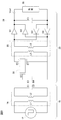
- the power transmission system of this embodiment includes a power transmission device 10 and a power reception device 20.
- the power transmission device 10 is formed by a high-frequency voltage generation circuit 12 and a step-up transformer 14, and an active electrode E1 and a passive electrode E2 for electric field coupling.
- the power receiving device 20 is formed by an active electrode E3 and a passive electrode E4 for electric field coupling, a primary step-down transformer 24, a secondary step-down transformer 26, and a rectifying / smoothing circuit 28.
- the high frequency voltage generation circuit 12 generates a high frequency voltage (AC voltage) of 200 kHz.
- One output end and the other output end of the high-frequency voltage generation circuit 12 are connected to one end and the other end of the primary coil L1 forming the step-up transformer 14, respectively.
- the secondary coil L2 forming the step-up transformer 14 has a larger number of turns than the number of turns of the primary coil L1.
- One end of the secondary coil L2 is connected to the active electrode E1, and the other end of the secondary coil L2 is connected to the passive electrode E2.
- the primary step-down transformer 24 has a coil L3 having one end connected to the active electrode E3.
- the other end of the coil L3 is connected to one end of the coil L4, and the other end of the coil L4 is connected to the passive electrode E4.
- Capacitor C2 is connected in parallel with coil L4 and forms a resonant circuit with coils L3 and L4.
- the number of turns and the winding diameter of the coil L3 are adjusted to “500” and “0.1 mm”, respectively, and the number of turns and the winding diameter of the coil L4 are adjusted to “50” and “0.2 mm”, respectively.
- the size of the coil L3 is adjusted to 15 mm ⁇ 6 mm ⁇ 5 mm (height is 5 mm)
- the size of the coil L4 is adjusted to 10 mm ⁇ 10 mm ⁇ 5 mm (height is 5 mm).
- the capacitance of the capacitor C2 is adjusted so that the resonance frequency of the resonance circuit shows a frequency in the vicinity of 200 kHz.
- the secondary step-down transformer 26 is formed by a primary coil L5 and a secondary coil L6. Both primary coil L5 and secondary coil L6 are formed in a pattern on the substrate. The number of turns and the pattern width of the primary coil L5 are adjusted to “25” and “0.5 mm”, respectively, and the number of turns and the pattern width of the secondary coil L6 are adjusted to “5” and “1.0 mm”, respectively. Further, the size of the secondary step-down transformer 26 is adjusted to 20 mm ⁇ 20 mm ⁇ 5 mm (height is 5 mm).
- the one end of the primary coil L5 is connected to one end of the coil L4, and the other end of the primary coil L5 is connected to the other end of the coil L4.
- One end of the secondary coil L6 is connected to the anode of the diode D1 and the cathode of the diode D3 that form the rectifying and smoothing circuit.
- the other end of the secondary coil L6 is connected to the anode of the diode D2 and the cathode of the diode D4 that form the rectifying and smoothing circuit 28.
- the cathodes of the diodes D1 and D2 are connected to one end of the capacitor C1, and the anodes of the diodes D3 and D4 are connected to the other end of the capacitor C1.
- a load 22 such as a secondary battery is provided in parallel with the capacitor C1.
- the high frequency voltage generated from the high frequency voltage generation circuit 12 is boosted by the step-up transformer 14 and then applied to the active electrode E1 and the passive electrode E2.
- a high-frequency voltage based on the high-frequency voltage thus applied to the active electrode E3 and the passive electrode E4 of the power receiving device 20 is excited by electric field coupling.
- the excited high frequency voltage is stepped down stepwise by the primary step-down transformer 24 and the secondary step-down transformer 26.
- the stepped-down high frequency voltage is full-wave rectified by the diodes D1 to D4, and the rectified voltage is smoothed by the capacitor C1.
- a current based on the DC voltage thus generated is supplied to the load 22 via the output terminal Vout.
- the high-frequency voltage transmitted from the power transmission device 10 exhibits a frequency of 200 kHz. Since the primary step-down transformer 24 has a characteristic of resonating in the vicinity of 200 kHz, high power receiving efficiency is obtained. Further, the high frequency voltage transmitted from the power transmission device 10 is stepped down stepwise by the primary step-down transformer 24 and the secondary step-down transformer 26. Therefore, the specifications (withstand voltage, inductance value, Q value) of the primary step-down transformer 24 and the secondary step-down transformer 26 can be relaxed, and the primary step-down transformer 24 and the secondary step-down transformer 26 can be reduced in height. It becomes.
- the output voltage of the primary step-down transformer 24 may be higher than when the voltage is stepped down by a single transformer, the output current of the primary step-down transformer 24 can be suppressed. Low profile is achieved.
- the secondary step-down transformer 26 can be reduced in height. As a result of the reduction in height of the primary step-down transformer 24 and the secondary step-down transformer 26, the power receiving device 20 can be downsized.
- the secondary step-down transformer does not need to be resonant, a transformer with strong coupling and small leakage inductance can be used, and the system can be adapted to the load specifications without significantly changing the conditions of the resonant circuit section. It is easy to select the most suitable step-down transformer.
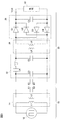
- the power transmission system of another embodiment is the same as the power transmission system shown in FIG. 1 except that the primary step-down transformer 24 of the power receiving device 20 is replaced by a single plate piezoelectric transformer 30. Therefore, the description of the overlapping parts is omitted as much as possible.
- the single-plate piezoelectric transformer 30 has a single electrode E5 on the secondary side and two electrodes E6 and E7 on the primary side.
- the secondary electrode E5 is connected to the active electrode E3, and the primary electrodes E6 and E7 form the secondary stepping transformer 26. Are connected to one end and the other end.
- the electrode E7 is also connected to the passive electrode E4.
- the resonance frequency of the single-plate piezoelectric transformer 30 is set in the vicinity of 200 kHz. Further, the size of the single-plate piezoelectric transformer 30 is adjusted to 10 mm ⁇ 25 mm ⁇ 3 mm (height is 3 mm). The single-plate piezoelectric transformer 30 that is allowed to have a height of about 3 mm can transmit power of about 10 W.
- the single plate piezoelectric transformer 30 Since it is difficult to ensure a large step-down ratio in the single plate piezoelectric transformer 30, the single plate piezoelectric transformer 30 only steps down the high-frequency voltage transmitted from the power transmission device 10 to about 1/2 to 1/5. However, the withstand voltage of the secondary step-down transformer 26 can be lowered by providing the single-plate piezoelectric transformer 30, and the secondary step-down transformer 26 can be reduced in height. Since the size of the single-plate piezoelectric transformer 30 is as described above, the power receiving device 20 can be reduced in size as in the embodiment of FIG.
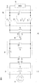
- the power transmission system according to another embodiment is similar to the power transmission system shown in FIG. 2 except that the single-plate piezoelectric transformer 30 shown in FIG. 2 is replaced by a step-down circuit 32 having an equivalent element. Since it is the same as that of a transmission system, the description about the overlapping part is omitted as much as possible.
- the step-down circuit 32 has a capacitor C3 having one end connected to the active electrode E3 and the other end connected to the passive electrode E4. One end of the capacitor C3 is connected to one end of the capacitor C4, and the other end of the capacitor C4 is connected to one end of the capacitor C5 via the coil L7. The other end of the capacitor C5 is connected to the other end of the capacitor C3.
- the primary coil L5 that forms the secondary step-down transformer 26 is connected in parallel with the capacitor C5.
- the resonant frequency of the step-down circuit 32 is adjusted to around 200 kHz by adjusting the capacitances of the capacitors C3 to C5 and the inductance of the coil L7. Further, the high-frequency voltage transmitted from the power transmission circuit 10 is stepped down by the coil L7. Also in this embodiment, miniaturization of the power receiving device 20 is realized as in the embodiment of FIG.
- the power transmission system of still another embodiment is the power transmission system shown in FIG. 1 except that the secondary step-down transformer 26 of the power receiving device 20 is replaced by the single-plate piezoelectric transformer 40 described above. Since it is the same as that of the system, description of overlapping parts is omitted as much as possible.
- the single-plate piezoelectric transformer 40 has a single electrode E5 on the secondary side and two electrodes E6 and E7 on the primary side.
- the secondary electrode E5 is connected to one end of the capacitor C2
- the primary electrode E6 is connected to the anode of the diode D1 and the cathode of the diode D3.
- the primary side electrode E7 is connected to the anode of the diode D2 and the cathode of the diode D4.
- an inductor L8 for impedance matching between the single plate piezoelectric transformer 40 and the rectifying / smoothing circuit 28 is added between the primary-side electrodes E6 and E7.
- the primary step-down transformer 24 and the single-plate piezoelectric transformer 40 can be reduced in height, and the power receiving device 20 can be reduced in size.
- the power transmission system of another embodiment is shown in FIG. 1 except that the secondary step-up transformer 16 is added to the power transmission device 10 and the primary step-down transformer 24 is omitted from the power reception device 20. Since it is the same as that of the power transmission system, description of overlapping parts is omitted as much as possible.
- the secondary step-up transformer 16 has a capacitor C6.
- One end and the other end of the capacitor C6 are connected to one end and the other end of the secondary coil L2 forming the primary step-up transformer 14, respectively.
- One end and the other end of coil L9 are connected to one end and the other end of capacitor C6, respectively.
- One end of the coil L10 is connected to one end of the coil L9, and the other end of the coil L10 is connected to the active electrode E1.
- Passive electrode E2 is connected to the other end of coil L9.
- the capacitor C6 forms a resonance circuit together with the coils L9 and L10. Further, the capacitance of the capacitor C6 is adjusted so that the resonance frequency shows a frequency in the vicinity of 200 kHz.
- one end and the other end of the primary coil L5 forming the step-down transformer 26 are connected to the active electrode E3 and the passive electrode E4.
- the high-frequency voltage output from the high-frequency voltage generation circuit 12 exhibits a frequency of 200 kHz
- the secondary step-up transformer 16 has a characteristic of resonating in the vicinity of 200 kHz, so that high power transmission efficiency is obtained.
- the high frequency voltage is stepped up stepwise by the primary step-up transformer 14 and the secondary step-up transformer 16. Therefore, the specifications of the primary step-up transformer 14 and the secondary step-up transformer 16 can be relaxed, and the height of the primary step-up transformer 14 and the secondary step-up transformer 16 can be reduced.
- the primary step-up transformer 14 does not need to have high withstand voltage performance and does not need to be a resonance type, so that the primary step-up transformer 14 can be reduced in height. Further, since the input voltage of the secondary step-up transformer 16 is high, the input current of the secondary step-up transformer 16 can be suppressed, and thereby the height of the secondary step-up transformer 16 can be reduced. As a result of the low profile of the primary step-up transformer 14 and the secondary step-up transformer 16, the power transmission device 10 can be reduced in size.
- the secondary step-up transformer does not need to be a resonance type, a transformer with a strong coupling and a small leakage inductance can be used, and without changing the conditions of the resonance circuit section greatly, according to the specifications of the power supply, It is easy to select the optimum step-up transformer for the system.
- only one transformer of the power transmission device 10 and the power reception device 20 has a two-stage configuration.
- both transformers of the power transmission device 10 and the power reception device 20 have a two-stage configuration. Also good.
Landscapes
- Engineering & Computer Science (AREA)
- Computer Networks & Wireless Communication (AREA)
- Power Engineering (AREA)
- Dc-Dc Converters (AREA)
Abstract
Description
14 …昇圧トランス
16 …二次昇圧トランス
20 …受電装置
24,32 …一次降圧トランス
26 …二次降圧トランス
28 …整流平滑回路
30 …単板圧電トランス
Claims (6)
- 送電装置から電界結合により伝送された既定周波数の交流電圧が印加される受電電極、
前記既定周波数の近傍で共振する特性を有し、前記受電電極に印加された交流電圧を降圧させる第1降圧手段、
前記第1降圧手段によって降圧された交流電圧を降圧させる第2降圧手段、
前記第2降圧手段によって降圧された交流電圧に基づく電流を整流平滑する整流平滑手段、および
前記整流平滑手段の出力が供給される負荷を備える、受電装置。 - 前記送電装置は前記交流電圧が印加される送電電極を備え、
前記受電電極は前記送電電極と電界結合される電極に相当する、請求項1記載の受電装置。 - 前記第1降圧手段は第1圧電トランスを含む、請求項1または2記載の受電装置。
- 前記第1降圧手段は、互いに直列接続された複数のインダクタ、および前記複数のインダクタの一部と並列接続されたキャパシタを含む、請求項1または2記載の受電装置。
- 前記第2降圧手段は第2圧電トランスを含む、請求項1ないし4のいずれかに記載の受電装置。
- 既定周波数の交流電圧を発生する発生手段、
前記発生手段から発生された交流電圧を昇圧させる第1昇圧手段、
前記既定周波数の近傍で共振する特性を有し、前記第1昇圧手段によって昇圧された交流電圧を昇圧させる第2昇圧手段、および
前記第2昇圧手段によって昇圧された交流電圧が印加される送電電極を備える、送電装置。
Priority Applications (2)
| Application Number | Priority Date | Filing Date | Title |
|---|---|---|---|
| JP2014559493A JPWO2014119059A1 (ja) | 2013-01-29 | 2013-10-18 | 受電装置および送電装置 |
| CN201390000686.3U CN204497855U (zh) | 2013-01-29 | 2013-10-18 | 受电装置以及送电装置 |
Applications Claiming Priority (2)
| Application Number | Priority Date | Filing Date | Title |
|---|---|---|---|
| JP2013-014878 | 2013-01-29 | ||
| JP2013014878 | 2013-01-29 |
Publications (1)
| Publication Number | Publication Date |
|---|---|
| WO2014119059A1 true WO2014119059A1 (ja) | 2014-08-07 |
Family
ID=51261795
Family Applications (1)
| Application Number | Title | Priority Date | Filing Date |
|---|---|---|---|
| PCT/JP2013/078380 Ceased WO2014119059A1 (ja) | 2013-01-29 | 2013-10-18 | 受電装置および送電装置 |
Country Status (3)
| Country | Link |
|---|---|
| JP (1) | JPWO2014119059A1 (ja) |
| CN (1) | CN204497855U (ja) |
| WO (1) | WO2014119059A1 (ja) |
Citations (4)
| Publication number | Priority date | Publication date | Assignee | Title |
|---|---|---|---|---|
| JPH0934571A (ja) * | 1995-07-24 | 1997-02-07 | Toyo Electric Mfg Co Ltd | 静止型電力変換装置 |
| JP2000270543A (ja) * | 1999-03-19 | 2000-09-29 | Toko Inc | 圧電トランスを用いたインバータ回路 |
| JP2007028812A (ja) * | 2005-07-19 | 2007-02-01 | Nissan Motor Co Ltd | 電源装置 |
| US20120286583A1 (en) * | 2011-05-13 | 2012-11-15 | Murata Manufacturing Co., Ltd | Power Transmitting Device, Power Receiving Device, and Power Transmission System |
-
2013
- 2013-10-18 JP JP2014559493A patent/JPWO2014119059A1/ja active Pending
- 2013-10-18 CN CN201390000686.3U patent/CN204497855U/zh not_active Expired - Lifetime
- 2013-10-18 WO PCT/JP2013/078380 patent/WO2014119059A1/ja not_active Ceased
Patent Citations (4)
| Publication number | Priority date | Publication date | Assignee | Title |
|---|---|---|---|---|
| JPH0934571A (ja) * | 1995-07-24 | 1997-02-07 | Toyo Electric Mfg Co Ltd | 静止型電力変換装置 |
| JP2000270543A (ja) * | 1999-03-19 | 2000-09-29 | Toko Inc | 圧電トランスを用いたインバータ回路 |
| JP2007028812A (ja) * | 2005-07-19 | 2007-02-01 | Nissan Motor Co Ltd | 電源装置 |
| US20120286583A1 (en) * | 2011-05-13 | 2012-11-15 | Murata Manufacturing Co., Ltd | Power Transmitting Device, Power Receiving Device, and Power Transmission System |
Also Published As
| Publication number | Publication date |
|---|---|
| CN204497855U (zh) | 2015-07-22 |
| JPWO2014119059A1 (ja) | 2017-01-26 |
Similar Documents
| Publication | Publication Date | Title |
|---|---|---|
| JP5804073B2 (ja) | スイッチング電源装置 | |
| TWI407677B (zh) | Power conversion device | |
| JP5550785B2 (ja) | 非接触型の誘導電力伝送システムの回路 | |
| JP5817835B2 (ja) | スイッチング電源装置 | |
| US20120049993A1 (en) | Transformer integrated with inductor | |
| WO2013146017A1 (ja) | 電力伝送システム及びそれに用いる送電装置 | |
| CN104981964B (zh) | 无线电力传输设备及其方法 | |
| JP2010104159A (ja) | 受電端末、および無接点電力伝送システム | |
| WO2020195654A1 (ja) | 非接触給電装置 | |
| JP6188820B2 (ja) | 高周波電源用整流回路 | |
| CN107346918A (zh) | 一种无线电能传输装置 | |
| TWI863918B (zh) | 用於傳輸電力至具轉換器之電力負載之裝置 | |
| JP6188824B2 (ja) | 高周波電源用整流回路 | |
| WO2022004034A1 (ja) | ワイヤレス給電システム | |
| JP6180548B2 (ja) | 高周波電源用整流回路 | |
| JP6183243B2 (ja) | 電力伝送システム、受電装置及び送電装置 | |
| WO2020189351A1 (ja) | 非接触給電装置 | |
| KR101394018B1 (ko) | 전력 공급 장치 및 무선전력 송신장치 | |
| WO2014119059A1 (ja) | 受電装置および送電装置 | |
| US9991749B2 (en) | Coil unit, wireless power feeding device, wireless power receiving device, and wireless power transmission device | |
| JP2020018060A (ja) | 受電装置及び無線給電システム | |
| US8564988B2 (en) | DC-DC converter | |
| JP6188825B2 (ja) | 高周波電源用整流回路 | |
| JPWO2009025129A1 (ja) | 直流低電圧電源装置 | |
| WO2024262209A1 (ja) | 非接触給電装置及び受電装置 |
Legal Events
| Date | Code | Title | Description |
|---|---|---|---|
| WWE | Wipo information: entry into national phase |
Ref document number: 201390000686.3 Country of ref document: CN |
|
| 121 | Ep: the epo has been informed by wipo that ep was designated in this application |
Ref document number: 13874072 Country of ref document: EP Kind code of ref document: A1 |
|
| ENP | Entry into the national phase |
Ref document number: 2014559493 Country of ref document: JP Kind code of ref document: A |
|
| NENP | Non-entry into the national phase |
Ref country code: DE |
|
| 122 | Ep: pct application non-entry in european phase |
Ref document number: 13874072 Country of ref document: EP Kind code of ref document: A1 |