WO2014115441A1 - 液晶表示装置 - Google Patents
液晶表示装置 Download PDFInfo
- Publication number
- WO2014115441A1 WO2014115441A1 PCT/JP2013/083449 JP2013083449W WO2014115441A1 WO 2014115441 A1 WO2014115441 A1 WO 2014115441A1 JP 2013083449 W JP2013083449 W JP 2013083449W WO 2014115441 A1 WO2014115441 A1 WO 2014115441A1
- Authority
- WO
- WIPO (PCT)
- Prior art keywords
- liquid crystal
- field
- signal lines
- crystal panel
- light
- Prior art date
- Legal status (The legal status is an assumption and is not a legal conclusion. Google has not performed a legal analysis and makes no representation as to the accuracy of the status listed.)
- Ceased
Links
Images


























Classifications
-
- G—PHYSICS
- G09—EDUCATION; CRYPTOGRAPHY; DISPLAY; ADVERTISING; SEALS
- G09G—ARRANGEMENTS OR CIRCUITS FOR CONTROL OF INDICATING DEVICES USING STATIC MEANS TO PRESENT VARIABLE INFORMATION
- G09G3/00—Control arrangements or circuits, of interest only in connection with visual indicators other than cathode-ray tubes
- G09G3/20—Control arrangements or circuits, of interest only in connection with visual indicators other than cathode-ray tubes for presentation of an assembly of a number of characters, e.g. a page, by composing the assembly by combination of individual elements arranged in a matrix no fixed position being assigned to or needed to be assigned to the individual characters or partial characters
- G09G3/34—Control arrangements or circuits, of interest only in connection with visual indicators other than cathode-ray tubes for presentation of an assembly of a number of characters, e.g. a page, by composing the assembly by combination of individual elements arranged in a matrix no fixed position being assigned to or needed to be assigned to the individual characters or partial characters by control of light from an independent source
- G09G3/36—Control arrangements or circuits, of interest only in connection with visual indicators other than cathode-ray tubes for presentation of an assembly of a number of characters, e.g. a page, by composing the assembly by combination of individual elements arranged in a matrix no fixed position being assigned to or needed to be assigned to the individual characters or partial characters by control of light from an independent source using liquid crystals
- G09G3/3611—Control of matrices with row and column drivers
- G09G3/3674—Details of drivers for scan electrodes
- G09G3/3677—Details of drivers for scan electrodes suitable for active matrices only
-
- G—PHYSICS
- G09—EDUCATION; CRYPTOGRAPHY; DISPLAY; ADVERTISING; SEALS
- G09G—ARRANGEMENTS OR CIRCUITS FOR CONTROL OF INDICATING DEVICES USING STATIC MEANS TO PRESENT VARIABLE INFORMATION
- G09G3/00—Control arrangements or circuits, of interest only in connection with visual indicators other than cathode-ray tubes
- G09G3/20—Control arrangements or circuits, of interest only in connection with visual indicators other than cathode-ray tubes for presentation of an assembly of a number of characters, e.g. a page, by composing the assembly by combination of individual elements arranged in a matrix no fixed position being assigned to or needed to be assigned to the individual characters or partial characters
- G09G3/34—Control arrangements or circuits, of interest only in connection with visual indicators other than cathode-ray tubes for presentation of an assembly of a number of characters, e.g. a page, by composing the assembly by combination of individual elements arranged in a matrix no fixed position being assigned to or needed to be assigned to the individual characters or partial characters by control of light from an independent source
- G09G3/36—Control arrangements or circuits, of interest only in connection with visual indicators other than cathode-ray tubes for presentation of an assembly of a number of characters, e.g. a page, by composing the assembly by combination of individual elements arranged in a matrix no fixed position being assigned to or needed to be assigned to the individual characters or partial characters by control of light from an independent source using liquid crystals
- G09G3/3611—Control of matrices with row and column drivers
- G09G3/3648—Control of matrices with row and column drivers using an active matrix
-
- G—PHYSICS
- G09—EDUCATION; CRYPTOGRAPHY; DISPLAY; ADVERTISING; SEALS
- G09G—ARRANGEMENTS OR CIRCUITS FOR CONTROL OF INDICATING DEVICES USING STATIC MEANS TO PRESENT VARIABLE INFORMATION
- G09G2310/00—Command of the display device
- G09G2310/02—Addressing, scanning or driving the display screen or processing steps related thereto
- G09G2310/0202—Addressing of scan or signal lines
- G09G2310/0205—Simultaneous scanning of several lines in flat panels
-
- G—PHYSICS
- G09—EDUCATION; CRYPTOGRAPHY; DISPLAY; ADVERTISING; SEALS
- G09G—ARRANGEMENTS OR CIRCUITS FOR CONTROL OF INDICATING DEVICES USING STATIC MEANS TO PRESENT VARIABLE INFORMATION
- G09G2310/00—Command of the display device
- G09G2310/02—Addressing, scanning or driving the display screen or processing steps related thereto
- G09G2310/0235—Field-sequential colour display
-
- G—PHYSICS
- G09—EDUCATION; CRYPTOGRAPHY; DISPLAY; ADVERTISING; SEALS
- G09G—ARRANGEMENTS OR CIRCUITS FOR CONTROL OF INDICATING DEVICES USING STATIC MEANS TO PRESENT VARIABLE INFORMATION
- G09G2310/00—Command of the display device
- G09G2310/06—Details of flat display driving waveforms
- G09G2310/061—Details of flat display driving waveforms for resetting or blanking
- G09G2310/063—Waveforms for resetting the whole screen at once
-
- G—PHYSICS
- G09—EDUCATION; CRYPTOGRAPHY; DISPLAY; ADVERTISING; SEALS
- G09G—ARRANGEMENTS OR CIRCUITS FOR CONTROL OF INDICATING DEVICES USING STATIC MEANS TO PRESENT VARIABLE INFORMATION
- G09G3/00—Control arrangements or circuits, of interest only in connection with visual indicators other than cathode-ray tubes
- G09G3/20—Control arrangements or circuits, of interest only in connection with visual indicators other than cathode-ray tubes for presentation of an assembly of a number of characters, e.g. a page, by composing the assembly by combination of individual elements arranged in a matrix no fixed position being assigned to or needed to be assigned to the individual characters or partial characters
- G09G3/34—Control arrangements or circuits, of interest only in connection with visual indicators other than cathode-ray tubes for presentation of an assembly of a number of characters, e.g. a page, by composing the assembly by combination of individual elements arranged in a matrix no fixed position being assigned to or needed to be assigned to the individual characters or partial characters by control of light from an independent source
- G09G3/3406—Control of illumination source
Definitions
- the present invention relates to a liquid crystal display device, and more particularly to a liquid crystal display device that can see the other side of the screen.
- one pixel transmits a red pixel provided with a color filter that transmits red light, a green pixel provided with a color filter that transmits green light, and blue light. It is divided into three sub-pixels of a blue pixel provided with a color filter. Although color display is possible by the color filters provided in these three sub-pixels, about 2/3 of the backlight light irradiated to the liquid crystal panel is absorbed by the color filter. For this reason, the color filter type liquid crystal display device has a problem of low light utilization efficiency. Therefore, a liquid crystal display device that employs field sequential driving for performing color display without using a color filter has attracted attention.
- a display period (one frame period) of one screen is divided into three fields (first to third fields).
- a field is also called a subframe, but in the following description, the term “field” is used in a unified manner.
- the first field displays a red screen based on the red component of the input signal
- the second field displays a green screen based on the green component of the input signal
- the third field displays the input signal.
- a blue screen is displayed based on the blue component.
- a plurality of gate bus lines (scanning signal lines) provided in a liquid crystal panel are sequentially driven one by one. For this reason, for the pixels at the top of the panel, video data is written (charged) to the pixel capacity near the start of each field, and for the pixels at the center of the panel, video data is written (charged) to the pixel capacity. This is performed in the middle of the field, and for the pixels at the bottom of the panel, writing (charging) of video data to the pixel capacity is performed near the end of each field. Therefore, when the field sequential drive is adopted, it is necessary to emit the backlight in synchronization with the sequential scanning from the upper part of the panel to the lower part of the panel. In the following, the process of sequentially emitting the backlight from the upper part of the panel to the lower part of the panel is referred to as “backlight scanning”.
- the color mixture means that light of different colors are unnecessarily mixed.
- first method A conventional method in the case of performing field sequential driving using an edge light type backlight that cannot perform backlight scanning will be described. It is assumed that an LED (light emitting diode) is adopted as the backlight light source.
- the first method as shown in FIG. 26, in one frame period, a first field for displaying a red screen, a second field for displaying a green screen, and a blue screen are displayed. And the third field.
- the high portion of each waveform represents the “light emission state”
- the low portion of each waveform represents the “light off state” (this is illustrated in FIGS. 1, 8 to 12, 16, 16, and FIG. 19, the same applies to FIGS. 24 to 26 and 41).
- the red LED In the first field, the red LED (R-LED) is in a light emitting state (lighted state) throughout one field period.
- the green LED In the second field, the green LED (G-LED) is in a light emitting state throughout one field period.
- a blue LED B-LED is in a light emitting state throughout one field period.
- the display image at each time point (see FIG. 26) in one frame period is as follows.
- the display images at time point t81, time point t82, and time point t83 are images as shown in FIGS. 31, 32, and 33, respectively.
- the display images at time t84, time t85, and time t86 are images as shown in FIGS. 34, 35, and 36, respectively.
- the display images at time t87, time t88, and time t89 are images as shown in FIGS. 37, 38, and 39, respectively.
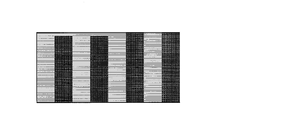
- an image visually recognized by human eyes is an image in which color mixing occurs as shown in FIG.
- the method of causing the backlight light source to emit light only in the second half period of each field by finishing the writing of the video data in each field in the first half period (hereinafter referred to as “No. 2 ”) (see FIG. 41).
- the second method it is suppressed that the state of the previous field in each field is visually recognized by human eyes. That is, the occurrence of color mixing is suppressed.
- Japanese Unexamined Patent Publication No. 2012-109227 discloses an invention of a display device that performs backlight scanning using a direct type backlight.
- Japanese Laid-Open Patent Publication No. 2012-27452 discloses an invention of a liquid crystal display device that employs a method (second method described above) that causes a backlight source to emit light only in the latter half of each field.
- the area in the panel is logically divided into three areas, and video data is written in the three areas simultaneously in parallel, thereby reducing the video data writing period in each field. Shorter than that.
- a display image at each time point (see FIG. 41) in one frame period is as follows, for example.
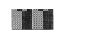
- the display images at time t91 and time t92 are images as shown in FIGS. 42 and 43, respectively.
- the display images at time t93 and time t94 are images as shown in FIGS. 42 and 44, respectively.
- the display images at time t95 and time t96 are images as shown in FIGS. 42 and 45, respectively.
- an image visually recognized by human eyes is an image in which color mixing occurs at the lower part of the panel as shown in FIG.
- Japanese Unexamined Patent Publication No. 2012-27452 it is necessary to increase the number of source bus lines in accordance with the number of divided areas in the panel. There is concern about a decrease in the rate.
- the present invention is a liquid crystal display device capable of displaying an image while the background is in a transmissive state, and adopting a configuration in which an edge light type backlight is provided on one side of the panel, and field sequential driving without causing color mixing.
- the purpose is to do.
- a first aspect of the present invention is provided in correspondence with a plurality of video signal lines, a plurality of scanning signal lines, and intersections of the plurality of video signal lines and the plurality of scanning signal lines.
- a liquid crystal panel capable of displaying an image while making a background transparent on a display unit including a plurality of pixel formation units forming a pixel matrix, and writing to a plurality of pixel capacitors included in the plurality of pixel formation units
- a liquid crystal panel driving unit that drives the plurality of video signal lines and the plurality of scanning signal lines, a backlight provided on the back side of the liquid crystal panel, and a backlight driving unit that drives the backlight
- a liquid crystal display device that displays a color image by dividing a frame period into a plurality of fields and displaying a screen of a different color for each field,
- the backlight is A plurality of light sources including a light source of K color (K is an integer of 3 or more) provided near one side of the liquid crystal panel in a direction in which
- the backlight driving unit includes the first included in the first half of each field from the start time of each field.
- the first time point is such that the length of the period from the third time point at which writing of black display data starts in each field to the first time point in the next field is longer than the liquid crystal response time. And the third time point is set.
- the light guide plate causes each color light source to emit light.
- the light intensity applied to the liquid crystal panel is gradually increased as the second side portion approaches the first side portion.
- the liquid crystal panel drive unit is configured to sequentially write video data to the plurality of pixel capacitors from the second side toward the first side, and to the plurality of pixel capacitors.
- the plurality of video signal lines and the plurality of scanning signal lines are driven so that display data is written in all rows of the pixel matrix at the same timing.
- N video signal lines (N is an integer of 2 or more) are provided for each column of the pixel matrix
- the liquid crystal panel driving unit is configured to sequentially write video data to the plurality of pixel capacitors for each N rows, and to write black display data to the plurality of pixel capacitors in the pixel matrix.
- the plurality of video signal lines and the plurality of scanning signal lines are driven so as to be performed at the same timing in all rows.
- the light guide plate causes each color light source to emit light.
- the light intensity applied to the liquid crystal panel is gradually increased as the second side portion approaches the first side portion.
- the writing of video data to the plurality of pixel capacitors is sequentially performed from the second side portion toward the first side portion.
- the light guide plate is configured so that the intensity of light given to the liquid crystal panel is uniform throughout the display unit
- the liquid crystal panel driving unit is configured to sequentially write video data to the plurality of pixel capacitors, and to write black display data to the plurality of pixel capacitors.
- the plurality of video signal lines and the plurality of scanning signal lines are driven so as to be sequentially performed in the same order as the writing of the video data.
- each field constituting one frame period video data is written into all the pixel capacities only in the first half period, and in all of the latter half period, all the video data is written.
- Data for black display is written to the pixel capacitor.
- the light source enters a light emitting state. Therefore, each field is not affected by the display of the previous field, and color mixing is prevented.
- the light source is provided on one side of the liquid crystal panel.
- the transmittance decreases as the distance from the second side of the liquid crystal panel (the side where writing is performed first) approaches the first side (the side where writing is performed last).
- the light guide plate is configured so that the intensity of light given to the liquid crystal panel gradually increases from the second side portion toward the first side portion.
- the video data is written to the pixel capacitor in a plurality of rows. For this reason, it becomes possible to lengthen the writing period to each pixel capacitor, and the deterioration of display quality due to insufficient charging is prevented.
- the black display data is sequentially written to the pixel capacitor in the same order as the video data is written to the pixel capacitor. For this reason, the transmittance does not differ between the upper part of the panel and the lower part of the panel. Therefore, the deterioration of display quality is suppressed, and the same effect as the first aspect of the present invention can be obtained without complicating the configuration of the light guide plate.
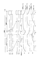
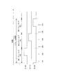
- FIG. 3 is a timing chart for explaining a driving method of the liquid crystal display device according to the first embodiment of the present invention.
- FIG. 3 is a block diagram which shows the whole function structure of a liquid crystal display device.
- FIG. 3 is a schematic diagram illustrating a configuration example of a gate driver in the first embodiment.
- It is a schematic perspective view of the liquid crystal display device in the said 1st Embodiment.
- it is a figure for demonstrating arrangement
- it is a side view of the liquid crystal display device for demonstrating the detailed structure of a backlight.
- the said 1st Embodiment it is a figure for demonstrating the optical output from the light-guide plate to the liquid crystal panel side. It is a figure which shows the structure of 1 frame period in the said 1st Embodiment. It is a figure which shows the specific structural example of 1 field period in the said 1st Embodiment. 6 is a timing chart for explaining a relationship between a black writing period and a backlight emission period in the first embodiment. It is a figure which shows the structure of 1 frame period in the 1st modification of the said 1st Embodiment. It is a figure which shows the structure of 1 frame period in the 2nd modification of the said 1st Embodiment.
- FIG. 28 is a diagram showing a target display image in a first field when the target image is the image shown in FIG. 27 in the conventional example (first method).
- FIG. 28 is a diagram showing a target display image in a second field when the target image is the image shown in FIG. 27 in the conventional example (first method).
- FIG. 28 is a diagram showing a target display image in a third field when the target image is the image shown in FIG. 27 in the conventional example (first method).
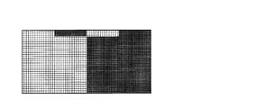
- FIG. 28 is a diagram showing a display image at a time point t81 (see FIG. 26) in a conventional example (first method).
- FIG. 27 is a diagram showing a display image at a time point t82 (see FIG.
- FIG. 27 is a diagram showing a display image at a time point t83 (see FIG. 26) in the conventional example (first method).
- FIG. 28 is a diagram showing a display image at a time point t84 (see FIG. 26) in the conventional example (first method).
- FIG. 27 is a diagram showing a display image at a time point t85 (see FIG. 26) in the conventional example (first method).
- FIG. 27 is a diagram showing a display image at a time point t86 (see FIG. 26) in the conventional example (first method).
- FIG. 28 is a diagram showing a display image at a time point t87 (see FIG. 26) in the conventional example (first method).
- FIG. 28 is a diagram showing a display image at a time point t88 (see FIG. 26) in the conventional example (first method).
- FIG. 27 is a diagram showing a display image at a time point t89 (see FIG. 26) in the conventional example (first method). It is a figure which shows the image visually recognized by a human eye in a prior art example (1st method). It is a figure which shows the structure of 1 frame period in a prior art example (2nd method). It is a figure which shows the display image in the time t91, the time t93, and the time t95 (refer FIG. 41) in a prior art example (2nd method).
- FIG. 44 is a diagram showing a display image at a time point t92 (see FIG.
- FIG. 44 is a diagram showing a display image at a time point t94 (see FIG. 41) in the conventional example (second method).
- FIG. 44 is a diagram showing a display image at a time point t96 (see FIG. 41) in the conventional example (second method). It is a figure which shows the image visually recognized by a human eye in a prior art example (2nd method).
- FIG. 2 is a block diagram showing an overall functional configuration of the liquid crystal display device according to the first embodiment of the present invention.
- the liquid crystal display device includes a frame rate conversion unit 100, a signal processing circuit 200, a source driver 300, a gate driver 400, an LED driver 500, a display unit 600, and a backlight 700.
- An LED (light emitting diode) is used as the light source for the backlight 700.
- a liquid crystal panel driving unit is realized by the source driver 300 and the gate driver 400, and a backlight driving unit is realized by the LED driver 500. It is assumed that the liquid crystal display device according to the present embodiment can operate at a driving frequency of 360 Hz.
- the display unit 600 includes a plurality (n) of source bus lines (video signal lines) SL1 to SLn and a plurality (m) of gate bus lines (scanning signal lines) GL1 to GLm. It is installed.
- a pixel forming portion 6 for forming pixels is provided corresponding to each intersection of the source bus lines SL1 to SLn and the gate bus lines GL1 to GLm.
- the display unit 600 includes a plurality (n ⁇ m) of pixel forming units 6.
- the plurality of pixel forming portions 6 are arranged in a matrix to form a pixel matrix of m rows ⁇ n columns.
- Each pixel forming portion 6 includes a TFT 60 which is a switching element having a gate terminal connected to a gate bus line GL passing through a corresponding intersection and a source terminal connected to a source bus line SL passing through the intersection.
- the pixel electrode 61 connected to the drain terminal of the TFT 60, the common electrode 64 and the auxiliary capacitance electrode 65 provided in common to the plurality of pixel forming portions 6, and the pixel electrode 61 and the common electrode 64 are formed.
- a liquid crystal capacitor 62 and an auxiliary capacitor 63 formed by the pixel electrode 61 and the auxiliary capacitor electrode 65 are included.
- the liquid crystal capacitor 62 and the auxiliary capacitor 63 constitute a pixel capacitor 66.
- the TFT 60 for example, an oxide TFT (a thin film transistor using an oxide semiconductor for a channel layer) can be employed. More specifically, InGaZnOx (indium gallium zinc oxide) (hereinafter referred to as “IGZO”), which is an oxide semiconductor mainly containing indium (In), gallium (Ga), zinc (Zn), and oxygen (O).
- IGZO-TFT in which a channel layer is formed by “IGZO” is a registered trademark
- the writing speed can be increased as compared with the conventional case.
- a transistor using an oxide semiconductor other than IGZO for the channel layer can also be employed.
- at least one of indium, gallium, zinc, copper (Cu), silicon (Si), tin (Sn), aluminum (Al), calcium (Ca), germanium (Ge), and lead (Pb) is included. The same effect can be obtained when a transistor using an oxide semiconductor for a channel layer is employed.
- the frame rate conversion unit 100 converts the frame rate of the input image signal DIN given from the outside.
- a 60 Hz input image signal DIN is given to the frame rate conversion unit 100, and 360 Hz video data is output from the frame rate conversion unit 100 as target image data DAT.
- video data is written only in the first half period (a period of one-half the length of one field) in each field constituting one frame period. That is, the drive frequency of the liquid crystal panel is 360 Hz, but the number of fields that appear in one second is 180.
- a specific method for converting the frame rate is not particularly limited.
- the signal processing circuit 200 receives the target image data DAT sent from the frame rate conversion unit 100, receives the digital video signal DV, the source start pulse signal SSP for controlling the operation of the source driver 300, the source clock signal SCK, and the latch A strobe signal LS, a gate start pulse signal GSP for controlling the operation of the gate driver 400, a gate clock signal GCK, and a black write control signal GBL, and an LED driver control signal S1 for controlling the operation of the LED driver 500; Is output.
- the source driver 300 receives the digital video signal DV, the source start pulse signal SSP, the source clock signal SCK, and the latch strobe signal LS sent from the signal processing circuit 200, and applies a driving video signal to each source bus line SL. At this time, the source driver 300 sequentially holds the digital video signal DV indicating the voltage to be applied to each source bus line SL at the timing when the pulse of the source clock signal SCK is generated. The held digital video signal DV is converted into an analog voltage at the timing when the pulse of the latch strobe signal LS is generated. The converted analog voltage is applied simultaneously to all the source bus lines SL1 to SLn as drive video signals.
- the gate driver 400 Based on the gate start pulse signal GSP and the gate clock signal GCK sent from the signal processing circuit 200, the gate driver 400 sequentially performs active scanning on the m gate bus lines GL1 to GLm during the first half of each field. Apply a signal.
- the gate driver 400 also applies to the m gate bus lines GL1 to GLm during a part of the latter half of each field (details will be described later) based on the black write control signal GBL sent from the signal processing circuit 200. Apply active scanning signals all at once.
- writing black display data separately from the original video data to the pixel capacity is referred to as “black writing”.
- a voltage corresponding to black display is called “black voltage”.
- the LED driver 500 outputs a light source control signal S2 for controlling the state of each LED constituting the backlight 700 based on the LED driver control signal S1 sent from the signal processing circuit 200.
- a light source control signal S2 for controlling the state of each LED constituting the backlight 700 based on the LED driver control signal S1 sent from the signal processing circuit 200.
- switching of the state of each LED is appropriately performed based on the light source control signal S2.
- the driving video signal is applied to the source bus lines SL1 to SLn, the scanning signal is applied to the gate bus lines GL1 to GLm, and the state of each LED is appropriately switched, whereby the input image signal DIN is changed.
- a base image is displayed on the display unit 600.
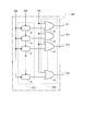
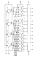
- FIG. 3 is a schematic diagram illustrating a configuration example of the gate driver 400 in the present embodiment.
- the gate driver 400 includes a shift register 410 including m flip-flop circuits 41 and a black writing control unit 420 for controlling black writing.
- the black writing control unit 420 is provided with m OR circuits 42 so as to correspond one-to-one with the flip-flop circuits 41 in the shift register 410.
- the output signal from the flip-flop circuit 41 and the black writing control signal GBL are input to the OR circuit 42.
- the output signal from the OR circuit 42 is given to the gate bus line GL as a scanning signal.
- the shift register 410 is configured such that the gate start pulse signal GSP is supplied to the first flip-flop circuit 41 and the gate clock signal GCK is supplied to all the flip-flop circuits 41 in common.
- a pulse of the gate start pulse signal GSP is given to the first-stage flip-flop circuit 41 of the shift register 410.
- the pulses included in the gate start pulse signal GSP are sequentially transferred from the first-stage flip-flop circuit 41 to the m-th stage flip-flop circuit 41.
- the output signals from the 1st to m-th stage flip-flop circuits 41 sequentially become high level.
- active scanning signals are sequentially applied to the m gate bus lines GL1 to GLm.
- the black write control signal GBL is set to the high level during a part of the second half of each field. As a result, active scanning signals are applied simultaneously to the m gate bus lines GL1 to GLm.
- FIG. 4 is a schematic perspective view of the liquid crystal display device according to the present embodiment.
- This liquid crystal display device includes a liquid crystal panel 800 including a display unit 600 for displaying an image, and a backlight 700 for irradiating light from the back surface of the liquid crystal panel 800 (to the liquid crystal panel 800).
- components for driving the liquid crystal panel 800 and the backlight 700 for example, a driver IC and a printed board on which the driver IC is mounted) are not shown.
- the backlight 700 includes an LED 71 as a light source, and a light guide plate 72 for guiding light emitted from the LED 71 to the liquid crystal panel 800.
- the backlight 700 in the present embodiment is an edge light type backlight.
- LEDs are provided in the vicinity of one side of the liquid crystal panel and in the vicinity of the other side (the left and right sides of the liquid crystal panel) in the direction in which the gate bus line extends. (See FIG. 5).
- LEDs are provided only in the vicinity of one side of the liquid crystal panel (the lower side of the liquid crystal panel) in the direction in which the source bus line extends (see FIG. 5). ).
- the reason why the LEDs are provided in this way is that the frame 81 is provided only on the lower side of the liquid crystal panel 800 in the liquid crystal display device according to the present embodiment.
- FIG. 6 is a side view of the liquid crystal display device for explaining the detailed configuration of the backlight 700 in the present embodiment.
- the LED 71 is configured by three color LEDs including a red LED 71 (R), a green LED 71 (G), and a blue LED 71 (B).
- the light guide plate 72 includes light diffusion particles (light diffusion beads) 73 for diffusing light emitted from the LEDs 71.
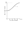
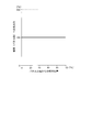
- a plurality of light diffusing particles 73 having different refractive indexes are provided in the light guide plate 72 so that the light output from the light guide plate 72 to the liquid crystal panel 800 side becomes a curve indicated by reference numeral 77 in the graph shown in FIG. Is provided.
- FIG. 1 is a side view of the liquid crystal display device for explaining the detailed configuration of the backlight 700 in the present embodiment.
- the LED 71 is configured by three color LEDs including a red LED 71 (R), a green LED 71 (G), and a blue LED 71 (B).
- the light guide plate 72 includes light
- the vertical axis represents the intensity of light output from the light guide plate 72 to the liquid crystal panel 800 (brightness appearing on the liquid crystal panel 800), and the horizontal axis represents the relative position from the upper end of the liquid crystal panel 800. (The lower end of the liquid crystal panel 800 is 100%).
- the light guide plate 72 is configured so that the intensity of light given to the liquid crystal panel 800 gradually increases as it approaches the lower end from the upper end of the liquid crystal panel 800 when each color LED 71 is in a light emitting state. Yes.
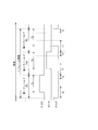
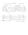
- FIG. 1 is a timing chart for explaining a driving method in the present embodiment.
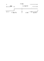
- FIG. 8 is a diagram illustrating a configuration of one frame period in the present embodiment.
- FIG. 9 is a diagram illustrating a specific configuration example of one field period in the present embodiment.
- FIG. 10 is a timing chart for explaining the relationship between the black writing period and the backlight emission period in the present embodiment.
- one frame period is composed of three fields (first to third fields).
- one frame period is 16.7 milliseconds, and one field period is about 5.56 milliseconds.
- the first field is a field in which video data for red screen is written (charged) and a red screen is displayed.
- the second field is a field in which video data for a green screen is written and a green screen is displayed.
- the third field is a field in which video data for a blue screen is written and a blue screen is displayed.
- the first to third fields are repeated. Thereby, a red screen, a green screen, and a blue screen are repeatedly displayed, and a desired color display is performed.
- the order of the first field to the third field is not particularly limited. For example, the display may be performed in the order of “blue screen, green screen, red screen”.
- video data is written to all the pixel capacitors 66 in the display unit 600 during a period T1 until a half field period elapses from the start time of each field, that is, the first half period of each field. (Charging) is performed.
- a period in which video data is written to all the pixel capacitors 66 is simply referred to as a “video data writing period”.
- T1 a period in which video data is written to all the pixel capacitors 66 is simply referred to as a “video data writing period”.
- T1 As shown in FIG. 1, m gate bus lines GL1 to GLm are sequentially driven one by one, and n video signals for driving as video data are corresponding to this.
- source bus lines SL1 to SLn Applied to source bus lines SL1 to SLn. In this way, in this embodiment, the writing of video data for all the pixels is completed in the first half period in each field.
- black writing period T2 In the last several milliseconds period T2 of each field, black writing is performed.
- the period during which black writing is performed is simply referred to as “black writing period”.
- the black writing period T2 as shown in FIG. 1, m gate bus lines GL1 to GLm are driven all at once, and in response to this, a driving video signal indicating black corresponds to n source bus lines SL1 to SL1. Applied to SLn.
- data (black voltage) for displaying black is written in all pixels in a period slightly before the end point of each field.
- the period until the half field period elapses from the start time of each field is the video data writing period T1, and the last several milliseconds of each field is black.
- a period T3 from the time when a quarter field period elapses from the start time of each field to the end time of each field is a period during which the backlight is turned on (hereinafter simply referred to as “backlight emission period”). (See FIGS. 1 and 8).
- the LED driver 500 causes the LEDs 71 of the colors corresponding to the fields to emit light.
- the LED (light source) 71 that is to be in a light emitting state in order to display a color screen corresponding to each field is referred to as a “target LED” (target light source).
- target LED target light source
- the target LED in the second field is the green LED 71 (G).
- the length of the black writing period T2 is set to 1 millisecond, for example.
- the configuration of each field is as shown in FIG. In the following description, it is assumed that the length of the black writing period T2 is set to 1 millisecond in this way.
- the time when a quarter field period has elapsed from the start time of each field corresponds to the first time point
- the end time of each field corresponds to the second time point
- the end time of each field corresponds to the third time point.
- video data is sequentially written line by line from the upper part of the panel toward the lower part of the panel during the first half of each field. Accordingly, in each pixel, the liquid crystal starts a response from the time when the video data is written, and the transmittance reaches the target value level after a lapse of several milliseconds from the time of writing.
- the target LED enters a light emitting state. The target LED is maintained in a light emitting state until the end of each field. As a result, a color screen corresponding to each field is displayed on the display unit 600 in the field.
- the light guide plate 72 is configured such that the light output from the light guide plate 72 to the liquid crystal panel 800 side is a curve indicated by reference numeral 77 in the graph shown in FIG. That is, when the intensity of light output at the upper end of the panel is 100%, the intensity of light output at the lower end of the panel is 200%. In this way, the occurrence of a luminance difference between the upper part of the panel and the lower part of the panel is suppressed.
- each field video data is written during the first half period and black writing is performed during the second half period. Further, the LED 71 is in a light emitting state from the time when a quarter field period (1.39 milliseconds) elapses from the start time of each field to the end time of the field. In this way, black writing is performed every field period, so that each field is not affected by the display of the previous field, and color mixing is prevented.
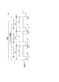
- FIG. 10 shows changes in the waveform of the scanning signal, the on / off state of the target LED, and the transmittance of the pixel in two consecutive fields (the preceding field and the following field).
- P1 represents a pixel on the first row
- Pj represents a pixel on the (m / 2) th row
- Pm represents a pixel on the mth row (final row).
- the light guide plate 72 is configured so that the light output toward the liquid crystal panel 800 gradually increases from the upper part of the panel toward the lower part of the panel. The difference in brightness between the two is suppressed.
- the liquid crystal response time is 2 milliseconds
- video data is still written in the subsequent field after 2 milliseconds from the start time of the black writing period T2 of the preceding field, that is, 1 millisecond after the start time of the subsequent field.
- the transmittance reaches the black level. If the transmittance has reached the black level, the display of the previous field is not affected, so that the target LED can be brought into a light emitting state. Therefore, the black writing period T2 and the backlight emission period T3 are set such that the length from the start time of the black writing period T2 in each field to the start time of the backlight emission period T3 in the next field is longer than the liquid crystal response time. And are set.
- the start time of the black writing period T2 is a time one millisecond before the end time of each field, a quarter field period (1.39) from the start time of each field.
- the target LED is turned on. Focusing on the first row, the writing of video data is started before a sufficient time has elapsed from the start of the black writing period T2. Therefore, in order to more reliably prevent the occurrence of color mixing, it is preferable to set the target LED in the light emitting state after the liquid crystal response time (here, 2 milliseconds) has elapsed from the start time of each field.
- the target LED is in the light emitting state during the black writing period T2, but the present invention is not limited to this, and the target LED may be turned off in the black writing period T2. That is, in each field, the end point of the backlight emission period T3 may be set earlier than the start point of the black writing period T2. However, even if the target LED is made to emit light during the black writing period T2, no color mixing occurs due to this. Further, in order to increase the brightness of the screen, the backlight emission period T3 is preferably long. Therefore, in the present embodiment, the target LED is in a light emitting state even during the black writing period T2.
- Black writing period In this embodiment, the period during which the scanning signal is on level (high level) for writing video data (one horizontal scanning period) is several microseconds, whereas the scanning signal is on for black writing.
- the period of time (high level) (black writing period T2) is set to 1 millisecond. The reason for this will be described below.
- the “liquid crystal step response” When writing to the pixel capacitor 66 is performed, the TFT 60 is turned on / off in each pixel formation portion 6. When the TFT 60 is turned off, the charge accumulated in the pixel electrode 61 is held. However, since the response of the liquid crystal is not completed in a very short time, the liquid crystal continues to respond by the electric field even after the TFT 60 changes from the on state to the off state.
- the start time of the black writing period T2 is set to 1 millisecond before the end time of each field. Even so, there is a high possibility that the transmittance does not reach the black level in all the pixels.
- the voltage is maintained even when the capacitance changes, and thus the transmittance approaches the target value (here, the black level). Therefore, if the black writing period T2 is lengthened, the transmissivity at the end of each field becomes a value closer to the black level, so that the change in capacitance after the end of the black writing period T2 becomes small.
- the length of the black writing period T2 is set to 1 millisecond.
- the LED 71 is provided only on the lower side of the liquid crystal panel 800 as a backlight light source. Further, no reflection wall or the like is provided in the liquid crystal panel 800. For this reason, the display part 600 can be made transparent. In each field constituting one frame period, video data is written to all the pixel capacitors 66 only in the first half period, and black writing (black display) to all the pixel capacitors 66 is performed in a part of the second half. Data is written). The LED 71 is in a light emitting state when a quarter field period has elapsed from the start of each field.
- the LED 71 enters a light emitting state after a sufficient time has elapsed for the transmittance of the pixel to reach the black level.
- each field is not affected by the display of the previous field, and color mixing is prevented.
- the target display image is an image as shown in FIG. 27, the image visually recognized by the human eye is almost the image as shown in FIG.
- a liquid crystal display device capable of displaying an image while the background is in a transmissive state
- color mixing is performed while adopting a configuration in which an edge light type backlight is provided on one side of the panel. It is possible to perform field sequential driving without generating the above.
- the second method (method in which writing of video data is completed in the first half period in each field and the backlight is emitted only in the second half period of each field)
- the backlight emission period is such a short period, a light source having an extremely strong light emission power is required to perform display with sufficient luminance. It is also conceivable to extend the backlight emission period by causing the backlight to emit light when the liquid crystal responds to some extent so that the visually recognized image (image visually recognized by the human eye) is at an acceptable level.
- the backlight emission period is expected to be about 1.39 milliseconds (the last quarter period of each field).
- a backlight emission period T3 having a sufficient length (4.17 milliseconds) can be ensured, so that a good display quality can be obtained without reducing the color purity.
- the length of the black writing period T2 is 1 millisecond (assuming that the liquid crystal response time is 2 milliseconds), without depending on the liquid crystal step response, By the time the next field is displayed, the transmittance at each pixel is sufficiently close to the black level. Therefore, the occurrence of color mixing is effectively suppressed.
- one frame period is composed of three fields for displaying a red screen, a green screen, and a blue screen, respectively.
- the present invention is not limited to this.
- modified examples of the configuration of one frame period will be described.
- the frame rate conversion unit 100 receives an input image signal DIN of 60 Hz, and data of 480 Hz is output from the frame rate conversion unit 100 as target image data DAT.
- video data is written in each field constituting one frame period only in the first half period (a period of one-half length of one field). Therefore, in this modification, the driving frequency of the liquid crystal panel is 480 Hz, but the number of fields that appear in one second is 240.
- FIG. 11 is a diagram showing a configuration of one frame period in the present modification.
- one frame period is composed of four fields (first to fourth fields).
- one frame period is 16.7 milliseconds and one field period is about 4.18 milliseconds.
- the first field is a field in which red screen writing (charging) and red screen display are performed.
- the second field is a field where green screen writing and green screen display are performed.
- the third field is a field where blue screen writing and blue screen display are performed.
- the fourth field is a field where white screen writing and white screen display are performed.
- a video data writing period T1, a black writing period T2, and a backlight emission period T3 are provided as in the first embodiment.
- the LEDs 71 of all the colors RGB are in a light emission state.
- the liquid crystal panel 800 is irradiated with white light by causing the red LED 71 (R), the green LED 71 (G), and the blue LED 71 (B) to emit light.
- the LEDs 71 of all these colors are displayed in the fourth field.
- the light emission state is set.
- FIG. 12 is a diagram showing a configuration of one frame period in the present modification.
- one frame period is composed of three fields (first to third fields) as in the first embodiment.
- the LEDs 71 of a plurality of colors are in a light emitting state in each field.
- the color of the LED 71 that is in the light emission state in each field depends on the target display image.
- the present invention can also be applied to a case where one frame period is configured by four or more fields in which the LEDs 71 of a plurality of colors are in a light emitting state.
- the LEDs 71 of a plurality of colors are in a light emitting state in each field. For this reason, in addition to the effect similar to the said 1st Embodiment, the effect that generation
- Second Embodiment> In the first embodiment, it is assumed that the liquid crystal display device can operate at a driving frequency of 360 Hz. However, sufficient display quality may not be obtained due to insufficient writing period. Thus, in the present embodiment, by adopting a configuration in which video data is written in three rows at a time, it is possible to write video data in all the pixel capacitors 66 only in the first half of each field. Yes. Note that the present invention can also be applied to a configuration in which video data is written every two rows or a configuration in which video data is written every four or more rows.
- FIG. 13 is a diagram illustrating a configuration in the display unit 600 according to the present embodiment.
- three source bus lines are provided for each column.
- Three source bus lines indicated by symbols SLia, SLib, and SLic are provided in the i-th column, where i is an integer from 1 to n.
- the pixel formation unit 6 in the first row is connected to the source bus line SLia
- the pixel formation unit 6 in the second row is connected to the source bus line SLib
- the pixel formation unit 6 in the third row is connected to the source bus line SLic.
- the same connection relationship as in the first to third lines is repeated for every three lines.
- FIG. 14 is a block diagram showing a schematic configuration of the gate driver 400 in the present embodiment.
- the gate driver 400 includes a shift register 410 including (m / 3) flip-flop circuits 41 and a black writing control unit 420 for controlling black writing.
- the black writing control unit 420 is provided with (m / 3) OR circuits 42 so as to correspond to the flip-flop circuits 41 in the shift register 410 on a one-to-one basis.
- the output signal from the flip-flop circuit 41 and the black writing control signal GBL are input to the OR circuit 42.
- the output signal from the OR circuit 42 is given to the gate bus line GL as a scanning signal.
- the gate driver 400 is configured such that an output signal from one OR circuit 42 is supplied to three gate bus lines GL.
- an output signal from the OR circuit 42 provided corresponding to the third-stage flip-flop circuit 41 is applied to the three gate bus lines GL7 to GL9.
- the gate driver 400 configured as described above is supplied with the gate start pulse signal GSP, the gate clock signal GCK, and the black writing control signal GBL, as in the first embodiment. Accordingly, three active scan signals are sequentially applied to the m gate bus lines GL1 to GLm in the first half period of each field. Also, active scanning signals are applied simultaneously to the m gate bus lines GL1 to GLm during a part of the latter half of each field.
- FIG. 15 is a block diagram showing a schematic configuration of the source driver 300 in the present embodiment.
- the source driver 300 includes a shift register 310 including n flip-flop circuits 31, a sampling unit 320 including (n ⁇ 3) sampling circuits 32 for sampling the digital video signal DV based on the sampling pulse, and , And an output unit 330 that outputs a driving video signal.
- the shift register 310 is configured such that the source start pulse signal SSP is supplied to the first-stage flip-flop circuit 31 and the source clock signal SCK is supplied to all the flip-flop circuits 31 in common.
- the pulse of the source start pulse signal SSP is given to the first stage flip-flop circuit 31 of the shift register 310, the pulse included in the source start pulse signal SSP is changed based on the source clock signal SCK.
- To the n-th flip-flop circuit 31 sequentially.
- sampling pulses SAM1 to SAMn are sequentially output from the 1st to m-th stage flip-flop circuits 31.
- the sampling unit 320 is supplied with a digital video signal DV and sampling pulses SAM1 to SAMn.
- a digital video signal corresponding to the source bus line SLia is denoted by a symbol DVa
- a digital video signal corresponding to the source bus line SLib is denoted by a symbol DVb
- a digital corresponding to the source bus line SLic is represented.
- the video signal is denoted by the symbol DVc.
- the sampling circuit 32 the digital video signal DV is sampled based on the sampling pulse. In this embodiment, every time one sampling pulse is output from the shift register 310, the sampling unit 320 samples three digital video signals DVa, DVb, and DVc.
- the digital video signals DV for three rows are held.
- the held digital video signal DV is converted into an analog voltage at the timing when the pulse of the latch strobe signal LS is generated.
- the converted analog voltage is simultaneously applied from the output unit 330 to the source bus line SL as a driving video signal.
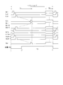
- FIG. 16 is a timing chart for explaining a driving method in the present embodiment.
- m gate bus lines GL1 to GLm are sequentially driven three by three.
- a driving video signal as video data is (n ⁇ 3) Applied to one source bus line SL.
- video data is written by three rows in a video data writing period (a period until a half field period elapses from the start time of each field) T1.
- the writing of the video data to all the pixel capacitors 66 in the display unit 600 is completed only in the first half period.
- the black writing period the last several milliseconds of each field
- data black voltage
- the LED driver 500 causes the target LED to emit light.
- a liquid crystal display device capable of displaying an image while the background is in a transmissive state
- display is performed while adopting a configuration in which an edge light type backlight is provided on one side of the panel.
- Field sequential driving can be performed without degrading quality or mixing colors.
- N is an integer of 2 or more, and N source bus lines are provided for each column, so that video data can be written by N rows.
- the number of source bus lines per column is increased, so that the aperture ratio of the panel is lowered. Therefore, it is preferable to reduce the number of lines to which video data is simultaneously written as much as possible without causing insufficient charging. Thereby, the fall of the aperture ratio of a panel is suppressed.
- the video data is written in three rows from the upper side of the panel toward the lower side of the panel.
- the panel may be logically divided into three areas, and video data may be written simultaneously in these three areas. This configuration will be described below.
- area A the area from the 1st to kth rows is referred to as “area A”
- area B the area from the (k + 1) to 2kth rows is referred to as “area B”
- area C the area from the (2k + 1) th to mth lines.
- area C the area from the 1st to kth rows.
- FIG. 18 is a block diagram showing a schematic configuration of the gate driver 400 in this modification.
- the first shift register 410 (1) corresponding to the area A and the first shift register 410 (1) are configured so that simultaneous video data writing can be performed in three areas (area A, area B, and area C).
- a second shift register 410 (2) corresponding to the region B and a third shift register 410 (3) corresponding to the region C are provided in the gate driver 400.
- the gate start pulse signal GSP is given to the flip-flop circuit 41 corresponding to the first row, the flip-flop circuit 41 corresponding to the 2k row, and the flip-flop circuit 41 corresponding to the (2k + 1) th row.
- the flip-flop circuit 41 corresponding to the first row is included in the first shift register 410 (1), and the flip-flop circuit 41 corresponding to the 2kth row is included in the second shift register 410 (2). ) The flip-flop circuit 41 corresponding to the row is included in the third shift register 410 (3).
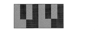
- the gate bus lines GL1 to GLm are driven in the video data writing period T1, as shown in FIG. That is, in the video data writing period T1, video data is sequentially written row by row from the upper side of the panel to the lower side of the panel in the regions A and C, and from the lower side of the panel to the upper side of the panel in the region B. The video data is sequentially written row by row. The video data is written in three regions (region A, region B, and region C) simultaneously and in parallel.
- the transmittance decreases in the region A and the region C as it approaches the panel lower side, and the transmittance decreases in the region B as it approaches the panel upper side. Therefore, in the present modification, the light guide plate 72 is configured so that the light output from the light guide plate 72 to the liquid crystal panel 800 side becomes a curve indicated by reference numeral 78 in the graph shown in FIG. Thereby, generation
- the panel is logically divided into three areas, but the panel may be logically divided into two areas or four or more areas. Specifically, regardless of the number of divisions, the area in the display unit 600 is logically divided into a plurality of areas so that the areas defined as the first areas and the areas defined as the second areas appear alternately. be able to.
- the light guide plate 72 may be configured as follows so that video data writing and black writing are performed as follows.
- the intensity of light given to the liquid crystal panel 800 gradually increases as it approaches the lower end from the upper end of the liquid crystal panel 800
- the light guide plate 72 is configured so that the intensity of light given to the liquid crystal panel 800 gradually increases as it approaches the upper end from the lower end of the liquid crystal panel 800 when each color LED 71 is in a light emitting state.
- the writing of the video data is sequentially performed in a plurality of lines from the upper part of the panel to the lower part of the panel, and in the second area, the plurality of lines is sequentially performed from the lower part of the panel to the upper part of the panel. To be done. Black writing is performed at the same timing in all rows.
- Third Embodiment> ⁇ 3.1 Overall configuration and backlight configuration> Since the overall configuration and the configuration of the backlight 700 are substantially the same as those in the first embodiment (see FIGS. 2 and 4 to 6), only differences from the first embodiment will be described.
- the frame rate conversion unit 100 is supplied with an input image signal DIN of 60 Hz, and data of 540 Hz is output from the frame rate conversion unit 100 as target image data DAT.
- the video data is written only in a period from the start of each field until a third field period elapses. Therefore, in this embodiment, the driving frequency of the liquid crystal panel is 540 Hz, but the number of fields that appear in one second is 180.
- the black write control signal GBL provided from the signal processing circuit 200 to the gate driver 400 in the first embodiment is not necessary.
- the light guide plate 72 in the backlight 700 is configured so that the light output to the liquid crystal panel 800 side becomes uniform as a whole (see FIG. 21).
- FIG. 22 is a schematic diagram showing the configuration of the gate driver 400 in the present embodiment.
- the gate driver 400 in the present embodiment is configured by a shift register 410 composed of m flip-flop circuits 41, like a gate driver having a general configuration. Further, the black driver 420 is not provided in the gate driver 400.
- the source driver 300 can employ a known configuration.
- the video data writing period T1 is a period from the start of each field until the one-third field period elapses.
- a gate start pulse signal GSP having a waveform as shown in FIG. 23 is supplied to the gate driver 400 having the above-described configuration.
- a pulse indicated by reference numeral 92 is a pulse for writing video data
- a pulse indicated by reference numeral 93 is a pulse for black writing.
- the gate bus lines GL1 to GLm are driven as shown in FIG.
- ON / OFF of object LED is controlled similarly to the said 1st Embodiment.
- the light guide plate 72 is configured so that the light output from the light guide plate 72 to the liquid crystal panel 800 side becomes uniform as a whole (see FIG. 21).
- the video data is written only in the period from the start of each field until the one-third field period elapses, and black writing is performed in the latter half of the period. Done.
- the target LED is in a light emitting state from the time when a predetermined period has elapsed from the start of each field to the end of the field. Note that this predetermined period is set to a time sufficient for the pixel transmittance to reach the black level.
- black writing is performed for each field period in the liquid crystal display device that performs field sequential driving.
- each field is not affected by the display of the previous field, and color mixing is prevented. That is, in a liquid crystal display device capable of displaying an image while the background is in a transmissive state, field sequential driving is performed without causing color mixing while adopting a configuration in which an edge light type backlight is provided on one side of the panel. Is possible.
- black writing is sequentially performed row by row from the upper part of the panel toward the lower part of the panel, so that the transmittance does not differ between the upper part of the panel and the lower part of the panel. Therefore, the deterioration of display quality is suppressed, and the configuration of the light guide plate 72 is simplified as compared with the first embodiment.
- video data writing and black writing are sequentially performed row by row, but the present invention is not limited to this.
- the video data can be written in a plurality of rows, and the black data can be written in a plurality of rows.
- N N is an integer of 2 or more
- video signal lines are provided for each column of the pixel matrix, so that video data is sequentially written into the pixel capacitor 66 by N rows, and the pixel capacitor.
- the liquid crystal panel driver (the gate driver 400 and the source driver 300) performs the gate writing to the gate bus line GL and the source bus so that the black writing to 66 is sequentially performed N rows in the same order as the video data writing to the pixel capacitor 66
- the line SL can be driven.
- the waveform of the scanning signal applied to the gate bus lines GL1 to GLm is, for example, as shown in FIG.
- video data is written to the pixel capacitors by a plurality of rows, so that the writing period to each pixel capacitor 66 can be lengthened.
- a plurality of video signal lines SL, a plurality of scanning signal lines GL, and a plurality of rows and a plurality of columns of pixel matrices are provided corresponding to the intersections of the plurality of video signal lines SL and the plurality of scanning signal lines GL.
- Writing to the liquid crystal panel 800 capable of displaying an image while making the background transparent on the display unit 600 including the plurality of pixel forming units 6 and the plurality of pixel capacitors 66 included in the plurality of pixel forming units 6 is performed.
- a liquid crystal panel driving unit (300, 400) for driving the plurality of video signal lines SL and the plurality of scanning signal lines GL, a backlight 700 provided on the back side of the liquid crystal panel 800, and the backlight And a backlight driving unit 500 for driving 700, by dividing one frame period into a plurality of fields and displaying a screen of a different color for each field.
- the backlight 700 includes: A plurality of light sources 71 including a light source of K color (K is an integer of 3 or more) provided near one side of the liquid crystal panel 800 in a direction in which the plurality of video signal lines SL extend; A light guide plate 72 for guiding the light emitted from the plurality of light sources 71 to the liquid crystal panel 800;
- the liquid crystal panel driving unit (300, 400) is for black display to the plurality of pixel capacitors 66 so that video data is written to the plurality of pixel capacitors 66 during the first half of each field.
- the backlight driving unit 500 is included in the first half of each field from the start time of each field.
- the first time point is such that the length of the period from the third time point at which writing of black display data starts in each field to the first time point in the next field is longer than the liquid crystal response time.
- the liquid crystal display device is characterized in that the third time point is set.
- the video data is written to all the pixel capacitors 66 only in the first half period, and in all the pixel capacitors in the second half period.
- Data for black display is written to 66.
- the light source 71 enters a light emitting state. Therefore, each field is not affected by the display of the previous field, and color mixing is prevented.
- the light source 71 is provided on one side of the liquid crystal panel 800.
- the light guide plate 72 includes the light source 71 of each color. Is configured to gradually increase the intensity of light given to the liquid crystal panel 800 as it approaches the first side from the second side when
- the liquid crystal panel driving unit (300, 400) is configured to sequentially write video data to the plurality of pixel capacitors 66 from the second side to the first side, and Driving the plurality of video signal lines SL and the plurality of scanning signal lines GL so that writing of black display data to the pixel capacitor 66 is performed at the same timing in all the rows of the pixel matrix.
- the liquid crystal display device according to appendix 1 which is characterized.
- the transmittance decreases as it approaches the first side (the side where writing is performed last) from the second side (the side where writing is performed first) of the liquid crystal panel 800.
- the light guide plate 72 is configured so that the intensity of light given to the liquid crystal panel 800 gradually increases from the second side to the first side.
- N video signal lines SL N is an integer of 2 or more
- the liquid crystal panel driving unit (300, 400) is configured to sequentially write video data to the plurality of pixel capacitors 66 every N rows and to display black data to the plurality of pixel capacitors 66.
- video data is written to the pixel capacitor 66 by a plurality of rows. For this reason, it becomes possible to lengthen the writing period to each pixel capacitor 66, and the deterioration of display quality due to insufficient charging is prevented.
- the light guide plate 72 includes the light source 71 of each color. Is configured to gradually increase the intensity of light given to the liquid crystal panel 800 as it approaches the first side from the second side when 4.
- the region in the display unit 600 is logically divided into a plurality of regions so that regions defined as first regions and regions defined as second regions appear alternately,
- the one side portion and the other side portion of the liquid crystal panel 800 in the extending direction of the plurality of video signal lines SL are defined as a first side portion and a second side portion, respectively, the light guide plate 72 includes the first region.
- the intensity of light given to the liquid crystal panel 800 gradually increases as the distance from the second side approaches the first side, and the first In the two regions, when the light sources 71 of the respective colors are in a light emitting state, the intensity of light given to the liquid crystal panel 800 is gradually increased as it approaches the second side from the first side, In the first region, video data is written to the plurality of pixel capacitors 66 sequentially from the second side portion to the first side portion, and in the second region, the plurality of pixels are written. 4. The liquid crystal display device according to appendix 3, wherein video data is written to the capacitor 66 sequentially from the first side portion toward the second side portion.
- the same effect as the configuration described in Supplementary Note 3 can be obtained by a configuration in which the region in the display unit 600 is logically divided into a plurality of regions.
- the light guide plate 72 is configured such that the intensity of light applied to the liquid crystal panel 800 is uniform throughout the display unit 600.
- the liquid crystal panel drive unit (300, 400) writes video data to the plurality of pixel capacitors 66 sequentially, and writes black display data to the plurality of pixel capacitors 66.
- Appendix 1 is characterized in that the plurality of video signal lines SL and the plurality of scanning signal lines GL are driven so as to be sequentially performed in the same order as the writing of the video data to the plurality of pixel capacitors 66.
- the black display data is sequentially written to the pixel capacitor 66 in the same order as the video data is written to the pixel capacitor 66. For this reason, the transmittance does not differ between the upper part of the panel and the lower part of the panel. Therefore, the deterioration of display quality is suppressed, and the same effect as the configuration described in Appendix 1 can be obtained without complicating the configuration of the light guide plate 72.
- Appendix 7 The liquid crystal display device according to appendix 6, wherein the video data is written into the plurality of pixel capacitors 66 from the start of each field until a third field period elapses.
- the light guide plate 72 is configured such that the intensity of light applied to the liquid crystal panel 800 is uniform throughout the display unit 600.
- N video signal lines SL (N is an integer of 2 or more) are provided for each column of the pixel matrix,
- the liquid crystal panel driving unit (300, 400) is configured to sequentially write video data to the plurality of pixel capacitors 66 every N rows and to display black data to the plurality of pixel capacitors 66.
- the plurality of video signal lines SL and the plurality of scanning signal lines GL are driven so that the writing is sequentially performed in N rows in the same order as the writing of the video data to the plurality of pixel capacitors 66.
- the liquid crystal display device according to appendix 1.
- the first time point is a time point when a quarter field period has elapsed from the start time of each field,
- the light source 71 is maintained in a light emitting state for a sufficiently long period. For this reason, the same effect as the configuration described in Supplementary Note 1 can be obtained without causing insufficient luminance.
- the transmittance in each pixel is sufficiently close to the black level before the display in the next field is performed without depending on the step response of the liquid crystal. For this reason, the occurrence of color mixing is effectively suppressed.
- the light source 71 is turned off during the period from the start of each field until the liquid crystal response time elapses. For this reason, the occurrence of color mixing is reliably prevented.
- the light source 71 is turned off during a period in which black display data is written. For this reason, power consumption is reduced.
- the K-color light source 71 is a three-color light source including a red light source 71 (R), a green light source 71 (G), and a blue light source 71 (B). Liquid crystal display device.
- One frame period is composed of three fields including a field corresponding to a red screen, a field corresponding to a green screen, and a field corresponding to a blue screen.
- the backlight driver is When displaying the red screen, the red light source 71 (R) is in a light emitting state, When displaying the green screen, the green light source 71 (G) is turned on, The liquid crystal display device according to appendix 13, wherein when the blue screen is displayed, the blue light source 71 (B) is in a light emitting state.
- One frame period is composed of four fields including a field corresponding to a red screen, a field corresponding to a green screen, a field corresponding to a blue screen, and a field corresponding to a white screen.
- the backlight driver is When displaying the red screen, the red light source 71 (R) is in a light emitting state, When displaying the green screen, the green light source 71 (G) is turned on, When displaying the blue screen, the blue light source 71 (B) is in a light emitting state, Appendix 13 is characterized in that when the white screen is displayed, the red light source 71 (R), the green light source 71 (G), and the blue light source 71 (B) are in a light emitting state.
- one frame period is composed of three fields corresponding to the screens of the three primary colors and fields corresponding to the white screen.
- the red light source 71 (R), the green light source 71 (G), and the blue light source 71 (B) are sequentially turned on, the light sources 71 of all the colors are turned on.
- production of the color breakage in the case of a moving image display can be suppressed is acquired.
- Appendix 16 The liquid crystal display device according to appendix 1, wherein the backlight driving unit 500 causes the light sources 71 of a plurality of colors to emit light in each field in order to display a screen having a color corresponding to each field. .
- the light sources 71 of a plurality of colors are in a light emitting state in each field constituting one frame period. For this reason, in addition to the effect similar to the structure of Additional remark 1, the effect that generation
- Each pixel forming portion 6 has a control terminal and two conduction terminals, and the control terminal is connected to the corresponding scanning signal line GL as a switching element for controlling writing to each pixel capacitor 66.
- a thin film transistor in which a channel layer is formed of an oxide semiconductor is used as the thin film transistor 60 provided in the liquid crystal panel 800. For this reason, in addition to obtaining the effect of high definition and low power consumption, the writing speed can be increased as compared with the prior art.
- a plurality of video signal lines SL, a plurality of scanning signal lines GL, and a plurality of rows and a plurality of columns of pixel matrices are provided corresponding to the intersections of the plurality of video signal lines SL and the plurality of scanning signal lines GL.
- a display unit 600 including a plurality of pixel forming units 6 includes a liquid crystal panel 800 capable of displaying an image while making the background transparent, and a backlight 700 provided on the back side of the liquid crystal panel 800.
- a method of driving a liquid crystal display device that displays a color image by dividing a period into a plurality of fields and displaying a screen of a different color for each field, A liquid crystal panel driving step of driving the plurality of video signal lines SL and the plurality of scanning signal lines GL in order to perform writing to the plurality of pixel capacitors 66 included in the plurality of pixel forming units 6; A backlight driving step of driving the backlight 700;
- the backlight 700 includes: A plurality of light sources 71 including a light source of K color (K is an integer of 3 or more) provided near one side of the liquid crystal panel 800 in a direction in which the plurality of video signal lines SL extend; A light guide plate 72 for guiding the light emitted from the plurality of light sources 71 to the liquid crystal panel 800;
- video data is written to the plurality of pixel capacitors 66 during the first half of each field, and black display data is written to the plurality of pixel capacitors 66.
- the plurality of video signal lines SL and the plurality of scanning signal lines GL are driven so as to be performed in a part of the second half of each field,
- the backlight driving step includes the first light source 71 included in the first half of each field from the start time of each field.
- the target light source is maintained in an extinguished state during a period up to one time point, and the target light source is maintained in a light emitting state during a period from the first time point to a second time point included in the second half of each field,
- the first time point is such that the length of the period from the third time point at which writing of black display data starts in each field to the first time point in the next field is longer than the liquid crystal response time.
- the third time point is set.
Landscapes
- Engineering & Computer Science (AREA)
- Chemical & Material Sciences (AREA)
- Crystallography & Structural Chemistry (AREA)
- Physics & Mathematics (AREA)
- Computer Hardware Design (AREA)
- General Physics & Mathematics (AREA)
- Theoretical Computer Science (AREA)
- Liquid Crystal Display Device Control (AREA)
- Control Of Indicators Other Than Cathode Ray Tubes (AREA)
- Liquid Crystal (AREA)
Abstract
背景を透過状態にしつつ画像表示を行うことのできる液晶表示装置において、パネルの1辺側にエッジライト型バックライトを備えるという構成を採用しつつ混色を生ずることなくフィールドシーケンシャル駆動を行う。 全ての画素容量への映像データの書き込みが各フィールドの前半の期間(T1)に行われるように、かつ、全ての画素容量への黒書き込みが各フィールドの後半の一部の期間(T2)に行われるように、ソースバスラインおよびゲートバスラインを駆動する。バックライトは、液晶パネルの下部側のみに設けられる。ここで、1フレーム期間を構成する各フィールドにおいて黒書き込み開始時点(第3時点)から次のフィールドにおけるバックライト発光期間の開始時点(第1時点)までの期間の長さが液晶応答時間よりも長くなるように、第1時点および第3時点が設定される。
Description
本発明は、液晶表示装置に関し、特に、画面の向こう側を見ることができる液晶表示装置に関する。
一般に、カラー表示を行う液晶表示装置では、1つの画素は、赤色光を透過するカラーフィルタが設けられた赤色画素,緑色光を透過するカラーフィルタが設けられた緑色画素,および青色光を透過するカラーフィルタが設けられた青色画素の3つのサブ画素に分割されている。これら3つのサブ画素に設けられたカラーフィルタによってカラー表示が可能となっているが、液晶パネルに照射されるバックライト光の約2/3がカラーフィルタで吸収される。このため、カラーフィルタ方式の液晶表示装置は光利用効率が低いという問題を有する。そこで、カラーフィルタを用いずにカラー表示を行うフィールドシーケンシャル駆動を採用する液晶表示装置が注目されている。
フィールドシーケンシャル駆動を採用する一般的な液晶表示装置では、1画面の表示期間(1フレーム期間)は3つのフィールド(第1~第3フィールド)に分割されている。なお、フィールドはサブフレームとも呼ばれるが、以下の説明では、統一してフィールドの語を用いる。例えば、第1フィールドでは、入力信号の赤色成分に基づいて赤色の画面が表示され、第2フィールドでは、入力信号の緑色成分に基づいて緑色の画面が表示され、第3フィールドでは、入力信号の青色成分に基づいて青色の画面が表示される。以上のようにして1つずつ原色を表示することにより、液晶パネルにカラー画像が表示される。このようにしてカラー画像の表示が行われるので、フィールドシーケンシャル駆動を採用する液晶表示装置ではカラーフィルタが不要となる。これにより、フィールドシーケンシャル駆動を採用する液晶表示装置では、カラーフィルタ方式の液晶表示装置に比べて光利用効率が約3倍になる。
ところで、一般に、アクティブマトリクス型の液晶表示装置では、液晶パネルに設けられている複数本のゲートバスライン(走査信号線)は1本ずつ順次に駆動される。このため、パネル上部の画素については画素容量への映像データの書き込み(充電)は各フィールドの開始付近に行われ、パネル中央部の画素については画素容量への映像データの書き込み(充電)は各フィールドの中頃に行われ、パネル下部の画素については画素容量への映像データの書き込み(充電)は各フィールドの終了付近に行われる。従って、フィールドシーケンシャル駆動を採用する場合には、パネル上部からパネル下部へと順次に走査が行われるのに同期してバックライトを発光させる必要がある。なお、以下においては、パネル上部からパネル下部へとバックライトを順次に発光させる処理のことを「バックライトスキャン」という。
しかしながら、バックライトスキャンを行うことができない構成を採用せざるを得ない場合もある。この場合、フィールドシーケンシャル駆動が行われると、混色が生じた画像が人の目に視認されてしまう。これについて、以下に説明する。なお、本明細書では、混色とは、異なる色の光が不必要に混ざり合うことを意味する。
バックライトスキャンを行うことができないエッジライト型バックライトを用いてフィールドシーケンシャル駆動を行う場合の従来の手法(以下、「第1の手法」という。)について説明する。なお、バックライト光源としてはLED(発光ダイオード)が採用されているものとする。第1の手法においては、1フレーム期間は、図26に示すように、赤色の画面を表示するための第1フィールドと緑色の画面を表示するための第2フィールドと青色の画面を表示するための第3フィールドとに分割されている。図26において、各波形のハイの部分が「発光状態」を表し、各波形のローの部分が「消灯状態」を表している(これは、図1,図8~図12,図16,図19,図24~図26,および図41においても同様である)。第1フィールドでは、赤色のLED(R-LED)が1フィールド期間を通じて発光状態(点灯状態)とされる。第2フィールドでは、緑色のLED(G-LED)が1フィールド期間を通じて発光状態とされる。第3フィールドでは、青色のLED(B-LED)が1フィールド期間を通じて発光状態とされる。このような構成において、目標表示画像が図27に示すような画像であれば、第1フィールドにおける目標表示画像は図28に示すような画像となり、第2フィールドにおける目標表示画像は図29に示すような画像となり、第3フィールドにおける目標表示画像は図30に示すような画像となる。
ところで、各画素において、液晶に電圧が印加されてから目標とする透過率に到達するまでには数ミリ秒から十数ミリ秒程度の時間を要する。この点とゲートバスラインが1本ずつ順次に駆動される点とを考慮すると、第1の手法では、1フレーム期間中の各時点(図26参照)における表示画像は以下のようになる。第1フィールドにおいて、時点t81,時点t82,および時点t83における表示画像はそれぞれ図31、図32,および図33に示すような画像となる。第2フィールドにおいて、時点t84,時点t85,および時点t86における表示画像はそれぞれ図34、図35,および図36に示すような画像となる。第3フィールドにおいて、時点t87,時点t88,および時点t89における表示画像はそれぞれ図37、図38,および図39に示すような画像となる。その結果、第1の手法によれば、人の目によって視認される画像は、図40に示すように混色が生じた画像となる。
そこで、上述のような混色の発生を抑制するために、各フィールドにおいて前半の期間に映像データの書き込みを終了させて各フィールドの後半の期間のみにバックライト光源を発光させる手法(以下、「第2の手法」という。)が提案されている(図41参照)。この第2の手法によれば、各フィールドにおいて1つ前のフィールドの状態が人の目に視認されることが抑制される。すなわち、混色の発生が抑制される。
なお、本件発明に関連して、以下の先行技術文献が知られている。日本の特開2012-109227号公報には、直下型バックライトを用いてバックライトスキャンを行う表示装置の発明が開示されている。また、日本の特開2012-27452号公報には、各フィールドにおいて後半の期間のみにバックライト光源を発光させる手法(上記第2の手法)を採用した液晶表示装置の発明が開示されている。この液晶表示装置では、パネル内の領域を論理的に3つの領域に分割して、当該3つの領域で同時並行的に映像データの書き込みを行うことによって、各フィールドにおける映像データの書き込み期間を従来よりも短くしている。
ところで、近年、背景を透過状態にしつつ画像表示を行うことのできる表示装置(画面の向こう側を見ることができる表示装置)の開発が進められている。このような表示装置は「シースルーディスプレイ」,「透明ディスプレイ」などと呼ばれている。シースルーディスプレイにおいては、表示部を透明にする必要がある。このため、シースルーディスプレイでフィールドシーケンシャル駆動を採用する場合には、直下型バックライトを用いてバックライトスキャンを行うという構成(日本の特開2012-109227号公報に開示された構成)を採用することができない。
また、シースルーディスプレイに関しては、デザイン性が比較的重視される。この点を考慮すると、「パネルの3辺には額縁を設けず、パネルの1辺のみに額縁を設け、その額縁が設けられた1辺側にエッジライト型バックライトを備える」という構成が好ましい。
また、第2の手法によれば、以下に説明するように、パネル下部での混色の発生を充分に抑制することができない。第2の手法では、1フレーム期間中の各時点(図41参照)における表示画像は例えば以下のようになる。第1フィールドにおいて、時点t91および時点t92における表示画像はそれぞれ図42および図43に示すような画像となる。第2フィールドにおいて、時点t93および時点t94における表示画像はそれぞれ図42および図44に示すような画像となる。第3フィールドにおいて、時点t95および時点t96における表示画像はそれぞれ図42および図45に示すような画像となる。その結果、第2の手法によれば、人の目によって視認される画像は、図46に示すようにパネル下部で混色が生じた画像となる。さらに、日本の特開2012-27452号公報に開示された発明によれば、パネル内の領域の分割数に応じてソースバスラインの本数を増やす必要があるので、パネルの開口率の低下(透過率の低下)が懸念される。
そこで本発明は、背景を透過状態にしつつ画像表示を行うことのできる液晶表示装置において、パネルの1辺側にエッジライト型バックライトを備えるという構成を採用しつつ混色を生ずることなくフィールドシーケンシャル駆動を行うことを目的とする。
本発明の第1の局面は、複数の映像信号線,複数の走査信号線,および前記複数の映像信号線と前記複数の走査信号線との交差点に対応して設けられ複数行×複数列の画素マトリクスを形成する複数の画素形成部を含む表示部に背景を透過状態にしつつ画像を表示することができる液晶パネルと、前記複数の画素形成部に含まれる複数の画素容量への書き込みを行うために前記複数の映像信号線および前記複数の走査信号線を駆動する液晶パネル駆動部と、前記液晶パネルの背面側に設けられたバックライトと、前記バックライトを駆動するバックライト駆動部とを備え、1フレーム期間を複数のフィールドに分割してフィールド毎に異なる色の画面を表示することによってカラー画像の表示を行う液晶表示装置であって、
前記バックライトは、
前記複数の映像信号線が延びる方向についての前記液晶パネルの一側部近傍に設けられた、K色(Kは3以上の整数)の光源を含む複数の光源と、
前記複数の光源から出射された光を前記液晶パネルに導くための導光板と
を有し、
前記液晶パネル駆動部は、前記複数の画素容量への映像データの書き込みが各フィールドの前半の期間に行われるように、かつ、前記複数の画素容量への黒表示用のデータの書き込みが各フィールドの後半の一部の期間に行われるように、前記複数の映像信号線および前記複数の走査信号線を駆動し、
各フィールドに対応する色の画面を表示するために発光状態とされるべき光源を対象光源と定義したとき、前記バックライト駆動部は、各フィールドの開始時点から各フィールドの前半に含まれる第1時点までの期間には前記対象光源を消灯状態で維持し、前記第1時点から各フィールドの後半に含まれる第2時点までの期間には前記対象光源を発光状態で維持し、
各フィールドにおいて黒表示用のデータの書き込みが開始される時点である第3時点から次のフィールドにおける前記第1時点までの期間の長さが液晶応答時間よりも長くなるように、前記第1時点および前記第3時点が設定されていることを特徴とする。
前記バックライトは、
前記複数の映像信号線が延びる方向についての前記液晶パネルの一側部近傍に設けられた、K色(Kは3以上の整数)の光源を含む複数の光源と、
前記複数の光源から出射された光を前記液晶パネルに導くための導光板と
を有し、
前記液晶パネル駆動部は、前記複数の画素容量への映像データの書き込みが各フィールドの前半の期間に行われるように、かつ、前記複数の画素容量への黒表示用のデータの書き込みが各フィールドの後半の一部の期間に行われるように、前記複数の映像信号線および前記複数の走査信号線を駆動し、
各フィールドに対応する色の画面を表示するために発光状態とされるべき光源を対象光源と定義したとき、前記バックライト駆動部は、各フィールドの開始時点から各フィールドの前半に含まれる第1時点までの期間には前記対象光源を消灯状態で維持し、前記第1時点から各フィールドの後半に含まれる第2時点までの期間には前記対象光源を発光状態で維持し、
各フィールドにおいて黒表示用のデータの書き込みが開始される時点である第3時点から次のフィールドにおける前記第1時点までの期間の長さが液晶応答時間よりも長くなるように、前記第1時点および前記第3時点が設定されていることを特徴とする。
本発明の第2の局面は、本発明の第1の局面において、
前記複数の映像信号線が延びる方向についての前記液晶パネルの一側部,他側部をそれぞれ第1側部,第2側部と定義したとき、前記導光板は、各色の光源を発光状態にした場合に前記第2側部から前記第1側部に近づくにつれて前記液晶パネルに与えられる光の強さが徐々に高くなるように構成され、
前記液晶パネル駆動部は、前記複数の画素容量への映像データの書き込みが前記第2側部から前記第1側部に向かって順次に行われるように、かつ、前記複数の画素容量への黒表示用のデータの書き込みが前記画素マトリクスの全ての行で同じタイミングで行われるように、前記複数の映像信号線および前記複数の走査信号線を駆動することを特徴とする。
前記複数の映像信号線が延びる方向についての前記液晶パネルの一側部,他側部をそれぞれ第1側部,第2側部と定義したとき、前記導光板は、各色の光源を発光状態にした場合に前記第2側部から前記第1側部に近づくにつれて前記液晶パネルに与えられる光の強さが徐々に高くなるように構成され、
前記液晶パネル駆動部は、前記複数の画素容量への映像データの書き込みが前記第2側部から前記第1側部に向かって順次に行われるように、かつ、前記複数の画素容量への黒表示用のデータの書き込みが前記画素マトリクスの全ての行で同じタイミングで行われるように、前記複数の映像信号線および前記複数の走査信号線を駆動することを特徴とする。
本発明の第3の局面は、本発明の第1の局面において、
前記画素マトリクスの各列につきN本(Nは2以上の整数)の映像信号線が設けられ、
前記液晶パネル駆動部は、前記複数の画素容量への映像データの書き込みがN行ずつ順次に行われるように、かつ、前記複数の画素容量への黒表示用のデータの書き込みが前記画素マトリクスの全ての行で同じタイミングで行われるように、前記複数の映像信号線および前記複数の走査信号線を駆動することを特徴とする。
前記画素マトリクスの各列につきN本(Nは2以上の整数)の映像信号線が設けられ、
前記液晶パネル駆動部は、前記複数の画素容量への映像データの書き込みがN行ずつ順次に行われるように、かつ、前記複数の画素容量への黒表示用のデータの書き込みが前記画素マトリクスの全ての行で同じタイミングで行われるように、前記複数の映像信号線および前記複数の走査信号線を駆動することを特徴とする。
本発明の第4の局面は、本発明の第3の局面において、
前記複数の映像信号線が延びる方向についての前記液晶パネルの一側部,他側部をそれぞれ第1側部,第2側部と定義したとき、前記導光板は、各色の光源を発光状態にした場合に前記第2側部から前記第1側部に近づくにつれて前記液晶パネルに与えられる光の強さが徐々に高くなるように構成され、
前記複数の画素容量への映像データの書き込みが前記第2側部から前記第1側部に向かって順次に行われることを特徴とする。
前記複数の映像信号線が延びる方向についての前記液晶パネルの一側部,他側部をそれぞれ第1側部,第2側部と定義したとき、前記導光板は、各色の光源を発光状態にした場合に前記第2側部から前記第1側部に近づくにつれて前記液晶パネルに与えられる光の強さが徐々に高くなるように構成され、
前記複数の画素容量への映像データの書き込みが前記第2側部から前記第1側部に向かって順次に行われることを特徴とする。
本発明の第5の局面は、本発明の第1の局面において、
前記導光板は、前記液晶パネルに与えられる光の強さが前記表示部の全体で一様となるように構成され、
前記液晶パネル駆動部は、前記複数の画素容量への映像データの書き込みが順次に行われるように、かつ、前記複数の画素容量への黒表示用のデータの書き込みが前記複数の画素容量への映像データの書き込みと同じ順序で順次に行われるように、前記複数の映像信号線および前記複数の走査信号線を駆動することを特徴とする。
前記導光板は、前記液晶パネルに与えられる光の強さが前記表示部の全体で一様となるように構成され、
前記液晶パネル駆動部は、前記複数の画素容量への映像データの書き込みが順次に行われるように、かつ、前記複数の画素容量への黒表示用のデータの書き込みが前記複数の画素容量への映像データの書き込みと同じ順序で順次に行われるように、前記複数の映像信号線および前記複数の走査信号線を駆動することを特徴とする。
本発明の第1の局面によれば、1フレーム期間を構成する各フィールドにおいて、前半の期間だけで全ての画素容量への映像データの書き込みが行われ、後半の一部の期間には全ての画素容量への黒表示用のデータの書き込みが行われる。また、黒表示用のデータの書き込み開始後、充分な時間が経過した後に、光源は発光状態となる。従って、各フィールドにおいて前フィールドの表示の影響を受けることがなくなり、混色の発生が防止される。ここで、光源は、液晶パネルの一側部に設けられている。以上より、背景を透過状態にしつつ画像表示を行うことのできる液晶表示装置において、パネルの1辺側にエッジライト型バックライトを備えるという構成を採用しつつ混色を生ずることなくフィールドシーケンシャル駆動を行うことが可能となる。
本発明の第2の局面によれば、液晶パネルの第2側部(最初に書き込みが行われる側)から第1側部(最後に書き込みが行われる側)に近づくにつれて透過率が小さくなるが、当該第2側部から当該第1側部に近づくにつれて液晶パネルに与えられる光の強さが徐々に高くなるように導光板が構成されている。これにより、液晶パネル上における輝度のばらつきを生ずることなく、本発明の第1の局面と同様の効果が得られる。
本発明の第3の局面によれば、画素容量への映像データの書き込みが複数行ずつ行われる。このため、各画素容量への書き込み期間を長くすることが可能となり、充電不足に起因する表示品位の低下が防止される。
本発明の第4の局面によれば、比較的簡易な構成で本発明の第3の局面と同様の効果を得ることが可能となる。
本発明の第5の局面によれば、画素容量への映像データの書き込みと同じ順序で、画素容量への黒表示用のデータの書き込みが順次に行われる。このため、パネル上部とパネル下部とで透過率が異なることはない。従って、表示品位の低下が抑制されるとともに、導光板の構成を複雑化させることなく本発明の第1の局面と同様の効果が得られる。
以下、添付図面を参照しつつ、本発明の実施形態について説明する。
<1.第1の実施形態>
<1.1 全体構成および動作概要>
図2は、本発明の第1の実施形態に係る液晶表示装置の全体的な機能構成を示すブロック図である。この液晶表示装置は、フレームレート変換部100と信号処理回路200とソースドライバ300とゲートドライバ400とLEDドライバ500と表示部600とバックライト700とによって構成されている。バックライト700用の光源には、LED(発光ダイオード)が採用されている。本実施形態においては、ソースドライバ300とゲートドライバ400とによって液晶パネル駆動部が実現され、LEDドライバ500によってバックライト駆動部が実現されている。なお、本実施形態に係る液晶表示装置は360Hzの駆動周波数で動作可能であることを前提としている。
<1.1 全体構成および動作概要>
図2は、本発明の第1の実施形態に係る液晶表示装置の全体的な機能構成を示すブロック図である。この液晶表示装置は、フレームレート変換部100と信号処理回路200とソースドライバ300とゲートドライバ400とLEDドライバ500と表示部600とバックライト700とによって構成されている。バックライト700用の光源には、LED(発光ダイオード)が採用されている。本実施形態においては、ソースドライバ300とゲートドライバ400とによって液晶パネル駆動部が実現され、LEDドライバ500によってバックライト駆動部が実現されている。なお、本実施形態に係る液晶表示装置は360Hzの駆動周波数で動作可能であることを前提としている。
図2に関し、表示部600には、複数本(n本)のソースバスライン(映像信号線)SL1~SLnと複数本(m本)のゲートバスライン(走査信号線)GL1~GLmとが配設されている。ソースバスラインSL1~SLnとゲートバスラインGL1~GLmとの各交差点に対応して、画素を形成する画素形成部6が設けられている。すなわち、表示部600には、複数個(n×m個)の画素形成部6が含まれている。上記複数個の画素形成部6はマトリクス状に配置されてm行×n列の画素マトリクスを構成している。各画素形成部6には、対応する交差点を通過するゲートバスラインGLにゲート端子が接続されると共に当該交差点を通過するソースバスラインSLにソース端子が接続されたスイッチング素子であるTFT60と、そのTFT60のドレイン端子に接続された画素電極61と、上記複数個の画素形成部6に共通的に設けられた共通電極64および補助容量電極65と、画素電極61と共通電極64とによって形成される液晶容量62と、画素電極61と補助容量電極65とによって形成される補助容量63とが含まれている。液晶容量62と補助容量63とによって画素容量66が構成されている。なお、図2における表示部600内には、1つの画素形成部6に対応する構成要素のみを示している。
ところで、TFT60としては、例えば酸化物TFT(酸化物半導体をチャネル層に用いた薄膜トランジスタ)を採用することができる。より具体的には、インジウム(In),ガリウム(Ga),亜鉛(Zn),および酸素(O)を主成分とする酸化物半導体であるInGaZnOx(酸化インジウムガリウム亜鉛)(以下「IGZO」という。但し、「IGZO」は登録商標である。)によりチャネル層が形成されたIGZO-TFTをTFT60として採用することができる。このようなIGZO-TFTを採用することにより、高精細化や低消費電力化の効果が得られるのに加えて、従来よりも書き込み速度を高めることができる。また、IGZO以外の酸化物半導体をチャネル層に用いたトランジスタを採用することもできる。例えば、インジウム,ガリウム,亜鉛,銅(Cu),シリコン(Si),錫(Sn),アルミニウム(Al),カルシウム(Ca),ゲルマニウム(Ge),および鉛(Pb)のうち少なくとも1つを含む酸化物半導体をチャネル層に用いたトランジスタを採用した場合にも同様の効果が得られる。
フレームレート変換部100は、外部から与えられる入力画像信号DINのフレームレートを変換する。本実施形態においては、60Hzの入力画像信号DINがフレームレート変換部100に与えられ、360Hzの映像データが目標画像データDATとしてフレームレート変換部100から出力される。但し、詳しくは後述するように、1フレーム期間を構成する各フィールドにおいて前半の期間(1フィールドの2分の1の長さの期間)だけで映像データの書き込みが行われる。すなわち、液晶パネルの駆動周波数は360Hzとなるが、1秒間に現れるフィールドの数は180となる。なお、フレームレートの具体的な変換方法については特に限定されない。
信号処理回路200は、フレームレート変換部100から送られる目標画像データDATを受け取り、デジタル映像信号DVと、ソースドライバ300の動作を制御するためのソーススタートパルス信号SSP,ソースクロック信号SCK,およびラッチストローブ信号LSと、ゲートドライバ400の動作を制御するためのゲートスタートパルス信号GSP,ゲートクロック信号GCK,および黒書き込み制御信号GBLと、LEDドライバ500の動作を制御するためのLEDドライバ制御信号S1とを出力する。
ソースドライバ300は、信号処理回路200から送られるデジタル映像信号DV,ソーススタートパルス信号SSP,ソースクロック信号SCK,およびラッチストローブ信号LSを受け取り、各ソースバスラインSLに駆動用映像信号を印加する。このとき、ソースドライバ300では、ソースクロック信号SCKのパルスが発生するタイミングで、各ソースバスラインSLに印加すべき電圧を示すデジタル映像信号DVが順次に保持される。そして、ラッチストローブ信号LSのパルスが発生するタイミングで、上記保持されたデジタル映像信号DVがアナログ電圧に変換される。その変換されたアナログ電圧は、駆動用映像信号として全てのソースバスラインSL1~SLnに一斉に印加される。
ゲートドライバ400は、信号処理回路200から送られるゲートスタートパルス信号GSPとゲートクロック信号GCKとに基づいて、各フィールドの前半の期間に、m本のゲートバスラインGL1~GLmに順次にアクティブな走査信号を印加する。ゲートドライバ400は、また、信号処理回路200から送られる黒書き込み制御信号GBLに基づいて、各フィールドの後半の一部の期間(詳しくは後述する)にm本のゲートバスラインGL1~GLmに対して一斉にアクティブな走査信号を印加する。なお、本明細書においては、本来の映像データとは別に黒色を表示させるためのデータを画素容量に書き込むことを「黒書き込み」という。また、黒表示に相当する電圧のことを「黒電圧」という。
LEDドライバ500は、信号処理回路200から送られるLEDドライバ制御信号S1に基づいて、バックライト700を構成する各LEDの状態を制御するための光源制御信号S2を出力する。バックライト700では、光源制御信号S2に基づいて、各LEDの状態の切り替え(発光状態と消灯状態との切り替え)が適宜行われる。
以上のようにして、ソースバスラインSL1~SLnに駆動用映像信号が印加され、ゲートバスラインGL1~GLmに走査信号が印加され、各LEDの状態が適宜切り替えられることにより、入力画像信号DINに基づく画像が表示部600に表示される。
<1.2 ゲートドライバの構成および動作>
図3は、本実施形態におけるゲートドライバ400の一構成例を示す概略図である。このゲートドライバ400は、m個のフリップフロップ回路41からなるシフトレジスタ410と黒書き込みを制御するための黒書き込み制御部420とによって構成されている。黒書き込み制御部420には、シフトレジスタ410内のフリップフロップ回路41と1対1で対応するように、m個のOR回路42が設けられている。OR回路42には、フリップフロップ回路41からの出力信号と黒書き込み制御信号GBLとが入力される。また、OR回路42からの出力信号は、走査信号としてゲートバスラインGLに与えられる。シフトレジスタ410については、ゲートスタートパルス信号GSPは1段目のフリップフロップ回路41に与えられ、ゲートクロック信号GCKは全てのフリップフロップ回路41に共通的に与えられるように構成されている。
図3は、本実施形態におけるゲートドライバ400の一構成例を示す概略図である。このゲートドライバ400は、m個のフリップフロップ回路41からなるシフトレジスタ410と黒書き込みを制御するための黒書き込み制御部420とによって構成されている。黒書き込み制御部420には、シフトレジスタ410内のフリップフロップ回路41と1対1で対応するように、m個のOR回路42が設けられている。OR回路42には、フリップフロップ回路41からの出力信号と黒書き込み制御信号GBLとが入力される。また、OR回路42からの出力信号は、走査信号としてゲートバスラインGLに与えられる。シフトレジスタ410については、ゲートスタートパルス信号GSPは1段目のフリップフロップ回路41に与えられ、ゲートクロック信号GCKは全てのフリップフロップ回路41に共通的に与えられるように構成されている。
以上のような構成において、各フィールドの開始直後に、シフトレジスタ410の1段目のフリップフロップ回路41にゲートスタートパルス信号GSPのパルスが与えられる。これにより、ゲートクロック信号GCKに基づき、ゲートスタートパルス信号GSPに含まれるパルスが1段目のフリップフロップ回路41からm段目のフリップフロップ回路41へと順次に転送される。そして、このパルスの転送に応じて、1~m段目のフリップフロップ回路41からの出力信号が順次にハイレベルとなる。このとき、黒書き込み制御信号GBLをローレベルで維持しておくことにより、m本のゲートバスラインGL1~GLmに順次にアクティブな走査信号が印加される。また、各フィールドの後半の一部の期間に、黒書き込み制御信号GBLがハイレベルにされる。これにより、m本のゲートバスラインGL1~GLmに一斉にアクティブな走査信号が印加される。
なお、ソースドライバ300については、公知の構成を採用することができる。
<1.3 バックライトの構成>
次に、本実施形態におけるバックライト700の構成について説明する。図4は、本実施形態における液晶表示装置の概略斜視図である。この液晶表示装置は、画像を表示する表示部600を含む液晶パネル800と、液晶パネル800の背面から(当該液晶パネル800に)光を照射するためのバックライト700とによって構成されている。なお、図4では、液晶パネル800やバックライト700を駆動するための構成要素(例えば、ドライバICやそれを搭載するプリント基板)の図示を省略している。
次に、本実施形態におけるバックライト700の構成について説明する。図4は、本実施形態における液晶表示装置の概略斜視図である。この液晶表示装置は、画像を表示する表示部600を含む液晶パネル800と、液晶パネル800の背面から(当該液晶パネル800に)光を照射するためのバックライト700とによって構成されている。なお、図4では、液晶パネル800やバックライト700を駆動するための構成要素(例えば、ドライバICやそれを搭載するプリント基板)の図示を省略している。
バックライト700には、光源としてのLED71と、LED71から出射された光を液晶パネル800に導くための導光板72とが含まれている。図4から把握されるように、本実施形態におけるバックライト700は、エッジライト型バックライトである。これに関し、エッジライト型バックライトを採用する従来の液晶表示装置においては、ゲートバスラインが延びる方向についての液晶パネルの一側部近傍および他側部近傍(液晶パネルの左右両側)にLEDが設けられていた(図5参照)。これに対して、本実施形態に係る液晶表示装置においては、ソースバスラインが延びる方向についての液晶パネルの一側部近傍(液晶パネルの下側)のみにLEDが設けられている(図5参照)。LEDがこのように設けられている理由は、本実施形態に係る液晶表示装置においては液晶パネル800の下部側のみに額縁81が設けられているからである。
図6は、本実施形態におけるバックライト700の詳しい構成を説明するための液晶表示装置の側面図である。本実施形態においては、図6に示すように、LED71は、赤色のLED71(R),緑色のLED71(G),および青色のLED71(B)からなる3色のLEDによって構成されている。導光板72には、LED71からの出射光を拡散させるための光拡散粒子(光拡散ビーズ)73が含まれている。本実施形態においては、導光板72から液晶パネル800側への光出力が図7に示すグラフにおいて符号77の曲線となるように、導光板72内に屈折率の異なる複数の光拡散粒子73が設けられている。なお、図7において、縦軸は、導光板72から液晶パネル800側への光出力の強さ(液晶パネル800に現れる輝度)を表し、横軸は、液晶パネル800の上端からの相対位置を表している(液晶パネル800の下端を100%とする。)。このように、各色のLED71を発光状態にした場合に液晶パネル800の上端から下端に近づくにつれて当該液晶パネル800に与えられる光の強さが徐々に高くなるように、導光板72が構成されている。
<1.4 駆動方法>
次に、図1および図8~図10を参照しつつ、本実施形態における駆動方法について説明する。図1は、本実施形態における駆動方法について説明するためのタイミングチャートである。図8は、本実施形態における1フレーム期間の構成を示す図である。図9は、本実施形態における1フィールド期間の具体的な構成例を示す図である。図10は、本実施形態において、黒書き込み期間とバックライト発光期間との関係について説明するためのタイミングチャートである。
次に、図1および図8~図10を参照しつつ、本実施形態における駆動方法について説明する。図1は、本実施形態における駆動方法について説明するためのタイミングチャートである。図8は、本実施形態における1フレーム期間の構成を示す図である。図9は、本実施形態における1フィールド期間の具体的な構成例を示す図である。図10は、本実施形態において、黒書き込み期間とバックライト発光期間との関係について説明するためのタイミングチャートである。
<1.4.1 駆動方法の概要>
図8に示すように、1フレーム期間は3つのフィールド(第1~第3フィールド)で構成されている。なお、本実施形態においては、1フレーム期間は16.7ミリ秒であって、1フィールド期間は約5.56ミリ秒である。第1フィールドは、赤色画面用の映像データの書き込み(充電)および赤色画面の表示が行われるフィールドである。第2フィールドは、緑色画面用の映像データの書き込みおよび緑色画面の表示が行われるフィールドである。第3フィールドは、青色画面用の映像データの書き込みおよび青色画面の表示が行われるフィールドである。液晶表示装置の動作中、これら第1~第3フィールドが繰り返される。これにより、赤色画面,緑色画面,および青色画面が繰り返して表示され、所望のカラー表示が行われる。なお、第1フィールド~第3フィールドの順序は特に限定されない。例えば、「青色画面、緑色画面、赤色画面」という順序で表示が行われるようにしても良い。
図8に示すように、1フレーム期間は3つのフィールド(第1~第3フィールド)で構成されている。なお、本実施形態においては、1フレーム期間は16.7ミリ秒であって、1フィールド期間は約5.56ミリ秒である。第1フィールドは、赤色画面用の映像データの書き込み(充電)および赤色画面の表示が行われるフィールドである。第2フィールドは、緑色画面用の映像データの書き込みおよび緑色画面の表示が行われるフィールドである。第3フィールドは、青色画面用の映像データの書き込みおよび青色画面の表示が行われるフィールドである。液晶表示装置の動作中、これら第1~第3フィールドが繰り返される。これにより、赤色画面,緑色画面,および青色画面が繰り返して表示され、所望のカラー表示が行われる。なお、第1フィールド~第3フィールドの順序は特に限定されない。例えば、「青色画面、緑色画面、赤色画面」という順序で表示が行われるようにしても良い。
本実施形態においては、各フィールドの開始時点から2分の1フィールド期間が経過するまでの期間T1すなわち各フィールドの前半の期間に、表示部600内の全ての画素容量66への映像データの書き込み(充電)が行われる。以下、全ての画素容量66への映像データの書き込みが行われる期間のことを単に「映像データ書き込み期間」という。映像データ書き込み期間T1には、図1に示すようにm本のゲートバスラインGL1~GLmが1本ずつ順次に駆動され、これに対応して、映像データとしての駆動用映像信号がn本のソースバスラインSL1~SLnに印加される。このようにして、本実施形態では、各フィールドにおいて、前半の期間に全ての画素についての映像データの書き込みが終了する。
各フィールドの最後の数ミリ秒の期間T2には、黒書き込みが行われる。以下、黒書き込みが行われる期間のことを単に「黒書き込み期間」という。黒書き込み期間T2には、図1に示すようにm本のゲートバスラインGL1~GLmが一斉に駆動され、これに対応して、黒色を示す駆動用映像信号がn本のソースバスラインSL1~SLnに印加される。このようにして、本実施形態では、各フィールドの終了時点の少し前の期間に、全ての画素について、黒色を表示させるためのデータ(黒電圧)の書き込みが行われる。
以上のように、本実施形態においては、各フィールドの開始時点から2分の1フィールド期間が経過するまでの期間は映像データ書き込み期間T1とされ、各フィールドの最後の数ミリ秒の期間は黒書き込み期間T2とされる。ここで、各フィールドの開始時点から4分の1フィールド期間が経過した時点から各フィールドの終了時点までの期間T3が、バックライトを発光状態にする期間(以下、単に「バックライト発光期間」という。)に設定される(図1および図8を参照)。バックライト発光期間T3には、LEDドライバ500が、各フィールドに対応する色のLED71を発光状態にする。なお、以下においては、各フィールドに対応する色の画面を表示するために発光状態とされるべきLED(光源)71のことを「対象LED」(対象光源)という。例えば、第2フィールドにおける対象LEDは、緑色のLED71(G)である。
ところで、仮に液晶応答時間(目標とする透過率の95%のレベルに到達するのに要する時間)が2ミリ秒であるとすると、黒書き込み期間T2の長さは例えば1ミリ秒に設定される。このとき、各フィールドの構成は図9に示すようなものとなる。以下の説明においては、このように黒書き込み期間T2の長さが1ミリ秒に設定されているものとする。
なお、本実施形態においては、各フィールドの開始時点から4分の1フィールド期間が経過した時点が第1時点に相当し、各フィールドの終了時点が第2時点に相当し、各フィールドの終了時点から1ミリ秒前の時点が第3時点に相当する。
上述した動作により、各フィールドの前半の期間には、パネル上部からパネル下部へと向かって1行ずつ順次に映像データの書き込みが行われる。これに伴い、各画素において、映像データの書き込みが行われた時点から液晶が応答を開始し、書き込み時点から数ミリ秒経過後に透過率が目標値レベルに到達する。各フィールドの開始時点から4分の1フィールド期間(1.39ミリ秒)が経過した時点には、対象LEDが発光状態となる。対象LEDは各フィールドの終了時点まで発光状態で維持される。これにより、各フィールドに対応する色の画面が当該フィールド中に表示部600に表示される。
各フィールドの終了時点から1ミリ秒前の時点になると、全ての行に対して一斉に黒書き込みが行われる。このこととパネル上部からパネル下部へと向かって1行ずつ順次に映像データの書き込みが行われることとを考慮すると、パネル下部では透過率が目標値レベルに到達する前に黒書き込みが開始されることが考えられる。シミュレーションによれば、液晶応答時間が2ミリ秒であって黒書き込み期間T2の長さが1ミリ秒に設定されている場合、m行目(最終行)における透過率は1行目における透過率の約50%となった。そこで、上述したように、本実施形態においては、導光板72から液晶パネル800側への光出力が図7に示すグラフにおいて符号77の曲線となるように、導光板72が構成されている。すなわち、パネル上端での光出力の強さを100%とすると、パネル下端での光出力の強さは200%となっている。このようにして、パネル上部とパネル下部との間での輝度差の発生が抑制されている。
以上のように、各フィールドにおいて、前半の期間に映像データの書き込みが行われ、後半の一部の期間に黒書き込みが行われる。また、LED71は、各フィールドの開始時点から4分の1フィールド期間(1.39ミリ秒)が経過した時点から当該フィールドの終了時点まで発光状態となる。このように1フィールド期間毎に黒書き込みが行われるので、各フィールドにおいて前フィールドの表示の影響を受けることがなくなり、混色の発生が防止される。
<1.4.2 黒書き込み期間とバックライト発光期間との関係>
図10には、連続する2フィールド(先行フィールドおよび後続フィールド)における走査信号の波形,対象LEDのオン/オフの状態,および画素の透過率の変化を示している。なお、P1は1行目の画素を表し、Pjは(m/2)行目の画素を表し、Pmはm行目(最終行)の画素を表している。
図10には、連続する2フィールド(先行フィールドおよび後続フィールド)における走査信号の波形,対象LEDのオン/オフの状態,および画素の透過率の変化を示している。なお、P1は1行目の画素を表し、Pjは(m/2)行目の画素を表し、Pmはm行目(最終行)の画素を表している。
上述したように、パネル下部では透過率が目標値レベルに到達する前に黒書き込みが開始されることが考えられる。例えば、図10の符号91で示すように、最終行の画素Pmでは、黒書き込み期間T2の開始時点には透過率が目標値レベルに到達していない。この点については、上述したように、パネル上部からパネル下部へと向かって液晶パネル800側への光出力が徐々に強くなるように導光板72が構成されているので、パネル上部とパネル下部との間での輝度差の発生は抑制される。
液晶応答時間が2ミリ秒であれば、先行フィールドの黒書き込み期間T2の開始時点から2ミリ秒後すなわち後続フィールドの開始時点から1ミリ秒後には、後続フィールドにおいて未だ映像データの書き込みが行われていない画素では透過率が黒レベルに到達する。透過率が黒レベルに到達していれば、前フィールドの表示の影響は受けないので、対象LEDを発光状態にすることができる。従って、各フィールドにおける黒書き込み期間T2の開始時点から次のフィールドにおけるバックライト発光期間T3の開始時点までの長さが液晶応答時間よりも長くなるように、黒書き込み期間T2とバックライト発光期間T3とが設定される。本実施形態においては、黒書き込み期間T2の開始時点が各フィールドの終了時点から1ミリ秒前の時点であることを考慮して、各フィールドの開始時点から4分の1フィールド期間(1.39ミリ秒)が経過した時点に、対象LEDが発光状態にされる。なお、1行目に着目すると、黒書き込み期間T2の開始時点から充分な時間が経過する前に映像データの書き込みが開始されている。従って、混色の発生をより確実に防止するためには、各フィールドの開始時点から液晶応答時間(ここでは2ミリ秒)が経過した後に対象LEDを発光状態にすることが好ましい。
なお、本実施形態においては黒書き込み期間T2に対象LEDを発光状態にしているが、本発明はこれに限定されず、黒書き込み期間T2に対象LEDを消灯状態にしても良い。すなわち、各フィールドにおいて、バックライト発光期間T3の終了時点を黒書き込み期間T2の開始時点よりも早い時点にしても良い。しかしながら、黒書き込み期間T2に対象LEDを発光状態にしても、そのことに起因して混色が生じることはない。また、画面を高輝度にするためには、バックライト発光期間T3は長い方が好ましい。従って、本実施形態においては、黒書き込み期間T2にも対象LEDを発光状態にしている。
<1.4.3 黒書き込み期間について>
本実施形態においては、映像データの書き込みのために走査信号がオンレベル(ハイレベル)となる期間(1水平走査期間)は数マイクロ秒であるのに対し、黒書き込みのために走査信号がオンレベル(ハイレベル)となる期間(黒書き込み期間T2)は1ミリ秒に設定されている。この理由について以下に説明する。
本実施形態においては、映像データの書き込みのために走査信号がオンレベル(ハイレベル)となる期間(1水平走査期間)は数マイクロ秒であるのに対し、黒書き込みのために走査信号がオンレベル(ハイレベル)となる期間(黒書き込み期間T2)は1ミリ秒に設定されている。この理由について以下に説明する。
まず、「液晶のステップ応答」について説明する。画素容量66への書き込みが行われる際、各画素形成部6においてTFT60のオン/オフが行われる。TFT60がオフ状態になると、画素電極61に蓄積された電荷は保持される。しかしながら、ごく短時間で液晶の応答が完了するのではないため、TFT60がオン状態からオフ状態に変化した後も、電場によって液晶は応答し続ける。ここで、電荷Qと容量Cと電圧Vとの間には、“Q=CV”の関係が成立している。TFT60がオフ状態となった後に液晶が応答すると、電極間の容量Cが変化し、“Q=CV”の関係を満たすように電圧Vも変化する。従って、1フィールドだけの書き込みでは、目標とする透過率が得られる程度にまで液晶は応答しない。このため、数フレームかけて液晶が応答するように見える。このように数フレームかけて液晶が応答することを「液晶のステップ応答」という。
「液晶のステップ応答」を考慮すると、仮に黒書き込み期間T2の長さが数マイクロ秒に設定されると、たとえ黒書き込み期間T2の開始時点が各フィールドの終了時点の1ミリ秒前に設定されたとしても、全ての画素において透過率が黒レベルにまで到達しない可能性が高くなる。これに関し、TFT60がオン状態で維持されている期間には、容量が変化しても電圧は維持されるため、透過率は目標値(ここでは黒レベル)に近づく。従って、黒書き込み期間T2を長くすれば、各フィールドの終了時点における透過率はより黒レベルに近い値となるので、黒書込み期間T2終了後の容量の変化が小さくなる。そこで、本実施形態においては、黒書き込み期間T2の長さが1ミリ秒に設定されている。これにより、液晶のステップ応答によることなく、次のフィールドでの表示が行われるまでに各画素における透過率は黒レベルに充分に近づく。このため、混色の発生が効果的に抑制される。
<1.5 効果>
本実施形態によれば、バックライト光源として、液晶パネル800の下側のみにLED71が設けられている。また、液晶パネル800内に反射壁などは設けられない。このため、表示部600を透明にすることが可能である。1フレーム期間を構成する各フィールドにおいて、前半の期間だけで全ての画素容量66への映像データの書き込みが行われ、後半の一部の期間には全ての画素容量66への黒書き込み(黒表示用のデータの書き込み)が行われる。また、LED71は、各フィールドの開始時点から4分の1フィールド期間が経過した時点に発光状態となる。すなわち、黒書き込み終了後、画素の透過率が黒レベルに到達するのに充分な時間が経過した後に、LED71は発光状態となる。以上より、各フィールドにおいて前フィールドの表示の影響を受けることがなくなり、混色の発生が防止される。例えば、目標表示画像が図27に示すような画像であれば、人の目によって視認される画像は、ほぼ図27に示すような画像となる。
本実施形態によれば、バックライト光源として、液晶パネル800の下側のみにLED71が設けられている。また、液晶パネル800内に反射壁などは設けられない。このため、表示部600を透明にすることが可能である。1フレーム期間を構成する各フィールドにおいて、前半の期間だけで全ての画素容量66への映像データの書き込みが行われ、後半の一部の期間には全ての画素容量66への黒書き込み(黒表示用のデータの書き込み)が行われる。また、LED71は、各フィールドの開始時点から4分の1フィールド期間が経過した時点に発光状態となる。すなわち、黒書き込み終了後、画素の透過率が黒レベルに到達するのに充分な時間が経過した後に、LED71は発光状態となる。以上より、各フィールドにおいて前フィールドの表示の影響を受けることがなくなり、混色の発生が防止される。例えば、目標表示画像が図27に示すような画像であれば、人の目によって視認される画像は、ほぼ図27に示すような画像となる。
以上のように、本実施形態によれば、背景を透過状態にしつつ画像表示を行うことのできる液晶表示装置において、パネルの1辺側にエッジライト型バックライトを備えるという構成を採用しつつ混色を生ずることなくフィールドシーケンシャル駆動を行うことが可能となる。
ところで、上述したように、液晶に電圧が印加されてから目標とする透過率に到達するまでには数ミリ秒から十数ミリ秒程度の時間を要する。このため、上記第2の手法(各フィールドにおいて前半の期間に映像データの書き込みを終了させて各フィールドの後半の期間のみにバックライトを発光させる手法)によれば、バックライトを発光させた時点には前フィールドの影響が残っているので、混色が生じる。液晶応答時間が2ミリ秒であれば、最終行の画素で液晶の応答が充分となる時点は、各フィールドの前半終了時点から2ミリ秒後となる。1フィールド期間は5.56ミリ秒であるので、最終行の画素で液晶の応答が充分となる時点は各フィールドの開始時点から4.78ミリ秒後となる。従って、混色を生ずることなく画像表示を行うためには、各フィールドの終了直前の0.78ミリ秒だけバックライトを発光させる必要がある。しかしながら、バックライト発光期間がこのような短い期間であれば、充分な輝度の表示を行うためには、きわめて強い発光力を有する光源が必要となる。また、視認画像(人の目によって視認される画像)が許容できるレベルとなるように、液晶がある程度応答した時点でバックライトを発光させることによりバックライト発光期間を長くすることも考えられる。しかしながら、この場合でも、バックライト発光期間は長くて1.39ミリ秒(各フィールドの最後の4分の1の期間)程度と見込まれる。この点、本実施形態においては、充分な長さ(4.17ミリ秒)のバックライト発光期間T3を確保することができるので、色純度を低下させることなく良好な表示品位が得られる。また、本実施形態においては、黒書き込み期間T2の長さを1ミリ秒に設定することによって(液晶応答時間が2ミリ秒であると仮定している。)、液晶のステップ応答によることなく、次のフィールドでの表示が行われるまでに各画素における透過率は黒レベルに充分に近づく。従って、混色の発生が効果的に抑制される。
<1.6 変形例>
上記第1の実施形態においては、1フレーム期間は赤色画面,緑色画面,および青色画面をそれぞれ表示する3つのフィールドによって構成されていた。しかしながら、本発明はこれに限定されない。以下、1フレーム期間の構成についての変形例を説明する。
上記第1の実施形態においては、1フレーム期間は赤色画面,緑色画面,および青色画面をそれぞれ表示する3つのフィールドによって構成されていた。しかしながら、本発明はこれに限定されない。以下、1フレーム期間の構成についての変形例を説明する。
<1.6.1 第1の変形例>
全体構成,ゲートドライバ400の構成,およびバックライト700の構成については、上記第1の実施形態(図1~図7を参照)とほぼ同様であるので、上記第1の実施形態と異なる点についてのみ説明する。フレームレート変換部100(図2参照)には60Hzの入力画像信号DINが与えられ、480Hzのデータが目標画像データDATとしてフレームレート変換部100から出力される。但し、上記第1の実施形態と同様、1フレーム期間を構成する各フィールドにおいて前半の期間(1フィールドの2分の1の長さの期間)だけで映像データの書き込みが行われる。従って、本変形例においては、液晶パネルの駆動周波数は480Hzとなるが、1秒間に現れるフィールドの数は240となる。
全体構成,ゲートドライバ400の構成,およびバックライト700の構成については、上記第1の実施形態(図1~図7を参照)とほぼ同様であるので、上記第1の実施形態と異なる点についてのみ説明する。フレームレート変換部100(図2参照)には60Hzの入力画像信号DINが与えられ、480Hzのデータが目標画像データDATとしてフレームレート変換部100から出力される。但し、上記第1の実施形態と同様、1フレーム期間を構成する各フィールドにおいて前半の期間(1フィールドの2分の1の長さの期間)だけで映像データの書き込みが行われる。従って、本変形例においては、液晶パネルの駆動周波数は480Hzとなるが、1秒間に現れるフィールドの数は240となる。
図11は、本変形例における1フレーム期間の構成を示す図である。図11に示すように、1フレーム期間は、4つのフィールド(第1~第4フィールド)で構成されている。なお、本変形例おいては、1フレーム期間は16.7ミリ秒であって、1フィールド期間は約4.18ミリ秒である。第1フィールドは、赤色画面用の書き込み(充電)および赤色画面の表示が行われるフィールドである。第2フィールドは、緑色画面用の書き込みおよび緑色画面の表示が行われるフィールドである。第3フィールドは、青色画面用の書き込みおよび青色画面の表示が行われるフィールドである。第4フィールドは、白色画面用の書き込みおよび白色画面の表示が行われるフィールドである。これら4つのフィールドにおいて、上記第1の実施形態と同様にして、映像データ書き込み期間T1,黒書き込み期間T2,およびバックライト発光期間T3が設けられている。ところで、第4フィールドのバックライト発光期間T3には、RGB全ての色のLED71が発光状態とされる。すなわち、赤色のLED71(R),緑色のLED71(G),および青色のLED71(B)を発光状態にすることによって、白色光が液晶パネル800に照射される。
本変形例によれば、赤色のLED71(R),緑色のLED71(G),および青色のLED71(B)が順次に発光状態とされた後、第4フィールドにはそれら全ての色のLED71が発光状態とされる。このため、上記第1の実施形態と同様の効果に加えて、動画表示の際の色割れの発生を抑制することができるという効果が得られる。
<1.6.2 第2の変形例>
全体構成,ゲートドライバ400の構成,およびバックライト700の構成については、上記第1の実施形態(図1~図7を参照)と同様であるので、説明を省略する。
全体構成,ゲートドライバ400の構成,およびバックライト700の構成については、上記第1の実施形態(図1~図7を参照)と同様であるので、説明を省略する。
図12は、本変形例における1フレーム期間の構成を示す図である。図12に示すように、1フレーム期間は、上記第1の実施形態と同様、3つのフィールド(第1~第3フィールド)で構成されている。但し、本変形例においては、各フィールドにおいて、複数の色のLED71が発光状態とされる。各フィールドで発光状態とされるLED71の色は、目標表示画像に依存する。なお、複数の色のLED71が発光状態とされる4つ以上のフィールドで1フレーム期間が構成されている場合にも本発明を適用することができる。
本変形例によれば、各フィールドにおいて複数の色のLED71が発光状態となる。このため、上記第1の実施形態と同様の効果に加えて、動画表示の際の色割れの発生を効果的に抑制することができるという効果が得られる。
<2.第2の実施形態>
上記第1の実施形態においては、360Hzの駆動周波数で液晶表示装置が動作可能であることを前提としていた。しかしながら、書き込み期間の不足に起因して充分な表示品位が得られないこともある。そこで、本実施形態においては、映像データの書き込みを3行ずつ行う構成を採用することによって、各フィールドの前半の期間だけで全ての画素容量66への映像データの書き込みを行うことを実現している。なお、映像データの書き込みを2行ずつ行う構成や映像データの書き込みを4行以上ずつ行う構成についても本発明を適用することができる。
上記第1の実施形態においては、360Hzの駆動周波数で液晶表示装置が動作可能であることを前提としていた。しかしながら、書き込み期間の不足に起因して充分な表示品位が得られないこともある。そこで、本実施形態においては、映像データの書き込みを3行ずつ行う構成を採用することによって、各フィールドの前半の期間だけで全ての画素容量66への映像データの書き込みを行うことを実現している。なお、映像データの書き込みを2行ずつ行う構成や映像データの書き込みを4行以上ずつ行う構成についても本発明を適用することができる。
<2.1 構成>
全体構成およびバックライト700の構成については、上記第1の実施形態(図2および図4~図7を参照)と同様であるので、説明を省略する。
全体構成およびバックライト700の構成については、上記第1の実施形態(図2および図4~図7を参照)と同様であるので、説明を省略する。
<2.1.1 表示部内の構成>
図13は、本実施形態における表示部600内の構成を示す図である。図13に示すように、本実施形態においては、各列につき3本のソースバスラインが設けられている。iを1からnまでの整数として、i列目には、符号SLia,SLib,およびSLicで示す3本のソースバスラインが設けられている。1行目の画素形成部6はソースバスラインSLiaに接続され、2行目の画素形成部6はソースバスラインSLibに接続され、3行目の画素形成部6はソースバスラインSLicに接続されている。4行目以降については、1行目から3行目までと同様の接続関係が3行ずつ繰り返されている。
図13は、本実施形態における表示部600内の構成を示す図である。図13に示すように、本実施形態においては、各列につき3本のソースバスラインが設けられている。iを1からnまでの整数として、i列目には、符号SLia,SLib,およびSLicで示す3本のソースバスラインが設けられている。1行目の画素形成部6はソースバスラインSLiaに接続され、2行目の画素形成部6はソースバスラインSLibに接続され、3行目の画素形成部6はソースバスラインSLicに接続されている。4行目以降については、1行目から3行目までと同様の接続関係が3行ずつ繰り返されている。
<2.1.2 ゲートドライバの構成>
図14は、本実施形態におけるゲートドライバ400の概略構成を示すブロック図である。このゲートドライバ400は、(m/3)個のフリップフロップ回路41からなるシフトレジスタ410と黒書き込みを制御するための黒書き込み制御部420とによって構成されている。黒書き込み制御部420には、シフトレジスタ410内のフリップフロップ回路41と1対1で対応するように、(m/3)個のOR回路42が設けられている。OR回路42には、フリップフロップ回路41からの出力信号と黒書き込み制御信号GBLとが入力される。また、OR回路42からの出力信号は、走査信号としてゲートバスラインGLに与えられる。
図14は、本実施形態におけるゲートドライバ400の概略構成を示すブロック図である。このゲートドライバ400は、(m/3)個のフリップフロップ回路41からなるシフトレジスタ410と黒書き込みを制御するための黒書き込み制御部420とによって構成されている。黒書き込み制御部420には、シフトレジスタ410内のフリップフロップ回路41と1対1で対応するように、(m/3)個のOR回路42が設けられている。OR回路42には、フリップフロップ回路41からの出力信号と黒書き込み制御信号GBLとが入力される。また、OR回路42からの出力信号は、走査信号としてゲートバスラインGLに与えられる。
本実施形態におけるゲートドライバ400は、1つのOR回路42からの出力信号が3本のゲートバスラインGLに与えられるように構成されている。例えば、3段目のフリップフロップ回路41に対応して設けられているOR回路42からの出力信号は、3本のゲートバスラインGL7~GL9に与えられる。以上のような構成のゲートドライバ400に、上記第1の実施形態と同様に、ゲートスタートパルス信号GSP,ゲートクロック信号GCK,および黒書き込み制御信号GBLが与えられる。これにより、各フィールドの前半の期間には、m本のゲートバスラインGL1~GLmに対して3本ずつ順次にアクティブな走査信号が印加される。また、各フィールドの後半の一部の期間には、m本のゲートバスラインGL1~GLmに一斉にアクティブな走査信号が印加される。
<2.1.3 ソースドライバの構成>
図15は、本実施形態におけるソースドライバ300の概略構成を示すブロック図である。このソースドライバ300は、n個のフリップフロップ回路31からなるシフトレジスタ310と、サンプリングパルスに基づいてデジタル映像信号DVをサンプリングするための(n×3)個のサンプリング回路32からなるサンプリング部320と、駆動用映像信号を出力する出力部330とによって構成されている。
図15は、本実施形態におけるソースドライバ300の概略構成を示すブロック図である。このソースドライバ300は、n個のフリップフロップ回路31からなるシフトレジスタ310と、サンプリングパルスに基づいてデジタル映像信号DVをサンプリングするための(n×3)個のサンプリング回路32からなるサンプリング部320と、駆動用映像信号を出力する出力部330とによって構成されている。
シフトレジスタ310については、ソーススタートパルス信号SSPは1段目のフリップフロップ回路31に与えられ、ソースクロック信号SCKは全てのフリップフロップ回路31に共通的に与えられるように構成されている。シフトレジスタ310の1段目のフリップフロップ回路31にソーススタートパルス信号SSPのパルスが与えられると、ソースクロック信号SCKに基づき、ソーススタートパルス信号SSPに含まれるパルスが1段目のフリップフロップ回路31からn段目のフリップフロップ回路31へと順次に転送される。そして、このパルスの転送に応じて、1~m段目のフリップフロップ回路31から順次にサンプリングパルスSAM1~SAMnが出力される。
サンプリング部320には、デジタル映像信号DVとサンプリングパルスSAM1~SAMnとが与えられる。なお、図15では、ソースバスラインSLiaに対応するデジタル映像信号には符号DVaを付し、ソースバスラインSLibに対応するデジタル映像信号には符号DVbを付し、ソースバスラインSLicに対応するデジタル映像信号には符号DVcを付している。サンプリング回路32では、サンプリングパルスに基づいて、デジタル映像信号DVのサンプリングが行われる。本実施形態においては、シフトレジスタ310から1つのサンプリングパルスが出力される毎に、サンプリング部320で3つのデジタル映像信号DVa,DVb,およびDVcがサンプリングされる。従って、1~m段目のフリップフロップ回路31からサンプリングパルスSAM1~SAMnが出力されることによって、3行分のデジタル映像信号DVが保持される。そして、出力部330では、ラッチストローブ信号LSのパルスが発生するタイミングで、上記保持されたデジタル映像信号DVがアナログ電圧に変換される。その変換されたアナログ電圧は、駆動用映像信号として出力部330からソースバスラインSLに一斉に印加される。
<2.2 駆動方法>
次に、本実施形態における駆動方法について説明する。1フレーム期間の構成については、上記第1の実施形態(図8参照)と同様であるでの、説明を省略する。図16は、本実施形態における駆動方法について説明するためのタイミングチャートである。映像データ書き込み期間T1には、図16に示すようにm本のゲートバスラインGL1~GLmが3本ずつ順次に駆動され、これに対応して、映像データとしての駆動用映像信号が(n×3)本のソースバスラインSLに印加される。これにより、本実施形態においては、映像データ書き込み期間(各フィールドの開始時点から2分の1フィールド期間が経過するまでの期間)T1に、3行ずつ映像データの書き込みが行われる。このようにして、各フィールドにおいて、前半の期間だけで表示部600内の全ての画素容量66への映像データの書き込みが終了する。また、上記第1の実施形態と同様、黒書き込み期間(各フィールドの最後の数ミリ秒の期間)T2には、全ての画素について、黒色を表示させるためのデータ(黒電圧)の書き込みが行われ、バックライト発光期間(各フィールドの開始時点から4分の1フィールド期間が経過した時点から各フィールドの終了時点までの期間)T3には、LEDドライバ500が対象LEDを発光状態にする。
次に、本実施形態における駆動方法について説明する。1フレーム期間の構成については、上記第1の実施形態(図8参照)と同様であるでの、説明を省略する。図16は、本実施形態における駆動方法について説明するためのタイミングチャートである。映像データ書き込み期間T1には、図16に示すようにm本のゲートバスラインGL1~GLmが3本ずつ順次に駆動され、これに対応して、映像データとしての駆動用映像信号が(n×3)本のソースバスラインSLに印加される。これにより、本実施形態においては、映像データ書き込み期間(各フィールドの開始時点から2分の1フィールド期間が経過するまでの期間)T1に、3行ずつ映像データの書き込みが行われる。このようにして、各フィールドにおいて、前半の期間だけで表示部600内の全ての画素容量66への映像データの書き込みが終了する。また、上記第1の実施形態と同様、黒書き込み期間(各フィールドの最後の数ミリ秒の期間)T2には、全ての画素について、黒色を表示させるためのデータ(黒電圧)の書き込みが行われ、バックライト発光期間(各フィールドの開始時点から4分の1フィールド期間が経過した時点から各フィールドの終了時点までの期間)T3には、LEDドライバ500が対象LEDを発光状態にする。
<2.3 効果>
上記第1の実施形態と同様、本実施形態においても、1フレーム期間を構成する各フィールドにおいて、前半の期間だけで映像データの書き込みが行われ、後半の一部の期間に黒書き込みが行われる。また、LED71は、各フィールドの開始時点から4分の1フィールド期間が経過した時点に発光状態となる。すなわち、黒書き込み終了後、画素の透過率が黒レベルに到達するのに充分な時間が経過した後に、LED71は発光状態となる。以上より、各フィールドにおいて前フィールドの表示の影響を受けることがなくなり、混色の発生が防止される。また、本実施形態においては、映像データの書き込みが3行ずつ行われることから、充電不足に起因する表示品位の低下が防止される。
上記第1の実施形態と同様、本実施形態においても、1フレーム期間を構成する各フィールドにおいて、前半の期間だけで映像データの書き込みが行われ、後半の一部の期間に黒書き込みが行われる。また、LED71は、各フィールドの開始時点から4分の1フィールド期間が経過した時点に発光状態となる。すなわち、黒書き込み終了後、画素の透過率が黒レベルに到達するのに充分な時間が経過した後に、LED71は発光状態となる。以上より、各フィールドにおいて前フィールドの表示の影響を受けることがなくなり、混色の発生が防止される。また、本実施形態においては、映像データの書き込みが3行ずつ行われることから、充電不足に起因する表示品位の低下が防止される。
以上のように、本実施形態によれば、背景を透過状態にしつつ画像表示を行うことのできる液晶表示装置において、パネルの1辺側にエッジライト型バックライトを備えるという構成を採用しつつ表示品位の低下や混色を生ずることなくフィールドシーケンシャル駆動を行うことが可能となる。
なお、Nを2以上の整数として、各列につきN本のソースバスラインを設けて、N行ずつ映像データの書き込みが行われるようにすることができる。これに関し、同時に映像データの書き込みを行う行数を多くするほど、1列当たりのソースバスラインの本数が多くなるので、パネルの開口率が低下する。従って、充電不足とならない程度で、同時に映像データの書き込みを行う行数をできるだけ少なくすることが好ましい。これにより、パネルの開口率の低下が抑制される。
<2.4 変形例>
上記第2の実施形態においては、パネル上部側からパネル下部側に向かって3行ずつ映像データの書き込みが行われる構成であったが、本発明はこれに限定されない。パネルを論理的に3つの領域に分割して、それら3つの領域で同時並行的に映像データの書き込みが行われるようにしても良い。この構成について、以下に説明する。
上記第2の実施形態においては、パネル上部側からパネル下部側に向かって3行ずつ映像データの書き込みが行われる構成であったが、本発明はこれに限定されない。パネルを論理的に3つの領域に分割して、それら3つの領域で同時並行的に映像データの書き込みが行われるようにしても良い。この構成について、以下に説明する。
図17は、本変形例における表示部600内の構成を示す図である。図17に示すように、本実施形態においても、各列につき3本のソースバスラインが設けられている。但し、画素形成部6とソースバスラインSLとの接続関係が上記第2の実施形態とは異なっている。詳しくは、k=(m/3)として、ソースバスラインSLiaは1~k行目の画素形成部6に接続され、ソースバスラインSLibは(k+1)~2k行目の画素形成部6に接続され、ソースバスラインSLicは(2k+1)~m行目の画素形成部6に接続されている。なお、以下においては、1~k行目の領域のことを「領域A」といい、(k+1)~2k行目の領域のことを「領域B」といい、(2k+1)~m行目の領域のことを「領域C」という。なお、領域Aおよび領域Cは第1領域に相当し、領域Bは第2領域に相当する。
図18は、本変形例におけるゲートドライバ400の概略構成を示すブロック図である。本変形例においては、3つの領域(領域A,領域B,および領域C)での同時並行的な映像データの書き込みが可能となるよう、領域Aに対応する第1シフトレジスタ410(1)と領域Bに対応する第2シフトレジスタ410(2)と領域Cに対応する第3シフトレジスタ410(3)とがゲートドライバ400内に設けられている。ゲートスタートパルス信号GSPは、1行目に対応するフリップフロップ回路41と2k行目に対応するフリップフロップ回路41と(2k+1)行目に対応するフリップフロップ回路41に与えられる。なお、1行目に対応するフリップフロップ回路41は第1シフトレジスタ410(1)に含まれ、2k行目に対応するフリップフロップ回路41は第2シフトレジスタ410(2)に含まれ、(2k+1)行目に対応するフリップフロップ回路41は第3シフトレジスタ410(3)に含まれている。
表示部600およびゲートドライバ400が以上のように構成されているので、本変形例においては、映像データ書き込み期間T1には図19に示すようにゲートバスラインGL1~GLmが駆動される。すなわち、映像データ書き込み期間T1には、領域Aおよび領域Cではパネル上部側からパネル下部側に向かって1行ずつ順次に映像データの書き込みが行われ、領域Bではパネル下部側からパネル上部側に向かって1行ずつ順次に映像データの書き込みが行われる。また、それらの映像データの書き込みは、3つの領域(領域A,領域B,および領域C)で同時並行的に行われる。
ところで、本変形例においては、領域Aおよび領域Cではパネル下部側に近づくにつれて透過率が小さくなり、領域Bではパネル上部側に近づくにつれて透過率が小さくなる。そこで、本変形例においては、導光板72から液晶パネル800側への光出力が図20に示すグラフにおいて符号78の曲線となるように、導光板72が構成されている。これにより、パネル内での輝度差の発生が抑制されている。
なお、上記説明では論理的に3つの領域にパネルを分割しているが、論理的に2つの領域あるいは4つ以上の領域にパネルを分割しても良い。詳しくは、分割数に関わらず、表示部600内の領域を、第1領域として定義される領域と第2領域として定義される領域とが交互に現れるように複数の領域に論理的に分割することができる。そして、導光板72を以下のように構成して、映像データの書き込みおよび黒書き込みが以下のように行われるようにすれば良い。第1領域においては各色のLED71を発光状態にした場合に液晶パネル800の上端から下端に近づくにつれて液晶パネル800に与えられる光の強さが徐々に高くなるように、かつ、第2領域においては各色のLED71を発光状態にした場合に液晶パネル800の下端から上端に近づくにつれて液晶パネル800に与えられる光の強さが徐々に高くなるように、導光板72を構成する。映像データの書き込みについては、第1領域においてはパネル上部側からパネル下部側に向かって複数行ずつ順次に行われ、第2領域においてはパネル下部側からパネル上部側に向かって複数行ずつ順次に行われるようにする。黒書き込みについては、全ての行で同じタイミングで行われるようにする。
以上のような構成によっても、映像データの書き込み期間を充分に確保しつつ、上記第1の実施形態と同様の効果を得ることが可能となる。すなわち、背景を透過状態にしつつ画像表示を行うことのできる液晶表示装置において、パネルの1辺側にエッジライト型バックライトを備えるという構成を採用しつつ表示品位の低下や混色を生ずることなくフィールドシーケンシャル駆動を行うことが可能となる。
<3.第3の実施形態>
<3.1 全体構成およびバックライトの構成>
全体構成およびバックライト700の構成については、上記第1の実施形態(図2および図4~図6を参照)とほぼ同様であるので、上記第1の実施形態と異なる点についてのみ説明する。フレームレート変換部100には60Hzの入力画像信号DINが与えられ、540Hzのデータが目標画像データDATとしてフレームレート変換部100から出力される。但し、後述するように、本実施形態においては、各フィールドの開始時点から3分の1フィールド期間が経過するまでの期間だけで映像データの書き込みが行われる。従って、本実施形態においては、液晶パネルの駆動周波数は540Hzとなるが、1秒間に現れるフィールドの数は180となる。また、本実施形態においては、上記第1の実施形態において信号処理回路200からゲートドライバ400に与えられていた黒書き込み制御信号GBLが不要となる。バックライト700内の導光板72は、上記第1の実施形態とは異なり、液晶パネル800側への光出力が全体的に一様となるように構成されている(図21参照)。
<3.1 全体構成およびバックライトの構成>
全体構成およびバックライト700の構成については、上記第1の実施形態(図2および図4~図6を参照)とほぼ同様であるので、上記第1の実施形態と異なる点についてのみ説明する。フレームレート変換部100には60Hzの入力画像信号DINが与えられ、540Hzのデータが目標画像データDATとしてフレームレート変換部100から出力される。但し、後述するように、本実施形態においては、各フィールドの開始時点から3分の1フィールド期間が経過するまでの期間だけで映像データの書き込みが行われる。従って、本実施形態においては、液晶パネルの駆動周波数は540Hzとなるが、1秒間に現れるフィールドの数は180となる。また、本実施形態においては、上記第1の実施形態において信号処理回路200からゲートドライバ400に与えられていた黒書き込み制御信号GBLが不要となる。バックライト700内の導光板72は、上記第1の実施形態とは異なり、液晶パネル800側への光出力が全体的に一様となるように構成されている(図21参照)。
<3.2 ゲートドライバの構成>
図22は、本実施形態におけるゲートドライバ400の構成を示す概略図である。本実施形態におけるゲートドライバ400は、一般的な構成のゲートドライバと同様に、m個のフリップフロップ回路41からなるシフトレジスタ410によって構成されている。また、このゲートドライバ400には黒書き込み制御部420は設けられていない。なお、ソースドライバ300については、公知の構成を採用することができる。
図22は、本実施形態におけるゲートドライバ400の構成を示す概略図である。本実施形態におけるゲートドライバ400は、一般的な構成のゲートドライバと同様に、m個のフリップフロップ回路41からなるシフトレジスタ410によって構成されている。また、このゲートドライバ400には黒書き込み制御部420は設けられていない。なお、ソースドライバ300については、公知の構成を採用することができる。
<3.3 駆動方法>
次に、本実施形態における駆動方法について説明する。本実施形態においては、各フィールドの開始時点から3分の1フィールド期間が経過するまでの期間が映像データ書き込み期間T1とされる。また、上述した構成のゲートドライバ400に対して、図23に示すような波形のゲートスタートパルス信号GSPが与えられる。図23において、符号92で示すパルスは映像データ書き込み用のパルスであり、符号93で示すパルスは黒書き込み用のパルスである。これにより、本実施形態においては、図24に示すようにゲートバスラインGL1~GLmが駆動される。なお、対象LEDのオン/オフは上記第1の実施形態と同様に制御される。
次に、本実施形態における駆動方法について説明する。本実施形態においては、各フィールドの開始時点から3分の1フィールド期間が経過するまでの期間が映像データ書き込み期間T1とされる。また、上述した構成のゲートドライバ400に対して、図23に示すような波形のゲートスタートパルス信号GSPが与えられる。図23において、符号92で示すパルスは映像データ書き込み用のパルスであり、符号93で示すパルスは黒書き込み用のパルスである。これにより、本実施形態においては、図24に示すようにゲートバスラインGL1~GLmが駆動される。なお、対象LEDのオン/オフは上記第1の実施形態と同様に制御される。
図24から把握されるように、本実施形態においては、黒書き込みは、パネル上部側からパネル下部側に向かって1行ずつ順次に行われる。このため、上記第1の実施形態とは異なり、パネル上部とパネル下部とで透過率が異なることはない。従って、上述したように、導光板72から液晶パネル800側への光出力が全体的に一様となるように、導光板72が構成されている(図21参照)。
以上のようにして、本実施形態においては、各フィールドの開始時点から3分の1フィールド期間が経過するまでの期間だけで映像データの書き込みが行われ、後半の一部の期間に黒書き込みが行われる。また、対象LEDは、各フィールドの開始時点から所定期間が経過した時点から当該フィールドの終了時点まで発光状態となる。なお、この所定期間は、画素の透過率が黒レベルに到達するのに充分な長さの時間に設定される。このようにして、本実施形態においても、フィールドシーケンシャル駆動を行う液晶表示装置において、1フィールド期間毎に黒書き込みが行われる。
<3.4 効果>
本実施形態においても、上記第1の実施形態と同様、各フィールドにおいて前フィールドの表示の影響を受けることがなくなり、混色の発生が防止される。すなわち、背景を透過状態にしつつ画像表示を行うことのできる液晶表示装置において、パネルの1辺側にエッジライト型バックライトを備えるという構成を採用しつつ混色を生ずることなくフィールドシーケンシャル駆動を行うことが可能となる。
本実施形態においても、上記第1の実施形態と同様、各フィールドにおいて前フィールドの表示の影響を受けることがなくなり、混色の発生が防止される。すなわち、背景を透過状態にしつつ画像表示を行うことのできる液晶表示装置において、パネルの1辺側にエッジライト型バックライトを備えるという構成を採用しつつ混色を生ずることなくフィールドシーケンシャル駆動を行うことが可能となる。
また、本実施形態においては、黒書き込みがパネル上部側からパネル下部側に向かって1行ずつ順次に行われるので、パネル上部とパネル下部とで透過率が異なることはない。従って、表示品位の低下が抑制されるとともに、上記第1の実施形態と比較して導光板72の構成が簡易になる。
<3.5 変形例>
上記第3の実施形態においては、映像データの書き込みおよび黒書き込みが1行ずつ順次に行われているが、本発明はこれに限定されない。上記第2の実施形態と同様に映像データの書き込みが複数行ずつ行われる構成とし、かつ、黒書き込みについても複数行ずつ行われる構成とすることもできる。詳しくは、画素マトリクスの各列につきN本(Nは2以上の整数)の映像信号線を設け、画素容量66への映像データの書き込みがN行ずつ順次に行われるように、かつ、画素容量66への黒書き込みが画素容量66への映像データの書き込みと同じ順序でN行ずつ順次に行われるように、液晶パネル駆動部(ゲートドライバ400およびソースドライバ300)がゲートバスラインGLおよびソースバスラインSLを駆動する構成とすることもできる。この場合、ゲートバスラインGL1~GLmに与えられる走査信号の波形は、例えば図25に示すようなものとなる。
上記第3の実施形態においては、映像データの書き込みおよび黒書き込みが1行ずつ順次に行われているが、本発明はこれに限定されない。上記第2の実施形態と同様に映像データの書き込みが複数行ずつ行われる構成とし、かつ、黒書き込みについても複数行ずつ行われる構成とすることもできる。詳しくは、画素マトリクスの各列につきN本(Nは2以上の整数)の映像信号線を設け、画素容量66への映像データの書き込みがN行ずつ順次に行われるように、かつ、画素容量66への黒書き込みが画素容量66への映像データの書き込みと同じ順序でN行ずつ順次に行われるように、液晶パネル駆動部(ゲートドライバ400およびソースドライバ300)がゲートバスラインGLおよびソースバスラインSLを駆動する構成とすることもできる。この場合、ゲートバスラインGL1~GLmに与えられる走査信号の波形は、例えば図25に示すようなものとなる。
本変形例によれば、画素容量への映像データの書き込みが複数行ずつ行われるので、各画素容量66への書き込み期間を長くすることが可能となる。これにより、上記第3の実施形態と同様の効果が得られるのに加えて、充電不足に起因する表示品位の低下が防止される。
<4.その他>
本発明は上記各実施形態や上記各変形例に限定されるものではなく、本発明の範囲を逸脱しない限りにおいて種々の変形を施すことができる。例えば、1フレーム期間の構成は上記各実施形態における構成には限定されない。
本発明は上記各実施形態や上記各変形例に限定されるものではなく、本発明の範囲を逸脱しない限りにおいて種々の変形を施すことができる。例えば、1フレーム期間の構成は上記各実施形態における構成には限定されない。
<5.付記>
本発明に係る液晶表示装置およびその駆動方法として、以下に記す構成が考えられる。
本発明に係る液晶表示装置およびその駆動方法として、以下に記す構成が考えられる。
(付記1)
複数の映像信号線SL,複数の走査信号線GL,および前記複数の映像信号線SLと前記複数の走査信号線GLとの交差点に対応して設けられ複数行×複数列の画素マトリクスを形成する複数の画素形成部6を含む表示部600に背景を透過状態にしつつ画像を表示することができる液晶パネル800と、前記複数の画素形成部6に含まれる複数の画素容量66への書き込みを行うために前記複数の映像信号線SLおよび前記複数の走査信号線GLを駆動する液晶パネル駆動部(300,400)と、前記液晶パネル800の背面側に設けられたバックライト700と、前記バックライト700を駆動するバックライト駆動部500とを備え、1フレーム期間を複数のフィールドに分割してフィールド毎に異なる色の画面を表示することによってカラー画像の表示を行う液晶表示装置であって、
前記バックライト700は、
前記複数の映像信号線SLが延びる方向についての前記液晶パネル800の一側部近傍に設けられた、K色(Kは3以上の整数)の光源を含む複数の光源71と、
前記複数の光源71から出射された光を前記液晶パネル800に導くための導光板72と
を有し、
前記液晶パネル駆動部(300,400)は、前記複数の画素容量66への映像データの書き込みが各フィールドの前半の期間に行われるように、かつ、前記複数の画素容量66への黒表示用のデータの書き込みが各フィールドの後半の一部の期間に行われるように、前記複数の映像信号線SLおよび前記複数の走査信号線GLを駆動し、
各フィールドに対応する色の画面を表示するために発光状態とされるべき光源71を対象光源と定義したとき、前記バックライト駆動部500は、各フィールドの開始時点から各フィールドの前半に含まれる第1時点までの期間には前記対象光源を消灯状態で維持し、前記第1時点から各フィールドの後半に含まれる第2時点までの期間には前記対象光源を発光状態で維持し、
各フィールドにおいて黒表示用のデータの書き込みが開始される時点である第3時点から次のフィールドにおける前記第1時点までの期間の長さが液晶応答時間よりも長くなるように、前記第1時点および前記第3時点が設定されていることを特徴とする、液晶表示装置。
複数の映像信号線SL,複数の走査信号線GL,および前記複数の映像信号線SLと前記複数の走査信号線GLとの交差点に対応して設けられ複数行×複数列の画素マトリクスを形成する複数の画素形成部6を含む表示部600に背景を透過状態にしつつ画像を表示することができる液晶パネル800と、前記複数の画素形成部6に含まれる複数の画素容量66への書き込みを行うために前記複数の映像信号線SLおよび前記複数の走査信号線GLを駆動する液晶パネル駆動部(300,400)と、前記液晶パネル800の背面側に設けられたバックライト700と、前記バックライト700を駆動するバックライト駆動部500とを備え、1フレーム期間を複数のフィールドに分割してフィールド毎に異なる色の画面を表示することによってカラー画像の表示を行う液晶表示装置であって、
前記バックライト700は、
前記複数の映像信号線SLが延びる方向についての前記液晶パネル800の一側部近傍に設けられた、K色(Kは3以上の整数)の光源を含む複数の光源71と、
前記複数の光源71から出射された光を前記液晶パネル800に導くための導光板72と
を有し、
前記液晶パネル駆動部(300,400)は、前記複数の画素容量66への映像データの書き込みが各フィールドの前半の期間に行われるように、かつ、前記複数の画素容量66への黒表示用のデータの書き込みが各フィールドの後半の一部の期間に行われるように、前記複数の映像信号線SLおよび前記複数の走査信号線GLを駆動し、
各フィールドに対応する色の画面を表示するために発光状態とされるべき光源71を対象光源と定義したとき、前記バックライト駆動部500は、各フィールドの開始時点から各フィールドの前半に含まれる第1時点までの期間には前記対象光源を消灯状態で維持し、前記第1時点から各フィールドの後半に含まれる第2時点までの期間には前記対象光源を発光状態で維持し、
各フィールドにおいて黒表示用のデータの書き込みが開始される時点である第3時点から次のフィールドにおける前記第1時点までの期間の長さが液晶応答時間よりも長くなるように、前記第1時点および前記第3時点が設定されていることを特徴とする、液晶表示装置。
このような構成によれば、1フレーム期間を構成する各フィールドにおいて、前半の期間だけで全ての画素容量66への映像データの書き込みが行われ、後半の一部の期間には全ての画素容量66への黒表示用のデータの書き込みが行われる。また、黒表示用のデータの書き込み開始後、充分な時間が経過した後に、光源71は発光状態となる。従って、各フィールドにおいて前フィールドの表示の影響を受けることがなくなり、混色の発生が防止される。ここで、光源71は、液晶パネル800の一側部に設けられている。以上より、背景を透過状態にしつつ画像表示を行うことのできる液晶表示装置において、パネルの1辺側にエッジライト型バックライトを備えるという構成を採用しつつ混色を生ずることなくフィールドシーケンシャル駆動を行うことが可能となる。
(付記2)
前記複数の映像信号線SLが延びる方向についての前記液晶パネル800の一側部,他側部をそれぞれ第1側部,第2側部と定義したとき、前記導光板72は、各色の光源71を発光状態にした場合に前記第2側部から前記第1側部に近づくにつれて前記液晶パネル800に与えられる光の強さが徐々に高くなるように構成され、
前記液晶パネル駆動部(300,400)は、前記複数の画素容量66への映像データの書き込みが前記第2側部から前記第1側部に向かって順次に行われるように、かつ、前記複数の画素容量66への黒表示用のデータの書き込みが前記画素マトリクスの全ての行で同じタイミングで行われるように、前記複数の映像信号線SLおよび前記複数の走査信号線GLを駆動することを特徴とする、付記1に記載の液晶表示装置。
前記複数の映像信号線SLが延びる方向についての前記液晶パネル800の一側部,他側部をそれぞれ第1側部,第2側部と定義したとき、前記導光板72は、各色の光源71を発光状態にした場合に前記第2側部から前記第1側部に近づくにつれて前記液晶パネル800に与えられる光の強さが徐々に高くなるように構成され、
前記液晶パネル駆動部(300,400)は、前記複数の画素容量66への映像データの書き込みが前記第2側部から前記第1側部に向かって順次に行われるように、かつ、前記複数の画素容量66への黒表示用のデータの書き込みが前記画素マトリクスの全ての行で同じタイミングで行われるように、前記複数の映像信号線SLおよび前記複数の走査信号線GLを駆動することを特徴とする、付記1に記載の液晶表示装置。
このような構成によれば、液晶パネル800の第2側部(最初に書き込みが行われる側)から第1側部(最後に書き込みが行われる側)に近づくにつれて透過率が小さくなるが、当該第2側部から当該第1側部に近づくにつれて液晶パネル800に与えられる光の強さが徐々に高くなるように導光板72が構成されている。これにより、液晶パネル800上における輝度のばらつきを生ずることなく、付記1に記載の構成と同様の効果が得られる。
(付記3)
前記画素マトリクスの各列につきN本(Nは2以上の整数)の映像信号線SLが設けられ、
前記液晶パネル駆動部(300,400)は、前記複数の画素容量66への映像データの書き込みがN行ずつ順次に行われるように、かつ、前記複数の画素容量66への黒表示用のデータの書き込みが前記画素マトリクスの全ての行で同じタイミングで行われるように、前記複数の映像信号線SLおよび前記複数の走査信号線GLを駆動することを特徴とする、付記1に記載の液晶表示装置。
前記画素マトリクスの各列につきN本(Nは2以上の整数)の映像信号線SLが設けられ、
前記液晶パネル駆動部(300,400)は、前記複数の画素容量66への映像データの書き込みがN行ずつ順次に行われるように、かつ、前記複数の画素容量66への黒表示用のデータの書き込みが前記画素マトリクスの全ての行で同じタイミングで行われるように、前記複数の映像信号線SLおよび前記複数の走査信号線GLを駆動することを特徴とする、付記1に記載の液晶表示装置。
このような構成によれば、画素容量66への映像データの書き込みが複数行ずつ行われる。このため、各画素容量66への書き込み期間を長くすることが可能となり、充電不足に起因する表示品位の低下が防止される。
(付記4)
前記複数の映像信号線SLが延びる方向についての前記液晶パネル800の一側部,他側部をそれぞれ第1側部,第2側部と定義したとき、前記導光板72は、各色の光源71を発光状態にした場合に前記第2側部から前記第1側部に近づくにつれて前記液晶パネル800に与えられる光の強さが徐々に高くなるように構成され、
前記複数の画素容量66への映像データの書き込みが前記第2側部から前記第1側部に向かって順次に行われることを特徴とする、付記3に記載の液晶表示装置。
前記複数の映像信号線SLが延びる方向についての前記液晶パネル800の一側部,他側部をそれぞれ第1側部,第2側部と定義したとき、前記導光板72は、各色の光源71を発光状態にした場合に前記第2側部から前記第1側部に近づくにつれて前記液晶パネル800に与えられる光の強さが徐々に高くなるように構成され、
前記複数の画素容量66への映像データの書き込みが前記第2側部から前記第1側部に向かって順次に行われることを特徴とする、付記3に記載の液晶表示装置。
このような構成によれば、比較的簡易な構成で付記3に記載の構成と同様の効果を得ることが可能となる。
(付記5)
前記表示部600内の領域は、第1領域として定義される領域と第2領域として定義される領域とが交互に現れるように複数の領域に論理的に分割され、
前記複数の映像信号線SLが延びる方向についての前記液晶パネル800の一側部,他側部をそれぞれ第1側部,第2側部と定義したとき、前記導光板72は、前記第1領域においては各色の光源71を発光状態にした場合に前記第2側部から前記第1側部に近づくにつれて前記液晶パネル800に与えられる光の強さが徐々に高くなるように、かつ、前記第2領域においては各色の光源71を発光状態にした場合に前記第1側部から前記第2側部に近づくにつれて前記液晶パネル800に与えられる光の強さが徐々に高くなるように構成され、
前記第1領域においては、前記複数の画素容量66への映像データの書き込みが前記第2側部から前記第1側部に向かって順次に行われ、前記第2領域においては、前記複数の画素容量66への映像データの書き込みが前記第1側部から前記第2側部に向かって順次に行われることを特徴とする、付記3に記載の液晶表示装置。
前記表示部600内の領域は、第1領域として定義される領域と第2領域として定義される領域とが交互に現れるように複数の領域に論理的に分割され、
前記複数の映像信号線SLが延びる方向についての前記液晶パネル800の一側部,他側部をそれぞれ第1側部,第2側部と定義したとき、前記導光板72は、前記第1領域においては各色の光源71を発光状態にした場合に前記第2側部から前記第1側部に近づくにつれて前記液晶パネル800に与えられる光の強さが徐々に高くなるように、かつ、前記第2領域においては各色の光源71を発光状態にした場合に前記第1側部から前記第2側部に近づくにつれて前記液晶パネル800に与えられる光の強さが徐々に高くなるように構成され、
前記第1領域においては、前記複数の画素容量66への映像データの書き込みが前記第2側部から前記第1側部に向かって順次に行われ、前記第2領域においては、前記複数の画素容量66への映像データの書き込みが前記第1側部から前記第2側部に向かって順次に行われることを特徴とする、付記3に記載の液晶表示装置。
このような構成によれば、表示部600内の領域を複数の領域に論理的に分割するという構成で付記3に記載の構成と同様の効果を得ることが可能となる。
(付記6)
前記導光板72は、前記液晶パネル800に与えられる光の強さが前記表示部600の全体で一様となるように構成され、
前記液晶パネル駆動部(300,400)は、前記複数の画素容量66への映像データの書き込みが順次に行われるように、かつ、前記複数の画素容量66への黒表示用のデータの書き込みが前記複数の画素容量66への映像データの書き込みと同じ順序で順次に行われるように、前記複数の映像信号線SLおよび前記複数の走査信号線GLを駆動することを特徴とする、付記1に記載の液晶表示装置。
前記導光板72は、前記液晶パネル800に与えられる光の強さが前記表示部600の全体で一様となるように構成され、
前記液晶パネル駆動部(300,400)は、前記複数の画素容量66への映像データの書き込みが順次に行われるように、かつ、前記複数の画素容量66への黒表示用のデータの書き込みが前記複数の画素容量66への映像データの書き込みと同じ順序で順次に行われるように、前記複数の映像信号線SLおよび前記複数の走査信号線GLを駆動することを特徴とする、付記1に記載の液晶表示装置。
このような構成によれば、画素容量66への映像データの書き込みと同じ順序で、画素容量66への黒表示用のデータの書き込みが順次に行われる。このため、パネル上部とパネル下部とで透過率が異なることはない。従って、表示品位の低下が抑制されるとともに、導光板72の構成を複雑化させることなく付記1に記載の構成と同様の効果が得られる
(付記7)
前記複数の画素容量66への映像データの書き込みが各フィールドの開始時点から3分の1フィールド期間が経過するまでの間に行われることを特徴とする、付記6に記載の液晶表示装置。
前記複数の画素容量66への映像データの書き込みが各フィールドの開始時点から3分の1フィールド期間が経過するまでの間に行われることを特徴とする、付記6に記載の液晶表示装置。
このような構成によれば、充分な長さの発光期間が確保されるので、輝度不足を生ずることなく、付記6に記載の構成と同様の効果が得られる。
(付記8)
前記導光板72は、前記液晶パネル800に与えられる光の強さが前記表示部600の全体で一様となるように構成され、
前記画素マトリクスの各列につきN本(Nは2以上の整数)の映像信号線SLが設けられ、
前記液晶パネル駆動部(300,400)は、前記複数の画素容量66への映像データの書き込みがN行ずつ順次に行われるように、かつ、前記複数の画素容量66への黒表示用のデータの書き込みが前記複数の画素容量66への映像データの書き込みと同じ順序でN行ずつ順次に行われるように、前記複数の映像信号線SLおよび前記複数の走査信号線GLを駆動することを特徴とする、付記1に記載の液晶表示装置。
前記導光板72は、前記液晶パネル800に与えられる光の強さが前記表示部600の全体で一様となるように構成され、
前記画素マトリクスの各列につきN本(Nは2以上の整数)の映像信号線SLが設けられ、
前記液晶パネル駆動部(300,400)は、前記複数の画素容量66への映像データの書き込みがN行ずつ順次に行われるように、かつ、前記複数の画素容量66への黒表示用のデータの書き込みが前記複数の画素容量66への映像データの書き込みと同じ順序でN行ずつ順次に行われるように、前記複数の映像信号線SLおよび前記複数の走査信号線GLを駆動することを特徴とする、付記1に記載の液晶表示装置。
このような構成によれば、画素容量66への映像データの書き込みが複数行ずつ行われるので、各画素容量66への書き込み期間を長くすることが可能となる。これにより、付記1に記載の構成と同様の効果が得られるのに加えて、充電不足に起因する表示品位の低下が防止される。
(付記9)
前記第1時点は、各フィールドの開始時点から4分の1フィールド期間が経過した時点であって、
前記第2時点は、各フィールドの終了時点であることを特徴とする、付記1に記載の液晶表示装置。
前記第1時点は、各フィールドの開始時点から4分の1フィールド期間が経過した時点であって、
前記第2時点は、各フィールドの終了時点であることを特徴とする、付記1に記載の液晶表示装置。
このような構成によれば、充分な長さの期間、光源71は発光状態で維持される。このため、輝度不足を生ずることなく、付記1に記載の構成と同様の効果が得られる。
(付記10)
前記複数の画素容量66への黒表示用のデータの書き込みが行われる期間の長さが少なくとも1ミリ秒に設定されていることを特徴とする、付記1に記載の液晶表示装置。
前記複数の画素容量66への黒表示用のデータの書き込みが行われる期間の長さが少なくとも1ミリ秒に設定されていることを特徴とする、付記1に記載の液晶表示装置。
このような構成によれば、液晶のステップ応答によることなく、次のフィールドでの表示が行われるまでに各画素における透過率は黒レベルに充分に近づく。このため、混色の発生が効果的に抑制される。
(付記11)
各フィールドの開始時点から前記第1時点までの期間の長さが液晶応答時間よりも長くなるように前記第1時点が設定されていることを特徴とする、付記1に記載の液晶表示装置。
各フィールドの開始時点から前記第1時点までの期間の長さが液晶応答時間よりも長くなるように前記第1時点が設定されていることを特徴とする、付記1に記載の液晶表示装置。
このような構成によれば、各フィールドの開始時点から液晶応答時間が経過するまでの期間には、光源71が消灯状態とされる。このため、混色の発生が確実に防止される。
(付記12)
各フィールドにおいて、前記第2時点は前記第3時点よりも早い時点であることを特徴とする、付記1に記載の液晶表示装置。
各フィールドにおいて、前記第2時点は前記第3時点よりも早い時点であることを特徴とする、付記1に記載の液晶表示装置。
このような構成によれば、黒表示用のデータの書き込みが行われる期間には、光源71が消灯状態とされる。このため、消費電力が低減される。
(付記13)
前記K色の光源71は、赤色の光源71(R),緑色の光源71(G),および青色の光源71(B)からなる3色の光源であることを特徴とする、付記1に記載の液晶表示装置。
前記K色の光源71は、赤色の光源71(R),緑色の光源71(G),および青色の光源71(B)からなる3色の光源であることを特徴とする、付記1に記載の液晶表示装置。
このような構成によれば、一般的な光源71を用いて付記1に記載の構成と同様の効果が得られる。
(付記14)
1フレーム期間は、赤色の画面に対応するフィールド,緑色の画面に対応するフィールド,および青色の画面に対応するフィールドからなる3つのフィールドによって構成され、
前記バックライト駆動部は、
前記赤色の画面を表示する際、前記赤色の光源71(R)を発光状態とし、
前記緑色の画面を表示する際、前記緑色の光源71(G)を発光状態とし、
前記青色の画面を表示する際、前記青色の光源71(B)を発光状態とすることを特徴とする、付記13に記載の液晶表示装置。
1フレーム期間は、赤色の画面に対応するフィールド,緑色の画面に対応するフィールド,および青色の画面に対応するフィールドからなる3つのフィールドによって構成され、
前記バックライト駆動部は、
前記赤色の画面を表示する際、前記赤色の光源71(R)を発光状態とし、
前記緑色の画面を表示する際、前記緑色の光源71(G)を発光状態とし、
前記青色の画面を表示する際、前記青色の光源71(B)を発光状態とすることを特徴とする、付記13に記載の液晶表示装置。
このような構成によれば、一般的な1フレーム期間の構成で付記1に記載の構成と同様の効果が得られる。
(付記15)
1フレーム期間は、赤色の画面に対応するフィールド,緑色の画面に対応するフィールド,青色の画面に対応するフィールド,および白色の画面に対応するフィールドからなる4つのフィールドによって構成され、
前記バックライト駆動部は、
前記赤色の画面を表示する際、前記赤色の光源71(R)を発光状態とし、
前記緑色の画面を表示する際、前記緑色の光源71(G)を発光状態とし、
前記青色の画面を表示する際、前記青色の光源71(B)を発光状態とし、
前記白色の画面を表示する際、前記赤色の光源71(R)と前記緑色の光源71(G)と前記青色の光源71(B)とを発光状態とすることを特徴とする、付記13に記載の液晶表示装置。
1フレーム期間は、赤色の画面に対応するフィールド,緑色の画面に対応するフィールド,青色の画面に対応するフィールド,および白色の画面に対応するフィールドからなる4つのフィールドによって構成され、
前記バックライト駆動部は、
前記赤色の画面を表示する際、前記赤色の光源71(R)を発光状態とし、
前記緑色の画面を表示する際、前記緑色の光源71(G)を発光状態とし、
前記青色の画面を表示する際、前記青色の光源71(B)を発光状態とし、
前記白色の画面を表示する際、前記赤色の光源71(R)と前記緑色の光源71(G)と前記青色の光源71(B)とを発光状態とすることを特徴とする、付記13に記載の液晶表示装置。
このような構成によれば、1フレーム期間は、3原色のそれぞれの色の画面に対応する3つのフィールドと白色の画面に対応するフィールドとによって構成されている。そして、例えば、赤色の光源71(R),緑色の光源71(G),および青色の光源71(B)が順次に発光状態とされた後、それら全ての色の光源71が発光状態とされる。このため、付記1に記載の構成と同様の効果に加えて、動画表示の際の色割れの発生を抑制することができるという効果が得られる。
(付記16)
前記バックライト駆動部500は、各フィールドに対応する色の画面を表示するために、各フィールドにおいて複数の色の光源71を発光状態とすることを特徴とする、付記1に記載の液晶表示装置。
前記バックライト駆動部500は、各フィールドに対応する色の画面を表示するために、各フィールドにおいて複数の色の光源71を発光状態とすることを特徴とする、付記1に記載の液晶表示装置。
このような構成によれば、1フレーム期間を構成する各フィールドにおいて、複数の色の光源71が発光状態となる。このため、付記1に記載の構成と同様の効果に加えて、動画表示の際の色割れの発生を効果的に抑制することができるという効果が得られる。
(付記17)
各画素形成部6には、制御端子と2つの導通端子とを有し各画素容量66への書き込みを制御するためのスイッチング素子として、対応する走査信号線GLに前記制御端子が接続され、対応する映像信号線SLに前記2つの導通端子のうちの一方が接続され、酸化物半導体によりチャネル層が形成された薄膜トランジスタ60が含まれていることを特徴とする、付記1に記載の液晶表示装置。
各画素形成部6には、制御端子と2つの導通端子とを有し各画素容量66への書き込みを制御するためのスイッチング素子として、対応する走査信号線GLに前記制御端子が接続され、対応する映像信号線SLに前記2つの導通端子のうちの一方が接続され、酸化物半導体によりチャネル層が形成された薄膜トランジスタ60が含まれていることを特徴とする、付記1に記載の液晶表示装置。
このような構成によれば、液晶パネル800内に設けられる薄膜トランジスタ60として、チャネル層が酸化物半導体により形成された薄膜トランジスタが用いられる。このため、高精細化や低消費電力化の効果が得られるのに加えて、従来よりも書き込み速度を高めることができる。
(付記18)
前記酸化物半導体は、インジウム(In),ガリウム(Ga),亜鉛(Zn),および酸素(О)を主成分とする酸化インジウムガリウム亜鉛であることを特徴とする、付記17に記載の液晶表示装置。
前記酸化物半導体は、インジウム(In),ガリウム(Ga),亜鉛(Zn),および酸素(О)を主成分とする酸化インジウムガリウム亜鉛であることを特徴とする、付記17に記載の液晶表示装置。
このような構成によれば、チャネル層を形成する酸化物半導体として酸化インジウムガリウム亜鉛を用いることにより、付記17に記載の構成で得られる効果を確実に達成することができる。
(付記19)
複数の映像信号線SL,複数の走査信号線GL,および前記複数の映像信号線SLと前記複数の走査信号線GLとの交差点に対応して設けられ複数行×複数列の画素マトリクスを形成する複数の画素形成部6を含む表示部600に背景を透過状態にしつつ画像を表示することができる液晶パネル800と、前記液晶パネル800の背面側に設けられたバックライト700とを備え、1フレーム期間を複数のフィールドに分割してフィールド毎に異なる色の画面を表示することによってカラー画像の表示を行う液晶表示装置の駆動方法であって、
前記複数の画素形成部6に含まれる複数の画素容量66への書き込みを行うために前記複数の映像信号線SLおよび前記複数の走査信号線GLを駆動する液晶パネル駆動ステップと、
前記バックライト700を駆動するバックライト駆動ステップと
を含み、
前記バックライト700は、
前記複数の映像信号線SLが延びる方向についての前記液晶パネル800の一側部近傍に設けられた、K色(Kは3以上の整数)の光源を含む複数の光源71と、
前記複数の光源71から出射された光を前記液晶パネル800に導くための導光板72と
を有し、
前記液晶パネル駆動ステップでは、前記複数の画素容量66への映像データの書き込みが各フィールドの前半の期間に行われるように、かつ、前記複数の画素容量66への黒表示用のデータの書き込みが各フィールドの後半の一部の期間に行われるように、前記複数の映像信号線SLおよび前記複数の走査信号線GLが駆動され、
各フィールドに対応する色の画面を表示するために発光状態とされるべき光源71を対象光源と定義したとき、前記バックライト駆動ステップでは、各フィールドの開始時点から各フィールドの前半に含まれる第1時点までの期間には前記対象光源が消灯状態で維持され、前記第1時点から各フィールドの後半に含まれる第2時点までの期間には前記対象光源が発光状態で維持され、
各フィールドにおいて黒表示用のデータの書き込みが開始される時点である第3時点から次のフィールドにおける前記第1時点までの期間の長さが液晶応答時間よりも長くなるように、前記第1時点および前記第3時点が設定されていることを特徴とする、駆動方法。
複数の映像信号線SL,複数の走査信号線GL,および前記複数の映像信号線SLと前記複数の走査信号線GLとの交差点に対応して設けられ複数行×複数列の画素マトリクスを形成する複数の画素形成部6を含む表示部600に背景を透過状態にしつつ画像を表示することができる液晶パネル800と、前記液晶パネル800の背面側に設けられたバックライト700とを備え、1フレーム期間を複数のフィールドに分割してフィールド毎に異なる色の画面を表示することによってカラー画像の表示を行う液晶表示装置の駆動方法であって、
前記複数の画素形成部6に含まれる複数の画素容量66への書き込みを行うために前記複数の映像信号線SLおよび前記複数の走査信号線GLを駆動する液晶パネル駆動ステップと、
前記バックライト700を駆動するバックライト駆動ステップと
を含み、
前記バックライト700は、
前記複数の映像信号線SLが延びる方向についての前記液晶パネル800の一側部近傍に設けられた、K色(Kは3以上の整数)の光源を含む複数の光源71と、
前記複数の光源71から出射された光を前記液晶パネル800に導くための導光板72と
を有し、
前記液晶パネル駆動ステップでは、前記複数の画素容量66への映像データの書き込みが各フィールドの前半の期間に行われるように、かつ、前記複数の画素容量66への黒表示用のデータの書き込みが各フィールドの後半の一部の期間に行われるように、前記複数の映像信号線SLおよび前記複数の走査信号線GLが駆動され、
各フィールドに対応する色の画面を表示するために発光状態とされるべき光源71を対象光源と定義したとき、前記バックライト駆動ステップでは、各フィールドの開始時点から各フィールドの前半に含まれる第1時点までの期間には前記対象光源が消灯状態で維持され、前記第1時点から各フィールドの後半に含まれる第2時点までの期間には前記対象光源が発光状態で維持され、
各フィールドにおいて黒表示用のデータの書き込みが開始される時点である第3時点から次のフィールドにおける前記第1時点までの期間の長さが液晶応答時間よりも長くなるように、前記第1時点および前記第3時点が設定されていることを特徴とする、駆動方法。
このような構成によれば、付記1に記載の構成と同様の効果を液晶表示装置の駆動方法において奏することができる。
6…画素形成部
66…画素容量
71…LED
72…導光板
73…光拡散粒子
81…額縁
100…フレームレート変換部
200…信号処理回路
300…ソースドライバ
400…ゲートドライバ
500…LEDドライバ
600…表示部
700…バックライト
800…液晶パネル
GL,GL1~GLm…ゲートバスライン
SL,SL1~SLn…ソースバスライン
66…画素容量
71…LED
72…導光板
73…光拡散粒子
81…額縁
100…フレームレート変換部
200…信号処理回路
300…ソースドライバ
400…ゲートドライバ
500…LEDドライバ
600…表示部
700…バックライト
800…液晶パネル
GL,GL1~GLm…ゲートバスライン
SL,SL1~SLn…ソースバスライン
Claims (5)
- 複数の映像信号線,複数の走査信号線,および前記複数の映像信号線と前記複数の走査信号線との交差点に対応して設けられ複数行×複数列の画素マトリクスを形成する複数の画素形成部を含む表示部に背景を透過状態にしつつ画像を表示することができる液晶パネルと、前記複数の画素形成部に含まれる複数の画素容量への書き込みを行うために前記複数の映像信号線および前記複数の走査信号線を駆動する液晶パネル駆動部と、前記液晶パネルの背面側に設けられたバックライトと、前記バックライトを駆動するバックライト駆動部とを備え、1フレーム期間を複数のフィールドに分割してフィールド毎に異なる色の画面を表示することによってカラー画像の表示を行う液晶表示装置であって、
前記バックライトは、
前記複数の映像信号線が延びる方向についての前記液晶パネルの一側部近傍に設けられた、K色(Kは3以上の整数)の光源を含む複数の光源と、
前記複数の光源から出射された光を前記液晶パネルに導くための導光板と
を有し、
前記液晶パネル駆動部は、前記複数の画素容量への映像データの書き込みが各フィールドの前半の期間に行われるように、かつ、前記複数の画素容量への黒表示用のデータの書き込みが各フィールドの後半の一部の期間に行われるように、前記複数の映像信号線および前記複数の走査信号線を駆動し、
各フィールドに対応する色の画面を表示するために発光状態とされるべき光源を対象光源と定義したとき、前記バックライト駆動部は、各フィールドの開始時点から各フィールドの前半に含まれる第1時点までの期間には前記対象光源を消灯状態で維持し、前記第1時点から各フィールドの後半に含まれる第2時点までの期間には前記対象光源を発光状態で維持し、
各フィールドにおいて黒表示用のデータの書き込みが開始される時点である第3時点から次のフィールドにおける前記第1時点までの期間の長さが液晶応答時間よりも長くなるように、前記第1時点および前記第3時点が設定されていることを特徴とする、液晶表示装置。 - 前記複数の映像信号線が延びる方向についての前記液晶パネルの一側部,他側部をそれぞれ第1側部,第2側部と定義したとき、前記導光板は、各色の光源を発光状態にした場合に前記第2側部から前記第1側部に近づくにつれて前記液晶パネルに与えられる光の強さが徐々に高くなるように構成され、
前記液晶パネル駆動部は、前記複数の画素容量への映像データの書き込みが前記第2側部から前記第1側部に向かって順次に行われるように、かつ、前記複数の画素容量への黒表示用のデータの書き込みが前記画素マトリクスの全ての行で同じタイミングで行われるように、前記複数の映像信号線および前記複数の走査信号線を駆動することを特徴とする、請求項1に記載の液晶表示装置。 - 前記画素マトリクスの各列につきN本(Nは2以上の整数)の映像信号線が設けられ、
前記液晶パネル駆動部は、前記複数の画素容量への映像データの書き込みがN行ずつ順次に行われるように、かつ、前記複数の画素容量への黒表示用のデータの書き込みが前記画素マトリクスの全ての行で同じタイミングで行われるように、前記複数の映像信号線および前記複数の走査信号線を駆動することを特徴とする、請求項1に記載の液晶表示装置。 - 前記複数の映像信号線が延びる方向についての前記液晶パネルの一側部,他側部をそれぞれ第1側部,第2側部と定義したとき、前記導光板は、各色の光源を発光状態にした場合に前記第2側部から前記第1側部に近づくにつれて前記液晶パネルに与えられる光の強さが徐々に高くなるように構成され、
前記複数の画素容量への映像データの書き込みが前記第2側部から前記第1側部に向かって順次に行われることを特徴とする、請求項3に記載の液晶表示装置。 - 前記導光板は、前記液晶パネルに与えられる光の強さが前記表示部の全体で一様となるように構成され、
前記液晶パネル駆動部は、前記複数の画素容量への映像データの書き込みが順次に行われるように、かつ、前記複数の画素容量への黒表示用のデータの書き込みが前記複数の画素容量への映像データの書き込みと同じ順序で順次に行われるように、前記複数の映像信号線および前記複数の走査信号線を駆動することを特徴とする、請求項1に記載の液晶表示装置。
Applications Claiming Priority (2)
| Application Number | Priority Date | Filing Date | Title |
|---|---|---|---|
| JP2013-011354 | 2013-01-24 | ||
| JP2013011354 | 2013-01-24 |
Publications (1)
| Publication Number | Publication Date |
|---|---|
| WO2014115441A1 true WO2014115441A1 (ja) | 2014-07-31 |
Family
ID=51227243
Family Applications (1)
| Application Number | Title | Priority Date | Filing Date |
|---|---|---|---|
| PCT/JP2013/083449 Ceased WO2014115441A1 (ja) | 2013-01-24 | 2013-12-13 | 液晶表示装置 |
Country Status (1)
| Country | Link |
|---|---|
| WO (1) | WO2014115441A1 (ja) |
Cited By (3)
| Publication number | Priority date | Publication date | Assignee | Title |
|---|---|---|---|---|
| WO2016035611A1 (ja) * | 2014-09-03 | 2016-03-10 | シャープ株式会社 | 液晶表示装置 |
| WO2016059847A1 (ja) * | 2014-10-14 | 2016-04-21 | シャープ株式会社 | 表示装置 |
| JP2019191291A (ja) * | 2018-04-20 | 2019-10-31 | 株式会社ジャパンディスプレイ | 表示装置 |
Citations (3)
| Publication number | Priority date | Publication date | Assignee | Title |
|---|---|---|---|---|
| JP2004061670A (ja) * | 2002-07-25 | 2004-02-26 | Nec Corp | 液晶表示装置及びその駆動方法 |
| JP2008096927A (ja) * | 2006-10-16 | 2008-04-24 | Toshiba Matsushita Display Technology Co Ltd | 液晶表示装置、液晶表示装置の駆動方法、プログラム、及び記録媒体 |
| WO2009122716A1 (ja) * | 2008-04-03 | 2009-10-08 | パナソニック株式会社 | 情報表示装置 |
-
2013
- 2013-12-13 WO PCT/JP2013/083449 patent/WO2014115441A1/ja not_active Ceased
Patent Citations (3)
| Publication number | Priority date | Publication date | Assignee | Title |
|---|---|---|---|---|
| JP2004061670A (ja) * | 2002-07-25 | 2004-02-26 | Nec Corp | 液晶表示装置及びその駆動方法 |
| JP2008096927A (ja) * | 2006-10-16 | 2008-04-24 | Toshiba Matsushita Display Technology Co Ltd | 液晶表示装置、液晶表示装置の駆動方法、プログラム、及び記録媒体 |
| WO2009122716A1 (ja) * | 2008-04-03 | 2009-10-08 | パナソニック株式会社 | 情報表示装置 |
Cited By (4)
| Publication number | Priority date | Publication date | Assignee | Title |
|---|---|---|---|---|
| WO2016035611A1 (ja) * | 2014-09-03 | 2016-03-10 | シャープ株式会社 | 液晶表示装置 |
| WO2016059847A1 (ja) * | 2014-10-14 | 2016-04-21 | シャープ株式会社 | 表示装置 |
| JP2019191291A (ja) * | 2018-04-20 | 2019-10-31 | 株式会社ジャパンディスプレイ | 表示装置 |
| JP7027238B2 (ja) | 2018-04-20 | 2022-03-01 | 株式会社ジャパンディスプレイ | 表示装置 |
Similar Documents
| Publication | Publication Date | Title |
|---|---|---|
| KR101782054B1 (ko) | 액정 표시장치와 이의 구동방법 | |
| US11380271B2 (en) | Backlight driving method, display driving method, drive device and display device | |
| CN101794562B (zh) | 液晶显示装置和液晶显示装置的驱动方法 | |
| TWI387951B (zh) | 交錯反轉掃描式顯示方法及其裝置 | |
| US11302272B2 (en) | Display device, and driving method for the display device for reducing power consumption and improving display effect | |
| TWI417849B (zh) | 利用重疊式多重掃描驅動之色序法顯示裝置及相關方法 | |
| WO2019134407A1 (zh) | 像素单元及其驱动方法、显示装置 | |
| US9697777B2 (en) | Liquid crystal display device | |
| WO2014000384A1 (zh) | 显示面板及其驱动方法、显示装置 | |
| US20170004783A1 (en) | Image display device and drive method therefor | |
| JP5522336B2 (ja) | 液晶表示装置 | |
| US9965987B2 (en) | Display device and method for driving the same | |
| KR20070112577A (ko) | 액정표시장치 및 이의 구동방법 | |
| US8179348B2 (en) | Driving method, driving circuit, electro-optical device, and electronic apparatus | |
| JP2009103885A (ja) | 表示装置の駆動方法及び回路、並びに電気光学装置及び電子機器 | |
| JP2007235050A (ja) | 面状光源装置の駆動方法、カラー液晶表示装置組立体の駆動方法、発光ダイオードの駆動方法、及び、パルス幅変調方法 | |
| WO2014115441A1 (ja) | 液晶表示装置 | |
| CN104299576B (zh) | 一种显示驱动方法、装置及显示器 | |
| WO2013121957A1 (ja) | 表示パネルの駆動装置、それを備える表示装置、および表示パネルの駆動方法 | |
| CN101310211B (zh) | 液晶显示设备及其驱动方法 | |
| JP5472428B2 (ja) | 表示装置の駆動方法及び回路、並びに電気光学装置及び電子機器 | |
| CN102496352A (zh) | 场序式液晶显示器 | |
| KR101683672B1 (ko) | 액정 표시장치 및 구동방법 | |
| KR101194862B1 (ko) | 액정표시장치 | |
| KR101177578B1 (ko) | 액정표시장치와 그 구동방법 |
Legal Events
| Date | Code | Title | Description |
|---|---|---|---|
| 121 | Ep: the epo has been informed by wipo that ep was designated in this application |
Ref document number: 13872509 Country of ref document: EP Kind code of ref document: A1 |
|
| NENP | Non-entry into the national phase |
Ref country code: DE |
|
| 122 | Ep: pct application non-entry in european phase |
Ref document number: 13872509 Country of ref document: EP Kind code of ref document: A1 |
|
| NENP | Non-entry into the national phase |
Ref country code: JP |