WO2014108964A1 - Lighting apparatus, lamp using lighting apparatus, and vehicle lamp using lighting apparatus - Google Patents
Lighting apparatus, lamp using lighting apparatus, and vehicle lamp using lighting apparatus Download PDFInfo
- Publication number
- WO2014108964A1 WO2014108964A1 PCT/JP2013/007429 JP2013007429W WO2014108964A1 WO 2014108964 A1 WO2014108964 A1 WO 2014108964A1 JP 2013007429 W JP2013007429 W JP 2013007429W WO 2014108964 A1 WO2014108964 A1 WO 2014108964A1
- Authority
- WO
- WIPO (PCT)
- Prior art keywords
- frequency
- value
- output current
- switching element
- lighting device
- Prior art date
Links
Images


Classifications
-
- H—ELECTRICITY
- H02—GENERATION; CONVERSION OR DISTRIBUTION OF ELECTRIC POWER
- H02M—APPARATUS FOR CONVERSION BETWEEN AC AND AC, BETWEEN AC AND DC, OR BETWEEN DC AND DC, AND FOR USE WITH MAINS OR SIMILAR POWER SUPPLY SYSTEMS; CONVERSION OF DC OR AC INPUT POWER INTO SURGE OUTPUT POWER; CONTROL OR REGULATION THEREOF
- H02M1/00—Details of apparatus for conversion
- H02M1/36—Means for starting or stopping converters
-
- H—ELECTRICITY
- H02—GENERATION; CONVERSION OR DISTRIBUTION OF ELECTRIC POWER
- H02M—APPARATUS FOR CONVERSION BETWEEN AC AND AC, BETWEEN AC AND DC, OR BETWEEN DC AND DC, AND FOR USE WITH MAINS OR SIMILAR POWER SUPPLY SYSTEMS; CONVERSION OF DC OR AC INPUT POWER INTO SURGE OUTPUT POWER; CONTROL OR REGULATION THEREOF
- H02M3/00—Conversion of dc power input into dc power output
- H02M3/005—Conversion of dc power input into dc power output using Cuk converters
-
- H—ELECTRICITY
- H02—GENERATION; CONVERSION OR DISTRIBUTION OF ELECTRIC POWER
- H02M—APPARATUS FOR CONVERSION BETWEEN AC AND AC, BETWEEN AC AND DC, OR BETWEEN DC AND DC, AND FOR USE WITH MAINS OR SIMILAR POWER SUPPLY SYSTEMS; CONVERSION OF DC OR AC INPUT POWER INTO SURGE OUTPUT POWER; CONTROL OR REGULATION THEREOF
- H02M3/00—Conversion of dc power input into dc power output
- H02M3/02—Conversion of dc power input into dc power output without intermediate conversion into ac
- H02M3/04—Conversion of dc power input into dc power output without intermediate conversion into ac by static converters
- H02M3/10—Conversion of dc power input into dc power output without intermediate conversion into ac by static converters using discharge tubes with control electrode or semiconductor devices with control electrode
- H02M3/145—Conversion of dc power input into dc power output without intermediate conversion into ac by static converters using discharge tubes with control electrode or semiconductor devices with control electrode using devices of a triode or transistor type requiring continuous application of a control signal
- H02M3/155—Conversion of dc power input into dc power output without intermediate conversion into ac by static converters using discharge tubes with control electrode or semiconductor devices with control electrode using devices of a triode or transistor type requiring continuous application of a control signal using semiconductor devices only
- H02M3/156—Conversion of dc power input into dc power output without intermediate conversion into ac by static converters using discharge tubes with control electrode or semiconductor devices with control electrode using devices of a triode or transistor type requiring continuous application of a control signal using semiconductor devices only with automatic control of output voltage or current, e.g. switching regulators
-
- H—ELECTRICITY
- H05—ELECTRIC TECHNIQUES NOT OTHERWISE PROVIDED FOR
- H05B—ELECTRIC HEATING; ELECTRIC LIGHT SOURCES NOT OTHERWISE PROVIDED FOR; CIRCUIT ARRANGEMENTS FOR ELECTRIC LIGHT SOURCES, IN GENERAL
- H05B45/00—Circuit arrangements for operating light-emitting diodes [LED]
- H05B45/10—Controlling the intensity of the light
- H05B45/14—Controlling the intensity of the light using electrical feedback from LEDs or from LED modules
-
- H—ELECTRICITY
- H05—ELECTRIC TECHNIQUES NOT OTHERWISE PROVIDED FOR
- H05B—ELECTRIC HEATING; ELECTRIC LIGHT SOURCES NOT OTHERWISE PROVIDED FOR; CIRCUIT ARRANGEMENTS FOR ELECTRIC LIGHT SOURCES, IN GENERAL
- H05B45/00—Circuit arrangements for operating light-emitting diodes [LED]
- H05B45/30—Driver circuits
- H05B45/37—Converter circuits
- H05B45/3725—Switched mode power supply [SMPS]
-
- B—PERFORMING OPERATIONS; TRANSPORTING
- B60—VEHICLES IN GENERAL
- B60Q—ARRANGEMENT OF SIGNALLING OR LIGHTING DEVICES, THE MOUNTING OR SUPPORTING THEREOF OR CIRCUITS THEREFOR, FOR VEHICLES IN GENERAL
- B60Q1/00—Arrangement of optical signalling or lighting devices, the mounting or supporting thereof or circuits therefor
- B60Q1/0088—Details of electrical connections
- B60Q1/0094—Arrangement of electronic circuits separated from the light source, e.g. mounting of housings for starter circuits for discharge lamps
-
- H—ELECTRICITY
- H02—GENERATION; CONVERSION OR DISTRIBUTION OF ELECTRIC POWER
- H02M—APPARATUS FOR CONVERSION BETWEEN AC AND AC, BETWEEN AC AND DC, OR BETWEEN DC AND DC, AND FOR USE WITH MAINS OR SIMILAR POWER SUPPLY SYSTEMS; CONVERSION OF DC OR AC INPUT POWER INTO SURGE OUTPUT POWER; CONTROL OR REGULATION THEREOF
- H02M1/00—Details of apparatus for conversion
- H02M1/14—Arrangements for reducing ripples from dc input or output
Definitions
- the present invention relates to a lighting device, a lighting fixture using the lighting device, and an in-vehicle lighting fixture.
- a Cuk converter circuit which is composed of a choke coil without using a transformer and has stable input / output current ripple, has been attracting attention (see, for example, Japanese Patent Application Publication No. 2005-224094).
- the Cuk converter circuit includes a first inductor, a second inductor, a capacitor (hereinafter, referred to as a coupling capacitor) connected between the first inductor and the second inductor, and a switching element.
- a coupling capacitor connected between the first inductor and the second inductor
- a switching element connected between the first inductor and the second inductor
- energy moves in the order of power source ⁇ first inductor ⁇ coupling capacitor ⁇ second inductor according to the switching operation of the switching element, and the energy stored in the second inductor is released to the outside.
- the cost of the lighting device can be reduced by using the power conversion circuit composed of the above-described Cuk converter circuit and further adopting a control unit composed of an inexpensive low-bit microcomputer with a slow calculation speed.
- control unit gradually increases the duty ratio of the switching element by feedback control, thereby increasing the output current of the power conversion circuit to the target value.
- control unit when the control unit is configured with a low-bit microcomputer with a slow calculation speed, feedback control of the output current (duty ratio update) becomes slow. Therefore, it is necessary to moderate the degree of increase in the duty ratio in order to suppress overshooting of the output current when the output current is raised to increase the output current from the zero state toward the target value.
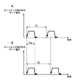
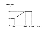
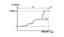
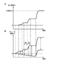
- FIG. 19A shows an example of a waveform diagram of the output current Io of the Cuk converter circuit at startup.
- the rising waveform of the output current Io is stepped by the stagnation period TA of the output current Io, and as a result, the output current Io becomes the rated value Ira (target Value) until it reaches (value) (the rise time of the output current Io) is delayed.
- a period in which the output current Io increases is referred to as an increase period TB.
- FIG. 19B shows a waveform diagram of the choke current Il flowing through the first inductor when the output current Io rises. Note that the solid line in FIG. 19B indicates the envelope of the peak value and the bottom value of the choke current Il that repeatedly increases and decreases.
- FIG. 20A shows an enlarged waveform diagram of the choke current Il during the stagnation period TA of the output current Io.
- FIG. 20B shows an enlarged waveform diagram of the choke current Il during the increase period TB of the output current Io.
- the choke current Il flowing through the first inductor increases during the on period Ton when the switching element is on, and decreases during the off period Toff when the switching element is off.
- the choke current Il is in the discontinuous mode.
- the switching element continues to be turned off even after the choke current Il is reduced to zero.
- the choke current Il freely oscillates (oscillates) with zero as a boundary, as shown in FIGS. 20A and 20B, due to the parasitic capacitance and the inductance of the first inductor. Oscillation of the choke current Il generates a timing at which the choke current Il is negative, that is, a current flows (reverses) from the coupling capacitor toward the first inductor.
- the first inductor stores positive energy when the choke current Il is positive. Therefore, as shown in FIG. 20B, when the switching element is turned on at a positive timing of the choke current Il, the value of the choke current Il at the next turn-off of the switching element becomes high, and is therefore accumulated in the first inductor. (Positive) energy also increases.
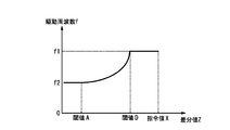
- a timing at which the choke current Il becomes zero is detected using a comparator, and the control is performed so that the choke current Il is in a critical mode by controlling the driving frequency f of the switching element (choke current Il).
- a method of turning on the switching element when Il becomes zero is conceivable. By this method, the reverse flow of the choke current Il does not occur, and the rise time of the output current Io can be greatly improved.
- the control since the control is complicated, when using an inexpensive microcomputer with low arithmetic processing performance, it is necessary to cut off other functions. In addition, there is a problem that the cost increases when the circuit is configured externally.
- a method of setting the drive frequency f (switching frequency) high can be considered.
- the drive frequency f switching frequency
- the present invention has been made in view of the above-described reasons, and an object of the present invention is to provide a lighting device capable of suppressing a decrease in circuit efficiency and shortening a rise time of an output current with an inexpensive configuration, and The object is to provide the used lighting fixtures and in-vehicle lighting fixtures.
- the lighting device of the present invention includes a power conversion circuit, a current detection unit, and a control unit.
- the power conversion circuit includes a first converter circuit having a first inductor and a second converter circuit having a second inductor.
- first converter circuit when a switching element is turned on, current flows from the DC power source to the first inductor through the switching element, whereby energy is accumulated in the first inductor, and the switching When the element is turned off, the energy stored in the first inductor is released, and charges are stored in the capacitor.
- the switching element when the switching element is turned on, current flows from the capacitor to the second inductor through the switching element, whereby energy is accumulated in the second inductor, When the switching element is turned off, the energy stored in the second inductor is released, thereby supplying a current to the light source.
- the current detection unit detects an output current supplied from the power conversion circuit to the light source.
- the control unit performs switching control of the switching element, and sets the duty ratio of the switching element based on a detection value of the output current detected by the current detection unit, whereby the output current is set to a target value.
- Feedback control is performed so that The control unit increases the drive current of the switching element at the time of starting up the output current that increases the output current from a zero state toward the target value, after increasing the output current to the target value.
- the output frequency is set higher than the drive frequency at the steady state.
- the control unit when the difference value obtained by subtracting the detection value from the target value is equal to or greater than a first threshold, the control unit sets the drive frequency to the first frequency, and the difference value is When it is less than the second threshold value that is equal to or less than the first threshold value, the drive frequency is set to a second frequency that is lower than the first frequency.
- the second threshold value is larger than a sum of a variation width of the output current and a ripple width of the output current in the steady state.
- the second threshold value is the same value as the first threshold value.
- the second threshold value is smaller than the first threshold value.
- the control unit changes the drive frequency from the first frequency to the second frequency as the difference value decreases. Decrease toward.
- the second threshold value is smaller than the first threshold value.
- the control unit changes the drive frequency from the first frequency to the second frequency as the difference value decreases. Decreasing in a linear function.
- the second threshold value is smaller than the first threshold value.
- the control unit is configured to reduce the drive frequency so that a slope for decreasing the drive frequency decreases as the difference value decreases. Is decreased from the first frequency toward the second frequency.
- the lighting device further includes a timer that measures an elapsed time after the control unit is activated.
- the controller sets the drive frequency to a first frequency when the elapsed time is less than a third threshold, and sets the drive frequency to the first frequency when the elapsed time is equal to or greater than the third threshold.
- a second frequency lower than the first frequency is set.
- the power conversion circuit includes a Cuk converter circuit or a modified Cuk converter circuit.
- the lighting fixture of the present invention includes a lighting device, a light source, a light source to which power is supplied from the lighting device, and a lighting device and a fixture main body to which the light source is attached.
- the lighting device includes a power conversion circuit, a current detection unit, and a control unit.
- the power conversion circuit includes a first converter circuit having a first inductor and a second converter circuit having a second inductor. In the first converter circuit, when a switching element is turned on, current flows from the DC power source to the first inductor through the switching element, whereby energy is accumulated in the first inductor, and the switching When the element is turned off, the energy stored in the first inductor is released, and charges are stored in the capacitor.
- the switching element when the switching element is turned on, current flows from the capacitor to the second inductor through the switching element, whereby energy is accumulated in the second inductor, When the switching element is turned off, the energy stored in the second inductor is released, thereby supplying a current to the light source.
- the current detection unit detects an output current supplied from the power conversion circuit to the light source.
- the control unit performs switching control of the switching element, and sets the duty ratio of the switching element based on a detection value of the output current detected by the current detection unit, whereby the output current is set to a target value.
- Feedback control is performed so that The control unit increases the drive current of the switching element at the time of starting up the output current that increases the output current from a zero state toward the target value, after increasing the output current to the target value.
- the output frequency is set higher than the drive frequency at the steady state.
- the on-vehicle lighting fixture of the present invention includes a lighting device, a light emitting element, a light source to which power is supplied from the lighting device, and a lamp provided on the vehicle to which the lighting device and the light source are attached.
- the lighting device includes a power conversion circuit, a current detection unit, and a control unit.
- the power conversion circuit includes a first converter circuit having a first inductor and a second converter circuit having a second inductor. In the first converter circuit, when a switching element is turned on, current flows from the DC power source to the first inductor through the switching element, whereby energy is accumulated in the first inductor, and the switching When the element is turned off, the energy stored in the first inductor is released, and charges are stored in the capacitor.
- the switching element when the switching element is turned on, current flows from the capacitor to the second inductor through the switching element, whereby energy is accumulated in the second inductor, When the switching element is turned off, the energy stored in the second inductor is released, thereby supplying a current to the light source.
- the current detection unit detects an output current supplied from the power conversion circuit to the light source.
- the control unit performs switching control of the switching element, and sets the duty ratio of the switching element based on a detection value of the output current detected by the current detection unit, whereby the output current is set to a target value.
- Feedback control is performed so that The control unit increases the drive current of the switching element at the time of starting up the output current that increases the output current from a zero state toward the target value, after increasing the output current to the target value.
- the output frequency is set higher than the drive frequency at the steady state.
- the drive frequency of the switching element at the time of rising of the output current is higher than the drive frequency at the time of steady output current, it is possible to suppress a decrease in circuit efficiency and reduce the output current with an inexpensive configuration. There is an effect that the start-up time can be shortened.
- FIG. 3A is a waveform diagram of the detection value of the above
- FIG. 10 is an operation flowchart of a control unit according to the third embodiment. It is a graph of the drive frequency with respect to a difference value same as the above. It is a wave form diagram of a detection value same as the above. 10 is an operation flowchart of a control unit according to the fourth embodiment. It is a graph of the drive frequency with respect to a difference value same as the above.
- FIG. 6 is a circuit configuration diagram of a lighting device according to a fifth embodiment. It is an operation
- FIG. 10 is a circuit configuration diagram of a lighting device including a modified Cuk converter circuit according to a sixth embodiment. FIG.
- FIG. 19A is a waveform diagram of an output current of a conventional lighting device with a fixed driving frequency
- FIG. 19B is a waveform diagram of a choke current of a conventional lighting device with a fixed driving frequency
- 20A and 20B are examples of enlarged waveform diagrams of the choke current in the stagnation period and the increase period of FIG. 19B, respectively.
- 21A to 21D are explanatory diagrams showing choke current waveforms when the driving frequency and the duty ratio are varied. It is typical sectional drawing of the lighting fixture of Embodiment 7.
- FIG. FIG. 10 is a schematic cross-sectional view of an in-vehicle lighting fixture of Embodiment 7. It is an external appearance perspective view of the vehicle using the same as the above.
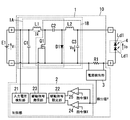
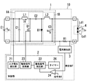
- FIG. 1 shows a circuit configuration diagram of a lighting device 10 of the present embodiment.
- the lighting device 10 of the present embodiment lights up a light source 4 including a plurality of LED elements Ld1 (light emitting elements) with a power conversion circuit 1, a control unit 2, and a current detection unit 3 as main components and a DC power source E1 as an input power source. It is something to be made.
- the power conversion circuit 1 includes a Cuk converter circuit that forms a first converter circuit 1A and a second converter circuit 1B.
- Power conversion circuit 1 includes capacitors C1, C2, C3, inductors L1, L2, switching element Q1, and diode D1.
- the first converter circuit 1A includes a capacitor C1 (first capacitor; smoothing capacitor), a capacitor C2 (second capacitor; coupling capacitor), an inductor L1 (first inductor), a switching element Q1, and a diode D1. It is composed of a boost chopper circuit.
- the capacitor C1 is connected between the output terminals of the DC power supply E1, and reduces noise of the input voltage Vi applied from the DC power supply E1.
- a series circuit of an inductor L1 and a switching element Q1 is connected in parallel with the capacitor C1. Specifically, the inductor L1 is connected to the positive side of the capacitor C1 (high voltage side of the DC power supply E1), and the switching element Q1 is connected to the negative side of the capacitor C1 (low voltage side of the DC power supply E1).
- the switching element Q1 is composed of an n-channel MOSFET and is switching-controlled by the control unit 2 described later.
- a series circuit of a capacitor C2 and a diode D1 is connected in parallel with the switching element Q1.
- a capacitor C2 is connected to a connection point between the inductor L1 and the switching element Q1
- a diode D1 is connected to a connection point between the capacitor C1 and the switching element Q1.
- the anode of the diode D1 is connected to the capacitor C2, and the cathode of the diode D1 is connected to the connection point between the capacitor C1 and the switching element Q1.
- the second converter circuit 1B includes a step-down chopper circuit including a capacitor C2, a capacitor C3 (third capacitor; output capacitor), an inductor L2 (second inductor), a switching element Q1, and a diode D1.
- a capacitor C2 third capacitor; output capacitor
- an inductor L2 second inductor
- the switching element Q1, and the diode D1 share the configuration of the first converter circuit 1A and the second converter circuit 1B.
- a series circuit of a capacitor C3 and an inductor L2 is connected in parallel with the diode D1 described above. Specifically, the inductor L2 is connected to the anode of the diode D1, and the capacitor C3 is connected to the cathode of the diode D1.
- the power conversion circuit 1 having the above-described configuration is configured such that the desired output voltage Vo obtained by converting the input voltage Vi applied from the DC power supply E1 is generated between both ends of the capacitor C3 by driving the switching element Q1 on and off. Generate.
- the power conversion circuit 1 generates an output voltage Vo in which the polarity of the input voltage Vi is inverted. Therefore, in the capacitor C3, the diode D1 side is a positive electrode and the inductor L2 side is a negative electrode.
- a light source 4 including a plurality of LED elements Ld1 is connected in parallel with the capacitor C3 via a resistor R1. Therefore, when the output voltage Vo of the power conversion circuit 1 is applied to the light source 4, the output current Io is supplied to the LED element Ld1, and the light source 4 is turned on.
- the light emitting element which comprises the light source 4 is not limited to LED element Ld1, and may be comprised by the organic EL element etc.
- the resistor R1 is a resistor for detecting the output current Io supplied to the light source 4.
- the current detector 3 detects the output current Io by detecting the voltage across the resistor R1, and outputs the detected value Y of the output current Io to the controller 2.
- the control unit 2 includes a microcomputer having an input voltage detection unit 21, a drive signal setting unit 22, a drive signal transmission unit 23, a comparator 24, and a subtraction unit 25. Then, the control unit 2 sets the duty ratio Don of the switching element Q1 based on the detection value Y, and performs feedback control so that the output current Io becomes the target value.
- the control unit 2 compares the command value X corresponding to the target value of the output current Io with the detected value Y. Then, the control unit 2 increases the duty ratio Don when the command value X is larger than the detection value Y, and decreases the duty ratio Don when the command value X is equal to or less than the detection value Y.
- the input voltage detector 21 is connected to the input end of the power conversion circuit 1 and detects the input voltage Vi applied to the power conversion circuit 1 (from the DC power supply E1). When the input voltage detection unit 21 detects that the input voltage Vi is a voltage value within a predetermined range, another function of the control unit 2 (a microcomputer constituting the control unit 2) is activated.
- the detection value Y is input to the inverting input terminal, and the command value X (corresponding to the target value) of the output current Io is input to the non-inverting input terminal.
- the comparator 24 outputs a positive voltage signal to the drive signal setting unit 22 when the command value X is larger than the detection value Y and a negative voltage signal when the command value X is equal to or less than the detection value Y. To do.
- the subtraction unit 25 receives the detection value Y at the inverting input terminal and the command value X at the non-inverting input terminal. Then, the subtraction unit 25 outputs a value obtained by subtracting the detection value Y from the command value X (hereinafter referred to as a difference value Z) to the drive signal setting unit 22.
- the drive signal setting unit 22 sets the duty ratio Don of the drive signal (signal supplied to the switching element Q1) based on the output of the comparator 24, and based on the output (difference value Z) of the subtraction unit 25.
- the drive frequency f of the drive signal is set.
- the drive signal transmission unit 23 drives the switching element Q1 on and off by outputting a drive signal to the switching element Q1.
- control unit 2 performs feedback control so that the output current Io becomes the target value by setting the duty ratio Don and the drive frequency f of the switching element Q1 based on the detection value Y.
- the operation of the first converter circuit 1A will be described.
- the switching element Q1 When the switching element Q1 is turned on, a current flows through the closed circuit of the DC power supply E1, the inductor L1, the switching element Q1, and the DC power supply E1, whereby energy is stored in the inductor L1.
- the switching element Q1 When the switching element Q1 is turned off, the energy stored in the inductor L1 is released.
- a current flows through the closed circuit of the inductor L1-capacitor C2-diode D1-DC power supply E1-inductor L1, so that charge is accumulated in the capacitor C2.
- the first converter circuit 1A generates a voltage boosted higher than the input voltage Vi of the DC power supply E1 between both ends of the capacitor C2 by driving the switching element Q1 on and off.
- the second converter circuit 1B operates using the capacitor C2 in which charges are accumulated by the first converter circuit 1A as a power source.
- the switching element Q1 When the switching element Q1 is turned on, the accumulated charge in the capacitor C2 is released. At this time, energy flows in the closed circuit of capacitor C2-switching element Q1-capacitor C3-inductor L2-capacitor C2, whereby energy is stored in inductor L2.
- the switching element Q1 is turned off, the energy accumulated in the inductor L2 is released.
- the second converter circuit 1B causes the voltage (output voltage Vo), which is stepped down lower than the voltage at both ends of the capacitor C2, to pass between the both ends of the capacitor C3 by driving the switching element Q1 on and off.
- the output voltage Vo generated across the capacitor C3 is higher or lower than the input voltage Vi of the DC power supply E1 is set by switching control (duty ratio Don, driving frequency f) of the switching element Q1 and circuit constants. Is done.
- the power conversion circuit 1 generates the output voltage Vo obtained by stepping up or down the input voltage Vi when the switching element Q ⁇ b> 1 is turned on / off, and applies the light source 4 to light the light source 4. .
- the switching element Q1 when the switching element Q1 is turned on, a current flows from the DC power source E1 to the inductor L1 (first inductor) via the switching element Q1, thereby storing energy in the inductor L1.
- the switching element Q1 When the switching element Q1 is turned off, the energy stored in the inductor L1 is released, so that charges are stored in the capacitor C2.
- the switching element Q1 when the switching element Q1 is turned on, the current flows from the capacitor C2 to the inductor L2 (second inductor) via the switching element Q1, so that energy is accumulated in the inductor L2.
- the switching element Q1 When the switching element Q1 is turned off, the energy stored in the inductor L2 is released, so that a current is supplied to the light source 4.
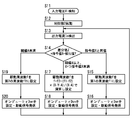
- the operation of the control unit 2 at the start-up of the lighting device 10 of the present embodiment that is, at the start-up of the output current Io that increases the output current Io from the zero state toward the target value (rated value Ira).
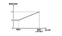
- the first threshold value to be compared with the difference value Z in order to set the driving frequency f to the first frequency f1, and the driving frequency to the second frequency f2 lower than the first frequency f1. Therefore, the second threshold value to be compared with the difference value Z is set to the same value (threshold value A).
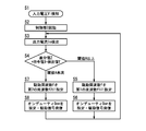
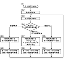
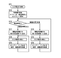
- step S1 when the DC power supply E1 is turned on, the control unit 2 is reset, and the input voltage detection unit 21 detects the voltage value of the input voltage Vi (step S1). And if the input voltage detection part 21 detects that the input voltage Vi is a voltage value of the predetermined range (operable voltage of the control part 2), the control part 2 will start (step S2).
- the current detection unit 3 detects the output current Io and outputs the detection value Y to the control unit 2 (step S3).
- the control unit 2 compares the command value X with the detection value Y using the comparator 24 and inputs a voltage signal corresponding to the comparison result to the drive signal setting unit 22.
- the control part 2 calculates the difference value Z by subtracting the detection value Y from the command value X using the subtraction part 25 (step S4).
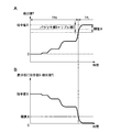
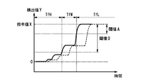
- FIG. 3A shows a waveform diagram of the detected value Y when the lighting device 10 is started.
- FIG. 3B shows a waveform diagram of the difference value Z when the lighting device 10 is started.
- the drive signal setting unit 22 sets the drive frequency f to the first frequency f1 (step S5).
- the drive signal setting unit 22 sets the duty set to the drive signal.
- the ratio Don is increased (step S6).
- the drive signal transmitter 23 outputs a drive signal in which the drive frequency f and the duty ratio Don are set to the gate of the switching element Q1, so that the switching element Q1 is driven on and off. Thereafter, the process returns to step S3.
- a period in which the first frequency f1 is set as the driving frequency f is referred to as a high frequency period TfH.
- the drive signal setting unit 22 sets the drive frequency f to a second frequency f2 lower than the first frequency f1 (step S7).
- the drive signal setting unit 22 sets the duty ratio Don set to the drive signal. increase.
- the drive signal setting unit 22 sets the duty ratio Don set to the drive signal. Reduce (step S8).
- the drive signal transmitter 23 outputs a drive signal in which the drive frequency f and the duty ratio Don are set to the gate of the switching element Q1, so that the switching element Q1 is driven on and off. Thereafter, the process returns to step S3.
- a period in which the second frequency f2 is set as the drive frequency f is referred to as a low frequency period TfL.
- the feedback control is performed so that the output current Io becomes the target value by repeatedly setting the drive frequency f and the duty ratio Don by the above control.
- the present embodiment is characterized in that the difference value Z (a value obtained by subtracting the detection value Y from the command value X) and the threshold A are compared, and the drive frequency f is switched based on the comparison result. .
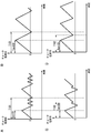
- FIGS. 21A to 21D show examples of waveform diagrams of the choke current Il flowing through the inductor L1 when the drive frequency f and the duty ratio Don of the switching element Q1 are changed.
- FIG. 21A is a waveform diagram of the choke current Il when the drive frequency f is low and the on period Ton is short.
- FIG. 21B is a waveform diagram of the choke current Il when the drive frequency f is low and the on period Ton is long.
- FIG. 21C is a waveform diagram of the choke current Il when the drive frequency f is high and the on period Ton is short.
- FIG. 21D is a waveform diagram of the choke current Il when the drive frequency f is high and the on period Ton is long.
- 21A and 21B is T101, and the switching period in FIGS. 21C and 21D is T102 ( ⁇ T101).
- 21A and 21C is Ton101
- the on period in FIGS. 21B and 21D is Ton102 (> Ton101).
- the ON period is increased from Ton101 (for example, 1.0 ⁇ s) to Ton102 (for example, 1.5 ⁇ s) (duty ratio Don is increased).
- Ton101 for example, 1.0 ⁇ s
- Ton102 for example, 1.5 ⁇ s
- the choke current Il becomes the discontinuous mode even if the on period is increased to Ton102.
- the drive frequency f is set high (switching cycle T102; see FIGS. 21C and 21D), as shown in FIG. 21D
- the choke current Il can be set to the continuous mode by increasing the ON period to Ton102. it can.
- the control unit 2 determines that the output current Io is being increased to increase the output current Io from the zero state toward the target value, and the drive frequency A high first frequency f1 is set to f (high frequency period TfH).
- the choke current Il flowing through the inductor L1 can be shifted from the discontinuous mode to the continuous mode with a small increase in the on period Ton (FIG. 21A to FIG. 21A). 21D).
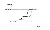
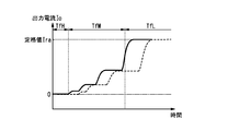
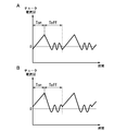
- FIG. 4 shows a waveform diagram of the output current Io when the output current Io is raised according to the present embodiment.
- the solid line is the waveform of the output current Io in the lighting device 10 of the present embodiment
- the broken line is the drive frequency f fixed at the second frequency f2 (the value of the drive frequency f in the steady state). It is a waveform of the output current Io in the case.
- the drive frequency f is set to a high first frequency f1, thereby shortening the rise time of the output current Io as shown in FIG. it can.
- the control unit 2 determines that the output current Io is relatively large and is close to the target value, and sets a low second frequency f2 to the drive frequency f (low frequency). Period TfL). Thereby, when the output current Io is steady, it is possible to suppress a decrease in circuit efficiency due to the switching loss of the switching element Q1. Further, the second frequency f2 set to the drive frequency f when the output current Io is steady is set to a value suitable for rated lighting of the light source 4. Therefore, the light source 4 can be stably lit at the rated output current Io.
- the threshold A is set to a value larger than the sum of the variation width B of the output current Io in the decreasing direction and the ripple width C of the output current Io in the decreasing direction with respect to the target value.
- the sum of the variation width B and the ripple width C is a width in which the detected value Y at the steady state of the output current Io can vary (decrease).
- the difference value Z becomes equal to or greater than the threshold value A when the output current Io is steady, and the drive frequency f is increased. Fluctuation (change from the second frequency f2 to the first frequency f1) is prevented. Thereby, when the light source 4 is rated on, stable lighting control can be performed, and the lighting state of the light source 4 can be stabilized.
- the power conversion circuit 1 that supplies the output current Io to the light source 4 is constituted by a Cuk converter circuit. Since the Cuk converter circuit is composed of an inexpensive choke coil without using an expensive large transformer, the cost can be reduced and the lighting device 10 can be configured at low cost. Further, the Cuk converter circuit has an advantage that the ripple of the input / output current is stabilized.
- control method (the method of changing the drive frequency f in accordance with the comparison result between the difference value Z and the threshold value A) is not only when the output current Io is raised when the lighting device 10 is started, but also the output current Io. This is also effective when returning to the target value when the value temporarily decreases.
- the drive frequency f is set to the first frequency f1 (> the second frequency f2 that is the steady-state drive frequency f). Therefore, the output current Io can be returned to the target value in a short time.
- the drive frequency f is set based only on the command value X and the detection value Y, it is not necessary to design a margin based on fluctuations in the input voltage Vi and the light source 4 (load).
- the control method is not only a DC lighting method (see FIG. 4) for supplying a direct current to the light source 4, but also a pulse (PWM) lighting method (see FIG. 5) for intermittently supplying a direct current to the light source 4. Is also effective, and the same effect as described above can be obtained.
- the comparator 24 may be configured by a subtraction circuit that outputs a difference value Z obtained by subtracting the detection value Y from the command value X.
- the drive signal setting unit 22 compares the difference value Z with a preset threshold value (for example, “zero”), and sets the duty ratio Don of the drive signal based on the comparison result.
- the lighting device 10 of the present embodiment is characterized in that when the driving frequency f is switched from the first frequency f1 to the second frequency f2, the fluctuation of the driving frequency f is controlled gently.
- the other control and lighting device 10 configurations are the same as those in the first embodiment, and a description thereof will be omitted.
- the drive frequency f when the difference value Z is greater than or equal to the threshold A, the drive frequency f is set to the first frequency f1, and when the difference value Z is less than the threshold A, the drive frequency f is set to the second frequency f2. It was set (see Fig. 2). That is, the first threshold value and the second threshold value are set to the same value. Therefore, the drive frequency f changes greatly with the threshold A as a boundary.
- FIG. 6A shows a waveform diagram of the gate voltage of the switching element Q1 when the drive frequency f is the first frequency f1.
- FIG. 6B shows a waveform diagram of the gate voltage of the switching element Q1 when the drive frequency f is the second frequency f2.
- 6A and 6B the on period of the switching element Q1 is Ton.
- the duty ratio Don1 in FIG. 6A is the ON period Ton / drive period T1.
- the duty ratio Don2 in FIG. 6B is the ON period Ton / drive cycle T2. Since the drive cycle is T1 ⁇ T2, the duty ratio Don1> the duty ratio Don2. Therefore, at the timing when the drive frequency f is switched from the first frequency f1 to the second frequency f2, the duty ratio Don is reduced and the output current Io is greatly reduced. On the other hand, at the timing when the drive frequency f is switched from the second frequency f2 to the first frequency f1, the duty ratio Don increases, the output current Io increases, and an overcurrent is generated. In particular, flickering of the light source 4 may occur when the drive frequency f is repeatedly increased and decreased during the steady state of the output current Io.
- step S11 when the DC power supply E1 is turned on, the control unit 2 is reset, and the input voltage detection unit 21 detects the voltage value of the input voltage Vi (step S11). Then, when the input voltage detection unit 21 detects that the input voltage Vi is a voltage value within a predetermined range (operational voltage of the control unit 2), the control unit 2 is activated (step S12).
- the current detection unit 3 detects the output current Io and outputs the detection value Y to the control unit 2 (step S13).
- the control unit 2 compares the command value X with the detection value Y using the comparator 24 and inputs a voltage signal corresponding to the comparison result to the drive signal setting unit 22.
- the control part 2 calculates the difference value Z by subtracting the detection value Y from the command value X using the subtraction part 25 (step S14).
- the drive signal setting unit 22 compares the difference value Z input from the subtraction unit 25 with the preset threshold value A (“second threshold value”) and threshold value F (“first threshold value”). Based on the voltage signal input from the comparator 24, the drive signal (the drive frequency f of the switching element Q1, the duty ratio Don) is set.
- the threshold value F is set to a value equal to the command value X as shown in FIG.
- FIG. 8 shows a graph of the driving frequency f with respect to the difference value Z.
- FIG. 9 shows a waveform diagram when the output current Io rises in this embodiment.
- the solid line is the waveform of the output current Io in the lighting device 10 of the present embodiment
- the broken line is the waveform of the output current Io when the drive frequency f is fixed at the second frequency f2.
- the drive signal setting unit 22 sets the drive frequency f to the first value. 1 is set to a frequency f1 (step S15).
- the drive signal setting unit 22 sets the duty set to the drive signal.
- the ratio Don is increased (step S16).
- the drive signal transmitter 23 outputs a drive signal in which the drive frequency f and the duty ratio Don are set to the gate of the switching element Q1, so that the switching element Q1 is driven on and off. Thereafter, the process returns to step S13.
- the drive signal setting unit 22 calculates the drive frequency f by the following formula (1).
- a value is set (step S17).
- the drive signal setting unit 22 sets the drive frequency f as the difference value Z decreases.
- the frequency is set so as to decrease from the first frequency f1 toward the second frequency f2.
- the drive signal setting unit 22 changes the drive frequency f from the first frequency f1 to the second frequency as the difference value Z decreases. It is set so as to decrease linearly toward f2.
- the drive signal setting unit 22 sets the duty set to the drive signal.
- the ratio Don is increased (step S18).
- the drive signal transmission unit 23 outputs the drive signal in which the drive frequency f and the duty ratio Don are set to the gate of the switching element Q1, thereby driving the switching element Q1 on and off. Thereafter, the process returns to step S13.
- a period during which the drive frequency f is decreased from the first frequency f1 toward the second frequency f2 is referred to as a frequency decrease period TfM.
- the drive signal setting unit 22 sets the drive frequency f to the second frequency f2 (step S19).
- the drive signal setting unit 22 sets the duty ratio Don set to the drive signal. increase.
- the drive signal setting unit 22 sets the duty ratio Don set to the drive signal. Reduce (step S20). Then, the drive signal transmission unit 23 outputs the drive signal in which the drive frequency f and the duty ratio Don are set to the gate of the switching element Q1, thereby driving the switching element Q1 on and off. Thereafter, the process returns to step S13.
- the feedback control is performed so that the output current Io becomes the target value by repeatedly setting the drive frequency f and the duty ratio Don by the above control.
- the drive frequency f increases from the first frequency f1 to the second frequency as the difference value Z decreases. Decreases linearly (linearly) toward the frequency f2. Therefore, in the present embodiment, the drive frequency f is controlled so as to vary gently without suddenly changing from the first frequency f1 to the second frequency f2, so that the output current Io varies due to the sudden change in the drive frequency f. Is suppressed. Thereby, the flicker of the light source 4 at the time of the steady state of the output current Io can be suppressed.
- the drive frequency f at the time of rising of the output current Io is higher than the drive frequency f (second frequency f2) at the steady time of the output current Io, as shown in FIG.
- the rise time of the output current Io can be shortened compared with the case where the frequency f2 is fixed.
- the lighting device 10 according to the present embodiment is characterized in that the period during which the drive frequency f is set to the first frequency f1 (high-frequency period TfH) is expanded as compared with the second embodiment.
- the other control and lighting device 10 configurations are the same as those in the second embodiment, and a description thereof will be omitted.
- the period for setting the drive frequency f to the first frequency f1 (the high frequency period TfH) is expanded to achieve both shortening the rise time of the output current Io and suppressing flickering of the light source 4. .
- the operation of the control unit 2 at the time of starting the lighting device 10 of the present embodiment will be described with reference to the flowchart shown in FIG.
- step S31 when the DC power supply E1 is turned on, the control unit 2 is reset, and the input voltage detection unit 21 detects the voltage value of the input voltage Vi (step S31). Then, when the input voltage detection unit 21 detects that the input voltage Vi is a voltage value within a predetermined range (operational voltage of the control unit 2), the control unit 2 is activated (step S32).
- the current detection unit 3 detects the output current Io and outputs the detection value Y to the control unit 2 (step S33).
- the control unit 2 compares the command value X with the detection value Y using the comparator 24 and inputs a voltage signal corresponding to the comparison result to the drive signal setting unit 22.
- the control part 2 calculates the difference value Z by subtracting the detection value Y from the command value X using the subtraction part 25 (step S34).
- the drive signal setting unit 22 compares the difference value Z input from the subtraction unit 25 with a preset threshold A (“second threshold”) and threshold D (“first threshold”). Based on the voltage signal input from the comparator 24, the drive signal (the drive frequency f of the switching element Q1, the duty ratio Don) is set.
- the threshold value D is set to a value larger than the threshold value A and smaller than the command value X.
- FIG. 11 shows a graph of the driving frequency f with respect to the difference value Z.
- FIG. 12 shows a waveform diagram of the detected value Y when the lighting device 10 is started. Note that the solid line in FIG. 12 is the waveform of the detection value Y of the present embodiment, and the broken line is the waveform of the detection value Y of the second embodiment.
- the drive signal setting unit 22 sets the drive frequency f to the first frequency f1 (step S35).
- the drive signal setting unit 22 sets the duty set to the drive signal.
- the ratio Don is increased (step S36).
- the drive signal transmitter 23 outputs a drive signal in which the drive frequency f and the duty ratio Don are set to the gate of the switching element Q1, so that the switching element Q1 is driven on and off. Thereafter, the process returns to step S33.
- the drive signal setting unit 22 sets the drive frequency f to a value calculated by the following equation (2) (step) S37).
- the drive signal setting unit 22 sets the drive frequency f to the first value as the difference value Z decreases.
- the frequency f1 is set so as to decrease from the frequency f1 toward the second frequency f2.
- the drive signal setting unit 22 sets the drive frequency f to the first frequency f1 as the difference value Z decreases. Is set so as to decrease linearly toward the second frequency f2.
- the drive signal setting unit 22 sets the duty set to the drive signal.
- the ratio Don is increased (step S38).
- the drive signal transmission unit 23 outputs the drive signal in which the drive frequency f and the duty ratio Don are set to the gate of the switching element Q1, thereby driving the switching element Q1 on and off. Thereafter, the process returns to step S33.
- the drive signal setting unit 22 sets the drive frequency f to the second frequency f2 (step S39).
- the drive signal setting unit 22 sets the duty ratio Don set to the drive signal. increase.
- the drive signal setting unit 22 sets the duty ratio Don set to the drive signal. Reduce (step S40). Then, the drive signal transmission unit 23 outputs the drive signal in which the drive frequency f and the duty ratio Don are set to the gate of the switching element Q1, thereby driving the switching element Q1 on and off. Thereafter, the process returns to step S33.
- the feedback control is performed so that the output current Io becomes the target value by repeatedly setting the drive frequency f and the duty ratio Don by the above control.
- step S34 to S40 By performing the above control (steps S34 to S40), as shown in FIG. 11, when the difference value Z is not less than the threshold value D, the drive frequency f is set to the upper limit value. Then, as the difference value Z approaches the threshold value A from the threshold value D, the drive frequency f is set so as to approach the second frequency f2 from the first frequency f1.
- the output is higher than that in the second embodiment as shown in FIG.
- the effect of shortening the rise time of the current Io is increased.
- the drive frequency f is set so as to decrease linearly from the first frequency f1 toward the second frequency f2 (frequency decrease period TfM), flickering of the light source 4 due to a sudden change in the drive frequency f. Can also be suppressed.
- a high frequency period TfH in which the driving frequency f is set to the first frequency f1 and a gradient in which the driving frequency f decreases from the first frequency f1 toward the second frequency f2.
- the rise time of the output current Io and the fluctuation of the output current Io due to the fluctuation of the drive frequency f can be easily adjusted.
- the lighting device 10 of the present embodiment is characterized in that when the difference value Z is greater than or equal to the threshold value A and less than the threshold value D, the drive frequency f is reduced in a quadratic function (curved).
- the other control and lighting device 10 configurations are the same as those in the third embodiment, and a description thereof will be omitted.
- the drive frequency f is decreased as the difference value Z decreases. Add control to reduce the tilt.
- the operation of the control unit 2 at the time of starting the lighting device 10 of the present embodiment will be described with reference to the flowchart shown in FIG.
- step S51 when the DC power supply E1 is turned on, the control unit 2 is reset, and the input voltage detection unit 21 detects the voltage value of the input voltage Vi (step S51). Then, when the input voltage detection unit 21 detects that the input voltage Vi is a voltage value within a predetermined range (operational voltage of the control unit 2), the control unit 2 is activated (step S52).
- the current detection unit 3 detects the output current Io and outputs the detection value Y to the control unit 2 (step S53).
- the control unit 2 compares the command value X with the detection value Y using the comparator 24 and inputs a voltage signal corresponding to the comparison result to the drive signal setting unit 22.
- the control unit 2 calculates a difference value Z by subtracting the detection value Y from the command value X using the subtraction unit 25 (step S54).
- the drive signal setting unit 22 compares the difference value Z input from the subtraction unit 25 with a preset threshold A (“second threshold”) and threshold D (“first threshold”). Based on the voltage signal input from the comparator 24, the drive signal (the drive frequency f of the switching element Q1, the duty ratio Don) is set.
- FIG. 14 shows a graph of the drive frequency f with respect to the difference value Z.
- the drive signal setting unit 22 sets the drive frequency f to the first frequency f1 (step S55).
- the drive signal setting unit 22 sets the duty set to the drive signal.
- the ratio Don is increased (step S56).
- the drive signal transmitter 23 outputs a drive signal in which the drive frequency f and the duty ratio Don are set to the gate of the switching element Q1, so that the switching element Q1 is driven on and off. Thereafter, the process returns to step S53.
- the drive signal setting unit 22 sets the drive frequency f to a value calculated by the following equation (3) (step) S57).
- the drive signal setting unit 22 sets the drive frequency f to the first value as the difference value Z decreases.
- the frequency f1 is set so as to decrease from the frequency f1 toward the second frequency f2.
- the drive signal setting unit 22 decreases the drive frequency f from the first frequency f1 toward the second frequency f2 as the difference value Z decreases.
- the drive frequency f is set as follows.
- the drive signal setting unit 22 sets the drive frequency f so that the gradient that decreases the drive frequency f decreases as the difference value Z approaches the threshold value A from the threshold value D.
- the drive signal setting unit 22 sets the duty set to the drive signal.
- the ratio Don is increased (step S58).
- the drive signal transmission unit 23 outputs the drive signal in which the drive frequency f and the duty ratio Don are set to the gate of the switching element Q1, thereby driving the switching element Q1 on and off. Thereafter, the process returns to step S53.
- the drive signal setting unit 22 sets the drive frequency f to the second frequency f2 (step S59).
- the drive signal setting unit 22 sets the duty ratio Don set to the drive signal. increase.
- the drive signal setting unit 22 sets the duty ratio Don set to the drive signal. Reduce (step S60). Then, the drive signal transmission unit 23 outputs the drive signal in which the drive frequency f and the duty ratio Don are set to the gate of the switching element Q1, thereby driving the switching element Q1 on and off. Thereafter, the process returns to step S53.
- the feedback control is performed so that the output current Io becomes the target value by repeatedly setting the drive frequency f and the duty ratio Don by the above control.
- the drive frequency f decreases from the first frequency f1 toward the second frequency f2 as the difference value Z decreases. .
- the gradient for decreasing the drive frequency f decreases, that is, the amount of change in the drive frequency f decreases.
- FIG. 15 shows a circuit configuration diagram of the lighting device 10 of the present embodiment.
- the lighting device 10 of the present embodiment is characterized in that the drive frequency f is switched based on the elapsed time ts after the control unit 2 is activated.
- the control unit 2 of this embodiment does not include the subtraction unit 25 included in the control unit 2 of the first to fourth embodiments, but includes a timer 26 instead. Since other configurations are the same as those of the first to fourth embodiments, the same reference numerals as those of the first embodiment are given and description thereof is omitted.
- the timer 26 measures an elapsed time ts after the input voltage Vi is applied to the lighting device 10 and the control unit 2 is activated. Then, the timer 26 outputs the measured elapsed time ts to the drive signal setting unit 22.
- step S71 when the DC power supply E1 is turned on, the control unit 2 is reset, and the input voltage detection unit 21 detects the voltage value of the input voltage Vi (step S71). Then, when the input voltage detection unit 21 detects that the input voltage Vi is a voltage value within a predetermined range (operational voltage of the control unit 2), the control unit 2 is activated (step S72). Then, the timer 26 starts measuring the elapsed time ts starting from the time when the control unit 2 is activated.
- the drive signal setting unit 22 compares the elapsed time ts with a preset threshold time E (“third threshold”), and sets the drive frequency f based on the comparison result (step S73).
- FIG. 17 shows a waveform diagram of the output current Io when the lighting device 10 is started.
- the drive signal setting unit 22 sets the drive frequency f to the first frequency f1 (step S74).
- the threshold time E is required for the output current Io to reach the rated value Ira (target value) after the control unit 2 is activated when the drive frequency f is set to the first frequency f1. It is set over time.
- the current detection unit 3 detects the output current Io and outputs the detection value Y to the control unit 2 (step S75).
- the control unit 2 uses the comparator 24 to compare the command value X and the detection value Y, and inputs a voltage signal corresponding to the comparison result to the drive signal setting unit 22.
- the drive signal setting unit 22 sets the duty ratio Don of the drive signal based on the voltage signal input from the comparator 24.
- the command value X is larger than the detected value Y (the voltage signal of the comparator 24 is positive), that is, when the output current Io is smaller than the target value
- the drive signal setting unit 22 increases the duty ratio Don set for the drive signal. .
- step S76 the drive signal transmitter 23 outputs a drive signal in which the drive frequency f and the duty ratio Don are set to the gate of the switching element Q1, so that the switching element Q1 is driven on and off. Thereafter, the process returns to step S73.
- the drive signal setting unit 22 sets the drive frequency f to the second frequency f2 (step S77).
- the current detection unit 3 detects the output current Io and outputs the detection value Y to the control unit 2 (step S78).
- the control unit 2 uses the comparator 24 to compare the command value X and the detection value Y, and inputs a voltage signal corresponding to the comparison result to the drive signal setting unit 22. Then, the drive signal setting unit 22 sets the duty ratio Don of the drive signal based on the voltage signal input from the comparator 24.
- step S79 The drive signal transmitter 23 outputs a drive signal in which the drive frequency f and the duty ratio Don are set to the gate of the switching element Q1, so that the switching element Q1 is driven on and off. Thereafter, the process returns to step S78.
- the elapsed time ts and the threshold time E are compared to determine whether the output current Io is rising or when the output current Io is steady. To do.
- the drive signal setting unit 22 determines that the output current Io is rising and sets the drive frequency f to the first frequency f1. Thereby, the rise time of the output current Io can be shortened.
- the drive signal setting unit 22 determines that the output current Io is steady and sets the drive frequency f to the second frequency f2. Thereby, the fall of the circuit efficiency by the switching loss of the switching element Q1 can be suppressed.
- the rise time of the output current Io varies due to various factors such as fluctuations in the input voltage Vi and load (light source 4) and circuit element variations. Therefore, it is desirable to set the threshold time E with a margin in consideration of variations in the rise time of the output current Io (see FIG. 17).
- the time when the control unit 2 that is the starting point of the measurement of the elapsed time ts is the time when the input voltage Vi is in a predetermined range (operable voltage of the control unit 2). It is not limited to.
- the measurement of the elapsed time ts is started with the time when the control unit 2 starts the switching control of the switching element Q1 or the time when the supply of the output current Io is started to the light source 4 being the time when the control unit 2 is activated. May be.
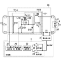
- the lighting device 20 of the present embodiment is characterized in that the power conversion circuit 101 is configured by a modified Cuk converter circuit.
- the lighting device 20 of the present embodiment will be described with reference to FIG.
- symbol is attached
- the lighting device 20 is configured to light a light source 4 including a plurality of LED elements Ld1 with a power conversion circuit 101, a control unit 2, and a current detection unit 3 as main components and a DC power supply E1 as an input power supply. .
- the power conversion circuit 101 includes a modified Cuk converter circuit that forms a first converter circuit 101A and a second converter circuit 101B.
- the power conversion circuit 101 includes capacitors C101, C102, C103, a transformer Tr101, an inductor L103, a switching element Q101, and a diode D101.
- Transformer Tr101 includes a primary winding L101 and a secondary winding L102.
- the first converter circuit 101A includes a capacitor C101 (first capacitor; smoothing capacitor), a capacitor C102 (second capacitor; coupling capacitor), a primary winding L101 and a secondary winding L102 (first inductor) of the transformer Tr101. ), A step-up chopper circuit including a switching element Q101 and a diode D101.
- the capacitor C101 is connected between the output terminals of the DC power supply E1, and reduces noise of the input voltage Vi applied from the DC power supply E1.
- a series circuit of the primary winding L101 of the transformer Tr101 and the switching element Q101 is connected in parallel with the capacitor C101.
- the primary winding L101 is connected to the positive side of the capacitor C101 (high voltage side of the DC power supply E1), and the switching element Q101 is connected to the negative side of the capacitor C101 (low voltage side of the DC power supply E1).
- the switching element Q101 is composed of an n-channel MOSFET and is switching-controlled by the control unit 2. Further, a series circuit of a capacitor C102, a secondary winding L102 of a transformer Tr101, and a diode D101 is connected in parallel with the switching element Q101.
- the capacitor C102 is connected to the connection point between the primary winding L101 and the switching element Q101, and the diode D101 is connected to the connection point between the negative electrode side of the capacitor C101 (the low voltage side of the DC power supply E1) and the switching element Q101. ing.
- the anode of the diode D101 is connected to the secondary winding L102, and the cathode of the diode D101 is connected to the connection point between the capacitor C101 and the switching element Q101.
- the second converter circuit 101B includes a secondary winding L102 of the transformer Tr101, a capacitor C102, a capacitor C103 (third capacitor; output capacitor), an inductor L103 (second inductor), a switching element Q101, and a diode D101. Consists of a step-down chopper circuit. Note that the secondary winding L102, the capacitor C102, the switching element Q101, and the diode D101 of the transformer Tr101 share the configuration of the first converter circuit 101A and the second converter circuit 101B. A series circuit of a capacitor C103 and an inductor L103 is connected in parallel with the series circuit of the secondary winding L102 and the diode D101 described above. Specifically, the cathode of the diode D101 is connected to the capacitor C103, and the inductor L103 is connected to the connection point between the secondary winding L102 and the capacitor C102.
- the power conversion circuit 101 having the above-described configuration causes the switching element Q101 to be turned on / off so that a desired output voltage Vo obtained by converting the input voltage Vi applied from the DC power source E1 is applied between both ends of the capacitor C103. Generate.
- the power conversion circuit 101 generates an output voltage Vo in which the polarity of the input voltage Vi is inverted. Therefore, the diode D101 side of the capacitor C103 is a positive electrode, and the inductor L103 side is a negative electrode.
- a light source 4 including a plurality of LED elements Ld1 is connected in parallel with the capacitor C103 via a resistor R1. Therefore, when the output voltage Vo of the power conversion circuit 101 is applied to the light source 4, the output current Io is supplied to each LED element Ld1, and the LED element Ld is turned on.
- the switching element Q101 when the switching element Q101 is turned on, a current flows through a closed circuit of the DC power supply E1-primary winding L101-switching element Q101-DC power supply E1, whereby energy is accumulated in the transformer Tr101.
- the switching element Q101 When the switching element Q101 is turned off, the energy stored in the transformer Tr101 is released. At this time, electric current flows in the closed circuit of secondary winding L102-diode D101-DC power supply E1-primary winding L101-capacitor C102-secondary winding L102, so that charge is accumulated in capacitor C102.
- the switching element Q101 is turned on / off, whereby the voltage across the capacitor C102 is boosted to a voltage higher than the input voltage Vi of the DC power supply E1.
- the power conversion circuit 101 generates the output voltage Vo obtained by stepping up or down the input voltage Vi when the switching element Q101 is turned on / off, and applies the light source 4 to light the light source 4. .
- the switching element Q101 when the switching element Q101 is turned on, a current flows from the DC power supply E1 to the primary winding L101 (first inductor) of the transformer Tr101 via the switching element Q101.
- the energy is stored in the transformer Tr101, and when the switching element Q101 is turned off, the energy stored in the transformer Tr101 is released, so that charges are stored in the capacitor C102.
- the switching element Q101 when the switching element Q101 is turned on, a current flows from the capacitor C102 to the inductor L103 (second inductor) via the switching element Q101, whereby energy is accumulated in the inductor L103.
- the switching element Q101 is turned off, the energy stored in the inductor L103 is released, so that a current is supplied to the light source 4.
- the same effect as that of the lighting device 10 of the first embodiment can be obtained by the lighting device 20 of the present embodiment.
- the energy of the power source can be effectively utilized even when the switching element Q101 is turned off, and the transformer can be downsized as compared with the flyback converter circuit. There is an advantage.
- the power conversion circuit 101 of the present embodiment may be applied to the lighting device 10 of the second to fifth embodiments.
- FIG. 22 is a schematic cross-sectional view of the lighting fixture of the present embodiment.
- FIG. 23 is a schematic cross-sectional view of the in-vehicle lighting device of this embodiment, and
- FIG. 24 is an external view of the vehicle of this embodiment provided with this in-vehicle lighting device.
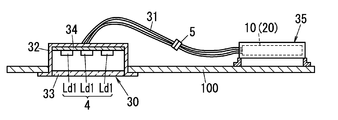
- a lighting fixture 30 shown in FIG. 22 includes the lighting device 10 (or 20) described in any of the first to sixth embodiments and the LED element (light emitting element) Ld1, and power is supplied from the lighting device 10 (20).
- the light source 4 to be supplied, and the lighting device 10 (20) and the instrument bodies 32 and 35 to which the light source 4 is attached are provided.
- the lighting fixture 30 houses the lighting device 10 (20) in a case 35 different from the fixture housing 32 of the light source 4, and the light source 4 (LED element Ld 1) via the lead wire 31. Are connected to the lighting device 10 (20). Thereby, the lighting fixture 30 can reduce the thickness of the light source 4, and the degree of freedom of the installation location of the lighting device 10 (20) increases.
- the instrument housing 32 is a metal bottomed cylindrical housing having an open lower surface, and the open surface (lower surface) is covered with a light diffusion plate 33.
- the light source 4 includes a plurality of (here, three) LED elements Ld1 mounted on one surface (lower surface) of the substrate 34, and is disposed in the appliance housing 32 in a direction facing the light diffusion plate 33.
- the appliance housing 32 is embedded in the ceiling 100, and is connected to the lighting device 10 (20) disposed on the back of the ceiling via the lead wire 31 and the connector 5.
- the lighting fixture 30 is not limited to a separate power source configuration in which the lighting device 10 (20) is housed in a separate case from the light source 4, and the lighting device 10 (20) is mounted in the same housing as the light source 4.
- a housed power source integrated configuration may be used.
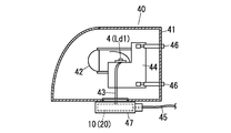
- the headlamp 40 includes the lighting device 10 (or 20) described in any of the first to sixth embodiments and the LED element (light emitting element) Ld1, and is supplied with electric power from the lighting device 10 (20).
- the light source 4 the lighting device 10 (20), a lamp 41 to which the light source 4 is attached, and an optical unit 42 disposed in front of the light source 4 (on the left side in FIG. 23) inside the lamp 41 as main components. ing.
- the lighting device 10 (20) is housed in a housing 47, and the housing 47 is attached to the lamp 41.
- the lighting device 10 (20) and the light source 4 are electrically connected by an output line 43, and lighting power is supplied to the light source 4 through the output line 43.
- a heat radiating plate 44 is attached to the light source 4, and heat generated by the light source 4 is radiated to the outside by the heat radiating plate 44.
- the optical unit 42 is composed of a lens, and controls the light distribution of the light emitted from the light source 4.
- the lighting device 10 (20) is attached to the lower surface of the lamp 41, and is supplied with power from a vehicle-mounted battery (not shown) as a DC power supply E1 provided in the vehicle via a power line 45.
- the light source unit including the light source 4, the optical unit 42, the heat radiating plate 44, and the like is attached to the lamp 41 by a fixture 46.
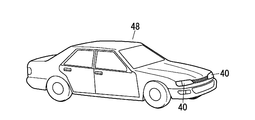
- FIG. 24 is an external perspective view of a vehicle 48 on which a pair of headlamps 40 described above are mounted on the left and right.
- the in-vehicle lighting fixture is not limited to the headlamp 40, and may be a direction indicator or a taillight of the vehicle 48.
Landscapes
- Engineering & Computer Science (AREA)
- Power Engineering (AREA)
- Circuit Arrangement For Electric Light Sources In General (AREA)
- Dc-Dc Converters (AREA)
Abstract
A lighting apparatus (10) is provided with: a power conversion circuit (1), which is configured from a Cuk converter circuit that forms first and second converter circuits (1A, 1B), and which supplies an output current (Io) to a light source (4) when a switching element (Q1) is on/off driven; a current detecting unit (3) that detects the output current (Io); and a control unit (2), which performs feedback control such that the output current (Io) is at a target value by setting a duty ratio of the switching element (Q1) on the basis of a detection value (Y) of the output current (Io). The control unit (2) sets a drive frequency (f) of the switching element (Q1) higher for the startup time of the output current (Io) than a drive frequency (f) at which the output current (Io) is in a steady state.
Description
本発明は、点灯装置および、これを用いた照明器具,車載用照明器具に関するものである。
The present invention relates to a lighting device, a lighting fixture using the lighting device, and an in-vehicle lighting fixture.
近年、LEDの高効率化,高輝度化に伴い、ダウンライト照明,直管型照明,および車両用前照灯などの光源としてLEDの需要が高まってきた。そして、このLEDの急速な普及に伴い、LEDを点灯させる点灯装置の開発が急務とされている。
In recent years, with the increase in efficiency and brightness of LEDs, the demand for LEDs as light sources for downlight illumination, straight tube illumination, and vehicle headlamps has increased. With the rapid spread of LEDs, there is an urgent need to develop a lighting device that lights the LEDs.
また、車載業界においてもLED光源を用いた前照灯の点灯装置の開発が盛んに行われており、中でも低コスト化が重要な課題にあげられている。点灯装置の低コスト化のためには、高価な大型トランスを用いたDC-DCコンバータ方式や、高ビットマイコンを用いた制御を避け、安価なコイル・小型トランスや低ビットマイコンを採用することが手段の一つといえる。
Also, in the in-vehicle industry, development of lighting devices for headlamps using LED light sources has been actively conducted, and in particular, cost reduction has been raised as an important issue. In order to reduce the cost of the lighting device, it is necessary to avoid the DC-DC converter method using an expensive large transformer and the control using a high bit microcomputer, and to adopt an inexpensive coil / small transformer or a low bit microcomputer. It can be said that it is one of the means.
そこで、トランスを使用せずチョークコイルで構成され、入出力電流のリプルが安定するCukコンバータ回路が注目されている(例えば、日本国特許出願公開2005-224094号公報参照)。
Therefore, a Cuk converter circuit, which is composed of a choke coil without using a transformer and has stable input / output current ripple, has been attracting attention (see, for example, Japanese Patent Application Publication No. 2005-224094).
Cukコンバータ回路は、第1のインダクタと、第2のインダクタと、第1のインダクタと第2のインダクタとの間に接続されたコンデンサ(以降、結合コンデンサと称する)と、スイッチング素子とを含む。Cukコンバータ回路では、スイッチング素子のスイッチング動作に応じて、電源→第1のインダクタ→結合コンデンサ→第2のインダクタの順にエネルギーが移動し、第2のインダクタに蓄積したエネルギーを外部に放出する。
The Cuk converter circuit includes a first inductor, a second inductor, a capacitor (hereinafter, referred to as a coupling capacitor) connected between the first inductor and the second inductor, and a switching element. In the Cuk converter circuit, energy moves in the order of power source → first inductor → coupling capacitor → second inductor according to the switching operation of the switching element, and the energy stored in the second inductor is released to the outside.
上記のCukコンバータ回路からなる電力変換回路を用い、さらに、演算速度が遅いが安価な低ビットマイコンからなる制御部を採用することで、点灯装置のコストを削減することができる。
The cost of the lighting device can be reduced by using the power conversion circuit composed of the above-described Cuk converter circuit and further adopting a control unit composed of an inexpensive low-bit microcomputer with a slow calculation speed.
しかしながら、上述したCukコンバータ回路と、演算速度の遅い低ビットマイコンとを組み合わせた場合、以下の問題が発生する。
However, when the above-described Cuk converter circuit is combined with a low-bit microcomputer having a low calculation speed, the following problem occurs.
光源を消灯状態から定格点灯させる場合には、制御部は、フィードバック制御によってスイッチング素子のデューティ比を徐々に増加させることで、電力変換回路の出力電流を目標値まで増加させる。
In the case where the light source is rated-lit from the extinguished state, the control unit gradually increases the duty ratio of the switching element by feedback control, thereby increasing the output current of the power conversion circuit to the target value.
しかし、演算速度が遅い低ビットマイコンで制御部を構成した場合、出力電流のフィードバック制御(デューティ比の更新)が遅くなる。そのため、出力電流をゼロの状態から目標値に向かって増加させる出力電流の立ち上げ時において、出力電流のオーバーシュートを抑制するために、デューティ比の増加度合いを緩やかにする必要がある。
However, when the control unit is configured with a low-bit microcomputer with a slow calculation speed, feedback control of the output current (duty ratio update) becomes slow. Therefore, it is necessary to moderate the degree of increase in the duty ratio in order to suppress overshooting of the output current when the output current is raised to increase the output current from the zero state toward the target value.
しかしながら、スイッチング素子のデューティ比が低い期間では、結合コンデンサから入力側チョークコイル(第1のインダクタ)に向かって電流が流れる、いわゆる逆流が発生する可能性がある。そして、逆流が発生すると、出力電流Ioが増加しなくなる期間(以降、停滞期間TAと称する)が発生する可能性がある。
However, in a period in which the duty ratio of the switching element is low, there is a possibility that a so-called reverse flow in which a current flows from the coupling capacitor toward the input side choke coil (first inductor) may occur. When backflow occurs, there is a possibility that a period during which the output current Io does not increase (hereinafter referred to as a stagnation period TA) may occur.
図19Aに、立ち上げ時におけるCukコンバータ回路の出力電流Ioの波形図の一例を示す。図19Aに示すように、出力電流Ioの立ち上げ時においては、出力電流Ioの停滞期間TAによって、出力電流Ioの立ち上がり波形が段階的になり、結果的に出力電流Ioが定格値Ira(目標値)に達するまでの時間(出力電流Ioの立ち上げ時間)が遅くなる。なお、以降、出力電流Ioが増加する期間を増加期間TBと称する。
FIG. 19A shows an example of a waveform diagram of the output current Io of the Cuk converter circuit at startup. As shown in FIG. 19A, when the output current Io rises, the rising waveform of the output current Io is stepped by the stagnation period TA of the output current Io, and as a result, the output current Io becomes the rated value Ira (target Value) until it reaches (value) (the rise time of the output current Io) is delayed. Hereinafter, a period in which the output current Io increases is referred to as an increase period TB.
図19Bに、出力電流Ioの立ち上げ時における第1のインダクタに流れるチョーク電流Ilの波形図を示す。なお、図19Bの実線は、増減を繰り返すチョーク電流Ilのピーク値およびボトム値の包絡線を示す。また、図20Aに、出力電流Ioの停滞期間TAにおける、チョーク電流Ilの拡大波形図を示す。また、図20Bに、出力電流Ioの増加期間TBにおけるチョーク電流Ilの拡大波形図を示す。図20A,20Bに示すように、第1のインダクタに流れるチョーク電流Ilは、スイッチング素子がオンしているオン期間Tonにおいて増加し、スイッチング素子がオフしているオフ期間Toffにおいて低減する。
FIG. 19B shows a waveform diagram of the choke current Il flowing through the first inductor when the output current Io rises. Note that the solid line in FIG. 19B indicates the envelope of the peak value and the bottom value of the choke current Il that repeatedly increases and decreases. FIG. 20A shows an enlarged waveform diagram of the choke current Il during the stagnation period TA of the output current Io. FIG. 20B shows an enlarged waveform diagram of the choke current Il during the increase period TB of the output current Io. As shown in FIGS. 20A and 20B, the choke current Il flowing through the first inductor increases during the on period Ton when the switching element is on, and decreases during the off period Toff when the switching element is off.
ここで、出力電流Ioの立ち上げ時は、デューティ比が低いため、チョーク電流Ilが不連続モードとなる。そして、オフ期間Toffにおいて、チョーク電流Ilが低減してゼロになった以降もスイッチング素子のオフ状態が継続する。このとき、寄生容量と第1のインダクタのインダクタンスとによって、図20A,20Bに示すように、チョーク電流Ilがゼロを境にして自由振動(発振)する。このチョーク電流Ilの発振によって、チョーク電流Ilが負、すなわち結合コンデンサから第1のインダクタに向かって電流が流れる(逆流する)タイミングが発生する。
Here, since the duty ratio is low when the output current Io is raised, the choke current Il is in the discontinuous mode. In the off period Toff, the switching element continues to be turned off even after the choke current Il is reduced to zero. At this time, the choke current Il freely oscillates (oscillates) with zero as a boundary, as shown in FIGS. 20A and 20B, due to the parasitic capacitance and the inductance of the first inductor. Oscillation of the choke current Il generates a timing at which the choke current Il is negative, that is, a current flows (reverses) from the coupling capacitor toward the first inductor.
第1のインダクタは、チョーク電流Ilが正であるときに正のエネルギーが蓄積される。したがって、図20Bに示すように、チョーク電流Ilが正のタイミングでスイッチング素子がターンオンした場合、スイッチング素子の次のターンオフ時におけるチョーク電流Ilの値が高くなり、従って第1のインダクタに蓄積される(正の)エネルギーも大きくなる。
The first inductor stores positive energy when the choke current Il is positive. Therefore, as shown in FIG. 20B, when the switching element is turned on at a positive timing of the choke current Il, the value of the choke current Il at the next turn-off of the switching element becomes high, and is therefore accumulated in the first inductor. (Positive) energy also increases.
しかし、図20Aに示すように、チョーク電流Ilが負(逆流している)のタイミングでスイッチング素子がターンオンした場合、オン期間Tonにおけるチョーク電流Ilが正となる期間(第1のインダクタから結合コンデンサに向かって電流が流れる期間)が短くなる。したがって、スイッチング素子の次のターンオフ時におけるチョーク電流Ilの値が低くなる。これにより、第1のインダクタに蓄積されるエネルギーが小さくなる。
However, as shown in FIG. 20A, when the switching element is turned on when the choke current Il is negative (reverse), the period during which the choke current Il in the on period Ton is positive (from the first inductor to the coupling capacitor). The period during which the current flows toward). Therefore, the value of the choke current Il at the next turn-off of the switching element becomes low. Thereby, the energy stored in the first inductor is reduced.
すなわち、チョーク電流Ilが負のタイミングでスイッチング素子がターンオンした場合、第1のインダクタに蓄積されるエネルギーが小さいので、出力電流Ioの増加が停滞し、停滞期間TAが発生する原因となる。
That is, when the switching element is turned on when the choke current Il is negative, since the energy stored in the first inductor is small, the increase in the output current Io is stagnated, which causes the stagnant period TA.
上記問題を解決する方法として、コンパレータを用いてチョーク電流Ilがゼロとなるタイミングを検出し、スイッチング素子の駆動周波数fを制御して、チョーク電流Ilが臨界モードとなるように制御する(チョーク電流Ilがゼロになったとき、スイッチング素子をターンオンする)方法が考えられる。この方法によって、チョーク電流Ilの逆流が発生しなくなり、出力電流Ioの立ち上げ時間を大幅に改善することが可能となる。しかし、制御が複雑化するので、演算処理性能の低い安価なマイコンを用いる場合、他の機能を削る必要がある。また、外付けで回路を構成するとコストが上がるという問題がある。
As a method for solving the above problem, a timing at which the choke current Il becomes zero is detected using a comparator, and the control is performed so that the choke current Il is in a critical mode by controlling the driving frequency f of the switching element (choke current Il). A method of turning on the switching element when Il becomes zero is conceivable. By this method, the reverse flow of the choke current Il does not occur, and the rise time of the output current Io can be greatly improved. However, since the control is complicated, when using an inexpensive microcomputer with low arithmetic processing performance, it is necessary to cut off other functions. In addition, there is a problem that the cost increases when the circuit is configured externally.
また、上記問題を解決する方法として、駆動周波数f(スイッチング周波数)を高く設定する方法が考えられる。しかし、駆動周波数fを高く設定した場合、スイッチング素子のスイッチングロスが増加し、回路効率が低下するという問題がある。
Also, as a method of solving the above problem, a method of setting the drive frequency f (switching frequency) high can be considered. However, when the drive frequency f is set high, there is a problem that the switching loss of the switching element increases and the circuit efficiency decreases.
本発明は、上記事由に鑑みてなされたものであり、その目的は、安価な構成で、回路効率の低下を抑制し、出力電流の立ち上げ時間を短縮することができる点灯装置および、これを用いた照明器具,車載用照明器具を提供することにある。
The present invention has been made in view of the above-described reasons, and an object of the present invention is to provide a lighting device capable of suppressing a decrease in circuit efficiency and shortening a rise time of an output current with an inexpensive configuration, and The object is to provide the used lighting fixtures and in-vehicle lighting fixtures.
本発明の点灯装置は、電力変換回路と、電流検出部と、制御部とを備える。前記電力変換回路は、第1のインダクタを有する第1のコンバータ回路と、第2のインダクタを有する第2のコンバータ回路とを含む。前記第1のコンバータ回路は、スイッチング素子がオンされると、直流電源から前記スイッチング素子を介して前記第1のインダクタに電流が流れることで、前記第1のインダクタにエネルギーが蓄積され、前記スイッチング素子がオフされると、前記第1のインダクタに蓄積されたエネルギーが放出されることで、コンデンサに電荷を蓄積する。前記第2のコンバータ回路は、前記スイッチング素子がオンされると、前記コンデンサから前記スイッチング素子を介して前記第2のインダクタに電流が流れることで、前記第2のインダクタにエネルギーが蓄積され、前記スイッチング素子がオフされると、前記第2のインダクタに蓄積されたエネルギーが放出されることで、光源に電流を供給する。前記電流検出部は、前記電力変換回路から前記光源に供給される出力電流を検出する。前記制御部は、前記スイッチング素子をスイッチング制御しており、前記電流検出部で検出された前記出力電流の検出値に基づいて前記スイッチング素子のデューティ比を設定することで、前記出力電流が目標値となるようにフィードバック制御する。前記制御部は、前記出力電流をゼロの状態から前記目標値に向かって増加させる前記出力電流の立ち上げ時における前記スイッチング素子の駆動周波数を、前記出力電流を前記目標値まで増加させた後である前記出力電流の定常時における前記駆動周波数よりも高く設定する。
The lighting device of the present invention includes a power conversion circuit, a current detection unit, and a control unit. The power conversion circuit includes a first converter circuit having a first inductor and a second converter circuit having a second inductor. In the first converter circuit, when a switching element is turned on, current flows from the DC power source to the first inductor through the switching element, whereby energy is accumulated in the first inductor, and the switching When the element is turned off, the energy stored in the first inductor is released, and charges are stored in the capacitor. In the second converter circuit, when the switching element is turned on, current flows from the capacitor to the second inductor through the switching element, whereby energy is accumulated in the second inductor, When the switching element is turned off, the energy stored in the second inductor is released, thereby supplying a current to the light source. The current detection unit detects an output current supplied from the power conversion circuit to the light source. The control unit performs switching control of the switching element, and sets the duty ratio of the switching element based on a detection value of the output current detected by the current detection unit, whereby the output current is set to a target value. Feedback control is performed so that The control unit increases the drive current of the switching element at the time of starting up the output current that increases the output current from a zero state toward the target value, after increasing the output current to the target value. The output frequency is set higher than the drive frequency at the steady state.
一実施形態において、前記制御部は、前記目標値から前記検出値を引いた差分値が、第1の閾値以上である場合、前記駆動周波数を第1の周波数に設定し、前記差分値が、前記第1の閾値以下となる第2の閾値未満である場合、前記駆動周波数を前記第1の周波数より低い第2の周波数に設定する。
In one embodiment, when the difference value obtained by subtracting the detection value from the target value is equal to or greater than a first threshold, the control unit sets the drive frequency to the first frequency, and the difference value is When it is less than the second threshold value that is equal to or less than the first threshold value, the drive frequency is set to a second frequency that is lower than the first frequency.
一実施形態において、前記第2の閾値は、前記定常時における前記出力電流のバラツキ幅と前記出力電流のリプル幅との和よりも大きい。
In one embodiment, the second threshold value is larger than a sum of a variation width of the output current and a ripple width of the output current in the steady state.
一実施形態において、前記第2の閾値は、前記第1の閾値と同じ値である。
In one embodiment, the second threshold value is the same value as the first threshold value.
一実施形態において、前記第2の閾値は、前記第1の閾値より小さい。前記制御部は、前記差分値が前記第1の閾値未満かつ前記第2の閾値以上である場合、前記差分値が小さくなるにつれて、前記駆動周波数を前記第1の周波数から前記第2の周波数に向かって減少させる。
In one embodiment, the second threshold value is smaller than the first threshold value. When the difference value is less than the first threshold and greater than or equal to the second threshold, the control unit changes the drive frequency from the first frequency to the second frequency as the difference value decreases. Decrease toward.
一実施形態において、前記第2の閾値は、前記第1の閾値より小さい。前記制御部は、前記差分値が前記第1の閾値未満かつ前記第2の閾値以上である場合、前記差分値が小さくなるにつれて、前記駆動周波数を前記第1の周波数から前記第2の周波数に向かって一次関数的に減少させる。
In one embodiment, the second threshold value is smaller than the first threshold value. When the difference value is less than the first threshold and greater than or equal to the second threshold, the control unit changes the drive frequency from the first frequency to the second frequency as the difference value decreases. Decreasing in a linear function.
一実施形態において、前記第2の閾値は、前記第1の閾値より小さい。前記制御部は、前記差分値が前記第1の閾値未満かつ前記第2の閾値以上である場合、前記差分値が小さくなるにつれて、前記駆動周波数を減少させる傾きが小さくなるように、前記駆動周波数を前記第1の周波数から前記第2の周波数に向かって減少させる。
In one embodiment, the second threshold value is smaller than the first threshold value. When the difference value is less than the first threshold value and greater than or equal to the second threshold value, the control unit is configured to reduce the drive frequency so that a slope for decreasing the drive frequency decreases as the difference value decreases. Is decreased from the first frequency toward the second frequency.
一実施形態において、前記点灯装置は、前記制御部が起動してからの経過時間を測定するタイマーをさらに備える。前記制御部は、前記経過時間が第3の閾値未満である場合、前記駆動周波数を第1の周波数に設定し、前記経過時間が前記第3の閾値以上である場合、前記駆動周波数を前記第1の周波数より低い第2の周波数に設定する。
In one embodiment, the lighting device further includes a timer that measures an elapsed time after the control unit is activated. The controller sets the drive frequency to a first frequency when the elapsed time is less than a third threshold, and sets the drive frequency to the first frequency when the elapsed time is equal to or greater than the third threshold. A second frequency lower than the first frequency is set.
一実施形態において、前記電力変換回路は、Cukコンバータ回路または変形Cukコンバータ回路で構成される。
In one embodiment, the power conversion circuit includes a Cuk converter circuit or a modified Cuk converter circuit.
本発明の照明器具は、点灯装置と、発光素子で構成され、前記点灯装置から電力が供給される光源と、前記点灯装置および前記光源が取り付けられる器具本体とを備える。前記点灯装置は、電力変換回路と、電流検出部と、制御部とを備える。前記電力変換回路は、第1のインダクタを有する第1のコンバータ回路と、第2のインダクタを有する第2のコンバータ回路とを含む。前記第1のコンバータ回路は、スイッチング素子がオンされると、直流電源から前記スイッチング素子を介して前記第1のインダクタに電流が流れることで、前記第1のインダクタにエネルギーが蓄積され、前記スイッチング素子がオフされると、前記第1のインダクタに蓄積されたエネルギーが放出されることで、コンデンサに電荷を蓄積する。前記第2のコンバータ回路は、前記スイッチング素子がオンされると、前記コンデンサから前記スイッチング素子を介して前記第2のインダクタに電流が流れることで、前記第2のインダクタにエネルギーが蓄積され、前記スイッチング素子がオフされると、前記第2のインダクタに蓄積されたエネルギーが放出されることで、前記光源に電流を供給する。前記電流検出部は、前記電力変換回路から前記光源に供給される出力電流を検出する。前記制御部は、前記スイッチング素子をスイッチング制御しており、前記電流検出部で検出された前記出力電流の検出値に基づいて前記スイッチング素子のデューティ比を設定することで、前記出力電流が目標値となるようにフィードバック制御する。前記制御部は、前記出力電流をゼロの状態から前記目標値に向かって増加させる前記出力電流の立ち上げ時における前記スイッチング素子の駆動周波数を、前記出力電流を前記目標値まで増加させた後である前記出力電流の定常時における前記駆動周波数よりも高く設定する。
The lighting fixture of the present invention includes a lighting device, a light source, a light source to which power is supplied from the lighting device, and a lighting device and a fixture main body to which the light source is attached. The lighting device includes a power conversion circuit, a current detection unit, and a control unit. The power conversion circuit includes a first converter circuit having a first inductor and a second converter circuit having a second inductor. In the first converter circuit, when a switching element is turned on, current flows from the DC power source to the first inductor through the switching element, whereby energy is accumulated in the first inductor, and the switching When the element is turned off, the energy stored in the first inductor is released, and charges are stored in the capacitor. In the second converter circuit, when the switching element is turned on, current flows from the capacitor to the second inductor through the switching element, whereby energy is accumulated in the second inductor, When the switching element is turned off, the energy stored in the second inductor is released, thereby supplying a current to the light source. The current detection unit detects an output current supplied from the power conversion circuit to the light source. The control unit performs switching control of the switching element, and sets the duty ratio of the switching element based on a detection value of the output current detected by the current detection unit, whereby the output current is set to a target value. Feedback control is performed so that The control unit increases the drive current of the switching element at the time of starting up the output current that increases the output current from a zero state toward the target value, after increasing the output current to the target value. The output frequency is set higher than the drive frequency at the steady state.
本発明の車載用照明器具は、点灯装置と、発光素子で構成され、前記点灯装置から電力が供給される光源と、前記点灯装置および前記光源が取り付けられ、車両に設けられる灯具とを備える。前記点灯装置は、電力変換回路と、電流検出部と、制御部とを備える。前記電力変換回路は、第1のインダクタを有する第1のコンバータ回路と、第2のインダクタを有する第2のコンバータ回路とを含む。前記第1のコンバータ回路は、スイッチング素子がオンされると、直流電源から前記スイッチング素子を介して前記第1のインダクタに電流が流れることで、前記第1のインダクタにエネルギーが蓄積され、前記スイッチング素子がオフされると、前記第1のインダクタに蓄積されたエネルギーが放出されることで、コンデンサに電荷を蓄積する。前記第2のコンバータ回路は、前記スイッチング素子がオンされると、前記コンデンサから前記スイッチング素子を介して前記第2のインダクタに電流が流れることで、前記第2のインダクタにエネルギーが蓄積され、前記スイッチング素子がオフされると、前記第2のインダクタに蓄積されたエネルギーが放出されることで、前記光源に電流を供給する。前記電流検出部は、前記電力変換回路から前記光源に供給される出力電流を検出する。前記制御部は、前記スイッチング素子をスイッチング制御しており、前記電流検出部で検出された前記出力電流の検出値に基づいて前記スイッチング素子のデューティ比を設定することで、前記出力電流が目標値となるようにフィードバック制御する。前記制御部は、前記出力電流をゼロの状態から前記目標値に向かって増加させる前記出力電流の立ち上げ時における前記スイッチング素子の駆動周波数を、前記出力電流を前記目標値まで増加させた後である前記出力電流の定常時における前記駆動周波数よりも高く設定する。
The on-vehicle lighting fixture of the present invention includes a lighting device, a light emitting element, a light source to which power is supplied from the lighting device, and a lamp provided on the vehicle to which the lighting device and the light source are attached. The lighting device includes a power conversion circuit, a current detection unit, and a control unit. The power conversion circuit includes a first converter circuit having a first inductor and a second converter circuit having a second inductor. In the first converter circuit, when a switching element is turned on, current flows from the DC power source to the first inductor through the switching element, whereby energy is accumulated in the first inductor, and the switching When the element is turned off, the energy stored in the first inductor is released, and charges are stored in the capacitor. In the second converter circuit, when the switching element is turned on, current flows from the capacitor to the second inductor through the switching element, whereby energy is accumulated in the second inductor, When the switching element is turned off, the energy stored in the second inductor is released, thereby supplying a current to the light source. The current detection unit detects an output current supplied from the power conversion circuit to the light source. The control unit performs switching control of the switching element, and sets the duty ratio of the switching element based on a detection value of the output current detected by the current detection unit, whereby the output current is set to a target value. Feedback control is performed so that The control unit increases the drive current of the switching element at the time of starting up the output current that increases the output current from a zero state toward the target value, after increasing the output current to the target value. The output frequency is set higher than the drive frequency at the steady state.
本発明では、出力電流の立ち上げ時におけるスイッチング素子の駆動周波数を、出力電流の定常時における駆動周波数よりも高く設定することで、安価な構成で、回路効率の低下を抑制し、出力電流の立ち上げ時間を短縮することができるという効果がある。
In the present invention, by setting the drive frequency of the switching element at the time of rising of the output current to be higher than the drive frequency at the time of steady output current, it is possible to suppress a decrease in circuit efficiency and reduce the output current with an inexpensive configuration. There is an effect that the start-up time can be shortened.
以下、本発明の実施の形態を図面に基づいて説明する。
Hereinafter, embodiments of the present invention will be described with reference to the drawings.
(実施形態1)
図1に本実施形態の点灯装置10の回路構成図を示す。 (Embodiment 1)
FIG. 1 shows a circuit configuration diagram of alighting device 10 of the present embodiment.
図1に本実施形態の点灯装置10の回路構成図を示す。 (Embodiment 1)
FIG. 1 shows a circuit configuration diagram of a
本実施形態の点灯装置10は、電力変換回路1,制御部2,電流検出部3を主構成とし、直流電源E1を入力電源として、複数のLED素子Ld1(発光素子)を含む光源4を点灯させるものである。
The lighting device 10 of the present embodiment lights up a light source 4 including a plurality of LED elements Ld1 (light emitting elements) with a power conversion circuit 1, a control unit 2, and a current detection unit 3 as main components and a DC power source E1 as an input power source. It is something to be made.
電力変換回路1は、第1のコンバータ回路1Aと第2のコンバータ回路1Bとを形成するCukコンバータ回路で構成されている。電力変換回路1は、コンデンサC1,C2,C3,インダクタL1,L2,スイッチング素子Q1,ダイオードD1を含む。
The power conversion circuit 1 includes a Cuk converter circuit that forms a first converter circuit 1A and a second converter circuit 1B. Power conversion circuit 1 includes capacitors C1, C2, C3, inductors L1, L2, switching element Q1, and diode D1.
第1のコンバータ回路1Aは、コンデンサC1(第1のコンデンサ;平滑コンデンサ),コンデンサC2(第2のコンデンサ;結合コンデンサ),インダクタL1(第1のインダクタ),スイッチング素子Q1,ダイオードD1を備えた昇圧チョッパ回路で構成される。コンデンサC1は、直流電源E1の出力端間に接続されており、直流電源E1から印加される入力電圧Viの雑音などを低減する。このコンデンサC1と並列に、インダクタL1とスイッチング素子Q1の直列回路が接続されている。具体的には、コンデンサC1の正極側(直流電源E1の高電圧側)にインダクタL1が接続され、コンデンサC1の負極側(直流電源E1の低電圧側)にスイッチング素子Q1が接続されている。スイッチング素子Q1は、nチャネルMOSFETで構成されており、後述する制御部2によってスイッチング制御される。また、スイッチング素子Q1と並列に、コンデンサC2とダイオードD1の直列回路が接続されている。具体的には、インダクタL1とスイッチング素子Q1の接続点にコンデンサC2が接続され、コンデンサC1とスイッチング素子Q1の接続点にダイオードD1が接続されている。ダイオードD1のアノードがコンデンサC2に接続され、ダイオードD1のカソードがコンデンサC1とスイッチング素子Q1の接続点に接続されている。
The first converter circuit 1A includes a capacitor C1 (first capacitor; smoothing capacitor), a capacitor C2 (second capacitor; coupling capacitor), an inductor L1 (first inductor), a switching element Q1, and a diode D1. It is composed of a boost chopper circuit. The capacitor C1 is connected between the output terminals of the DC power supply E1, and reduces noise of the input voltage Vi applied from the DC power supply E1. A series circuit of an inductor L1 and a switching element Q1 is connected in parallel with the capacitor C1. Specifically, the inductor L1 is connected to the positive side of the capacitor C1 (high voltage side of the DC power supply E1), and the switching element Q1 is connected to the negative side of the capacitor C1 (low voltage side of the DC power supply E1). The switching element Q1 is composed of an n-channel MOSFET and is switching-controlled by the control unit 2 described later. A series circuit of a capacitor C2 and a diode D1 is connected in parallel with the switching element Q1. Specifically, a capacitor C2 is connected to a connection point between the inductor L1 and the switching element Q1, and a diode D1 is connected to a connection point between the capacitor C1 and the switching element Q1. The anode of the diode D1 is connected to the capacitor C2, and the cathode of the diode D1 is connected to the connection point between the capacitor C1 and the switching element Q1.
また、第2のコンバータ回路1Bは、コンデンサC2,コンデンサC3(第3のコンデンサ;出力コンデンサ),インダクタL2(第2のインダクタ),スイッチング素子Q1,ダイオードD1を備えた降圧チョッパ回路で構成される。なお、コンデンサC2,スイッチング素子Q1,ダイオードD1は、第1のコンバータ回路1Aと第2のコンバータ回路1Bとの構成を兼用している。上述したダイオードD1と並列に、コンデンサC3とインダクタL2の直列回路が接続されている。具体的には、ダイオードD1のアノードにインダクタL2が接続され、ダイオードD1のカソードにコンデンサC3が接続されている。
The second converter circuit 1B includes a step-down chopper circuit including a capacitor C2, a capacitor C3 (third capacitor; output capacitor), an inductor L2 (second inductor), a switching element Q1, and a diode D1. . Note that the capacitor C2, the switching element Q1, and the diode D1 share the configuration of the first converter circuit 1A and the second converter circuit 1B. A series circuit of a capacitor C3 and an inductor L2 is connected in parallel with the diode D1 described above. Specifically, the inductor L2 is connected to the anode of the diode D1, and the capacitor C3 is connected to the cathode of the diode D1.
そして、上記構成の電力変換回路1は、スイッチング素子Q1がオン・オフ駆動されることで、コンデンサC3の両端間に、直流電源E1から印加される入力電圧Viを変換した所望の出力電圧Voを生成する。なお、電力変換回路1は、入力電圧Viの極性を反転させた出力電圧Voを生成する。したがって、コンデンサC3における、ダイオードD1側が正極となり、インダクタL2側が負極となる。
Then, the power conversion circuit 1 having the above-described configuration is configured such that the desired output voltage Vo obtained by converting the input voltage Vi applied from the DC power supply E1 is generated between both ends of the capacitor C3 by driving the switching element Q1 on and off. Generate. The power conversion circuit 1 generates an output voltage Vo in which the polarity of the input voltage Vi is inverted. Therefore, in the capacitor C3, the diode D1 side is a positive electrode and the inductor L2 side is a negative electrode.
コンデンサC3と並列に、抵抗R1を介して複数のLED素子Ld1を含む光源4が接続されている。したがって、電力変換回路1の出力電圧Voが光源4に印加されることで、LED素子Ld1に出力電流Ioが供給されて光源4が点灯する。なお、光源4を構成する発光素子は、LED素子Ld1に限定するものではなく、有機EL素子等で構成されていてもよい。
A light source 4 including a plurality of LED elements Ld1 is connected in parallel with the capacitor C3 via a resistor R1. Therefore, when the output voltage Vo of the power conversion circuit 1 is applied to the light source 4, the output current Io is supplied to the LED element Ld1, and the light source 4 is turned on. In addition, the light emitting element which comprises the light source 4 is not limited to LED element Ld1, and may be comprised by the organic EL element etc.
抵抗R1は、光源4に供給される出力電流Ioの検出用抵抗である。電流検出部3は、抵抗R1の両端電圧を検出することで出力電流Ioを検出し、出力電流Ioの検出値Yを制御部2に出力する。
The resistor R1 is a resistor for detecting the output current Io supplied to the light source 4. The current detector 3 detects the output current Io by detecting the voltage across the resistor R1, and outputs the detected value Y of the output current Io to the controller 2.
制御部2は、入力電圧検知部21,駆動信号設定部22,駆動信号発信部23,コンパレータ24,減算部25を有するマイコンで構成されている。そして、制御部2は、検出値Yに基づいてスイッチング素子Q1のデューティ比Donを設定することで、出力電流Ioが目標値となるようにフィードバック制御する。
The control unit 2 includes a microcomputer having an input voltage detection unit 21, a drive signal setting unit 22, a drive signal transmission unit 23, a comparator 24, and a subtraction unit 25. Then, the control unit 2 sets the duty ratio Don of the switching element Q1 based on the detection value Y, and performs feedback control so that the output current Io becomes the target value.
制御部2は、出力電流Ioの目標値に相当する指令値Xと検出値Yとを比較する。そして制御部2は、指令値Xが検出値Yよりも大きい場合にはデューティ比Donを増加させ、指令値Xが検出値Y以下の場合にはデューティ比Donを低減させる。
The control unit 2 compares the command value X corresponding to the target value of the output current Io with the detected value Y. Then, the control unit 2 increases the duty ratio Don when the command value X is larger than the detection value Y, and decreases the duty ratio Don when the command value X is equal to or less than the detection value Y.
入力電圧検知部21は、電力変換回路1の入力端に接続されており、(直流電源E1から)電力変換回路1に印加される入力電圧Viを検出する。入力電圧検知部21が、入力電圧Viが所定範囲の電圧値であることを検知すると、制御部2(を構成するマイコン)の他の機能が起動される。
The input voltage detector 21 is connected to the input end of the power conversion circuit 1 and detects the input voltage Vi applied to the power conversion circuit 1 (from the DC power supply E1). When the input voltage detection unit 21 detects that the input voltage Vi is a voltage value within a predetermined range, another function of the control unit 2 (a microcomputer constituting the control unit 2) is activated.
コンパレータ24は、反転入力端子に検出値Yが入力され、非反転入力端子に出力電流Ioの指令値X(目標値に相当)が入力される。そして、コンパレータ24は、指令値Xが検出値Yよりも大きい場合には正の電圧信号を、指令値Xが検出値Y以下の場合には負の電圧信号を、駆動信号設定部22に出力する。
In the comparator 24, the detection value Y is input to the inverting input terminal, and the command value X (corresponding to the target value) of the output current Io is input to the non-inverting input terminal. The comparator 24 outputs a positive voltage signal to the drive signal setting unit 22 when the command value X is larger than the detection value Y and a negative voltage signal when the command value X is equal to or less than the detection value Y. To do.
また、減算部25は、反転入力端子に検出値Yが入力され、非反転入力端子に指令値Xが入力される。そして、減算部25は、指令値Xから検出値Yを引いた値(以降、差分値Zと称する)を、駆動信号設定部22に出力する。
Also, the subtraction unit 25 receives the detection value Y at the inverting input terminal and the command value X at the non-inverting input terminal. Then, the subtraction unit 25 outputs a value obtained by subtracting the detection value Y from the command value X (hereinafter referred to as a difference value Z) to the drive signal setting unit 22.
そして、駆動信号設定部22は、コンパレータ24の出力に基づいて、駆動信号(スイッチング素子Q1に供給される信号)のデューティ比Donを設定し、減算部25の出力(差分値Z)に基づいて、駆動信号の駆動周波数fを設定する。
Then, the drive signal setting unit 22 sets the duty ratio Don of the drive signal (signal supplied to the switching element Q1) based on the output of the comparator 24, and based on the output (difference value Z) of the subtraction unit 25. The drive frequency f of the drive signal is set.
駆動信号発信部23は、駆動信号をスイッチング素子Q1に出力することで、スイッチング素子Q1をオン・オフ駆動している。
The drive signal transmission unit 23 drives the switching element Q1 on and off by outputting a drive signal to the switching element Q1.
このように、制御部2は、検出値Yに基づいてスイッチング素子Q1のデューティ比Don,駆動周波数fを設定することで、出力電流Ioが目標値となるようにフィードバック制御する。
Thus, the control unit 2 performs feedback control so that the output current Io becomes the target value by setting the duty ratio Don and the drive frequency f of the switching element Q1 based on the detection value Y.
次に、電力変換回路1の動作について説明する。
Next, the operation of the power conversion circuit 1 will be described.
まず、第1のコンバータ回路1Aの動作について説明する。スイッチング素子Q1がオンされると、直流電源E1‐インダクタL1‐スイッチング素子Q1‐直流電源E1の閉回路に電流が流れることで、インダクタL1にエネルギーが蓄積される。そして、スイッチング素子Q1がオフされると、インダクタL1に蓄積されたエネルギーが放出される。このとき、インダクタL1‐コンデンサC2‐ダイオードD1‐直流電源E1‐インダクタL1の閉回路に電流が流れることで、コンデンサC2に電荷が蓄積される。このように、第1のコンバータ回路1Aは、スイッチング素子Q1がオン・オフ駆動されることで、直流電源E1の入力電圧Viよりも高く昇圧された電圧を、コンデンサC2の両端間に生成する。
First, the operation of the first converter circuit 1A will be described. When the switching element Q1 is turned on, a current flows through the closed circuit of the DC power supply E1, the inductor L1, the switching element Q1, and the DC power supply E1, whereby energy is stored in the inductor L1. When the switching element Q1 is turned off, the energy stored in the inductor L1 is released. At this time, a current flows through the closed circuit of the inductor L1-capacitor C2-diode D1-DC power supply E1-inductor L1, so that charge is accumulated in the capacitor C2. In this way, the first converter circuit 1A generates a voltage boosted higher than the input voltage Vi of the DC power supply E1 between both ends of the capacitor C2 by driving the switching element Q1 on and off.
次に、第2のコンバータ回路1Bの動作について説明する。第2のコンバータ回路1Bは、第1のコンバータ回路1Aによって電荷が蓄積されたコンデンサC2を電源として動作する。スイッチング素子Q1がオンされると、コンデンサC2の蓄積電荷が放出される。このとき、コンデンサC2‐スイッチング素子Q1‐コンデンサC3‐インダクタL2‐コンデンサC2の閉回路に電流が流れることで、インダクタL2にエネルギーが蓄積される。そして、スイッチング素子Q1がオフされると、インダクタL2に蓄積されたエネルギーが放出される。このとき、インダクタL2に逆起電力が発生し、スイッチング素子Q1のオン時における電流方向を維持するように、インダクタL2‐ダイオードD1‐コンデンサC3‐インダクタL2の閉回路に電流が流れる。このように、第2のコンバータ回路1Bは、スイッチング素子Q1がオン・オフ駆動されることで、コンデンサC2の両端電圧よりも低く降圧された電圧(出力電圧Vo)を、コンデンサC3の両端間に生成する。なお、コンデンサC3の両端間に生成される出力電圧Voが、直流電源E1の入力電圧Viより高いか低いかは、スイッチング素子Q1のスイッチング制御(デューティ比Don,駆動周波数f)や回路定数によって設定される。
Next, the operation of the second converter circuit 1B will be described. The second converter circuit 1B operates using the capacitor C2 in which charges are accumulated by the first converter circuit 1A as a power source. When the switching element Q1 is turned on, the accumulated charge in the capacitor C2 is released. At this time, energy flows in the closed circuit of capacitor C2-switching element Q1-capacitor C3-inductor L2-capacitor C2, whereby energy is stored in inductor L2. When the switching element Q1 is turned off, the energy accumulated in the inductor L2 is released. At this time, a counter electromotive force is generated in the inductor L2, and a current flows through the closed circuit of the inductor L2-diode D1-capacitor C3-inductor L2 so as to maintain the current direction when the switching element Q1 is on. As described above, the second converter circuit 1B causes the voltage (output voltage Vo), which is stepped down lower than the voltage at both ends of the capacitor C2, to pass between the both ends of the capacitor C3 by driving the switching element Q1 on and off. Generate. Whether the output voltage Vo generated across the capacitor C3 is higher or lower than the input voltage Vi of the DC power supply E1 is set by switching control (duty ratio Don, driving frequency f) of the switching element Q1 and circuit constants. Is done.
このように、電力変換回路1は、スイッチング素子Q1がオン・オフ駆動されることによって、入力電圧Viを昇圧または降圧した出力電圧Voを生成し、光源4に印加することで光源4を点灯させる。
As described above, the power conversion circuit 1 generates the output voltage Vo obtained by stepping up or down the input voltage Vi when the switching element Q <b> 1 is turned on / off, and applies the light source 4 to light the light source 4. .
すなわち、第1のコンバータ回路1Aは、スイッチング素子Q1がオンされると、直流電源E1からスイッチング素子Q1を介してインダクタL1(第1のインダクタ)に電流が流れることで、インダクタL1にエネルギーが蓄積され、スイッチング素子Q1がオフされると、インダクタL1に蓄積されたエネルギーが放出されることで、コンデンサC2に電荷を蓄積するよう構成されている。
That is, in the first converter circuit 1A, when the switching element Q1 is turned on, a current flows from the DC power source E1 to the inductor L1 (first inductor) via the switching element Q1, thereby storing energy in the inductor L1. When the switching element Q1 is turned off, the energy stored in the inductor L1 is released, so that charges are stored in the capacitor C2.
また、第2のコンバータ回路1Bは、スイッチング素子Q1がオンされると、コンデンサC2からスイッチング素子Q1を介してインダクタL2(第2のインダクタ)に電流が流れることで、インダクタL2にエネルギーが蓄積され、スイッチング素子Q1がオフされると、インダクタL2に蓄積されたエネルギーが放出されることで、光源4に電流を供給するよう構成されている。
Further, in the second converter circuit 1B, when the switching element Q1 is turned on, the current flows from the capacitor C2 to the inductor L2 (second inductor) via the switching element Q1, so that energy is accumulated in the inductor L2. When the switching element Q1 is turned off, the energy stored in the inductor L2 is released, so that a current is supplied to the light source 4.
次に、本実施形態の点灯装置10の始動時、すなわち出力電流Ioをゼロの状態から目標値(定格値Ira)に向かって増加させる出力電流Ioの立ち上げ時における、制御部2の動作について、図2に示すフローチャートを用いて説明する。本実施形態では、駆動周波数fを第1の周波数f1に設定するために差分値Zと比較される第1の閾値と、駆動周波数を第1の周波数f1より低い第2の周波数f2に設定するために差分値Zと比較される第2閾値とが、同じ値(閾値A)に設定されている。
Next, the operation of the control unit 2 at the start-up of the lighting device 10 of the present embodiment, that is, at the start-up of the output current Io that increases the output current Io from the zero state toward the target value (rated value Ira). This will be described with reference to the flowchart shown in FIG. In the present embodiment, the first threshold value to be compared with the difference value Z in order to set the driving frequency f to the first frequency f1, and the driving frequency to the second frequency f2 lower than the first frequency f1. Therefore, the second threshold value to be compared with the difference value Z is set to the same value (threshold value A).
まず、直流電源E1がオンされると、制御部2がリセットされ、入力電圧検知部21が入力電圧Viの電圧値を検出する(ステップS1)。そして、入力電圧検知部21が、入力電圧Viが所定範囲(制御部2の動作可能電圧)の電圧値であることを検知すると、制御部2が起動する(ステップS2)。
First, when the DC power supply E1 is turned on, the control unit 2 is reset, and the input voltage detection unit 21 detects the voltage value of the input voltage Vi (step S1). And if the input voltage detection part 21 detects that the input voltage Vi is a voltage value of the predetermined range (operable voltage of the control part 2), the control part 2 will start (step S2).
次に、電流検出部3は、出力電流Ioを検出し、検出値Yを制御部2に出力する(ステップS3)。制御部2は、コンパレータ24を用いて指令値Xと検出値Yとを比較し、比較結果に応じた電圧信号を駆動信号設定部22に入力する。また制御部2は、減算部25を用いて、指令値Xから検出値Yを減算して差分値Zを算出する(ステップS4)。
Next, the current detection unit 3 detects the output current Io and outputs the detection value Y to the control unit 2 (step S3). The control unit 2 compares the command value X with the detection value Y using the comparator 24 and inputs a voltage signal corresponding to the comparison result to the drive signal setting unit 22. Moreover, the control part 2 calculates the difference value Z by subtracting the detection value Y from the command value X using the subtraction part 25 (step S4).
そして、駆動信号設定部22は、減算部25から入力された差分値Zと予め設定された閾値A("第1の閾値"="第2の閾値")との比較結果と、コンパレータ24から入力される電圧信号とに基づいて、駆動信号(スイッチング素子Q1の駆動周波数f,デューティ比Don)を設定する。図3Aに、点灯装置10の始動時における検出値Yの波形図を示す。また、図3Bに、点灯装置10の始動時における差分値Zの波形図を示す。
Then, the drive signal setting unit 22 compares the difference value Z input from the subtraction unit 25 with a preset threshold A (“first threshold” = “second threshold”), and the comparator 24. Based on the input voltage signal, the drive signal (the drive frequency f of the switching element Q1, the duty ratio Don) is set. FIG. 3A shows a waveform diagram of the detected value Y when the lighting device 10 is started. FIG. 3B shows a waveform diagram of the difference value Z when the lighting device 10 is started.
差分値Zが閾値A以上である場合(Z≧A)、駆動信号設定部22は、駆動周波数fを第1の周波数f1に設定する(ステップS5)。また、この場合、指令値Xが検出値Yよりも大きい(コンパレータ24の電圧信号が正)、すなわち出力電流Ioが目標値よりも小さいので、駆動信号設定部22は、駆動信号に設定するデューティ比Donを増加させる(ステップS6)。そして、駆動信号発信部23が、駆動周波数f,デューティ比Donが設定された駆動信号をスイッチング素子Q1のゲートに出力することで、スイッチング素子Q1がオン・オフ駆動する。以降は、上記ステップS3に戻る。なお、以降、駆動周波数fに第1の周波数f1が設定される期間を、高周波期間TfHと称する。
If the difference value Z is greater than or equal to the threshold A (Z ≧ A), the drive signal setting unit 22 sets the drive frequency f to the first frequency f1 (step S5). In this case, since the command value X is larger than the detected value Y (the voltage signal of the comparator 24 is positive), that is, the output current Io is smaller than the target value, the drive signal setting unit 22 sets the duty set to the drive signal. The ratio Don is increased (step S6). The drive signal transmitter 23 outputs a drive signal in which the drive frequency f and the duty ratio Don are set to the gate of the switching element Q1, so that the switching element Q1 is driven on and off. Thereafter, the process returns to step S3. Hereinafter, a period in which the first frequency f1 is set as the driving frequency f is referred to as a high frequency period TfH.
一方、差分値Zが閾値A未満である場合(Z<A)、駆動信号設定部22は、駆動周波数fを第1の周波数f1より低い第2の周波数f2に設定する(ステップS7)。また、指令値Xが検出値Yよりも大きい(コンパレータ24の電圧信号が正)、すなわち出力電流Ioが目標値よりも小さい場合、駆動信号設定部22は、駆動信号に設定するデューティ比Donを増加させる。一方、指令値Xが検出値Yよりも小さい(コンパレータ24の電圧信号が負)、すなわち出力電流Ioが目標値よりも大きい場合、駆動信号設定部22は、駆動信号に設定するデューティ比Donを低減させる(ステップS8)。そして、駆動信号発信部23が、駆動周波数f,デューティ比Donが設定された駆動信号をスイッチング素子Q1のゲートに出力することで、スイッチング素子Q1がオン・オフ駆動する。以降は、上記ステップS3に戻る。なお、以降、駆動周波数fに第2の周波数f2が設定される期間を、低周波期間TfLと称する。
On the other hand, when the difference value Z is less than the threshold value A (Z <A), the drive signal setting unit 22 sets the drive frequency f to a second frequency f2 lower than the first frequency f1 (step S7). When the command value X is larger than the detected value Y (the voltage signal of the comparator 24 is positive), that is, when the output current Io is smaller than the target value, the drive signal setting unit 22 sets the duty ratio Don set to the drive signal. increase. On the other hand, when the command value X is smaller than the detected value Y (the voltage signal of the comparator 24 is negative), that is, when the output current Io is larger than the target value, the drive signal setting unit 22 sets the duty ratio Don set to the drive signal. Reduce (step S8). The drive signal transmitter 23 outputs a drive signal in which the drive frequency f and the duty ratio Don are set to the gate of the switching element Q1, so that the switching element Q1 is driven on and off. Thereafter, the process returns to step S3. Hereinafter, a period in which the second frequency f2 is set as the drive frequency f is referred to as a low frequency period TfL.
上記制御によって駆動周波数f,デューティ比Donの設定が繰り返されることで、出力電流Ioが目標値となるようにフィードバック制御される。
The feedback control is performed so that the output current Io becomes the target value by repeatedly setting the drive frequency f and the duty ratio Don by the above control.
ここで、本実施形態は、差分値Z(指令値Xから検出値Yを引いた値)と閾値Aとを比較し、比較結果に基づいて駆動周波数fを切り替えることに特徴を有している。
Here, the present embodiment is characterized in that the difference value Z (a value obtained by subtracting the detection value Y from the command value X) and the threshold A are compared, and the drive frequency f is switched based on the comparison result. .
ここで、図21A~21Dに、スイッチング素子Q1の駆動周波数f及びデューティ比Donを変えた場合における、インダクタL1に流れるチョーク電流Ilの波形図の例を示す。
Here, FIGS. 21A to 21D show examples of waveform diagrams of the choke current Il flowing through the inductor L1 when the drive frequency f and the duty ratio Don of the switching element Q1 are changed.
図21Aは、駆動周波数fが低く、オン期間Tonが短い場合におけるチョーク電流Ilの波形図である。図21Bは、駆動周波数fが低く、オン期間Tonが長い場合におけるチョーク電流Ilの波形図である。図21Cは、駆動周波数fが高く、オン期間Tonが短い場合におけるチョーク電流Ilの波形図である。図21Dは、駆動周波数fが高く、オン期間Tonが長い場合におけるチョーク電流Ilの波形図である。なお、図21A,21Bにおけるスイッチング周期(=駆動周波数の逆数)をT101、図21C,21Dにおけるスイッチング周期をT102(<T101)とする。また、図21A,21Cにおけるオン期間をTon101、図21B,21Dにおけるオン期間をTon102(>Ton101)とする。
FIG. 21A is a waveform diagram of the choke current Il when the drive frequency f is low and the on period Ton is short. FIG. 21B is a waveform diagram of the choke current Il when the drive frequency f is low and the on period Ton is long. FIG. 21C is a waveform diagram of the choke current Il when the drive frequency f is high and the on period Ton is short. FIG. 21D is a waveform diagram of the choke current Il when the drive frequency f is high and the on period Ton is long. 21A and 21B is T101, and the switching period in FIGS. 21C and 21D is T102 (<T101). 21A and 21C is Ton101, and the on period in FIGS. 21B and 21D is Ton102 (> Ton101).
例えば、出力電流Ioの立ち上げ時において、オン期間をTon101(例えば1.0μs)からTon102(例えば1.5μs)まで増加させる(デューティ比Donを増加させる)とする。このとき、駆動周波数fを低く設定している場合(スイッチング周期T101;図21A,21B参照)、図21Bに示すように、オン期間をTon102まで増加させてもチョーク電流Ilは不連続モードとなっている。一方、駆動周波数fを高く設定している場合(スイッチング周期T102;図21C,21D参照)、図21Dに示すように、オン期間をTon102まで増加させることでチョーク電流Ilを連続モードとすることができる。
For example, when the output current Io is raised, the ON period is increased from Ton101 (for example, 1.0 μs) to Ton102 (for example, 1.5 μs) (duty ratio Don is increased). At this time, when the drive frequency f is set low (switching period T101; see FIGS. 21A and 21B), as shown in FIG. 21B, the choke current Il becomes the discontinuous mode even if the on period is increased to Ton102. ing. On the other hand, when the drive frequency f is set high (switching cycle T102; see FIGS. 21C and 21D), as shown in FIG. 21D, the choke current Il can be set to the continuous mode by increasing the ON period to Ton102. it can.
本実施形態の制御部2は、差分値Zが閾値A以上である場合、出力電流Ioをゼロの状態から目標値に向かって増加させる出力電流Ioの立ち上げ中であると判断し、駆動周波数fに高い第1の周波数f1を設定する(高周波期間TfH)。これにより、デューティ比Donを増加させる出力電流Ioの立ち上げ時において、オン期間Tonの少ない増加量でインダクタL1に流れるチョーク電流Ilを不連続モードから連続モードに遷移させることができる(図21A~21D参照)。
When the difference value Z is greater than or equal to the threshold A, the control unit 2 according to the present embodiment determines that the output current Io is being increased to increase the output current Io from the zero state toward the target value, and the drive frequency A high first frequency f1 is set to f (high frequency period TfH). As a result, when the output current Io that increases the duty ratio Don is raised, the choke current Il flowing through the inductor L1 can be shifted from the discontinuous mode to the continuous mode with a small increase in the on period Ton (FIG. 21A to FIG. 21A). 21D).
図4に、本実施形態の出力電流Ioの立ち上げ時における出力電流Ioの波形図を示す。なお、図4において、実線は、本実施形態の点灯装置10における出力電流Ioの波形であり、破線は、駆動周波数fを第2の周波数f2(定常時の駆動周波数fの値)で固定した場合における出力電流Ioの波形である。本実施形態では、出力電流Ioの立ち上げ時において、駆動周波数fに高い第1の周波数f1が設定されることで、図4に示すように、出力電流Ioの立ち上げ時間を短縮することができる。
FIG. 4 shows a waveform diagram of the output current Io when the output current Io is raised according to the present embodiment. In FIG. 4, the solid line is the waveform of the output current Io in the lighting device 10 of the present embodiment, and the broken line is the drive frequency f fixed at the second frequency f2 (the value of the drive frequency f in the steady state). It is a waveform of the output current Io in the case. In the present embodiment, when the output current Io is raised, the drive frequency f is set to a high first frequency f1, thereby shortening the rise time of the output current Io as shown in FIG. it can.
さらに、制御部2は、差分値Zが閾値A未満である場合、出力電流Ioが比較的大きく目標値付近であると判断し、駆動周波数fに低い第2の周波数f2を設定する(低周波期間TfL)。これにより、出力電流Ioの定常時は、スイッチング素子Q1のスイッチングロスによる回路効率の低下を抑制することができる。また、出力電流Ioの定常時において駆動周波数fに設定される第2の周波数f2は、光源4を定格点灯させるのに適した値に設定されている。したがって、出力電流Ioの定常時において、光源4を安定に定格点灯させることができる。
Further, when the difference value Z is less than the threshold value A, the control unit 2 determines that the output current Io is relatively large and is close to the target value, and sets a low second frequency f2 to the drive frequency f (low frequency). Period TfL). Thereby, when the output current Io is steady, it is possible to suppress a decrease in circuit efficiency due to the switching loss of the switching element Q1. Further, the second frequency f2 set to the drive frequency f when the output current Io is steady is set to a value suitable for rated lighting of the light source 4. Therefore, the light source 4 can be stably lit at the rated output current Io.
また、出力電流Ioの定常時において、出力電流Ioのバラツキやリプルによって、出力電流Ioが目標値に対して増減するおそれがある。そこで、本実施形態では、閾値Aは、目標値に対して減少方向の出力電流Ioのバラツキ幅Bと、減少方向の出力電流Ioのリプル幅Cとの和よりも大きい値に設定される。バラツキ幅Bとリプル幅Cとの和は、出力電流Ioの定常時における検出値Yが変動(減少)し得る幅である。したがって、閾値Aをバラツキ幅Bとリプル幅Cとの和よりも大きい値(A>B+C)に設定することで、出力電流Ioの定常時において差分値Zが閾値A以上になり駆動周波数fが変動する(第2の周波数f2から第1の周波数f1へ変化する)ことを、防止している。これにより、光源4の定格点灯時において、安定した点灯制御を行うことができ、光源4の点灯状態を安定させることができる。
Also, when the output current Io is steady, the output current Io may increase or decrease from the target value due to variations or ripples in the output current Io. Therefore, in the present embodiment, the threshold A is set to a value larger than the sum of the variation width B of the output current Io in the decreasing direction and the ripple width C of the output current Io in the decreasing direction with respect to the target value. The sum of the variation width B and the ripple width C is a width in which the detected value Y at the steady state of the output current Io can vary (decrease). Therefore, by setting the threshold value A to a value larger than the sum of the variation width B and the ripple width C (A> B + C), the difference value Z becomes equal to or greater than the threshold value A when the output current Io is steady, and the drive frequency f is increased. Fluctuation (change from the second frequency f2 to the first frequency f1) is prevented. Thereby, when the light source 4 is rated on, stable lighting control can be performed, and the lighting state of the light source 4 can be stabilized.
さらに、本実施形態では、光源4に出力電流Ioを供給する電力変換回路1は、Cukコンバータ回路で構成されている。Cukコンバータ回路は、高価な大型トランスを使用せず安価なチョークコイルで構成されているので、コストを削減することができ、点灯装置10を安価に構成することができる。また、Cukコンバータ回路は、入出力電流のリプルが安定するという利点もある。
Furthermore, in the present embodiment, the power conversion circuit 1 that supplies the output current Io to the light source 4 is constituted by a Cuk converter circuit. Since the Cuk converter circuit is composed of an inexpensive choke coil without using an expensive large transformer, the cost can be reduced and the lighting device 10 can be configured at low cost. Further, the Cuk converter circuit has an advantage that the ripple of the input / output current is stabilized.
また、上記制御方式(差分値Zと閾値Aとの比較結果に応じて駆動周波数fを変更する方式)は、点灯装置10の始動に伴う出力電流Ioの立ち上げ時だけでなく、出力電流Ioが一時的に低下した場合に目標値まで復帰させる際にも有効である。出力電流Ioが一時的に低下して、差分値Zが閾値A以上となった場合、駆動周波数fが第1の周波数f1(>定常時の駆動周波数fである第2の周波数f2)に設定されるため、短い時間で出力電流Ioを目標値まで復帰させることができる。
In addition, the control method (the method of changing the drive frequency f in accordance with the comparison result between the difference value Z and the threshold value A) is not only when the output current Io is raised when the lighting device 10 is started, but also the output current Io. This is also effective when returning to the target value when the value temporarily decreases. When the output current Io decreases temporarily and the difference value Z becomes equal to or greater than the threshold value A, the drive frequency f is set to the first frequency f1 (> the second frequency f2 that is the steady-state drive frequency f). Therefore, the output current Io can be returned to the target value in a short time.
また、駆動周波数fは、指令値X,検出値Yのみに基づいて設定されるので、入力電圧Viや光源4(負荷)の変動を踏まえたマージンの設計が不要となる。
Further, since the drive frequency f is set based only on the command value X and the detection value Y, it is not necessary to design a margin based on fluctuations in the input voltage Vi and the light source 4 (load).
また、上記制御方式は、光源4に直流電流を供給するDC点灯方式(図4参照)だけでなく、光源4に直流電流を断続的に供給するパルス(PWM)点灯方式(図5参照)においても有効であり、上記同様の効果を得ることができる。
The control method is not only a DC lighting method (see FIG. 4) for supplying a direct current to the light source 4, but also a pulse (PWM) lighting method (see FIG. 5) for intermittently supplying a direct current to the light source 4. Is also effective, and the same effect as described above can be obtained.
なお、コンパレータ24を、指令値Xから検出値Yを引いた差分値Zを出力する減算回路で構成してもよい。この場合、駆動信号設定部22は、差分値Zと予め設定された閾値(例えば、"ゼロ")とを比較して、比較結果に基づいて駆動信号のデューティ比Donを設定する。
Note that the comparator 24 may be configured by a subtraction circuit that outputs a difference value Z obtained by subtracting the detection value Y from the command value X. In this case, the drive signal setting unit 22 compares the difference value Z with a preset threshold value (for example, “zero”), and sets the duty ratio Don of the drive signal based on the comparison result.
(実施形態2)
本実施形態の点灯装置10は、駆動周波数fを第1の周波数f1から第2の周波数f2に切り替える際に、駆動周波数fの変動を緩やかに制御することに特徴を有する。なお、他の制御および点灯装置10の構成は、実施形態1と同様であるので説明を省略する。 (Embodiment 2)
Thelighting device 10 of the present embodiment is characterized in that when the driving frequency f is switched from the first frequency f1 to the second frequency f2, the fluctuation of the driving frequency f is controlled gently. The other control and lighting device 10 configurations are the same as those in the first embodiment, and a description thereof will be omitted.
本実施形態の点灯装置10は、駆動周波数fを第1の周波数f1から第2の周波数f2に切り替える際に、駆動周波数fの変動を緩やかに制御することに特徴を有する。なお、他の制御および点灯装置10の構成は、実施形態1と同様であるので説明を省略する。 (Embodiment 2)
The
実施形態1では、差分値Zが閾値A以上である場合、駆動周波数fを第1の周波数f1に設定し、差分値Zが閾値A未満である場合、駆動周波数fを第2の周波数f2に設定していた(図2参照)。すなわち、第1の閾値と第2の閾値とを同じ値に設定していた。したがって、駆動周波数fは、閾値Aを境にして大きく変化することとなる。
In the first embodiment, when the difference value Z is greater than or equal to the threshold A, the drive frequency f is set to the first frequency f1, and when the difference value Z is less than the threshold A, the drive frequency f is set to the second frequency f2. It was set (see Fig. 2). That is, the first threshold value and the second threshold value are set to the same value. Therefore, the drive frequency f changes greatly with the threshold A as a boundary.
駆動周波数fが急変することによって、スイッチング素子Q1のオン期間Tonが一定にもかかわらず、デューティ比Donが変動することとなる。図6Aに、駆動周波数fが第1の周波数f1である場合における、スイッチング素子Q1のゲート電圧の波形図を示す。また、図6Bに、駆動周波数fが第2の周波数f2である場合における、スイッチング素子Q1のゲート電圧の波形図を示す。なお、図6Aにおける駆動周期をT1(=1/f1)、図6Bにおける駆動周期をT2(=(1/f2)>T1)とする。また、図6A,6Bともに、スイッチング素子Q1のオン期間をTonとする。
The sudden change in the driving frequency f causes the duty ratio Don to fluctuate even though the ON period Ton of the switching element Q1 is constant. FIG. 6A shows a waveform diagram of the gate voltage of the switching element Q1 when the drive frequency f is the first frequency f1. FIG. 6B shows a waveform diagram of the gate voltage of the switching element Q1 when the drive frequency f is the second frequency f2. 6A is T1 (= 1 / f1), and the driving period in FIG. 6B is T2 (= (1 / f2)> T1). 6A and 6B, the on period of the switching element Q1 is Ton.
ここで、図6Aにおけるデューティ比Don1は、オン期間Ton/駆動周期T1となる。一方、図6Bにおけるデューティ比Don2は、オン期間Ton/駆動周期T2となる。駆動周期はT1<T2であるので、デューティ比Don1>デューティ比Don2となる。したがって、駆動周波数fが第1の周波数f1から第2の周波数f2に切り替わったタイミングで、デューティ比Donが小さくなり、出力電流Ioが大きく低下する。一方、駆動周波数fが第2の周波数f2から第1の周波数f1に切り替わったタイミングで、デューティ比Donが大きくなり、出力電流Ioが増加して過電流が発生する。特に、出力電流Ioの定常時において駆動周波数fの増減が繰り返された場合、光源4にチラツキが発生する可能性がある。
Here, the duty ratio Don1 in FIG. 6A is the ON period Ton / drive period T1. On the other hand, the duty ratio Don2 in FIG. 6B is the ON period Ton / drive cycle T2. Since the drive cycle is T1 <T2, the duty ratio Don1> the duty ratio Don2. Therefore, at the timing when the drive frequency f is switched from the first frequency f1 to the second frequency f2, the duty ratio Don is reduced and the output current Io is greatly reduced. On the other hand, at the timing when the drive frequency f is switched from the second frequency f2 to the first frequency f1, the duty ratio Don increases, the output current Io increases, and an overcurrent is generated. In particular, flickering of the light source 4 may occur when the drive frequency f is repeatedly increased and decreased during the steady state of the output current Io.
そこで、本実施形態では、駆動周波数fの変動を緩やかに制御することで、光源4のチラツキを抑制する。本実施形態の点灯装置10の始動時における、制御部2の動作について、図7に示すフローチャートを用いて説明する。
Therefore, in this embodiment, flickering of the light source 4 is suppressed by gently controlling the fluctuation of the driving frequency f. The operation of the control unit 2 at the time of starting the lighting device 10 of the present embodiment will be described with reference to the flowchart shown in FIG.
まず、直流電源E1がオンされると、制御部2がリセットされ、入力電圧検知部21が入力電圧Viの電圧値を検出する(ステップS11)。そして、入力電圧検知部21が、入力電圧Viが所定範囲(制御部2の動作可能電圧)の電圧値であることを検知すると、制御部2が起動する(ステップS12)。
First, when the DC power supply E1 is turned on, the control unit 2 is reset, and the input voltage detection unit 21 detects the voltage value of the input voltage Vi (step S11). Then, when the input voltage detection unit 21 detects that the input voltage Vi is a voltage value within a predetermined range (operational voltage of the control unit 2), the control unit 2 is activated (step S12).
次に、電流検出部3は、出力電流Ioを検出し、検出値Yを制御部2に出力する(ステップS13)。制御部2は、コンパレータ24を用いて指令値Xと検出値Yとを比較し、比較結果に応じた電圧信号を駆動信号設定部22に入力する。また制御部2は、減算部25を用いて、指令値Xから検出値Yを減算して差分値Zを算出する(ステップS14)。
Next, the current detection unit 3 detects the output current Io and outputs the detection value Y to the control unit 2 (step S13). The control unit 2 compares the command value X with the detection value Y using the comparator 24 and inputs a voltage signal corresponding to the comparison result to the drive signal setting unit 22. Moreover, the control part 2 calculates the difference value Z by subtracting the detection value Y from the command value X using the subtraction part 25 (step S14).
そして、駆動信号設定部22は、減算部25から入力された差分値Zと予め設定された閾値A("第2の閾値")および閾値F("第1の閾値")との比較結果と、コンパレータ24から入力される電圧信号とに基づいて、駆動信号(スイッチング素子Q1の駆動周波数f,デューティ比Don)を設定する。ここで本実施形態では、図8に示すように、閾値Fは指令値Xと等しい値に設定されている。図8に、差分値Zに対する駆動周波数fのグラフを示す。また、図9に、本実施形態の出力電流Ioの立ち上がり時の波形図を示す。なお、図9において、実線は、本実施形態の点灯装置10における出力電流Ioの波形であり、破線は、駆動周波数fを第2の周波数f2で固定した場合における出力電流Ioの波形である。
Then, the drive signal setting unit 22 compares the difference value Z input from the subtraction unit 25 with the preset threshold value A (“second threshold value”) and threshold value F (“first threshold value”). Based on the voltage signal input from the comparator 24, the drive signal (the drive frequency f of the switching element Q1, the duty ratio Don) is set. Here, in this embodiment, the threshold value F is set to a value equal to the command value X as shown in FIG. FIG. 8 shows a graph of the driving frequency f with respect to the difference value Z. FIG. 9 shows a waveform diagram when the output current Io rises in this embodiment. In FIG. 9, the solid line is the waveform of the output current Io in the lighting device 10 of the present embodiment, and the broken line is the waveform of the output current Io when the drive frequency f is fixed at the second frequency f2.
差分値Zが閾値F(=指令値X)と同値である場合(Z=X)、すなわち検出値Y(出力電流Io)がゼロである場合、駆動信号設定部22は、駆動周波数fを第1の周波数f1に設定する(ステップS15)。また、この場合、指令値Xが検出値Yよりも大きい(コンパレータ24の電圧信号が正)、すなわち出力電流Ioが目標値よりも小さいので、駆動信号設定部22は、駆動信号に設定するデューティ比Donを増加させる(ステップS16)。そして、駆動信号発信部23が、駆動周波数f,デューティ比Donが設定された駆動信号をスイッチング素子Q1のゲートに出力することで、スイッチング素子Q1がオン・オフ駆動する。以降は、上記ステップS13に戻る。
When the difference value Z is equal to the threshold value F (= command value X) (Z = X), that is, when the detection value Y (output current Io) is zero, the drive signal setting unit 22 sets the drive frequency f to the first value. 1 is set to a frequency f1 (step S15). In this case, since the command value X is larger than the detected value Y (the voltage signal of the comparator 24 is positive), that is, the output current Io is smaller than the target value, the drive signal setting unit 22 sets the duty set to the drive signal. The ratio Don is increased (step S16). The drive signal transmitter 23 outputs a drive signal in which the drive frequency f and the duty ratio Don are set to the gate of the switching element Q1, so that the switching element Q1 is driven on and off. Thereafter, the process returns to step S13.
一方、差分値Zが閾値F(=指令値X)未満かつ閾値A以上である場合(A≦Z<X)、駆動信号設定部22は、駆動周波数fを下記式(1)で演算された値に設定する(ステップS17)。
On the other hand, when the difference value Z is less than the threshold value F (= command value X) and greater than or equal to the threshold value A (A ≦ Z <X), the drive signal setting unit 22 calculates the drive frequency f by the following formula (1). A value is set (step S17).

一方、差分値Zが閾値A未満である場合(Z<A)、駆動信号設定部22は、駆動周波数fを第2の周波数f2に設定する(ステップS19)。また、指令値Xが検出値Yよりも大きい(コンパレータ24の電圧信号が正)、すなわち出力電流Ioが目標値よりも小さい場合、駆動信号設定部22は、駆動信号に設定するデューティ比Donを増加させる。一方、指令値Xが検出値Yよりも小さい(コンパレータ24の電圧信号が負)、すなわち出力電流Ioが目標値よりも大きい場合、駆動信号設定部22は、駆動信号に設定するデューティ比Donを低減させる(ステップS20)。そして、駆動信号発信部23は、駆動周波数f,デューティ比Donが設定された駆動信号をスイッチング素子Q1のゲートに出力することで、スイッチング素子Q1がオン・オフ駆動する。以降は、上記ステップS13に戻る。
On the other hand, when the difference value Z is less than the threshold value A (Z <A), the drive signal setting unit 22 sets the drive frequency f to the second frequency f2 (step S19). When the command value X is larger than the detected value Y (the voltage signal of the comparator 24 is positive), that is, when the output current Io is smaller than the target value, the drive signal setting unit 22 sets the duty ratio Don set to the drive signal. increase. On the other hand, when the command value X is smaller than the detected value Y (the voltage signal of the comparator 24 is negative), that is, when the output current Io is larger than the target value, the drive signal setting unit 22 sets the duty ratio Don set to the drive signal. Reduce (step S20). Then, the drive signal transmission unit 23 outputs the drive signal in which the drive frequency f and the duty ratio Don are set to the gate of the switching element Q1, thereby driving the switching element Q1 on and off. Thereafter, the process returns to step S13.
上記制御によって駆動周波数f,デューティ比Donの設定が繰り返されることで、出力電流Ioが目標値となるようにフィードバック制御される。
The feedback control is performed so that the output current Io becomes the target value by repeatedly setting the drive frequency f and the duty ratio Don by the above control.
ステップS14~S20の制御が行われることによって、図8に示すように、差分値Zが閾値A以上である場合、差分値Zが小さくなるにつれて、駆動周波数fは第1の周波数f1から第2の周波数f2に向かって一次関数的(直線的)に減少する。したがって、本実施形態では、駆動周波数fが第1の周波数f1から第2の周波数f2に急変することなく、緩やかに変動するように制御されるので、駆動周波数fの急変による出力電流Ioの変動が抑制される。これにより、出力電流Ioの定常時における光源4のチラツキを抑制することができる。
As a result of the control in steps S14 to S20, as shown in FIG. 8, when the difference value Z is greater than or equal to the threshold A, the drive frequency f increases from the first frequency f1 to the second frequency as the difference value Z decreases. Decreases linearly (linearly) toward the frequency f2. Therefore, in the present embodiment, the drive frequency f is controlled so as to vary gently without suddenly changing from the first frequency f1 to the second frequency f2, so that the output current Io varies due to the sudden change in the drive frequency f. Is suppressed. Thereby, the flicker of the light source 4 at the time of the steady state of the output current Io can be suppressed.
また、出力電流Ioの立ち上げ時における駆動周波数fは、出力電流Ioの定常時における駆動周波数f(第2の周波数f2)よりも高いので、図9に示すように、駆動周波数fを第2の周波数f2で固定した場合よりも、出力電流Ioの立ち上げ時間を短縮することができる。
Further, since the drive frequency f at the time of rising of the output current Io is higher than the drive frequency f (second frequency f2) at the steady time of the output current Io, as shown in FIG. The rise time of the output current Io can be shortened compared with the case where the frequency f2 is fixed.
(実施形態3)
本実施形態の点灯装置10は、駆動周波数fを第1の周波数f1に設定する期間(高周波期間TfH)を、実施形態2に比べて拡大することに特徴を有する。なお、他の制御および点灯装置10の構成は、実施形態2と同様であるので説明を省略する。 (Embodiment 3)
Thelighting device 10 according to the present embodiment is characterized in that the period during which the drive frequency f is set to the first frequency f1 (high-frequency period TfH) is expanded as compared with the second embodiment. The other control and lighting device 10 configurations are the same as those in the second embodiment, and a description thereof will be omitted.
本実施形態の点灯装置10は、駆動周波数fを第1の周波数f1に設定する期間(高周波期間TfH)を、実施形態2に比べて拡大することに特徴を有する。なお、他の制御および点灯装置10の構成は、実施形態2と同様であるので説明を省略する。 (Embodiment 3)
The
実施形態2では、駆動周波数fの変動を緩やかにすることで、光源4のチラツキを抑制している。しかし、実施形態1のように駆動周波数fを急変させる場合に比べて、駆動周波数fが高い期間が短くなることとなり、出力電流Ioの立ち上げ時間短縮の効果が小さくなる。
In the second embodiment, flickering of the light source 4 is suppressed by moderately varying the drive frequency f. However, compared with the case where the drive frequency f is suddenly changed as in the first embodiment, the period during which the drive frequency f is high is shortened, and the effect of shortening the rise time of the output current Io is reduced.
そこで、本実施形態では、駆動周波数fを第1の周波数f1に設定する期間(高周波期間TfH)を拡大することで、出力電流Ioの立ち上げ時間の短縮と光源4のチラツキ抑制とを両立する。本実施形態の点灯装置10の始動時における、制御部2の動作について、図10に示すフローチャートを用いて説明する。
Therefore, in the present embodiment, the period for setting the drive frequency f to the first frequency f1 (the high frequency period TfH) is expanded to achieve both shortening the rise time of the output current Io and suppressing flickering of the light source 4. . The operation of the control unit 2 at the time of starting the lighting device 10 of the present embodiment will be described with reference to the flowchart shown in FIG.
まず、直流電源E1がオンされると、制御部2がリセットされ、入力電圧検知部21が入力電圧Viの電圧値を検出する(ステップS31)。そして、入力電圧検知部21が、入力電圧Viが所定範囲(制御部2の動作可能電圧)の電圧値であることを検知すると、制御部2が起動する(ステップS32)。
First, when the DC power supply E1 is turned on, the control unit 2 is reset, and the input voltage detection unit 21 detects the voltage value of the input voltage Vi (step S31). Then, when the input voltage detection unit 21 detects that the input voltage Vi is a voltage value within a predetermined range (operational voltage of the control unit 2), the control unit 2 is activated (step S32).
次に、電流検出部3は、出力電流Ioを検出し、検出値Yを制御部2に出力する(ステップS33)。制御部2は、コンパレータ24を用いて指令値Xと検出値Yとを比較し、比較結果に応じた電圧信号を駆動信号設定部22に入力する。また制御部2は、減算部25を用いて、指令値Xから検出値Yを減算して差分値Zを算出する(ステップS34)。
Next, the current detection unit 3 detects the output current Io and outputs the detection value Y to the control unit 2 (step S33). The control unit 2 compares the command value X with the detection value Y using the comparator 24 and inputs a voltage signal corresponding to the comparison result to the drive signal setting unit 22. Moreover, the control part 2 calculates the difference value Z by subtracting the detection value Y from the command value X using the subtraction part 25 (step S34).
そして、駆動信号設定部22は、減算部25から入力された差分値Zと予め設定された閾値A("第2の閾値")および閾値D("第1の閾値")との比較結果と、コンパレータ24から入力される電圧信号とに基づいて、駆動信号(スイッチング素子Q1の駆動周波数f,デューティ比Don)を設定する。なお本実施形態では、図11に示すように、閾値Dは、閾値Aより大きく、指令値Xより小さい値に設定されている。図11に、差分値Zに対する駆動周波数fのグラフを示す。また、図12に、点灯装置10の始動時における検出値Yの波形図を示す。なお、図12における実線は、本実施形態の検出値Yの波形であり、破線は、実施形態2の検出値Yの波形である。
Then, the drive signal setting unit 22 compares the difference value Z input from the subtraction unit 25 with a preset threshold A (“second threshold”) and threshold D (“first threshold”). Based on the voltage signal input from the comparator 24, the drive signal (the drive frequency f of the switching element Q1, the duty ratio Don) is set. In the present embodiment, as shown in FIG. 11, the threshold value D is set to a value larger than the threshold value A and smaller than the command value X. FIG. 11 shows a graph of the driving frequency f with respect to the difference value Z. FIG. 12 shows a waveform diagram of the detected value Y when the lighting device 10 is started. Note that the solid line in FIG. 12 is the waveform of the detection value Y of the present embodiment, and the broken line is the waveform of the detection value Y of the second embodiment.
差分値Zが閾値D以上である場合(Z≧D)、駆動信号設定部22は、駆動周波数fを第1の周波数f1に設定する(ステップS35)。また、この場合、指令値Xが検出値Yよりも大きい(コンパレータ24の電圧信号が正)、すなわち出力電流Ioが目標値よりも小さいので、駆動信号設定部22は、駆動信号に設定するデューティ比Donを増加させる(ステップS36)。そして、駆動信号発信部23が、駆動周波数f,デューティ比Donが設定された駆動信号をスイッチング素子Q1のゲートに出力することで、スイッチング素子Q1がオン・オフ駆動する。以降は、上記ステップS33に戻る。
When the difference value Z is greater than or equal to the threshold value D (Z ≧ D), the drive signal setting unit 22 sets the drive frequency f to the first frequency f1 (step S35). In this case, since the command value X is larger than the detected value Y (the voltage signal of the comparator 24 is positive), that is, the output current Io is smaller than the target value, the drive signal setting unit 22 sets the duty set to the drive signal. The ratio Don is increased (step S36). The drive signal transmitter 23 outputs a drive signal in which the drive frequency f and the duty ratio Don are set to the gate of the switching element Q1, so that the switching element Q1 is driven on and off. Thereafter, the process returns to step S33.
一方、差分値Zが閾値D未満かつ閾値A以上である場合(A≦Z<D)、駆動信号設定部22は、駆動周波数fを下記式(2)で演算された値に設定する(ステップS37)。
On the other hand, when the difference value Z is less than the threshold value D and greater than or equal to the threshold value A (A ≦ Z <D), the drive signal setting unit 22 sets the drive frequency f to a value calculated by the following equation (2) (step) S37).

一方、差分値Zが閾値A未満である場合(Z<A)、駆動信号設定部22は、駆動周波数fを第2の周波数f2に設定する(ステップS39)。また、指令値Xが検出値Yよりも大きい(コンパレータ24の電圧信号が正)、すなわち出力電流Ioが目標値よりも小さい場合、駆動信号設定部22は、駆動信号に設定するデューティ比Donを増加させる。一方、指令値Xが検出値Yよりも小さい(コンパレータ24の電圧信号が負)、すなわち出力電流Ioが目標値よりも大きい場合、駆動信号設定部22は、駆動信号に設定するデューティ比Donを低減させる(ステップS40)。そして、駆動信号発信部23は、駆動周波数f,デューティ比Donが設定された駆動信号をスイッチング素子Q1のゲートに出力することで、スイッチング素子Q1がオン・オフ駆動する。以降は、上記ステップS33に戻る。
On the other hand, when the difference value Z is less than the threshold value A (Z <A), the drive signal setting unit 22 sets the drive frequency f to the second frequency f2 (step S39). When the command value X is larger than the detected value Y (the voltage signal of the comparator 24 is positive), that is, when the output current Io is smaller than the target value, the drive signal setting unit 22 sets the duty ratio Don set to the drive signal. increase. On the other hand, when the command value X is smaller than the detected value Y (the voltage signal of the comparator 24 is negative), that is, when the output current Io is larger than the target value, the drive signal setting unit 22 sets the duty ratio Don set to the drive signal. Reduce (step S40). Then, the drive signal transmission unit 23 outputs the drive signal in which the drive frequency f and the duty ratio Don are set to the gate of the switching element Q1, thereby driving the switching element Q1 on and off. Thereafter, the process returns to step S33.
上記制御によって駆動周波数f,デューティ比Donの設定が繰り返されることで、出力電流Ioが目標値となるようにフィードバック制御される。
The feedback control is performed so that the output current Io becomes the target value by repeatedly setting the drive frequency f and the duty ratio Don by the above control.
上記制御(ステップS34~S40)が行われることによって、図11に示すように、差分値Zが閾値D以上である場合、駆動周波数fが上限値に設定される。そして、差分値Zが閾値Dから閾値Aに近付くにつれて、駆動周波数fは第1の周波数f1から第2の周波数f2に近付くように設定される。
By performing the above control (steps S34 to S40), as shown in FIG. 11, when the difference value Z is not less than the threshold value D, the drive frequency f is set to the upper limit value. Then, as the difference value Z approaches the threshold value A from the threshold value D, the drive frequency f is set so as to approach the second frequency f2 from the first frequency f1.
このように、本実施形態では、実施形態2に比べて駆動周波数fを第1の周波数f1に設定している高周波期間TfHが長いので、図12に示すように、実施形態2に比べて出力電流Ioの立ち上げ時間短縮の効果が大きくなる。さらに、駆動周波数fは、第1の周波数f1から第2の周波数f2に向かって一次関数的に減少するように設定(周波数減少期間TfM)されるので、駆動周波数fの急変による光源4のチラツキも抑制することができる。
Thus, in this embodiment, since the high frequency period TfH in which the drive frequency f is set to the first frequency f1 is longer than that in the second embodiment, the output is higher than that in the second embodiment as shown in FIG. The effect of shortening the rise time of the current Io is increased. Further, since the drive frequency f is set so as to decrease linearly from the first frequency f1 toward the second frequency f2 (frequency decrease period TfM), flickering of the light source 4 due to a sudden change in the drive frequency f. Can also be suppressed.
また、閾値Dを調整することで、駆動周波数fが第1の周波数f1に設定される高周波期間TfHと、駆動周波数fが第1の周波数f1から第2の周波数f2に向かって減少する傾きとのバランスを容易に調整することができる。すなわち、出力電流Ioの立ち上げ時間と、駆動周波数fの変動による出力電流Ioの変動とを容易に調整することができる。
Further, by adjusting the threshold value D, a high frequency period TfH in which the driving frequency f is set to the first frequency f1, and a gradient in which the driving frequency f decreases from the first frequency f1 toward the second frequency f2. Can be easily adjusted. That is, the rise time of the output current Io and the fluctuation of the output current Io due to the fluctuation of the drive frequency f can be easily adjusted.
(実施形態4)
本実施形態の点灯装置10は、差分値Zが閾値A以上かつ閾値D未満である場合、駆動周波数fを二次関数的(曲線的)に減少させることに特徴を有する。なお、他の制御および点灯装置10の構成は、実施形態3と同様であるので説明を省略する。 (Embodiment 4)
Thelighting device 10 of the present embodiment is characterized in that when the difference value Z is greater than or equal to the threshold value A and less than the threshold value D, the drive frequency f is reduced in a quadratic function (curved). The other control and lighting device 10 configurations are the same as those in the third embodiment, and a description thereof will be omitted.
本実施形態の点灯装置10は、差分値Zが閾値A以上かつ閾値D未満である場合、駆動周波数fを二次関数的(曲線的)に減少させることに特徴を有する。なお、他の制御および点灯装置10の構成は、実施形態3と同様であるので説明を省略する。 (Embodiment 4)
The
本実施形態では、実施形態3で説明した高周波期間TfHを拡大する制御に加えて、差分値Zが閾値A以上かつ閾値D未満である場合、差分値Zが小さくなるにつれて、駆動周波数fを減少させる傾きを小さくする制御を加える。本実施形態の点灯装置10の始動時における、制御部2の動作について、図13に示すフローチャートを用いて説明する。
In the present embodiment, in addition to the control for expanding the high frequency period TfH described in the third embodiment, when the difference value Z is greater than or equal to the threshold value A and less than the threshold value D, the drive frequency f is decreased as the difference value Z decreases. Add control to reduce the tilt. The operation of the control unit 2 at the time of starting the lighting device 10 of the present embodiment will be described with reference to the flowchart shown in FIG.
まず、直流電源E1がオンされると、制御部2がリセットされ、入力電圧検知部21が入力電圧Viの電圧値を検出する(ステップS51)。そして、入力電圧検知部21が、入力電圧Viが所定範囲(制御部2の動作可能電圧)の電圧値であることを検知すると、制御部2が起動する(ステップS52)。
First, when the DC power supply E1 is turned on, the control unit 2 is reset, and the input voltage detection unit 21 detects the voltage value of the input voltage Vi (step S51). Then, when the input voltage detection unit 21 detects that the input voltage Vi is a voltage value within a predetermined range (operational voltage of the control unit 2), the control unit 2 is activated (step S52).
次に、電流検出部3は、出力電流Ioを検出し、検出値Yを制御部2に出力する(ステップS53)。制御部2は、コンパレータ24を用いて指令値Xと検出値Yとを比較し、比較結果に応じた電圧信号を駆動信号設定部22に入力する。また制御部2は、減算部25を用いて、指令値Xから検出値Yを減算して差分値Zを算出する(ステップS54)。
Next, the current detection unit 3 detects the output current Io and outputs the detection value Y to the control unit 2 (step S53). The control unit 2 compares the command value X with the detection value Y using the comparator 24 and inputs a voltage signal corresponding to the comparison result to the drive signal setting unit 22. In addition, the control unit 2 calculates a difference value Z by subtracting the detection value Y from the command value X using the subtraction unit 25 (step S54).
そして、駆動信号設定部22は、減算部25から入力された差分値Zと予め設定された閾値A("第2の閾値")および閾値D("第1の閾値")との比較結果と、コンパレータ24から入力される電圧信号とに基づいて、駆動信号(スイッチング素子Q1の駆動周波数f,デューティ比Don)を設定する。図14に、差分値Zに対する駆動周波数fのグラフを示す。
Then, the drive signal setting unit 22 compares the difference value Z input from the subtraction unit 25 with a preset threshold A (“second threshold”) and threshold D (“first threshold”). Based on the voltage signal input from the comparator 24, the drive signal (the drive frequency f of the switching element Q1, the duty ratio Don) is set. FIG. 14 shows a graph of the drive frequency f with respect to the difference value Z.
差分値Zが閾値D以上である場合(Z≧D)、駆動信号設定部22は、駆動周波数fを第1の周波数f1に設定する(ステップS55)。また、この場合、指令値Xが検出値Yよりも大きい(コンパレータ24の電圧信号が正)、すなわち出力電流Ioが目標値よりも小さいので、駆動信号設定部22は、駆動信号に設定するデューティ比Donを増加させる(ステップS56)。そして、駆動信号発信部23が、駆動周波数f,デューティ比Donが設定された駆動信号をスイッチング素子Q1のゲートに出力することで、スイッチング素子Q1がオン・オフ駆動する。以降は、上記ステップS53に戻る。
When the difference value Z is equal to or greater than the threshold value D (Z ≧ D), the drive signal setting unit 22 sets the drive frequency f to the first frequency f1 (step S55). In this case, since the command value X is larger than the detected value Y (the voltage signal of the comparator 24 is positive), that is, the output current Io is smaller than the target value, the drive signal setting unit 22 sets the duty set to the drive signal. The ratio Don is increased (step S56). The drive signal transmitter 23 outputs a drive signal in which the drive frequency f and the duty ratio Don are set to the gate of the switching element Q1, so that the switching element Q1 is driven on and off. Thereafter, the process returns to step S53.
一方、差分値Zが閾値D未満かつ閾値A以上である場合(A≦Z<D)、駆動信号設定部22は、駆動周波数fを下記式(3)で演算された値に設定する(ステップS57)。
On the other hand, when the difference value Z is less than the threshold value D and greater than or equal to the threshold value A (A ≦ Z <D), the drive signal setting unit 22 sets the drive frequency f to a value calculated by the following equation (3) (step) S57).

一方、差分値Zが閾値A未満である場合(Z<A)、駆動信号設定部22は、駆動周波数fを第2の周波数f2に設定する(ステップS59)。また、指令値Xが検出値Yよりも大きい(コンパレータ24の電圧信号が正)、すなわち出力電流Ioが目標値よりも小さい場合、駆動信号設定部22は、駆動信号に設定するデューティ比Donを増加させる。一方、指令値Xが検出値Yよりも小さい(コンパレータ24の電圧信号が負)、すなわち出力電流Ioが目標値よりも大きい場合、駆動信号設定部22は、駆動信号に設定するデューティ比Donを低減させる(ステップS60)。そして、駆動信号発信部23は、駆動周波数f,デューティ比Donが設定された駆動信号をスイッチング素子Q1のゲートに出力することで、スイッチング素子Q1がオン・オフ駆動する。以降は、上記ステップS53に戻る。
On the other hand, when the difference value Z is less than the threshold value A (Z <A), the drive signal setting unit 22 sets the drive frequency f to the second frequency f2 (step S59). When the command value X is larger than the detected value Y (the voltage signal of the comparator 24 is positive), that is, when the output current Io is smaller than the target value, the drive signal setting unit 22 sets the duty ratio Don set to the drive signal. increase. On the other hand, when the command value X is smaller than the detected value Y (the voltage signal of the comparator 24 is negative), that is, when the output current Io is larger than the target value, the drive signal setting unit 22 sets the duty ratio Don set to the drive signal. Reduce (step S60). Then, the drive signal transmission unit 23 outputs the drive signal in which the drive frequency f and the duty ratio Don are set to the gate of the switching element Q1, thereby driving the switching element Q1 on and off. Thereafter, the process returns to step S53.
上記制御によって駆動周波数f,デューティ比Donの設定が繰り返されることで、出力電流Ioが目標値となるようにフィードバック制御される。
The feedback control is performed so that the output current Io becomes the target value by repeatedly setting the drive frequency f and the duty ratio Don by the above control.
図14に示すように、差分値Zが閾値D未満かつ閾値A以上である場合、差分値Zが小さくなるにつれて、駆動周波数fが第1の周波数f1から第2の周波数f2に向かって減少する。このとき、差分値Zが閾値Dから閾値Aに近付くにつれて、駆動周波数fを減少させる傾きが小さくなる、すなわち駆動周波数fの変化量が小さくなる。これにより、出力電流Ioが定格値Iraに近付くにつれて、駆動周波数fの変化による出力電流Ioの変動が小さくなる。したがって、出力電流Ioの定格値Ira付近において、出力電流Ioの収束が容易となり、出力電流Ioを安定させることができる。
As shown in FIG. 14, when the difference value Z is less than the threshold value D and greater than or equal to the threshold value A, the drive frequency f decreases from the first frequency f1 toward the second frequency f2 as the difference value Z decreases. . At this time, as the difference value Z approaches the threshold value A from the threshold value D, the gradient for decreasing the drive frequency f decreases, that is, the amount of change in the drive frequency f decreases. As a result, as the output current Io approaches the rated value Ira, fluctuations in the output current Io due to changes in the drive frequency f become smaller. Therefore, the output current Io can be easily converged near the rated value Ira of the output current Io, and the output current Io can be stabilized.
(実施形態5)
図15に本実施形態の点灯装置10の回路構成図を示す。本実施形態の点灯装置10は、制御部2が起動してからの経過時間tsに基づいて、駆動周波数fを切り替えることに特徴を有する。本実施形態の制御部2は、実施形態1~4の制御部2が具備していた減算部25を備えておらず、代わりにタイマー26を備えている。他の構成は実施形態1~4と同様であるので、実施形態1と同一符号を付して説明を省略する。 (Embodiment 5)
FIG. 15 shows a circuit configuration diagram of thelighting device 10 of the present embodiment. The lighting device 10 of the present embodiment is characterized in that the drive frequency f is switched based on the elapsed time ts after the control unit 2 is activated. The control unit 2 of this embodiment does not include the subtraction unit 25 included in the control unit 2 of the first to fourth embodiments, but includes a timer 26 instead. Since other configurations are the same as those of the first to fourth embodiments, the same reference numerals as those of the first embodiment are given and description thereof is omitted.
図15に本実施形態の点灯装置10の回路構成図を示す。本実施形態の点灯装置10は、制御部2が起動してからの経過時間tsに基づいて、駆動周波数fを切り替えることに特徴を有する。本実施形態の制御部2は、実施形態1~4の制御部2が具備していた減算部25を備えておらず、代わりにタイマー26を備えている。他の構成は実施形態1~4と同様であるので、実施形態1と同一符号を付して説明を省略する。 (Embodiment 5)
FIG. 15 shows a circuit configuration diagram of the
タイマー26は、点灯装置10に入力電圧Viが印加され、制御部2が起動してからの経過時間tsを測定する。そして、タイマー26は、測定した経過時間tsを駆動信号設定部22に出力する。
The timer 26 measures an elapsed time ts after the input voltage Vi is applied to the lighting device 10 and the control unit 2 is activated. Then, the timer 26 outputs the measured elapsed time ts to the drive signal setting unit 22.
次に、本実施形態の点灯装置10の始動時における、制御部2の動作について、図16に示すフローチャートを用いて説明する。
Next, the operation of the control unit 2 when starting the lighting device 10 of the present embodiment will be described with reference to the flowchart shown in FIG.
まず、直流電源E1がオンされると、制御部2がリセットされ、入力電圧検知部21が入力電圧Viの電圧値を検出する(ステップS71)。そして、入力電圧検知部21が、入力電圧Viが所定範囲(制御部2の動作可能電圧)の電圧値であることを検知すると、制御部2が起動する(ステップS72)。そして、タイマー26は、制御部2が起動した時間を始点として、経過時間tsの計測を開始する。
First, when the DC power supply E1 is turned on, the control unit 2 is reset, and the input voltage detection unit 21 detects the voltage value of the input voltage Vi (step S71). Then, when the input voltage detection unit 21 detects that the input voltage Vi is a voltage value within a predetermined range (operational voltage of the control unit 2), the control unit 2 is activated (step S72). Then, the timer 26 starts measuring the elapsed time ts starting from the time when the control unit 2 is activated.
そして、駆動信号設定部22は、経過時間tsと予め設定された閾値時間E("第3の閾値")とを比較し、比較結果に基づいて駆動周波数fを設定する(ステップS73)。図17に、点灯装置10の始動時における出力電流Ioの波形図を示す。
Then, the drive signal setting unit 22 compares the elapsed time ts with a preset threshold time E (“third threshold”), and sets the drive frequency f based on the comparison result (step S73). FIG. 17 shows a waveform diagram of the output current Io when the lighting device 10 is started.
経過時間tsが閾値時間E未満である場合(ts<E)、駆動信号設定部22は、駆動周波数fを第1の周波数f1に設定する(ステップS74)。ここで、閾値時間Eは、駆動周波数fが第1の周波数f1に設定されている場合に、制御部2が起動してから出力電流Ioが定格値Ira(目標値)に到達するのに要する時間以上に設定されている。
When the elapsed time ts is less than the threshold time E (ts <E), the drive signal setting unit 22 sets the drive frequency f to the first frequency f1 (step S74). Here, the threshold time E is required for the output current Io to reach the rated value Ira (target value) after the control unit 2 is activated when the drive frequency f is set to the first frequency f1. It is set over time.
次に、電流検出部3は、出力電流Ioを検出し、検出値Yを制御部2に出力する(ステップS75)。制御部2は、コンパレータ24を用いて、指令値Xと検出値Yとを比較し、比較結果に応じた電圧信号を駆動信号設定部22に入力する。そして、駆動信号設定部22は、コンパレータ24から入力される電圧信号に基づいて、駆動信号のデューティ比Donを設定する。指令値Xが検出値Yよりも大きい(コンパレータ24の電圧信号が正)、すなわち出力電流Ioが目標値よりも小さい場合、駆動信号設定部22は、駆動信号に設定するデューティ比Donを増加させる。一方、指令値Xが検出値Yよりも小さい(コンパレータ24の電圧信号が負)、すなわち出力電流Ioが目標値よりも大きい場合、駆動信号設定部22は、駆動信号に設定するデューティ比Donを低減させる(ステップS76)。そして、駆動信号発信部23が、駆動周波数f,デューティ比Donが設定された駆動信号をスイッチング素子Q1のゲートに出力することで、スイッチング素子Q1がオン・オフ駆動する。以降は、上記ステップS73に戻る。
Next, the current detection unit 3 detects the output current Io and outputs the detection value Y to the control unit 2 (step S75). The control unit 2 uses the comparator 24 to compare the command value X and the detection value Y, and inputs a voltage signal corresponding to the comparison result to the drive signal setting unit 22. Then, the drive signal setting unit 22 sets the duty ratio Don of the drive signal based on the voltage signal input from the comparator 24. When the command value X is larger than the detected value Y (the voltage signal of the comparator 24 is positive), that is, when the output current Io is smaller than the target value, the drive signal setting unit 22 increases the duty ratio Don set for the drive signal. . On the other hand, when the command value X is smaller than the detected value Y (the voltage signal of the comparator 24 is negative), that is, when the output current Io is larger than the target value, the drive signal setting unit 22 sets the duty ratio Don set to the drive signal. Reduce (step S76). The drive signal transmitter 23 outputs a drive signal in which the drive frequency f and the duty ratio Don are set to the gate of the switching element Q1, so that the switching element Q1 is driven on and off. Thereafter, the process returns to step S73.
一方、経過時間tsが閾値時間E以上である場合(ts≧E)、駆動信号設定部22は、駆動周波数fを第2の周波数f2に設定する(ステップS77)。次に、電流検出部3は、出力電流Ioを検出し、検出値Yを制御部2に出力する(ステップS78)。制御部2は、コンパレータ24を用いて、指令値Xと検出値Yとを比較し、比較結果に応じた電圧信号を駆動信号設定部22に入力する。そして、駆動信号設定部22は、コンパレータ24から入力される電圧信号に基づいて、駆動信号のデューティ比Donを設定する。指令値Xが検出値Yよりも大きい(コンパレータ24の電圧信号が正)、すなわち出力電流Ioが目標値よりも小さい場合、駆動信号設定部22は、駆動信号に設定するデューティ比Donを増加させる。一方、指令値Xが検出値Yよりも小さい(コンパレータ24の電圧信号が負)、すなわち出力電流Ioが目標値よりも大きい場合、駆動信号設定部22は、駆動信号に設定するデューティ比Donを低減させる(ステップS79)。そして、駆動信号発信部23が、駆動周波数f,デューティ比Donが設定された駆動信号をスイッチング素子Q1のゲートに出力することで、スイッチング素子Q1がオン・オフ駆動する。以降は、上記ステップS78に戻る。
On the other hand, when the elapsed time ts is equal to or greater than the threshold time E (ts ≧ E), the drive signal setting unit 22 sets the drive frequency f to the second frequency f2 (step S77). Next, the current detection unit 3 detects the output current Io and outputs the detection value Y to the control unit 2 (step S78). The control unit 2 uses the comparator 24 to compare the command value X and the detection value Y, and inputs a voltage signal corresponding to the comparison result to the drive signal setting unit 22. Then, the drive signal setting unit 22 sets the duty ratio Don of the drive signal based on the voltage signal input from the comparator 24. When the command value X is larger than the detected value Y (the voltage signal of the comparator 24 is positive), that is, when the output current Io is smaller than the target value, the drive signal setting unit 22 increases the duty ratio Don set for the drive signal. . On the other hand, when the command value X is smaller than the detected value Y (the voltage signal of the comparator 24 is negative), that is, when the output current Io is larger than the target value, the drive signal setting unit 22 sets the duty ratio Don set to the drive signal. Reduce (step S79). The drive signal transmitter 23 outputs a drive signal in which the drive frequency f and the duty ratio Don are set to the gate of the switching element Q1, so that the switching element Q1 is driven on and off. Thereafter, the process returns to step S78.
このように、本実施形態では、経過時間tsと閾値時間E(第3の閾値)とを比較することで、出力電流Ioの立ち上げ時であるか出力電流Ioの定常時であるかを判断する。そして、経過時間tsが閾値時間E未満である場合、駆動信号設定部22は、出力電流Ioの立ち上げ時であると判断して駆動周波数fを第1の周波数f1に設定する。これにより、出力電流Ioの立ち上げ時間を短縮することができる。そして、経過時間tsが閾値時間E以上である場合、駆動信号設定部22は、出力電流Ioの定常時であると判断して駆動周波数fを第2の周波数f2に設定する。これにより、スイッチング素子Q1のスイッチングロスによる回路効率の低下を抑制することができる。
As described above, in this embodiment, the elapsed time ts and the threshold time E (third threshold) are compared to determine whether the output current Io is rising or when the output current Io is steady. To do. When the elapsed time ts is less than the threshold time E, the drive signal setting unit 22 determines that the output current Io is rising and sets the drive frequency f to the first frequency f1. Thereby, the rise time of the output current Io can be shortened. When the elapsed time ts is equal to or longer than the threshold time E, the drive signal setting unit 22 determines that the output current Io is steady and sets the drive frequency f to the second frequency f2. Thereby, the fall of the circuit efficiency by the switching loss of the switching element Q1 can be suppressed.
なお、出力電流Ioの立ち上げ時間は、入力電圧Viや負荷(光源4)の変動や、回路素子のバラツキ等、さまざまな要因によってバラツキが発生する。そのため、出力電流Ioの立ち上げ時間のバラツキを考慮したマージンをもたせて、閾値時間Eを設定するのが望ましい(図17参照)。
Note that the rise time of the output current Io varies due to various factors such as fluctuations in the input voltage Vi and load (light source 4) and circuit element variations. Therefore, it is desirable to set the threshold time E with a margin in consideration of variations in the rise time of the output current Io (see FIG. 17).
また、本実施形態では、経過時間tsの計測の始点である制御部2が起動した時間を、入力電圧Viが所定範囲(制御部2の動作可能電圧)となった時間としているが、この時間に限定するものではない。例えば、制御部2がスイッチング素子Q1のスイッチング制御を開始した時間または、光源4に出力電流Ioの供給を開始した時間などを、制御部2が起動した時間として、経過時間tsの計測を開始してもよい。
Further, in the present embodiment, the time when the control unit 2 that is the starting point of the measurement of the elapsed time ts is the time when the input voltage Vi is in a predetermined range (operable voltage of the control unit 2). It is not limited to. For example, the measurement of the elapsed time ts is started with the time when the control unit 2 starts the switching control of the switching element Q1 or the time when the supply of the output current Io is started to the light source 4 being the time when the control unit 2 is activated. May be.
(実施形態6)
本実施形態の点灯装置20は、電力変換回路101が変形Cukコンバータ回路で構成されていることに特徴を有する。本実施形態の点灯装置20を、図18を参照して説明する。なお、実施形態1と同様の構成には、同一符号を付して説明を省略する。 (Embodiment 6)
Thelighting device 20 of the present embodiment is characterized in that the power conversion circuit 101 is configured by a modified Cuk converter circuit. The lighting device 20 of the present embodiment will be described with reference to FIG. In addition, the same code | symbol is attached | subjected to the structure similar to Embodiment 1, and description is abbreviate | omitted.
本実施形態の点灯装置20は、電力変換回路101が変形Cukコンバータ回路で構成されていることに特徴を有する。本実施形態の点灯装置20を、図18を参照して説明する。なお、実施形態1と同様の構成には、同一符号を付して説明を省略する。 (Embodiment 6)
The
本実施形態の点灯装置20は、電力変換回路101,制御部2,電流検出部3を主構成とし、直流電源E1を入力電源として、複数のLED素子Ld1を含む光源4を点灯させるものである。
The lighting device 20 according to the present embodiment is configured to light a light source 4 including a plurality of LED elements Ld1 with a power conversion circuit 101, a control unit 2, and a current detection unit 3 as main components and a DC power supply E1 as an input power supply. .
電力変換回路101は、第1のコンバータ回路101Aと第2のコンバータ回路101Bとを形成する変形Cukコンバータ回路で構成されている。電力変換回路101は、コンデンサC101,C102,C103,トランスTr101,インダクタL103,スイッチング素子Q101,ダイオードD101を含む。トランスTr101は、一次巻線L101と二次巻線L102とを含む。
The power conversion circuit 101 includes a modified Cuk converter circuit that forms a first converter circuit 101A and a second converter circuit 101B. The power conversion circuit 101 includes capacitors C101, C102, C103, a transformer Tr101, an inductor L103, a switching element Q101, and a diode D101. Transformer Tr101 includes a primary winding L101 and a secondary winding L102.
第1のコンバータ回路101Aは、コンデンサC101(第1のコンデンサ;平滑コンデンサ),コンデンサC102(第2のコンデンサ;結合コンデンサ),トランスTr101の一次巻線L101及び二次巻線L102(第1のインダクタ),スイッチング素子Q101,ダイオードD101を備えた昇圧チョッパ回路で構成される。コンデンサC101は、直流電源E1の出力端間に接続されており、直流電源E1から印加される入力電圧Viの雑音などを低減する。このコンデンサC101と並列に、トランスTr101の一次巻線L101とスイッチング素子Q101の直列回路が接続されている。具体的には、コンデンサC101の正極側(直流電源E1の高電圧側)に一次巻線L101が接続され、コンデンサC101の負極側(直流電源E1の低電圧側)にスイッチング素子Q101が接続されている。スイッチング素子Q101は、nチャネルMOSFETで構成されており、制御部2によってスイッチング制御される。また、スイッチング素子Q101と並列に、コンデンサC102,トランスTr101の二次巻線L102,及びダイオードD101の直列回路が接続されている。具体的には、一次巻線L101とスイッチング素子Q101の接続点にコンデンサC102が接続され、コンデンサC101の負極側(直流電源E1の低電圧側)とスイッチング素子Q101の接続点にダイオードD101が接続されている。ダイオードD101のアノードが二次巻線L102に接続され、ダイオードD101のカソードがコンデンサC101とスイッチング素子Q101の接続点に接続されている。
The first converter circuit 101A includes a capacitor C101 (first capacitor; smoothing capacitor), a capacitor C102 (second capacitor; coupling capacitor), a primary winding L101 and a secondary winding L102 (first inductor) of the transformer Tr101. ), A step-up chopper circuit including a switching element Q101 and a diode D101. The capacitor C101 is connected between the output terminals of the DC power supply E1, and reduces noise of the input voltage Vi applied from the DC power supply E1. A series circuit of the primary winding L101 of the transformer Tr101 and the switching element Q101 is connected in parallel with the capacitor C101. Specifically, the primary winding L101 is connected to the positive side of the capacitor C101 (high voltage side of the DC power supply E1), and the switching element Q101 is connected to the negative side of the capacitor C101 (low voltage side of the DC power supply E1). Yes. The switching element Q101 is composed of an n-channel MOSFET and is switching-controlled by the control unit 2. Further, a series circuit of a capacitor C102, a secondary winding L102 of a transformer Tr101, and a diode D101 is connected in parallel with the switching element Q101. Specifically, the capacitor C102 is connected to the connection point between the primary winding L101 and the switching element Q101, and the diode D101 is connected to the connection point between the negative electrode side of the capacitor C101 (the low voltage side of the DC power supply E1) and the switching element Q101. ing. The anode of the diode D101 is connected to the secondary winding L102, and the cathode of the diode D101 is connected to the connection point between the capacitor C101 and the switching element Q101.
第2のコンバータ回路101Bは、トランスTr101の二次巻線L102,コンデンサC102,コンデンサC103(第3のコンデンサ;出力コンデンサ),インダクタL103(第2のインダクタ),スイッチング素子Q101,ダイオードD101を備えた降圧チョッパ回路で構成される。なお、トランスTr101の二次巻線L102,コンデンサC102,スイッチング素子Q101,ダイオードD101は、第1のコンバータ回路101Aと第2のコンバータ回路101Bとの構成を兼用している。上述した二次巻線L102,ダイオードD101の直列回路と並列に、コンデンサC103とインダクタL103の直列回路が接続されている。具体的には、ダイオードD101のカソードがコンデンサC103に接続され、二次巻線L102とコンデンサC102の接続点にインダクタL103が接続されている。
The second converter circuit 101B includes a secondary winding L102 of the transformer Tr101, a capacitor C102, a capacitor C103 (third capacitor; output capacitor), an inductor L103 (second inductor), a switching element Q101, and a diode D101. Consists of a step-down chopper circuit. Note that the secondary winding L102, the capacitor C102, the switching element Q101, and the diode D101 of the transformer Tr101 share the configuration of the first converter circuit 101A and the second converter circuit 101B. A series circuit of a capacitor C103 and an inductor L103 is connected in parallel with the series circuit of the secondary winding L102 and the diode D101 described above. Specifically, the cathode of the diode D101 is connected to the capacitor C103, and the inductor L103 is connected to the connection point between the secondary winding L102 and the capacitor C102.
そして、上記構成の電力変換回路101は、スイッチング素子Q101がオン・オフ駆動されることで、コンデンサC103の両端間に、直流電源E1から印加される入力電圧Viを変換した所望の出力電圧Voを生成する。なお、電力変換回路101は、入力電圧Viの極性を反転させた出力電圧Voを生成する。したがって、コンデンサC103におけるダイオードD101側が正極となり、インダクタL103側が負極となる。
Then, the power conversion circuit 101 having the above-described configuration causes the switching element Q101 to be turned on / off so that a desired output voltage Vo obtained by converting the input voltage Vi applied from the DC power source E1 is applied between both ends of the capacitor C103. Generate. The power conversion circuit 101 generates an output voltage Vo in which the polarity of the input voltage Vi is inverted. Therefore, the diode D101 side of the capacitor C103 is a positive electrode, and the inductor L103 side is a negative electrode.
コンデンサC103と並列に、抵抗R1を介して、複数のLED素子Ld1を含む光源4が接続されている。したがって、電力変換回路101の出力電圧Voが光源4に印加されることで、各LED素子Ld1に出力電流Ioが供給されて点灯する。
A light source 4 including a plurality of LED elements Ld1 is connected in parallel with the capacitor C103 via a resistor R1. Therefore, when the output voltage Vo of the power conversion circuit 101 is applied to the light source 4, the output current Io is supplied to each LED element Ld1, and the LED element Ld is turned on.
次に、電力変換回路101の動作について説明する。
Next, the operation of the power conversion circuit 101 will be described.
まず、スイッチング素子Q101がオンされると、直流電源E1‐一次巻線L101‐スイッチング素子Q101‐直流電源E1の閉回路に電流が流れることで、トランスTr101にエネルギーが蓄積される。そして、スイッチング素子Q101がオフされると、トランスTr101に蓄積されたエネルギーが放出される。このとき、二次巻線L102‐ダイオードD101‐直流電源E1‐一次巻線L101‐コンデンサC102‐二次巻線L102の閉回路に電流が流れることで、コンデンサC102に電荷が蓄積される。このように、スイッチング素子Q101がオン・オフ駆動されることによって、コンデンサC102の両端電圧が、直流電源E1の入力電圧Viよりも高い電圧に昇圧される。
First, when the switching element Q101 is turned on, a current flows through a closed circuit of the DC power supply E1-primary winding L101-switching element Q101-DC power supply E1, whereby energy is accumulated in the transformer Tr101. When the switching element Q101 is turned off, the energy stored in the transformer Tr101 is released. At this time, electric current flows in the closed circuit of secondary winding L102-diode D101-DC power supply E1-primary winding L101-capacitor C102-secondary winding L102, so that charge is accumulated in capacitor C102. Thus, the switching element Q101 is turned on / off, whereby the voltage across the capacitor C102 is boosted to a voltage higher than the input voltage Vi of the DC power supply E1.
そして、次にスイッチング素子Q101がオンされると、上記動作で電荷が蓄積されたコンデンサC102が電源となり、コンデンサC102の蓄積電荷が放出される。このとき、コンデンサC102‐スイッチング素子Q101‐コンデンサC103‐インダクタL103‐コンデンサC102の閉回路に電流が流れることで、コンデンサC103に電荷が蓄積されると共に、インダクタL103にエネルギーが蓄積される。そして、スイッチング素子Q101がオフされると、インダクタL103に蓄積されたエネルギーが放出される。このとき、インダクタL103に逆起電力が発生し、スイッチング素子Q101のオン時の電流方向を維持するように、インダクタL103‐二次巻線L102‐ダイオードD101‐コンデンサC103‐インダクタL103の閉回路に電流が流れる。このように、スイッチング素子Q101がオン・オフ駆動されることによって、コンデンサC103の両端電圧(出力電圧Vo)は、コンデンサC102の両端電圧よりも低い電圧に降圧される。なお、コンデンサC103の両端間に生成される出力電圧Voが、直流電源E1の入力電圧Viより高いか低いかは、スイッチング素子Q101のスイッチング制御(デューティ比,駆動周波数f)や回路定数によって設定される。
Then, when the switching element Q101 is turned on next time, the capacitor C102 in which charges are accumulated by the above operation becomes a power source, and the accumulated charges in the capacitor C102 are released. At this time, when a current flows through a closed circuit of capacitor C102-switching element Q101-capacitor C103-inductor L103-capacitor C102, electric charge is accumulated in capacitor C103 and energy is accumulated in inductor L103. When switching element Q101 is turned off, the energy stored in inductor L103 is released. At this time, a counter electromotive force is generated in the inductor L103, and a current flows in a closed circuit of the inductor L103-secondary winding L102-diode D101-capacitor C103-inductor L103 so as to maintain the current direction when the switching element Q101 is on. Flows. As described above, when the switching element Q101 is driven on and off, the voltage across the capacitor C103 (output voltage Vo) is stepped down to a voltage lower than the voltage across the capacitor C102. Whether the output voltage Vo generated across the capacitor C103 is higher or lower than the input voltage Vi of the DC power supply E1 is set by switching control (duty ratio, drive frequency f) of the switching element Q101 and circuit constants. The
このように、電力変換回路101は、スイッチング素子Q101がオン・オフ駆動されることによって、入力電圧Viを昇圧または降圧した出力電圧Voを生成し、光源4に印加することで光源4を点灯させる。
In this way, the power conversion circuit 101 generates the output voltage Vo obtained by stepping up or down the input voltage Vi when the switching element Q101 is turned on / off, and applies the light source 4 to light the light source 4. .
すなわち本実施形態では、第1のコンバータ回路101Aは、スイッチング素子Q101がオンされると、直流電源E1からスイッチング素子Q101を介してトランスTr101の一次巻線L101(第1のインダクタ)に電流が流れることで、トランスTr101にエネルギーが蓄積され、スイッチング素子Q101がオフされると、トランスTr101に蓄積されたエネルギーが放出されることで、コンデンサC102に電荷を蓄積するよう構成されている。
That is, in the present embodiment, in the first converter circuit 101A, when the switching element Q101 is turned on, a current flows from the DC power supply E1 to the primary winding L101 (first inductor) of the transformer Tr101 via the switching element Q101. Thus, the energy is stored in the transformer Tr101, and when the switching element Q101 is turned off, the energy stored in the transformer Tr101 is released, so that charges are stored in the capacitor C102.
また、第2のコンバータ回路101Bは、スイッチング素子Q101がオンされると、コンデンサC102からスイッチング素子Q101を介してインダクタL103(第2のインダクタ)に電流が流れることで、インダクタL103にエネルギーが蓄積され、スイッチング素子Q101がオフされると、インダクタL103に蓄積されたエネルギーが放出されることで、光源4に電流を供給するよう構成されている。
Further, in the second converter circuit 101B, when the switching element Q101 is turned on, a current flows from the capacitor C102 to the inductor L103 (second inductor) via the switching element Q101, whereby energy is accumulated in the inductor L103. When the switching element Q101 is turned off, the energy stored in the inductor L103 is released, so that a current is supplied to the light source 4.
なお、制御部2,電流検出部3の動作は、実施形態1の点灯装置10と同様であるので、説明を省略する。
In addition, since operation | movement of the control part 2 and the electric current detection part 3 is the same as that of the lighting device 10 of Embodiment 1, description is abbreviate | omitted.
本実施形態の点灯装置20でも、実施形態1の点灯装置10と同様の効果を得ることができる。
The same effect as that of the lighting device 10 of the first embodiment can be obtained by the lighting device 20 of the present embodiment.
また、本実施形態の電力変換回路101を構成する変形Cukコンバータ回路では、スイッチング素子Q101のオフ時にも電源のエネルギーを有効に活用でき、フライバックコンバータ回路と比べてトランスを小型化することができるという利点がある。
Further, in the modified Cuk converter circuit constituting the power conversion circuit 101 of the present embodiment, the energy of the power source can be effectively utilized even when the switching element Q101 is turned off, and the transformer can be downsized as compared with the flyback converter circuit. There is an advantage.
なお、本実施形態の電力変換回路101を、実施形態2~5の点灯装置10に適用してもよい。
Note that the power conversion circuit 101 of the present embodiment may be applied to the lighting device 10 of the second to fifth embodiments.
(実施形態7)
図22は本実施形態の照明器具の模式的な断面図である。また、図23は本実施形態の車載用照明器具の模式的な断面図であり、図24はこの車載用照明器具を備えた本実施形態の車両の外観図である。 (Embodiment 7)
FIG. 22 is a schematic cross-sectional view of the lighting fixture of the present embodiment. FIG. 23 is a schematic cross-sectional view of the in-vehicle lighting device of this embodiment, and FIG. 24 is an external view of the vehicle of this embodiment provided with this in-vehicle lighting device.
図22に示す照明器具30は、上記実施形態1~6のいずれかで説明した点灯装置10(又は20)と、LED素子(発光素子)Ld1で構成され、点灯装置10(20)から電力が供給される光源4と、点灯装置10(20)および光源4が取り付けられる器具本体32,35とを備える。
A lighting fixture 30 shown in FIG. 22 includes the lighting device 10 (or 20) described in any of the first to sixth embodiments and the LED element (light emitting element) Ld1, and power is supplied from the lighting device 10 (20). The light source 4 to be supplied, and the lighting device 10 (20) and the instrument bodies 32 and 35 to which the light source 4 is attached are provided.
この照明器具30は、図22に示すように、光源4の器具筐体32とは別のケース35に点灯装置10(20)を収納し、リード線31を介して光源4(LED素子Ld1)と点灯装置10(20)とが接続されている。これにより、照明器具30は、光源4の薄型化が可能となり、点灯装置10(20)の設置場所の自由度が高くなる。
As shown in FIG. 22, the lighting fixture 30 houses the lighting device 10 (20) in a case 35 different from the fixture housing 32 of the light source 4, and the light source 4 (LED element Ld 1) via the lead wire 31. Are connected to the lighting device 10 (20). Thereby, the lighting fixture 30 can reduce the thickness of the light source 4, and the degree of freedom of the installation location of the lighting device 10 (20) increases.
図22の例では、器具筐体32は、下面が開放された金属製の有底円筒状の筐体であって、開放面(下面)が光拡散板33にて覆われている。光源4は、基板34の一面(下面)に複数個(ここでは3個)のLED素子Ld1が実装されてなり、器具筐体32内に光拡散板33と対向する向きで配置されている。器具筐体32は、天井100に埋め込まれており、天井裏に配置された点灯装置10(20)に、リード線31およびコネクタ5を介して接続されている。
In the example of FIG. 22, the instrument housing 32 is a metal bottomed cylindrical housing having an open lower surface, and the open surface (lower surface) is covered with a light diffusion plate 33. The light source 4 includes a plurality of (here, three) LED elements Ld1 mounted on one surface (lower surface) of the substrate 34, and is disposed in the appliance housing 32 in a direction facing the light diffusion plate 33. The appliance housing 32 is embedded in the ceiling 100, and is connected to the lighting device 10 (20) disposed on the back of the ceiling via the lead wire 31 and the connector 5.
なお、照明器具30は、点灯装置10(20)が光源4とは別体のケースに収納される電源別置型の構成に限らず、光源4と同一の筐体に点灯装置10(20)を収納した電源一体型の構成であってもよい。
Note that the lighting fixture 30 is not limited to a separate power source configuration in which the lighting device 10 (20) is housed in a separate case from the light source 4, and the lighting device 10 (20) is mounted in the same housing as the light source 4. A housed power source integrated configuration may be used.
図23に示す車載用照明器具は、車両用のヘッドランプ(前照灯)40である。このヘッドランプ40は、上記実施形態1~6のいずれかで説明した点灯装置10(又は20)と、LED素子(発光素子)Ld1で構成され、点灯装置10(20)から電力が供給される光源4と、点灯装置10(20)および光源4が取り付けられる灯具41と、灯具41の内部において光源4の前方(図23中の左側)に配置される光学ユニット42とを主要な構成として備えている。
23 is a vehicle headlamp (headlamp) 40. The in-vehicle lighting fixture shown in FIG. The headlamp 40 includes the lighting device 10 (or 20) described in any of the first to sixth embodiments and the LED element (light emitting element) Ld1, and is supplied with electric power from the lighting device 10 (20). The light source 4, the lighting device 10 (20), a lamp 41 to which the light source 4 is attached, and an optical unit 42 disposed in front of the light source 4 (on the left side in FIG. 23) inside the lamp 41 as main components. ing.
点灯装置10(20)は筐体47に収納され、筐体47は灯具41に取り付けられている。点灯装置10(20)と光源4との間は、出力線43により電気的に接続されており、この出力線43を介して光源4に点灯電力が供給される。また、光源4には放熱板44が取り付けられており、光源4で発生した熱がこの放熱板44により外部に放熱される。さらに、光学ユニット42はレンズから構成され、光源4から出射された光の配光を制御する。点灯装置10(20)は、灯具41の下面に取り付けられており、車両に設けられた直流電源E1としての車載バッテリー(図示せず)から、電源線45を介して電源供給される。なお、光源4、光学ユニット42、放熱板44等からなる光源ユニットは、固定具46によって灯具41に取り付けられる。
The lighting device 10 (20) is housed in a housing 47, and the housing 47 is attached to the lamp 41. The lighting device 10 (20) and the light source 4 are electrically connected by an output line 43, and lighting power is supplied to the light source 4 through the output line 43. A heat radiating plate 44 is attached to the light source 4, and heat generated by the light source 4 is radiated to the outside by the heat radiating plate 44. Further, the optical unit 42 is composed of a lens, and controls the light distribution of the light emitted from the light source 4. The lighting device 10 (20) is attached to the lower surface of the lamp 41, and is supplied with power from a vehicle-mounted battery (not shown) as a DC power supply E1 provided in the vehicle via a power line 45. The light source unit including the light source 4, the optical unit 42, the heat radiating plate 44, and the like is attached to the lamp 41 by a fixture 46.
図24は、上述したヘッドランプ40を左右で1対搭載した車両48の外観斜視図である。
FIG. 24 is an external perspective view of a vehicle 48 on which a pair of headlamps 40 described above are mounted on the left and right.
なお、車載用照明器具はヘッドランプ40に限らず、車両48の方向指示器や尾灯などであってもよい。
The in-vehicle lighting fixture is not limited to the headlamp 40, and may be a direction indicator or a taillight of the vehicle 48.
Claims (10)
- 第1のインダクタを有し、スイッチング素子がオンされると、直流電源から前記スイッチング素子を介して前記第1のインダクタに電流が流れることで、前記第1のインダクタにエネルギーが蓄積され、前記スイッチング素子がオフされると、前記第1のインダクタに蓄積されたエネルギーが放出されることで、コンデンサに電荷を蓄積する第1のコンバータ回路および、第2のインダクタを有し、前記スイッチング素子がオンされると、前記コンデンサから前記スイッチング素子を介して前記第2のインダクタに電流が流れることで、前記第2のインダクタにエネルギーが蓄積され、前記スイッチング素子がオフされると、前記第2のインダクタに蓄積されたエネルギーが放出されることで、光源に電流を供給する第2のコンバータ回路で構成された電力変換回路と、
前記電力変換回路から前記光源に供給される出力電流を検出する電流検出部と、
前記スイッチング素子をスイッチング制御しており、前記電流検出部で検出された前記出力電流の検出値に基づいて前記スイッチング素子のデューティ比を設定することで、前記出力電流が目標値となるようにフィードバック制御する制御部とを備え、
前記制御部は、前記出力電流をゼロの状態から前記目標値に向かって増加させる前記出力電流の立ち上げ時における前記スイッチング素子の駆動周波数を、前記出力電流を前記目標値まで増加させた後である前記出力電流の定常時における駆動周波数よりも高く設定する
ことを特徴する点灯装置。 When the switching element is turned on when a switching element is turned on, a current flows from the DC power source to the first inductor through the switching element, whereby energy is accumulated in the first inductor, and the switching When the element is turned off, the energy stored in the first inductor is released, so that the capacitor has a first converter circuit that stores electric charge and a second inductor, and the switching element is turned on. When the current flows from the capacitor to the second inductor through the switching element, energy is stored in the second inductor, and when the switching element is turned off, the second inductor In the second converter circuit that supplies current to the light source by releasing the energy stored in A power conversion circuit that has been made,
A current detection unit for detecting an output current supplied from the power conversion circuit to the light source;
The switching element is subjected to switching control, and the duty ratio of the switching element is set based on the detected value of the output current detected by the current detection unit, and feedback is performed so that the output current becomes a target value. A control unit for controlling,
The control unit increases the drive current of the switching element at the time of starting up the output current that increases the output current from a zero state toward the target value, after increasing the output current to the target value. A lighting device characterized in that the output current is set to be higher than a driving frequency in a steady state. - 前記制御部は、
前記目標値から前記検出値を引いた差分値が、第1の閾値以上である場合、前記駆動周波数を第1の周波数に設定し、
前記差分値が、前記第1の閾値以下となる第2の閾値未満である場合、前記駆動周波数を前記第1の周波数より低い第2の周波数に設定する
ことを特徴とする請求項1記載の点灯装置。 The controller is
If the difference value obtained by subtracting the detection value from the target value is equal to or greater than a first threshold, the drive frequency is set to the first frequency,
2. The drive frequency is set to a second frequency lower than the first frequency when the difference value is less than a second threshold value that is equal to or less than the first threshold value. Lighting device. - 前記第2の閾値は、前記定常時における前記出力電流のバラツキ幅と前記出力電流のリプル幅との和よりも大きい
ことを特徴とする請求項2記載の点灯装置。 3. The lighting device according to claim 2, wherein the second threshold value is larger than a sum of a variation width of the output current and a ripple width of the output current in the steady state. - 前記第2の閾値は、前記第1の閾値と同じ値である
ことを特徴とする請求項2または3記載の点灯装置。 The lighting device according to claim 2, wherein the second threshold value is the same value as the first threshold value. - 前記第2の閾値は、前記第1の閾値より小さく、
前記制御部は、前記差分値が前記第1の閾値未満かつ前記第2の閾値以上である場合、前記差分値が小さくなるにつれて、前記駆動周波数を前記第1の周波数から前記第2の周波数に向かって一次関数的に減少させる
ことを特徴とする請求項2または3記載の点灯装置。 The second threshold is smaller than the first threshold,
When the difference value is less than the first threshold and greater than or equal to the second threshold, the control unit changes the drive frequency from the first frequency to the second frequency as the difference value decreases. 4. The lighting device according to claim 2 or 3, wherein the lighting device is decreased in a linear function. - 前記第2の閾値は、前記第1の閾値より小さく、
前記制御部は、前記差分値が第1の閾値未満かつ前記第2の閾値以上である場合、前記差分値が小さくなるにつれて、前記駆動周波数を減少させる傾きが小さくなるように、前記駆動周波数を前記第1の周波数から前記第2の周波数に向かって減少させる
ことを特徴とする請求項2または3記載の点灯装置。 The second threshold is smaller than the first threshold,
When the difference value is less than the first threshold value and greater than or equal to the second threshold value, the control unit sets the drive frequency so that a slope that decreases the drive frequency decreases as the difference value decreases. 4. The lighting device according to claim 2, wherein the lighting device decreases from the first frequency toward the second frequency. 5. - 前記制御部が起動してからの経過時間を測定するタイマーを備え、
前記制御部は、
前記経過時間が第3の閾値未満である場合、前記駆動周波数を第1の周波数に設定し、
前記経過時間が前記第3の閾値以上である場合、前記駆動周波数を前記第1の周波数より低い第2の周波数に設定する
ことを特徴とする請求項1記載の点灯装置。 A timer for measuring an elapsed time since the control unit was activated;
The controller is
If the elapsed time is less than a third threshold, the drive frequency is set to a first frequency;
2. The lighting device according to claim 1, wherein when the elapsed time is equal to or greater than the third threshold, the driving frequency is set to a second frequency lower than the first frequency. - 前記電力変換回路は、Cukコンバータ回路または変形Cukコンバータ回路で構成される
ことを特徴とする請求項1乃至7のうちいずれか1項に記載の点灯装置。 The lighting device according to any one of claims 1 to 7, wherein the power conversion circuit includes a Cuk converter circuit or a modified Cuk converter circuit. - 請求項1乃至8のうちいずれか1項に記載の点灯装置と、
発光素子で構成され、前記点灯装置から電力が供給される光源と、
前記点灯装置および前記光源が取り付けられる器具本体とを備える
ことを特徴とする照明器具。 The lighting device according to any one of claims 1 to 8,
A light source composed of a light emitting element and supplied with power from the lighting device;
A lighting fixture comprising: a lighting device and a fixture main body to which the light source is attached. - 請求項1乃至8のうちいずれか1項に記載の点灯装置と、
発光素子で構成され、前記点灯装置から電力が供給される光源と、
前記点灯装置および前記光源が取り付けられ、車両に設けられる灯具とを備える
ことを特徴とする車載用照明器具。 The lighting device according to any one of claims 1 to 8,
A light source composed of a light emitting element and supplied with power from the lighting device;
An in-vehicle lighting device comprising: the lighting device and the light source, and a lamp provided in a vehicle.
Applications Claiming Priority (2)
| Application Number | Priority Date | Filing Date | Title |
|---|---|---|---|
| JP2013-001929 | 2013-01-09 | ||
| JP2013001929A JP6089273B2 (en) | 2013-01-09 | 2013-01-09 | Lighting device, lighting fixture using the same, and lighting fixture for vehicle |
Publications (1)
| Publication Number | Publication Date |
|---|---|
| WO2014108964A1 true WO2014108964A1 (en) | 2014-07-17 |
Family
ID=51166642
Family Applications (1)
| Application Number | Title | Priority Date | Filing Date |
|---|---|---|---|
| PCT/JP2013/007429 WO2014108964A1 (en) | 2013-01-09 | 2013-12-18 | Lighting apparatus, lamp using lighting apparatus, and vehicle lamp using lighting apparatus |
Country Status (2)
| Country | Link |
|---|---|
| JP (1) | JP6089273B2 (en) |
| WO (1) | WO2014108964A1 (en) |
Cited By (5)
| Publication number | Priority date | Publication date | Assignee | Title |
|---|---|---|---|---|
| CN106341054A (en) * | 2015-07-07 | 2017-01-18 | 松下知识产权经营株式会社 | Power supply device and lighting fixture |
| WO2017037050A1 (en) * | 2015-09-04 | 2017-03-09 | Commissariat A L'energie Atomique Et Aux Energies Alternatives | Electronic converter and lighting system including such a converter |
| CN109075701A (en) * | 2016-04-22 | 2018-12-21 | 株式会社自动网络技术研究所 | power supply device |
| CN109474172A (en) * | 2018-11-29 | 2019-03-15 | 广州大学 | A kind of wide input voltage isolated form Cuk converter topology circuit |
| JP6926355B1 (en) * | 2020-09-29 | 2021-08-25 | 三菱電機株式会社 | Power converter |
Families Citing this family (1)
| Publication number | Priority date | Publication date | Assignee | Title |
|---|---|---|---|---|
| JP6384293B2 (en) * | 2014-11-28 | 2018-09-05 | 東芝ライテック株式会社 | Power supply device and lighting device |
Citations (3)
| Publication number | Priority date | Publication date | Assignee | Title |
|---|---|---|---|---|
| JPH03226266A (en) * | 1990-01-31 | 1991-10-07 | Mitsubishi Electric Corp | Pulse power supply |
| WO2011055533A1 (en) * | 2009-11-04 | 2011-05-12 | ローム株式会社 | Circuit and method for driving led string for backlight, and backlight and display device using the circuit |
| JP2012227045A (en) * | 2011-04-21 | 2012-11-15 | Panasonic Corp | Lighting device, and lighting fixture, lighting system and vehicle using the same |
-
2013
- 2013-01-09 JP JP2013001929A patent/JP6089273B2/en active Active
- 2013-12-18 WO PCT/JP2013/007429 patent/WO2014108964A1/en active Application Filing
Patent Citations (3)
| Publication number | Priority date | Publication date | Assignee | Title |
|---|---|---|---|---|
| JPH03226266A (en) * | 1990-01-31 | 1991-10-07 | Mitsubishi Electric Corp | Pulse power supply |
| WO2011055533A1 (en) * | 2009-11-04 | 2011-05-12 | ローム株式会社 | Circuit and method for driving led string for backlight, and backlight and display device using the circuit |
| JP2012227045A (en) * | 2011-04-21 | 2012-11-15 | Panasonic Corp | Lighting device, and lighting fixture, lighting system and vehicle using the same |
Cited By (9)
| Publication number | Priority date | Publication date | Assignee | Title |
|---|---|---|---|---|
| CN106341054A (en) * | 2015-07-07 | 2017-01-18 | 松下知识产权经营株式会社 | Power supply device and lighting fixture |
| WO2017037050A1 (en) * | 2015-09-04 | 2017-03-09 | Commissariat A L'energie Atomique Et Aux Energies Alternatives | Electronic converter and lighting system including such a converter |
| FR3040839A1 (en) * | 2015-09-04 | 2017-03-10 | Commissariat Energie Atomique | ELECTRONIC CONVERTER AND LIGHTING SYSTEM COMPRISING SUCH A CONVERTER |
| US10172201B2 (en) | 2015-09-04 | 2019-01-01 | Commissariat A L'energie Atomique Et Aux Energies Alternatives | Electronic converter and lighting system comprising such a converter |
| CN109075701A (en) * | 2016-04-22 | 2018-12-21 | 株式会社自动网络技术研究所 | power supply device |
| CN109075701B (en) * | 2016-04-22 | 2020-05-19 | 株式会社自动网络技术研究所 | Power supply device |
| CN109474172A (en) * | 2018-11-29 | 2019-03-15 | 广州大学 | A kind of wide input voltage isolated form Cuk converter topology circuit |
| JP6926355B1 (en) * | 2020-09-29 | 2021-08-25 | 三菱電機株式会社 | Power converter |
| WO2022070268A1 (en) * | 2020-09-29 | 2022-04-07 | 三菱電機株式会社 | Power conversion device |
Also Published As
| Publication number | Publication date |
|---|---|
| JP6089273B2 (en) | 2017-03-08 |
| JP2014135176A (en) | 2014-07-24 |
Similar Documents
| Publication | Publication Date | Title |
|---|---|---|
| US8749149B2 (en) | Lighting device and illumination apparatus using the same | |
| JP5884049B2 (en) | Lighting device and lighting apparatus provided with the same | |
| JP5884050B2 (en) | Lighting device and lighting apparatus provided with the same | |
| US8698409B2 (en) | Lighting device and lighting fixture using the same | |
| WO2014108964A1 (en) | Lighting apparatus, lamp using lighting apparatus, and vehicle lamp using lighting apparatus | |
| US8680775B2 (en) | Lighting driver circuit and light fixture | |
| JP5294920B2 (en) | LED light source lighting device and LED lighting apparatus using the same | |
| JP5999326B2 (en) | LED lighting device and lighting apparatus | |
| US9585209B2 (en) | Lighting apparatus and illuminating fixture with the same | |
| US8653755B2 (en) | Lighting apparatus and illuminating fixture with the same | |
| JP2006210835A (en) | Light-emitting diode drive, luminaire using the same, illuminator for compartment, and illuminator for vehicle | |
| JP2012084489A (en) | Led lighting device and led illuminating device | |
| WO2014010168A1 (en) | Solid-state light source lighting device, illumination apparatus, and illumination system | |
| US9485820B2 (en) | Lighting device and lighting fixture | |
| KR20100002142A (en) | Induction lamp lighting device and inllumination apparatus | |
| JP7371379B2 (en) | Lighting devices, lighting equipment | |
| JP2017010686A (en) | Lighting device and luminaire using the same | |
| JP7345113B2 (en) | Lighting systems and lighting equipment | |
| JP2013026176A (en) | Led lighting device and lighting apparatus using the same | |
| JP2021051885A (en) | Power supply device, lighting device, luminaire, and program | |
| JP6037284B2 (en) | Lighting device, lighting fixture using the same, and lighting system | |
| JP2018107050A (en) | Lighting device and luminaire | |
| JP2010009860A (en) | Electrodeless discharge lamp lighting device and lighting apparatus | |
| JP2012243620A (en) | Discharge lamp lighting device and lighting fixture using the same |
Legal Events
| Date | Code | Title | Description |
|---|---|---|---|
| 121 | Ep: the epo has been informed by wipo that ep was designated in this application |
Ref document number: 13870634 Country of ref document: EP Kind code of ref document: A1 |
|
| NENP | Non-entry into the national phase |
Ref country code: DE |
|
| 122 | Ep: pct application non-entry in european phase |
Ref document number: 13870634 Country of ref document: EP Kind code of ref document: A1 |