WO2014104395A1 - Organic light-emitting device and display apparatus - Google Patents
Organic light-emitting device and display apparatus Download PDFInfo
- Publication number
- WO2014104395A1 WO2014104395A1 PCT/JP2013/085323 JP2013085323W WO2014104395A1 WO 2014104395 A1 WO2014104395 A1 WO 2014104395A1 JP 2013085323 W JP2013085323 W JP 2013085323W WO 2014104395 A1 WO2014104395 A1 WO 2014104395A1
- Authority
- WO
- WIPO (PCT)
- Prior art keywords
- group
- compound
- emitting device
- organic light
- represented
- Prior art date
Links
- 150000001875 compounds Chemical class 0.000 claims abstract description 193
- 150000002430 hydrocarbons Chemical class 0.000 claims abstract description 46
- 125000004435 hydrogen atom Chemical group [H]* 0.000 claims abstract description 31
- 150000002894 organic compounds Chemical class 0.000 claims abstract description 27
- 229910052799 carbon Inorganic materials 0.000 claims abstract description 19
- 229910052741 iridium Inorganic materials 0.000 claims description 75
- GKOZUEZYRPOHIO-UHFFFAOYSA-N iridium atom Chemical compound [Ir] GKOZUEZYRPOHIO-UHFFFAOYSA-N 0.000 claims description 75
- 125000001424 substituent group Chemical group 0.000 claims description 65
- 125000000217 alkyl group Chemical group 0.000 claims description 30
- 125000003545 alkoxy group Chemical group 0.000 claims description 27
- 239000003446 ligand Substances 0.000 claims description 27
- 125000002029 aromatic hydrocarbon group Chemical group 0.000 claims description 26
- 125000005843 halogen group Chemical group 0.000 claims description 26
- 125000001072 heteroaryl group Chemical group 0.000 claims description 25
- 125000002023 trifluoromethyl group Chemical group FC(F)(F)* 0.000 claims description 24
- 125000004093 cyano group Chemical group *C#N 0.000 claims description 23
- 125000001997 phenyl group Chemical group [H]C1=C([H])C([H])=C(*)C([H])=C1[H] 0.000 claims description 18
- NAWXUBYGYWOOIX-SFHVURJKSA-N (2s)-2-[[4-[2-(2,4-diaminoquinazolin-6-yl)ethyl]benzoyl]amino]-4-methylidenepentanedioic acid Chemical compound C1=CC2=NC(N)=NC(N)=C2C=C1CCC1=CC=C(C(=O)N[C@@H](CC(=C)C(O)=O)C(O)=O)C=C1 NAWXUBYGYWOOIX-SFHVURJKSA-N 0.000 claims description 17
- 238000004770 highest occupied molecular orbital Methods 0.000 claims description 15
- 238000004768 lowest unoccupied molecular orbital Methods 0.000 claims description 14
- 229910052751 metal Inorganic materials 0.000 claims description 14
- 239000002184 metal Substances 0.000 claims description 14
- 125000003983 fluorenyl group Chemical group C1(=CC=CC=2C3=CC=CC=C3CC12)* 0.000 claims description 12
- JQXCGCPMGZBMLE-UHFFFAOYSA-N benzo[f]isoquinoline Chemical group N1=CC=C2C3=CC=CC=C3C=CC2=C1 JQXCGCPMGZBMLE-UHFFFAOYSA-N 0.000 claims description 11
- 125000004432 carbon atom Chemical group C* 0.000 claims description 10
- 125000001624 naphthyl group Chemical group 0.000 claims description 10
- YNPNZTXNASCQKK-UHFFFAOYSA-N phenanthrene Chemical group C1=CC=C2C3=CC=CC=C3C=CC2=C1 YNPNZTXNASCQKK-UHFFFAOYSA-N 0.000 claims description 9
- SNFCXVRWFNAHQX-UHFFFAOYSA-N 9,9'-spirobi[fluorene] Chemical group C12=CC=CC=C2C2=CC=CC=C2C21C1=CC=CC=C1C1=CC=CC=C21 SNFCXVRWFNAHQX-UHFFFAOYSA-N 0.000 claims description 5
- 125000005578 chrysene group Chemical group 0.000 claims description 5
- 125000004122 cyclic group Chemical group 0.000 claims description 5
- 238000010030 laminating Methods 0.000 claims description 2
- 239000004065 semiconductor Substances 0.000 claims description 2
- VYYBUWFNJJEVBI-UHFFFAOYSA-N benzo[f]isoquinoline iridium Chemical compound [Ir].C1=CN=CC=2C=CC3=C(C12)C=CC=C3 VYYBUWFNJJEVBI-UHFFFAOYSA-N 0.000 abstract 1
- 239000010410 layer Substances 0.000 description 138
- 239000000463 material Substances 0.000 description 98
- 230000015572 biosynthetic process Effects 0.000 description 92
- 238000003786 synthesis reaction Methods 0.000 description 85
- -1 triphenylene compound Chemical class 0.000 description 57
- 238000000034 method Methods 0.000 description 53
- YXFVVABEGXRONW-UHFFFAOYSA-N Toluene Chemical compound CC1=CC=CC=C1 YXFVVABEGXRONW-UHFFFAOYSA-N 0.000 description 42
- 239000000758 substrate Substances 0.000 description 26
- 125000001989 1,3-phenylene group Chemical group [H]C1=C([H])C([*:1])=C([H])C([*:2])=C1[H] 0.000 description 24
- 238000006243 chemical reaction Methods 0.000 description 21
- 150000002503 iridium Chemical class 0.000 description 18
- 239000000243 solution Substances 0.000 description 18
- 125000003118 aryl group Chemical group 0.000 description 16
- LFQSCWFLJHTTHZ-UHFFFAOYSA-N Ethanol Chemical compound CCO LFQSCWFLJHTTHZ-UHFFFAOYSA-N 0.000 description 14
- 239000000470 constituent Substances 0.000 description 14
- 239000010408 film Substances 0.000 description 13
- 239000002904 solvent Substances 0.000 description 13
- UFWIBTONFRDIAS-UHFFFAOYSA-N Naphthalene Chemical compound C1=CC=CC2=CC=CC=C21 UFWIBTONFRDIAS-UHFFFAOYSA-N 0.000 description 12
- 239000012043 crude product Substances 0.000 description 12
- 238000005259 measurement Methods 0.000 description 12
- 238000004776 molecular orbital Methods 0.000 description 12
- 125000000732 arylene group Chemical group 0.000 description 11
- 238000010276 construction Methods 0.000 description 11
- 239000012044 organic layer Substances 0.000 description 11
- IJGRMHOSHXDMSA-UHFFFAOYSA-N Atomic nitrogen Chemical compound N#N IJGRMHOSHXDMSA-UHFFFAOYSA-N 0.000 description 10
- YRKCREAYFQTBPV-UHFFFAOYSA-N acetylacetone Chemical compound CC(=O)CC(C)=O YRKCREAYFQTBPV-UHFFFAOYSA-N 0.000 description 10
- 238000000103 photoluminescence spectrum Methods 0.000 description 10
- 239000004215 Carbon black (E152) Substances 0.000 description 9
- 229930195733 hydrocarbon Natural products 0.000 description 9
- 150000003254 radicals Chemical class 0.000 description 9
- XLYOFNOQVPJJNP-UHFFFAOYSA-N water Chemical compound O XLYOFNOQVPJJNP-UHFFFAOYSA-N 0.000 description 9
- IMNFDUFMRHMDMM-UHFFFAOYSA-N N-Heptane Chemical compound CCCCCCC IMNFDUFMRHMDMM-UHFFFAOYSA-N 0.000 description 8
- 239000000126 substance Substances 0.000 description 8
- OKTJSMMVPCPJKN-UHFFFAOYSA-N Carbon Chemical compound [C] OKTJSMMVPCPJKN-UHFFFAOYSA-N 0.000 description 7
- 239000003153 chemical reaction reagent Substances 0.000 description 7
- 239000011521 glass Substances 0.000 description 7
- 238000010348 incorporation Methods 0.000 description 7
- 229910052757 nitrogen Inorganic materials 0.000 description 7
- GLWRUZZCCWGEMX-UHFFFAOYSA-N 3-chlorochrysene Chemical compound C1=CC=CC2=CC=C(C=3C(=CC=C(C=3)Cl)C=C3)C3=C21 GLWRUZZCCWGEMX-UHFFFAOYSA-N 0.000 description 6
- UHOVQNZJYSORNB-UHFFFAOYSA-N Benzene Chemical compound C1=CC=CC=C1 UHOVQNZJYSORNB-UHFFFAOYSA-N 0.000 description 6
- HEDRZPFGACZZDS-UHFFFAOYSA-N Chloroform Chemical compound ClC(Cl)Cl HEDRZPFGACZZDS-UHFFFAOYSA-N 0.000 description 6
- 230000006866 deterioration Effects 0.000 description 6
- 238000010438 heat treatment Methods 0.000 description 6
- AWJUIBRHMBBTKR-UHFFFAOYSA-N isoquinoline Chemical compound C1=NC=CC2=CC=CC=C21 AWJUIBRHMBBTKR-UHFFFAOYSA-N 0.000 description 6
- LWIHDJKSTIGBAC-UHFFFAOYSA-K tripotassium phosphate Chemical compound [K+].[K+].[K+].[O-]P([O-])([O-])=O LWIHDJKSTIGBAC-UHFFFAOYSA-K 0.000 description 6
- 125000006267 biphenyl group Chemical group 0.000 description 5
- 150000001721 carbon Chemical group 0.000 description 5
- 239000003086 colorant Substances 0.000 description 5
- 230000021615 conjugation Effects 0.000 description 5
- 238000001840 matrix-assisted laser desorption--ionisation time-of-flight mass spectrometry Methods 0.000 description 5
- 125000002496 methyl group Chemical group [H]C([H])([H])* 0.000 description 5
- 238000000746 purification Methods 0.000 description 5
- 238000006862 quantum yield reaction Methods 0.000 description 5
- 238000010898 silica gel chromatography Methods 0.000 description 5
- 238000000859 sublimation Methods 0.000 description 5
- 230000008022 sublimation Effects 0.000 description 5
- 125000000999 tert-butyl group Chemical group [H]C([H])([H])C(*)(C([H])([H])[H])C([H])([H])[H] 0.000 description 5
- YRAJNWYBUCUFBD-UHFFFAOYSA-N 2,2,6,6-tetramethylheptane-3,5-dione Chemical compound CC(C)(C)C(=O)CC(=O)C(C)(C)C YRAJNWYBUCUFBD-UHFFFAOYSA-N 0.000 description 4
- 0 C(*c1ccc2)C=C3c1c2-c1c3cc2c(-c3ccccc3)c(-c3cccc4c3c-3cc5c4cccc5)c-3c(-c3ccccc3)c2c1 Chemical compound C(*c1ccc2)C=C3c1c2-c1c3cc2c(-c3ccccc3)c(-c3cccc4c3c-3cc5c4cccc5)c-3c(-c3ccccc3)c2c1 0.000 description 4
- PXHVJJICTQNCMI-UHFFFAOYSA-N Nickel Chemical compound [Ni] PXHVJJICTQNCMI-UHFFFAOYSA-N 0.000 description 4
- SMWDFEZZVXVKRB-UHFFFAOYSA-N Quinoline Chemical compound N1=CC=CC2=CC=CC=C21 SMWDFEZZVXVKRB-UHFFFAOYSA-N 0.000 description 4
- CDBYLPFSWZWCQE-UHFFFAOYSA-L Sodium Carbonate Chemical compound [Na+].[Na+].[O-]C([O-])=O CDBYLPFSWZWCQE-UHFFFAOYSA-L 0.000 description 4
- 229910052782 aluminium Inorganic materials 0.000 description 4
- XAGFODPZIPBFFR-UHFFFAOYSA-N aluminium Chemical compound [Al] XAGFODPZIPBFFR-UHFFFAOYSA-N 0.000 description 4
- 125000000609 carbazolyl group Chemical group C1(=CC=CC=2C3=CC=CC=C3NC12)* 0.000 description 4
- WDECIBYCCFPHNR-UHFFFAOYSA-N chrysene Chemical compound C1=CC=CC2=CC=C3C4=CC=CC=C4C=CC3=C21 WDECIBYCCFPHNR-UHFFFAOYSA-N 0.000 description 4
- 125000001301 ethoxy group Chemical group [H]C([H])([H])C([H])([H])O* 0.000 description 4
- 230000005281 excited state Effects 0.000 description 4
- 238000001914 filtration Methods 0.000 description 4
- NIHNNTQXNPWCJQ-UHFFFAOYSA-N fluorene Chemical compound C1=CC=C2CC3=CC=CC=C3C2=C1 NIHNNTQXNPWCJQ-UHFFFAOYSA-N 0.000 description 4
- 229910052731 fluorine Inorganic materials 0.000 description 4
- 125000000956 methoxy group Chemical group [H]C([H])([H])O* 0.000 description 4
- 239000012046 mixed solvent Substances 0.000 description 4
- 125000002080 perylenyl group Chemical group C1(=CC=C2C=CC=C3C4=CC=CC5=CC=CC(C1=C23)=C45)* 0.000 description 4
- GBROPGWFBFCKAG-UHFFFAOYSA-N picene Chemical compound C1=CC2=C3C=CC=CC3=CC=C2C2=C1C1=CC=CC=C1C=C2 GBROPGWFBFCKAG-UHFFFAOYSA-N 0.000 description 4
- BASFCYQUMIYNBI-UHFFFAOYSA-N platinum Chemical compound [Pt] BASFCYQUMIYNBI-UHFFFAOYSA-N 0.000 description 4
- 239000002244 precipitate Substances 0.000 description 4
- 238000000926 separation method Methods 0.000 description 4
- 239000010936 titanium Substances 0.000 description 4
- 238000007740 vapor deposition Methods 0.000 description 4
- YJTKZCDBKVTVBY-UHFFFAOYSA-N 1,3-Diphenylbenzene Chemical group C1=CC=CC=C1C1=CC=CC(C=2C=CC=CC=2)=C1 YJTKZCDBKVTVBY-UHFFFAOYSA-N 0.000 description 3
- SHQLTRRYZVBEMR-UHFFFAOYSA-N 4-chlorobenzo[f]isoquinoline Chemical compound C1=CC2=CC=CC=C2C2=C1C(Cl)=NC=C2 SHQLTRRYZVBEMR-UHFFFAOYSA-N 0.000 description 3
- ZCYVEMRRCGMTRW-UHFFFAOYSA-N 7553-56-2 Chemical group [I] ZCYVEMRRCGMTRW-UHFFFAOYSA-N 0.000 description 3
- VFUDMQLBKNMONU-UHFFFAOYSA-N 9-[4-(4-carbazol-9-ylphenyl)phenyl]carbazole Chemical group C12=CC=CC=C2C2=CC=CC=C2N1C1=CC=C(C=2C=CC(=CC=2)N2C3=CC=CC=C3C3=CC=CC=C32)C=C1 VFUDMQLBKNMONU-UHFFFAOYSA-N 0.000 description 3
- WKBOTKDWSSQWDR-UHFFFAOYSA-N Bromine atom Chemical compound [Br] WKBOTKDWSSQWDR-UHFFFAOYSA-N 0.000 description 3
- ZAMOUSCENKQFHK-UHFFFAOYSA-N Chlorine atom Chemical compound [Cl] ZAMOUSCENKQFHK-UHFFFAOYSA-N 0.000 description 3
- PXGOKWXKJXAPGV-UHFFFAOYSA-N Fluorine Chemical compound FF PXGOKWXKJXAPGV-UHFFFAOYSA-N 0.000 description 3
- NFHFRUOZVGFOOS-UHFFFAOYSA-N Pd(PPh3)4 Substances [Pd].C1=CC=CC=C1P(C=1C=CC=CC=1)C1=CC=CC=C1.C1=CC=CC=C1P(C=1C=CC=CC=1)C1=CC=CC=C1.C1=CC=CC=C1P(C=1C=CC=CC=1)C1=CC=CC=C1.C1=CC=CC=C1P(C=1C=CC=CC=1)C1=CC=CC=C1 NFHFRUOZVGFOOS-UHFFFAOYSA-N 0.000 description 3
- SLGBZMMZGDRARJ-UHFFFAOYSA-N Triphenylene Natural products C1=CC=C2C3=CC=CC=C3C3=CC=CC=C3C2=C1 SLGBZMMZGDRARJ-UHFFFAOYSA-N 0.000 description 3
- 238000009825 accumulation Methods 0.000 description 3
- 125000004054 acenaphthylenyl group Chemical group C1(=CC2=CC=CC3=CC=CC1=C23)* 0.000 description 3
- CUJRVFIICFDLGR-UHFFFAOYSA-N acetylacetonate Chemical compound CC(=O)[CH-]C(C)=O CUJRVFIICFDLGR-UHFFFAOYSA-N 0.000 description 3
- 125000000641 acridinyl group Chemical group C1(=CC=CC2=NC3=CC=CC=C3C=C12)* 0.000 description 3
- 125000005428 anthryl group Chemical group [H]C1=C([H])C([H])=C2C([H])=C3C(*)=C([H])C([H])=C([H])C3=C([H])C2=C1[H] 0.000 description 3
- 125000000499 benzofuranyl group Chemical group O1C(=CC2=C1C=CC=C2)* 0.000 description 3
- 125000004196 benzothienyl group Chemical group S1C(=CC2=C1C=CC=C2)* 0.000 description 3
- 239000011230 binding agent Substances 0.000 description 3
- 125000002529 biphenylenyl group Chemical group C1(=CC=CC=2C3=CC=CC=C3C12)* 0.000 description 3
- GDTBXPJZTBHREO-UHFFFAOYSA-N bromine Substances BrBr GDTBXPJZTBHREO-UHFFFAOYSA-N 0.000 description 3
- 229910052794 bromium Inorganic materials 0.000 description 3
- 239000011203 carbon fibre reinforced carbon Substances 0.000 description 3
- 239000000460 chlorine Substances 0.000 description 3
- 229910052801 chlorine Inorganic materials 0.000 description 3
- 125000002676 chrysenyl group Chemical group C1(=CC=CC=2C3=CC=C4C=CC=CC4=C3C=CC12)* 0.000 description 3
- 230000000052 comparative effect Effects 0.000 description 3
- 239000013078 crystal Substances 0.000 description 3
- 125000000113 cyclohexyl group Chemical group [H]C1([H])C([H])([H])C([H])([H])C([H])(*)C([H])([H])C1([H])[H] 0.000 description 3
- 125000005509 dibenzothiophenyl group Chemical group 0.000 description 3
- 125000001495 ethyl group Chemical group [H]C([H])([H])C([H])([H])* 0.000 description 3
- 125000003914 fluoranthenyl group Chemical group C1(=CC=C2C=CC=C3C4=CC=CC=C4C1=C23)* 0.000 description 3
- 239000011737 fluorine Substances 0.000 description 3
- 238000004128 high performance liquid chromatography Methods 0.000 description 3
- 125000001041 indolyl group Chemical group 0.000 description 3
- 238000002347 injection Methods 0.000 description 3
- 239000007924 injection Substances 0.000 description 3
- 230000009878 intermolecular interaction Effects 0.000 description 3
- 125000000959 isobutyl group Chemical group [H]C([H])([H])C([H])(C([H])([H])[H])C([H])([H])* 0.000 description 3
- 125000001449 isopropyl group Chemical group [H]C([H])([H])C([H])(*)C([H])([H])[H] 0.000 description 3
- 125000005956 isoquinolyl group Chemical group 0.000 description 3
- 239000000203 mixture Substances 0.000 description 3
- 125000006606 n-butoxy group Chemical group 0.000 description 3
- 125000004108 n-butyl group Chemical group [H]C([H])([H])C([H])([H])C([H])([H])C([H])([H])* 0.000 description 3
- 125000001280 n-hexyl group Chemical group C(CCCCC)* 0.000 description 3
- 125000000740 n-pentyl group Chemical group [H]C([H])([H])C([H])([H])C([H])([H])C([H])([H])C([H])([H])* 0.000 description 3
- 125000004123 n-propyl group Chemical group [H]C([H])([H])C([H])([H])C([H])([H])* 0.000 description 3
- 125000004593 naphthyridinyl group Chemical group N1=C(C=CC2=CC=CN=C12)* 0.000 description 3
- 125000001971 neopentyl group Chemical group [H]C([*])([H])C(C([H])([H])[H])(C([H])([H])[H])C([H])([H])[H] 0.000 description 3
- 125000001715 oxadiazolyl group Chemical group 0.000 description 3
- 125000002971 oxazolyl group Chemical group 0.000 description 3
- LXNAVEXFUKBNMK-UHFFFAOYSA-N palladium(II) acetate Substances [Pd].CC(O)=O.CC(O)=O LXNAVEXFUKBNMK-UHFFFAOYSA-N 0.000 description 3
- YJVFFLUZDVXJQI-UHFFFAOYSA-L palladium(ii) acetate Chemical compound [Pd+2].CC([O-])=O.CC([O-])=O YJVFFLUZDVXJQI-UHFFFAOYSA-L 0.000 description 3
- 125000004625 phenanthrolinyl group Chemical group N1=C(C=CC2=CC=C3C=CC=NC3=C12)* 0.000 description 3
- 125000005561 phenanthryl group Chemical group 0.000 description 3
- 125000001791 phenazinyl group Chemical group C1(=CC=CC2=NC3=CC=CC=C3N=C12)* 0.000 description 3
- 125000001484 phenothiazinyl group Chemical group C1(=CC=CC=2SC3=CC=CC=C3NC12)* 0.000 description 3
- 125000001644 phenoxazinyl group Chemical group C1(=CC=CC=2OC3=CC=CC=C3NC12)* 0.000 description 3
- 125000001388 picenyl group Chemical group C1(=CC=CC2=CC=C3C4=CC=C5C=CC=CC5=C4C=CC3=C21)* 0.000 description 3
- 229910000160 potassium phosphate Inorganic materials 0.000 description 3
- 235000011009 potassium phosphates Nutrition 0.000 description 3
- 230000008569 process Effects 0.000 description 3
- 239000012264 purified product Substances 0.000 description 3
- 125000003373 pyrazinyl group Chemical group 0.000 description 3
- 125000001725 pyrenyl group Chemical group 0.000 description 3
- 125000004076 pyridyl group Chemical group 0.000 description 3
- 125000000168 pyrrolyl group Chemical group 0.000 description 3
- 125000005493 quinolyl group Chemical group 0.000 description 3
- 238000011084 recovery Methods 0.000 description 3
- 230000009467 reduction Effects 0.000 description 3
- 239000011347 resin Substances 0.000 description 3
- 229920005989 resin Polymers 0.000 description 3
- 125000002914 sec-butyl group Chemical group [H]C([H])([H])C([H])([H])C([H])(*)C([H])([H])[H] 0.000 description 3
- 229910000029 sodium carbonate Inorganic materials 0.000 description 3
- 238000004544 sputter deposition Methods 0.000 description 3
- 125000004213 tert-butoxy group Chemical group [H]C([H])([H])C(O*)(C([H])([H])[H])C([H])([H])[H] 0.000 description 3
- 125000001973 tert-pentyl group Chemical group [H]C([H])([H])C([H])([H])C(*)(C([H])([H])[H])C([H])([H])[H] 0.000 description 3
- 125000001935 tetracenyl group Chemical group C1(=CC=CC2=CC3=CC4=CC=CC=C4C=C3C=C12)* 0.000 description 3
- 125000001544 thienyl group Chemical group 0.000 description 3
- 230000007704 transition Effects 0.000 description 3
- 125000003960 triphenylenyl group Chemical group C1(=CC=CC=2C3=CC=CC=C3C3=CC=CC=C3C12)* 0.000 description 3
- YYRHFZJBMFWMLH-UHFFFAOYSA-N 1-phenylbenzo[f]isoquinoline Chemical compound C1=CC=CC=C1C1=CN=CC2=CC=C(C=CC=C3)C3=C12 YYRHFZJBMFWMLH-UHFFFAOYSA-N 0.000 description 2
- 238000005160 1H NMR spectroscopy Methods 0.000 description 2
- ZNQVEEAIQZEUHB-UHFFFAOYSA-N 2-ethoxyethanol Chemical compound CCOCCO ZNQVEEAIQZEUHB-UHFFFAOYSA-N 0.000 description 2
- VQGHOUODWALEFC-UHFFFAOYSA-N 2-phenylpyridine Chemical compound C1=CC=CC=C1C1=CC=CC=N1 VQGHOUODWALEFC-UHFFFAOYSA-N 0.000 description 2
- FSEXLNMNADBYJU-UHFFFAOYSA-N 2-phenylquinoline Chemical compound C1=CC=CC=C1C1=CC=C(C=CC=C2)C2=N1 FSEXLNMNADBYJU-UHFFFAOYSA-N 0.000 description 2
- LKKMLIBUAXYLOY-UHFFFAOYSA-N 3-Amino-1-methyl-5H-pyrido[4,3-b]indole Chemical compound N1C2=CC=CC=C2C2=C1C=C(N)N=C2C LKKMLIBUAXYLOY-UHFFFAOYSA-N 0.000 description 2
- BVFJTESUEYBUOL-UHFFFAOYSA-N 3-chlorophenanthrene Chemical compound C1=CC=C2C3=CC(Cl)=CC=C3C=CC2=C1 BVFJTESUEYBUOL-UHFFFAOYSA-N 0.000 description 2
- DLVIUVVMSPVXNY-UHFFFAOYSA-N 8-tert-butyl-4-chlorobenzo[f]isoquinoline Chemical compound N1=CC=C2C3=CC=C(C(C)(C)C)C=C3C=CC2=C1Cl DLVIUVVMSPVXNY-UHFFFAOYSA-N 0.000 description 2
- 239000004925 Acrylic resin Substances 0.000 description 2
- 229920000178 Acrylic resin Polymers 0.000 description 2
- 102100031413 L-dopachrome tautomerase Human genes 0.000 description 2
- 101710093778 L-dopachrome tautomerase Proteins 0.000 description 2
- KDLHZDBZIXYQEI-UHFFFAOYSA-N Palladium Chemical compound [Pd] KDLHZDBZIXYQEI-UHFFFAOYSA-N 0.000 description 2
- 101710173694 Short transient receptor potential channel 2 Proteins 0.000 description 2
- PMZURENOXWZQFD-UHFFFAOYSA-L Sodium Sulfate Chemical compound [Na+].[Na+].[O-]S([O-])(=O)=O PMZURENOXWZQFD-UHFFFAOYSA-L 0.000 description 2
- XLOMVQKBTHCTTD-UHFFFAOYSA-N Zinc monoxide Chemical compound [Zn]=O XLOMVQKBTHCTTD-UHFFFAOYSA-N 0.000 description 2
- 239000002250 absorbent Substances 0.000 description 2
- 230000002745 absorbent Effects 0.000 description 2
- 229910052783 alkali metal Inorganic materials 0.000 description 2
- 150000001340 alkali metals Chemical class 0.000 description 2
- 229910052784 alkaline earth metal Inorganic materials 0.000 description 2
- 150000001342 alkaline earth metals Chemical class 0.000 description 2
- 229910045601 alloy Inorganic materials 0.000 description 2
- 239000000956 alloy Substances 0.000 description 2
- 125000003277 amino group Chemical group 0.000 description 2
- 125000002490 anilino group Chemical group [H]N(*)C1=C([H])C([H])=C([H])C([H])=C1[H] 0.000 description 2
- 150000001450 anions Chemical class 0.000 description 2
- MWPLVEDNUUSJAV-UHFFFAOYSA-N anthracene Chemical compound C1=CC=CC2=CC3=CC=CC=C3C=C21 MWPLVEDNUUSJAV-UHFFFAOYSA-N 0.000 description 2
- 239000012298 atmosphere Substances 0.000 description 2
- 125000004429 atom Chemical group 0.000 description 2
- 239000002585 base Substances 0.000 description 2
- 230000008901 benefit Effects 0.000 description 2
- 230000008859 change Effects 0.000 description 2
- 229920001940 conductive polymer Polymers 0.000 description 2
- 150000004696 coordination complex Chemical class 0.000 description 2
- ZYGHJZDHTFUPRJ-UHFFFAOYSA-N coumarin Chemical compound C1=CC=C2OC(=O)C=CC2=C1 ZYGHJZDHTFUPRJ-UHFFFAOYSA-N 0.000 description 2
- 238000002425 crystallisation Methods 0.000 description 2
- 230000008025 crystallization Effects 0.000 description 2
- 238000001035 drying Methods 0.000 description 2
- 230000005284 excitation Effects 0.000 description 2
- 230000005283 ground state Effects 0.000 description 2
- AMGQUBHHOARCQH-UHFFFAOYSA-N indium;oxotin Chemical compound [In].[Sn]=O AMGQUBHHOARCQH-UHFFFAOYSA-N 0.000 description 2
- 229910044991 metal oxide Inorganic materials 0.000 description 2
- 150000004706 metal oxides Chemical class 0.000 description 2
- 125000000250 methylamino group Chemical group [H]N(*)C([H])([H])[H] 0.000 description 2
- 238000000059 patterning Methods 0.000 description 2
- NRNCYVBFPDDJNE-UHFFFAOYSA-N pemoline Chemical compound O1C(N)=NC(=O)C1C1=CC=CC=C1 NRNCYVBFPDDJNE-UHFFFAOYSA-N 0.000 description 2
- 238000000206 photolithography Methods 0.000 description 2
- SIOXPEMLGUPBBT-UHFFFAOYSA-N picolinic acid Chemical class OC(=O)C1=CC=CC=N1 SIOXPEMLGUPBBT-UHFFFAOYSA-N 0.000 description 2
- 229910052697 platinum Inorganic materials 0.000 description 2
- 229920003227 poly(N-vinyl carbazole) Polymers 0.000 description 2
- 229920000123 polythiophene Polymers 0.000 description 2
- 239000000843 powder Substances 0.000 description 2
- BBEAQIROQSPTKN-UHFFFAOYSA-N pyrene Chemical compound C1=CC=C2C=CC3=CC=CC4=CC=C1C2=C43 BBEAQIROQSPTKN-UHFFFAOYSA-N 0.000 description 2
- 229910052709 silver Inorganic materials 0.000 description 2
- 239000004332 silver Substances 0.000 description 2
- 239000002356 single layer Substances 0.000 description 2
- 238000009751 slip forming Methods 0.000 description 2
- 229910052938 sodium sulfate Inorganic materials 0.000 description 2
- 235000011152 sodium sulphate Nutrition 0.000 description 2
- VNFWTIYUKDMAOP-UHFFFAOYSA-N sphos Chemical compound COC1=CC=CC(OC)=C1C1=CC=CC=C1P(C1CCCCC1)C1CCCCC1 VNFWTIYUKDMAOP-UHFFFAOYSA-N 0.000 description 2
- PJANXHGTPQOBST-UHFFFAOYSA-N stilbene Chemical class C=1C=CC=CC=1C=CC1=CC=CC=C1 PJANXHGTPQOBST-UHFFFAOYSA-N 0.000 description 2
- TVIVIEFSHFOWTE-UHFFFAOYSA-K tri(quinolin-8-yloxy)alumane Chemical compound [Al+3].C1=CN=C2C([O-])=CC=CC2=C1.C1=CN=C2C([O-])=CC=CC2=C1.C1=CN=C2C([O-])=CC=CC2=C1 TVIVIEFSHFOWTE-UHFFFAOYSA-K 0.000 description 2
- 125000005580 triphenylene group Chemical group 0.000 description 2
- YVTHLONGBIQYBO-UHFFFAOYSA-N zinc indium(3+) oxygen(2-) Chemical compound [O--].[Zn++].[In+3] YVTHLONGBIQYBO-UHFFFAOYSA-N 0.000 description 2
- VYZPYOYEKMVZJY-UHFFFAOYSA-N 1-phenylbenzo[h]isoquinoline Chemical group C1=CC=CC=C1C1=NC=CC2=CC=C(C=CC=C3)C3=C12 VYZPYOYEKMVZJY-UHFFFAOYSA-N 0.000 description 1
- LPCWDYWZIWDTCV-UHFFFAOYSA-N 1-phenylisoquinoline Chemical compound C1=CC=CC=C1C1=NC=CC2=CC=CC=C12 LPCWDYWZIWDTCV-UHFFFAOYSA-N 0.000 description 1
- NSMJMUQZRGZMQC-UHFFFAOYSA-N 2-naphthalen-1-yl-1H-imidazo[4,5-f][1,10]phenanthroline Chemical compound C12=CC=CN=C2C2=NC=CC=C2C2=C1NC(C=1C3=CC=CC=C3C=CC=1)=N2 NSMJMUQZRGZMQC-UHFFFAOYSA-N 0.000 description 1
- ZPHQFGUXWQWWAA-UHFFFAOYSA-N 9-(2-phenylphenyl)carbazole Chemical group C1=CC=CC=C1C1=CC=CC=C1N1C2=CC=CC=C2C2=CC=CC=C21 ZPHQFGUXWQWWAA-UHFFFAOYSA-N 0.000 description 1
- 229910001316 Ag alloy Inorganic materials 0.000 description 1
- 229910001148 Al-Li alloy Inorganic materials 0.000 description 1
- QAAGBDRPCNEYHC-UHFFFAOYSA-N CC1(C)c2cc(-c3cc4c(cccc5)c5c(cc(cc5)-c6cc(-c(cc7)cc8c7c(cccc7)c7cc8)ccc6)c5c4cc3)ccc2C2C=CCCC12 Chemical compound CC1(C)c2cc(-c3cc4c(cccc5)c5c(cc(cc5)-c6cc(-c(cc7)cc8c7c(cccc7)c7cc8)ccc6)c5c4cc3)ccc2C2C=CCCC12 QAAGBDRPCNEYHC-UHFFFAOYSA-N 0.000 description 1
- OYPRJOBELJOOCE-UHFFFAOYSA-N Calcium Chemical compound [Ca] OYPRJOBELJOOCE-UHFFFAOYSA-N 0.000 description 1
- JLIHUJWAXSZIHS-UHFFFAOYSA-N Cc1ccc(ccc2c3ccc4ccccc24)c3c1 Chemical compound Cc1ccc(ccc2c3ccc4ccccc24)c3c1 JLIHUJWAXSZIHS-UHFFFAOYSA-N 0.000 description 1
- VYZAMTAEIAYCRO-UHFFFAOYSA-N Chromium Chemical compound [Cr] VYZAMTAEIAYCRO-UHFFFAOYSA-N 0.000 description 1
- RYGMFSIKBFXOCR-UHFFFAOYSA-N Copper Chemical compound [Cu] RYGMFSIKBFXOCR-UHFFFAOYSA-N 0.000 description 1
- 229910052693 Europium Inorganic materials 0.000 description 1
- WHXSMMKQMYFTQS-UHFFFAOYSA-N Lithium Chemical compound [Li] WHXSMMKQMYFTQS-UHFFFAOYSA-N 0.000 description 1
- 229910000861 Mg alloy Inorganic materials 0.000 description 1
- 229920000265 Polyparaphenylene Polymers 0.000 description 1
- NRCMAYZCPIVABH-UHFFFAOYSA-N Quinacridone Chemical class N1C2=CC=CC=C2C(=O)C2=C1C=C1C(=O)C3=CC=CC=C3NC1=C2 NRCMAYZCPIVABH-UHFFFAOYSA-N 0.000 description 1
- 239000012327 Ruthenium complex Substances 0.000 description 1
- BUGBHKTXTAQXES-UHFFFAOYSA-N Selenium Chemical compound [Se] BUGBHKTXTAQXES-UHFFFAOYSA-N 0.000 description 1
- BQCADISMDOOEFD-UHFFFAOYSA-N Silver Chemical compound [Ag] BQCADISMDOOEFD-UHFFFAOYSA-N 0.000 description 1
- RTAQQCXQSZGOHL-UHFFFAOYSA-N Titanium Chemical compound [Ti] RTAQQCXQSZGOHL-UHFFFAOYSA-N 0.000 description 1
- 229920001807 Urea-formaldehyde Polymers 0.000 description 1
- JFBZPFYRPYOZCQ-UHFFFAOYSA-N [Li].[Al] Chemical compound [Li].[Al] JFBZPFYRPYOZCQ-UHFFFAOYSA-N 0.000 description 1
- 239000006096 absorbing agent Substances 0.000 description 1
- 229920000122 acrylonitrile butadiene styrene Polymers 0.000 description 1
- 239000000654 additive Substances 0.000 description 1
- 230000000996 additive effect Effects 0.000 description 1
- PNEYBMLMFCGWSK-UHFFFAOYSA-N aluminium oxide Inorganic materials [O-2].[O-2].[O-2].[Al+3].[Al+3] PNEYBMLMFCGWSK-UHFFFAOYSA-N 0.000 description 1
- SNAAJJQQZSMGQD-UHFFFAOYSA-N aluminum magnesium Chemical compound [Mg].[Al] SNAAJJQQZSMGQD-UHFFFAOYSA-N 0.000 description 1
- 150000001454 anthracenes Chemical class 0.000 description 1
- 239000003963 antioxidant agent Substances 0.000 description 1
- 230000003078 antioxidant effect Effects 0.000 description 1
- 239000007864 aqueous solution Substances 0.000 description 1
- 239000012300 argon atmosphere Substances 0.000 description 1
- 150000001491 aromatic compounds Chemical class 0.000 description 1
- 150000004945 aromatic hydrocarbons Chemical class 0.000 description 1
- 125000005605 benzo group Chemical group 0.000 description 1
- 229910052790 beryllium Inorganic materials 0.000 description 1
- ATBAMAFKBVZNFJ-UHFFFAOYSA-N beryllium atom Chemical compound [Be] ATBAMAFKBVZNFJ-UHFFFAOYSA-N 0.000 description 1
- 230000000903 blocking effect Effects 0.000 description 1
- ZADPBFCGQRWHPN-UHFFFAOYSA-N boronic acid Chemical compound OBO ZADPBFCGQRWHPN-UHFFFAOYSA-N 0.000 description 1
- BLGXRYZXJSJKCT-UHFFFAOYSA-N c1ccc2[n-]c(cccc3)c3c2c1 Chemical compound c1ccc2[n-]c(cccc3)c3c2c1 BLGXRYZXJSJKCT-UHFFFAOYSA-N 0.000 description 1
- 229910000024 caesium carbonate Inorganic materials 0.000 description 1
- 229910052791 calcium Inorganic materials 0.000 description 1
- 239000011575 calcium Substances 0.000 description 1
- 150000001716 carbazoles Chemical class 0.000 description 1
- CREMABGTGYGIQB-UHFFFAOYSA-N carbon carbon Chemical compound C.C CREMABGTGYGIQB-UHFFFAOYSA-N 0.000 description 1
- 238000005266 casting Methods 0.000 description 1
- 150000001768 cations Chemical class 0.000 description 1
- WORJEOGGNQDSOE-UHFFFAOYSA-N chloroform;methanol Chemical compound OC.ClC(Cl)Cl WORJEOGGNQDSOE-UHFFFAOYSA-N 0.000 description 1
- 229910052804 chromium Inorganic materials 0.000 description 1
- 239000011651 chromium Substances 0.000 description 1
- 229910017052 cobalt Inorganic materials 0.000 description 1
- 239000010941 cobalt Substances 0.000 description 1
- GUTLYIVDDKVIGB-UHFFFAOYSA-N cobalt atom Chemical compound [Co] GUTLYIVDDKVIGB-UHFFFAOYSA-N 0.000 description 1
- 238000009833 condensation Methods 0.000 description 1
- 230000005494 condensation Effects 0.000 description 1
- 230000001276 controlling effect Effects 0.000 description 1
- 229920001577 copolymer Polymers 0.000 description 1
- 229910052802 copper Inorganic materials 0.000 description 1
- 239000010949 copper Substances 0.000 description 1
- 150000004699 copper complex Chemical class 0.000 description 1
- 229960000956 coumarin Drugs 0.000 description 1
- 235000001671 coumarin Nutrition 0.000 description 1
- 125000004802 cyanophenyl group Chemical group 0.000 description 1
- 238000007872 degassing Methods 0.000 description 1
- 238000000151 deposition Methods 0.000 description 1
- 238000013461 design Methods 0.000 description 1
- 238000011161 development Methods 0.000 description 1
- 150000004826 dibenzofurans Chemical class 0.000 description 1
- IYYZUPMFVPLQIF-ALWQSETLSA-N dibenzothiophene Chemical class C1=CC=CC=2[34S]C3=C(C=21)C=CC=C3 IYYZUPMFVPLQIF-ALWQSETLSA-N 0.000 description 1
- 125000005594 diketone group Chemical group 0.000 description 1
- 238000007598 dipping method Methods 0.000 description 1
- 239000012153 distilled water Substances 0.000 description 1
- 239000002019 doping agent Substances 0.000 description 1
- 230000000694 effects Effects 0.000 description 1
- 238000010893 electron trap Methods 0.000 description 1
- 239000003822 epoxy resin Substances 0.000 description 1
- OGPBJKLSAFTDLK-UHFFFAOYSA-N europium atom Chemical compound [Eu] OGPBJKLSAFTDLK-UHFFFAOYSA-N 0.000 description 1
- 238000000605 extraction Methods 0.000 description 1
- 238000011049 filling Methods 0.000 description 1
- 239000000706 filtrate Substances 0.000 description 1
- GVEPBJHOBDJJJI-UHFFFAOYSA-N fluoranthrene Natural products C1=CC(C2=CC=CC=C22)=C3C2=CC=CC3=C1 GVEPBJHOBDJJJI-UHFFFAOYSA-N 0.000 description 1
- 125000001153 fluoro group Chemical group F* 0.000 description 1
- JVZRCNQLWOELDU-UHFFFAOYSA-N gamma-Phenylpyridine Natural products C1=CC=CC=C1C1=CC=NC=C1 JVZRCNQLWOELDU-UHFFFAOYSA-N 0.000 description 1
- 230000009477 glass transition Effects 0.000 description 1
- PCHJSUWPFVWCPO-UHFFFAOYSA-N gold Chemical compound [Au] PCHJSUWPFVWCPO-UHFFFAOYSA-N 0.000 description 1
- 229910052737 gold Inorganic materials 0.000 description 1
- 239000010931 gold Substances 0.000 description 1
- 229910001385 heavy metal Inorganic materials 0.000 description 1
- 229920001519 homopolymer Polymers 0.000 description 1
- 238000003384 imaging method Methods 0.000 description 1
- 229910003437 indium oxide Inorganic materials 0.000 description 1
- PJXISJQVUVHSOJ-UHFFFAOYSA-N indium(iii) oxide Chemical compound [O-2].[O-2].[O-2].[In+3].[In+3] PJXISJQVUVHSOJ-UHFFFAOYSA-N 0.000 description 1
- 230000010365 information processing Effects 0.000 description 1
- 230000003993 interaction Effects 0.000 description 1
- LNJXVUXPFZKMNF-UHFFFAOYSA-K iridium(3+);trichloride;trihydrate Chemical compound O.O.O.Cl[Ir](Cl)Cl LNJXVUXPFZKMNF-UHFFFAOYSA-K 0.000 description 1
- 239000011133 lead Substances 0.000 description 1
- 239000004973 liquid crystal related substance Substances 0.000 description 1
- 229910052744 lithium Inorganic materials 0.000 description 1
- 239000001989 lithium alloy Substances 0.000 description 1
- SJCKRGFTWFGHGZ-UHFFFAOYSA-N magnesium silver Chemical compound [Mg].[Ag] SJCKRGFTWFGHGZ-UHFFFAOYSA-N 0.000 description 1
- 230000014759 maintenance of location Effects 0.000 description 1
- WPBNNNQJVZRUHP-UHFFFAOYSA-L manganese(2+);methyl n-[[2-(methoxycarbonylcarbamothioylamino)phenyl]carbamothioyl]carbamate;n-[2-(sulfidocarbothioylamino)ethyl]carbamodithioate Chemical compound [Mn+2].[S-]C(=S)NCCNC([S-])=S.COC(=O)NC(=S)NC1=CC=CC=C1NC(=S)NC(=O)OC WPBNNNQJVZRUHP-UHFFFAOYSA-L 0.000 description 1
- 239000011159 matrix material Substances 0.000 description 1
- 150000002736 metal compounds Chemical class 0.000 description 1
- 238000002156 mixing Methods 0.000 description 1
- 238000012986 modification Methods 0.000 description 1
- 230000004048 modification Effects 0.000 description 1
- 150000002790 naphthalenes Chemical class 0.000 description 1
- 229910052759 nickel Inorganic materials 0.000 description 1
- 150000004866 oxadiazoles Chemical class 0.000 description 1
- 150000007978 oxazole derivatives Chemical class 0.000 description 1
- 229910052763 palladium Inorganic materials 0.000 description 1
- 230000002093 peripheral effect Effects 0.000 description 1
- 239000005011 phenolic resin Substances 0.000 description 1
- 150000004986 phenylenediamines Chemical class 0.000 description 1
- IEQIEDJGQAUEQZ-UHFFFAOYSA-N phthalocyanine Chemical class N1C(N=C2C3=CC=CC=C3C(N=C3C4=CC=CC=C4C(=N4)N3)=N2)=C(C=CC=C2)C2=C1N=C1C2=CC=CC=C2C4=N1 IEQIEDJGQAUEQZ-UHFFFAOYSA-N 0.000 description 1
- 239000004014 plasticizer Substances 0.000 description 1
- 230000010287 polarization Effects 0.000 description 1
- 229920000553 poly(phenylenevinylene) Polymers 0.000 description 1
- 229920000767 polyaniline Polymers 0.000 description 1
- 239000004417 polycarbonate Substances 0.000 description 1
- 229920005668 polycarbonate resin Polymers 0.000 description 1
- 239000004431 polycarbonate resin Substances 0.000 description 1
- 125000005575 polycyclic aromatic hydrocarbon group Chemical group 0.000 description 1
- 229920000647 polyepoxide Polymers 0.000 description 1
- 229920001225 polyester resin Polymers 0.000 description 1
- 239000004645 polyester resin Substances 0.000 description 1
- 229920001721 polyimide Polymers 0.000 description 1
- 239000009719 polyimide resin Substances 0.000 description 1
- 229920000642 polymer Polymers 0.000 description 1
- 229920000128 polypyrrole Polymers 0.000 description 1
- 150000004033 porphyrin derivatives Chemical class 0.000 description 1
- 238000012545 processing Methods 0.000 description 1
- 239000000047 product Substances 0.000 description 1
- 150000003216 pyrazines Chemical class 0.000 description 1
- 150000003220 pyrenes Chemical class 0.000 description 1
- 125000001567 quinoxalinyl group Chemical class N1=C(C=NC2=CC=CC=C12)* 0.000 description 1
- 239000002994 raw material Substances 0.000 description 1
- 230000001105 regulatory effect Effects 0.000 description 1
- 238000011160 research Methods 0.000 description 1
- 230000004043 responsiveness Effects 0.000 description 1
- 229910052702 rhenium Inorganic materials 0.000 description 1
- WUAPFZMCVAUBPE-UHFFFAOYSA-N rhenium atom Chemical compound [Re] WUAPFZMCVAUBPE-UHFFFAOYSA-N 0.000 description 1
- YYMBJDOZVAITBP-UHFFFAOYSA-N rubrene Chemical compound C1=CC=CC=C1C(C1=C(C=2C=CC=CC=2)C2=CC=CC=C2C(C=2C=CC=CC=2)=C11)=C(C=CC=C2)C2=C1C1=CC=CC=C1 YYMBJDOZVAITBP-UHFFFAOYSA-N 0.000 description 1
- 229910052711 selenium Inorganic materials 0.000 description 1
- 239000011669 selenium Substances 0.000 description 1
- 229920002050 silicone resin Polymers 0.000 description 1
- 239000007787 solid Substances 0.000 description 1
- 238000001228 spectrum Methods 0.000 description 1
- 238000004528 spin coating Methods 0.000 description 1
- 150000003518 tetracenes Chemical class 0.000 description 1
- 239000010409 thin film Substances 0.000 description 1
- XOLBLPGZBRYERU-UHFFFAOYSA-N tin dioxide Chemical compound O=[Sn]=O XOLBLPGZBRYERU-UHFFFAOYSA-N 0.000 description 1
- 229910001887 tin oxide Inorganic materials 0.000 description 1
- 229910052719 titanium Inorganic materials 0.000 description 1
- 238000012546 transfer Methods 0.000 description 1
- 125000005259 triarylamine group Chemical group 0.000 description 1
- 150000003918 triazines Chemical class 0.000 description 1
- 150000003852 triazoles Chemical class 0.000 description 1
- WFKWXMTUELFFGS-UHFFFAOYSA-N tungsten Chemical compound [W] WFKWXMTUELFFGS-UHFFFAOYSA-N 0.000 description 1
- 229910052721 tungsten Inorganic materials 0.000 description 1
- 239000010937 tungsten Substances 0.000 description 1
- 229910052720 vanadium Inorganic materials 0.000 description 1
- GPPXJZIENCGNKB-UHFFFAOYSA-N vanadium Chemical compound [V]#[V] GPPXJZIENCGNKB-UHFFFAOYSA-N 0.000 description 1
- 239000011787 zinc oxide Substances 0.000 description 1
Classifications
-
- C—CHEMISTRY; METALLURGY
- C09—DYES; PAINTS; POLISHES; NATURAL RESINS; ADHESIVES; COMPOSITIONS NOT OTHERWISE PROVIDED FOR; APPLICATIONS OF MATERIALS NOT OTHERWISE PROVIDED FOR
- C09K—MATERIALS FOR MISCELLANEOUS APPLICATIONS, NOT PROVIDED FOR ELSEWHERE
- C09K11/00—Luminescent, e.g. electroluminescent, chemiluminescent materials
- C09K11/06—Luminescent, e.g. electroluminescent, chemiluminescent materials containing organic luminescent materials
-
- H—ELECTRICITY
- H10—SEMICONDUCTOR DEVICES; ELECTRIC SOLID-STATE DEVICES NOT OTHERWISE PROVIDED FOR
- H10K—ORGANIC ELECTRIC SOLID-STATE DEVICES
- H10K59/00—Integrated devices, or assemblies of multiple devices, comprising at least one organic light-emitting element covered by group H10K50/00
- H10K59/10—OLED displays
- H10K59/12—Active-matrix OLED [AMOLED] displays
- H10K59/123—Connection of the pixel electrodes to the thin film transistors [TFT]
-
- H—ELECTRICITY
- H10—SEMICONDUCTOR DEVICES; ELECTRIC SOLID-STATE DEVICES NOT OTHERWISE PROVIDED FOR
- H10K—ORGANIC ELECTRIC SOLID-STATE DEVICES
- H10K59/00—Integrated devices, or assemblies of multiple devices, comprising at least one organic light-emitting element covered by group H10K50/00
- H10K59/30—Devices specially adapted for multicolour light emission
- H10K59/38—Devices specially adapted for multicolour light emission comprising colour filters or colour changing media [CCM]
-
- H—ELECTRICITY
- H10—SEMICONDUCTOR DEVICES; ELECTRIC SOLID-STATE DEVICES NOT OTHERWISE PROVIDED FOR
- H10K—ORGANIC ELECTRIC SOLID-STATE DEVICES
- H10K85/00—Organic materials used in the body or electrodes of devices covered by this subclass
- H10K85/30—Coordination compounds
- H10K85/341—Transition metal complexes, e.g. Ru(II)polypyridine complexes
- H10K85/342—Transition metal complexes, e.g. Ru(II)polypyridine complexes comprising iridium
-
- H—ELECTRICITY
- H10—SEMICONDUCTOR DEVICES; ELECTRIC SOLID-STATE DEVICES NOT OTHERWISE PROVIDED FOR
- H10K—ORGANIC ELECTRIC SOLID-STATE DEVICES
- H10K85/00—Organic materials used in the body or electrodes of devices covered by this subclass
- H10K85/60—Organic compounds having low molecular weight
- H10K85/615—Polycyclic condensed aromatic hydrocarbons, e.g. anthracene
- H10K85/622—Polycyclic condensed aromatic hydrocarbons, e.g. anthracene containing four rings, e.g. pyrene
-
- H—ELECTRICITY
- H10—SEMICONDUCTOR DEVICES; ELECTRIC SOLID-STATE DEVICES NOT OTHERWISE PROVIDED FOR
- H10K—ORGANIC ELECTRIC SOLID-STATE DEVICES
- H10K85/00—Organic materials used in the body or electrodes of devices covered by this subclass
- H10K85/60—Organic compounds having low molecular weight
- H10K85/615—Polycyclic condensed aromatic hydrocarbons, e.g. anthracene
- H10K85/626—Polycyclic condensed aromatic hydrocarbons, e.g. anthracene containing more than one polycyclic condensed aromatic rings, e.g. bis-anthracene
-
- C—CHEMISTRY; METALLURGY
- C09—DYES; PAINTS; POLISHES; NATURAL RESINS; ADHESIVES; COMPOSITIONS NOT OTHERWISE PROVIDED FOR; APPLICATIONS OF MATERIALS NOT OTHERWISE PROVIDED FOR
- C09K—MATERIALS FOR MISCELLANEOUS APPLICATIONS, NOT PROVIDED FOR ELSEWHERE
- C09K2211/00—Chemical nature of organic luminescent or tenebrescent compounds
- C09K2211/10—Non-macromolecular compounds
- C09K2211/1003—Carbocyclic compounds
- C09K2211/1011—Condensed systems
-
- C—CHEMISTRY; METALLURGY
- C09—DYES; PAINTS; POLISHES; NATURAL RESINS; ADHESIVES; COMPOSITIONS NOT OTHERWISE PROVIDED FOR; APPLICATIONS OF MATERIALS NOT OTHERWISE PROVIDED FOR
- C09K—MATERIALS FOR MISCELLANEOUS APPLICATIONS, NOT PROVIDED FOR ELSEWHERE
- C09K2211/00—Chemical nature of organic luminescent or tenebrescent compounds
- C09K2211/10—Non-macromolecular compounds
- C09K2211/1018—Heterocyclic compounds
- C09K2211/1025—Heterocyclic compounds characterised by ligands
- C09K2211/1029—Heterocyclic compounds characterised by ligands containing one nitrogen atom as the heteroatom
-
- C—CHEMISTRY; METALLURGY
- C09—DYES; PAINTS; POLISHES; NATURAL RESINS; ADHESIVES; COMPOSITIONS NOT OTHERWISE PROVIDED FOR; APPLICATIONS OF MATERIALS NOT OTHERWISE PROVIDED FOR
- C09K—MATERIALS FOR MISCELLANEOUS APPLICATIONS, NOT PROVIDED FOR ELSEWHERE
- C09K2211/00—Chemical nature of organic luminescent or tenebrescent compounds
- C09K2211/18—Metal complexes
- C09K2211/185—Metal complexes of the platinum group, i.e. Os, Ir, Pt, Ru, Rh or Pd
-
- H—ELECTRICITY
- H10—SEMICONDUCTOR DEVICES; ELECTRIC SOLID-STATE DEVICES NOT OTHERWISE PROVIDED FOR
- H10K—ORGANIC ELECTRIC SOLID-STATE DEVICES
- H10K2101/00—Properties of the organic materials covered by group H10K85/00
- H10K2101/10—Triplet emission
-
- H—ELECTRICITY
- H10—SEMICONDUCTOR DEVICES; ELECTRIC SOLID-STATE DEVICES NOT OTHERWISE PROVIDED FOR
- H10K—ORGANIC ELECTRIC SOLID-STATE DEVICES
- H10K2101/00—Properties of the organic materials covered by group H10K85/00
- H10K2101/30—Highest occupied molecular orbital [HOMO], lowest unoccupied molecular orbital [LUMO] or Fermi energy values
-
- H—ELECTRICITY
- H10—SEMICONDUCTOR DEVICES; ELECTRIC SOLID-STATE DEVICES NOT OTHERWISE PROVIDED FOR
- H10K—ORGANIC ELECTRIC SOLID-STATE DEVICES
- H10K2101/00—Properties of the organic materials covered by group H10K85/00
- H10K2101/40—Interrelation of parameters between multiple constituent active layers or sublayers, e.g. HOMO values in adjacent layers
-
- H—ELECTRICITY
- H10—SEMICONDUCTOR DEVICES; ELECTRIC SOLID-STATE DEVICES NOT OTHERWISE PROVIDED FOR
- H10K—ORGANIC ELECTRIC SOLID-STATE DEVICES
- H10K2101/00—Properties of the organic materials covered by group H10K85/00
- H10K2101/90—Multiple hosts in the emissive layer
-
- H—ELECTRICITY
- H10—SEMICONDUCTOR DEVICES; ELECTRIC SOLID-STATE DEVICES NOT OTHERWISE PROVIDED FOR
- H10K—ORGANIC ELECTRIC SOLID-STATE DEVICES
- H10K50/00—Organic light-emitting devices
- H10K50/10—OLEDs or polymer light-emitting diodes [PLED]
- H10K50/11—OLEDs or polymer light-emitting diodes [PLED] characterised by the electroluminescent [EL] layers
- H10K50/12—OLEDs or polymer light-emitting diodes [PLED] characterised by the electroluminescent [EL] layers comprising dopants
- H10K50/121—OLEDs or polymer light-emitting diodes [PLED] characterised by the electroluminescent [EL] layers comprising dopants for assisting energy transfer, e.g. sensitization
-
- H—ELECTRICITY
- H10—SEMICONDUCTOR DEVICES; ELECTRIC SOLID-STATE DEVICES NOT OTHERWISE PROVIDED FOR
- H10K—ORGANIC ELECTRIC SOLID-STATE DEVICES
- H10K50/00—Organic light-emitting devices
- H10K50/80—Constructional details
- H10K50/805—Electrodes
- H10K50/81—Anodes
-
- H—ELECTRICITY
- H10—SEMICONDUCTOR DEVICES; ELECTRIC SOLID-STATE DEVICES NOT OTHERWISE PROVIDED FOR
- H10K—ORGANIC ELECTRIC SOLID-STATE DEVICES
- H10K50/00—Organic light-emitting devices
- H10K50/80—Constructional details
- H10K50/805—Electrodes
- H10K50/82—Cathodes
Definitions
- he present invention relates to an organic light- emitting device and a display apparatus.
- An organic light-emitting device (also referred to as “organic electroluminescent device” or “organic EL device”) is an electronic device including an anode and a cathode, and an organic compound layer disposed between both the electrodes. A hole and an electron injected from the respective electrodes (the anode and the cathode) recombine in the organic compound layer to produce an exciton, and the organic light-emitting device emits light upon return of the exciton to its ground state.
- organic EL device organic electroluminescent device
- PTL 1 proposes, for example, an iridium complex
- PTL 2 proposes a triphenylene compound as a compound to be incorporated as. a host into an emission layer.
- PTL 3 proposes a hydrocarbon condensed aromatic compound as a phosphorescent, red-light-emitting material.
- NPL 1 ACCOUNTS OF CHEMICAL RESEARCH VOL. 36, NO. 4, 2003
- the organic compound layer includes an iridium complex represented by the following general formula [1] and a hydrocarbon compound represented by the following general formula [5] ;
- the hydrocarbon compound includes a compound formed only of an SP 2 carbon atom and a hydrogen atom.
- Ri to Re each represent a hydrogen atom, a halogen atom, an alkyl group, an alkoxy group, a trifluoromethyl group, a cyano group, a substituted or unsubstituted aromatic hydrocarbon group, or a substituted or unsubstituted heteroaromatic group.
- n represents an integer of 0 to 2, provided that m+n equals 3.
- a ring A represents a cyclic structure selected from a benzene ring, a naphthalene ring, a fluorene ring, a phenanthrene ring, a 9 , 9-spirobifluorene ring, and a chrysene ring, and is covalently bonded to a
- [0012JX represents a bidentate ligand.
- a partial structure IrX n includes any one of structures represented by the following general formulae [2] to [4] .
- R 10 to R 2 4 each represent a hydrogen atom, a halogen atom, an alkyl group, an alkoxy group, a trifluoromethyl group, a cyano group, a substituted or unsubstituted aromatic hydrocarbon group, or a substituted or unsubstituted heteroaromatic group.
- Ar 2 and Ar 3 may be identical to or different from each other .
- an organic light-emitting device including :
- the organic compound layer includes an iridium complex represented by the following general formula [6] and a hydrocarbon compound represented by the following general formula [10].
- R 3X to R 38 each represent a hydrogen atom, a halogen atom, an alkyl group, an alkoxy group, a trifluoromethyl group, a cyano group, a substituted or unsubstituted aromatic hydrocarbon group, or a substituted or unsubstituted heteroaromatic group.
- k represents an integer of 1 to 3 and 1 represents an integer of 0 to 2, provided that k+1 equals 3.
- a ring A represents a cyclic structure selected from a benzene ring, a naphthalene ring, a fluorene ring, a phenanthrene ring, a 9, 9-spirobifluorene ring, and a chrysene ring, and is covalently bonded to a
- X ' represents a bidentate ligand.
- a partial structure IrXi includes any one of structures represented by the following general formulae [7] to [9].
- R 39 to R 53 each represent a hydrogen atom, a halogen atom, an alkyl group, an alkoxy group, a trifluoromethyl group, a cyano group, a substituted or unsubstituted aromatic hydrocarbon group, or a substituted or unsubstituted heteroaromatic group.
- r and s each represent 0 or 1.
- r+s is equal to or more than 1.
- Ar 5 represents any one of substituents represented in the following substituent group a' .
- Ar 6 and Ar 7 may be identical to or different from each other .
- Ar 8 represents any one of substituents represented in the following substituent group ⁇ ' .
- FIGS. 1A, IB and 1C are schematic sectional views
- FIG. 1A being a view illustrating a first embodiment
- FIG. IB being a view illustrating a second embodiment
- FIG. 1C being a view illustrating a third embodiment
- FIG. 2 is a schematic view illustrating the model of a hydrocarbon compound to be used as a host.
- FIG. 3 is a schematic sectional view illustrating a display apparatus according to an embodiment of the present invention.
- an object of the present invention is to provide an organic light-emitting device improved in emission efficiency and lifetime.
- An organic light-emitting device is a light-emitting device including at least: an anode and a cathode as a pair of
- the organic light-emitting device of the present invention includes, in the organic compound layer, an iridium complex represented by the following general formula [1] and a hydrocarbon compound
- iridium complex represented by the following general formula [6] may be incorporated instead of the iridium complex represented by the general formula [1] into the organic compound layer, and a hydrocarbon compound represented by the following general formula [10] may be incorporated instead of the hydrocarbon compound represented by the general formula [5] into the layer.
- FIGS. 1A to 1C are schematic sectional views
- FIG. 1A being a view illustrating a first embodiment
- FIG. IB being a view illustrating a second embodiment
- FIG. 1C being a view illustrating a third embodiment.
- An organic light-emitting device is represented by reference numeral 1 (2, 3), a display apparatus is represented by reference numeral 4, a substrate is represented by reference numeral 10, a base material is represented by reference numeral 11, a TFT driving circuit is represented by reference numeral 12, a planarizing layer is represented by reference numeral 13, a pixel separation film is represented by reference numeral 14, an organic red-light-emitting device is represented by reference numeral 20R, an organic green- light-emitting device is represented by reference numeral 20G, an organic blue-light-emitting device is represented by reference numeral 20B, an anode is represented by reference numeral 21, a reflecting electrode layer is represented by reference numeral 21a, a transparent electrode layer is represented by reference numeral
- an emission layer is represented by reference numeral 22
- a red-light-emitting layer is represented by reference numeral 22R
- a green-light- emitting layer is represented by reference numeral 22G
- a blue-light-emitting layer is represented by reference numeral 22B
- an electron-injecting/transporting layer is represented by reference numeral 23
- a cathode is represented by reference numeral 24
- a hole- injecting/transporting layer is represented by
- an encapsulating film is represented by reference numeral 30
- an encapsulating glass 40 is represented by
- reference numeral 40 a circularly polarizing plate is represented by reference numeral 50.
- the organic light-emitting device 1 of FIG. 1A the anode 21, the emission layer 22, the electron- in ecting/transporting layer 23, and the cathode 24 are provided in the stated order on the substrate 10.
- the organic light-emitting device 1 of FIG. 1A is useful when the emission layer 22 has all of hole-transporting performance, electron-transporting performance, and light-emitting performance.
- the organic light-emitting device 1 of FIG. 1A is also useful when a hole-transporting material, an electron-transporting material, and a light-emitting material are mixed in the emission layer 22.
- the hole-injecting/transporting layer 25 is provided between the anode 21 and the emission . layer 22.
- a layer having a carrier-transporting function and a layer having "a light-emitting function are separated from each other, and hence compounds having respective characteristics, i.e., hole-transporting property, electron-transporting property, and light- emitting property can be used in combination as
- the degree of freedom in material selection extremely increases and emission efficiency can be improved by effectively trapping each charge or exciton in the central emission layer 22.
- the organic light-emitting device 3 of FIG. 1C is a first organic light-emitting device 3 of FIG. 1C.
- the organic light-emitting device 2 of FIG. IB different from the organic light-emitting device 2 of FIG. IB in that the electron/exciton-blocking layer 26 is provided between the emission layer 22 and the hole- injecting/transporting layer 25.
- the organic light- emitting device 3 of FIG. 1C is provided with the electron/exciton-blocking layer 26 and hence an
- FIGS. 1A to 1C are only very basic device constructions and the present invention is not limited thereto.
- the following various layer constructions can each be adopted: an insulating layer, an adhesion layer, or an interference layer is provided at an interface between an electrode and the organic compound layer, or the hole- transporting layer is constituted of two layers having different HOMO ' s or ionization potentials.
- examples of the device construction of the organic light-emitting device include the following constructions (1) to (5) . It is to be noted that in each of the device constructions, the organic compound layer necessarily includes an emission layer including a light-emitting material.
- (device form) may be the so-called bottom emission system in which the light is extracted from an
- electrode on a side closer to the substrate may be the so-called top emission system in which the light is extracted from a side opposite to the substrate.
- a double-face extraction system tandem system in which the light is extracted from each of the side closer to the substrate and the side opposite to the substrate can be adopted.
- the emission layer includes at least the iridium complex represented by the general formula [1] (or [6]) and the hydrocarbon compound represented by the general formula [5] (or [10]).
- the applications of the compounds to be incorporated into the emission layer in this case vary depending on their content
- the compounds are classified into a main component and a sub-component depending on their content
- he compound serving as the main component is a
- the compound having the largest weight ratio (content concentration) out of the group of compounds to be incorporated into the emission layer is a compound also. called a host.
- the host is a compound having the largest weight ratio (content concentration) out of the group of compounds to be incorporated into the emission layer and is a compound also. called a host.
- the host is a compound having the largest weight ratio (content concentration) out of the group of compounds to be incorporated into the emission layer and is a compound also. called a host.
- the host is a compound having the largest weight ratio (content concentration) out of the group of compounds to be incorporated into the emission layer.
- the host is a compound also.
- the host is a compound having the largest weight ratio (content concentration) out of the group of compounds to be incorporated into the emission layer.
- the host is a compound also.
- the host is a compound having the largest weight ratio (content concentration) out of the group of compounds to be incorporated into the emission layer.
- the host is a compound also.
- the host is
- compound present as a matrix around the light-emitting material in the emission layer is a compound mainly responsible for the transport of a carrier to the light-emitting material and the donation of an excitation energy to. the light-emitting material.
- the compound serving as the sub-component is a compound except the main component and can be called a guest (dopant) , a light emission assist material, or a charge-injecting material depending on a function of the compound.
- the guest as one kind of sub-component is a compound (light-emitting material) responsible for main light emission in the emission layer.
- the light emission assist material as one kind of sub-component is a compound that assists the light emission of the guest and is a compound having a smaller weight ratio (content concentration) in the emission layer than that of the host.
- the light emission assist material is also called a second host by virtue of its function.
- the concentration of the guest with respect to the host is preferably 0.1 wt% or more and 20 wt% or less, more preferably 1 wt% or more and 15 wt% or less with reference to the total amount of the constituent materials for the emission layer.
- the iridium complex as one constituent material for the organic light-emitting device of the present invention is a compound
- iridium complex represented by the general formula [6] is the same as that of the iridium complex represented by the general formula [1] .
- the iridium complex represented by the general formula [6] is the same as that of the iridium complex represented by the general formula [1] .
- substituents represented in the general formula [6] i.e., R 31 to R 3 8 correspond to Ri to R 8 in the general formula [1] , respectively.
- k and 1 in the general formula [6] correspond to m and n in the general formula [1] , respectively.
- the iridium complex represented by the general formula [1] is mainly described.
- Ri to R 8 each represent a hydrogen atom, a halogen atom, an alkyl group, an alkoxy group, a trifluoromethyl group, a cyano group, a substituted or unsubstituted aromatic hydrocarbon group, or a substituted or unsubstituted heteroaromatic group.
- halogen atom represented by any one of Ri to Rs include fluorine, chlorine, bromine, and iodine atoms.
- he alkyl group represented by any one of Ri to R 8 is preferably an alkyl group having 1 or more and 6 or less carbon atoms.
- Specific examples of the alkyl group having 1 or more and 6 or less carbon atoms include a methyl group, an ethyl group, an n-propyl group, an i-propyl group, an n-butyl group, an i-butyl group, a sec-butyl group, a tert-butyl group, an n- pentyl group, an i-pentyl group, a tert-pentyl group, a neopentyl group, an n-hexyl group, and a cyclohexyl group.
- part or all of hydrogen atoms in the alkyl group may be substituted with a fluorine atom as in a trifluoromethyl group or the like.
- a methyl group or a tert-butyl group is particularly preferred.
- Ri to ⁇ 1 ⁇ 2 include, but, of course, not limited to, a methoxy group, an ethoxy group, an i-propoxy group, an n-butoxy group, and a tert-butoxy group. Of those alkoxy groups, a methoxy group or an ethoxy group is preferred.
- Ri to Rs include, but, of course, not limited to, a phenyl group, a naphthyl group, a phenanthryl group, an anthryl group, a
- acenaphthylenyl group a chrysenyl group, a pyrenyl group, a triphenylenyl group, a picenyl group, a
- fluoranthenyl group a perylenyl group, a naphthacenyl group, a biphenyl group, and a terphenyl group.
- aromatic hydrocarbon groups a phenyl group, a naphthyl group, a fluorenyl group, or a biphenyl group is preferred, and a phenyl group is more preferred.
- Ri to R 8 include, but, of course, not limited to, a thienyl group, a pyrrolyl group, a pyrazinyl group, a pyridyl group, an indolyl group, a quinolyl group, an isoquinolyl group, a naphthyridinyl group, an acridinyl group, a phenanthrolinyl group, a carbazolyl group, a
- benzo [a] carbazolyl group a benzo [b] carbazolyl group, a benzo [c] carbazolyl group, a phenazinyl group, a
- phenoxazinyl group a phenothiazinyl group, a
- benzothiophenyl group a dibenzothiophenyl group, a benzofuranyl group, a dibenzofuranyl group, an oxazolyl group, and an oxadiazolyl group.
- he aromatic hydrocarbon group and heteroaromatic group represented by Ri to R 8 may each further have a
- substituents include: alkyl groups such as a methyl group, an ethyl group, an n- propyl group, an i-propyl group, an n-butyl group, an i-butyl group, a sec-butyl group, a tert-butyl group, an n-pentyl group, an i-pentyl group, a tert-pentyl group, a neopentyl group, an n-hexyl group, and a cyclohexyl group; a halogen atom selected from fluorine, chlorine, bromine, and iodine atoms; alkoxy groups such as a methoxy group, an ethoxy group, an i-propoxy group, an n-butoxy group, and a tert-butoxy group; substituted amino groups such as an N-methylamino group, an N- ethylamino group, an N, N, N
- acenaphthylenyl group a chrysenyl group, a pyrenyl group, a triphenylenyl group, a picenyl group, a fluoranthenyl group, a perylenyl group, a naphthacenyl group, a biphenyl group, and a terphenyl group;
- heteroaromatic groups such as a thienyl group, a
- pyrrolyl group a pyrazinyl group, a pyridyl group, an indolyl group, a quinolyl group, an isoquinolyl group, a naphthyridinyl group, an acridinyl group, a
- phenanthrolinyl group a carbazolyl group, a
- benzo [a] carbazolyl group a benzo [b] carbazolyl group, a benzo [c] carbazolyl group, a phenazinyl group, a
- phenoxazinyl group a phenothiazinyl group, a
- benzothiophenyl group a dibenzothiophenyl group, a benzofuranyl group, a dibenzofuranyl group, an oxazolyl group, and an oxadiazolyl group; a cyano group; and a trifluoromethyl group.
- a methyl group, a tert-butyl group, a phenyl group, a naphthyl group, a fluorenyl group, or a biphenyl group is
- a phenyl group is more preferred.
- n represents an integer of 0 to 2, provided that m+n equals 3.
- the ring A represents a cyclic
- a benzene ring selected from a benzene ring, a naphthalene ring, a fluorene ring, a phenanthrene ring, a 9,9- spirobifluorene ring, and a chrysene ring.
- the ring A is bonded to a benzo [ f] isoquinoline skeleton and . an Ir metal with respective covalent bonds.
- the ring A may further have a
- substituents include: alkyl groups such as a methyl group, an ethyl group, an n- propyl group, an i-propyl group, an n-butyl group, an i-butyl group, a sec-butyl group, a tert-butyl group, an n-pentyl group, an i-pentyl group, a tert-pentyl group, a neopentyl group, an n-hexyl group, and a cyclohexyl group; a halogen atom selected from fluorine, chlorine, bromine, and iodine atoms; alkoxy groups such as a methoxy group, an ethoxy group, an i-propoxy group an n-butoxy group, and a tert-butoxy group; substituted amino groups such as an N-methylamino group, an N- ethylamino group, an N, N-
- acenaphthylenyl group a chrysenyl group, a pyrenyl group, a triphenylenyl group, a picenyl group, a fluoranthenyl group, a perylenyl group, a naphthacenyl group, a biphenyl group, a terphenyl group, a
- heteroaromatic groups such as a thienyl group, a pyrrolyl group, a pyrazinyl group, a pyridyl group, an indolyl group, a quinolyl group, an isoquinolyl group, a naphthyridinyl group, an acridinyl group, a phenanthrolinyl group, a carbazolyl group, a benzo [a] carbazolyl group, a benzo fb] carbazolyl group, a benzo [c] carbazolyl group, a phenazinyl group, a
- phenoxazinyl group a phenothiazinyl group, a
- benzothiophenyl group a dibenzothiophenyl group, a benzofuranyl group, a dibenzofuranyl group, an oxazolyl group, an oxadiazolyl group, and a dimethylpyridyl group; a cyano group; and a trifluoromethyl group.
- X represents a bidentate ligand.
- a partial structure IrX n of the complex including X is specifically any one of the structures represented by the following general
- Rio to R 24 each represent a hydrogen atom, a halogen atom, an alkyl group, an alkoxy group, a trifluoromethyl group, a cyano group, a substituted or unsubstituted aromatic hydrocarbon group or a substituted or unsubstituted heteroaromatic group.
- n preferably represents 1.
- general formula [1] (general formula [6]) is preferably an iridium complex represented by the following general formula [ 11] .
- R6i to R71 each represent a
- R 6 i to R 71 alkoxy group, trifluoromethyl group, cyano group, aromatic hydrocarbon group, and heteroaromatic group represented by R 6 i to R 71 are the same as the specific examples of Rj . to R 8 in the general formula [1] . .
- substituent represented by any one of R 6 i to R 7 i is an aromatic hydrocarbon group or a heteroaromatic group, specific examples of the
- n represents an integer of 0 to 2, provided that m+n equals 3.
- *1 represents a bond between the ring A and the Ir metal and *2 represents a bond between the ring A and a carbon atom at the 1-position of the benzo [ f] isoquinoline skeleton.
- the ring A is a substituted or unsubstituted aromatic ring, is specifically a partial structure represented by any one of the following general formulae [12] to [16], and is preferably a structure represented by the general formula [12].
- R72 to R 93 each represent a hydrogen atom, a halogen atom, an alkyl group, an alkoxy group, a trifluoromethyl group, a cyano group, a substituted or unsubstituted aromatic hydrocarbon group, or a substituted or unsubstituted heteroaromatic group.
- R72 to R93 alkoxy group, trifluoromethyl group, cyano group, aromatic hydrocarbon group, and heteroaromatic group represented by R72 to R93 are the same as the specific examples of Ri to Rs in the general formula [1] .
- the substituent represented by any one of R72 to R93 is an aromatic hydrocarbon group or a heteroaromatic group, specific examples of the
- *1 represents a bonding position with the Ir metal and *2 represents a bonding position with the carbon atom at the 1-position in the benzo [f ] isoquinoline skeleton.
- general formula [1] is particularly preferably an iridium complex represented by the following general formula [17] .
- Qi to Q 9 each represent a hydrogen atom, a halogen atom, an alkyl group, an alkoxy group, a trifluoromethyl group, or a cyano group.
- Specific examples of the halogen atom, alkyl group, and alkoxy group represented by Qi to Qg are the same as the
- G represents a hydrogen atom
- halogen atom an alkyl group, an alkoxy group, a
- the hydrocarbon compound to be used as the host is any one of the hydrocarbon compounds
- Ar 2 and Ar 3 each represent any one of the substituents represented in the following substituent group ⁇ .
- Ar 2 and Ar 3 may be identical to or different from each other .
- r and s each represent 0 or 1.
- r+s is egual to or more than 1.
- Ar 5 represents any one of the substituents represented in the following substituent group a' .
- Ar 6 and Ar 7 each represent any one of the substituents . represented in the following substituent group ⁇ ' .
- Ar 6 and Ar 7 may be identical to or different from each other .
- the organic compound layer (preferably the emission layer) contains the iridium complex represented by the general formula [1] and the hydrocarbon compound represented by the general formula [5], or the iridium complex represented by the general formula [6] and the hydrocarbon compound represented by the general formula [10], provided that in addition to the iridium complex and the hydrocarbon compound, a material serving as a third component may be
- third component is a material having the following feature (4-1), (4-2), or (4-3):
- (4-1) a material having a larger (shallower) HOMO level than the HOMO level of the host;
- (4-2) a material having an LUMO level smaller in energy (deeper) than the LUMO level of the host;
- (4-3) a material having an HOMO level larger in energy than the HOMO level of the host and having an LUMO level smaller in energy than the LUMO level of the host.
- the material having the feature (4-1) facilitates the injection and transport of a hole into the emission layer by virtue of its shallow HOMO level. As a result, a reduction in drive voltage of the device is achieved and the light-emitting material can be suppressed from being excessively brought into an anion state, and hence the lifetime of the device is lengthened.
- the lifetime of the device by the following reason. That is, the LUMO level of the host is shallower (larger in energy) than that of the light-emitting material, and hence the addition of the third component having a deeper LUMO level than the LUMO level of the host can suppress the light-emitting material from being excessively brought into an anion state. Therefore, the lifetime is lengthened.
- he material having the feature (4-3) can improve the hole-injecting property and alleviate electron trapping by the light-emitting material. As a result, the lifetime is lengthened.
- phenylbenzo [ f ] isoquinoline ligand as a main ligand.
- the basic skeleton of phenylbenzo [f] isoquinoline has the following feature: the conjugate surface of a n orbital is extended as compared with a phenylquinoline ligand or phenylisoquinoline ligand as a ligand of a conventional and typical red-light-emitting material by the condensation of a benzene ring with quinoline.
- the structural feature leads to a reduction in emission efficiency or durability because of the following reason: an interaction with a material
- the inventors of the present invention have selected a compound having a unit that forms a band gap and a unit that reduces an
- FIG. 2 is a schematic view illustrating the model of a hydrocarbon compound to be used as the host.
- the molecular model illustrated in FIG. 2 has a unit Ul that forms a band gap and a unit U2 that reduces an intermolecular interaction.
- the unit Ul is more specifically a partial structure having the following feature (5-1) .
- the unit U2 is more
- hydrocarbon compound serving as the host in the present invention has the following feature (5-4) or the following features (5-4) and (5-5) that the compound is chemically stable:
- the compound is a molecule formed only of a hydrocarbon
- the compound is a molecule formed only of an sp 2 carbon atom and a hydrogen atom.
- the band gap of the host needs to be properly designed in order that excessive transition of the light- emitting material to a radical state may be avoided.
- red light as light to be output by the organic light-emitting device is light whose emission peak wavelength falls within the range of 580 nm to 650 nm (1.9 eV to 2.1 eV in terms of the lowest triplet excited level (Ti) ) .
- the i of the host is higher than that of the light-emitting material, the lowest singlet excited level (Si) and the band gap necessarily
- the light-emitting material may serve as a charge trap to promote the deterioration of the light- emitting material. Further, the light-emitting
- a host having a narrow band gap is preferably selected so that the injection and transport of charge may be smoothly performed.
- Table 1 below is a table showing the ⁇ energies and AS-T values of main aromatic rings when used alone.
- naphthalene phenanthrene, fluorene, triphenylene, chrysene, and picene are preferred.
- the band gap of the host is preferably 2.7 eV to 3.6 eV, more preferably 2.7 eV to 3.4 eV.
- the host preferably has a structure
- Ar 2 and Ar 3 in the general formula [5] each preferably represent any one member selected from the following partial structure group.
- Ar 5 and Ar 6 in the general formula [10] each preferably represent any one member selected from the following partial structure group..
- a hydrogen atom bonded to the peri-position is preferably absent. This is because of the following reason: when the hydrogen atom bonded to the peri-position is absent, the dihedral angle of the bond between the respective units reduces and the p orbitals of the respective carbon atoms are in parallel contact with each other, and hence the conjugation length of the entire molecule extends.
- naphthalene having bonding hands at its 2-position and 6-position represented above and naphthalene having bonding hands at its 1- position and 4-position are compared, the relative directions of the two bonding hands of each naphthalene are the same.
- naphthalene having bonding hands at its 1-position and 4-position repulsion between substituents enlarge owing to hydrogen atoms bonded to carbon atoms at the 5-position and 8-position in its skeleton, and hence the dihedral angle enlarges.
- the extent to which the p orbitals overlap each other reduces and the conjugation no longer extends, and hence the band gap increases.
- the number (p or r) of Ar 2 ' s or Ar 6 's and the number (q or s) of Ar 3 ' s or Ar 7 ' s desirably have a relationship of l ⁇ p+q ⁇ 2 (l ⁇ r+s ⁇ 2) .
- p+q (r+s) exceeds 2
- the molecular weight of the host increases and its sublimability reduces, with the result that the reduction of its purity may occur.
- a compound to be obtained is a material having a band gap suitable for a red color, charge-injecting property improves, and the charge accumulation can be avoided.
- the feature (5-2) is description concerning the partial structures Ari (or Ars, A e) ⁇
- the substituents represented by Ari (or Ar 5 , Ar 8 ) in the general formula [5] are selected from the same group as that of Ar 2 and Ar 3 (or Ar 6 , Ar 7 in the general formula [10])
- the structure of the entire molecule of the designed compound becomes linear. In this case, turning the designed compound into a film shape causes the materials to closely adhere to each other.
- the iridium complex (light-emitting material) represented by the general formula [1] to be used in the present invention receives an electron from the host to which the complex closely adheres, and is easily brought into a radical state probably because its LUMO orbital is extended.
- aryl groups are bonded to each other so that the long axis directions of Ari (or Ar 5 , Ar 9 ) may be different from the long axis directions of Ar 2 (or Ar 6 ) and Ar 3 (or Ar 7 ) .
- the substituents represented by Ari are selected from aryl groups represented in the following substituent group.
- substituents represented by Ar 5 are selected from aryl groups represented in the following substituent group.
- Ar 8 is selected from aryl groups represented in the substituent group and the following substituent group.
- the conjugation length of the entire molecule of the hydrocarbon compound serving as the host is extended by Ar2 (or Ar 6 ) and Ar 3 (or Ar 7 ) , and hence the compound forms a band gap suitable for a red color.
- the long axis direction of Ari (or Ar 5 , Ar 8 ) at each terminal is different from the long axis directions of Ar2(or Ar 6 ) and Ar 3 (or Ar 7 ) .
- the structure of the entire molecule becomes a twisted structure as illustrated in FIG. 2. Therefore, the close adhesion between the materials is suppressed and hence the light-emitting material can be prevented from being brought into a radical state.
- the light-emitting material whose conjugate surface has been extended easily overlaps the host and hence their intermolecular interaction enlarges. As a result, an exciplex is formed, which may be responsible for the deterioration of the emission efficiency and durable characteristic.
- a carbon-carbon bond of the compound serving as the host has a stronger bonding strength than that of a carbon-nitrogen bond.
- the energy of a bond between carbon and nitrogen calculated for 4 , 4 ' -di ( 9H-carbazol-9-yl) -1, 1 ' - biphenyl (CBP) by means of b3-lyp/def2-SV ( P) is 3.86 eV (calculated value) as represented below.
- the energy of a bond between carbon and carbon is 5.04 eV (calculated value). Therefore, the host is preferably formed only of a hydrocarbon considered to be strong in emission efficiency and durable characteristic.
- the compound to be used as the host in the present invention is preferably a compound formed only of an sp 2 carbon atom and a hydrogen atom.
- all carbon atoms forming its basic skeleton are constituted of SP carbon atoms, structural changes from the ground state to the state of accumulation of charge and an excited state may be small. Accordingly, the polycyclic aromatic hydrocarbon compound may tend to be strong against deterioration even when brought into an unstable cation state by charge injected from an electrode.
- Bond et al. see NPL 1
- a carbon-carbon single bond has an energy of 3.9 eV and a carbon-carbon double bond has an energy o 7.5 eV, i.e., the bonding energy of the double bond is larger. It is assumed from the foregoing that the ⁇ compound formed only of an SP 2 carbon atom and a hydrogen atom is a stable compound from the viewpoint of a chemical bond.
- the iridium complexes represented by Ir-101 to Ir-123 are each an iridium complex in which all ligands are each a ligand including a benzo [ f] isoquinoline skeleton out of the iridium complexes each represented by the general formula [1] .
- the stability of each of those iridium complexes in the group 1 itself is extremely high by virtue of the structure of the ligand
- the incorporation of any such complex as a guest into the emission layer provides a long-lifetime organic light-emitting device because the incorporation improves its drive durability.
- the iridium complexes represented by Ir-201 to Ir-226 are each an iridium complex in which G does not represent a substituted or unsubstituted phenyl group out of the iridium complexes each represented by the general formula [17].
- Those iridium complexes in the group 2 are each a complex having an extremely high emission quantum yield and hence the incorporation of any such complex as a guest into the emission layer provides an organic light- emitting device having high emission efficiency.
- three ligands of each iridium complex in the group 2 include one acac-based ligand (diketone-based bidentate ligand) having a small molecular weight.
- the complex has the following advantage: the complex can be easily subjected to sublimation purification because the molecular weight of the complex itself is relatively small.
- the iridium complexes represented by Ir-301 to Ir-322 are each an iridium complex in which G represents a substituted or
- Those iridium complexes in the group 3 are each a complex having an extremely high emission quantum yield as in the iridium complexes in the group 2. Accordingly, the incorporation of any such complex as a guest into the emission layer improves the emission efficiency of the organic light-emitting device.
- the iridium complexes represented by Ir-401 to Ir-429 are each an iridium complex represented by the general formula [1] in which m represents 2 and n represents 1, but the iridium complex does not correspond to any iridium complex represented by the general formula [17].
- Those iridium complexes in the group 4 are each also a complex having an extremely high emission quantum yield as in the iridium complexes in the groups 2 and 3. Accordingly, the incorporation of any such complex as a guest into the emission layer improves the emission efficiency of the organic light-emitting device.
- Ir-501 to Ir-508 are each an iridium complex represented by the general formula [1] in which the partial structure IrX n is represented by the
- Those iridium complexes in the group 5a each contain, in a molecule thereof, one picolinic acid derivative as a ligand.
- the introduction of the picolinic acid derivative as a ligand shifts the picolinic acid derivative
- emission peak wavelength of the complex itself to shorter wavelengths as compared with that in the case where the acac-based ligand is introduced.
- Ir-509 to Ir-516 are each an iridium complex represented by the general formula [1] in which the partial structure IrX n is represented by the
- Those iridium complexes in the group 5b each contain, in a molecule thereof, one or two
- each iridium complex in the group 5b provides red light emission derived from the arylbenzo [f] isoquinoline ligand
- the ligand ppy is a non-light-emitting ligand.
- the ligand ppy has a smaller molecular weight than that of the arylbenzo [f] isoquinoline ligand. Accordingly, the complex has a smaller molecular weight than that of any iridium complex in the group 1 and hence can be easily subjected to sublimation
- any iridium complex in the group 5b as a guest into the emission layer as in any iridium complex in the group 1 can provide a long-lifetime organic light-emitting device.
- the fac form generally credited with having a high quantum yield is preferred.
- the mer form such as Ir(ppy) 2 acac may also have a high quantum yield. Accordingly, the fac form is not necessarily preferred.
- organic light-emitting device of the present invention are exemplified below.
- each compound in the group A is a compound which has the features (5-1), (5-2), (5-4), and (5-5), in which p (or r) and q (or s) each represent 1, and which
- each compound belonging to the group A is a compound formed only of a hydrocarbon and all carbon atoms constituting its atoms are only SP 2 carbons. Accordingly, the compound has the following feature: the compound is chemically stable and shows a small structural change, and is hence strong against deterioration.
- each compound belonging to the group A contains a
- the compound also has the following feature: the extent to which the molecular orbitals overlap each other is small .
- Each compound in the group B is a compound which has the features (5-1), (5-2), (5-4), and (5-5), in which p (or r) and q (or s) each represent 1, but which does not contain any metaphenylene group.
- Each compound belonging to the group B is a compound formed only of a hydrocarbon and all carbon atoms constituting its atoms are only SP 2 carbons as in the compounds in the group A. Accordingly, the compound has the following feature:
- the compound is chemically stable and shows a small structural change, and is hence strong against
- each compound belonging to the group B does not contain any metaphenylene group, and hence only the terminal of Ari (or Ar 5 , Ar 8 ) becomes an unoccupied orbital. Accordingly, the compound also has the following feature: its charge conductivity improves .
- Each compound in the group C is a compound which has
- the compound has the following features: its sublimability improves and the stability of the molecule improves.
- each compound belonging to the group C contains a
- the compound also has the following feature: the extent to which the molecular orbitals overlap each other is small .
- Each compound in the group D is a compound which has
- each compound belonging to the group D tends to have a smaller molecular weight (be lighter) because the number of its arylene groups is smaller than that of a compound in which p (or r) and q (or s) each represent 1.
- the number of rotation sites of a molecule thereof reduces because the number of the arylene groups is small. Therefore, the compound has the following features: its sublimability improves and the stability of the molecule improves.
- each compound belonging to the group D does not contain any metaphenylene group, and hence only the terminal of Ari (or Ar 5 , Ar 8 ) (or Ar 4 ) becomes an unoccupied orbital. Accordingly, the compound also has the following
- Each compound in the group E is a compound which has
- each compound in the group E is a material in which aryl groups at left and right terminals are different from each other, and hence has the following feature: the extent to which the molecules of the material overlap each other reduces.
- each compound in the group E contains SP 3 carbon in a molecule thereof in some cases, and in any such case, its HOMO may be raised and its hole-injecting property may improve.
- each compound in the group E contains a metaphenylene group, and hence molecular orbitals are localized at Ar 2 (or Ar 6 ) and Ar 3 (or Ar 7 ) , and Ar x (or Ar 5 , Ar 8 ) becomes an unoccupied orbital. Accordingly, the compound also has the following feature: the extent to which the molecular orbitals overlap each other is small.
- Each compound belonging to the group F is a compound which has the features (5-1), (5-2), (5-3), and (5-4), in which p (or r) and q (or s) each represent 1, but which does not contain any metaphenylene group.
- Each compound belonging to the group F is a material in which aryl groups at left and right terminals are different from each other, and hence has the following feature: the extent to which the molecules of the material overlap each other reduces.
- each compound in the group F contains SP 3 carbon in a
- each compound belonging to the group F does not contain any metaphenylene group, and hence only the terminal of Ari (or Ar 5 , Ar 8 ) becomes an unoccupied orbital. Accordingly, the compound also has the following feature: its charge conductivity improves. ]
- Each compound in the group G is a compound which has
- molecular weight (be lighter) because the number of its arylene groups is smaller than that of a compound in which p (or r) and q (or s) each represent 1.
- each compound belonging to the group G is a material in which aryl groups at left and right terminals are different from each other, and hence has the following feature: the extent to which the molecules of the material overlap each other reduces.
- each compound in the group G contains SP 3 carbon in a molecule thereof in some cases, and in any such case, its HOMO may be raised and its hole-injecting property may improve.
- each compound belonging to the group G contains a metaphenylene group, and hence molecular orbitals are localized at Ar 2 (or Ar 6 ) and Ar 3 (or Ar 7 ) , and Ari (or Ar 5 , Ar 8 ) becomes an unoccupied orbital. Accordingly, the compound also has the following feature: the extent to which the molecular orbitals overlap each other is small .
- Each compound in the group H is a compound which has the features (5-1), (5-2), (5-3), and (5-4), in which p (or r) represents 1 and q (or s) represents 0, but which does not contain any metaphenylene group.
- Each compound belonging to the group H tends to have a smaller molecular weight (be lighter) because the number of its arylene groups is smaller than that of a compound in which p (or r) and q (or s) each represent 1. Therefore, the compound has the following features: its sublimability improves and the stability of a molecule thereof improves.
- each compound belonging to the group H is a material in which aryl groups at left and right terminals are different from each other, and hence has the following feature: the extent to which the molecules of the material overlap each other reduces.
- each compound in the group H contains SP 3 carbon in a molecule thereof in some cases, and in any such case, its HOMO may be raised and its hole-injecting property may improve.
- each compound belonging to the group H does not contain any metaphenylene group, and hence only the terminal of Ari (or Ars, Ar g ) becomes an unoccupied orbital. Accordingly, the compound also has the following feature: its charge conductivity improves.
- Each compound in the group I is a compound which has the features (5-1), (5-2), (5-3), (5-4), and (5-5), in which p (or r) and q (or s) each represent 1, and which contains a metaphenylene group.
- Each compound in the group I is a compound which has the features (5-1), (5-2), (5-3), (5-4), and (5-5), in which p (or r) and q (or s) each represent 1, and which contains a metaphenylene group.
- the compound shows small structural changes in a radical state and an excited state, and is hence stable; and aryl groups at left and right terminals are different from each other, and hence the extent to which the molecules of the material overlap each other reduces.
- each compound belonging to the group I contains a metaphenylene group, and hence molecular orbitals are localized at Ar 2 (or Are) and Ar 3 (or Ar 7 ) , and Ari (or Ar 5 , Ar 8 ) becomes an unoccupied orbital. Accordingly, the compound also has the
- the extent to which the molecular orbitals overlap each other is small.
- Each compound in the group J is a compound which has
- compound belonging to the group J has the following features as in the compounds belonging to the group I: the compound shows small structural changes in a
- each compound belonging to the group J does not contain any metaphenylene group, and hence only the terminal of Ar x (or Ar 5 , Ar 8 ) becomes an unoccupied orbital. Accordingly, the compound also has the following feature: its charge conductivity improves.
- Each compound in the group K is a compound which has
- the compound belonging to the group K tends to have a smaller molecular weight (be lighter) because the number of its arylene groups is smaller than that of a compound in which p (or r) and q (or s) each represent 1.
- the number of rotation sites of a molecule thereof reduces because the number of the arylene groups is small. Therefore, the compound has the following features: its sublimability improves and the stability of the molecule improves.
- each compound belonging to the group K contains a metaphenylene group, and hence molecular orbitals are localized at Ar 2 (or Ar 6 ) and Ar 3 (or Ar 7 ) , and Ari (or Ar 5 , Ar 8 ) becomes an unoccupied orbital. Accordingly, the compound also has the following feature: the extent to which the molecular orbitals overlap each other is small .
- Each compound in the group L is a compound which has the features (5-1), (5-2), (5-3), (5-4), and (5-5), in which p (or r) represents 1 and q (or s) represents 0, but which does not contain any metaphenylene group.
- Each compound belonging to the group L tends to have a smaller molecular weight (be lighter) because the number of its arylene groups is smaller than that of a compound in which p (or r) and q (or s) each represent 1.
- the number of rotation sites of a molecule thereof reduces because the number of the arylene groups is small. Therefore, the compound has the following features: its sublimability improves and the stability of the molecule improves.
- each compound belonging to the group L does not contain any metaphenylene group, and hence only the terminal of Ari (or Ar 5 , Ar g ) becomes an unoccupied orbital.
- the compound also has the following feature: its charge conductivity improves.
- Each compound belonging to the group M is an amine- containing compound and is a compound having the following feature: its hole-injecting/transporting ability is high.
- Each compound belonging to the group L is a metal complex (iridium complex) and is a compound having a smaller AS-T value than that of the hydrocarbon
- each compound belonging to the group L is a metal complex containing a heavy metal (iridium) and hence has a long retention time of the triplet excited state ( ⁇ ) . Accordingly, the compound can efficiently transfer an energy obtained from the host to the light-emitting material.
- he compounds belonging to the group 0 are a group of compounds each having the feature (4-2).
- the compounds belonging to the group P are a group of compounds each having the feature (4-3) .
- the organic compound layer As described above, the organic compound layer
- the organic light- emitting device of the present invention contains at least the iridium complex represented by the general formula [1] and the hydrocarbon compound represented by the general formula [5] , or the iridium complex
- a hole-injecting/transporting material, a host, a light emission assist material, an electron- injecting/transporting material, or the like can be used together with the iridium complex and the
- the hole-injecting/transporting material is preferably a material having a high hole mobility so that the injection of a hole from the anode may be facilitated and the injected hole can be transported to the
- the low-molecular weight and high- molecular weight materials each having hole- injecting/transporting performance include a
- the hole- in ecting/transporting material is suitably used for the electron-blocking layer as well.
- Examples of the light-emitting material mainly involved in a light-emitting function include: condensed ring compounds (such as a fluorene derivative, a naphthalene derivative, a pyrene derivative, a perylene derivative, a tetracene derivative, an anthracene derivative, and rubrene) ; a quinacridone derivative; a coumarin
- poly (phenylene) derivative in addition to the iridium complex represented by the general formula [1] or a derivative thereof.
- incorporated into the emission layer include: an aromatic hydrocarbon compound or a derivative thereof; a carbazole derivative; a dibenzofuran derivative; a dibenzothiophene derivative; an organic aluminum complex such as tris ( 8-quinolinolato ) aluminum; and an organic beryllium complex in addition to the
- the electron-injecting/transporting material can be arbitrarily selected from materials that allow
- performance include an oxadiazole derivative, an oxazole derivative, a pyrazine derivative, a triazole derivative, a triazine derivative, a quinoline
- the electron-injecting/transporting material is suitably used for the hole-blocking layer as well.
- a mixture obtained by mixing the electron- injecting/transporting material and a compound of an alkali metal or an alkaline earth metal may be used as the electron-injecting/transporting material.
- the metal compound to be mixed with the electron- injecting/transporting material include LiF, KF, Cs 2 C0 3 , and CsF.
- a constituent material for the anode desirably has as large a work function as possible.
- Examples thereof may include: metal simple substances such as gold, platinum, silver, copper, nickel, palladium, cobalt, selenium, vanadium, and tungsten or alloys obtained by combining these metal simple substances; metal oxides such as tin oxide, zinc oxide, indium oxide, indium tin oxide (ITO), and indium zinc oxide; and conductive polymers such as polyaniline, polypyrrole, and
- the anode may be of a single-layer construction or may be of a multilayer construction.
- a constituent material for the cathode desirably has as small a work function as possible.
- examples thereof include: alkali metals such as lithium; alkaline earth metals such as calcium; and metal simple substances such as aluminum, titanium, manganese, silver, lead, and chromium.
- alkali metals such as lithium
- alkaline earth metals such as calcium
- metal simple substances such as aluminum, titanium, manganese, silver, lead, and chromium.
- a magnesium- silver alloy for example, an aluminum-lithium alloy, or an
- the cathode may be of a single-layer construction or may be of a multilayer construction.
- the organic compound layer (such as the hole-injecting layer, the hole-transporting layer, the electron- blocking layer, the emission layer, the hole-blocking layer, the electron-transporting layer, or the
- electron-injecting layer for forming the organic light-emitting device of the present invention is formed by the following method.
- [0204JA dry process such as a vacuum vapor deposition method, an ionized vapor deposition method, sputtering, or a plasma process can be used for the formation of the organic compound layer for forming the organic light- emitting device of the present invention.
- a wet process involving dissolving the constituent materials in an appropriate solvent and forming a layer by a known application method (such as spin coating, dipping, a casting method, an LB method, or an ink jet method) can be used instead of the dry process.
- the layer hardly undergoes crystallization or the like and is excellent in stability over time.
- the film can be formed by using the constituent materials in combination with an appropriate binder resin .
- binder examples include, but not limited to, a polyvinyl carbazole resin, a polycarbonate resin, a polyester resin, an ABS resin, an acrylic resin, a polyimide resin, a phenol resin, an epoxy resin, a silicone resin, and a urea resin.
- binder resins may be any kind of those binder resins.
- a known additive such as a plasticizer, an antioxidant, or a UV absorber may be used in combination as required.
- the organic light-emitting device of the present invention is the organic light-emitting device of the present.
- the device can be used as a constituent member for a display apparatus or lighting apparatus.
- the device finds use in applications such as an
- the apparatus including a white light source and a color filter.
- the color filter include filters that transmit light beams having three colors, i.e., red, green, and blue colors.
- [0209JA display apparatus of the present invention includes the organic light-emitting device of the present
- the invention in its display portion. It is to be noted that the display portion includes multiple pixels.
- the pixels each have the organic light- emitting device of the present invention and a
- the transistor as an example of an active device (switching device) or amplifying device for controlling emission luminance, and the anode or cathode of the organic light-emitting device and the drain electrode or source electrode of the transistor are electrically connected to each other.
- the display apparatus can be used as an image display apparatus for a PC or the like.
- the transistor is, for example, a TFT device and the TFT device is provided on, for example, the insulating surface of a substrate.
- the display apparatus may be an information processing apparatus that includes an image input portion for inputting image information from, for example, an area CCD, a linear CCD, or a memory card, and displays an input image on its display portion.
- the apparatus or inkjet printer may have a touch panel function.
- the drive system of the touch panel function is not particularly limited.
- the display apparatus may be used in the display portion of a multifunction printer.
- a lighting apparatus is an apparatus for lighting, for example, the inside of a room.
- the lighting apparatus may emit light having any one of the following colors: a white color (having a color temperature of 4,200 K) , a daylight color (having a color temperature of 5,000 K) , and colors ranging from blue to red colors.
- a lighting apparatus of the present invention includes the organic light-emitting device of the present invention and an AC/DC converter circuit (circuit for converting an AC voltage into a DC voltage) connected to the organic light-emitting device. It is to be noted that the lighting apparatus may further have a color filter.
- An image-forming apparatus of the present invention is an image-forming apparatus including: a photosensitive member; charging means for charging the surface of the photosensitive member; exposing means for exposing the photosensitive member to form an electrostatic latent image; and a developing unit for developing the electrostatic latent image formed on the surface of the photosensitive member.
- the exposing means to be provided in the image-forming apparatus includes the organic light-emitting device of the present invention.
- the organic light-emitting device of the present invention can be used as a constituent member for an exposing apparatus for exposing a photosensitive member.
- An exposing apparatus including a plurality of the organic light-emitting devices of the present invention is, for example, an exposing apparatus in which the organic light-emitting devices of the present invention are disposed to form a line along a
- the display apparatus of the present invention is
- FIG. 3 is a schematic sectional view illustrating a display apparatus according to an exemplary embodiment of the present invention.
- the display apparatus 4 of FIG. 3 includes, on the
- the substrate 10 three kinds of organic light-emitting devices, i.e., the organic red-light-emitting device 20R, the organic green-light-emitting device 20G, and the organic blue-light-emitting device 20B.
- the substrate 10 has the base material 11, the TFT driving circuit 12 provided on the base material 11, and the planarizing layer 13 provided on the TFT driving circuit 12 for filling irregularities produced by providing the TFT driving circuit 12.
- the TFT driving circuit 12 is a circuit provided for
- a transistor constituting the TFT driving circuit 12 preferably includes an electrode formed of a
- the cathode 24 in the display apparatus 4 of FIG. 3 is formed as a layer common to the respective organic light-emitting devices (20R, 20G, 20B) , the present invention is not limited to this aspect.
- the anode 21 may be a laminated electrode formed of the reflecting electrode layer 21a and the transparent electrode layer 21b as illustrated in FIG. 3.
- Each organic light-emitting device (20R, 20G, 20B) is encapsulated with the encapsulating film 30 provided on the cathode 24 and the encapsulating glass 40 bonded to the substrate 10 at the outer edge of the substrate 10. It is to be noted that in the display apparatus 4 of FIG. 3, the degree of polarization of light output from each organic light-emitting device (20R, 20G, 20B) may be regulated by providing the circularly polarizing plate 50 on the encapsulating glass 40.
- Toluene (Toluene that had been subjected to degassing treatment was used. ) : 25 ml
- reaction solution was heated to 80°C with an oil bath. After that, the solution was stirred at the temperature (80°C) for 6 hours. After the completion of the reaction, an organic layer was extracted from the reaction solution. Next, 0.5 g of sodium sulfate was added to the extracted organic layer to dehydrate the layer. After that, the dehydrated product was filtered and then concentrated under reduced pressure to provide a crude product. Next, the crude product was purified by silica gel column chromatography
- reaction solution was stirred in a stream of nitrogen at room temperature for 30 minutes.
- reaction solution was heated to 100°C and then stirred at the temperature (100°C) for 8 hours.
- a precipitate produced when the reaction solution was cooled to room temperature was collected by filtration.
- the precipitate was sequentially washed with water and ethanol, and was then dried at room
- the reaction solution was stirred in a stream of nitrogen at room temperature for 1 hour.
- the reaction solution was heated to 120°C and then stirred at the temperature (120°C) for 6 hours.
- a precipitate produced when the reaction solution was cooled with ice was collected by filtration.
- the precipitate was sequentially washed with water and ethanol, and was then dissolved in chloroform.
- a component insoluble in chloroform was separated by filtration by performing filtration on filter paper on which a thin film of alumina had been disposed.
- the filtrate was concentrated under reduced pressure to provide a crude product.
- the crude product was recrystallized with a chloroform-methanol mixed solvent to provide 0.69 g of Ir-206 as red powder (yield: 67%) .
- Ir-105 was synthesized from lr-206 as a starting raw material through the utilization of a ligand exchange reaction between acac and LG-1.
- Ir-316 as an iridium complex was obtained by the same method as that of Synthesis Example 4 except that in Synthesis Example 4, 2 , 2 , 6 , 6-tetramethylheptane-3 , 5- dione was used instead of acetylacetone .
- Ir-317 as an iridium complex was synthesized by the same method as that of Synthesis Example 6 except that in Synthesis Example 6, 2, 2, 6, 6-tetramethylheptane-3 , 5- dione was used instead of acetylacetone .
- Synthesis Example 1 except that in the section (1-2) of Synthesis Example 1, LG-5 was used instead of LG-1 and 2, 2, 6, 6-tetramethylheptane-3, 5-dione was used instead of acetylacetone .
- Synthesis Example 1 except that in the section (1-2) of Synthesis Example 1, LG-6 was used instead of LG-1 and 2, 2, 6, 6-tetramethylheptane-3, 5-dione was used instead of acetylacetone .
- Ir-515 was synthesized according to the following synthesis scheme with reference to, for example, PTL 4.
- reaction solution was refluxed by heating for 8 hours while being stirred. After the completion of the reaction, water was added to the resultant, a liquid-separating operation was performed, and an organic layer was recovered. After that, the organic layer was dried. Next, the organic layer was
- reaction solution was refluxed by heating for 8 hours while being stirred. After the completion of the reaction, water was added to the resultant, a liquid-separating operation was performed, and an organic layer was recovered. After that, the organic layer was dried. Next, the organic layer, was
- Synthesis Example 11 except that in Synthesis Example 11, 3-chlorophenanthrene was used instead of 3- chlorochrysene and FL-2 represented below was used instead of FL-1.
- Synthesis Example 11 except that in Synthesis Example 11, 3-chlorophenanthrene was used instead of 3- chlorochrysene .
- reaction solution was refluxed by heating for 8 hours while being stirred under nitrogen. After the completion of the reaction, water was added to the reaction solution, a liquid-separating operation was performed, and an organic layer was ' recovered. After that, the organic layer was dried. Next, the organic layer was concentrated under reduced pressure to provide a crude product. After that, the crude product was purified by silica gel column chromatography
- Synthesis Example 16 except that in Synthesis Example 16, NP-3 was used instead of CRY-2 and TRP-2 was used instead of NP-2.
- the result of the identification of the resultant compound is shown below.
- an organic light-emitting device In this example, an organic light-emitting device
- ITO was formed into a film on a glass substrate and then subjected to desired patterning processing by photolithography to form an ITO electrode (anode) . At this time, the thickness of the ITO electrode was set to 100 nm. The substrate on which the ITO electrode had been thus formed was used as an ITO substrate in the following steps.
- the produced device was encapsulated with a glass cap with a moisture absorbent in an inert atmosphere to provide an organic light-emitting device.
- Example 2 An organic light-emitting device was produced by the same method as that of Example 1 except that in Example 1, the host and the guest were changed to B-105 and Ir- 301, respectively.
- the current-voltage characteristics and emission luminance of the resultant organic light- emitting device were measured in the same manner as in Example 1. Table 3 shows the results.
- An organic light-emitting device was produced by the same method as that of Example 1 except that in Example 1, the host and the guest were changed to D-102 and Ir- 317, respectively.
- the current-voltage characteristics and emission luminance of the resultant organic light- emitting device were measured in the same manner as in Example 1. Table 3 shows the results..
- Example 2 An organic light-emitting device was produced by the same method as that of Example 1 except that in Example 1, the host and the guest were changed to F-101 and Ir- 206, respectively.
- the current-voltage characteristics and emission luminance of the resultant organic light- emitting device were measured in the same manner as in Example 1. Table 3 shows the results.
- An organic light-emitting device was produced by the same method as that of Example 1 except that in Example 1, the host and the guest were changed to H-102 and Ir- 405, respectively.
- the current-voltage characteristics and emission luminance of the resultant organic light- emitting device were measured in the same manner as in Example 1. Table 3 shows the results.
- An organic EL device was produced by the same method as that of Example 1 except that in Example 1, the host was changed to J-105.
- An organic light-emitting device was produced by the same method as that of Example 1 except that in Example 1, the host was changed to K-104.
- the current-voltage characteristics and emission luminance of the resultant organic light-emitting device were measured in the same manner as in Example 1. Table 3 shows the results.
- An organic light-emitting device was produced by the same method as that of Example 1 except that in Example 1, the host and the guest were changed to L-104 and Ir- 213, respectively.
- the current-voltage characteristics and emission luminance of the resultant organic light- emitting device were measured in the same manner as in Example 1. Table 3 shows the results.
- An organic light-emitting device was produced by the same method as that of Example 1 except that in Example 1, the host was changed to L-105.
- the current-voltage characteristics and emission luminance of the resultant organic light-emitting device were measured in the same manner as in Example 1. Table 3 shows the results.
- An organic EL device was produced by the same method as that of Example 1 except that in Example 1, the host and the guest were changed to H-103 and Ir-515, respectively.
- the current-voltage characteristics and emission luminance of the resultant organic light- emitting device were measured in the same manner as in Example 1. Table 3 shows the results.
- An organic light-emitting device was produced by the same method as that of Example 1 except that in Example 1, H-103 (host), Ir-206 (guest), and M-103 (third component) were used in the formation of the emission layer, and the emission layer was formed so that a weight ratio among the three components "H-103: Ir- 206:M-103" became 75:5:20.
- An organic light-emitting device was produced by the same method as that of Example 1 except that in Example 1, L-104 (host), Ir-316 (guest), and M-105 (third component) were used in the formation of the emission layer, and the emission layer was formed so that a weight ratio among the three components "L-104 :Ir- 316:M-105" became 75:5:20.
- An organic light-emitting device was produced by the same method as that of Example 1 except that in Example 1, L-104 (host), Ir-318 (guest), and N-105 (third component) were used in the formation of the emission layer, and the emission layer was formed so that a weight ratio among the three components "L-104 : Ir- 318:N-105" became 75:5:20.
- An organic light-emitting device was produced by the same method as that of Example 1 except that in Example 1, L-105 (host), Ir-318 (guest), and O-101 (third component) were used in the formation of the emission layer, and the emission layer was formed so that a weight ratio among the three components "L-105: Ir- 318 :O-101" became 75:5:20.
- An organic light-emitting device was produced by the same method as that of Example 1 except that in Example 1, 4, 4 1 -di (9H-carbazol-9-yl) -1, 1 ' -biphenyl (CBP) was used instead of H-103 as the host.
- the current-voltage characteristics and emission luminance of the resultant organic light-emitting device were measured in the same manner as in Example 1. Table 3 shows the results.
- An organic EL device was produced by the same method as that of Example 2 except that in Example 2 ,
- the organic light-emitting devices of Examples have been improved in emission efficiency and luminance half-life as compared with the organic light-emitting devices of Comparative Examples. This may result from the fact that the compound incorporated as the host into the emission layer is formed only of a hydrocarbon and the fact that the structure of the compound serving as the host is not linear.
- a top emission-type organic light-emitting device was produced by a method described below.
- Al was formed into a film on a glass substrate (transparent substrate) by a sputtering method to form an Al layer.
- an indium zinc oxide was formed into a film on the Al layer by the sputtering method to form a transparent electrode layer.
- the thickness of the transparent electrode layer was set to 80 nm.
- an acrylic resin was formed into a film on the transparent electrode layer and then patterning was performed by employing a photolithography process. Thus, a pixel separation film was obtained.
- a laminated electrode layer. formed by laminating the Al layer and the transparent electrode layer in the stated order was divided by the pixel separation film, and an electrode area per one pixel was 3 mm 2 .
- a substrate with an electrode was obtained.
- the produced device was encapsulated with a glass cap with a moisture absorbent in an inert atmosphere to provide an organic light-emitting device.
- the compound represented by the general formula [5] or [10] is a host that provides high emission efficiency, and the compound can improve the light-emitting characteristics (such as emission efficiency) of an organic light- emitting device when used in the device together with the iridium complex represented by the general formula [1] ([6]).
Landscapes
- Chemical & Material Sciences (AREA)
- Engineering & Computer Science (AREA)
- Materials Engineering (AREA)
- Physics & Mathematics (AREA)
- Spectroscopy & Molecular Physics (AREA)
- Organic Chemistry (AREA)
- Crystallography & Structural Chemistry (AREA)
- Inorganic Chemistry (AREA)
- Microelectronics & Electronic Packaging (AREA)
- Electroluminescent Light Sources (AREA)
- Organic Low-Molecular-Weight Compounds And Preparation Thereof (AREA)
- Devices For Indicating Variable Information By Combining Individual Elements (AREA)
Abstract
Provided is an organic light-emitting device improved in emission efficiency and lifetime. The organic light-emitting device includes a pair of electrodes and an organic compound layer disposed between the pair of electrodes, in which: the organic compound layer includes a benzo [f] isoquinoline iridium complex of a specific structure and a hydrocarbon compound of a specific structure; and the hydrocarbon compound is a compound formed only of an SP2 carbon atom and a hydrogen atom.
Description
DESCRIPTION
ORGANIC LIGHT-EMITTING DEVICE AND DISPLAY
APPARATUS
Technical Field
[0001] he present invention relates to an organic light- emitting device and a display apparatus.
Background Art
[0002]An organic light-emitting device (also referred to as "organic electroluminescent device" or "organic EL device") is an electronic device including an anode and a cathode, and an organic compound layer disposed between both the electrodes. A hole and an electron injected from the respective electrodes (the anode and the cathode) recombine in the organic compound layer to produce an exciton, and the organic light-emitting device emits light upon return of the exciton to its ground state. Recent development of the organic . light- emitting devices is significant and the developed devices have, for example, the following features. The light-emitting devices can be driven at low voltages, emit light beams having various wavelengths, have highspeed responsiveness, and can be reduced in thickness and weight.
[0003] By the way, the creation of a compound suitable as a constituent material for the organic light-emitting device has been vigorously performed heretofore. This is because the creation of a compound having an
excellent device lifetime characteristic is important for providing a high-performance organic light-emitting device .
[0004] PTL 1 proposes, for example, an iridium complex
represented by the following formula as a compound suitable as the constituent material for the organic light-emitting device. In addition, PTL 2 proposes a triphenylene compound as a compound to be incorporated
as. a host into an emission layer. Further, PTL 3 proposes a hydrocarbon condensed aromatic compound as a phosphorescent, red-light-emitting material.
[0005]

Citation List
Patent Literature
[0006] PTL 1: Japanese Patent Application Laid-Open No. 2009- 114137
PTL 2: Japanese Patent Application Laid-Open No. 2005- 71983
PTL 3: International Patent Application No.
WO2008/062129A
PTL 4: International Patent Application No.
WO2010/028151A
Non Patent Literature
[0007]NPL 1: ACCOUNTS OF CHEMICAL RESEARCH VOL. 36, NO. 4, 2003
Summary of Invention
Solution to Problem
[ 0008 ] According to one aspect of the present invention, there is provided an organic light-emitting device,
including :
a pair of electrodes; and
an organic compound layer disposed between the pair of electrodes,
in which:
the organic compound layer includes an iridium complex represented by the following general formula [1] and a hydrocarbon compound represented by the following
general formula [5] ; and
the hydrocarbon compound includes a compound formed only of an SP2 carbon atom and a hydrogen atom.

[0009] In the formula [1], Ri to Re each represent a hydrogen atom, a halogen atom, an alkyl group, an alkoxy group, a trifluoromethyl group, a cyano group, a substituted or unsubstituted aromatic hydrocarbon group, or a substituted or unsubstituted heteroaromatic group.
[0010]m represents an integer of 1 to 3 and n represents an integer of 0 to 2, provided that m+n equals 3.
[0011]A ring A represents a cyclic structure selected from a benzene ring, a naphthalene ring, a fluorene ring, a phenanthrene ring, a 9 , 9-spirobifluorene ring, and a chrysene ring, and is covalently bonded to a
benzo [ f] isoquinoline skeleton and an Ir metal, and the ring A may further have a substituent.
[0012JX represents a bidentate ligand.
[0013]A partial structure IrXn includes any one of structures represented by the following general formulae [2] to [4] .
[0014]

[0015] In the formulae [2] to [4], R10 to R24 each represent a hydrogen atom, a halogen atom, an alkyl group, an alkoxy group, a trifluoromethyl group, a cyano group, a substituted or unsubstituted aromatic hydrocarbon group, or a substituted or unsubstituted heteroaromatic group.
[0016]
[0017] In the formula [5], p and q each represent 0 or 1, and p+q is equal to or more than 1.
[0018]Ari represents any one of substituents represented in the following substituent group a.
[0019]Ar2 and Ar3 each represent any one of substituents
represented in the following substituent group β, and
Ar2 and Ar3 may be identical to or different from each other .
[0020]
[Substituent group a]

[Substituent group β]

[0021] According to another aspect of the present invention, there is provided an organic light-emitting device, including :
a pair of electrodes; and
an organic compound layer disposed between the pair of electrodes,
in which the organic compound layer includes an iridium complex represented by the following general formula [6] and a hydrocarbon compound represented by the following general formula [10].
[0022]

[0023] In the formula [6], R3X to R38 each represent a hydrogen atom, a halogen atom, an alkyl group, an alkoxy group, a trifluoromethyl group, a cyano group, a substituted or unsubstituted aromatic hydrocarbon group, or a substituted or unsubstituted heteroaromatic group.
[0024] k represents an integer of 1 to 3 and 1 represents an integer of 0 to 2, provided that k+1 equals 3.
[0025]A ring A represents a cyclic structure selected from a benzene ring, a naphthalene ring, a fluorene ring, a phenanthrene ring, a 9, 9-spirobifluorene ring, and a chrysene ring, and is covalently bonded to a
benzo [ f] isoquinoline skeleton and an Ir metal, and the ring A may further have a substituent.
[0026] X' represents a bidentate ligand.
[0027] A partial structure IrXi includes any one of structures represented by the following general formulae [7] to [9].
[0028]

[0029] In the formulae [7] to [9], R39 to R53 each represent a hydrogen atom, a halogen atom, an alkyl group, an
alkoxy group, a trifluoromethyl group, a cyano group, a substituted or unsubstituted aromatic hydrocarbon group, or a substituted or unsubstituted heteroaromatic group.
[0030]Ar5-(Ar6)r-(Ar7)s-Ar8 [10]
[0031] In the formula [10], r and s each represent 0 or 1. In addition, r+s is equal to or more than 1.
[0032]Ar5 represents any one of substituents represented in the following substituent group a' .
[0033]Ar6 and Ar7 each represent any one of substituents
represented in the following substituent group β' , and Ar6 and Ar7 may be identical to or different from each other .
[0034]Ar8 represents any one of substituents represented in the following substituent group γ' .
[Sobs itUfiftt group

fSubstituent group

 [0036] Further features of the present invention will become apparent from the following description of exemplary embodiments with reference to the attached drawings. Brief Description of Drawings
[0037] FIGS. 1A, IB and 1C are schematic sectional views
illustrating organic light-emitting devices according to exemplary embodiments of the present invention, FIG. 1A being a view illustrating a first embodiment, FIG. IB being a view illustrating a second embodiment, and FIG. 1C being a view illustrating a third embodiment. FIG. 2 is a schematic view illustrating the model of a hydrocarbon compound to be used as a host.
FIG. 3 is a schematic sectional view illustrating a display apparatus according to an embodiment of the present invention.
Description of Embodiments
[ 0038 ] Preferred embodiments of the present invention will now be described in detail in accordance with the
accompanying drawings .
[0039] one of the compounds proposed in PTL 1 to 3 can be
said to be a material that can be put into practical use as a constituent material for an organic light- emitting device to be provided in a display apparatus, and additional improvements have been needed for the compounds .
[0040] The present invention has been made to solve the
problems, and an object of the present invention is to provide an organic light-emitting device improved in emission efficiency and lifetime.
[ 0041 ] Hereinafter, the present invention is described in
detail .
[0042] (1) Organic light-emitting device
An organic light-emitting device according to the present invention is a light-emitting device including at least: an anode and a cathode as a pair of
electrodes opposite to each other; and an organic
compound layer disposed between the pair of electrodes. In addition, the organic light-emitting device of the present invention includes, in the organic compound layer, an iridium complex represented by the following general formula [1] and a hydrocarbon compound
represented by the following general formula [5] .
[0043]
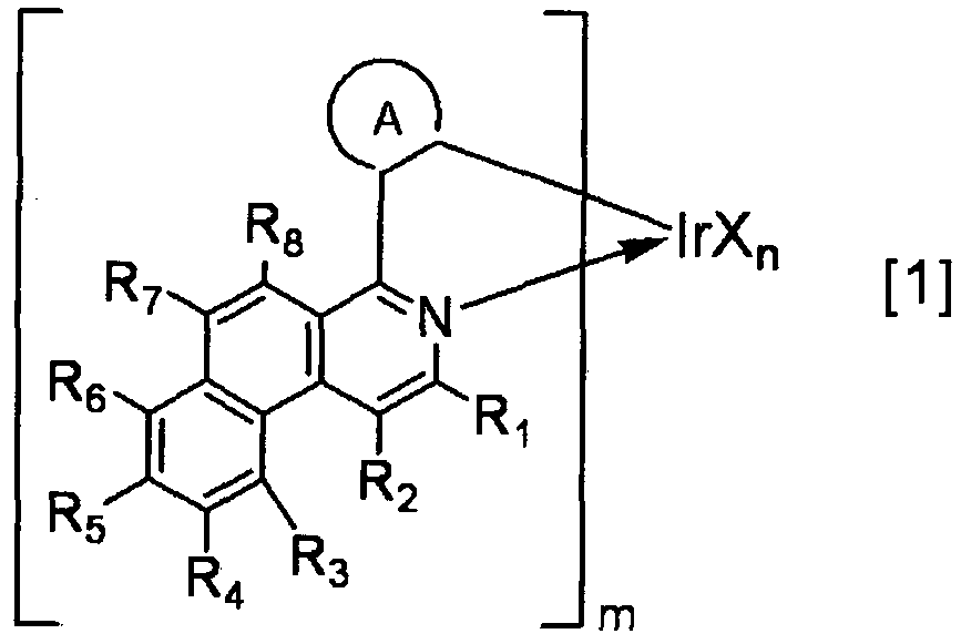
Ar-(Ar2)p-(Ar3)q-Ar, [5]
[0044] It is to be noted that in the present invention, an
iridium complex represented by the following general formula [6] may be incorporated instead of the iridium complex represented by the general formula [1] into the organic compound layer, and a hydrocarbon compound represented by the following general formula [10] may be incorporated instead of the hydrocarbon compound represented by the general formula [5] into the layer.
[0045]

Ar5- (Ar6) r~ (Ar7) S-Ar8 [10]
[0046] It is to be noted that details about the iridium
complex represented by each of the general formulae [1] and [6] and the hydrocarbon compound represented by each of the general formulae [5] and [10] are described later.
[0047] Hereinafter, the organic light-emitting device of the present invention is described with reference to the drawings .
[0048] FIGS. 1A to 1C are schematic sectional views
illustrating organic light-emitting devices according to exemplary embodiments of the present invention, FIG. 1A being a view illustrating a first embodiment, FIG. IB being a view illustrating a second embodiment, and FIG. 1C being a view illustrating a third embodiment. First, reference numerals in the figures are described. An organic light-emitting device is represented by reference numeral 1 (2, 3), a display apparatus is represented by reference numeral 4, a substrate is represented by reference numeral 10, a base material is represented by reference numeral 11, a TFT driving circuit is represented by reference numeral 12, a planarizing layer is represented by reference numeral 13, a pixel separation film is represented by reference numeral 14, an organic red-light-emitting device is
represented by reference numeral 20R, an organic green- light-emitting device is represented by reference numeral 20G, an organic blue-light-emitting device is represented by reference numeral 20B, an anode is represented by reference numeral 21, a reflecting electrode layer is represented by reference numeral 21a, a transparent electrode layer is represented by
reference numeral 21b, an emission layer is represented by reference numeral 22, a red-light-emitting layer is represented by reference numeral 22R, a green-light- emitting layer is represented by reference numeral 22G, a blue-light-emitting layer is represented by reference numeral 22B, an electron-injecting/transporting layer is represented by reference numeral 23, a cathode is represented by reference numeral 24, a hole- injecting/transporting layer is represented by
reference numeral 25, an electron/exciton-blocking layer is represented by reference numeral 26, an
encapsulating film is represented by reference numeral 30, an encapsulating glass 40 is represented by
reference numeral 40, and a circularly polarizing plate is represented by reference numeral 50.
[0049] In the organic light-emitting device 1 of FIG. 1A, the anode 21, the emission layer 22, the electron- in ecting/transporting layer 23, and the cathode 24 are provided in the stated order on the substrate 10. The organic light-emitting device 1 of FIG. 1A is useful when the emission layer 22 has all of hole-transporting performance, electron-transporting performance, and light-emitting performance. In addition, the organic light-emitting device 1 of FIG. 1A is also useful when a hole-transporting material, an electron-transporting material, and a light-emitting material are mixed in the emission layer 22.
[0050]The organic light-emitting device 2 of FIG. IB is
different from the organic light-emitting device 1 of
FIG. 1A in that the hole-injecting/transporting layer 25 is provided between the anode 21 and the emission . layer 22. In the organic light-emitting device 2 of FIG. IB, a layer having a carrier-transporting function and a layer having "a light-emitting function are separated from each other, and hence compounds having respective characteristics, i.e., hole-transporting property, electron-transporting property, and light- emitting property can be used in combination as
appropriate. Accordingly, the degree of freedom in material selection extremely increases and emission efficiency can be improved by effectively trapping each charge or exciton in the central emission layer 22.
[0051] The organic light-emitting device 3 of FIG. 1C is
different from the organic light-emitting device 2 of FIG. IB in that the electron/exciton-blocking layer 26 is provided between the emission layer 22 and the hole- injecting/transporting layer 25. The organic light- emitting device 3 of FIG. 1C is provided with the electron/exciton-blocking layer 26 and hence an
electron can be trapped in the emission layer 22.
Accordingly, as in FIG. IB, the emission efficiency can be improved.
[0052] It is to be noted that the organic light-emitting
devices illustrated in FIGS. 1A to 1C are only very basic device constructions and the present invention is not limited thereto. For example, the following various layer constructions can each be adopted: an insulating layer, an adhesion layer, or an interference layer is provided at an interface between an electrode and the organic compound layer, or the hole- transporting layer is constituted of two layers having different HOMO ' s or ionization potentials.
[0053] In addition to the constructions illustrated in FIGS.
1A to 1C, examples of the device construction of the organic light-emitting device include the following
constructions (1) to (5) . It is to be noted that in each of the device constructions, the organic compound layer necessarily includes an emission layer including a light-emitting material.
(1) (Substrate/) anode/emission layer/cathode
(2) (Substrate/) anode/hole-transporting layer/emission layer/electron-transporting layer/cathode
(3) (Substrate/) anode/hole-transporting layer/emission layer/electron-transporting layer/cathode (FIG. IB))
(4) (Substrate/) anode/hole-injecting layer/hole- transporting layer/emission layer/electron-transporting layer/cathode
(5) (Substrate/) anode/hole-transporting layer/emission layer/hole/exciton-blocking layer/electron-transporting layer/cathode
[0054] In the present invention, the aspect according to which light output from the emission layer is extracted
(device form) may be the so-called bottom emission system in which the light is extracted from an
electrode on a side closer to the substrate or may be the so-called top emission system in which the light is extracted from a side opposite to the substrate. In addition, a double-face extraction system (tandem system) in which the light is extracted from each of the side closer to the substrate and the side opposite to the substrate can be adopted.
[0055] In the organic light-emitting device of the present
invention, the iridium complex represented by the general formula [1] (or [6])· and the hydrocarbon compound represented by the general formula [5] (or
[10]) are preferably incorporated into the emission layer out of the organic compound layer. In this case, the emission layer includes at least the iridium complex represented by the general formula [1] (or [6]) and the hydrocarbon compound represented by the general formula [5] (or [10]). The applications of the
compounds to be incorporated into the emission layer in this case vary depending on their content
concentrations in the emission layer. Specifically, the compounds are classified into a main component and a sub-component depending on their content
concentrations in the emission layer.
[0056] he compound serving as the main component is a
compound having the largest weight ratio (content concentration) out of the group of compounds to be incorporated into the emission layer and is a compound also. called a host. In addition, the host is a
compound present as a matrix around the light-emitting material in the emission layer, and is a compound mainly responsible for the transport of a carrier to the light-emitting material and the donation of an excitation energy to. the light-emitting material.
[0057] In addition, the compound serving as the sub-component is a compound except the main component and can be called a guest (dopant) , a light emission assist material, or a charge-injecting material depending on a function of the compound. The guest as one kind of sub-component is a compound (light-emitting material) responsible for main light emission in the emission layer. The light emission assist material as one kind of sub-component is a compound that assists the light emission of the guest and is a compound having a smaller weight ratio (content concentration) in the emission layer than that of the host. The light emission assist material is also called a second host by virtue of its function.
[0058] The concentration of the guest with respect to the host is preferably 0.1 wt% or more and 20 wt% or less, more preferably 1 wt% or more and 15 wt% or less with reference to the total amount of the constituent materials for the emission layer.
[0059] (2) Iridium complex
Next, the iridium complex as one constituent material for the organic light-emitting device of the present invention is described. The iridium complex as one constituent material for the organic light-emitting device of the present invention is a compound
represented by the following general formula [1] or the following general formula [6] .
[0060]

[0061] It is to be noted that the basic skeleton of the
iridium complex represented by the general formula [6] is the same as that of the iridium complex represented by the general formula [1] . In addition, the
substituents represented in the general formula [6], i.e., R31 to R38 correspond to Ri to R8 in the general formula [1] , respectively. Further, k and 1 in the general formula [6] correspond to m and n in the general formula [1] , respectively. Hereinafter, the iridium complex represented by the general formula [1] is mainly described.
[0062] In the formula [1], Ri to R8 each represent a hydrogen atom, a halogen atom, an alkyl group, an alkoxy group, a trifluoromethyl group, a cyano group, a substituted or unsubstituted aromatic hydrocarbon group, or a substituted or unsubstituted heteroaromatic group.
[ 0063 ] Specific examples of the halogen atom represented by any one of Ri to Rs include fluorine, chlorine, bromine, and iodine atoms.
[0064] he alkyl group represented by any one of Ri to R8 is
preferably an alkyl group having 1 or more and 6 or less carbon atoms.. Specific examples of the alkyl group having 1 or more and 6 or less carbon atoms include a methyl group, an ethyl group, an n-propyl group, an i-propyl group, an n-butyl group, an i-butyl group, a sec-butyl group, a tert-butyl group, an n- pentyl group, an i-pentyl group, a tert-pentyl group, a neopentyl group, an n-hexyl group, and a cyclohexyl group. It is to be noted that part or all of hydrogen atoms in the alkyl group may be substituted with a fluorine atom as in a trifluoromethyl group or the like. Of those alkyl groups, a methyl group or a tert-butyl group is particularly preferred.
[0065] Specific examples of the alkoxy group represented by
any one of Ri to ί½ include, but, of course, not limited to, a methoxy group, an ethoxy group, an i-propoxy group, an n-butoxy group, and a tert-butoxy group. Of those alkoxy groups, a methoxy group or an ethoxy group is preferred.
[0066] Specific examples of the aromatic hydrocarbon group
represented by any one of Ri to Rs include, but, of course, not limited to, a phenyl group, a naphthyl group, a phenanthryl group, an anthryl group, a
fluorenyl group, a biphenylenyl group, an
acenaphthylenyl group, a chrysenyl group, a pyrenyl group, a triphenylenyl group, a picenyl group, a
fluoranthenyl group, a perylenyl group, a naphthacenyl group, a biphenyl group, and a terphenyl group. Of those aromatic hydrocarbon groups, a phenyl group, a naphthyl group, a fluorenyl group, or a biphenyl group is preferred, and a phenyl group is more preferred.
[ 0067 ] Specific examples of the heteroaromatic group
represented by any one of Ri to R8 include, but, of course, not limited to, a thienyl group, a pyrrolyl group, a pyrazinyl group, a pyridyl group, an indolyl group, a quinolyl group, an isoquinolyl group, a
naphthyridinyl group, an acridinyl group, a phenanthrolinyl group, a carbazolyl group, a
benzo [a] carbazolyl group, a benzo [b] carbazolyl group, a benzo [c] carbazolyl group, a phenazinyl group, a
phenoxazinyl group, a phenothiazinyl group, a
benzothiophenyl group, a dibenzothiophenyl group, a benzofuranyl group, a dibenzofuranyl group, an oxazolyl group, and an oxadiazolyl group.
he aromatic hydrocarbon group and heteroaromatic group represented by Ri to R8 may each further have a
substituent. Specific examples thereof include: alkyl groups such as a methyl group, an ethyl group, an n- propyl group, an i-propyl group, an n-butyl group, an i-butyl group, a sec-butyl group, a tert-butyl group, an n-pentyl group, an i-pentyl group, a tert-pentyl group, a neopentyl group, an n-hexyl group, and a cyclohexyl group; a halogen atom selected from fluorine, chlorine, bromine, and iodine atoms; alkoxy groups such as a methoxy group, an ethoxy group, an i-propoxy group, an n-butoxy group, and a tert-butoxy group; substituted amino groups such as an N-methylamino group, an N- ethylamino group, an N, N-dimethylamino group, an N,N- diethylamino group, an N-methyl-N-ethylamino group, an N-benzylamino group, an N-methyl-N-benzylamino group, an N, -dibenzylamino group, an anilino group, an N,N- diphenylamino group, an N, N-dinaphtylamino group, an N, N-difluorenylamino group, an N-phenyl-N-tolylamino group, an N, N-ditolylamino group, an N-methyl-N- phenylamino group, an N, N-dianisoylamino group, an N- mesityl-N-phenylamino group, an N, N-dimesitylamino group, an N-phenyl-N- ( 4-tert-butylphenyl ) amino group, and an N-phenyl-N- ( 4-trifluoromethylphenyl ) amino group; aromatic hydrocarbon groups such as a phenyl group, a naphthyl group, a phenanthryl group, an anthryl group, a fluorenyl group, a biphenylenyl group, an
acenaphthylenyl group, a chrysenyl group, a pyrenyl
group, a triphenylenyl group, a picenyl group, a fluoranthenyl group, a perylenyl group, a naphthacenyl group, a biphenyl group, and a terphenyl group;
heteroaromatic groups such as a thienyl group, a
pyrrolyl group, a pyrazinyl group, a pyridyl group, an indolyl group, a quinolyl group, an isoquinolyl group, a naphthyridinyl group, an acridinyl group, a
phenanthrolinyl group, a carbazolyl group, a
benzo [a] carbazolyl group, a benzo [b] carbazolyl group, a benzo [c] carbazolyl group, a phenazinyl group, a
phenoxazinyl group, a phenothiazinyl group, a
benzothiophenyl group, a dibenzothiophenyl group, a benzofuranyl group, a dibenzofuranyl group, an oxazolyl group, and an oxadiazolyl group; a cyano group; and a trifluoromethyl group. Of those substituents , a methyl group, a tert-butyl group, a phenyl group, a naphthyl group, a fluorenyl group, or a biphenyl group is
preferred, and a phenyl group is more preferred.
[0069] In the formula [1], m represents an integer of 1 to 3 and n represents an integer of 0 to 2, provided that m+n equals 3.
[0070] In the formula [1], the ring A represents a cyclic
structure selected from a benzene ring, a naphthalene ring, a fluorene ring, a phenanthrene ring, a 9,9- spirobifluorene ring, and a chrysene ring. The ring A is bonded to a benzo [ f] isoquinoline skeleton and . an Ir metal with respective covalent bonds.
[0071] It is to be noted that the ring A may further have a
substituent. Specific examples thereof include: alkyl groups such as a methyl group, an ethyl group, an n- propyl group, an i-propyl group, an n-butyl group, an i-butyl group, a sec-butyl group, a tert-butyl group, an n-pentyl group, an i-pentyl group, a tert-pentyl group, a neopentyl group, an n-hexyl group, and a cyclohexyl group; a halogen atom selected from fluorine, chlorine, bromine, and iodine atoms; alkoxy groups such
as a methoxy group, an ethoxy group, an i-propoxy group an n-butoxy group, and a tert-butoxy group; substituted amino groups such as an N-methylamino group, an N- ethylamino group, an N, N-dimethylamino group, an N,N- diethylamino group, an N-methyl-N-ethylamino group, an N-benzylamino group, an N-methyl-N-benzylamino group, an N, N-dibenzylamino group, an anilino group, an N,N- diphenylamino group, an N, N-dinaphtylamino group, an N, N-difluorenylamino group, an N-phenyl-N-tolylamino group, an N, N-ditolylamino group, an N-methyl-N- phenylamino group, an N, N-dianisoylamino group, an N- mesityl-N-phenylamino group, an N, N-dimesitylamino group, an N-phenyl-N- (4-tert-butylphenyl) amino group, and an N-phenyl-N- ( 4-trifluoromethylphenyl ) amino group; aromatic hydrocarbon groups such as a phenyl group, a naphthyl group, a phenanthryl group, an anthryl group, a fluorenyl group, a biphenylenyl group, an
acenaphthylenyl group, a chrysenyl group, a pyrenyl group, a triphenylenyl group, a picenyl group, a fluoranthenyl group, a perylenyl group, a naphthacenyl group, a biphenyl group, a terphenyl group, a
dimethylphenyl group, a tert-butylphenyl group, a cyanophenyl group, a trifluoromethylphenyl group, and a methoxyphenyl group; heteroaromatic groups such as a thienyl group, a pyrrolyl group, a pyrazinyl group, a pyridyl group, an indolyl group, a quinolyl group, an isoquinolyl group, a naphthyridinyl group, an acridinyl group, a phenanthrolinyl group, a carbazolyl group, a benzo [a] carbazolyl group, a benzo fb] carbazolyl group, a benzo [c] carbazolyl group, a phenazinyl group, a
phenoxazinyl group, a phenothiazinyl group, a
benzothiophenyl group, a dibenzothiophenyl group, a benzofuranyl group, a dibenzofuranyl group, an oxazolyl group, an oxadiazolyl group, and a dimethylpyridyl group; a cyano group; and a trifluoromethyl group.
] In the formula [1], X represents a bidentate ligand.
In the formula [1], a partial structure IrXn of the complex including X is specifically any one of the structures represented by the following general
formulae [2] to [4] .
[0073]

[0074] It is to be noted that, in the formula [6], a partial structure IrXi of the complex including X is
specifically any one of the structures represented by the following general formulae [7] to [9].
[0075]

[0076]Here, the basic skeletons of the structures represented by the general formulae [7] to [9] are the same as those of the general formulae [2] to [4], respectively. In addition, the substituents represented in the general formulae [7] to [9], i.e., R39 to R53 correspond to Rio to R24 in the general formulae [2] to [4], respectively. Hereinafter, the structures represented by the general formulae [ 2 } to [4] are mainly described
[0077] In the formulae [2] to [4], Rio to R24 each represent a hydrogen atom, a halogen atom, an alkyl group, an alkoxy group, a trifluoromethyl group, a cyano group, a substituted or unsubstituted aromatic hydrocarbon group
or a substituted or unsubstituted heteroaromatic group.
[0078] Specific examples of the halogen atom, alkyl group,
alkoxy group, trifluoromethyl group, cyano group, aromatic hydrocarbon group, and heteroaromatic group represented by Rio to R24 are the same as the specific examples in Ri to R8 in the general formula [1] . In addition, when the substituent represented by any one of Rio to R24 is an aromatic hydrocarbon group or a heteroaromatic group, specific examples of the
substituent that the substituent may further have are the same as the specific examples in Ri to Rs in the general formula [1].
[0079] In the iridium complex represented by the general
formula [1] , m preferably represents 2 and n preferably represents 1.
[0080] n addition, the iridium complex represented by the
general formula [1] (general formula [6]) is preferably an iridium complex represented by the following general formula [ 11] .
[0081]

[0082] In the formula [11], R6i to R71 each represent a
hydrogen atom, a halogen atom, an alkyl group, an alkoxy group, a trifluoromethyl group, a cyano group, a substituted or unsubstituted aromatic hydrocarbon group, or a substituted or unsubstituted heteroaromatic group.
[ 0083 ] Specific examples of the halogen atom, alkyl group,
alkoxy group, trifluoromethyl group, cyano group, aromatic hydrocarbon group, and heteroaromatic group
represented by R6i to R71 are the same as the specific examples of Rj. to R8 in the general formula [1] . .In addition, when the substituent represented by any one of R6i to R7 i is an aromatic hydrocarbon group or a heteroaromatic group, specific examples of the
substituent that the aromatic hydrocarbon group and the heteroaromatic group may each further have are the same as the specific examples of Ri to R8 in the general formula [1] .
[0084] In the formula [11], m represents an integer of 1 to 3 and n represents an integer of 0 to 2, provided that m+n equals 3.
[0085] In the formula [11], *1 represents a bond between the ring A and the Ir metal and *2 represents a bond between the ring A and a carbon atom at the 1-position of the benzo [ f] isoquinoline skeleton.
[0086] In the formula [11], the ring A is a substituted or unsubstituted aromatic ring, is specifically a partial structure represented by any one of the following general formulae [12] to [16], and is preferably a structure represented by the general formula [12].
[0087]

[0089] Specific examples of the halogen atom, alkyl group,
alkoxy group, trifluoromethyl group, cyano group, aromatic hydrocarbon group, and heteroaromatic group represented by R72 to R93 are the same as the specific examples of Ri to Rs in the general formula [1] . In addition, when the substituent represented by any one of R72 to R93 is an aromatic hydrocarbon group or a heteroaromatic group, specific examples of the
substituent that the substituent may further have are the same as the specific examples of Rx to R8 in the general formula [1] .
[0090] In the formulae [12] to [16], *1 represents a bonding position with the Ir metal and *2 represents a bonding position with the carbon atom at the 1-position in the benzo [f ] isoquinoline skeleton.
[0091] In addition, the iridium complex represented by the
general formula [1] is particularly preferably an iridium complex represented by the following general formula [17] .
[0092]

specific examples in Ri to Rs in the general formula [1].
[0094] In the formula [17], G represents a hydrogen atom, a
halogen atom, an alkyl group, an alkoxy group, a
trifluoromethyl group, a cyano group, or a substituted or unsubstituted phenyl group. Specific examples of the halogen atom, alkyl group, and alkoxy group
represented by G, and the substituent that the phenyl group represented by G may further have are the same as the specific examples in Ri to R8 in the general formula - [1].
[0095] (3) Hydrocarbon compound serving as host
Next, the hydrocarbon compound to be used as the host is described. The hydrocarbon compound to be used as the host is any one of the hydrocarbon compounds
represented by the following general formula [5] or the following general formula [10].
[0096]
Ar5-(Ar6)r-(Ar7)s-Ar8 [10]
[0097] In the formula [5], p and q each represent 0 or 1. In addition, in the formula [5] , p+q is equal to or more than 1.
[0098]Ari represents any one of the substituents represented in the following substituent group a.
[0099]Ar2 and Ar3 each represent any one of the substituents represented in the following substituent group β. Ar2 and Ar3 may be identical to or different from each other .
[0100]
[Substituent group a]

[Substituent group β]

[0101] In the formula [10], r and s each represent 0 or 1. In addition, in the formula [10], r+s is egual to or more than 1.
[0102]Ar5 represents any one of the substituents represented in the following substituent group a' .
[0103]Ar6 and Ar7 each represent any one of the substituents . represented in the following substituent group β' . Ar6 and Ar7 may be identical to or different from each other .
[0104 ]Ar8 represents any one of the substituents represented in the following substituent group γ' .
Substituent group

[Substituent group γ' ]
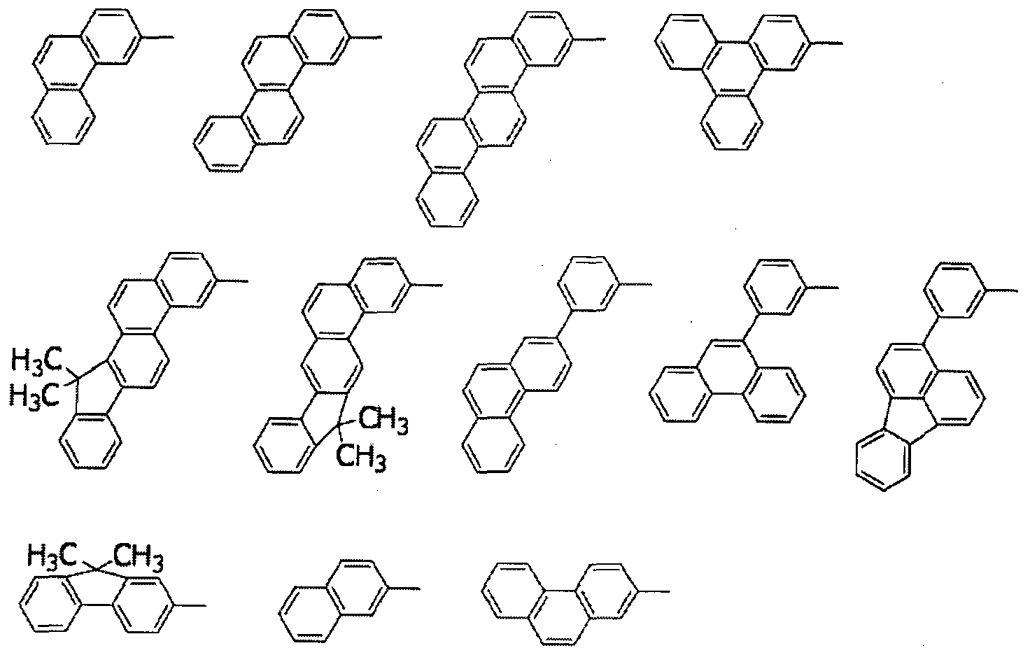 [0106] (4) Third component
In the present invention, the organic compound layer (preferably the emission layer) contains the iridium complex represented by the general formula [1] and the hydrocarbon compound represented by the general formula [5], or the iridium complex represented by the general formula [6] and the hydrocarbon compound represented by the general formula [10], provided that in addition to the iridium complex and the hydrocarbon compound, a material serving as a third component may be
incorporated into the organic compound layer together with the complex and the compound.
[0107] In the present invention, a compound serving as the
third component is a material having the following feature (4-1), (4-2), or (4-3):
(4-1) a material having a larger (shallower) HOMO level than the HOMO level of the host;
(4-2) a material having an LUMO level smaller in energy (deeper) than the LUMO level of the host; or
(4-3) a material having an HOMO level larger in energy than the HOMO level of the host and having an LUMO level smaller in energy than the LUMO level of the host.
[0108] The material having the feature (4-1) facilitates the injection and transport of a hole into the emission layer by virtue of its shallow HOMO level. As a result, a reduction in drive voltage of the device is achieved and the light-emitting material can be suppressed from being excessively brought into an anion state, and hence the lifetime of the device is lengthened.
[0109] The material having the feature (4-2) lengthens the
lifetime of the device by the following reason. That is, the LUMO level of the host is shallower (larger in energy) than that of the light-emitting material, and hence the addition of the third component having a deeper LUMO level than the LUMO level of the host can suppress the light-emitting material from being
excessively brought into an anion state. Therefore, the lifetime is lengthened.
[0110] he material having the feature (4-3) can improve the hole-injecting property and alleviate electron trapping by the light-emitting material. As a result, the lifetime is lengthened.
[0111] It is to be noted that specific examples of the third component are described later.
[0112] (5) Operations and effects exhibited by host and guest The iridium complexes represented by the general formulae [1] and [6] each of which is to be used as a constituent material for the organic light-emitting device in the present invention each have a
phenylbenzo [ f ] isoquinoline ligand as a main ligand. Here, the basic skeleton of phenylbenzo [f] isoquinoline has the following feature: the conjugate surface of a n orbital is extended as compared with a phenylquinoline ligand or phenylisoquinoline ligand as a ligand of a conventional and typical red-light-emitting material by the condensation of a benzene ring with quinoline.
However, the structural feature leads to a reduction in emission efficiency or durability because of the following reason: an interaction with a material
(especially the host) near the light-emitting material is liable to occur, and the charge of the host is trapped to cause the transition of the light-emitting material to a radical state or the formation of an exciplex by the light-emitting material and the host.
[0113] In view of the foregoing, the inventors of the present invention have selected a compound having a unit that forms a band gap and a unit that reduces an
intermolecular interaction as a compound to be used as the host for avoiding the formation of an exciplex and the transition to a radical state.
[0114] The inventors have found that the design of the
compound which has those two units and the entire
molecule of which is chemically stable can improve the efficiency and drive durability of the organic light- emitting device.
[0115] FIG. 2 is a schematic view illustrating the model of a hydrocarbon compound to be used as the host. The molecular model illustrated in FIG. 2 has a unit Ul that forms a band gap and a unit U2 that reduces an intermolecular interaction. Here, the unit Ul is more specifically a partial structure having the following feature (5-1) . In addition, the unit U2 is more
specifically a partial structure having the following feature (5-2) or the following features (5-2) and (5-3). (5-1) A partial structure that forms a linear structure (5-2) A partial structure having a long axis in a direction different from the long axis direction of the unit Ul
(5-3) Parts at terminals are different from each other.
[0116] Further , it is because the hydrocarbon compound serving as the host in the present invention has the following feature (5-4) or the following features (5-4) and (5-5) that the compound is chemically stable:
(5-4) the compound is a molecule formed only of a hydrocarbon; and
(5-5) the compound is a molecule formed only of an sp2 carbon atom and a hydrogen atom.
[0117] Hereinafter, the. features (5-1) to (5-5) are described.
[0118] (5-1) Partial structure that forms linear structure
The band gap of the host needs to be properly designed in order that excessive transition of the light- emitting material to a radical state may be avoided.
In the present invention, red light as light to be output by the organic light-emitting device is light whose emission peak wavelength falls within the range of 580 nm to 650 nm (1.9 eV to 2.1 eV in terms of the lowest triplet excited level (Ti) ) . Although it is essential for the i of the host to be higher than that
of the light-emitting material, the lowest singlet excited level (Si) and the band gap necessarily
increase when the ΊΊ is excessively high. Accordingly, charge accumulation occurs at an interface between the host and a peripheral material, or differences in highest occupied molecular orbital (HOMO) and lowest unoccupied molecular orbital (LUMO) levels between the host and the light-emitting material enlarge. As a result, the light-emitting material may serve as a charge trap to promote the deterioration of the light- emitting material. Further, the light-emitting
material having a phenylbenzoisoquinoline skeleton (iridium complex) to be used in the present invention easily traps charge probably because its LUMO orbital is extended as described above. Therefore, a host having a narrow band gap is preferably selected so that the injection and transport of charge may be smoothly performed. Table 1 below is a table showing the Τχ energies and AS-T values of main aromatic rings when used alone.
able 1
Ti AS-T
Structural formula
[eV] [eV]
Benzene 3.7 1.1
Naphthalene 2.6 1.4.
Phenanthrene 2.7 0.90
2.9 1.2
Fluorene
Triphenylene 2.9 0.72
Chrysene 2.5 0.95
Picene 2.5 0.81
1.8 1.5
Anthracene
Pyrene 2.1 1.2
[0120] Of the aromatic rings listed above, benzene,
naphthalene, phenanthrene, fluorene, triphenylene, chrysene, and picene are preferred.
[0121] In addition, in consideration of a requirement for the Ti of the host and the AS-T value (energy difference between the Si and the Ti) of the hydrocarbon compound, the band gap of the host is preferably 2.7 eV to 3.6 eV, more preferably 2.7 eV to 3.4 eV.
[0122] It is understood from the foregoing that the following features (5-la) and (5-lb) are important for achieving the suitable range of the band gap in the host:
(5-la) conjugation is extended; and
(5-lb) a hydrogen atom bonded to the peri-position is absent .
[0123] herefore, the host preferably has a structure
represented by the general formula [5] (or the general formula [10]). In addition, Ar2 and Ar3 in the general formula [5] each preferably represent any one member selected from the following partial structure group.
[0124]

In addition, Ar5 and Ar6 in the general formula [10] each preferably represent any one member selected from the following partial structure group..

[0125]As represented in the general formula [5] (or the
general formula [10]), Ar2 and Ar3 in the general
formula [5] (or Ar6, Ar7 in the general formula [10] ) each represent an arylene group having a bonding hand at such a site that conjugation is extended (the band gap reduces) with respect to Ari as a terminal aryl group.
[0126] In addition, in a bond with each of Ari(or Ar5) bonded to Ar2 (or Are) and i (or Ar8) bonded to Ar3(or Ar7) , a hydrogen atom bonded to the peri-position is preferably absent. This is because of the following reason: when the hydrogen atom bonded to the peri-position is absent, the dihedral angle of the bond between the respective units reduces and the p orbitals of the respective carbon atoms are in parallel contact with each other, and hence the conjugation length of the entire molecule extends. For example, when naphthalene having bonding hands at its 2-position and 6-position represented above, and naphthalene having bonding hands at its 1- position and 4-position are compared, the relative directions of the two bonding hands of each naphthalene are the same. However, in naphthalene having bonding hands at its 1-position and 4-position, repulsion between substituents enlarge owing to hydrogen atoms bonded to carbon atoms at the 5-position and 8-position in its skeleton, and hence the dihedral angle enlarges. As a result, the extent to which the p orbitals overlap
each other reduces and the conjugation no longer extends, and hence the band gap increases.
[0127] In addition, the number (p or r) of Ar2 ' s or Ar6's and the number (q or s) of Ar3 ' s or Ar7 ' s desirably have a relationship of l≤p+q≤2 (l≤r+s≤2) . When p+q (r+s) exceeds 2, the molecular weight of the host increases and its sublimability reduces, with the result that the reduction of its purity may occur.
[0128] In consideration of the conditions, a compound to be obtained is a material having a band gap suitable for a red color, charge-injecting property improves, and the charge accumulation can be avoided.
[0129] (5-2) Partial structure having long axis in direction different from long axis direction of unit Ul
The feature (5-2) is description concerning the partial structures Ari (or Ars, A e) · Here, in the case where the substituents represented by Ari (or Ar5, Ar8) in the general formula [5] (or the general formula [10]) are selected from the same group as that of Ar2 and Ar3(or Ar6, Ar7 in the general formula [10]), the structure of the entire molecule of the designed compound becomes linear. In this case, turning the designed compound into a film shape causes the materials to closely adhere to each other. In particular, the iridium complex (light-emitting material) represented by the general formula [1] to be used in the present invention receives an electron from the host to which the complex closely adheres, and is easily brought into a radical state probably because its LUMO orbital is extended.
[0130] In view of the foregoing, it has been found that the following is optimum in the present invention: aryl groups are bonded to each other so that the long axis directions of Ari (or Ar5, Ar9) may be different from the long axis directions of Ar2(or Ar6) and Ar3(or Ar7) . Specifically, the substituents represented by Ari are selected from aryl groups represented in the following
substituent group.
[0131]

In addition, the substituents represented by Ar5 are selected from aryl groups represented in the following substituent group.
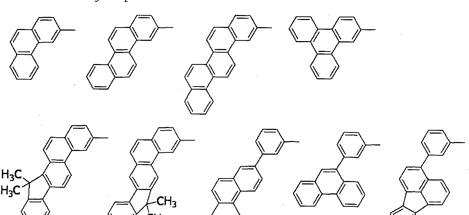
[0132] It is to be noted that Ar8 is selected from aryl groups represented in the substituent group and the following substituent group.
[0133]
 [0134] In that case, the conjugation length of the entire molecule of the hydrocarbon compound serving as the host is extended by Ar2 (or Ar6) and Ar3 (or Ar7) , and hence the compound forms a band gap suitable for a red color. In addition, the long axis direction of Ari (or Ar5, Ar8) at each terminal is different from the long axis directions of Ar2(or Ar6) and Ar3 (or Ar7) . As a result, the structure of the entire molecule becomes a twisted structure as illustrated in FIG. 2. Therefore, the close adhesion between the materials is suppressed and hence the light-emitting material can be prevented from being brought into a radical state.
[0135] (5-3) Parts at terminals are different from each other In the present invention, the aryl groups (Ar5) at the terminals of the host are more preferably different from each other as represented by the general formula [10] . Its symmetry is lower than that of the
hydrocarbon compound represented by the general formula [5] in which the aryl groups (Ar5) at the terminals are identical. Accordingly, the stacking of its molecules is avoided and hence the light-emitting material can be additionally prevented from being excessively brought into a radical state.
[0136] (5-4) Compound is molecule formed only of hydrocarbon
In general, the light-emitting material whose conjugate surface has been extended easily overlaps the host and hence their intermolecular interaction enlarges. As a result, an exciplex is formed, which may be responsible for the deterioration of the emission efficiency and durable characteristic. In addition, a carbon-carbon bond of the compound serving as the host has a stronger bonding strength than that of a carbon-nitrogen bond. For example, the energy of a bond between carbon and nitrogen calculated for 4 , 4 ' -di ( 9H-carbazol-9-yl) -1, 1 ' - biphenyl (CBP) by means of b3-lyp/def2-SV ( P) is 3.86 eV (calculated value) as represented below.
[0137]

[0138] In contrast, the energy of a bond between carbon and carbon is 5.04 eV (calculated value). Therefore, the host is preferably formed only of a hydrocarbon considered to be strong in emission efficiency and durable characteristic.
[0139] (5-5) Compound is molecule formed only of sp2 carbon atom and hydrogen atom
The compound to be used as the host in the present invention is preferably a compound formed only of an sp2 carbon atom and a hydrogen atom. When all carbon atoms forming its basic skeleton are constituted of SP carbon atoms, structural changes from the ground state to the state of accumulation of charge and an excited state may be small. Accordingly, the polycyclic aromatic hydrocarbon compound may tend to be strong against deterioration even when brought into an unstable cation state by charge injected from an electrode. In addition, according to Bond et al. (see NPL 1), a carbon-carbon single bond has an energy of 3.9 eV and a carbon-carbon double bond has an energy o 7.5 eV, i.e., the bonding energy of the double bond is larger. It is assumed from the foregoing that the ■ compound formed only of an SP2 carbon atom and a hydrogen atom is a stable compound from the viewpoint of a chemical bond.
[0140] (6) Specific examples of iridium complex
Specific structural formulae of the iridium complex to be incorporated into the organic light-emitting device of the present invention are exemplified below.
[0141] [Group 1 compound]

lr-122 142] [Group 2 compound]

p 3 compound]

[0144] [Group 4 compound]

lr-412 lr-413 lr-414 lr-415
43

[0146]
[Group 5a compound]

lr-506 lr-507 lr-508
[Grou 5b compound]

[0147] Of the exemplified compounds, the iridium complexes represented by Ir-101 to Ir-123 are each an iridium complex in which all ligands are each a ligand including a benzo [ f] isoquinoline skeleton out of the iridium complexes each represented by the general formula [1] . The stability of each of those iridium
complexes in the group 1 itself is extremely high by virtue of the structure of the ligand
(arylbenzo [ f ] isoquinoline ligand) of the complex.
Therefore, the incorporation of any such complex as a guest into the emission layer provides a long-lifetime organic light-emitting device because the incorporation improves its drive durability.
[0148] Of the exemplified compounds, the iridium complexes represented by Ir-201 to Ir-226 are each an iridium complex in which G does not represent a substituted or unsubstituted phenyl group out of the iridium complexes each represented by the general formula [17]. Those iridium complexes in the group 2 are each a complex having an extremely high emission quantum yield and hence the incorporation of any such complex as a guest into the emission layer provides an organic light- emitting device having high emission efficiency.
Further, three ligands of each iridium complex in the group 2 include one acac-based ligand (diketone-based bidentate ligand) having a small molecular weight.
Accordingly, the complex has the following advantage: the complex can be easily subjected to sublimation purification because the molecular weight of the complex itself is relatively small.
[0149] Of the exemplified compounds, the iridium complexes represented by Ir-301 to Ir-322 are each an iridium complex in which G represents a substituted or
unsubstituted phenyl group out of the iridium complexes each represented by the general formula [17]. Those iridium complexes in the group 3 are each a complex having an extremely high emission quantum yield as in the iridium complexes in the group 2. Accordingly, the incorporation of any such complex as a guest into the emission layer improves the emission efficiency of the organic light-emitting device.
[0150] Of the exemplified compounds, the iridium complexes
represented by Ir-401 to Ir-429 are each an iridium complex represented by the general formula [1] in which m represents 2 and n represents 1, but the iridium complex does not correspond to any iridium complex represented by the general formula [17]. Those iridium complexes in the group 4 are each also a complex having an extremely high emission quantum yield as in the iridium complexes in the groups 2 and 3. Accordingly, the incorporation of any such complex as a guest into the emission layer improves the emission efficiency of the organic light-emitting device.
[0151] Of the exemplified compounds, the iridium complexes
represented by Ir-501 to Ir-508 are each an iridium complex represented by the general formula [1] in which the partial structure IrXn is represented by the
formula [3] . Those iridium complexes in the group 5a each contain, in a molecule thereof, one picolinic acid derivative as a ligand. Here, the introduction of the picolinic acid derivative as a ligand shifts the
emission peak wavelength of the complex itself to shorter wavelengths as compared with that in the case where the acac-based ligand is introduced.
[0152] Of the exemplified compounds, the iridium complexes
represented by Ir-509 to Ir-516 are each an iridium complex represented by the general formula [1] in which the partial structure IrXn is represented by the
formula [2] . Those iridium complexes in the group 5b each contain, in a molecule thereof, one or two
phenylpyridine (ppy) derivatives. Here, each iridium complex in the group 5b provides red light emission derived from the arylbenzo [f] isoquinoline ligand
because the ligand ppy is a non-light-emitting ligand. In addition, the ligand ppy has a smaller molecular weight than that of the arylbenzo [f] isoquinoline ligand. Accordingly, the complex has a smaller molecular weight than that of any iridium complex in the group 1 and
hence can be easily subjected to sublimation
purification. Therefore, the incorporation of any iridium complex in the group 5b as a guest into the emission layer as in any iridium complex in the group 1 can provide a long-lifetime organic light-emitting device.
[0153] By the way, the following structural isomers sterically exist for the iridium complex represented by the
general formula [1]: an fac form and an mer form.
Although the steric structure of the iridium complex represented by the general formula [1] is not
particularly limited in the present invention, the fac form generally credited with having a high quantum yield is preferred. However, in the case of an iridium complex in which two kinds of ligands having, different structures coordinate to an iridium atom, the mer form such as Ir(ppy)2acac may also have a high quantum yield. Accordingly, the fac form is not necessarily preferred. In addition, it is difficult to synthesize one of the structural isomers selectively at the time of the synthesis of the complex, and both isomers may be used as a mixture in terms of a cost.
[0154] (7) Specific examples of hydrocarbon compound (host)
Specific structural formulae of the hydrocarbon
compound to be incorporated as the host into the
organic light-emitting device of the present invention are exemplified below.


A- 105

B-105 Eh 106
[0157] [Grou C]

C-105
[0158] [Group D]

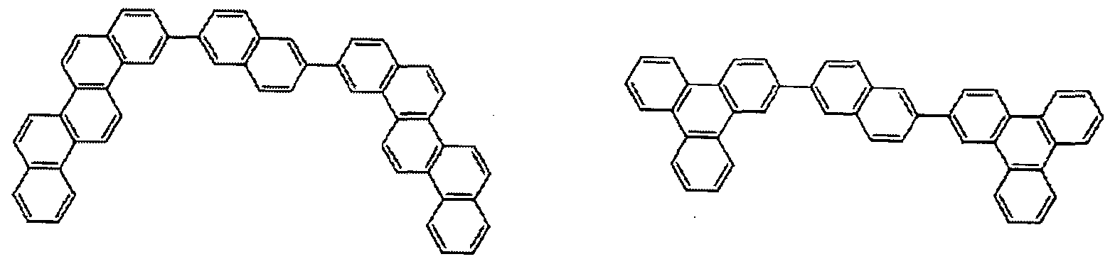

D 105
[0159] [Group E]

[0160] [Group F]

F -101 F 102


[0162] [Group H]
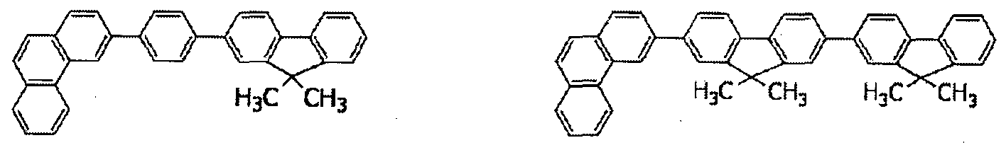
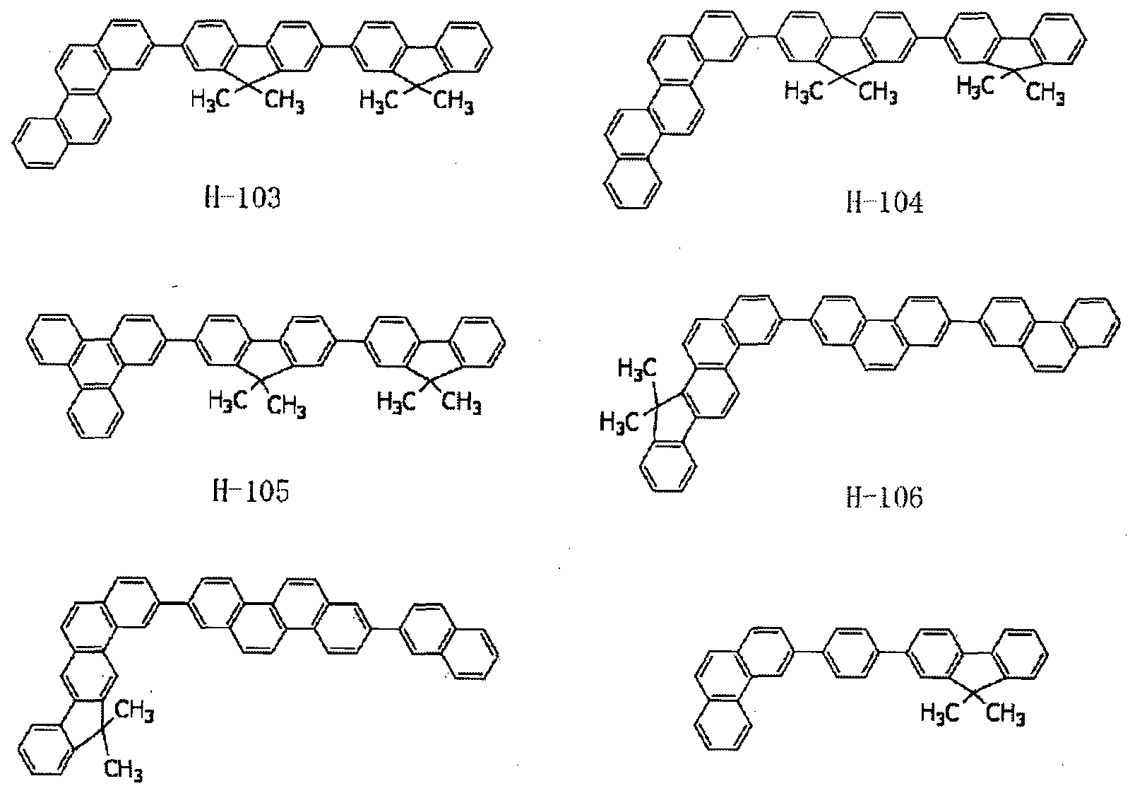
H 107
[0163] [Group I]
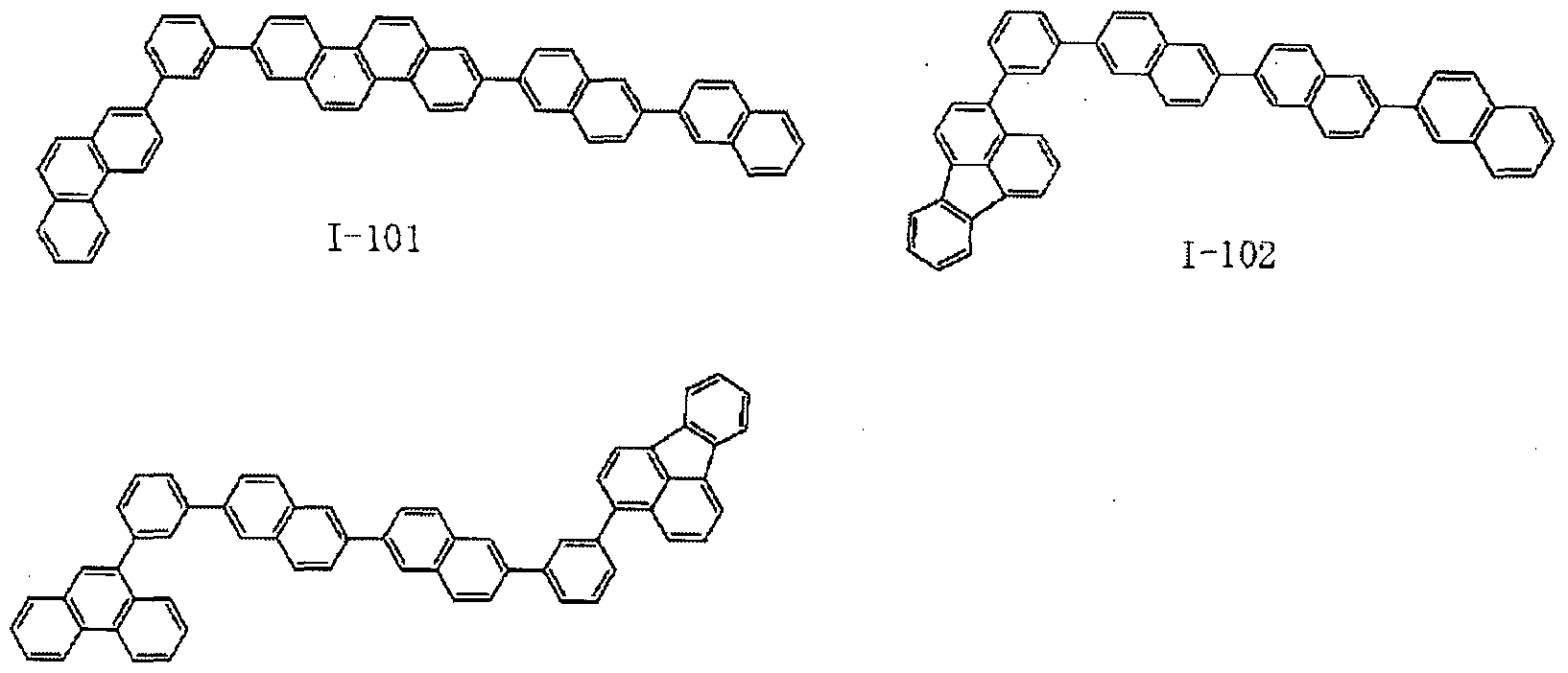
1-103
[0164] [Group J]


J-105
[0165] [Group K]

K 10:5 K 104
[0166] [Group L]


[0167]Each compound in the group A is a compound which has the features (5-1), (5-2), (5-4), and (5-5), in which p (or r) and q (or s) each represent 1, and which
contains a metaphenylene group. Each compound
belonging to the group A is a compound formed only of a hydrocarbon and all carbon atoms constituting its atoms are only SP2 carbons. Accordingly, the compound has the following feature: the compound is chemically stable and shows a small structural change, and is hence strong against deterioration. In addition, each compound belonging to the group A contains a
metaphenylene group, and hence molecular orbitals are localized at Ar2 (or Ar6) and Ar3 (or Ar7) , and ri (or Ar5, Ar8) becomes an unoccupied orbital. Accordingly, the compound also has the following feature: the extent to which the molecular orbitals overlap each other is small .
[0168] Each compound in the group B is a compound which has the features (5-1), (5-2), (5-4), and (5-5), in which p
(or r) and q (or s) each represent 1, but which does not contain any metaphenylene group. Each compound belonging to the group B is a compound formed only of a hydrocarbon and all carbon atoms constituting its atoms are only SP2 carbons as in the compounds in the group A. Accordingly, the compound has the following feature:
the compound is chemically stable and shows a small structural change, and is hence strong against
deterioration. In addition, each compound belonging to the group B does not contain any metaphenylene group, and hence only the terminal of Ari (or Ar5, Ar8) becomes an unoccupied orbital. Accordingly, the compound also has the following feature: its charge conductivity improves .
[0169] Each compound in the group C is a compound which has
the features (5-1), (5-2), (5-4), and (5-5), in which p (or r) represents 1 and q (or s) represents 0, and which contains a metaphenylene group. Each compound belonging to the group C tends to have a smaller
molecular weight (be lighter) because the number of its arylene groups is smaller than that of a compound in which p (or r) and q (or s) each represent 1. In addition, the number of rotation sites of a molecule thereof reduces because the number of the arylene groups is small. Therefore, the compound has the following features: its sublimability improves and the stability of the molecule improves. In addition, each compound belonging to the group C contains a
metaphenylene group, and hence molecular orbitals are localized at Ar2 (or Ar6) and Ar3 (or Ar ) , and Ari (or Ars, Ars) becomes an unoccupied orbital. Accordingly, the compound also has the following feature: the extent to which the molecular orbitals overlap each other is small .
[0170] Each compound in the group D is a compound which has
the features (5-1), (5-2), (5-4), and (5-5), in which p
(or r) represents 1 and q (or s) represents 0, but which does not contain any metaphenylene group. Each compound belonging to the group D tends to have a smaller molecular weight (be lighter) because the number of its arylene groups is smaller than that of a compound in which p (or r) and q (or s) each represent 1. In addition, the number of rotation sites of a molecule thereof reduces because the number of the arylene groups is small. Therefore, the compound has the following features: its sublimability improves and the stability of the molecule improves. In addition, each compound belonging to the group D does not contain any metaphenylene group, and hence only the terminal of Ari (or Ar5, Ar8) (or Ar4) becomes an unoccupied orbital. Accordingly, the compound also has the following
feature: its charge conductivity improves.
[0171] Each compound in the group E is a compound which has
the features (5-1), (5-2), (5-3), and (5-4), in which p (or r) and q (or s) each represent 1, and which
contains a metaphenylene group. Each compound
belonging to the group E is a material in which aryl groups at left and right terminals are different from each other, and hence has the following feature: the extent to which the molecules of the material overlap each other reduces. In addition, each compound in the group E contains SP3 carbon in a molecule thereof in some cases, and in any such case, its HOMO may be raised and its hole-injecting property may improve. In addition, each compound in the group E contains a metaphenylene group, and hence molecular orbitals are localized at Ar2 (or Ar6) and Ar3 (or Ar7) , and Arx (or Ar5, Ar8) becomes an unoccupied orbital. Accordingly, the compound also has the following feature: the extent to which the molecular orbitals overlap each other is small.
[0172] Each compound belonging to the group F is a compound
which has the features (5-1), (5-2), (5-3), and (5-4), in which p (or r) and q (or s) each represent 1, but which does not contain any metaphenylene group. Each compound belonging to the group F is a material in which aryl groups at left and right terminals are different from each other, and hence has the following feature: the extent to which the molecules of the material overlap each other reduces. In addition, each compound in the group F contains SP3 carbon in a
molecule thereof in some cases, and in any such case, its HOMO may be raised and its hole-injecting property may improve. Further, each compound belonging to the group F does not contain any metaphenylene group, and hence only the terminal of Ari (or Ar5, Ar8) becomes an unoccupied orbital. Accordingly, the compound also has the following feature: its charge conductivity improves. ] Each compound in the group G is a compound which has
■ the features (5-1), (5-2), (5-3), and (5-4), in which p (or r) represents 1 and q (or s) represents 0, and which contains a metaphenylene group. Each compound belonging to the. group G tends to have a smaller
molecular weight (be lighter) because the number of its arylene groups is smaller than that of a compound in which p (or r) and q (or s) each represent 1.
Therefore, the compound has the following features: its sublimability improves and the stability of a molecule thereof improves. In addition, each compound belonging to the group G is a material in which aryl groups at left and right terminals are different from each other, and hence has the following feature: the extent to which the molecules of the material overlap each other reduces. In addition, each compound in the group G contains SP3 carbon in a molecule thereof in some cases, and in any such case, its HOMO may be raised and its hole-injecting property may improve. Further, each compound belonging to the group G contains a
metaphenylene group, and hence molecular orbitals are localized at Ar2 (or Ar6) and Ar3 (or Ar7) , and Ari (or Ar5, Ar8) becomes an unoccupied orbital. Accordingly, the compound also has the following feature: the extent to which the molecular orbitals overlap each other is small .
[0174] Each compound in the group H is a compound which has the features (5-1), (5-2), (5-3), and (5-4), in which p (or r) represents 1 and q (or s) represents 0, but which does not contain any metaphenylene group. Each compound belonging to the group H tends to have a smaller molecular weight (be lighter) because the number of its arylene groups is smaller than that of a compound in which p (or r) and q (or s) each represent 1. Therefore, the compound has the following features: its sublimability improves and the stability of a molecule thereof improves. In addition, each compound belonging to the group H is a material in which aryl groups at left and right terminals are different from each other, and hence has the following feature: the extent to which the molecules of the material overlap each other reduces. In addition, each compound in the group H contains SP3 carbon in a molecule thereof in some cases, and in any such case, its HOMO may be raised and its hole-injecting property may improve. Further, each compound belonging to the group H does not contain any metaphenylene group, and hence only the terminal of Ari (or Ars, Arg) becomes an unoccupied orbital. Accordingly, the compound also has the following feature: its charge conductivity improves.
[0175] Each compound in the group I is a compound which has the features (5-1), (5-2), (5-3), (5-4), and (5-5), in which p (or r) and q (or s) each represent 1, and which contains a metaphenylene group. Each compound
belonging to the group I has the following features: the compound shows small structural changes in a
radical state and an excited state, and is hence stable; and aryl groups at left and right terminals are different from each other, and hence the extent to which the molecules of the material overlap each other reduces. In addition, each compound belonging to the group I contains a metaphenylene group, and hence molecular orbitals are localized at Ar2 (or Are) and Ar3 (or Ar7) , and Ari (or Ar5, Ar8) becomes an unoccupied orbital. Accordingly, the compound also has the
following feature: the extent to which the molecular orbitals overlap each other is small.
[0176] Each compound in the group J is a compound which has
the features (5-1), (5-2), (5-3), (5-4), and (5-5), in which p (or r) and q (or s) each represent 1, but which does not contain any metaphenylene group. Each
compound belonging to the group J has the following features as in the compounds belonging to the group I: the compound shows small structural changes in a
radical state and an excited state, and is hence
stable; and aryl groups at left and right terminals are different from each other, and hence the extent to which the molecules of the material overlap each other reduces. In addition, each compound belonging to the group J does not contain any metaphenylene group, and hence only the terminal of Arx (or Ar5, Ar8) becomes an unoccupied orbital. Accordingly, the compound also has the following feature: its charge conductivity improves.
[0177] Each compound in the group K is a compound which has
the features (5-1), (5-2), (5-3), (5-4), and (5-5), in which p (or r) represents 1 and q (or s) represents 0, and which contains a metaphenylene group. Each
compound belonging to the group K tends to have a smaller molecular weight (be lighter) because the number of its arylene groups is smaller than that of a compound in which p (or r) and q (or s) each represent 1. In addition, the number of rotation sites of a
molecule thereof reduces because the number of the arylene groups is small. Therefore, the compound has the following features: its sublimability improves and the stability of the molecule improves. In addition, each compound belonging to the group K contains a metaphenylene group, and hence molecular orbitals are localized at Ar2 (or Ar6) and Ar3 (or Ar7) , and Ari (or Ar5, Ar8) becomes an unoccupied orbital. Accordingly, the compound also has the following feature: the extent to which the molecular orbitals overlap each other is small .
[0178] Each compound in the group L is a compound which has the features (5-1), (5-2), (5-3), (5-4), and (5-5), in which p (or r) represents 1 and q (or s) represents 0, but which does not contain any metaphenylene group. Each compound belonging to the group L tends to have a smaller molecular weight (be lighter) because the number of its arylene groups is smaller than that of a compound in which p (or r) and q (or s) each represent 1. In addition, the number of rotation sites of a molecule thereof reduces because the number of the arylene groups is small. Therefore, the compound has the following features: its sublimability improves and the stability of the molecule improves. In addition, each compound belonging to the group L does not contain any metaphenylene group, and hence only the terminal of Ari (or Ar5, Arg) becomes an unoccupied orbital.
Accordingly, the compound also has the following feature: its charge conductivity improves.
[0179] (8) Specific examples of third component
Specific structural formulae of the third component that can be incorporated into the organic light- emitting device of the present invention are
exemplified below.


M-104 -M-105
[Group N]

N-101 N-102 N-103

N-104 N-105
[0181]
[

[Grou P]

P-101 P-102
[0182] Each compound belonging to the group M is an amine- containing compound and is a compound having the following feature: its hole-injecting/transporting ability is high.
[0183] Each compound belonging to the group L is a metal
complex (iridium complex) and is a compound having a smaller AS-T value than that of the hydrocarbon
compound as the host. Accordingly, the incorporation of the compound as the third component can reduce a band gap and hence improves a charge-transporting ability. Further, each compound belonging to the group L is a metal complex containing a heavy metal (iridium) and hence has a long retention time of the triplet excited state (ΊΊ) . Accordingly, the compound can efficiently transfer an energy obtained from the host to the light-emitting material.
[0184] he compounds belonging to the group 0 are a group of compounds each having the feature (4-2). In addition, the compounds belonging to the group P are a group of compounds each having the feature (4-3) .
[0185] (9) Constituent material except iridium complex and hydrocarbon compound
As described above, the organic compound layer
(preferably the emission layer) of the organic light- emitting device of the present invention contains at least the iridium complex represented by the general formula [1] and the hydrocarbon compound represented by the general formula [5] , or the iridium complex
represented by the general formula [6] and the
hydrocarbon compound represented by the general formula [10], provided that in the present invention,
conventionally known low-molecular weight and high- molecular weight materials can each be used as required in addition to these compounds. More specifically, a hole-injecting/transporting material, a host, a light emission assist material, an electron- injecting/transporting material, or the like can be used together with the iridium complex and the
hydrocarbon compound.
[0186] Examples of those materials are listed below.
[0187] The hole-injecting/transporting material is preferably
a material having a high hole mobility so that the injection of a hole from the anode may be facilitated and the injected hole can be transported to the
emission layer. In addition, the material is
preferably a material having a high glass transition point for preventing the deterioration of film quality such as crystallization in the organic light-emitting device. Examples of the low-molecular weight and high- molecular weight materials each having hole- injecting/transporting performance include a
triarylamine derivative, an arylcarbazole derivative, a phenylenediamine derivative, a stilbene derivative, a phthalocyanine derivative, a porphyrin derivative, poly (vinyl carbazole) , poly ( thiophene) , and other conductive polymers. Further, the hole- in ecting/transporting material is suitably used for the electron-blocking layer as well.
[0188 ] Specific examples of a compound to be used as the hole- injecting/transporting material are shown below.
However, the compound is of course not limited thereto.
[0189]

derivative; a stilbene derivative; an organic aluminum complex such as tris ( 8-quinolinolato ) aluminum; a platinum complex; a rhenium complex; a copper complex; a europium complex; a ruthenium complex; and polymer derivatives such as a poly (phenylene vinylene)
derivative, a poly ( fluorene) derivative, and a
poly (phenylene) derivative in addition to the iridium complex represented by the general formula [1] or a derivative thereof.
[0191] Specific examples of a compound to be used as the
light-emitting material are shown below. However, the compound is of course not limited thereto.
[0192]


RD5 RD6 RD7 RD8
[0193] Examples of the host or assist material to be
incorporated into the emission layer include: an aromatic hydrocarbon compound or a derivative thereof; a carbazole derivative; a dibenzofuran derivative; a dibenzothiophene derivative; an organic aluminum complex such as tris ( 8-quinolinolato ) aluminum; and an organic beryllium complex in addition to the
hydrocarbon compound represented by the general formula [5].
[019 ] Specific examples of a compound to be used as the host
or assist material to be incorporated into the emission layer are shown below. However, the compound is of course not limited thereto.
[0195]

[0196]The electron-injecting/transporting material can be arbitrarily selected from materials that allow
electrons to be easily injected from the cathode and can transport the injected electrons to the emission layer in consideration of, for example, the balance with the hole mobility of the hole-transporting
material. Examples of the material having electron- injecting performance and electron-transporting
performance include an oxadiazole derivative, an oxazole derivative, a pyrazine derivative, a triazole derivative, a triazine derivative, a quinoline
derivative, a quinoxaline derivative, a phenanthroline derivative, and an organic aluminum complex. Further, the electron-injecting/transporting material is suitably used for the hole-blocking layer as well.
[ 0197 ] Specific examples of a -compound to be used as the
electron-injecting/transporting material are shown below. However, the compound is of course not limited thereto.
[0198]

[0199] In addition, a mixture obtained by mixing the electron- injecting/transporting material and a compound of an alkali metal or an alkaline earth metal may be used as the electron-injecting/transporting material. Examples of the metal compound to be mixed with the electron- injecting/transporting material include LiF, KF, Cs2C03, and CsF.
[0200]A constituent material for the anode desirably has as large a work function as possible. Examples thereof may include: metal simple substances such as gold, platinum, silver, copper, nickel, palladium, cobalt, selenium, vanadium, and tungsten or alloys obtained by combining these metal simple substances; metal oxides such as tin oxide, zinc oxide, indium oxide, indium tin oxide (ITO), and indium zinc oxide; and conductive polymers such as polyaniline, polypyrrole, and
polythiophene .
[0201] One kind of those electrode substances may be used
alone, or two or more kinds thereof may be used in combination. In addition, the anode may be of a single-layer construction or may be of a multilayer construction.
[0202] On the other hand, a constituent material for the
cathode desirably has as small a work function as possible. Examples thereof include: alkali metals such as lithium; alkaline earth metals such as calcium; and metal simple substances such as aluminum, titanium, manganese, silver, lead, and chromium. Alternatively, alloys obtained by combining those metal simple
substances can be used. For example, a magnesium- silver alloy, an aluminum-lithium alloy, or an
aluminum-magnesium alloy can be used. A metal oxide such as indium tin oxide (ITO) can also be utilized. One kind of those electrode substances may be used alone, or two or more kinds thereof may be used in combination. In addition, the cathode may be of a single-layer construction or may be of a multilayer construction.
[0203]The organic compound layer (such as the hole-injecting layer, the hole-transporting layer, the electron- blocking layer, the emission layer, the hole-blocking layer, the electron-transporting layer, or the
electron-injecting layer) for forming the organic light-emitting device of the present invention is formed by the following method.
[0204JA dry process such as a vacuum vapor deposition method, an ionized vapor deposition method, sputtering, or a plasma process can be used for the formation of the organic compound layer for forming the organic light- emitting device of the present invention. In addition, a wet process involving dissolving the constituent materials in an appropriate solvent and forming a layer by a known application method (such as spin coating, dipping, a casting method, an LB method, or an ink jet method) can be used instead of the dry process.
[0205] Here, when the layer is formed by the vacuum vapor
deposition method, the solution application method, or the like, the layer hardly undergoes crystallization or the like and is excellent in stability over time. In
addition, when the layer is formed by the application method, the film can be formed by using the constituent materials in combination with an appropriate binder resin .
[0206] Examples of the binder include, but not limited to, a polyvinyl carbazole resin, a polycarbonate resin, a polyester resin, an ABS resin, an acrylic resin, a polyimide resin, a phenol resin, an epoxy resin, a silicone resin, and a urea resin.
[0207] In addition, one kind of those binder resins may be
used alone as a homopolymer or a copolymer, or two or more kinds thereof may be used as a mixture. Further, a known additive such as a plasticizer, an antioxidant, or a UV absorber may be used in combination as required.
[0208] (10) Application of organic light-emitting device of
the present invention
The organic light-emitting device of the present
invention can be used as a constituent member for a display apparatus or lighting apparatus. In addition, the device finds use in applications such as an
exposure light source for an image-forming apparatus of an electrophotographic system, a backlight for a liquid crystal display apparatus, and a light-emitting
apparatus including a white light source and a color filter. Examples of the color filter include filters that transmit light beams having three colors, i.e., red, green, and blue colors.
[0209JA display apparatus of the present invention includes the organic light-emitting device of the present
invention in its display portion. It is to be noted that the display portion includes multiple pixels.
[0210] In addition, the pixels each have the organic light- emitting device of the present invention and a
transistor as an example of an active device (switching device) or amplifying device for controlling emission luminance, and the anode or cathode of the organic
light-emitting device and the drain electrode or source electrode of the transistor are electrically connected to each other. Here, the display apparatus can be used as an image display apparatus for a PC or the like. The transistor is, for example, a TFT device and the TFT device is provided on, for example, the insulating surface of a substrate.
[0211] The display apparatus may be an information processing apparatus that includes an image input portion for inputting image information from, for example, an area CCD, a linear CCD, or a memory card, and displays an input image on its display portion.
[0212] In addition, the display portion of an imaging
apparatus or inkjet printer may have a touch panel function. The drive system of the touch panel function is not particularly limited.
[0213] In addition, the display apparatus may be used in the display portion of a multifunction printer.
[0214]A lighting apparatus is an apparatus for lighting, for example, the inside of a room. The lighting apparatus may emit light having any one of the following colors: a white color (having a color temperature of 4,200 K) , a daylight color (having a color temperature of 5,000 K) , and colors ranging from blue to red colors.
[0215]A lighting apparatus of the present invention includes the organic light-emitting device of the present invention and an AC/DC converter circuit (circuit for converting an AC voltage into a DC voltage) connected to the organic light-emitting device. It is to be noted that the lighting apparatus may further have a color filter.
[0216] An image-forming apparatus of the present invention is an image-forming apparatus including: a photosensitive member; charging means for charging the surface of the photosensitive member; exposing means for exposing the photosensitive member to form an electrostatic latent
image; and a developing unit for developing the electrostatic latent image formed on the surface of the photosensitive member. Here, the exposing means to be provided in the image-forming apparatus includes the organic light-emitting device of the present invention.
[0217] In addition, the organic light-emitting device of the present invention can be used as a constituent member for an exposing apparatus for exposing a photosensitive member. An exposing apparatus including a plurality of the organic light-emitting devices of the present invention is, for example, an exposing apparatus in which the organic light-emitting devices of the present invention are disposed to form a line along a
predetermined direction.
[0218] The display apparatus of the present invention is
described below with reference to the drawings. FIG. 3 is a schematic sectional view illustrating a display apparatus according to an exemplary embodiment of the present invention.
[0219]The display apparatus 4 of FIG. 3 includes, on the
substrate 10, three kinds of organic light-emitting devices, i.e., the organic red-light-emitting device 20R, the organic green-light-emitting device 20G, and the organic blue-light-emitting device 20B. In the display apparatus 4 of FIG. 3, the substrate 10 has the base material 11, the TFT driving circuit 12 provided on the base material 11, and the planarizing layer 13 provided on the TFT driving circuit 12 for filling irregularities produced by providing the TFT driving circuit 12. In the display apparatus 4 of FIG. 3, the TFT driving circuit 12 is a circuit provided for
driving the respective organic light-emitting devices (20R, 20G, 20B) individually. In the present invention, a transistor constituting the TFT driving circuit 12 preferably includes an electrode formed of a
transparent oxide semiconductor. In addition, the
pixel separation film 14 for separating the respective organic light-emitting devices (20R, 20G, 20B)
individually is provided on the substrate 10.
[0220] Each organic light-emitting device (20R, 20G, 20B)
includes an emission layer (the red-light-emitting layer 22R, the green-light-emitting layer 22G, or the blue-light-emitting layer 22B) for outputting red, green, or blue light emission, and the entire layer construction of the device is the same as that of the organic light-emitting device of FIG. 1C. Although the cathode 24 in the display apparatus 4 of FIG. 3 is formed as a layer common to the respective organic light-emitting devices (20R, 20G, 20B) , the present invention is not limited to this aspect. In addition, when each organic light-emitting device (20R, 20G, 20B) is an organic light-emitting device of a top emission type (a system in which light is extracted from a side opposite to the substrate 10) , the anode 21 may be a laminated electrode formed of the reflecting electrode layer 21a and the transparent electrode layer 21b as illustrated in FIG. 3.
[0221] Each organic light-emitting device (20R, 20G, 20B) is encapsulated with the encapsulating film 30 provided on the cathode 24 and the encapsulating glass 40 bonded to the substrate 10 at the outer edge of the substrate 10. It is to be noted that in the display apparatus 4 of FIG. 3, the degree of polarization of light output from each organic light-emitting device (20R, 20G, 20B) may be regulated by providing the circularly polarizing plate 50 on the encapsulating glass 40.
Examples
[ 0222 ] Hereinafter, Examples of the present invention are
described. However, the present invention is not limited to Examples below.
[0223] [Synthesis Example 1] (Synthesis of Ir-206)
[0224]


lrCI-1 lr-206
[0225] (1-1) Synthesis of Intermediate LG-1
Under an argon atmosphere, the following reagents and solvents were loaded into a 100-ml reaction vessel. 5-tert-Butylboronic acid: 1.95 g (11 mmol)
4-Chlorobenzo [f] isoquinoline : 1.13 g (10 mmol)
Pd(PPh3)4: 0.3 g (0.26 mmol)
Na2C03: 2.5 g
Toluene (Toluene that had been subjected to degassing treatment was used. ) : 25 ml
Ethanol: 10 ml
Distilled water: 25 ml
[0226]Next, the reaction solution was heated to 80°C with an oil bath. After that, the solution was stirred at the temperature (80°C) for 6 hours. After the completion of the reaction, an organic layer was extracted from
the reaction solution. Next, 0.5 g of sodium sulfate was added to the extracted organic layer to dehydrate the layer. After that, the dehydrated product was filtered and then concentrated under reduced pressure to provide a crude product. Next, the crude product was purified by silica gel column chromatography
(developing solvent: chloroform) and then
recrystallized to provide 2.5 g of Intermediate LG-1 as a white solid (yield: 76%) .
[0227] (1-2) Synthesis of Ir-206
The following reagents and solvents were loaded into a 100-ml three-necked flask.
Iridium (III) trichloride trihydrate: 0.714 g (2 mmol) Intermediate LG-1: 1.37 g (4.4 mmol)
Ethoxyethanol: 25 ml
Water: 5 ml
[0228]Next, the reaction solution was stirred in a stream of nitrogen at room temperature for 30 minutes. Next, the reaction solution was heated to 100°C and then stirred at the temperature (100°C) for 8 hours. Next, a precipitate produced when the reaction solution was cooled to room temperature was collected by filtration. Next, the precipitate was sequentially washed with water and ethanol, and was then dried at room
temperature under reduced pressure to provide 1.42 g of IrCl-1 as brownish red powder (yield: 80%).
[0229] ext, the following reagents and solvent were loaded into a 100-ml three-necked flask.
Ethoxyethanol: 30 ml
IrCl-1: 0.85 g (0.5 mmol)
Acetylacetone : 0.15 g (1.5 mmol)
Sodium carbonate: 0.21 g (2 mmol)
[0230]Next, the reaction solution was stirred in a stream of nitrogen at room temperature for 1 hour. Next, the reaction solution was heated to 120°C and then stirred at the temperature (120°C) for 6 hours. Next, a
precipitate produced when the reaction solution was cooled with ice was collected by filtration. Next, the precipitate was sequentially washed with water and ethanol, and was then dissolved in chloroform. Next, a component insoluble in chloroform was separated by filtration by performing filtration on filter paper on which a thin film of alumina had been disposed. Next, the filtrate was concentrated under reduced pressure to provide a crude product. Next, the crude product was recrystallized with a chloroform-methanol mixed solvent to provide 0.69 g of Ir-206 as red powder (yield: 67%) .
[0231]Ir-206 thus obtained was identified by 1H-NMR and
MALDI-TOF-MS. At this time, an Avance-500 (trade name; manufactured by Bruker) was used in the 1H-NMR.
measurement and an Autoflex LRF (trade name;
manufactured by Bruker) was used in the MALDI-TOF-MS measurement. Further, the PL spectrum of the resultant iridium complex in a toluene dilute solution having a concentration of ΙχΙΟ"5 M was measured with an F-4500 (trade name; manufactured by Hitachi, Ltd.) and its maximum emission peak wavelength Amax was measured
(excitation wavelength: 510 nm) .
[0232]The measurement results of MALDI-TOF-MS and the PL ' spectrum are shown below.
PL: (Amax=) 614 nm
MS: measured value=912.56 (calculated value: 912.33) [0233] [Synthesis Example 2] (Synthesis of Ir-105)
[0234]

lr-206 Ir-105
[0235] Ir-105 was synthesized from lr-206 as a starting raw material through the utilization of a ligand exchange reaction between acac and LG-1.
[0236] The structure of Ir-105 thus obtained was confirmed by performing identification in the same manner as in the iridium complex obtained in Synthesis Example 1. In addition, its maximum emission peak wavelength was measured by PL spectrum measurement. The results are shown below.
PL: ( max=) 606 nm
MS: measured value=1124.94 (calculated value: 1123.44) [0237] [Synthesis Example 3] (Synthesis of Ir-213)
Intermediate LG-2 represented below was obtained by the same method as that of the section (1-1) of Synthesis Example 1 except that in the section (1-1) of Synthesis Example 1, 5-methylboronic acid was used instead of 5- tert-butylboronic acid and 4-chloro-8-tert- butylbenzo [ f] isoquinoline was used instead of 4- chlorobenzo [ f] isoquinoline .
[0238]

LG-2
[0239]Next, Ir-213 as an iridium complex was synthesized by the same method as that of the section (1-2) of
Synthesis Example 1 except that in the section (1-2) of Synthesis Example 1, LG-2 was used instead of LG-1.
[0240] The structure of Ir-213 thus obtained was confirmed by performing identification in the same manner as in the iridium complex obtained in Synthesis Example 1. In addition, its maximum emission peak wavelength was measured by PL spectrum measurement. The results are shown below.
MS: measured value=940.85 (calculated value: 940.36) [0241] [Synthesis Example 4] (Synthesis of Ir-301)
Intermediate LG-3 represented below was obtained by the same method as that of the section (1-1) of Synthesis Example 1 except that in the section (1-1) of Synthesis Example 1, 4-phenylboronic acid was used instead of 5- tert-butylboronic acid.
[0242],

LG-3
[0243]Next, Ir-301 as an iridium complex was synthesized by the same method as that of the section (1-2) of
Synthesis Example 1 except that in the section (1-2) of Synthesis Example 1, LG-3 was used instead of LG-1.
[0244] The structure of Ir-301 thus obtained was confirmed by
performing identification in the same manner as in the iridium complex obtained in Synthesis Example 1. In addition, its maximum emission peak wavelength was measured by PL spectrum measurement. The results are shown below.
PL: (Amax=) 615 nm
MS: measured value=952.52 (calculated value: 952.26) [0245] [Synthesis Example 5] (Synthesis of Ir-316)
Ir-316 as an iridium complex was obtained by the same method as that of Synthesis Example 4 except that in Synthesis Example 4, 2 , 2 , 6 , 6-tetramethylheptane-3 , 5- dione was used instead of acetylacetone .
[0246] The structure of Ir-301 thus obtained was confirmed by performing identification in the same manner as in the iridium complex obtained in Synthesis Example 1. In addition, its maximum emission peak wavelength was measured by PL spectrum measurement. The results are shown below.
PL: (Amax=.) 619 nm
MS: measured value=1036.61 (calculated value: 1036.36) [0247] [Synthesis Example 6] (Synthesis of Ir-310)
Intermediate LG-4 represented below was obtained by the same method as that of the section (1-1) of Synthesis Example 1 except that in the section (1-1) of Synthesis Example 1, 4-phenyl-5-methylboronic acid was used instead of 5-tert-butylboronic acid.
[0248]

LG-4
[0249]Next, Ir-310 as an iridium complex was synthesized by the same method as that of the section (1-2) of
Synthesis Example 1 except that in the section (1-2) of Synthesis Example 1, LG-4 was used instead of LG-1.
[0250] The structure of Ir-310 thus obtained was confirmed by performing identification in the same manner as in the iridium complex obtained in Synthesis Example 1. In addition, its maximum emission peak wavelength was measured by PL spectrum measurement. The results are shown below.
PL: (Amax=) 615 nm
MS: measured value=1064.24 (calculated value: 1065.40) [0251] [Synthesis Example 7] (Synthesis of Ir-317)
Ir-317 as an iridium complex was synthesized by the same method as that of Synthesis Example 6 except that in Synthesis Example 6, 2, 2, 6, 6-tetramethylheptane-3 , 5- dione was used instead of acetylacetone .
[0252] The structure of Ir-317 thus obtained was confirmed by performing identification in the same manner as in the iridium. complex obtained in Synthesis Example 1. In addition, its maximum emission peak wavelength was measured by PL spectrum measurement. The results are shown below.
PL: (Xmax=) 619 nm
MS: measured value=1065.24 (calculated value: 1064.39) [0253] [Synthesis Example 8] (Synthesis of Ir-318)
Intermediate LG-5 represented below was obtained by the same method as that of the section (1-1) of Synthesis Example 1 except that in the section (1-1) of Synthesis Example 1, 4-phenylboronic acid was used instead of 5- tert-butylboronic acid and 4-chloro-8-tert- butylbenzo [ f] isoquinoline was used instead of 4- chlorobenzo [ f] isoquinoline .
[0254]

LG-5
[0255] Next, Ir-318 as an iridium complex was synthesized by the same method as that of the section (1-2) of
Synthesis Example 1 except that in the section (1-2) of Synthesis Example 1, LG-5 was used instead of LG-1 and 2, 2, 6, 6-tetramethylheptane-3, 5-dione was used instead of acetylacetone .
[0256] he structure of Ir-318 thus obtained was confirmed by performing identification in the same manner as in the iridium complex obtained in Synthesis Example 1. In addition, its maximum emission peak wavelength was measured by PL spectrum measurement. The results are shown below.
PL: (Xmax=) 616 nm
MS: measured value=1149.72 (calculated value: 1148.48) [0257] [Synthesis Example 9] (Synthesis of Ir-405)
Intermediate LG-6 represented below was obtained by the same method as that of the section (1-1) of Synthesis Example 1 except that in the section (1-1) of Synthesis Example 1, 5-phenylboronic acid was used instead of 5- tert-butylboronic acid.
[0258]
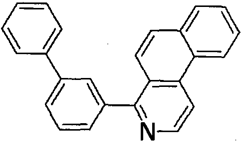
LG-6
[0259]Next, Ir-405 as an iridium complex was synthesized by the same method as that of the section (1-2) of
Synthesis Example 1 except that in the section (1-2) of
Synthesis Example 1, LG-6 was used instead of LG-1 and 2, 2, 6, 6-tetramethylheptane-3, 5-dione was used instead of acetylacetone .
[0260] The structure of Ir-405 thus obtained was confirmed by performing identification in the same manner as in the iridium complex obtained in Synthesis Example 1. In addition, its maximum emission peak wavelength was measured by PL spectrum measurement. The results are shown below.
PL: (Amax=) 616 nm
MS: measured value=1037.39 (calculated value: 1036.36) [0261] [Synthesis Example 10] (Synthesis of Exemplified
Compound Ir-515)
Ir-515 was synthesized according to the following synthesis scheme with reference to, for example, PTL 4.
[0262]

[0263]The structure of Ir-515 thus obtained was confirmed by performing identification in the same manner as in the iridium complex obtained in Synthesis Example 1. In addition, its maximum emission peak wavelength was measured by PL spectrum measurement. The results are shown below.
PL: (Araax=) 623 nm
MS: measured value=1087.34 (calculated value: 1087.35) [0264] [Synthesis Example 11] (Synthesis of Compound H-105) [0265]

[0266] he following reagents and solvent were loaded into a 100-mL recovery flask.
3-Chlorochrysene (CRY-1) : 525 mg (2.00 mmol)
Boronic acid compound (FL-1): 1,017 mg (2.00 mmol) Palladium (II) acetate: 18 mg (80 μηαοΐ)
Dicyclohexyl (2 ' , 6 ' -dimethoxybiphenyl-2-yl ) phosphine : 80 mg (194 μπιοΐ)
Potassium phosphate: 1.06 g (5.00 mmol)
Toluene: 50 mL
[0267]Next, the reaction solution was refluxed by heating for 8 hours while being stirred. After the completion of the reaction, water was added to the resultant, a liquid-separating operation was performed, and an organic layer was recovered. After that, the organic layer was dried. Next, the organic layer was
concentrated under reduced pressure to provide a crude product. After that, the crude product was purified by employing silica gel column chromatography (developing solvent: heptane/toluene=4 /l ) . Next, the purified product was recrystallized with a toluene/ethanol mixed solvent and then the resultant crystal was vacuum-dried at 150°C. Next, sublimation purification was performed to provide 830 mg of Exemplified Compound H-105 (yield: 68%). The resultant compound was evaluated for its purity by employing HPLC. As a result, it was
confirmed that the purity was 99% or more.
[0268] he resultant compound was identified by matrix- assisted laser desorption/ionization time-of-flight mass spectrometry (MALDI-TOF-MS ) with an Autoflex LRF (trade name; manufactured by Bruker) . The result is
shown below.
MS: measured value=612.88 (calculated value
[0269] [Synthesis Example 12] (Synthesis of D-102)
[0270]

[0271] he following reagents and solvent were loaded into a 100-mL recovery flask.
3-Chlorochrysene (CRY-1): 578 mg (2.2 mmol)
Boronic acid compound (NP-1) : 380 mg (1.0 mmol)
Palladium ( II ) acetate: 18 mg (80 μπιοΐ)
Dicyclohexyl (2 ' , 6 ' -dimethoxybiphenyl-2-yl ) phosphine : 80 mg (194 μιτιοΐ)
Potassium phosphate: 1.06 g (5.00 mmol)
Toluene: 50 mL
[0272]Next, the reaction solution was refluxed by heating for 8 hours while being stirred. After the completion of the reaction, water was added to the resultant, a liquid-separating operation was performed, and an organic layer was recovered. After that, the organic layer was dried. Next, the organic layer, was
concentrated under reduced pressure to provide a crude product. After that, the crude product was purified by employing silica gel column chromatography (developing solvent: heptane/toluene= /l ) . Next, the purified product was recrystallized with a toluene/ethanol mixed solvent and then the resultant crystal was vacuum-dried at 150°C. Next, sublimation purification was performed to provide 337 mg of Exemplified Compound D-102 (yield: 58%). The resultant compound was evaluated for its purity by employing HPLC. As a result, it was
confirmed that the purity was 99% or more.
[0273] The resultant compound was identified by the same method as that of Synthesis Example 11. The result is shown below.
MS: measured value=580.43 (calculated value=580.22 ) [0274] [Synthesis Example 13] (Synthesis of Compound F-101) F-101 was obtained by the same method as that of
Synthesis Example 11 except that in Synthesis Example 11, 3-chlorophenanthrene was used instead of 3- chlorochrysene and FL-2 represented below was used instead of FL-1.
[0275]

FL-2
[0276]The resultant compound was identified by the same
method as that of Synthesis Example 11. The result is shown below.
MS: measured value=754.39 (calculated value=755.00 ) [0277] [Synthesis Example 14] (Synthesis of Compound H-102) H-102 was obtained by the same method as that of
Synthesis Example 11 except that in Synthesis Example 11, 3-chlorophenanthrene was used instead of 3- chlorochrysene .
[0278] [Synthesis Example 15] (Synthesis of Compound L-104) L-104 was obtained by the same method as that of
Example 11 except that in Synthesis Example 11, NPTRP-1 represented below was used instead of FL-1.
[0279]

NPTRP-1
[0280] he resultant compound was identified by the same
method as that of Synthesis Example 11. The result shown below.
MS: measured value=580.13 (calculated value=580.22 ) [0281] [Synthesis Example 16] (Synthesis of Compound L-105) [0282]

CRY-2 NPCRY-1 L-105
[0283] (16-1) Synthesis of Intermediate NPCRY-1
The following reagents and solvents were loaded into a 100-mL three-necked flask.
CRY-2: 1.23 g (3.0 mmol)
NP-2: 0.53 g (3.1 mmol)
Tetrakis (triphenylphosphine) palladium (0) : 0.1 g (0.08 mmol )
Toluene: 10 mL
Ethanol: 5 mL
10 wt% aqueous solution of sodium carbonate: 5 mL
[0284]Next, the reaction solution was refluxed by heating for 5 hours while being stirred under nitrogen. After the completion of the reaction, the reaction solution was washed with water, dried over sodium sulfate, and then concentrated under reduced pressure to provide a crude product. Next, the crude product was purified by silica gel column chromatography (developing solvent: toluene/heptane=2/l) to provide 0.99 g (yield: 85%) . of Intermediate NPCRY-1.
[0285] (16-2) Synthesis of Exemplified Compound L-105
The following reagents and solvent were loaded into a 100-mL recovery flask.
Intermediate NPCRY-1: 389 mg (1.0 mmol)
Boronic acid compound TRP-2 : 272 mg (1.0 mmol) Palladium ( II ) acetate: 18 mg (80 mol)
Dicyclohexyl (2 ' , 6 ' -dimethoxybiphenyl-2-yl ) hosphine : 80 mg (194 μιηοΐ)
Potassium phosphate: 0.53 g (2.5 mmol)
Toluene: 10 mL
[0286] Next, the reaction solution was refluxed by heating for 8 hours while being stirred under nitrogen. After the completion of the reaction, water was added to the reaction solution, a liquid-separating operation was performed, and an organic layer was ' recovered. After that, the organic layer was dried. Next, the organic layer was concentrated under reduced pressure to provide a crude product. After that, the crude product was purified by silica gel column chromatography
(developing solvent: heptane/toluene=4 /l ) . After that, the purified product was recrystallized with a
toluene/ethanol mixed solvent and then the resultant crystal was vacuum-dried at 150°C. After that,
sublimation purification was performed to provide 458 mg of Exemplified Compound L-105 (yield: 79%). The resultant compound was evaluated for its purity by employing HPLC. As a result, it was confirmed that the purity was 99% or more.
[0287] The resultant compound was identified by the same
method as that of Synthesis Example 11. The result is shown below.
MS: measured value=580.01 (calculated value=580.22 ) [0288] [Synthesis Example 17] (Synthesis of Compound J-105)
[0289]

Synthesis Example 16 except that in Synthesis Example 16, NP-3 was used instead of CRY-2 and TRP-2 was used instead of NP-2. The result of the identification of the resultant compound is shown below.
[0291] The resultant compound was identified by the same
method as that of Synthesis Example 11. The result is shown below.
MS: measured value=606.88 (calculated value=606.23)
[0292] [Example 1]
In this example, an organic light-emitting device
(anode/hole-inj ecting layer/hole-transporting
layer/emission 1ayer/hoie/exciton-blocking
layer/electron-transporting layer/cathode) described as the fifth example of the multilayer-type organic light- emitting device was produced.
[0293] First, ITO was formed into a film on a glass substrate and then subjected to desired patterning processing by photolithography to form an ITO electrode (anode) . At this time, the thickness of the ITO electrode was set to 100 nm. The substrate on which the ITO electrode had been thus formed was used as an ITO substrate in the following steps.
[ 029 ] Organic compound layers and electrode layers shown in Table 2 below were continuously formed on the ITO substrate. It is to be noted that a vacuum vapor deposition method based on resistance heating in a vacuum chamber having a pressure condition of 1χ10~5 Pa was adopted as a film-forming method. In addition, the electrode area of the opposing electrode (metal
electrode layers, cathode) was set to 3 mm2.
[0295]Table 2
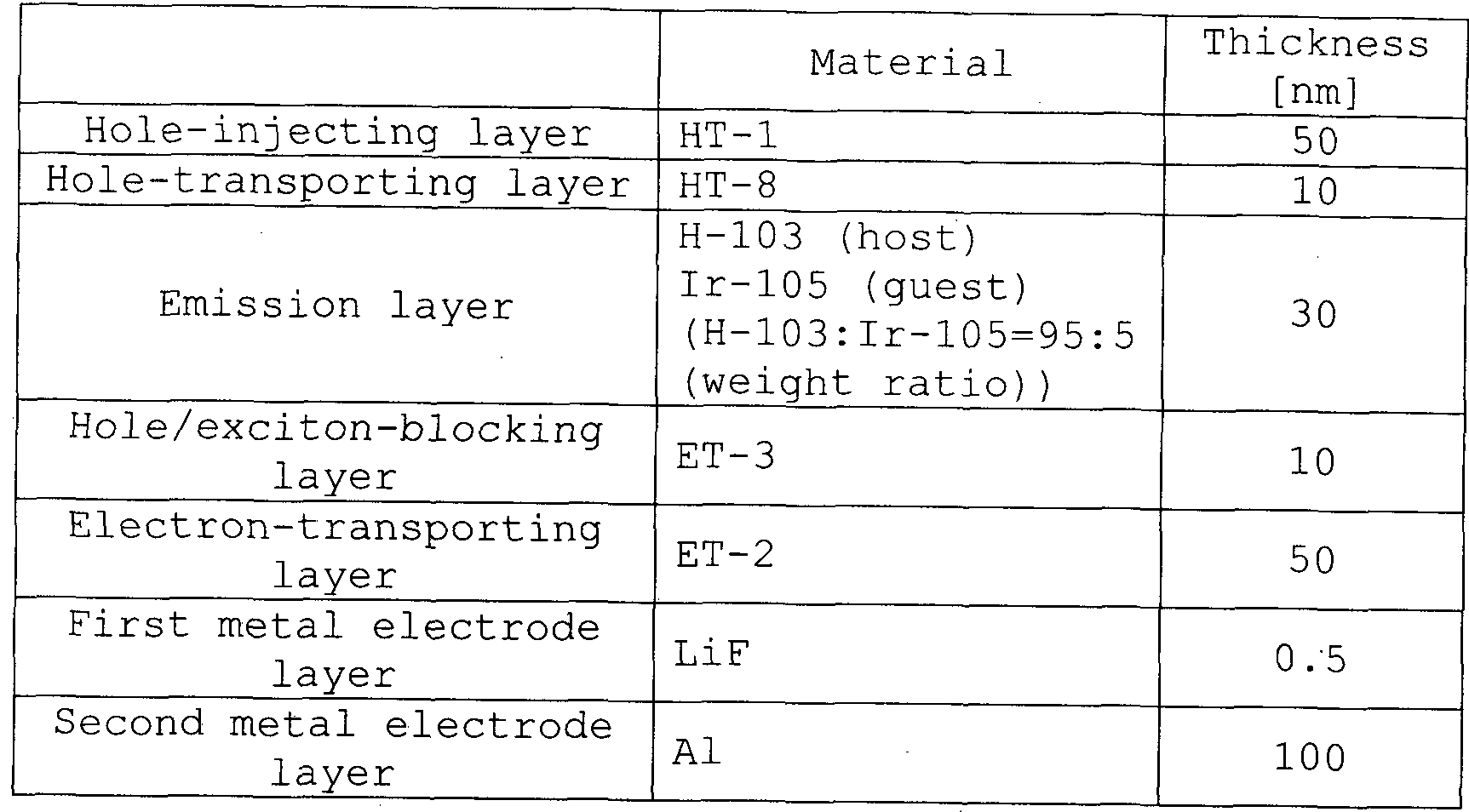
[0296]Next, the produced device was encapsulated with a glass cap with a moisture absorbent in an inert atmosphere to provide an organic light-emitting device.
[0297]The current-voltage characteristics ..of "the resultant organic light-emitting device were measured with an ammeter 2700 (trade name; manufactured by Keithley Instruments, Inc.) and its emission luminance was measured with a BM7-Fast (trade name; manufactured by TOPCON CORPORATION). Table 3 shows the results.
[0298] [Example 2]
An organic light-emitting device was produced by the same method as that of Example 1 except that in Example 1, the host and the guest were changed to B-105 and Ir- 301, respectively. The current-voltage characteristics and emission luminance of the resultant organic light- emitting device were measured in the same manner as in Example 1. Table 3 shows the results.
[0299] [Example 3]
An organic light-emitting device was produced by the same method as that of Example 1 except that in Example 1, the host and the guest were changed to D-102 and Ir-
317, respectively. The current-voltage characteristics and emission luminance of the resultant organic light- emitting device were measured in the same manner as in Example 1. Table 3 shows the results..
[0300] [Example 4]
An organic light-emitting device was produced by the same method as that of Example 1 except that in Example 1, the host and the guest were changed to F-101 and Ir- 206, respectively. The current-voltage characteristics and emission luminance of the resultant organic light- emitting device were measured in the same manner as in Example 1. Table 3 shows the results.
[0301] [Example 5]
An organic light-emitting device was produced by the same method as that of Example 1 except that in Example 1, the host and the guest were changed to H-102 and Ir- 405, respectively. The current-voltage characteristics and emission luminance of the resultant organic light- emitting device were measured in the same manner as in Example 1. Table 3 shows the results.
[0302] [Example 6]
An organic EL device was produced by the same method as that of Example 1 except that in Example 1, the host was changed to J-105. The current-voltage
characteristics and emission luminance of the resultant . organic light-emitting device were measured in the same manner as in Example 1. Table 3 shows the results.
[0303] [Example 7]
An organic light-emitting device was produced by the same method as that of Example 1 except that in Example 1, the host was changed to K-104. The current-voltage characteristics and emission luminance of the resultant organic light-emitting device were measured in the same manner as in Example 1. Table 3 shows the results.
[0304] [Example 8]
An organic light-emitting device was produced by the
same method as that of Example 1 except that in Example 1, the host and the guest were changed to L-104 and Ir- 213, respectively. The current-voltage characteristics and emission luminance of the resultant organic light- emitting device were measured in the same manner as in Example 1. Table 3 shows the results.
[0305] [Example 9]
An organic light-emitting device was produced by the same method as that of Example 1 except that in Example 1, the host was changed to L-105. The current-voltage characteristics and emission luminance of the resultant organic light-emitting device were measured in the same manner as in Example 1. Table 3 shows the results.
[0306] [Example 10]
An organic EL device was produced by the same method as that of Example 1 except that in Example 1, the host and the guest were changed to H-103 and Ir-515, respectively. The current-voltage characteristics and emission luminance of the resultant organic light- emitting device were measured in the same manner as in Example 1. Table 3 shows the results.
[0307] [Example 11]
An organic light-emitting device was produced by the same method as that of Example 1 except that in Example 1, H-103 (host), Ir-206 (guest), and M-103 (third component) were used in the formation of the emission layer, and the emission layer was formed so that a weight ratio among the three components "H-103: Ir- 206:M-103" became 75:5:20. The current-voltage
characteristics and emission luminance of the resultant organic light-emitting device were measured in the same manner as in Example 1. Table 3 shows the results.
[0308] [Example 12]
An organic light-emitting device was produced by the same method as that of Example 1 except that in Example 1, L-104 (host), Ir-316 (guest), and M-105 (third
component) were used in the formation of the emission layer, and the emission layer was formed so that a weight ratio among the three components "L-104 :Ir- 316:M-105" became 75:5:20. The current-voltage
characteristics and emission luminance of the resultant organic light-emitting device were measured in the same manner as in Example 1. Table 3 shows the results.
[0309] [Example 13]
An organic light-emitting device was produced by the same method as that of Example 1 except that in Example 1, L-104 (host), Ir-318 (guest), and N-105 (third component) were used in the formation of the emission layer, and the emission layer was formed so that a weight ratio among the three components "L-104 : Ir- 318:N-105" became 75:5:20. The current-voltage
characteristics and emission luminance of the resultant organic light-emitting device were measured in the same manner as in Example 1. Table 3 shows the results.
[0310] [Example 14]
An organic light-emitting device was produced by the same method as that of Example 1 except that in Example 1, L-105 (host), Ir-318 (guest), and O-101 (third component) were used in the formation of the emission layer, and the emission layer was formed so that a weight ratio among the three components "L-105: Ir- 318 :O-101" became 75:5:20. The current-voltage
characteristics and emission luminance of the resultant organic light-emitting device were measured in the same manner as in Example 1. Table 3 shows the results.
[0311] [Comparative Example 1]
An organic light-emitting device was produced by the same method as that of Example 1 except that in Example 1, 4, 41 -di (9H-carbazol-9-yl) -1, 1 ' -biphenyl (CBP) was used instead of H-103 as the host. The current-voltage characteristics and emission luminance of the resultant organic light-emitting device were measured in the same
manner as in Example 1. Table 3 shows the results.
[0312] [Comparative Example 2]
An organic EL device was produced by the same method as that of Example 2 except that in Example 2 ,
2, 2 ' : 61 , 2 ' ' : 6 ' ' , 2 ' ' ' -quaternaphthalene (NP4) was used instead of B-105 as the host. The current-voltage characteristics and emission luminance of the resultant organic light-emitting device were measured in the same manner as in Example 1. Table 3 shows the results.
[0313]Table 3

[0314] The organic light-emitting devices of Examples have been improved in emission efficiency and luminance half-life as compared with the organic light-emitting devices of Comparative Examples. This may result from the fact that the compound incorporated as the host into the emission layer is formed only of a hydrocarbon and the fact that the structure of the compound serving as the host is not linear.
[ 0315 ] Further, in each of Examples 11 to 14, the emission efficiency or the luminance half-life has been
additionally improved by further incorporating the
material except the host and the guest (third component) into the emission layer. This may result from the fact that the following was able to be
avoided: the benzo [f] isoquinoline skeleton in the complex serving as the guest was brought into a radical state.
[0316] [Example 15]
A top emission-type organic light-emitting device was produced by a method described below.
[0317] First, Al was formed into a film on a glass substrate (transparent substrate) by a sputtering method to form an Al layer. Next, an indium zinc oxide was formed into a film on the Al layer by the sputtering method to form a transparent electrode layer. At this time, the thickness of the transparent electrode layer was set to 80 nm. Next, an acrylic resin was formed into a film on the transparent electrode layer and then patterning was performed by employing a photolithography process. Thus, a pixel separation film was obtained. At this time, a laminated electrode layer. formed by laminating the Al layer and the transparent electrode layer in the stated order was divided by the pixel separation film, and an electrode area per one pixel was 3 mm2. Thus, a substrate with an electrode was obtained.
[ 0318 ] Organic compound layers and electrode layers shown in Table 4 below were continuously formed on the ITO substrate. It is to be noted that a vacuum vapor deposition method based on resistance heating in a vacuum chamber having a pressure condition of 1*10"5 Pa was adopted as a film-forming method.
[0319] Table 4

[0320] ext, the produced device was encapsulated with a glass cap with a moisture absorbent in an inert atmosphere to provide an organic light-emitting device.
[0321] he emission efficiency of the resultant organic light- emitting device was measured and evaluated in the same manner as in Example 1. As . a result, the emission efficiency was 40 cd/A.
[0322] The foregoing shows that the organic compound
represented by the general formula [5] or [10] is a host that provides high emission efficiency, and the compound can improve the light-emitting characteristics (such as emission efficiency) of an organic light- emitting device when used in the device together with the iridium complex represented by the general formula [1] ([6]).
[0323]As described above with reference, to the embodiments and Examples, according to the present invention, it is possible to provide the organic light-emitting device improved in emission efficiency and lifetime.
[0324]While the present invention has been described with
reference to exemplary embodiments, it is to be
understood that the invention is not limited to the
disclosed exemplary embodiments. The scope of the following claims is to be accorded the broadest interpretation so as to encompass all such
modifications and equivalent structures and functions. his application claims the benefit of Japanese Patent Application No. 2012-285620, filed December 27, 2012, and Japanese Patent Application No. 2013-264147, filed December 20, 2013, which are hereby incorporated by reference herein in their entirety.
Claims
An organic light-emitting device, comprising:
a pair of electrodes; and
an organic compound layer disposed between the pair of electrodes ,
wherein :
the organic compound layer includes an iridium complex represented by the following general formula [1] and a hydrocarbon compound represented by the following general formula [5] ; and
the hydrocarbon compound comprises a compound formed only of an SP2 carbon atom and a hydrogen atom:

in the formula [1] :
Ri to R8 each represent a hydrogen atom, a halogen atom, an alkyl group, an alkoxy group, a trifluoromethyl group, a cyano group, a substituted or unsubstituted aromatic hydrocarbon group, or a substituted or
unsubstituted heteroaromatic group;
m represents an integer of 1 to 3 and n represents an integer of 0 to 2, provided that m+n equals 3;
a ring A represents a cyclic structure selected from a benzene ring, a naphthalene ring, a fluorene ring, a phenanthrene ring, a 9 , 9-spirobifluorene ring, and. a chrysene ring, and is covalently bonded to a
benzo [ f ] isoquinoline skeleton and an Ir metal, and the ring A may further have a substituent;
X represents a bidentate ligand; and
a partial structure IrXn comprises any one of
structures represented by the following general

in the formulae [2] to [4], Ri0 to R24 each represent a hydrogen atom, a halogen atom, an alkyl group, an alkoxy group, a trifluoromethyl group, a cyano group, a substituted or unsubstituted aromatic hydrocarbon group or a substituted or unsubstituted heteroaromatic group;
(Ar2)p-(Ar3)q— Art 15]
in the formula [5] :
p and q each represent 0 or 1, and p+q is equal to or more than 1;
Ari represents any one of substituents represented in the following substituent group a; and
Ar2 and Ar3 each represent any one of substituents represented in the following substituent group β, and
Ar2 and Ar3 may be identical to or different from each other.
[Substituent roup a]

[Substituent group
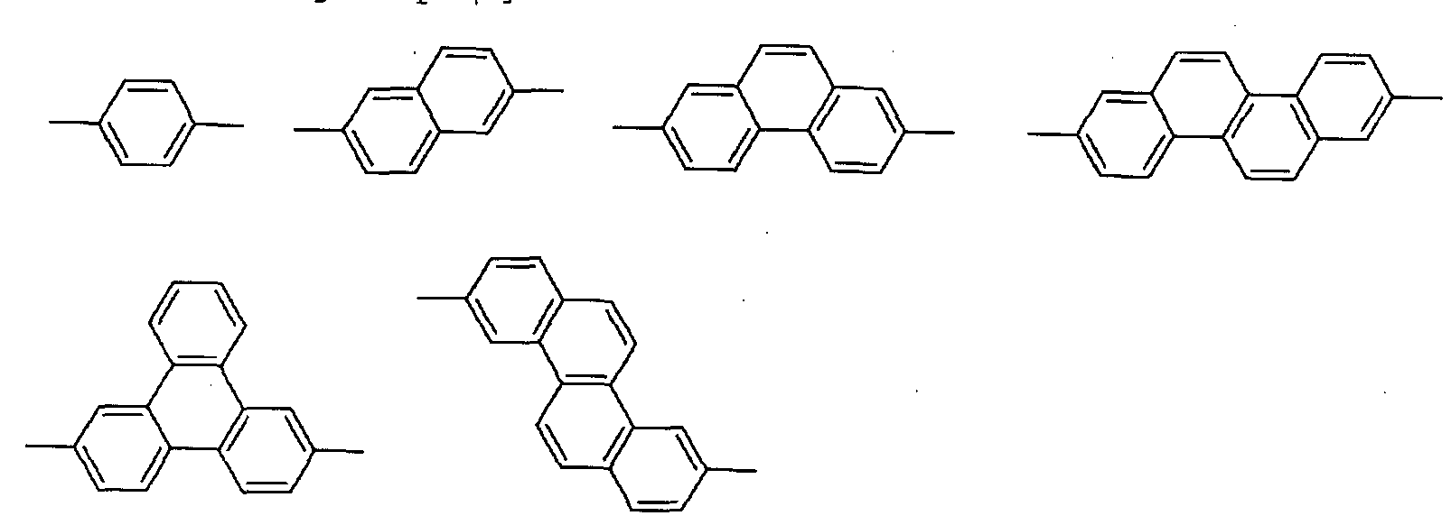
[2] An organic light-emitting device, comprising:
a pair of electrodes; and
an organic compound layer disposed between the pair of electrodes,
wherein the organic compound layer includes an iridium complex represented by the following general formula [6] and a hydrocarbon compound represented by the following general formula [10]:

in the formula [6] :
R31 to R38 each represent a hydrogen atom, a halogen atom, an alkyl group, an alkoxy group, a
trifluoromethyl group, a cyano group, a substituted or unsubstituted aromatic hydrocarbon group, or a
substituted or unsubstituted heteroaromatic group;
k represents an integer of 1 to 3 and 1 represents an integer of 0 to 2, provided that k+1 equals 3;
a ring A represents a cyclic structure selected from a benzene ring, a naphthalene ring, a fluorene ring, a phenanthrene ring, a 9, 9-spirobifluorene ring, and a chrysene ring, and is covalently bonded to a
benzo [ f] isoquinoline skeleton and an Ir metal, and the ring A may further have a substituent ;
X represents a bidentate ligand; and
a partial structure IrXi comprises any one of
structures represented by the following general formulae [7] to [9] :

in the formulae [7] to [9], R39 to R53 each represent a hydrogen atom, a halogen atom, an alkyl group, an alkoxy group, a trifluoromethyl group, a cyano group, a
substituted or unsubstituted aromatic hydrocarbon group, or a substituted or unsubstituted heteroaromatic group; Ar5- (Ar6) r- (Ar7) S-Ar8 [10]
in the formula [10] :
r and s each represent 0 or 1, and r+s is equal to or more than 1;
Ar5 represents any one of substituents represented in the following substituent group a' ;
Ar6 and Ar7 each represent any one of substituents represented in the following substituent group β' , and Ar6 and Ar7 may be identical to or different from each other; and
Ar8 represents any one of substituents represented in the following substituent group γ' .
Substituent group α']

SP2 carbon atom and a hydrogen atom.
[4] An organic light-emitting device according to any one of claims 1 to 3, wherein the m or k represents 2 and the n or 1 represents 1.
[5] An organic light-emitting device according to any one of claims 1 to 4, wherein the iridium complex is represented by the following formula [11]:

in the formula [11] :
R6i to R7i each represent a hydrogen atom, a halogen atom, an alkyl group, an alkoxy group, a
trifluoromethyl group, a cyano group, a substituted or unsubstituted aromatic hydrocarbon group, or a
substituted or unsubstituted heteroaromatic group; t represents an integer of 1 to 3 and u represents an integer of 0 to 2, provided that t+u equals 3;
*1 represents a bond between the ring A and the Ir metal, and *2 represents a bond between the ring A and a carbon atom at a 1-position in the
benzo [f] isoquinoline skeleton; and
the ring A comprises any one of structures represented by the following general formulae [12] to [16]:

in the formulae [12] to [16]:
R.72 to R93 each represent a hydrogen atom, a halogen atom, an alkyl group, an alkoxy group, a
trifluoromethyl group, a cyano group, a substituted or unsubstituted aromatic hydrocarbon group, or a
substituted or unsubstituted heteroaromatic group; and *1 represents a bonding position with the Ir metal and * 2 represents a bonding position with the carbon atom at the 1-position in the benzo [f ] isoquinoline skeleton. An organic light-emitting device according to claim 5, wherein the ring A comprises the structure represented by the general formula [12].
An organic light-emitting device according to any one of claims 1 to 6, wherein the iridium complex comprises an iridium complex represented by the following general formula [ 17 ] :

in the formula [17]:
Qi to Qg each represent a hydrogen atom, a halogen atom, an alkyl group, an alkoxy group, a trifluoromethyl group, or a cyano group; and
G represents a hydrogen atom, a halogen atom, an alkyl group, an alkoxy group, a trifluoromethyl group, a cyano group, or a substituted or unsubstituted phenyl group .
[8] An organic light-emitting device according to any one of claims 1 to 7, wherein the organic compound layer is formed of the iridium complex, the hydrocarbon compound, and a third component.
[9] An organic light-emitting device according to claim 8, wherein a highest occupied molecular orbital (HOMO) level of the third component is higher than an HOMO of the hydrocarbon compound.
[10] An organic light-emitting device according to claim 8 or 9, wherein a lowest unoccupied molecular orbital (LUMO) level of the third component is higher than an LUMO of the hydrocarbon compound.
[11] A display apparatus, comprising multiple pixels,
wherein the pixels each have the organic light-emitting device according to any one of claims 1 to 10 and a transistor connected to the organic light-emitting device .
[12] A display apparatus according to claim 11, wherein the
transistor includes an electrode formed of a transparent oxide semiconductor.
[13] A display apparatus according to claim 11 or 12,
further comprising a color filter.
[14] A display apparatus, which is formed by laminating the organic light-emitting device according to any one of claims 1 to 10, to thereby output white light.
Priority Applications (3)
| Application Number | Priority Date | Filing Date | Title |
|---|---|---|---|
| EP13868746.2A EP2939288B1 (en) | 2012-12-27 | 2013-12-25 | Organic light-emitting device and display apparatus |
| US14/648,095 US9960370B2 (en) | 2012-12-27 | 2013-12-25 | Organic light-emitting device and display apparatus |
| CN201380067403.1A CN104885248B (en) | 2012-12-27 | 2013-12-25 | Organic light-emitting device and display apparatus |
Applications Claiming Priority (4)
| Application Number | Priority Date | Filing Date | Title |
|---|---|---|---|
| JP2012285620 | 2012-12-27 | ||
| JP2012-285620 | 2012-12-27 | ||
| JP2013-264147 | 2013-12-20 | ||
| JP2013264147A JP5818870B2 (en) | 2012-12-27 | 2013-12-20 | Organic light emitting device and display device |
Publications (1)
| Publication Number | Publication Date |
|---|---|
| WO2014104395A1 true WO2014104395A1 (en) | 2014-07-03 |
Family
ID=51021450
Family Applications (1)
| Application Number | Title | Priority Date | Filing Date |
|---|---|---|---|
| PCT/JP2013/085323 WO2014104395A1 (en) | 2012-12-27 | 2013-12-25 | Organic light-emitting device and display apparatus |
Country Status (5)
| Country | Link |
|---|---|
| US (1) | US9960370B2 (en) |
| EP (1) | EP2939288B1 (en) |
| JP (1) | JP5818870B2 (en) |
| CN (1) | CN104885248B (en) |
| WO (1) | WO2014104395A1 (en) |
Cited By (8)
| Publication number | Priority date | Publication date | Assignee | Title |
|---|---|---|---|---|
| US9484541B2 (en) | 2014-10-20 | 2016-11-01 | Universal Display Corporation | Organic electroluminescent materials and devices |
| US20180130956A1 (en) * | 2016-11-09 | 2018-05-10 | Universal Display Corporation | Organic electroluminescent materials and devices |
| EP3715354A1 (en) * | 2019-03-29 | 2020-09-30 | Samsung Electronics Co., Ltd. | Organometallic compound, organic light-emitting device including organometallic compound, and diagnostic composition including organometallic compound |
| EP3892705A1 (en) * | 2020-04-09 | 2021-10-13 | Canon Kabushiki Kaisha | Iridium complex-containing composition, organic light emitting device having the same, display apparatus, imaging apparatus, electronic equipment, lighting apparatus, and moving body |
| US11342509B2 (en) | 2018-02-09 | 2022-05-24 | Universal Display Corporation | Organic electroluminescent materials and devices |
| US11800788B2 (en) | 2018-12-28 | 2023-10-24 | Samsung Electronics Co., Ltd. | Organometallic compound and organic light-emitting device including i he same |
| US12063850B2 (en) | 2019-12-24 | 2024-08-13 | Samsung Electronics Co., Ltd. | Organometallic compound, organic light-emitting device including the same and electronic apparatus including the organic light-emitting device |
| US12075692B2 (en) | 2020-05-15 | 2024-08-27 | Canon Kabushiki Kaisha | Iridium complex-containing composition, organic light emitting device having the same, display apparatus, imaging apparatus, electronic equipment, lighting apparatus, and moving body |
Families Citing this family (13)
| Publication number | Priority date | Publication date | Assignee | Title |
|---|---|---|---|---|
| JP5984689B2 (en) * | 2013-01-21 | 2016-09-06 | キヤノン株式会社 | Organometallic complex and organic light emitting device using the same |
| CN104076564A (en) * | 2014-06-09 | 2014-10-01 | 京东方科技集团股份有限公司 | Array substrate, preparation method for same, and display device |
| JP6552201B2 (en) | 2015-01-19 | 2019-07-31 | キヤノン株式会社 | Organic light emitting device |
| JP2018160548A (en) * | 2017-03-22 | 2018-10-11 | 東芝メモリ株式会社 | Storage device and rectifying device |
| EP3637489A1 (en) * | 2018-10-08 | 2020-04-15 | Samsung Electronics Co., Ltd. | Organometallic compound and organic light-emitting device including the same |
| US11760769B2 (en) * | 2019-03-29 | 2023-09-19 | Samsung Electronics Co., Ltd. | Composition and organic light-emitting device including the same |
| US11758802B2 (en) * | 2019-03-29 | 2023-09-12 | Samsung Electronics Co., Ltd. | Composition and organic light-emitting device including the same |
| CN112592371A (en) * | 2019-10-02 | 2021-04-02 | 环球展览公司 | Organic electroluminescent material and device |
| KR20210079766A (en) * | 2019-12-20 | 2021-06-30 | 삼성전자주식회사 | Organometallic compound and organic light emitting device including the same |
| US20220352476A1 (en) * | 2020-02-28 | 2022-11-03 | Universal Display Corporation | Organic electroluminescent materials and devices |
| CN113387983B (en) * | 2020-03-11 | 2023-04-18 | 北京夏禾科技有限公司 | Metal complex of ligand with polysubstituted biaryl structure |
| KR20230126112A (en) * | 2022-02-22 | 2023-08-29 | 삼성전자주식회사 | Organic light emitting device and electronic apparatus including the same |
| JP2024003550A (en) * | 2022-06-27 | 2024-01-15 | キヤノン株式会社 | Organic light emitting element and display device using the same |
Citations (6)
| Publication number | Priority date | Publication date | Assignee | Title |
|---|---|---|---|---|
| JP2005071983A (en) | 2003-08-04 | 2005-03-17 | Fuji Photo Film Co Ltd | Organic electroluminescent device |
| WO2008062129A1 (en) | 2006-11-23 | 2008-05-29 | Essilor International (Compagnie Générale d'Optique) | Opto-electronic display assembly |
| WO2009060995A1 (en) * | 2007-11-08 | 2009-05-14 | Canon Kabushiki Kaisha | Organic metal complex, and organic light emitting device and display apparatus using the same |
| JP2009130141A (en) * | 2007-11-22 | 2009-06-11 | Idemitsu Kosan Co Ltd | Organic el device and solution containing organic el material |
| US20090174313A1 (en) * | 2007-11-22 | 2009-07-09 | Idemitsu Kosan Co., Ltd. | Organic electroluminescence device and organic-electroluminescence-material-containing solution |
| WO2010028151A1 (en) | 2008-09-03 | 2010-03-11 | Universal Display Corporation | Phosphorescent materials |
Family Cites Families (22)
| Publication number | Priority date | Publication date | Assignee | Title |
|---|---|---|---|---|
| JP2003007469A (en) | 2001-06-25 | 2003-01-10 | Canon Inc | Light emitting element and display equipment |
| JP3919583B2 (en) | 2002-04-12 | 2007-05-30 | キヤノン株式会社 | Organic light emitting device |
| JP4478555B2 (en) | 2004-11-30 | 2010-06-09 | キヤノン株式会社 | Metal complex, light emitting element and image display device |
| KR101634423B1 (en) * | 2005-05-31 | 2016-06-28 | 유니버셜 디스플레이 코포레이션 | Triphenylene hosts in phosphorescent light emitting diodes |
| JP5127206B2 (en) | 2006-11-28 | 2013-01-23 | キヤノン株式会社 | Metal complex compound, organic light emitting device and display device |
| WO2009008201A1 (en) * | 2007-07-07 | 2009-01-15 | Idemitsu Kosan Co., Ltd. | Naphthalene derivative, material for organic el element, and organic el element using the material |
| EP2166592A4 (en) * | 2007-07-07 | 2012-04-18 | Idemitsu Kosan Co | Organic el device |
| US8211552B2 (en) * | 2007-07-07 | 2012-07-03 | Idemitsu Kosan Co., Ltd. | Organic electroluminescence device |
| KR100910153B1 (en) | 2007-11-20 | 2009-07-30 | (주)그라쎌 | Novel red electroluminescent compounds and organic electroluminescent device using the same |
| US8574725B2 (en) * | 2007-11-22 | 2013-11-05 | Idemitsu Kosan Co., Ltd. | Organic el element and solution containing organic el material |
| CN101945839A (en) * | 2007-12-21 | 2011-01-12 | 住友化学株式会社 | The preparation method of conjugation aromatic substance |
| JP5618495B2 (en) * | 2008-05-16 | 2014-11-05 | キヤノン株式会社 | Organic light emitting device |
| JP2010114070A (en) * | 2008-10-10 | 2010-05-20 | Canon Inc | White organic el element |
| TWI541234B (en) * | 2009-05-12 | 2016-07-11 | 環球展覽公司 | 2-azatriphenylene materials for organic light emitting diodes |
| US20100295027A1 (en) | 2009-05-22 | 2010-11-25 | Idemitsu Kosan Co., Ltd. | Organic electroluminescence device |
| JP5770441B2 (en) * | 2009-09-30 | 2015-08-26 | ユー・ディー・シー アイルランド リミテッド | Material for organic electroluminescence device and organic electroluminescence device |
| JP4617393B1 (en) * | 2010-01-15 | 2011-01-26 | 富士フイルム株式会社 | Organic electroluminescence device |
| JP5047314B2 (en) * | 2010-01-15 | 2012-10-10 | 富士フイルム株式会社 | Organic electroluminescence device |
| JP2011151116A (en) | 2010-01-20 | 2011-08-04 | Canon Inc | Organic light-emitting device |
| TWI428312B (en) * | 2010-10-29 | 2014-03-01 | Nat Univ Tsing Hua | 9,10-bisphenylphenanthrene derivative and organic light emitting diode using the same |
| JP5653179B2 (en) | 2010-11-05 | 2015-01-14 | キヤノン株式会社 | Phenanthrene compound and organic light emitting device using the same |
| BR112013019503B1 (en) * | 2011-02-09 | 2021-05-25 | F. Hoffmann-La Roche Ag | iridium-based chemiluminescent compound, conjugate, uses of a compound and method for measuring an analyte |
-
2013
- 2013-12-20 JP JP2013264147A patent/JP5818870B2/en active Active
- 2013-12-25 CN CN201380067403.1A patent/CN104885248B/en active Active
- 2013-12-25 EP EP13868746.2A patent/EP2939288B1/en active Active
- 2013-12-25 WO PCT/JP2013/085323 patent/WO2014104395A1/en active Application Filing
- 2013-12-25 US US14/648,095 patent/US9960370B2/en active Active
Patent Citations (7)
| Publication number | Priority date | Publication date | Assignee | Title |
|---|---|---|---|---|
| JP2005071983A (en) | 2003-08-04 | 2005-03-17 | Fuji Photo Film Co Ltd | Organic electroluminescent device |
| WO2008062129A1 (en) | 2006-11-23 | 2008-05-29 | Essilor International (Compagnie Générale d'Optique) | Opto-electronic display assembly |
| WO2009060995A1 (en) * | 2007-11-08 | 2009-05-14 | Canon Kabushiki Kaisha | Organic metal complex, and organic light emitting device and display apparatus using the same |
| JP2009114137A (en) | 2007-11-08 | 2009-05-28 | Canon Inc | Organometallic complex, and organic light-emitting element and display apparatus using the same |
| JP2009130141A (en) * | 2007-11-22 | 2009-06-11 | Idemitsu Kosan Co Ltd | Organic el device and solution containing organic el material |
| US20090174313A1 (en) * | 2007-11-22 | 2009-07-09 | Idemitsu Kosan Co., Ltd. | Organic electroluminescence device and organic-electroluminescence-material-containing solution |
| WO2010028151A1 (en) | 2008-09-03 | 2010-03-11 | Universal Display Corporation | Phosphorescent materials |
Non-Patent Citations (2)
| Title |
|---|
| ACCOUNTS OF CHEMICAL RESEARCH, vol. 36, no. 4, 2003, pages 255 |
| See also references of EP2939288A4 |
Cited By (10)
| Publication number | Priority date | Publication date | Assignee | Title |
|---|---|---|---|---|
| US9484541B2 (en) | 2014-10-20 | 2016-11-01 | Universal Display Corporation | Organic electroluminescent materials and devices |
| US20180130956A1 (en) * | 2016-11-09 | 2018-05-10 | Universal Display Corporation | Organic electroluminescent materials and devices |
| US11342509B2 (en) | 2018-02-09 | 2022-05-24 | Universal Display Corporation | Organic electroluminescent materials and devices |
| US11800788B2 (en) | 2018-12-28 | 2023-10-24 | Samsung Electronics Co., Ltd. | Organometallic compound and organic light-emitting device including i he same |
| EP3715354A1 (en) * | 2019-03-29 | 2020-09-30 | Samsung Electronics Co., Ltd. | Organometallic compound, organic light-emitting device including organometallic compound, and diagnostic composition including organometallic compound |
| US11773123B2 (en) | 2019-03-29 | 2023-10-03 | Samsung Electronics Co., Ltd. | Organometallic compound, organic light-emitting device including organometallic compound, and diagnostic composition including organometallic compound |
| US12063850B2 (en) | 2019-12-24 | 2024-08-13 | Samsung Electronics Co., Ltd. | Organometallic compound, organic light-emitting device including the same and electronic apparatus including the organic light-emitting device |
| EP3892705A1 (en) * | 2020-04-09 | 2021-10-13 | Canon Kabushiki Kaisha | Iridium complex-containing composition, organic light emitting device having the same, display apparatus, imaging apparatus, electronic equipment, lighting apparatus, and moving body |
| EP4159828A1 (en) * | 2020-04-09 | 2023-04-05 | Canon Kabushiki Kaisha | Methods of manufacturing a iridium complex-containing composition and an organic light emitting device having such a composition |
| US12075692B2 (en) | 2020-05-15 | 2024-08-27 | Canon Kabushiki Kaisha | Iridium complex-containing composition, organic light emitting device having the same, display apparatus, imaging apparatus, electronic equipment, lighting apparatus, and moving body |
Also Published As
| Publication number | Publication date |
|---|---|
| US20150303386A1 (en) | 2015-10-22 |
| JP2014143405A (en) | 2014-08-07 |
| EP2939288A1 (en) | 2015-11-04 |
| CN104885248B (en) | 2017-04-12 |
| JP5818870B2 (en) | 2015-11-18 |
| EP2939288B1 (en) | 2019-11-06 |
| US9960370B2 (en) | 2018-05-01 |
| CN104885248A (en) | 2015-09-02 |
| EP2939288A4 (en) | 2016-10-26 |
Similar Documents
| Publication | Publication Date | Title |
|---|---|---|
| EP2939288B1 (en) | Organic light-emitting device and display apparatus | |
| EP2945958B1 (en) | Organometallic complex and organic light-emitting element using the complex | |
| EP2939289B1 (en) | Organic light-emitting element | |
| EP2948465B1 (en) | Iridium complex and organic light-emitting device including the same | |
| EP2939287B1 (en) | Organic light-emitting element and display apparatus | |
| CN109196075B (en) | Compound for organic photoelectric device, composition for organic photoelectric device, and display device | |
| JP6222931B2 (en) | Organic light emitting device | |
| KR20130094222A (en) | Light-emitting device material and light-emitting device | |
| EP2954571A1 (en) | Organic light-emitting device | |
| KR102015146B1 (en) | Compounds having bipyridyl group and carbazole ring, and organic electroluminescent element | |
| KR20130024915A (en) | Novel m-terphenyl compound and organic light emitting device including the same | |
| CN107868035B (en) | Compound for organic photoelectric device, composition for organic photoelectric device, and display device | |
| WO2011102102A1 (en) | Novel organic compound and organic light-emitting device | |
| KR20190132632A (en) | Compounds, electronic devices containing them, organic thin film light emitting elements, display devices, and lighting devices | |
| CN117377670A (en) | Compound and organic light emitting device comprising the same | |
| CN118234722A (en) | Compound and organic light emitting device comprising the same |
Legal Events
| Date | Code | Title | Description |
|---|---|---|---|
| 121 | Ep: the epo has been informed by wipo that ep was designated in this application |
Ref document number: 13868746 Country of ref document: EP Kind code of ref document: A1 |
|
| WWE | Wipo information: entry into national phase |
Ref document number: 14648095 Country of ref document: US |
|
| WWE | Wipo information: entry into national phase |
Ref document number: 2013868746 Country of ref document: EP |
|
| NENP | Non-entry into the national phase |
Ref country code: DE |