WO2014103489A1 - 特性の異なる複数種類のキャッシュメモリを有する情報処理装置 - Google Patents
特性の異なる複数種類のキャッシュメモリを有する情報処理装置 Download PDFInfo
- Publication number
- WO2014103489A1 WO2014103489A1 PCT/JP2013/078731 JP2013078731W WO2014103489A1 WO 2014103489 A1 WO2014103489 A1 WO 2014103489A1 JP 2013078731 W JP2013078731 W JP 2013078731W WO 2014103489 A1 WO2014103489 A1 WO 2014103489A1
- Authority
- WO
- WIPO (PCT)
- Prior art keywords
- data
- cache
- memory
- segment
- ram
- Prior art date
- Legal status (The legal status is an assumption and is not a legal conclusion. Google has not performed a legal analysis and makes no representation as to the accuracy of the status listed.)
- Ceased
Links
Images
















Classifications
-
- G—PHYSICS
- G06—COMPUTING OR CALCULATING; COUNTING
- G06F—ELECTRIC DIGITAL DATA PROCESSING
- G06F12/00—Accessing, addressing or allocating within memory systems or architectures
- G06F12/02—Addressing or allocation; Relocation
- G06F12/08—Addressing or allocation; Relocation in hierarchically structured memory systems, e.g. virtual memory systems
- G06F12/0802—Addressing of a memory level in which the access to the desired data or data block requires associative addressing means, e.g. caches
- G06F12/0893—Caches characterised by their organisation or structure
- G06F12/0895—Caches characterised by their organisation or structure of parts of caches, e.g. directory or tag array
-
- G—PHYSICS
- G06—COMPUTING OR CALCULATING; COUNTING
- G06F—ELECTRIC DIGITAL DATA PROCESSING
- G06F12/00—Accessing, addressing or allocating within memory systems or architectures
- G06F12/02—Addressing or allocation; Relocation
- G06F12/08—Addressing or allocation; Relocation in hierarchically structured memory systems, e.g. virtual memory systems
- G06F12/0802—Addressing of a memory level in which the access to the desired data or data block requires associative addressing means, e.g. caches
- G06F12/0866—Addressing of a memory level in which the access to the desired data or data block requires associative addressing means, e.g. caches for peripheral storage systems, e.g. disk cache
-
- G—PHYSICS
- G06—COMPUTING OR CALCULATING; COUNTING
- G06F—ELECTRIC DIGITAL DATA PROCESSING
- G06F12/00—Accessing, addressing or allocating within memory systems or architectures
- G06F12/02—Addressing or allocation; Relocation
- G06F12/08—Addressing or allocation; Relocation in hierarchically structured memory systems, e.g. virtual memory systems
- G06F12/0802—Addressing of a memory level in which the access to the desired data or data block requires associative addressing means, e.g. caches
- G06F12/0806—Multiuser, multiprocessor or multiprocessing cache systems
- G06F12/0813—Multiuser, multiprocessor or multiprocessing cache systems with a network or matrix configuration
-
- G—PHYSICS
- G06—COMPUTING OR CALCULATING; COUNTING
- G06F—ELECTRIC DIGITAL DATA PROCESSING
- G06F12/00—Accessing, addressing or allocating within memory systems or architectures
- G06F12/02—Addressing or allocation; Relocation
- G06F12/08—Addressing or allocation; Relocation in hierarchically structured memory systems, e.g. virtual memory systems
- G06F12/0802—Addressing of a memory level in which the access to the desired data or data block requires associative addressing means, e.g. caches
- G06F12/0866—Addressing of a memory level in which the access to the desired data or data block requires associative addressing means, e.g. caches for peripheral storage systems, e.g. disk cache
- G06F12/0871—Allocation or management of cache space
-
- G—PHYSICS
- G06—COMPUTING OR CALCULATING; COUNTING
- G06F—ELECTRIC DIGITAL DATA PROCESSING
- G06F3/00—Input arrangements for transferring data to be processed into a form capable of being handled by the computer; Output arrangements for transferring data from processing unit to output unit, e.g. interface arrangements
- G06F3/06—Digital input from, or digital output to, record carriers, e.g. RAID, emulated record carriers or networked record carriers
- G06F3/0601—Interfaces specially adapted for storage systems
- G06F3/0602—Interfaces specially adapted for storage systems specifically adapted to achieve a particular effect
- G06F3/061—Improving I/O performance
-
- G—PHYSICS
- G06—COMPUTING OR CALCULATING; COUNTING
- G06F—ELECTRIC DIGITAL DATA PROCESSING
- G06F3/00—Input arrangements for transferring data to be processed into a form capable of being handled by the computer; Output arrangements for transferring data from processing unit to output unit, e.g. interface arrangements
- G06F3/06—Digital input from, or digital output to, record carriers, e.g. RAID, emulated record carriers or networked record carriers
- G06F3/0601—Interfaces specially adapted for storage systems
- G06F3/0602—Interfaces specially adapted for storage systems specifically adapted to achieve a particular effect
- G06F3/061—Improving I/O performance
- G06F3/0611—Improving I/O performance in relation to response time
-
- G—PHYSICS
- G06—COMPUTING OR CALCULATING; COUNTING
- G06F—ELECTRIC DIGITAL DATA PROCESSING
- G06F3/00—Input arrangements for transferring data to be processed into a form capable of being handled by the computer; Output arrangements for transferring data from processing unit to output unit, e.g. interface arrangements
- G06F3/06—Digital input from, or digital output to, record carriers, e.g. RAID, emulated record carriers or networked record carriers
- G06F3/0601—Interfaces specially adapted for storage systems
- G06F3/0628—Interfaces specially adapted for storage systems making use of a particular technique
- G06F3/0655—Vertical data movement, i.e. input-output transfer; data movement between one or more hosts and one or more storage devices
-
- G—PHYSICS
- G06—COMPUTING OR CALCULATING; COUNTING
- G06F—ELECTRIC DIGITAL DATA PROCESSING
- G06F3/00—Input arrangements for transferring data to be processed into a form capable of being handled by the computer; Output arrangements for transferring data from processing unit to output unit, e.g. interface arrangements
- G06F3/06—Digital input from, or digital output to, record carriers, e.g. RAID, emulated record carriers or networked record carriers
- G06F3/0601—Interfaces specially adapted for storage systems
- G06F3/0628—Interfaces specially adapted for storage systems making use of a particular technique
- G06F3/0655—Vertical data movement, i.e. input-output transfer; data movement between one or more hosts and one or more storage devices
- G06F3/0656—Data buffering arrangements
-
- G—PHYSICS
- G06—COMPUTING OR CALCULATING; COUNTING
- G06F—ELECTRIC DIGITAL DATA PROCESSING
- G06F3/00—Input arrangements for transferring data to be processed into a form capable of being handled by the computer; Output arrangements for transferring data from processing unit to output unit, e.g. interface arrangements
- G06F3/06—Digital input from, or digital output to, record carriers, e.g. RAID, emulated record carriers or networked record carriers
- G06F3/0601—Interfaces specially adapted for storage systems
- G06F3/0628—Interfaces specially adapted for storage systems making use of a particular technique
- G06F3/0655—Vertical data movement, i.e. input-output transfer; data movement between one or more hosts and one or more storage devices
- G06F3/0659—Command handling arrangements, e.g. command buffers, queues, command scheduling
-
- G—PHYSICS
- G06—COMPUTING OR CALCULATING; COUNTING
- G06F—ELECTRIC DIGITAL DATA PROCESSING
- G06F3/00—Input arrangements for transferring data to be processed into a form capable of being handled by the computer; Output arrangements for transferring data from processing unit to output unit, e.g. interface arrangements
- G06F3/06—Digital input from, or digital output to, record carriers, e.g. RAID, emulated record carriers or networked record carriers
- G06F3/0601—Interfaces specially adapted for storage systems
- G06F3/0668—Interfaces specially adapted for storage systems adopting a particular infrastructure
- G06F3/067—Distributed or networked storage systems, e.g. storage area networks [SAN], network attached storage [NAS]
-
- G—PHYSICS
- G06—COMPUTING OR CALCULATING; COUNTING
- G06F—ELECTRIC DIGITAL DATA PROCESSING
- G06F3/00—Input arrangements for transferring data to be processed into a form capable of being handled by the computer; Output arrangements for transferring data from processing unit to output unit, e.g. interface arrangements
- G06F3/06—Digital input from, or digital output to, record carriers, e.g. RAID, emulated record carriers or networked record carriers
- G06F3/0601—Interfaces specially adapted for storage systems
- G06F3/0668—Interfaces specially adapted for storage systems adopting a particular infrastructure
- G06F3/0671—In-line storage system
- G06F3/0673—Single storage device
- G06F3/068—Hybrid storage device
-
- G—PHYSICS
- G06—COMPUTING OR CALCULATING; COUNTING
- G06F—ELECTRIC DIGITAL DATA PROCESSING
- G06F2212/00—Indexing scheme relating to accessing, addressing or allocation within memory systems or architectures
- G06F2212/10—Providing a specific technical effect
- G06F2212/1016—Performance improvement
- G06F2212/1021—Hit rate improvement
-
- G—PHYSICS
- G06—COMPUTING OR CALCULATING; COUNTING
- G06F—ELECTRIC DIGITAL DATA PROCESSING
- G06F2212/00—Indexing scheme relating to accessing, addressing or allocation within memory systems or architectures
- G06F2212/10—Providing a specific technical effect
- G06F2212/1016—Performance improvement
- G06F2212/1024—Latency reduction
-
- G—PHYSICS
- G06—COMPUTING OR CALCULATING; COUNTING
- G06F—ELECTRIC DIGITAL DATA PROCESSING
- G06F2212/00—Indexing scheme relating to accessing, addressing or allocation within memory systems or architectures
- G06F2212/15—Use in a specific computing environment
- G06F2212/152—Virtualized environment, e.g. logically partitioned system
-
- G—PHYSICS
- G06—COMPUTING OR CALCULATING; COUNTING
- G06F—ELECTRIC DIGITAL DATA PROCESSING
- G06F2212/00—Indexing scheme relating to accessing, addressing or allocation within memory systems or architectures
- G06F2212/20—Employing a main memory using a specific memory technology
- G06F2212/205—Hybrid memory, e.g. using both volatile and non-volatile memory
-
- G—PHYSICS
- G06—COMPUTING OR CALCULATING; COUNTING
- G06F—ELECTRIC DIGITAL DATA PROCESSING
- G06F2212/00—Indexing scheme relating to accessing, addressing or allocation within memory systems or architectures
- G06F2212/21—Employing a record carrier using a specific recording technology
-
- G—PHYSICS
- G06—COMPUTING OR CALCULATING; COUNTING
- G06F—ELECTRIC DIGITAL DATA PROCESSING
- G06F2212/00—Indexing scheme relating to accessing, addressing or allocation within memory systems or architectures
- G06F2212/22—Employing cache memory using specific memory technology
- G06F2212/222—Non-volatile memory
-
- G—PHYSICS
- G06—COMPUTING OR CALCULATING; COUNTING
- G06F—ELECTRIC DIGITAL DATA PROCESSING
- G06F2212/00—Indexing scheme relating to accessing, addressing or allocation within memory systems or architectures
- G06F2212/22—Employing cache memory using specific memory technology
- G06F2212/225—Hybrid cache memory, e.g. having both volatile and non-volatile portions
-
- G—PHYSICS
- G06—COMPUTING OR CALCULATING; COUNTING
- G06F—ELECTRIC DIGITAL DATA PROCESSING
- G06F2212/00—Indexing scheme relating to accessing, addressing or allocation within memory systems or architectures
- G06F2212/28—Using a specific disk cache architecture
- G06F2212/283—Plural cache memories
-
- G—PHYSICS
- G06—COMPUTING OR CALCULATING; COUNTING
- G06F—ELECTRIC DIGITAL DATA PROCESSING
- G06F2212/00—Indexing scheme relating to accessing, addressing or allocation within memory systems or architectures
- G06F2212/31—Providing disk cache in a specific location of a storage system
- G06F2212/313—In storage device
Definitions
- the present invention relates to a data cache control technique.
- a flash memory that is a semiconductor nonvolatile memory
- the flash memory can easily increase the storage density and can reduce the cost per capacity (bit cost) as compared with a volatile memory (hereinafter referred to as RAM) such as DRAM and SRAM. Further, the flash memory can access data at a higher speed than a magnetic disk or the like. Therefore, it is possible to make an inexpensive large-capacity disk cache by using the flash memory as a disk cache.
- flash memory has the following limitations. First, updating of each bit of the flash memory is limited to one direction from 1 to 0 (or 0 to 1). When the reverse change is necessary for the bit, it is necessary to erase the data from the block and temporarily set the entire block to 1 (or 0).
- a plurality of blocks (physical blocks) included in the flash memory are referred to as blocks. Each block is composed of a plurality of pages (physical pages).
- the upper limit of the number of erases is about 10,000 to 100,000
- MLC Multiple Level Cell
- the upper limit of the number of erasures is about several thousand times. For this reason, when the flash memory is used as a disk cache, if the rewriting is performed frequently, the number of times of erasure reaches the upper limit in a relatively short time, and there is a possibility that it cannot be used.
- the access performance of the flash memory is lower than that of the RAM, if the flash memory is used for the disk cache instead of the RAM, the disk cache may become a bottleneck in system performance.
- non-volatile semiconductor memories such as phase change memory, magnetoresistive memory, and resistance change memory have also been developed, and these non-volatile semiconductor memories are also easier to increase the storage density than RAM, compared to RAM. There is a possibility that it will be cheap and large capacity memory. However, these non-volatile semiconductor memories are generally slower or have a shorter life than RAM.
- a technology related to the cache for example, a technology that uses a volatile memory such as a RAM as a temporary storage destination and a nonvolatile memory as an auxiliary device is known, as in the technology disclosed in Patent Document 1, for example.
- Non-volatile semiconductor memory such as flash memory generally has characteristics that access performance is lower than RAM and access performance is higher than HDD. Therefore, as in Patent Document 1, a method is used in which a flash memory is used as a cache between a RAM cache and a final storage destination (final storage device) of data such as an HDD.
- a nonvolatile semiconductor memory such as a flash memory has a limitation on the number of times of erasure, and when high-frequency rewriting is performed, the number of times of erasure reaches the upper limit within a relatively short period of time and cannot be used ( That is, it has a short life).
- the access frequency of the disk cache is higher than the access frequency of the final storage device such as the HDD, so that when the flash memory is used as the disk cache, it cannot be used earlier than when the flash memory is used as the final storage device ( There is a high possibility that it cannot withstand long-term use).
- the cache method having a hierarchical structure of RAM and flash memory as in Patent Document 1 for example, when read target data is stored in the flash memory, the read target data is once staged in the RAM cache and then the data is stored. Since it is transmitted to the host computer, overhead of staging processing occurs. In view of the recent increase in performance required for storage systems, this processing overhead cannot be ignored, and an I / O processing method with a smaller processing overhead is required.
- a disk cache using the nonvolatile semiconductor memory may become a bottleneck in system performance.
- the information processing apparatus of the present invention has a plurality of types of cache memories having different characteristics, determines the type of cache memory to be a data cache destination based on the access characteristics of the data to be cached, and determines the determined type of cache memory Cache data in memory.
- the information processing apparatus may be, for example, a storage apparatus having a plurality of storage devices and a controller connected to the plurality of storage devices.
- the controller may include a plurality of types of cache memories described above and a control device connected to the plurality of types of cache memories.
- Each of the plurality of storage devices may be, for example, a final storage device described later.
- flash memory and RAM are used as a plurality of types of cache memories having different characteristics. Comparing the characteristics of the flash memory and the RAM, the information processing apparatus is stored in the cache memory because the flash memory has different characteristics such as lower access performance and a limited number of rewrites than the RAM. Data whose data conforms to the characteristics of the RAM is cached in a cache memory using the RAM, and data conforming to the characteristics of the flash memory is cached in a cache memory using the flash memory. Specifically, for example, data that is determined to have high throughput or that is determined to have a high update frequency is controlled not to be written in a cache memory using a flash memory but directly cached in a cache memory using a RAM.
- a storage medium such as a flash memory having a lower price than a RAM and having a higher access performance than an HDD can be appropriately used as a cache.
- An information processing apparatus including a cache having a capacity can be provided.
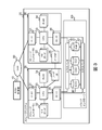
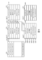
- FIG. 1 is a conceptual diagram showing an outline of a caching destination selection process according to the present invention.
- FIG. 2 is a diagram illustrating a first configuration example of the information system according to the first embodiment.
- FIG. 3 is a diagram illustrating a second configuration example of the information system according to the first embodiment.
- FIG. 4 is a configuration diagram of the FM board according to the first embodiment.
- FIG. 5 is a configuration diagram of the RAM of the storage controller according to the first embodiment.
- FIG. 6 is a configuration diagram of an access monitor table according to the first embodiment.
- FIG. 7 is a conceptual diagram of a cache management data structure according to the first embodiment.
- FIG. 8 is a diagram illustrating a partial data structure of the cache management data structure according to the first embodiment.
- FIG. 9 is a diagram illustrating a data structure of the dirty queue and the clean queue according to the first embodiment.
- FIG. 10 is a diagram illustrating a data structure of the FM free queue and the RAM free queue according to the first embodiment.
- FIG. 11 is a flowchart of read command processing according to the first embodiment.
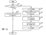
- FIG. 12 is a flowchart of the staging process according to the first embodiment.
- FIG. 13 is a flowchart of data transmission processing according to the first embodiment.
- FIG. 14 is a flowchart of the cache allocation process according to the first embodiment.
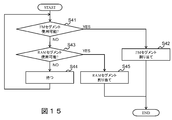
- FIG. 15 is a flowchart of FM priority segment allocation processing according to the first embodiment.
- FIG. 16 is a flowchart of RAM priority segment allocation processing according to the first embodiment.
- FIG. 17 is a flowchart of the access monitor totaling process according to the first embodiment.
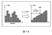
- FIG. 18 is a diagram illustrating the determination threshold value calculation method according to the first embodiment.
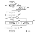
- FIG. 19 is a flowchart of write command processing according to the first embodiment.
- FIG. 20 is a flowchart of data reception processing (RAM) according to the first embodiment.
- FIG. 21 is a flowchart of data reception processing (FM) according to the first embodiment.
- FIG. 22 is a flowchart of the FM data reading process according to the first embodiment.
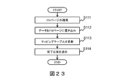
- FIG. 23 is a flowchart of the FM data writing process according to the first embodiment.
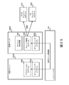
- FIG. 24 is a configuration diagram of the information system according to the second embodiment.
- FIG. 25 is a diagram illustrating an overview of data input / output processing according to the second embodiment.
- FIG. 25 is a diagram illustrating an overview of data input / output processing according to the second embodiment.
- FIG. 26 is a diagram illustrating the configuration of the information system according to the third embodiment.
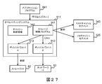
- FIG. 27 is a diagram illustrating an overview of data input / output processing according to the third embodiment.
- FIG. 28 is a configuration diagram of a job control table according to the fourth embodiment.
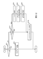
- FIG. 29 is a first flowchart of read command processing according to the fourth embodiment.
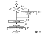
- FIG. 30 is a second flowchart of the read command process according to the fourth embodiment.
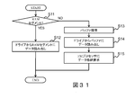
- FIG. 31 is a flowchart of the staging process according to the fourth embodiment.
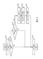
- FIG. 32 is a flowchart of data transmission processing according to the fourth embodiment.
- FIG. 33 is a flowchart of a memory type review process according to the fifth embodiment.
- FIG. 34 is a conceptual diagram showing the relationship between logical volumes and cache management data according to an embodiment of the present invention.
- FIG. 1 is a conceptual diagram showing an outline of a caching destination selection process in a storage system which is an example of an information processing apparatus of the present invention.
- the storage system is provided with a cache (disk cache) in order to improve its access performance.
- a cache has a random access memory (hereinafter referred to as “RAM”) such as a DRAM or SRAM, which is a storage medium having a higher access performance than a hard disk or the like as a final storage destination (final storage device) of data.
- RAM random access memory
- DRAM dynamic random access memory
- SRAM static random access memory
- the disadvantage of RAM is that it is expensive (high bit cost). If many caches using RAM are installed in the storage system, the average performance of the storage system can be improved, but it will be expensive. There's a problem.
- the storage system includes an FM 321 and a RAM 34 as a cache on the storage controller 30, and stores data stored in the HDD 40 or SSD 41, which is the final storage device, in either the FM 321 or the RAM 34.
- FM has a lower bit cost than RAM, it can provide a large-capacity cache storage area at a low price.
- the RAM 34 is selected as the cache destination for data that conforms to the characteristics of the RAM, and the FM 321 is selected as the cache destination for data that conforms to the characteristics of the flash memory.
- the data access characteristics for example, the access frequency of the cache target data, the access pattern, etc. are used.
- the storage controller 30 can store the data that is required to have high throughput or that the update frequency is high as flash memory.
- the RAM 34 is selected as the cache destination without being written in the cache memory using the.
- the storage system of the present invention is particularly suitable for use in a computer system in which a business application that performs data access to a large amount of data such as online transaction processing (OLTP) or ERP (Enterprise Resource Planning) is executed.
- OLTP online transaction processing
- ERP Enterprise Resource Planning
- program may be used as the subject, but the program is defined by being executed by a control device including a processor (typically a CPU (Central Processing Unit)). Since the processing is performed using the memory and the I / F (interface), the description may be made with the processor or the control device as the subject.
- the control device may be a processor, or may include a processor and a hardware circuit.
- the processing disclosed with the program as the subject may be processing performed by the host computer or the storage system. Further, part or all of the program may be realized by dedicated hardware.
- Various programs may be installed in each computer by a program distribution server or a computer-readable storage medium. As the storage medium, for example, an IC card, an SD card, a DVD, or the like may be used.
- FIG. 2 is a diagram illustrating a first configuration example of the information system according to the first embodiment.
- the information system includes a host computer 10 and a storage system 20 (an example of an information processing apparatus) connected to the host computer directly or via a network.
- the storage system 20 includes a storage controller 30 and an HDD (Hard Disk Drive) 40 and / or an SSD (Solid State Drive) 41 connected to the storage controller 30.
- the HDD 40 and / or the SSD 41 is an example of a storage device.
- the HDD 40 and / or the SSD 41 may be built in the storage controller 30.
- the storage controller 30 includes one or more front-end interface (FE I / F) 31, one or more back-end interface (BE I / F) 35, one or more FM (flash memory) boards 32, a CPU 33, and RAM (Random Access Memory) 34 is included.
- the RAM 34 is a memory (memory device) and is an example of a cache memory.
- the storage controller 30 forms one or a plurality of logical volumes (substantial logical volumes) from a plurality of storage devices (HDD 40 or SSD 41) and provides them to the host computer 10 (host computer 10 can recognize the formed logical volume).
- the host computer 10 is provided with a logical volume (virtual logical volume, and a storage area is dynamically allocated to each area in the virtual logical volume) formed by so-called thin provisioning technology. To do.
- the host computer 10 designates the provided logical volume (substantial logical volume or virtual logical volume) and the position in the logical volume (logical block number; may be abbreviated as LBA).
- a command (write command or read command) is issued to perform data read / write processing on the logical volume.
- the storage controller 30 does not provide a logical volume, for example, the storage system 20 provides the host computer 10 with each HDD 40 and each SSD 41 as a single storage device, the present invention is not limited to this. It is valid.
- a logical volume recognized by the host computer is sometimes called a logical unit (Logical Unit. LU), and unless otherwise specified in this specification, a logical volume and a logical unit.
- the term (LU) is used to mean the same concept.
- the FE I / F 31 is an interface device for communicating with the host computer 10.
- the BE I / F 35 is an interface device for communicating with the HDD 40 or the SSD 41.
- the BE I / F 35 is a SAS or Fiber Channel interface device, for example.
- the FM board 32 is a board on which an FM chip 321 (see FIG. 4) is mounted.
- the CPU 33 executes various processes.
- the RAM 34 stores programs executed by the CPU 33 and various tables.
- the RAM 34 includes a cache memory area, and the cache memory area is composed of a plurality of cache segments.
- the cache segment is a unit area managed by the CPU 33. For example, in the cache memory area in the RAM 34, area reservation, data reading, and data writing may be performed in units of cache segments.
- the final storage device is a storage device that stores data to be I / Oed by the storage controller 30 in accordance with the I / O destination specified by the I / O command. Specifically, for example, data in accordance with an I / O command (write command) is temporarily stored in a cache memory area, but then configures a logical unit (logical volume) specified by the I / O command. Storage device area (in the case where the logical volume is a virtual logical volume, the storage device area is allocated to the logical volume area).
- the final storage device means a storage device that forms this logical volume. In this embodiment, the final storage device is an HDD or an SSD, but it may be another type of storage device, for example, an external storage system having a plurality of storage devices.
- each component of the information system is illustrated one by one, but a plurality of components may be provided for redundancy, high performance, or large capacity.
- Each component may be connected via a network.
- the network may include switches and expanders.
- a configuration as shown in FIG. 3 can be considered.
- FIG. 3 is a diagram illustrating a second configuration example of the information system according to the first embodiment.
- the information system shown in FIG. 3 includes two storage controllers 30 (storage controller A and storage controller B), and these storage controllers 30 are connected via a node interface (node I / F) 36.
- the node interface 36 may be a network interface device such as Infiniband, Fiber Channel (FC), or Ethernet (registered trademark), or may be a bus interface device such as PCI Express.
- SAN Storage Area Network
- the information system has a drive enclosure 60.
- the drive enclosure 60 stores a plurality of HDDs 40 and SSDs 41.
- the plurality of HDDs 40 and SSDs 41 are connected to an expander 42 in the drive enclosure 60.
- the expander 42 is connected to the BE I / F 35 of each storage controller 30.
- the expander 42 is, for example, a SAS Expander.
- the expander 42 is, for example, an FC switch. .
- the storage system 20 includes one drive enclosure 60, but may include a plurality of drive enclosures 60.
- each drive enclosure 60 may be directly connected to each of a plurality of ports of BE I / F 35, or a plurality of drive enclosures 60 may be connected to a port of BE I / F 35 via a switch. May be.
- a plurality of drive enclosures 60 may be connected in cascade by connecting the expanders 42 of each drive enclosure 60 in cascade, and may be connected to a port of the BE I / F 35.
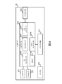
- FIG. 4 is a configuration diagram of the FM board according to the first embodiment.
- the FM board 32 includes one or more flash memory (FM) chips 321, an FM adapter 320, a bus connector 322, a buffer memory 323, and a battery 324.
- FM flash memory
- the FM board 32 which is a memory board including the flash memory chip 321 will be described as a representative example.
- a nonvolatile semiconductor memory other than the flash memory,
- a memory board including a PRAM (phase change memory), MRAM (magnetoresistance memory), or ReRAM (resistance change memory) chip may be used.
- a memory board such as the FM board 32 is a memory (memory device) and is an example of a cache memory.
- the FM chip 321 is, for example, a NAND flash memory chip.
- the plurality of FM chips 321 are used as a cache memory area, and are managed as a plurality of cache segments by the CPU 33.
- the size of one cache segment is, for example, the size of a plurality of blocks which are erase units of the FM chip 321.
- the FM chip 321 has characteristics that the access performance is lower than that of the RAM 34 and that the number of data erasures is limited.
- One FM chip 321 is composed of a plurality of blocks (physical blocks).
- One physical block is composed of a plurality of pages (physical pages).
- the bus connector 322 is a connection terminal for connecting the FM board 32 to a bus such as PCI Express on the storage controller 30.
- a bus such as PCI Express
- the bus connector 322 may be omitted.
- the buffer memory 323 is, for example, a RAM such as DRAM or SRAM, and is used as a buffer at the time of data transfer from the outside to the FM chip 321 or data transfer from the FM chip 321 to the outside.
- the buffer memory 323 may store programs executed by the FM processor 320b and data used by the FM processor 320b, the DMAC 320d, and the like.
- the battery 324 is a battery for performing power backup necessary for storing data by the buffer memory 323. Therefore, the buffer memory 323 can continuously store data by the power of the battery 324 even when the external power supply is interrupted.
- the FM adapter 320 includes an FM controller 320a, an FM processor 320b, a bus controller 320c, a DMA (Direct Memory Access) controller (DMAC) 320d, and a RAM controller 320e.
- the FM adapter 320 is an integrated circuit such as an ASIC, for example.
- the FM adapter 320 includes a circuit group of each configuration in one integrated circuit, but these circuits may be divided into a plurality of integrated circuits and mounted. Further, the function of a certain circuit (for example, DMAC 320d) may be replaced with another circuit (for example, FM processor 320b).
- FIG. 5 is a configuration diagram of the RAM of the storage controller according to the first embodiment.
- the RAM 34 is a random access memory such as DRAM or SRAM.
- the RAM 34 stores a storage control program 340 executed by the CPU 33, cache control information 341, an access monitor table 342, and a job control table 344.
- the RAM 34 stores a plurality of cache segments 343 for caching and managing data. Data stored in the HDD 40 or the SSD 41 or data read from the HDD 40 or the SSD 41 can be cached in the cache segment 343.
- the storage control program 340 is an example of a cache control program, and executes various control processes related to the cache. Details of the process will be described later.
- the cache control information 341 includes the cache directory 100 (see FIG. 7), the clean queue (see FIG. 9), the dirty queue (see FIG. 9), the FM free queue 200 (see FIG. 7), and the RAM free queue 300 (see FIG. 7). 7). A data structure related to the cache control information 341 will be described later.
- a memory module such as a DIMM in which a plurality of RAM memory chips are mounted on a board is configured, and this memory module is connected to a memory slot on the main board of the storage controller 30. It may be.
- the RAM is mounted on a board different from the main board of the storage controller 30
- maintenance replacement and RAM capacity expansion can be performed independently of the main board of the storage controller 30.
- a battery is provided so that the stored contents on the RAM 34 can be maintained even during a power failure. Also good.
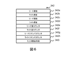
- FIG. 6 is a configuration diagram of an access monitor table according to the first embodiment.
- the access monitor table 342 stores information for counting the frequency of access to each partial area in the logical unit (logical volume) in the storage system 20 and the speed of data reading / writing, and also stores the counting result. It is a table.
- the access monitor table 342 includes, for example, a read speed 342a, a write speed 342b, a read frequency 342c, a write frequency 342d, a read amount (byte number) counter 342e, and a write amount counter 342f for each partial area in the logical unit.
- the read command counter 342g, the write command counter 342h, and the monitor start time 342i are stored.
- the size of the partial area (that is, the unit for counting access frequency and access speed in one access monitor table 342).
- the size of the partial area may be the same size as the cache segment or an integer multiple of the cache segment. ,preferable.
- the read speed 342a is a read speed for a partial area in the logical unit (for example, the unit is MB / Sec).
- the write speed 342b is a write speed (for example, the unit is MB / Sec) for a partial area in the logical unit.
- the read frequency 342c is the frequency of occurrence of reads for partial areas in the logical unit.
- the write frequency 342d is a write frequency for a partial area in the logical unit.
- the read amount counter 342e is a data amount counter of the data read in the partial area in the logical unit.
- the write amount counter 342f is a data amount counter of data written in the partial area in the logical unit.
- the read command counter 342g is a counter of the number of commands read in the partial area in the logical unit.
- the write command counter 342h is a counter of the number of commands that have been written in a partial area in the logical unit.
- the monitor start time 342i is the time at which monitoring for a partial area in the logical unit is started.
- a read amount counter 342e, a write amount counter 342f, a read command counter 342g, and a write command counter 342h are counting counters, and a read speed 342a, a write speed 342b, a read frequency 342c, and a write frequency 342d are total results. .
- About the access monitor totaling process see FIG. 17 for counting the access frequency (read frequency, write frequency) to each partial area in the logical unit in the storage system 20 and the data read / write speed (read speed, write speed). Will be described later.
- FIG. 34 is a conceptual diagram showing the relationship between logical volumes, slots, and cache segments in the embodiment of the present invention.
- the minimum access unit is a block (for example, 512 bytes), and each block of the logical volume has a logical block address (LBA. In this specification, it is called a logical address.
- LBA logical block address
- FIG. 34 represents a logical block address
- the storage system 20 performs exclusive control when accessing a storage area on a logical volume, but the concept of slot 1100 is defined as a unit of exclusive control.
- the size of the slot 1100 is 256 KB (that is, 512 blocks), but other sizes may be adopted.
- Each slot 1100 is assigned a unique identification number, which is called a slot ID.
- an element 1110 is a slot ID, and the relationship between the logical block address 1010 and the slot ID 1100 is as shown in FIG. For example, when converting a logical block address designated by an I / O command received from the host computer 10 into a slot ID, a value obtained by dividing the designated logical block address by 512 becomes the slot ID.
- the logical block address specified by the I / O command is found to be the start position of the slot (specified by the slot ID), and the remainder is 0.
- the remainder R has a block specified by the logical block address at the R-th position from the first block of the slot (specified by the slot ID). This is information indicating that it is a block (hereinafter, this information R is referred to as an in-slot relative address).
- a storage area on the RAM 34 or FM chip 321 is secured as a cache area, but a cache segment (or segment) (elements 1201, 1202, 1203, and 1204 in FIG. 34 are cache segments).
- cache segments 1201, 1202, 1203, and 1204 are collectively referred to as “cache segment 1200”), and a cache area is secured.
- the size of the cache segment 1200 is 64 KB, and four cache segments 1201, 1202, 1203, 1204 are associated with each slot.
- FIG. 34 shows a concept in which an area (cache segment 1200) on the RAM 34 or the FM chip 321 is associated with the slot 1100.
- the storage system 20 uses the slot control table 110 (details will be described when FIG. 7 is described) as slot management information. 1 exists for each slot 1100), and the information of the cache segment 1200 associated with the slot in the slot control table 110 (precisely, for managing the cache segment 1200) (Pointer to information) is stored.
- the storage system 20 manages the association between the slot 1100 and the cache segment 1200 by creating and managing the slot control table 110. Note that the size of the cache segment 1200 can be set to a size other than 64 KB, and the number of cache segments 1200 associated with one slot 1100 can be set to a value other than four.
- the outline of processing related to the management of the cache area when the host computer 10 accesses the area on the logical volume 1000 (read or write) is as follows.
- the host computer 10 provides the storage system 20 with an I / O specifying a logical unit number (a number identifying a logical unit / logical volume, generally abbreviated as LUN [Logical Unit Number]) and a logical block address 1010. Issue a command.
- the storage system 20 converts the logical block address included in the received I / O command into a pair of a slot ID 1110 and an in-slot relative address, and refers to the slot control table 110 specified by the slot ID 1110 obtained by the conversion. To do.
- the cache segment 1200 is secured for the area on the logical volume specified by the I / O command (the area specified by the logical block address). If the cache segment 1200 is not secured, processing for securing a new cache segment 1200 is performed.
- FIG. 7 is a conceptual diagram of a cache management data structure according to the first embodiment.
- the cache management data structure includes a cache directory 100, an FM free queue 200, a RAM free queue 300, a dirty queue, and a clean queue (see FIG. 9).
- cache segments (343, 325) are managed in the RAM 34 and the FM chip 321.
- Each cache segment is managed by a segment control table 120 (SGCT: Segment Control Table).
- the SGCT 120 is managed in one-to-one correspondence with each of the cache segments managed by the RAM 34 and all the FM chips 321.
- the cache directory 100 indicates the correspondence between the logical address of the data to be cached (logical block address of the logical volume that is the storage destination of data stored in the cache segment) and the physical address on the memory (RAM 34 and FM chip 321). Data structure to be managed.
- the cache directory 100 is a hash table having, for example, a logical address of cache target data (or information derived from a logical address such as a slot ID) as a key, and has a pointer for indicating the SGCT 120 as an entry.
- the SGCT 120 manages pointers to the cache segments (325, 343) corresponding to the SGCT 120.
- the cache directory 100 manages the cache segment 343 of the RAM 34 and the cache segments 325 of all the FM chips 321 together. Therefore, by referring to the cache directory 100, it is possible to easily perform cache hit determination in the RAM 34 and the FM chip 321.
- the FM free queue 200 is control information for managing a free segment of the FM chip 321, that is, a cache segment 325 in which no data is stored.
- the FM free queue 200 is configured as a bidirectional link list having, for example, an SGCT 120 corresponding to a free segment of the FM chip 321 as an entry.
- the data structure of the control information for managing the free segment is not necessarily a queue, and a stack or the like may be used.
- the RAM free queue 300 is control information for managing free segments in the RAM 34.
- the RAM free queue 300 is configured as a bidirectional link list having SGCT 120 corresponding to the free segment of the RAM 34 as an entry, for example.
- the data structure of the control information for managing the free segment is not necessarily a queue, and a stack or the like may be used.
- the SGCT 120 is connected to one of the cache directory 100, the FM free queue 200, or the RAM free queue 300 depending on the state and type of the cache segment corresponding to the SGCT 120. Specifically, the SGCT 120 corresponding to the cache segment 325 of the FM chip 321 is connected to the FM free queue 200 when the cache segment 325 is not used, and when the cache segment 325 is allocated for data storage, 100. On the other hand, the SGCT 120 corresponding to the cache segment 343 of the RAM 34 is connected to the RAM free queue 300 when the cache segment 343 is not used, and is connected to the cache directory 100 when the cache segment 343 is allocated for data storage. .
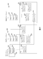
- FIG. 8 is a diagram illustrating a partial data structure of the cache management data structure according to the first embodiment.
- the cache directory 100 is a hash table using, for example, a slot ID as a key.
- the entry 100a (directory entry) of the cache directory 100 stores a directory entry pointer indicating a slot control table 110 (SLCT: Slot Control Table) corresponding to the slot ID.
- SLCT Slot Control Table
- the slot is a data unit (lock unit) for performing exclusive control.
- one slot can contain multiple cache segments. If only a part of the slot stores data, only one cache segment may be included.
- the SLCT 110 includes a directory entry pointer 110a, a forward pointer 110b, a backward pointer 110c, a slot ID 110d, a slot status 110e, and an SGCT pointer 110f.
- the directory entry pointer 110a is a directory entry pointer that points to the SLCT 110 corresponding to the next entry in the hash table.
- the forward pointer 110b is a pointer indicating the previous SLCT 110 in the clean queue or dirty queue.
- the backward pointer 110c is a pointer indicating the SLCT 110 in the subsequent order in the clean queue or the dirty queue.
- the slot ID 110d is identification information of a slot corresponding to the SLCT 110.
- the slot status 110e is information indicating the state of the slot.
- the slot state includes, for example, “locking” indicating that the slot is locked.
- the SGCT pointer 110f is a pointer that points to the SGCT 120 corresponding to the cache segment included in the slot. When no cache segment is assigned to the slot, the SGCT pointer 110f has a value (for example, NULL) indicating that the pointer (address) is invalid.
- each SGCT 120 is managed as a linked list, and the SGCT pointer 110f is a pointer pointing to the SGCT 120 corresponding to the first cache segment in the linked list.
- SGCT 120 includes an SGCT pointer 120a, a segment ID 120b, a memory type 120c, a segment address 120d, a staging bitmap 120e, and a dirty bitmap 120f.
- the SGCT pointer 120a is a pointer that points to the SGCT 120 corresponding to the next cache segment included in the same slot.
- the segment ID 120b is identification information of the cache segment, and is information indicating the number of the cache segment positioned in the slot. In the present embodiment, since up to four cache segments are allocated to one slot, any one of 0, 1, 2, and 3 is stored in the segment ID 120b of each cache segment (positioned at the head of the slot).
- the segment ID 120b of the cache segment to be assigned is 0, and the segment IDs 120b of 1, 2, and 3 are assigned in order, for example, taking the cache segments 1201 to 1204 in FIG.
- the segment ID 120b of the cache segment 1201 is 0, and the segment IDs 120b of the cache segments 1202, 1203, and 1204 are 1, 2, and 3 respectively.
- the memory type 120c is a type of cache memory in which a cache segment corresponding to the SGCT 120 is stored. As a type of cache memory, there are FM and RAM.
- the segment address 120d is a cache segment address.
- the staging bitmap 120e is a bitmap showing an area where clean data, that is, data matching the data of the drive (40, 41) is cached in the cache segment.
- each bit corresponds to each area in the cache segment, the bit corresponding to the area where valid data (the same data as the drive) is cached is set to ON (1), and the valid data is Bits corresponding to uncached areas are set to OFF (0).
- the dirty bitmap 120f is a bitmap indicating an area in the cache segment where dirty data, that is, data that does not match the drive data (data not yet reflected in the drive) is cached.
- each bit corresponds to each area in the cache segment, the bit corresponding to the area where the dirty data is cached is set to ON (1), and corresponds to the area where the dirty data is not cached. The bit is set to OFF (0).
- FIG. 9 is a diagram illustrating a data structure of the dirty queue and the clean queue according to the first embodiment.
- Dirty queues and clean queues are part of the cache data management structure.
- the dirty queue is a queue for connecting the SLCT 110 corresponding to the slot including dirty data.
- the clean queue is a queue for connecting the SLCT 110 corresponding to the slot containing only clean data.
- Dirty queues and clean queues are used for cache replacement and destage scheduling, and can take various structures depending on the cache replacement and destage scheduling schemes. In the present embodiment, an algorithm used for cache replacement and destage scheduling will be described as LRU (Least Recently Used). Note that the dirty queue and the clean queue are the same in the basic configuration of the queue except that the SLCT 110 to be connected is different, and here, the dirty queue will be described as an example.
- the dirty queue is configured as a bidirectional linked list.
- the dirty queue connects the SLCT 110 corresponding to the slot containing the recently used dirty data (the slot having the latest use time) to the forward pointer of the MRU (Most Recently Used) terminal 150, and thereafter the forward pointer 110b of the SLCT 110.
- the SLCT 110 of the next sequential slot (the slot containing the most recently used dirty data) is sequentially connected, and the LRU terminal 160 is connected to the forward pointer 110b of the last sequential SCLT 110, while the backward pointer of the LRU terminal 160 is connected.
- the SLCT 110 of the last order is connected to the backward pointer 110c of the SCLT 110 of the subsequent order, and the SLCT 110 of the previous order is sequentially connected to the MRU terminal 150.
- SLCTs 110 are arranged from the MRU terminal 150 side in the order of the last use time.
- FIG. 10 is a diagram illustrating a data structure of the FM free queue and the RAM free queue according to the first embodiment.
- the FM free queue 200 is a queue for managing the free cache segment 325 stored in the FM chip 321, and the RAM free queue 300 is a queue for managing the free cache segment 343 of the RAM 34. It is the link list which connected SGCT120 of the cache segment with the pointer.
- the FM free queue 200 and the RAM free queue 300 are the same except for the SGCT 120 to be managed.
- the free queue pointer 201 (301) of the FM free queue 200 (RAM free queue 300) points to the SGCT 120 at the head of the queue.
- the SGCT pointer 120a of the SGCT 120 points to the SGCT 120 of the next free cache segment.
- FIG. 11 is a flowchart of read command processing according to the first embodiment.
- the read command process is executed when the storage controller 30 receives a read command from the host computer 10.
- the CPU 33 of the storage controller 30 that has received the read command has a cache segment corresponding to the logical block address (hereinafter referred to as “read target address”) of the read target block on the logical volume specified by the read command. It is determined whether it has been assigned (step S1). Specifically, as described above, the logical block address is converted into a set of slot ID and in-slot relative address, and the SGCT pointer 110f in the SLCT 110 having the slot ID 110d obtained by the conversion is referred to. If the SGCT pointer 110f is an invalid (eg, NULL) value, it is determined that the cache segment is unallocated. If the SGCT pointer 110f contains a valid value, it is found that at least one cache segment is allocated.
- the SGCT pointer 110f contains a valid value, it is found that at least one cache segment is allocated.
- the SGCT pointer 110f is traced to the position in the slot specified by the relative address in the slot.
- Check whether a cache segment is allocated Specifically, by checking whether there is an SGCT 120 having the same segment ID 120b as the result (integer value) obtained by “relative address in slot ⁇ 128”, it is confirmed whether a cache segment is allocated. (By calculating the relative address in the slot ⁇ 128, an integer value of 0 to 3 can be obtained, so the cache segment to which any segment ID of 0 to 3 is assigned as the relative address in the slot.
- step S1 YES
- the CPU 33 advances the process to step S3, while if the cache segment has not been allocated (step S1: NO), the cache allocation process (FIG. 14). (Refer to step S2), and the process proceeds to step S3.
- step S2 a process of allocating the cache segment of the FM chip 321 or the cache segment of the RAM 34 is performed according to the access characteristics of the cached data.
- step S3 the CPU 33 locks the slot including the cache segment corresponding to the read target address. Specifically, the CPU 33 indicates that the slot is locked by turning on a bit indicating “locking” in the slot status 110e of the SLCT 110 of the slot including the cache segment.
- the CPU 33 determines whether or not the read target data is stored in the cache segment, that is, whether or not it is a cache hit (step S4). Specifically, the CPU 33 examines the staging bitmap 120e and the dirty bitmap 120f of the SGCT 120 corresponding to the cache segment to be read, and for all the blocks to be read, the bit or dirty of the staging bitmap 120e corresponding to the block. If any of the bits of the bitmap 120f is ON, it is determined that a cache hit has occurred. On the other hand, the CPU 33 determines that there is a cache miss when there is one block in which the corresponding bits of the dirty bitmap 120f and the staging bitmap 120e are both OFF within the range to be read.
- step S4 YES
- the CPU 33 advances the process to step S6.
- step S4: NO the staging process (see FIG. 12) is executed (step S5) The process proceeds to step S6.
- the staging process data is read from the drive (HDD 40 or SSD 41) to the cache segment (325 or 343).
- the read target data is stored in the cache segment (325 or 343).
- step S6 the CPU 33 executes a data transmission process (see FIG. 13) for transmitting the data stored in the cache segment to the host computer 10.
- the CPU 33 transmits a command completion status to the host computer 10 (step S7).
- the CPU 33 returns an error status (for example, CHECK CONDITION) if an error occurs during command processing and the read processing is not completed normally, while if the read processing is completed normally, the normal status (GOOD )return it.
- an error status for example, CHECK CONDITION
- the CPU 33 releases (unlocks) the locked slot (step S8), updates the access monitor table 342 (step S9), and ends the read command processing.
- the update of the access monitor table 342 includes, for example, adding the data amount read by the current read command to the read amount counter 342e and incrementing the read command counter 342g.
- FIG. 12 is a flowchart of the staging process according to the first embodiment.
- the staging process corresponds to the process of step S5 of the read command process of FIG.
- the CPU 33 checks the cache memory type of the cache segment corresponding to the read target address, and determines whether or not the cache segment is a cache segment (RAM segment) 343 on the RAM 34 (step S11).
- the type of the cache memory on which the cache segment is based can be specified by referring to the memory type 120c of the corresponding SGCT 120.
- step S11: YES the CPU 33 advances the process to step S12.
- step S11: NO the process proceeds to step S13. Proceed to
- step S12 the CPU 33 reads data to be read (target for staging) from the drive (HDD 40 or SSD 41), stores it in the RAM segment 343, and ends the staging process.
- step S13 since the cache segment is not the RAM segment 343, that is, the cache segment (FM segment) 325 on the FM chip 321, the data read from the drive is not directly written to the FM chip 321, but once, After the data is stored in the buffer memory 323 of the FM board 32, the data is written from the buffer memory 323 to the FM chip 321. Since the writing speed of the FM chip 321 is slow, if the data read from the drive is directly written to the FM chip 321, the operation of the BE I / F 35 of the storage controller 30 is slowed down due to the speed, and the storage system This is to prevent the throughput performance of 20 from being lowered.
- the BE I / F 35 receives data from the CPU 33 and stores data from the drive to the buffer memory 323 of the FM board 32. Therefore, the CPU 33 can execute other processes after giving an instruction to the BE I / F 35. Further, after storing data from the drive to the buffer memory 323 of the FM board 32, the BE I / F 35 is released from this process and can execute other processes.
- step S13 the CPU 33 secures an area (buffer) for storing data read from the drive in the buffer memory 323. That is, the CPU 33 allocates a sufficient area in the buffer memory 323 to store the data to be staged.
- the CPU 33 reads out the data to be staged from the drive and stores it in the buffer (step S14).
- the BE I / F 35 receives data from the CPU 33 and stores data from the drive to the buffer of the buffer memory 323 of the FM board 32.
- the CPU 33 requests the FM processor 320b to store the data on the buffer of the buffer memory 323 in the FM chip 321 (step S15).
- the FM processor 320b executes FM data write processing (see FIG. 23).
- the FM processor 320b finishes the FM data writing process, it returns a completion response to the request to the CPU 33.
- the CPU 33 receives a completion response to the request from the FM processor 320b (step S16), releases the buffer of the buffer memory 323 (step S17), and ends the staging process.
- FIG. 13 is a flowchart of data transmission processing according to the first embodiment.
- the data transmission process corresponds to the process of step S6 of the read command process shown in FIG.
- the data transmission process when data is transmitted from the FM segment 325, the data is temporarily stored in the buffer memory 323, and the data is transferred from the buffer memory 323 to the host computer 10. This is because the reading speed of the FM chip 321 is slow, and if it is directly transferred from the FM chip 321, the operation of the FE I / F 31 of the storage controller 30 is slowed down due to the speed, and the throughput performance of the storage system 20 is lowered. This is to prevent that.
- the CPU 33 checks the type of the cache memory that is the basis of the cache segment corresponding to the read target address, and determines whether or not the cache segment is the RAM segment 343 (step S21).
- the type of the cache memory on which the cache segment is based can be specified by referring to the memory type 120c of the corresponding SGCT 120.
- step S21: YES if the cache segment is the RAM segment 343 (step S21: YES), the CPU 33 advances the process to step S22. On the other hand, if the cache segment is not the RAM segment 343 (step S21: NO), the process proceeds to step S23. Proceed to
- step S22 the CPU 33 transfers the read target (transmission target) data from the RAM segment 343 to the host computer 10 and ends the data transmission process.
- step S23 the CPU 33 secures an area (buffer) for storing the transmission target data read from the FM chip 321 in the buffer memory 323. That is, the CPU 33 allocates a sufficient area in the buffer memory 323 to store data to be transmitted.
- the CPU 33 requests the FM processor 320b to read data on the FM chip 321 to the buffer memory 323 (step S24).
- the FM processor 320b executes FM data read processing (see FIG. 22).
- the transmission target data is stored in the buffer memory 323.
- the FM processor 320b finishes the FM data reading process, it returns a completion response to the request to the CPU 33.
- the CPU 33 receives a completion response to the request from the FM processor 320b (step S25), and transmits data to be transmitted from the buffer memory 323 to the host computer 10 (step S26).
- the FE I / F 31 transmits the data to be transmitted from the buffer of the buffer memory 323 to the host computer 10 in response to an instruction from the CPU 33 (for example, an address on the buffer memory 323 of the data to be read). is doing.
- the CPU 33 releases the buffer in the buffer memory 323 (step S27), and ends the data transmission process.
- FIG. 14 is a flowchart of the cache allocation process according to the first embodiment.
- the cache allocation process corresponds to the process of step S2 of the read command process shown in FIG. 11 and the process of step S72 of the write command process shown in FIG.
- the cache segment of the FM chip 321 or the cache segment of the RAM 34 is allocated to the data cached by the CPU 33 according to the access characteristics for the data.
- the memory type of the cache segment to be allocated that is, the criterion for selecting the FM chip 321 or the RAM 34
- the FM chip 321 has characteristics that (1) access performance is lower than that of the RAM 34 and (2) there is an upper limit on the number of rewrites
- the CPU 33 has data characteristics.
- the cache segment using the RAM 34 is selected, and the data is compatible with the characteristics of the flash memory. (Not so high performance is required, and the update frequency of the cache segment is not high) performs control to select a cache segment using the FM chip 321.
- the memory type of the cache segment to be allocated is selected based on the following criteria.
- A In the case of data with a high access frequency (read frequency / write frequency) or data that requires high throughput, the CPU 33 preferentially selects the RAM 34.
- the update frequency of the FM chip 321 increases. If the update frequency is high, rewriting occurs frequently and the life of the FM chip 321 is shortened, so it is better to preferentially select the RAM 34. Thereby, shortening of the lifetime of the FM chip 321 can be appropriately suppressed. Further, as data requiring high throughput, for example, a large amount of data read for use in an in-memory database is applicable.
- data for this purpose is often data having a long transfer length or data for sequential access. Therefore, the RAM 34 is preferentially selected for data determined to have a long transfer length. Thereby, high throughput can be realized.
- the CPU 33 preferentially selects the RAM 34. For example, data stored in the SSD 41 may be used as data for which the performance effect due to the cache hit is not obtained. According to this, it is possible to appropriately obtain the effect of the cache hit.
- C If data with a small access unit is a cache target, the CPU 33 preferentially selects the RAM 34.
- the size of the read / write unit (page) in the FM chip 321 is larger than the minimum access unit in the RAM 34 (for example, 8 KB), and the efficiency of referring / updating data in a small unit is poor.
- metadata such as control information is usually about 16 B in size, and is smaller than the size of the read / write unit of the FM chip 321, so it should be cached in the RAM 34.
- D When data that is immediately discarded from the cache is a cache target, the CPU 33 preferentially selects the RAM 34. The reason is that the FM chip 321 is erased immediately when it is discarded, and if it is immediately discarded, the capacity consumption is temporary even if it is placed in the RAM 34, and the influence is small.
- What kind of data is discarded preferentially is set as a policy of the storage system. For example, data stored in a temporary cache segment allocated for data copy is discarded from the cache when the copy process is completed. As another example, there is data to be sequentially read and data to be sequentially written. For data to be sequentially read, it is basically not read from the beginning in order, and the data of the same part is not read immediately after reading. For example, when the data to be sequentially written is stored in RAID, the data is destaged when necessary parity is prepared, and then discarded from the cache. (E) When data that satisfies conditions other than the above (a) to (d) is a cache target, the CPU 33 preferentially selects the FM chip 321.
- the CPU 33 determines whether the data to be accessed (read target or write target) is data to be accessed at high speed (step S31). Specifically, for example, the CPU 33 compares the access speed threshold obtained in advance with the read speed 342a and write speed 342b of the area where the access target data recorded in the access monitor table 342 is stored. It is determined whether the data to be accessed is data that is accessed at high speed. The counting method of the read speed 342a and the write speed 342b will be described later. However, when the data access frequency is high or when the data having a long transfer length is accessed, the read speed 342a and the write speed 342b that are tabulated in this embodiment are high.
- the access frequency (the read frequency 342c or the write frequency 342d of the area in which the access target data is stored, which is recorded in the access monitor table 342) may be compared with a threshold value for determination. If the determination result in step S31 is true (step S31: YES), the CPU 33 advances the process to step S37, while if false (step S31: NO), the process advances to step S32.
- step S32 the CPU 33 determines whether or not the access pattern for the access target data is sequential access. This determination can be realized by the CPU 33 determining whether or not the read command to be processed is part of a series of commands that sequentially read consecutive addresses. Specifically, for example, the CPU 33 performs sequential access by determining whether an address obtained by adding the transfer length of the command to the target address of the previous read command is the target address of the current read command. It is determined whether or not. As a result, when it is determined that the access is sequential (step S32: YES), the CPU 33 advances the process to step S37. On the other hand, when it is determined that the access is false (step S32: NO), the CPU 33 performs the process. Proceed to step S33.
- step S33 the CPU 33 determines whether or not the access target data is data that is finally stored in the SSD 41, that is, whether or not the final storage device of the access target data is the SSD 41.
- whether or not the final storage device of the access target data is the SSD 41 is determined based on, for example, the logical volume specified by the read command based on the information indicating the correspondence relationship between the logical volume and the device stored in advance. This can be realized by specifying the device type corresponding to the volume. If the logical volume conforms to thin provisioning, it is determined whether or not the final storage device of the access target data is the SSD 41 by specifying the device type of the device that provides the real page allocated to the logical volume. can do. If the result is true (step S33: YES), the CPU 33 advances the process to step S37, and if false, advances the process to step S34.
- step S34 the CPU 33 determines whether the data to be accessed is metadata.
- the metadata here includes control information that is saved / stored in the drive (40, 41) from the RAM 34 of the storage controller 30 or saved / stored.
- whether or not the access target data is metadata can be determined, for example, based on whether or not the access destination is a predetermined area in which control information in the logical volume is stored. Note that the address of the area where the control information in the logical volume is stored can be obtained from the host computer 10 or the like that uses the logical volume. If the result is true (step 34: YES), the CPU 33 advances the process to step S37, and if false, advances the process to step S35.
- step S35 the CPU 33 determines whether or not the cache segment corresponding to the access target data is a temporary cache segment (temporary segment).
- the temporary segment is one of the following. (1) A segment allocated for storing old data or old parity when old data or old parity has a cache miss in parity generation. (2) A segment temporarily allocated for a process of copying data of a drive (for example, a final storage device). (3) A segment temporarily allocated for processing of transmitting / receiving data to / from another storage apparatus (for example, for remote copy processing).
- the CPU 33 receives information indicating whether the throughput is high throughput or information indicating the priority of the I / O from the host computer 10 when allocating the cache segment to the data, and determines whether the data is the high throughput.
- the information indicating or the information indicating the priority of I / O may be stored in association with the cache segment, and based on the information, it may be determined whether or not the cache segment is a temporary segment. .
- step 35 If the result is true (step 35: YES), the CPU 33 advances the process to step S37, and if false, advances the process to step S36.
- step S36 the CPU 33 executes FM priority segment allocation processing (see FIG. 15) for preferentially allocating the cache segment 325 of the FM chip 321 and ends the cache allocation processing.
- step S37 the CPU 33 executes a RAM priority segment allocation process (see FIG. 16) for preferentially allocating the cache segment 343 of the RAM 34, and ends the cache allocation process.
- one of the cache segments of the FM chip 321 or the RAM 34 is allocated to the data to be accessed.
- FIG. 15 is a flowchart of FM priority segment allocation processing according to the first embodiment.
- FM priority segment allocation processing is processing corresponding to step S36 of the cache allocation processing shown in FIG.
- step S41 the CPU 33 determines whether there is an available FM segment 325 (step S41).
- An available FM segment 325 is a cache segment 325 that is free or clean and not locked. Note that whether there is an available FM segment 325 can be determined by referring to the cache management data structure.
- step S41: YES the CPU 33 advances the process to step 42, whereas when false (step S41: NO), the process advances to step S43.
- step S42 the CPU 33 performs FM segment allocation processing.
- the CPU 33 separates the cache segment from the clean queue and the cache directory 100 to make a free segment, and then performs an FM segment allocation process.
- the CPU 33 sets a segment ID 120b and a memory type 120c (FM) corresponding to the cache segment secured in the SGCT 120. Then, the CPU 33 sets a pointer to the SGCT 120 of the cache segment in the SGCT pointer 110f of the SLCT 110 corresponding to the slot including the cache segment. If the corresponding SLCT 110 is not connected to the cache directory 100, the CPU 33 first sets the contents of the SLCT 110, connects the SLCT 110 to the cache directory 100, and then connects the SGCT 120 to the SLCT 110.
- FM memory type 120c
- the CPU 33 connects the SGCT 120 of the reserved cache segment to the terminal SGCT 120 connected to the SLCT 110. . Note that after the FM segment allocation process ends, the FM priority segment allocation process ends.
- step S43 the CPU 33 determines whether there is a usable RAM segment 343. If the determination result is true (step S43: YES), the CPU 33 advances the process to step S45. If the determination result is false (step S43: NO), the CPU 33 waits until one of the cache segments becomes usable. (Step S44), the process proceeds to Step S41.
- step S45 the CPU 33 performs a RAM segment allocation process.
- the RAM segment 343 is allocated to the one allocated to the FM segment 325 in the FM segment allocation process in step S42.
- the FM priority segment allocation process ends.
- the FM segment 325 is preferentially allocated.
- FIG. 16 is a flowchart of RAM priority segment allocation processing according to the first embodiment.
- the RAM priority segment allocation process is a process corresponding to step S37 of the cache allocation process shown in FIG.
- the RAM priority segment allocation process is a process in which the FM segment and the RAM segment in the FM priority segment allocation process shown in FIG. 15 are interchanged, and will be briefly described here.
- step S51 determines whether there is a usable RAM segment 343 (step S51). If this determination result is true (step S51: YES), the CPU 33 advances the process to step S52, whereas if false (step S51: NO), the process advances to step S53.
- step S52 the CPU 33 performs a RAM segment allocation process.
- This RAM segment allocation process is the same process as step S45 of FIG. After the RAM segment allocation process ends, the RAM priority segment allocation process ends.
- step S53 the CPU 33 determines whether there is an available FM segment 325 or not. If the determination result is true (step S53: YES), the CPU 33 advances the process to step S55. If the determination result is false (step S53: NO), the CPU 33 waits until one of the cache segments becomes usable. (Step S54), the process proceeds to Step S51.
- step S55 the CPU 33 performs FM segment allocation processing.
- This FM segment allocation process is the same process as step S42 of FIG. After the FM segment allocation process ends, the RAM priority segment allocation process ends.
- the RAM segment 343 is preferentially allocated.
- FIG. 17 is a flowchart of access monitor tabulation processing according to the first embodiment.
- the access monitor tabulation process is a process that is executed, for example, at a fixed time period, and updates the access monitor table 342 by tabulating the read / write amount and the read / write frequency during that period.
- the CPU 33 updates the read speed 342a of the access monitor table 342 (step S61). That is, the CPU 33 sets the value obtained by dividing the value of the read amount counter 342e by the time from the monitor start time 342i to the present time (hereinafter referred to as monitor time) as the read speed in the read speed 342a of the access monitor table 342. To do.
- the CPU 33 updates the write speed 342b of the access monitor table 342 (step S62). That is, the CPU 33 sets the value obtained by dividing the value of the write amount counter 342f by the monitor time as the write speed in the write speed 342b of the access monitor table 342.
- the CPU 33 updates the read frequency 342c of the access monitor table 342 (step S63). That is, the CPU 33 sets a value obtained by dividing the value of the read command counter 342g by the monitor time as a read frequency in the read frequency 342c of the access monitor table 342.
- the CPU 33 updates the write frequency 342d of the access monitor table 342 (step S64). That is, the CPU 33 sets a value obtained by dividing the value of the write command counter 342h by the monitor time as the write frequency in the write frequency 342d of the access monitor table 342.
- the CPU 33 sets the current time to the monitor start time 342i of the access monitor table 342 (step S65), and sets the values of the read amount counter 342e, the write amount counter 342f, the read command counter 342g, and the write command counter 342h to 0. Reset (step S66) and end the access monitor tabulation process.
- This access monitor tabulation process can appropriately grasp the write speed, read speed, write frequency, and read frequency for each partial area in the logical unit.
- the read speed and the write speed are calculated by dividing the read amount / write amount by the monitor time.
- the access monitor table 342 includes a read command, The accumulation of the write command processing time (the time required from receiving the command to returning the response to the host computer 10) is stored, and the read amount and write amount are respectively processed for the read command and the write command. You may make it divide by accumulation of. Assuming that a command (read or write command) is issued multiple times for a partial area in the logical unit, the transfer length is calculated by calculating the access speed by dividing the read amount / write amount by the monitor time. Even when accessing long data, if the time interval between issued commands is long, the calculated access speed is low.
- the read speed and write speed are values obtained by dividing the read amount and write amount by the accumulated read command and write command processing time, respectively, the time interval of commands issued to a certain partial area in the logical unit is long. Regardless of the short, when accessing data with a long transfer length, the calculated read speed and write speed increase, so the time interval of commands issued to a certain partial area in the logical unit is If you want to preferentially cache in RAM when accessing data with long transfer length, regardless of whether it is long or short, divide the read amount and write amount by the accumulated processing time of the read command and write command, respectively. These values should be used as the read speed and write speed.
- the access monitor table 342 is provided for each partial area in the logical unit, and the access frequency and access speed are totaled for each partial area. As described above, various sizes can be selected as the size of the partial area (that is, the unit for counting access frequency and access speed in one access monitor table 342). However, in the storage system of the present invention, the access monitor In order to determine the memory type to be allocated as the cache segment based on the information in the table 342, when the memory type to be allocated as the cache segment is determined, the processing in FIG. 14 and the like is determined in units of cache segments. As a result, the memory type assigned to each partial area unit is determined.
- the size of the partial area when it is desired to select the type of cache memory to be allocated for each area as small as possible, it is preferable to reduce the size of the partial area. For example, if the size of the partial area is the same size as the cache segment, memory allocation according to the access characteristics for each cache segment becomes possible. However, if the size of the partial area is small, the amount of the access monitor table 342 to be maintained increases, so it may be an integer multiple of the cache segment size (for example, the slot size) or an integer multiple of the slot size.
- the access monitor table 342 and the access monitor aggregation process in the first embodiment are provided exclusively for performing the cache allocation process, but as another embodiment, other than the cache allocation process in the storage system 20
- the information aggregated by the means may be used.
- a storage device that provides a logical volume in accordance with so-called thin provisioning includes each partial area (page and page) of a logical volume.
- the access frequency information tabulated for each page is stored. It may be used to determine cache allocation.
- FIG. 18 is a diagram illustrating the determination threshold value calculation method according to the first embodiment.
- the threshold used as a reference when determining whether or not the target data is accessed at high speed is that the life of the FM chip 321 used in the FM board 32 is excessively short. It is desirable to set a value so that the update / erase frequency for the FM chip 321 does not become too high. Therefore, the threshold value is determined in consideration of the number of rewrites and capacity of the FM chip 321 used, the performance of the storage system 20 (for example, the write frequency from the host computer 10), and the like. This threshold value may be a predetermined fixed value, but may be dynamically determined using the value of the access monitor table 342 as described below. In this way, a threshold value that is more suitable for the situation can be set.
- the CPU 33 sorts the areas (partial areas) at the write speed as shown in the left graph of FIG. 18 in the descending order of the write speed, as shown in the right graph of FIG.
- each area is a partial area managed by the access monitor table 342.
- the write speeds of the respective areas are added in order, and when the total exceeds the allowable total write speed obtained by Expression (1), it is determined whether or not the target data is accessed at high speed based on the write speed of the areas.
- the threshold value is used as a reference. That is, an area having a write speed lower than the write speed of the area is an area suitable for caching by the FM chip 321 (FM appropriate area), and this area is cached in the FM chip 321 and other areas are cached. Is not cached in the FM chip 321.
- Allowable total write speed Remaining write capacity / (Remaining usage period x Margin)-Other FM update speed (1)
- the remaining writable amount is the number of remaining rewritable times and capacity of the FM chip 321, and WA (Write Amplification: an index indicating how many times the write amount to the flash memory is amplified by reclamation or wear leveling) It depends on.
- the other FM update speed is a speed at which the FM chip 321 is updated by processing other than the write from the host computer 10, for example, cache replacement or destage.
- the remaining use period corresponds to a period up to a date assumed to replace the FM chip 321.
- the allocation of the cache to the FM board 32 on which the FM chip 321 is mounted can be stopped and replaced with a new FM board 32.
- the CPU 33 sets the allowable total write speed to zero. By doing so, the FM segment is not assigned.
- the CPU 33 displays a message prompting the replacement of the FM board 32 on the management terminal or sends an e-mail to the administrator to notify the administrator that the FM board 32 needs to be replaced. Inform.
- the CPU 33 When replacing the FM board 32, the CPU 33 first writes out the dirty data remaining on the old FM board 32 to the drive, and then displays a notification that it can be removed, for example, on the management terminal. After the administrator removes the old FM board 32 from the storage controller 30 and inserts the new FM board 32 into the storage controller 30, the CPU 33 initializes the new FM board 32 and initializes the remaining writable amount. Similarly, the allowable total write speed is calculated. As a result, FM segment allocation is performed using the new FM board 32 thereafter.
- FIG. 19 is a flowchart of the write command process according to the first embodiment.
- the write command process is executed when the storage controller 30 receives a write command from the host computer 10.
- the CPU 33 of the storage controller 30 determines whether or not a cache segment corresponding to the logical block address (write target address) of the write target logical volume designated by the write command has been allocated. Determination is made (step S71). Since this process is the same as the read process (S1 in FIG. 11), detailed description thereof is omitted. As a result, if the cache segment has been allocated (step S71: YES), the process proceeds to step S73. On the other hand, if the cache segment has not been allocated (step S71: NO), the cache allocation process (see FIG. 14) is performed. Execute (step S72), and proceed to step S73. In the cache allocation process, a cache segment is allocated from the RAM 34 or the FM chip 321 to the write target address. Note that two cache segments may be allocated in order to ensure reliability by duplicating the written data.
- step S73 the CPU 33 locks the slot including the cache segment corresponding to the write target address. Specifically, the CPU 33 indicates that the slot is locked by turning on a bit indicating “locking” in the slot status 110e of the SLCT 110 of the slot including the cache segment.
- the CPU 33 notifies the host computer 10 that, for example, XFER_RDY is transmitted, that data is ready to be received (step S74).
- the CPU 33 determines whether or not the allocated cache segment is the RAM segment 343 (step S75). As a result, if the allocated cache segment is the RAM segment 343 (step S75: YES), the CPU 33 performs a data reception process (RAM) (see FIG. 20) for storing the data received from the host computer 10 in the RAM segment 343. Execute (step S76), and the process proceeds to step S78. On the other hand, if the allocated cache segment is the FM segment 325 (step S75: NO), the CPU 33 executes data reception processing (FM) (see FIG. 21) for storing the data received from the host computer 10 in the FM segment 325. (Step S77), and the process proceeds to Step S78.
- RAM data reception process
- FM data reception processing
- step S78 the CPU 33 updates the access monitor table 342. That is, the CPU 33 adds the data amount received by the current write command to the write amount counter 342f of the access monitor table 342, and increments the write command counter 342h. Thereafter, the CPU 33 ends the write command process.
- FIG. 20 is a flowchart of data reception processing (RAM) according to the first embodiment.
- the data reception process (RAM) corresponds to the process of step S76 of the write command process shown in FIG.
- the CPU 33 writes the data received from the host computer 10 to the RAM segment 343 (step S81).
- the CPU 33 sets that the written data is dirty data (step S82). That is, the CPU 33 sets ON the bit corresponding to the block in which the received data is written in the dirty bitmap 120f of the SGCT 120.
- the CPU 33 transmits a command completion status to the host computer 10, releases (unlocks) the slot including the RAM segment 343 (step S84), and ends the data reception process (RAM).
- FIG. 21 is a flowchart of data reception processing (FM) according to the first embodiment.
- the data reception process (FM) corresponds to the process of step S77 of the write command process shown in FIG.
- the CPU 33 writes the data received from the host computer 10 to the buffer memory 323 of the FM board 32 (step S91).
- the CPU 33 tests whether the written data can be read from the buffer memory 323 (step S92). At this time, the CPU 33 may confirm that the data is normal by checking a guarantee code such as CRC (Cyclic Redundancy Check) added to the data.
- CRC Cyclic Redundancy Check
- the CPU 33 sets the written data as dirty data (step S93). That is, the CPU 33 turns on the bit corresponding to the block in which the received data is written in the dirty bitmap 120f of the SGCT 120.
- the CPU 33 transmits a command completion status to the host computer 10 and releases a slot including the FM segment 325 (step S95).
- the CPU 33 requests the FM processor 302b to store the data on the buffer memory 323 in the cache segment 325 of the FM chip 321 (step S96), and ends the data reception process (FM).
- FIG. 22 is a flowchart of the FM data reading process according to the first embodiment.
- the FM data reading process is executed when the FM processor 320b receives a request to read data on the FM chip 321 into the buffer in step S24 of the data transmission process shown in FIG.
- the FM processor 320b converts the logical address designated by the CPU 33 of the storage controller 30 into a physical address representing a data storage position on the FM chip 321 (step S101). Note that the conversion from a logical address to a physical address can be performed based on a mapping table indicating the correspondence between the logical address and the physical address stored in the buffer memory 323.
- the FM processor 320b reads the target data from the area corresponding to the physical address of the FM chip 321 and stores it in the buffer memory 323 (step S102).
- the FM processor 320b transmits a completion response to the CPU 33 of the storage controller 30 (step S103), and ends the FM data reading process.
- FIG. 23 is a flowchart of the FM data writing process according to the first embodiment.
- the FM data write process is executed when the FM processor 320b receives a request to store the data on the buffer memory 323 in the cache segment 325 of the FM chip 321 in step S96 of the data reception process (FM) shown in FIG. Is done.
- the FM processor 320b secures a page (also referred to as an FM page) of the FM chip 321 that is a data storage destination (step S111).
- the FM processor 320b selects an already erased FM page as a data storage destination. If there is no erased FM page, the FM processor 320b selects an empty block of the FM chip 321 (also referred to as an empty FM block), that is, a block of the FM chip 321 that does not store valid data (also referred to as an FM block). Erasing and selecting a necessary amount of FM pages from the top of the FM block as a data storage destination.
- the FM processor 320b writes the data on the buffer memory 323 to the secured FM page (step S112).
- the FM processor 320b updates the mapping table representing the correspondence relationship between the logical address and the physical address so that the logical address to be processed this time corresponds to the physical address of the FM page in which data is newly stored.
- the fact that the FM page storing the old data is invalid is stored (step S1 13).
- the FM processor 320b manages the FM block as a free FM block.
- the data of the empty FM block may be erased, or the data of the empty FM block may be erased later as background processing.
- the FM processor 320b transmits a completion response to the CPU 33 of the storage controller 30 (step S114), and ends the FM data writing process.
- FIG. 24 is a configuration diagram of an information system according to the second embodiment.
- symbol is attached
- FIG. 24 is a configuration diagram of an information system according to the second embodiment.
- symbol is attached
- the main difference between the information system according to the second embodiment and the information system according to the first embodiment is that the FM board 32 is mounted on the host computer 80.
- This host computer 80 is an example of an information processing apparatus.
- the information system according to the second embodiment includes a host computer 80 and an HDD 40, SSD 41, or storage system 20 connected to the host computer 80 directly or via a network.
- the host computer 80 includes a CPU 81, a RAM 84, an FM board 32, a storage interface 82, and a network interface 83.
- the storage interface 82 is an interface for connecting the HDD 40 or the SSD 41.
- the network interface 83 is an interface for connecting to the storage system 20 via a network.
- the FM board 32 has the same configuration as the FM board according to the first embodiment shown in FIG.
- the RAM 84 stores an application program 841 executed by the CPU 81, an operating system 842 (operating system A, operating system B), a hypervisor program 843, a storage control program 340, and cache control information 341.
- the RAM 84 stores a cache segment 343 for caching data.
- the hypervisor program 843 is a program for managing a virtual machine (VM) constructed by the host computer 80. Note that the function of the hypervisor program 843 may be implemented as hardware.
- FIG. 25 is a diagram illustrating an outline of data input / output processing according to the second embodiment.
- the hypervisor HV constructed by the CPU 81 executing the hypervisor program 843 is located in the lowest hierarchy.
- the hypervisor HV is a kind of virtualization mechanism.
- the virtualization mechanism may be a computer having a processor that executes a program.
- One or more virtual machines (in FIG. 25, a virtual machine A (VMA) and a virtual machine B (VMB) are realized by the hypervisor HV.
- VMA virtual machine A
- VMB virtual machine B
- the storage control program 340 uses the cache segment 343 of the RAM 34 and the cache segment 325 of the FM chip 321.
- the cache is controlled in the same way as in Example 1.
- the storage control program 340 also controls data input / output with respect to the HDD 40, SSD 41, or storage system 20 connected to the host computer 80.
- the application program 841 of the virtual machine A and the storage control program 340 of the virtual machine B communicate with each other by inter-virtual machine communication.
- This inter-virtual machine communication is virtualized by the hypervisor HV or each operating system 842, and for the application program 841 and the storage control program 340, for example, the same virtual communication as that via a storage interface such as SCSI is used. This may be done using an interface.
- the host computer 80 can appropriately cache data using the RAM cache segment 343 and the FM cache segment 325.
- FIG. 26 is a diagram illustrating a configuration of the information system according to the third embodiment.
- the information system according to the third embodiment is different from the information system according to the second embodiment in the contents managed by the RAM in the host computer.
- the host computer 90 includes a RAM 91.
- the host computer 90 is an example of an information processing apparatus.
- the RAM 91 stores an operating system 911.
- the operating system 911 includes a storage control program 340 and cache control information 341 as drivers.
- FIG. 27 is a diagram illustrating an outline of data input / output processing according to the third embodiment.
- the storage control program 341 included in the operating system 911 processes this input / output request.
- caching is performed on the RAM cache segment 343 and the FM cache segment 325.
- the storage control program 341 passes an input / output request for storage to various device drivers (912, 913) in order to input / output to / from the storage.
- the device driver A 912 controls the storage interface 82 based on the input / output request.
- the device driver B 913 controls the network interface 83 based on the input / output request.
- the operating system 911 of the host computer 90 can appropriately cache data by using the RAM cache segment 343 and the FM cache segment 325.
- the difference between the information system according to the fourth embodiment and the information system according to the first embodiment is a read command processing procedure.
- the data staged from the drive is first transmitted from the buffer memory 323 to the host computer 10 before being written from the buffer memory 323 to the FM chip 321, and then written to the FM chip 321.
- the time required for completion of the read command (response time) can be shortened.
- FIG. 28 is a configuration diagram of a job control table according to the fourth embodiment.
- the job control table 344 stores a job type 344a, a logical unit number 344b, a logical block address 344c, a transfer length 344d, and a buffer address 344e.
- the job type 344a represents the type of processing performed by the job.
- the job type 344a is an ID indicating a job such as “1” for read command processing and “2” for write command processing, for example.
- the logical unit number 344b, the logical block address 344c, and the transfer length 344d are the logical unit number, logical block address (LBA), and transfer specified for the access target specified in the read / write command received from the host computer 10, respectively. Represents length.
- the buffer address 344e represents the address of the buffer secured by this job.
- the buffer address 344e is a value (for example, NULL) indicating that the address is invalid when the buffer is not secured.
- FIG. 29 is a first flowchart of a read command process according to the fourth embodiment
- FIG. 30 is a second flowchart of a read command process according to the fourth embodiment.
- the symbol A in the flowchart of FIG. 29 indicates that it is connected to the symbol A in the flowchart of FIG.
- the read command process is executed when the storage controller 30 receives a read command from the host computer 10.
- the CPU 33 of the storage controller 30 determines whether or not a cache segment corresponding to the read target address specified by the read command has been allocated (step S1). As a result, if the cache segment has been allocated (step S1: YES), the CPU 33 advances the process to step S3, while if the cache segment has not been allocated (step S1: NO), the cache allocation process (FIG. 14). (Refer to step S2), and the process proceeds to step S3.
- the cache allocation process is as described in the first embodiment.
- step S3 the CPU 33 locks the slot including the cache segment corresponding to the read target address. Specifically, the CPU 33 indicates that the slot is locked by turning on a bit indicating “locking” in the slot status 110e of the SLCT 110 of the slot including the cache segment.
- the CPU 33 determines whether or not the read target data is stored in the cache segment, that is, whether or not it is a cache hit (step S4). Specifically, the CPU 33 examines the staging bitmap 120e and the dirty bitmap 120f of the SGCT 120 corresponding to the cache segment to be read, and for all the blocks to be read, the bit or dirty of the staging bitmap 120e corresponding to the block. If any of the bits of the bitmap 120f is ON, it is determined that a cache hit has occurred. On the other hand, the CPU 33 determines that there is a cache miss when there is one block in which the corresponding bits of the dirty bitmap 120f and the staging bitmap 120e are both OFF within the range to be read.
- step S4 YES
- the CPU 33 advances the process to step S122
- step S4: NO the staging process (see FIG. 31) is executed (step 31).
- step S121) the process proceeds to step S122.
- the staging process data is read from the drive (HDD 40 or SSD 41) to the cache segment (325 or 343).
- the read target data is stored in the cache segment (325 or 343).
- step S122 the CPU 33 executes a data transmission process (see FIG. 32) for transmitting the data stored in the cache segment to the host computer 10.
- the CPU 33 transmits a command completion status to the host computer 10 (step S7).
- the CPU 33 returns an error status (for example, CHECK CONDITION) if an error occurs during command processing and the read processing is not completed normally, while if the read processing is completed normally, the normal status (GOOD )return it.
- an error status for example, CHECK CONDITION
- step S123 the CPU 33 determines whether or not writing to the FM chip 321 is being performed. “Writing to the FM chip 321” means a state in which a data write request from the buffer memory 323 to the FM chip 321 is transmitted to the FM processor 320b and a completion notification is not yet received from the FM processor 320b. To do. If the result is true (step S123: YES), the CPU 33 waits for a completion notification from the FM processor 320b (step S124), and advances the process to step S125. On the other hand, if it is false (step S123: NO), the CPU 33 advances the process to step S125.
- step S125 the CPU 33 releases the buffer.
- the CPU 33 releases (unlocks) the locked slot (step S8), updates the access monitor table 342 (step S9), and ends the read command processing.
- the update of the access monitor table 342 includes, for example, adding the data amount read by the current read command to the read amount counter 342e and incrementing the read command counter 342g.
- FIG. 31 is a flowchart of staging processing according to the fourth embodiment.
- the staging process corresponds to the process of step S121 of the read command process of FIG.
- the CPU 33 checks the type of the cache memory that is the basis of the cache segment assigned to the read target address, and determines whether or not the cache segment is a cache segment (RAM segment) 343 on the RAM 34 (step). S11).
- the type of the cache memory on which the cache segment is based can be specified by referring to the memory type 120c of the corresponding SGCT 120.
- step S11: YES the CPU 33 advances the process to step S12.
- step S11: NO the process proceeds to step S13. Proceed to
- step S12 the CPU 33 reads data to be read (target for staging) from the drive (HDD 40 or SSD 41), stores it in the RAM segment 343, and ends the staging process.
- step S13 since the cache segment is not the RAM segment 343, that is, the cache segment (FM segment) 325 on the FM chip 321, the data read from the drive is not directly written to the FM chip 321, but once, After the data is stored in the buffer memory 323 of the FM board 32, the data is written from the buffer memory 323 to the FM chip 321.
- step S13 the CPU 33 secures an area (buffer) for storing data read from the drive in the buffer memory 323. That is, the CPU 33 allocates a sufficient area in the buffer memory 323 to store the data to be staged.
- the CPU 33 reads out the data to be staged from the drive and stores it in the buffer (step S14).
- the BE I / F 35 receives data from the CPU 33 and stores data from the drive to the buffer of the buffer memory 323 of the FM board 32.
- the CPU 33 requests the FM processor 320b to store the data on the buffer of the buffer memory 323 in the FM chip 321 (step S15).
- the FM processor 320b executes a data transmission process (see FIG. 32).
- FIG. 32 is a flowchart of data transmission processing according to the fourth embodiment.
- the data transmission process corresponds to the process of step S122 of the read command process shown in FIG.
- the CPU 33 checks the type of the cache memory that is the basis of the cache segment assigned to the read target address, and determines whether or not the cache segment is the RAM segment 343 (step S21).
- the type of the cache memory on which the cache segment is based can be specified by referring to the memory type 120c of the corresponding SGCT 120.
- step S21: YES if the cache segment is the RAM segment 343 (step S21: YES), the CPU 33 advances the process to step S22, while if the cache segment is not the RAM segment 343 (step S21: NO), the process proceeds to step S131. Proceed to
- step S22 the CPU 33 transfers the read target (transmission target) data from the RAM segment 343 to the host computer 10 and ends the data transmission process.
- step S131 the CPU 33 checks whether or not the buffer address 344e of the job control table 344 corresponding to the read / write command is valid. As a result, if the buffer address 344e is valid (step S131: VALID), the CPU 33 advances the process to step S132, while if the buffer address 344e is invalid, the process advances to step S23.
- step S23 the CPU 33 secures a buffer in the buffer memory 323. That is, the CPU 33 allocates an area sufficient to store the transmission target data from the buffer memory 323.
- the CPU 33 requests the FM processor 320b to read the data of the FM chip 321 to the buffer of the buffer memory 323 (step S24).
- the FM processor 320b executes FM data read processing (see FIG. 22).
- the transmission target data is stored in the buffer memory 323.
- the FM processor 320b finishes the FM data reading process, it returns a completion response to the request to the CPU 33.
- the CPU 33 receives a completion response to the request from the FM processor 320b (step S25), and advances the process to step S132.
- step S132 the CPU 33 transmits data to be transmitted from the buffer memory 323 to the host computer 10.
- the difference between the information system according to the fifth embodiment and the information system according to the first embodiment is that the information system according to the fifth embodiment reviews the memory type to which the cache segment is allocated and responds to the data access characteristics and the like. Thus, data is moved from the allocated cache segment to a cache segment of a different memory type. Thereby, the data can be stored in an appropriate cache segment according to the access characteristic of the data.
- FIG. 33 is a flowchart of the memory type review process according to the fifth embodiment.
- the memory type review process may be performed periodically for each allocated segment, for example, or when the data is transferred from one drive to another drive, it may be performed for the segment in which the data is stored. Also good.
- the CPU 33 locks a slot including a cache segment to be processed (referred to as a process target segment in the description of FIG. 33) (step S151).
- the CPU 33 determines whether or not the memory type of the processing target segment is appropriate (step S152).
- a criterion for this determination a part or all of the criterion for the cache allocation process shown in FIG. 14 can be used. For example, when the access frequency is high or when SSD data is stored, the RAM segment 343 is appropriate, and in other cases, the FM segment 325 is determined appropriate.
- step S152 YES
- the CPU 33 releases the slot (step S153) and ends the memory type review process.
- step S152: NO the process proceeds to the following process.
- the CPU 33 checks whether there is an empty segment of an appropriate memory type (step S154). As a result, if there is no free segment of an appropriate memory type (step S154: NO), the CPU 33 releases the slot (step S153) and ends the memory type review process.
- step S154 YES
- the CPU 33 newly allocates an appropriate memory type segment to the data of the segment to be processed (step S155).
- the CPU 33 copies data from the old cache segment to the new cache segment (step S156), releases the old cache segment (step S157), releases the slot (step S153), and ends the memory type review process. .
- Storage system 30 Storage controller 32: FM board 34: RAM 321: FM chip
Landscapes
- Engineering & Computer Science (AREA)
- Theoretical Computer Science (AREA)
- Physics & Mathematics (AREA)
- General Engineering & Computer Science (AREA)
- General Physics & Mathematics (AREA)
- Human Computer Interaction (AREA)
- Mathematical Physics (AREA)
- Memory System Of A Hierarchy Structure (AREA)
- Techniques For Improving Reliability Of Storages (AREA)
- Information Retrieval, Db Structures And Fs Structures Therefor (AREA)
Abstract
Description
(a)アクセス頻度(リード頻度/ライト頻度)が高いデータや、高スループットが求められるデータの場合は、CPU33は、RAM34を優先的に選択する。特に、アクセス頻度が高いデータをFMチップ321のキャッシュセグメントに格納するようにすると、FMチップ321の更新頻度が高くなる。更新頻度が高い場合、書き換えが多発しFMチップ321の寿命を短くしてしまうので、RAM34を優先的に選択した方がよい。これにより、FMチップ321の寿命の短縮を適切に抑制することができる。また、高スループットが求められるデータとしては、例えば、インメモリデータベースで利用するために読み込む大量データが該当する。この用途のデータは、一般的に、転送長が長いデータやシーケンシャルアクセスのデータであることが多いため、転送長が長いと判断されるデータについてはRAM34を優先的に選択する。これにより、高スループットを実現することができる。
(b)FMチップ321にキャッシュするとキャッシュヒットによる性能面の効果があまり得られないデータの場合は、CPU33は、RAM34を優先的に選択する。キャッシュヒットによる性能面の効果があまり得られないデータとしては、例えばSSD41に格納されるデータがある。これによると、キャッシュヒットによる効果を適切に得られるようにすることができる。
(c)アクセス単位が小さいデータがキャッシュ対象であれば、CPU33は、RAM34を優先的に選択する。これはFMチップ321における読み書き単位(ページ)の大きさがRAM34の最小アクセス単位に比べて大きく(例えば8KB)、小さい単位のデータの参照・更新の効率が悪いためである。例えば、制御情報などのメタデータは、通常16B程度のサイズであり、FMチップ321の読み書き単位のサイズと比較すると小さいため、RAM34にキャッシュした方がよい。
(d)すぐにキャッシュ上から破棄されるデータがキャッシュ対象の場合は、CPU33は、RAM34を優先的に選択する。その理由は、破棄に伴うFMチップ321の消去がすぐに発生することと、すぐ破棄するのであればRAM34に置いても容量の消費が一時的であり影響が小さいことが挙げられる。どのようなデータを優先的に破棄するかについては、ストレージシステムのポリシーとして設定されている。例えばデータコピーのために割り当てられる一時的なキャッシュセグメントに格納されるデータは、コピー処理が完了するとキャッシュ上から破棄される。他の例としては、シーケンシャルリードが行われるデータや、シーケンシャルライトが行われるデータがある。シーケンシャルリードが行われるデータについては、先頭から順番に読んでいって、読み終わったら同じ部分のデータがすぐに読まれることは基本的にはない。また、シーケンシャルライトが行われるデータは、例えば、当該データがRAIDで格納される場合には、必要なパリティが揃った時点で、データがデステージされ、その後キャッシュから破棄される。
(e)上記(a)-(d)以外の条件に適合するデータがキャッシュ対象の場合は、CPU33は、FMチップ321を優先的に選択する。
(1)パリティ生成において旧データや旧パリティがキャッシュミスした場合に、当該旧データあるいは旧パリティを格納するために割り当てられるセグメント。
(2)ドライブ(例えば最終ストレージデバイス)のデータをコピーする処理のため一時的に割り当てられるセグメント。
(3)他ストレージ装置との間でデータを送受信する処理のため(例えば、リモートコピー処理のため)一時的に割り当てられるセグメント。
30:ストレージコントローラ
32:FMボード
34:RAM
321:FMチップ
Claims (15)
- ホストコンピュータからのI/Oリクエストを受け付ける情報処理装置であって、
特性の異なる複数種類のキャッシュメモリと、
前記複数種類のキャッシュメモリに接続された制御デバイスとを備え、
前記制御デバイスは、
前記I/Oリクエストに伴うデータのアクセス特性に応じて、前記複数の種類のキャッシュメモリのいずれか1つに前記データをキャッシュする情報処理装置。 - 前記複数種類のキャッシュメモリは、第1のメモリで構成された第1のキャッシュメモリと、前記第1種のキャッシュメモリよりもアクセス性能が低い第2のメモリで構成された第2のキャッシュメモリである
請求項1に記載の情報処理装置。 - 前記制御デバイスは、所定の閾値よりもアクセス頻度が高いデータについては、前記第2のキャッシュメモリよりも前記第1のキャッシュメモリに優先的にキャッシュする
請求項2に記載の情報処理装置。 - 前記制御デバイスは、所定の閾値よりも前記データに対するアクセス速度が遅い場合に、前記第1のキャッシュメモリよりも前記第2のキャッシュメモリを優先的にキャッシュする
請求項3に記載の情報処理装置。 - 前記制御デバイスは、
データが管理される1以上の論理ボリュームにおける所定の領域毎に、当該領域のデータに対するアクセスに関する情報を収集し、
前記アクセスに関する情報に基づいて、前記アクセス速度に関する閾値を決定する
請求項4に記載の情報処理装置。 - 前記第2のキャッシュメモリよりもアクセス性能の高いバッファメモリを更に備え、
前記制御デバイスは、前記第2のキャッシュメモリに対して前記データを格納する際には、前記バッファメモリに前記データを格納し、その後、前記バッファメモリから前記第2のキャッシュメモリに格納する
請求項3に記載の情報処理装置。 - 前記第1のメモリは、RAM(Random Access Memory)であり、
前記第2のメモリは、フラッシュメモリである
請求項3に記載の情報処理装置。 - 前記制御デバイスは、前記データがシーケンシャルアクセスの対象となるデータである場合に、前記第2のキャッシュメモリよりも前記第1種のキャッシュメモリに優先的にキャッシュする
請求項3に記載の情報処理装置。 - 前記制御デバイスは、
前記データが最終的に管理されるストレージデバイスが前記第2のメモリで構成されている場合には、前記第1のキャッシュメモリに優先的にキャッシュする
請求項3に記載の情報処理装置。 - 前記制御デバイスは、前記データが一時的に使用されるデータである場合に、前記第1のキャッシュメモリに優先的にキャッシュする
請求項3に記載の情報処理装置。 - 前記複数種類のキャッシュメモリは、第3のメモリで構成された第3のキャッシュメモリと、前記第3のメモリよりもデータの更新回数が制限されている第4のキャッシュメモリであり、
前記制御デバイスは、更新頻度が高いデータについては、前記第4のキャッシュメモリよりも前記第3のキャッシュメモリに優先的にキャッシュする
請求項1に記載の情報処理装置。 - 前記第3のメモリは、RAMであり、
前記第4のメモリは、フラッシュメモリである
請求項11に記載の情報処理装置。 - ホストコンピュータからのI/Oリクエストを受信し、
前記I/Oリクエストに伴うデータのアクセス特性に応じて、特性の異なる複数のキャッシュメモリのいずれか1つに前記データをキャッシュする
キャッシュ制御方法。 - 前記複数のキャッシュメモリは、RAMにより構成される第1のキャッシュメモリ及びフラッシュメモリにより構成される第2のキャッシュメモリであり、
所定の閾値よりもアクセス頻度が高いデータについては、前記第2のキャッシュメモリよりも前記第1のキャッシュメモリに優先的にキャッシュする
請求項13に記載のキャッシュ制御方法。 - 前記複数のキャッシュメモリは、RAMにより構成される第1のキャッシュメモリ及びフラッシュメモリにより構成される第2のキャッシュメモリであり、
前記データがシーケンシャルアクセスの対象となるデータである場合は、前記第2のキャッシュメモリよりも前記第1のキャッシュメモリに優先的にキャッシュする
請求項13に記載のキャッシュ制御方法。
Priority Applications (2)
| Application Number | Priority Date | Filing Date | Title |
|---|---|---|---|
| US14/430,643 US20150254186A1 (en) | 2012-12-28 | 2013-10-23 | Information processing device having a plurality of types of memory caches with different characteristics |
| JP2014554203A JP6000376B2 (ja) | 2012-12-28 | 2013-10-23 | 特性の異なる複数種類のキャッシュメモリを有する情報処理装置 |
Applications Claiming Priority (2)
| Application Number | Priority Date | Filing Date | Title |
|---|---|---|---|
| PCT/JP2012/008459 WO2014102886A1 (en) | 2012-12-28 | 2012-12-28 | Information processing apparatus and cache control method |
| JPPCT/JP2012/008459 | 2012-12-28 |
Publications (1)
| Publication Number | Publication Date |
|---|---|
| WO2014103489A1 true WO2014103489A1 (ja) | 2014-07-03 |
Family
ID=47603955
Family Applications (2)
| Application Number | Title | Priority Date | Filing Date |
|---|---|---|---|
| PCT/JP2012/008459 Ceased WO2014102886A1 (en) | 2012-12-28 | 2012-12-28 | Information processing apparatus and cache control method |
| PCT/JP2013/078731 Ceased WO2014103489A1 (ja) | 2012-12-28 | 2013-10-23 | 特性の異なる複数種類のキャッシュメモリを有する情報処理装置 |
Family Applications Before (1)
| Application Number | Title | Priority Date | Filing Date |
|---|---|---|---|
| PCT/JP2012/008459 Ceased WO2014102886A1 (en) | 2012-12-28 | 2012-12-28 | Information processing apparatus and cache control method |
Country Status (3)
| Country | Link |
|---|---|
| US (2) | US20140189204A1 (ja) |
| JP (1) | JP6000376B2 (ja) |
| WO (2) | WO2014102886A1 (ja) |
Cited By (10)
| Publication number | Priority date | Publication date | Assignee | Title |
|---|---|---|---|---|
| JP2014182674A (ja) * | 2013-03-21 | 2014-09-29 | Nec Corp | 記憶装置および記憶方法 |
| JP2017015553A (ja) * | 2015-07-01 | 2017-01-19 | ファナック株式会社 | 収集するデータ毎に記憶媒体を分けて保存できるデータロガー |
| WO2017046871A1 (ja) * | 2015-09-15 | 2017-03-23 | 株式会社日立製作所 | 情報処理装置、拡張メモリおよび情報処理装置のメモリ制御方法 |
| JP2017062597A (ja) * | 2015-09-24 | 2017-03-30 | 日本電気株式会社 | 情報処理システム及び情報処理方法 |
| JP2018147041A (ja) * | 2017-03-01 | 2018-09-20 | 株式会社東芝 | 情報処理装置、情報処理システム、および情報処理プログラム |
| JP2019049856A (ja) * | 2017-09-11 | 2019-03-28 | 富士通株式会社 | ストレージ制御装置およびストレージ制御プログラム |
| JP2019128948A (ja) * | 2018-01-22 | 2019-08-01 | 三星電子株式会社Samsung Electronics Co.,Ltd. | 集積回路装置及びストレージ装置 |
| US10521134B2 (en) | 2015-09-16 | 2019-12-31 | Kabushiki Kaisha Toshiba | Memory system |
| JP2022078790A (ja) * | 2020-11-13 | 2022-05-25 | 富士フイルムビジネスイノベーション株式会社 | 情報処理装置及び情報処理プログラム |
| JP2022548887A (ja) * | 2019-09-17 | 2022-11-22 | マイクロン テクノロジー,インク. | メモリタイプへのページテーブルフック |
Families Citing this family (38)
| Publication number | Priority date | Publication date | Assignee | Title |
|---|---|---|---|---|
| US8700949B2 (en) | 2010-03-30 | 2014-04-15 | International Business Machines Corporation | Reliability scheme using hybrid SSD/HDD replication with log structured management |
| WO2013048497A1 (en) * | 2011-09-30 | 2013-04-04 | Intel Corporation | Apparatus and method for implementing a multi-level memory hierarchy |
| JP6191240B2 (ja) * | 2013-05-28 | 2017-09-06 | 富士通株式会社 | 変数更新装置、変数更新システム、変数更新方法、変数更新プログラム、変換プログラム、及びプログラム変更検証システム |
| US9110809B2 (en) * | 2013-07-03 | 2015-08-18 | Nvidia Corporation | Reducing memory traffic in DRAM ECC mode |
| KR20150010150A (ko) * | 2013-07-18 | 2015-01-28 | 삼성전자주식회사 | 메모리 시스템 및 이의 동작 방법 |
| US9471357B2 (en) * | 2013-09-13 | 2016-10-18 | American Megatrends, Inc. | Monitoring virtual machine interface and local graphical user interface on a thin client and alternating therebetween |
| JP6097845B2 (ja) | 2013-12-24 | 2017-03-15 | 株式会社日立製作所 | 不揮発性キャッシュメモリにデータをバックアップするストレージシステム |
| JP6093322B2 (ja) * | 2014-03-18 | 2017-03-08 | 株式会社東芝 | キャッシュメモリおよびプロセッサシステム |
| US9479265B2 (en) * | 2015-02-16 | 2016-10-25 | American Megatrends, Inc. | System and method for high speed and efficient virtual desktop insfrastructure using photonics |
| US20160291887A1 (en) * | 2015-03-30 | 2016-10-06 | Kabushiki Kaisha Toshiba | Solid-state drive with non-volatile random access memory |
| US10198192B2 (en) * | 2015-03-31 | 2019-02-05 | Veritas Technologies Llc | Systems and methods for improving quality of service within hybrid storage systems |
| US10545684B2 (en) * | 2015-05-13 | 2020-01-28 | Hitachi, Ltd. | Storage device |
| US10241683B2 (en) * | 2015-10-26 | 2019-03-26 | Nxp Usa, Inc. | Non-volatile RAM system |
| US10783146B2 (en) * | 2016-07-19 | 2020-09-22 | Sap Se | Join operations in hybrid main memory systems |
| US11977484B2 (en) | 2016-07-19 | 2024-05-07 | Sap Se | Adapting in-memory database in hybrid memory systems and operating system interface |
| US10698732B2 (en) | 2016-07-19 | 2020-06-30 | Sap Se | Page ranking in operating system virtual pages in hybrid memory systems |
| JP6703790B2 (ja) * | 2016-08-05 | 2020-06-03 | キヤノン株式会社 | 情報処理装置及びその制御方法、並びにプログラム |
| JP6732684B2 (ja) | 2017-03-15 | 2020-07-29 | キオクシア株式会社 | 情報処理装置、ストレージデバイスおよび情報処理システム |
| US11010379B2 (en) | 2017-08-15 | 2021-05-18 | Sap Se | Increasing performance of in-memory databases using re-ordered query execution plans |
| CN109426623A (zh) * | 2017-08-29 | 2019-03-05 | 深圳市中兴微电子技术有限公司 | 一种读取数据的方法及装置 |
| US10444722B2 (en) * | 2017-09-29 | 2019-10-15 | Intel Corporation | Techniques to direct access requests to storage devices |
| JP2020071583A (ja) * | 2018-10-30 | 2020-05-07 | 株式会社日立製作所 | データ管理装置、データ管理方法、及びデータ管理プログラム |
| JP6898393B2 (ja) | 2019-03-22 | 2021-07-07 | 株式会社日立製作所 | ストレージシステム及びデータ転送方法 |
| US10620868B1 (en) * | 2019-03-22 | 2020-04-14 | Hitachi, Ltd. | Storage system and data transfer method |
| US10963396B1 (en) | 2019-09-17 | 2021-03-30 | Micron Technology, Inc. | Memory system for binding data to a memory namespace |
| US11650742B2 (en) | 2019-09-17 | 2023-05-16 | Micron Technology, Inc. | Accessing stored metadata to identify memory devices in which data is stored |
| US11269780B2 (en) | 2019-09-17 | 2022-03-08 | Micron Technology, Inc. | Mapping non-typed memory access to typed memory access |
| CN111813712B (zh) * | 2019-12-31 | 2025-08-29 | 泰斗微电子科技有限公司 | 一种缓存分配控制方法、装置、终端设备及存储介质 |
| US11392499B2 (en) * | 2020-09-18 | 2022-07-19 | Kioxia Corporation | Dynamic buffer caching of storage devices |
| KR20220055717A (ko) * | 2020-10-27 | 2022-05-04 | 에스케이하이닉스 주식회사 | 메모리 시스템 및 메모리 시스템의 동작 방법 |
| CN112463037B (zh) * | 2020-11-13 | 2022-08-12 | 苏州浪潮智能科技有限公司 | 一种元数据保存方法、装置、设备、产品 |
| US12182317B2 (en) * | 2021-02-13 | 2024-12-31 | Intel Corporation | Region-based deterministic memory safety |
| US12504891B2 (en) | 2021-06-24 | 2025-12-23 | Intel Corporation | Zero-redundancy tag storage for bucketed allocators |
| US12235791B2 (en) | 2021-08-23 | 2025-02-25 | Intel Corporation | Loop driven region based frontend translation control for performant and secure data-space guided micro-sequencing |
| US12531843B2 (en) * | 2023-12-18 | 2026-01-20 | Western Digital Technologies, Inc. | Secure peer-to-peer file sharing using distributed ownership data |
| US12572301B2 (en) | 2023-12-18 | 2026-03-10 | Western Digital Technologies, Inc. | Peer-to-peer file sharing using consistent hashing for distributing data among storage nodes |
| US12524353B2 (en) * | 2024-01-22 | 2026-01-13 | Arm Limited | Cancelling cache allocation transactions |
| US20260087161A1 (en) * | 2024-09-24 | 2026-03-26 | Arm Limited | Granule protection checking |
Citations (3)
| Publication number | Priority date | Publication date | Assignee | Title |
|---|---|---|---|---|
| JP2003076498A (ja) * | 2001-09-05 | 2003-03-14 | Hitachi Ltd | ディスク記憶装置 |
| JP2009205335A (ja) * | 2008-02-27 | 2009-09-10 | Hitachi Ltd | 2種のメモリデバイスをキャッシュに用いるストレージシステム及びそのストレージシステムを制御する方法 |
| JP2011022933A (ja) * | 2009-07-17 | 2011-02-03 | Toshiba Corp | メモリ管理装置を含む情報処理装置及びメモリ管理方法 |
Family Cites Families (15)
| Publication number | Priority date | Publication date | Assignee | Title |
|---|---|---|---|---|
| US4430701A (en) * | 1981-08-03 | 1984-02-07 | International Business Machines Corporation | Method and apparatus for a hierarchical paging storage system |
| US6934806B2 (en) * | 2002-09-23 | 2005-08-23 | International Business Machines Corporation | Method and system for improving input/output performance by proactively flushing and locking an entire page out of caches of a multiprocessor system |
| US7051174B2 (en) * | 2002-09-24 | 2006-05-23 | International Business Machines Corporation | Method, system, and program for restoring data in cache |
| US7613876B2 (en) * | 2006-06-08 | 2009-11-03 | Bitmicro Networks, Inc. | Hybrid multi-tiered caching storage system |
| KR20080017982A (ko) * | 2006-08-23 | 2008-02-27 | 삼성전자주식회사 | 플래시 메모리 시스템 및 그 프로그램 방법 |
| US8131930B1 (en) | 2008-03-31 | 2012-03-06 | Emc Corporation | System and method for improving cache efficiency |
| US9280466B2 (en) * | 2008-09-09 | 2016-03-08 | Kabushiki Kaisha Toshiba | Information processing device including memory management device managing access from processor to memory and memory management method |
| US8397016B2 (en) * | 2008-12-31 | 2013-03-12 | Violin Memory, Inc. | Efficient use of hybrid media in cache architectures |
| US20110276757A1 (en) * | 2009-02-03 | 2011-11-10 | Hitachi, Ltd. | Storage control device, and control method for cache memory |
| US9003159B2 (en) * | 2009-10-05 | 2015-04-07 | Marvell World Trade Ltd. | Data caching in non-volatile memory |
| JP2011209892A (ja) * | 2010-03-29 | 2011-10-20 | Fujitsu Ltd | ストレージシステム、ストレージシステムの制御方法、スイッチ装置およびストレージ装置 |
| US8230123B2 (en) * | 2010-08-23 | 2012-07-24 | International Business Machines Corporation | Using information on input/output (I/O) sizes of accesses to an extent to determine a type of storage device for the extent |
| US8656088B2 (en) * | 2011-05-20 | 2014-02-18 | International Business Machines Corporation | Optimized flash based cache memory |
| US8788742B2 (en) * | 2011-05-23 | 2014-07-22 | International Business Machines Corporation | Using an attribute of a write request to determine where to cache data in a storage system having multiple caches including non-volatile storage cache in a sequential access storage device |
| JP5175953B2 (ja) * | 2011-06-02 | 2013-04-03 | 株式会社東芝 | 情報処理装置およびキャッシュ制御方法 |
-
2012
- 2012-12-28 US US13/812,285 patent/US20140189204A1/en not_active Abandoned
- 2012-12-28 WO PCT/JP2012/008459 patent/WO2014102886A1/en not_active Ceased
-
2013
- 2013-10-23 JP JP2014554203A patent/JP6000376B2/ja active Active
- 2013-10-23 WO PCT/JP2013/078731 patent/WO2014103489A1/ja not_active Ceased
- 2013-10-23 US US14/430,643 patent/US20150254186A1/en not_active Abandoned
Patent Citations (3)
| Publication number | Priority date | Publication date | Assignee | Title |
|---|---|---|---|---|
| JP2003076498A (ja) * | 2001-09-05 | 2003-03-14 | Hitachi Ltd | ディスク記憶装置 |
| JP2009205335A (ja) * | 2008-02-27 | 2009-09-10 | Hitachi Ltd | 2種のメモリデバイスをキャッシュに用いるストレージシステム及びそのストレージシステムを制御する方法 |
| JP2011022933A (ja) * | 2009-07-17 | 2011-02-03 | Toshiba Corp | メモリ管理装置を含む情報処理装置及びメモリ管理方法 |
Cited By (12)
| Publication number | Priority date | Publication date | Assignee | Title |
|---|---|---|---|---|
| JP2014182674A (ja) * | 2013-03-21 | 2014-09-29 | Nec Corp | 記憶装置および記憶方法 |
| JP2017015553A (ja) * | 2015-07-01 | 2017-01-19 | ファナック株式会社 | 収集するデータ毎に記憶媒体を分けて保存できるデータロガー |
| WO2017046871A1 (ja) * | 2015-09-15 | 2017-03-23 | 株式会社日立製作所 | 情報処理装置、拡張メモリおよび情報処理装置のメモリ制御方法 |
| US10521134B2 (en) | 2015-09-16 | 2019-12-31 | Kabushiki Kaisha Toshiba | Memory system |
| JP2017062597A (ja) * | 2015-09-24 | 2017-03-30 | 日本電気株式会社 | 情報処理システム及び情報処理方法 |
| JP2018147041A (ja) * | 2017-03-01 | 2018-09-20 | 株式会社東芝 | 情報処理装置、情報処理システム、および情報処理プログラム |
| JP2019049856A (ja) * | 2017-09-11 | 2019-03-28 | 富士通株式会社 | ストレージ制御装置およびストレージ制御プログラム |
| JP2019128948A (ja) * | 2018-01-22 | 2019-08-01 | 三星電子株式会社Samsung Electronics Co.,Ltd. | 集積回路装置及びストレージ装置 |
| JP7308025B2 (ja) | 2018-01-22 | 2023-07-13 | 三星電子株式会社 | 集積回路装置及びストレージ装置 |
| US12061817B2 (en) | 2018-01-22 | 2024-08-13 | Samsung Electronics Co., Ltd. | Integrated circuit memory devices with enhanced buffer memory utilization during read and write operations and methods of operating same |
| JP2022548887A (ja) * | 2019-09-17 | 2022-11-22 | マイクロン テクノロジー,インク. | メモリタイプへのページテーブルフック |
| JP2022078790A (ja) * | 2020-11-13 | 2022-05-25 | 富士フイルムビジネスイノベーション株式会社 | 情報処理装置及び情報処理プログラム |
Also Published As
| Publication number | Publication date |
|---|---|
| JP6000376B2 (ja) | 2016-09-28 |
| WO2014102886A1 (en) | 2014-07-03 |
| US20150254186A1 (en) | 2015-09-10 |
| US20140189204A1 (en) | 2014-07-03 |
| JPWO2014103489A1 (ja) | 2017-01-12 |
Similar Documents
| Publication | Publication Date | Title |
|---|---|---|
| JP6000376B2 (ja) | 特性の異なる複数種類のキャッシュメモリを有する情報処理装置 | |
| US12461655B1 (en) | Management of discrete namespaces by nonvolatile memory controller | |
| US10996863B1 (en) | Nonvolatile memory with configurable zone/namespace parameters and host-directed copying of data across zones/namespaces | |
| US10162536B2 (en) | Storage apparatus and storage control method | |
| JP6073471B2 (ja) | ストレージ装置 | |
| CN106371761B (zh) | 内存系统以及非易失性内存的控制方法 | |
| US8832371B2 (en) | Storage system with multiple flash memory packages and data control method therefor | |
| JP6807376B2 (ja) | 仮想ストレージシステム | |
| WO2014141411A1 (ja) | ストレージシステムおよびストレージシステム制御方法 | |
| US12461683B2 (en) | Systems, methods, and devices for reclaim unit formation and selection in a storage device | |
| US10846231B2 (en) | Storage apparatus, recording medium, and storage control method | |
| JP2020071583A (ja) | データ管理装置、データ管理方法、及びデータ管理プログラム | |
| KR20150105323A (ko) | 데이터 스토리지 방법 및 시스템 | |
| CN111796765B (zh) | 优化数据存储系统性能的方法 | |
| WO2016067328A1 (ja) | 不揮発メモリデバイスを有するストレージ装置、及び、不揮発メモリデバイス | |
| US11016889B1 (en) | Storage device with enhanced time to ready performance | |
| JP6817340B2 (ja) | 計算機 | |
| JP5768118B2 (ja) | 複数のフラッシュパッケージを有するストレージシステム | |
| US10915441B2 (en) | Storage system having non-volatile memory device | |
| JP7373018B2 (ja) | 仮想ストレージシステム | |
| JP6138318B2 (ja) | 複数のフラッシュパッケージを有するストレージシステム | |
| CN120653585A (zh) | 具有精简配置的ssd虚拟化 | |
| CN117369718A (zh) | 在存储装置中形成和选择回收单元的系统、方法和装置 |
Legal Events
| Date | Code | Title | Description |
|---|---|---|---|
| 121 | Ep: the epo has been informed by wipo that ep was designated in this application |
Ref document number: 13868332 Country of ref document: EP Kind code of ref document: A1 |
|
| ENP | Entry into the national phase |
Ref document number: 2014554203 Country of ref document: JP Kind code of ref document: A |
|
| WWE | Wipo information: entry into national phase |
Ref document number: 14430643 Country of ref document: US |
|
| NENP | Non-entry into the national phase |
Ref country code: DE |
|
| 122 | Ep: pct application non-entry in european phase |
Ref document number: 13868332 Country of ref document: EP Kind code of ref document: A1 |