WO2014102998A1 - 電力変換装置 - Google Patents
電力変換装置 Download PDFInfo
- Publication number
- WO2014102998A1 WO2014102998A1 PCT/JP2012/084021 JP2012084021W WO2014102998A1 WO 2014102998 A1 WO2014102998 A1 WO 2014102998A1 JP 2012084021 W JP2012084021 W JP 2012084021W WO 2014102998 A1 WO2014102998 A1 WO 2014102998A1
- Authority
- WO
- WIPO (PCT)
- Prior art keywords
- power
- power storage
- small
- storage device
- conversion device
- Prior art date
- Legal status (The legal status is an assumption and is not a legal conclusion. Google has not performed a legal analysis and makes no representation as to the accuracy of the status listed.)
- Ceased
Links
Images












Classifications
-
- H—ELECTRICITY
- H02—GENERATION; CONVERSION OR DISTRIBUTION OF ELECTRIC POWER
- H02J—ELECTRIC POWER NETWORKS; CIRCUIT ARRANGEMENTS OR SYSTEMS FOR SUPPLYING OR DISTRIBUTING ELECTRIC POWER; SYSTEMS FOR STORING ELECTRIC ENERGY
- H02J3/00—Circuit arrangements for AC mains or AC distribution networks
- H02J3/28—Arrangements for balancing of the load in networks by storage of energy
- H02J3/32—Arrangements for balancing of the load in networks by storage of energy using batteries or super capacitors with converting means
-
- H—ELECTRICITY
- H02—GENERATION; CONVERSION OR DISTRIBUTION OF ELECTRIC POWER
- H02M—APPARATUS FOR CONVERSION BETWEEN AC AND AC, BETWEEN AC AND DC, OR BETWEEN DC AND DC, AND FOR USE WITH MAINS OR SIMILAR POWER SUPPLY SYSTEMS; CONVERSION OF DC OR AC INPUT POWER INTO SURGE OUTPUT POWER; CONTROL OR REGULATION THEREOF
- H02M7/00—Conversion of AC power input into DC power output; Conversion of DC power input into AC power output
- H02M7/42—Conversion of DC power input into AC power output without possibility of reversal
- H02M7/44—Conversion of DC power input into AC power output without possibility of reversal by static converters
- H02M7/48—Conversion of DC power input into AC power output without possibility of reversal by static converters using discharge tubes with control electrode or semiconductor devices with control electrode
- H02M7/483—Converters with outputs that each can have more than two voltages levels
-
- H—ELECTRICITY
- H02—GENERATION; CONVERSION OR DISTRIBUTION OF ELECTRIC POWER
- H02M—APPARATUS FOR CONVERSION BETWEEN AC AND AC, BETWEEN AC AND DC, OR BETWEEN DC AND DC, AND FOR USE WITH MAINS OR SIMILAR POWER SUPPLY SYSTEMS; CONVERSION OF DC OR AC INPUT POWER INTO SURGE OUTPUT POWER; CONTROL OR REGULATION THEREOF
- H02M7/00—Conversion of AC power input into DC power output; Conversion of DC power input into AC power output
- H02M7/42—Conversion of DC power input into AC power output without possibility of reversal
- H02M7/44—Conversion of DC power input into AC power output without possibility of reversal by static converters
- H02M7/48—Conversion of DC power input into AC power output without possibility of reversal by static converters using discharge tubes with control electrode or semiconductor devices with control electrode
- H02M7/483—Converters with outputs that each can have more than two voltages levels
- H02M7/4835—Converters with outputs that each can have more than two voltages levels comprising two or more cells, each including a switchable capacitor, the capacitors having a nominal charge voltage which corresponds to a given fraction of the input voltage, and the capacitors being selectively connected in series to determine the instantaneous output voltage
-
- H—ELECTRICITY
- H02—GENERATION; CONVERSION OR DISTRIBUTION OF ELECTRIC POWER
- H02M—APPARATUS FOR CONVERSION BETWEEN AC AND AC, BETWEEN AC AND DC, OR BETWEEN DC AND DC, AND FOR USE WITH MAINS OR SIMILAR POWER SUPPLY SYSTEMS; CONVERSION OF DC OR AC INPUT POWER INTO SURGE OUTPUT POWER; CONTROL OR REGULATION THEREOF
- H02M7/00—Conversion of AC power input into DC power output; Conversion of DC power input into AC power output
- H02M7/42—Conversion of DC power input into AC power output without possibility of reversal
- H02M7/44—Conversion of DC power input into AC power output without possibility of reversal by static converters
- H02M7/48—Conversion of DC power input into AC power output without possibility of reversal by static converters using discharge tubes with control electrode or semiconductor devices with control electrode
- H02M7/483—Converters with outputs that each can have more than two voltages levels
- H02M7/49—Combination of the output voltage waveforms of a plurality of converters
Definitions
- the present invention relates to a power conversion device.
- Patent Document 1 includes a plurality of single-phase power converters connected to a DC power supply circuit, and is synchronized with a voltage command in a serial multiple power converter in which AC output terminals of the single-phase power converter are connected in series.
- the serial multiplexing comprising: means for calculating a PWM signal; and means for replacing the timing at which the PWM signal changes between a plurality of single-phase power converters to equalize voltage output periods of these single-phase power converters
- Patent Document 2 discloses a control device for controlling a serial multiple power converter that includes a plurality of single-phase power converters connected to a DC power supply circuit and that connects AC output terminals of the single-phase power converter in series.
- a multiple power converter characterized by having means for distributing a plurality of PWM signals to a plurality of single phase power converters according to the size, and equalizing the power sharing by each single phase power converter A control device is disclosed.
- the specific operation of the energy storage system when it is attached to renewable energy is to store surplus power when the power generated by renewable energy is surplus and to make up for the shortage when power is insufficient Discharged from the electricity storage system.
- it is possible to effectively use renewable energy by providing a storage system in the renewable energy power generation system.
- the conventional power storage system collectively manages power storage devices using an inverter or a power conditioner. In this case, there is a problem that the lifespan of the entire power storage system is shortened because some of the low-performance power storage devices adversely affect the surrounding high-performance power storage devices mainly due to variations in characteristics of the power storage devices. There is.
- a plurality of single-phase power converters connected to a DC power supply circuit are provided as in the techniques disclosed in Patent Document 1 and Patent Document 2, It is conceivable to employ a serial multiple power converter in which the AC output terminals of the power converter are connected in series as the power converter of the power storage system. By using the serial multiple power converter, the state of the power storage device can be managed for each single-phase power converter, and thus the life of the power storage device can be extended.
- the serial multiple power converter disclosed in Patent Document 1 equalizes the power sharing of a plurality of single-phase power converters by equalizing voltage output periods output by a plurality of single-phase power converters. Therefore, it is effective when the power storage devices are of the same type and the new state and the deteriorated state are the same.
- the power sharing cannot be adjusted according to the state, the state of the power storage device cannot be optimally managed, and not only the life cannot be extended, but also there is a problem of shortening the life.
- control device for the serial multiple power converter disclosed in Patent Document 2 is also a technique for equalizing the power sharing of a plurality of single-phase power converters. Accordingly, there is a problem that the power sharing cannot be adjusted according to the situation, and the life of the power storage device cannot be extended.
- An object of the present invention is to provide a power conversion device for a power storage system that can convert direct current and alternating current and can extend the life of a power storage device connected to the direct current side.
- the power conversion device includes a plurality of small conversion devices configured by a single-phase full-bridge circuit that converts direct current and alternating current, and includes a plurality of power storage devices, and the power storage device is connected to a DC side connection terminal of the small conversion device
- the power converter for generating an AC voltage by connecting the AC side connection terminals of the small conversion device in series and synthesizing the voltage generated at the AC side connection terminal of the small conversion device, A sequence in which the charge capacity ratios, which are the results of dividing the charge capacity of the power storage device by the sum of the charge capacity of the power storage devices connected to the DC connection terminal of the small converter, are arranged in ascending order.
- AC voltage cycles which are cycles of the AC voltage generated by the power converter, in the period of a quarter of the AC voltage cycle.
- a power amount ratio that is a value obtained by dividing the power amount of the small-sized conversion device by the power amount total value obtained by adding the amount of power of the small-sized conversion device obtained by time-integrating the power to be converted by the number of the small-sized conversion devices,
- the power amount ratio sequence is a numerical sequence arranged in ascending order
- the charge capacity ratio sequence and the power amount ratio sequence are substantially the same in the operating conditions for transmitting power from the power converter.
- a power conversion device for a power storage system that can convert direct current and alternating current and can extend the life of the power storage device connected to the direct current side.
- the system block diagram which shows schematic structure of embodiment of the power converter device of this application.
- the circuit diagram which shows the structure of the small converter which comprises the power converter device 1 of FIG.
- a command voltage calculated by the central control device 2 constituting the power conversion device 1 of FIG. 1 and a basic voltage pattern transmitted from the central control device 2 to one small conversion device 3, 4, 5, 6 are shown.
- Time chart The block diagram which shows the electrical storage apparatus charge condition control means for controlling the charge condition of the electrical storage apparatus mounted in the central control apparatus 2 which comprises the power supply device of FIG.
- the time chart figure which shows the command voltage and AC side electric current Ig for producing
- the bar graph which shows the electric energy of each electrical storage apparatus at the time of controlling the small converter of the power converter device 1 according to the basic voltage pattern shown in FIG. The bar graph which shows the charge capacity ratio of the electrical storage apparatus in Embodiment 1 of this application.
- the operation of the correction voltage pattern calculation means of the power storage device charging state control means mounted on the central control device 2 of the power conversion device 1 in the operating state where the power storage device transmits power to the system power supply system.
- Embodiment 2 of the present application in the operating state where the power storage device transmits power to the system power supply system, the operation of the correction voltage pattern calculation means of the power storage device charge state control means mounted on the central control device 2 of the power conversion device 1 is performed. Time chart shown. In Embodiment 2 of the present application, the operation of the final voltage pattern calculation means of the power storage device charging state control means mounted on the central control device 2 of the power conversion device 1 in the operating state where the power storage device transmits power to the grid power supply system. Time chart shown. The bar graph which shows SOC ratio of the electrical storage apparatus in Embodiment 2 of this application. The bar graph which shows the internal resistance ratio of the electrical storage apparatus in Embodiment 2 of this application.
- the bar graph which shows the target electric energy of the electrical storage apparatus in the operation state in which an electrical storage apparatus receives electric power from a system power supply system.
- the command voltage calculated by the central control device 2 constituting the power conversion device 1 and the central control device 2 1 is a time chart showing a basic voltage pattern transmitted to a small converter 3, 4, 5, 6;
- the operation of the correction voltage pattern calculation means of the power storage device charge state control means mounted on the central control device 2 of the power conversion device 1 is performed. Time chart shown.
- Embodiment 2 of the present application the operation of the final voltage pattern calculation means of the power storage device charging state control means mounted on the central control device 2 of the power conversion device 1 in the operating state where the power storage device receives power from the system power supply system. Time chart shown.
- the embodiment described below can be applied to a power conversion device of a power storage system for power storage and power supply.
- the embodiment described below can also be applied to a power converter of a static reactive power compensator that stabilizes the system voltage by connecting a capacitor to the DC side connection terminal of the small converter.
- the embodiment described below converts the DC power generated by the solar cell panel to AC power by connecting the solar cell panel, not the power storage device or the capacitor, to the DC side connection terminal of the small-sized conversion device. It can also be applied to power converters.
- the power conversion device is a device that converts DC power into AC power or converts AC power into DC power.
- a DC power source may be connected to the DC side connection terminal of the power converter, and an AC power supply system may be connected to and connected to the AC side connection terminal via a reactor.
- an AC load represented by a generator may be connected to the AC side connection terminal.
- the case where the power storage device is connected to the DC side connection terminal of the power conversion device, the AC power supply system is connected to the AC side connection terminal via the reactor, and the interconnection operation is enabled is taken as an example. I will give you a description.
- FIG. 1 shows an overall schematic configuration of a power storage system to which a power conversion device 1 of the present application is applied.
- the power conversion device 1 is connected to a single-phase AC power supply system 18 via a system side connection terminal 13 which is a connection terminal at one end, and the power storage device 14 via DC power supply side connection terminals 7, 8, 9, and 10. , 15, 16, and 17 are connected.
- the case where the single-phase AC power supply system 18 is connected to the system-side connection terminal 12 is described as an example, but an AC power supply load such as a generator may be connected.
- the power conversion device 1 includes a central control device 2, small conversion devices 3, 4, 5, 6, DC power supply side connection terminals 7, 8, 9, 10, a grid reactor 12, and a system side connection terminal 13. ing.
- the AC side connection terminals of the small conversion devices 3, 4, 5, 6 of the power conversion device 1 are electrically connected in series, and the interconnection reactor 12 is connected from the serial connection end 11 of the small conversion devices 3, 4, 5, 6. It is connected to the system side connection terminal 13 via.
- the DC side connection terminals of the small conversion devices 3, 4, 5, 6 are electrically connected to the DC power supply connection terminals 7, 8, 9, 10, respectively. Details of the AC side connection terminals and the DC side connection terminals of the small converters 3, 4, 5, 6 will be described with reference to FIG.
- Each of the power storage devices 14, 15, 16, and 17 includes a plurality of power storage devices (lithium ion secondary batteries) that are electrically connected in series and parallel, although not clearly shown in the drawing.
- the electrical connection method of the plurality of power storage devices can be either serial connection, parallel connection, or series-parallel connection. Is used. In this embodiment, it is provided corresponding to a power generation system using renewable energy, and high voltage and high capacity are required as specifications. Therefore, a configuration in which a plurality of power storage devices are electrically connected in series and parallel is used. Adopted.
- the small conversion devices 3, 4, 5, 6 constituting the power conversion device 1 are operated based on a command signal from the central control device 2, whereby a single-phase AC power supply system 18 and power storage devices 14, 15, 16, Electric power is transmitted to and received from 17.
- the central control device 2 is pre-installed with a control program, and transmits a command signal to the small conversions 3, 4, 5, 6 of the power conversion device 1 based on the control program.
- the control program implemented in the central control device 2 is, for example, a voltage sensor or a current sensor that is a sensor for measuring an operating state of a power source connected to the system side connection terminal 13, for example, a power storage device 14, Based on output signals from voltage sensors, current sensors, temperature sensors, and the like, which are sensors that measure the operating states of 15, 16, and 17, so as to optimize the operating states of the power storage devices 14, 15, 16, and 17, A command signal for the power converter 1 is determined.
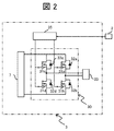
- FIG. 2 shows a schematic configuration of the small conversion devices 3, 4, 5, 6 constituting the power conversion device 1 of the power supply device 1 of FIG.
- FIG. 2 shows only the configuration of the small conversion device 3.
- the small converter 3 includes a switching circuit, an AC side connection terminal 33 electrically connected to the switching circuit, and a DC side connection terminal 7 connected to the power storage device 14.
- the switching circuit includes switching elements 31a, 31b, 31c, and 31d that are MOSFETs (Metal Oxide Semiconductors Field Effect Transistors).
- MOSFETs Metal Oxide Semiconductors Field Effect Transistors
- switching elements 31a, 31b, 31c, and 31d In the present embodiment, the case where a MOFET is used as the switching elements 31a, 31b, 31c, and 31d will be described as an example. However, other switching elements such as IGBT (Insulated Gate Bipolar Transistor) may be used. .
- IGBT Insulated Gate Bipolar Transistor
- the switching circuit includes a first arm configured by electrically connecting the source of the switching element 31a of the upper arm and the drain of the switching element 31b of the lower arm in series, and the switching element of the upper arm.
- a second arm configured such that the source of 31c and the drain of the lower arm switching element 31d are electrically connected in series, and the drains of the upper arm switching elements 31a and 31c and the lower arm switching element.
- Parasitic diodes are provided between the drains and the sources of the switching elements 31a, 31b, 31c, and 31d due to the structure of the MOSFETs. Specifically, a diode 32a is provided between the drain and source of the switching element 31a, a diode 32b is provided between the drain and source of the switching element 31b, and a diode is provided between the drain and source of the switching element 31c. The diode 32d is provided between the drain and the source of the switching element 31d. For this reason, it is not necessary to separately provide a diode between the drain and the source of the switching element. When an IGBT is used as the switching element, it is necessary to provide a diode between the drain and source of the switching element.
- the drains of the switching elements 31a and 31c of the upper arm are electrically connected to the positive electrode side of the DC connection terminal 34 as a DC positive electrode connection end.
- the sources of the lower-arm switching elements 31 b and 31 d are electrically connected to the negative electrode side of the DC side connection terminal 34.
- the middle point of the first arm that is, the electrical connection point between the source of the switching element 31a of the upper arm and the drain of the switching element 31b of the lower arm, and the middle point of the second arm, that is, the switching element 31c of the upper arm
- the electrical connection point between the source and the drain of the lower-arm switching element 31d is drawn out as an AC side connection terminal (load side connection end).
- An AC side connection terminal 33 is provided at the tip of each AC side connection terminal (load side connection end) of each of the first arm and the second arm. Of the two AC side connection terminals 33, one AC side connection terminal 33 is electrically connected to the AC side connection terminal 2 of the power converter 1. The other AC side connection terminal 33 is electrically connected to one of the AC side connection terminals of the small conversion device 4 that is electrically connected to the small conversion device 3 in series.
- the small conversion device 3 includes a control device 35.
- the control device 35 switches the switching elements 31a, 31b, 31c, and 31d so that the command voltage transmitted from the central control device 2 is linked to the power source connected to the power source side AC terminal 17 to which the power conversion device 7 is connected. Is controlled. For this reason, the control device 35 inputs the command voltage and the voltage level signal-transmitted from the central control device 2, and the switching elements 31a, 31b, 31c based on the input information and the stored information stored in advance. , 31d is calculated according to a drive pattern control program for switching (ON, OFF). And the control apparatus 35 produces
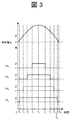
- FIG. 3 a calculation method of a command signal transmitted from the central control device 2 to the small conversion devices 3, 4, 5, 6 when the AC power supply system is connected to the system side connection terminal 13 is shown.
- the horizontal axis represents time
- the vertical axis represents the command voltage calculated by the central controller 2
- the basic voltage pattern V 0 3 of the AC side connection terminal of the small converter 3 and the AC side connection of the small converter 4.
- the basic voltage pattern V0 4 of the terminal, the basic voltage pattern V0 5 of the AC side connection terminal of the small converter 5 and the basic voltage pattern V0 6 of the AC side connection terminal of the small converter 6 are shown. .
- Central controller 2 calculates a command voltage based on the AC voltage of AC power supply system 18 connected to system side connection terminal 13 and the operating states of power storage devices 14, 15, 16, and 17. Based on the calculated command voltage, in the period from time 0 to time T 9 , the basic voltage pattern V 0 3 of the small converter 3 is made positive in the period from time T 1 to time T 8 according to the phase of the command voltage, basic voltage pattern V0 4 to be positive period of the small converter 4 time T 7 from the time T 2, from time T 3 to time period of the time T 6 the basic voltage pattern V0 5 small converter 5 is positive, the time T 4 from the basic voltage pattern V 0 6 small converter 6 for a period of time T 5 by the positive, but otherwise indicated in the drawings, the AC-side connection terminal of the basic voltage patterns each size converter to a positive period In addition, a voltage connected to the DC side connection terminal is applied to generate a multi-level voltage at the serial connection end 11.
- FIG. 3 shows an outline of the operation only when the command voltage is positive.
- the operation is the same as described above, but a command with the positive / negative sign reversed is transmitted.
- FIG. 4 is a control block diagram showing an outline of the algorithm of the power storage device charging state control means mounted on the central control device 2.
- the power storage device charge state control is configured by a basic voltage pattern calculation unit 201, a target power amount calculation unit 202, a correction voltage pattern calculation unit 203, and a final voltage pattern calculation unit 204.
- the basic voltage pattern calculation means 201 is a state of the AC power supply system 18, more specifically, the system voltage Vg estimated from the output signal of the voltage sensor, the AC current Ig estimated from the output signal of the current sensor, and the target power amount.
- the basic voltage pattern signal V0 i is calculated based on the target power amount Eet i carried by each small converter calculated by the calculation means 202.
- i is an integer indicating the number of the small conversion device.
- the basic voltage pattern calculation means 201 is based on the system voltage Vg and the system current Ig, and the command as shown in FIG. 3 is realized so as to realize the power that the power conversion device 1 transmits / receives to the system AC power supply system 18. Calculate the voltage.
- the basic voltage pattern calculation means 201 calculates the basic voltage pattern of the alternating current side connection terminals of the small converters 3, 4, 5, 6 based on the above-described command voltage in the form as shown in FIG. Further, the basic voltage pattern calculation unit 201 determines which small conversion device the basic voltage pattern is assigned to based on the target power amount Eet k calculated by the target power amount calculation unit 202, and finally determines the basic voltage pattern. Determine V0 i .
- k is an integer indicating the number of the power storage device. More specifically, when the target electric energy EEt k is small, a basic voltage pattern having a relatively short positive period is assigned among the patterns shown in FIG. When the target power amount EEt k is large, a basic voltage pattern having a relatively long positive period is assigned among the basic voltage patterns shown in FIG.
- the target power amount calculation means 202 includes a charge capacity ratio AhCR k that is a ratio of charge capacities of the power storage devices 14, 15, 16, and 17, an SOC ratio SOCR k that is a ratio of SOC (State Of Charge) that is in a charged state, and Based on an internal resistance ratio SOH k that is a ratio of internal resistance indicating the state of health (hereinafter referred to as SOH) of the power storage device, the target electric energy EEt k is calculated.
- k is an integer indicating the number of the power storage device.
- the power storage devices 14, 15, 16, and 17 are provided with a state management device, and the state control device provides the central controller 2 with a charge capacity AhC k indicating SOC, SOC k indicating SOC, And SOH k indicating the internal resistance is transmitted.
- the charge capacity ratio AhCR k is calculated by dividing AhC k by the sum of charge capacity values obtained by adding all the numbers of AhC k indicating the charge capacity.
- the SOC ratio SOCR k is calculated by dividing SOC k by the total SOC value obtained by adding all the numbers of SOC k indicating SOC.
- the internal resistance ratio SOHR k is calculated by dividing SOH k by the total internal resistance value obtained by adding the total number of SOH k indicating the internal resistance.
- the target power amount calculation unit 202 when the operation state of the power conversion device 1 transmits power, the target power amount calculation unit 202 is configured to reduce the power sharing amount of the power storage device having a small charge capacity ratio AhCR k. Reduce the electric energy EEt k .
- the target power amount EEt k is decreased in order to reduce the power sharing amount of the power storage device having a small SOC ratio SOCR k .
- the target power amount EEt k is set small in order to reduce the power sharing amount of the power storage device having a large internal resistance ratio SOHR k .
- the target power amount EEt k is set large. Note that the target power amount is a value obtained by integrating the power of a quarter period in the period of one cycle of the command voltage shown in FIG.
- the correction voltage pattern calculation means 203 is based on the basic voltage pattern V0 i , the alternating current Ig, the terminal voltage VBAT k of the power storage device, and the target electric energy Eet k that are the outputs of the basic voltage pattern calculation means 201.
- the correction voltage patterns Vd i of 4, 5, 6 are calculated.
- the correction voltage pattern calculation means 203 calculates a correction voltage pattern based on the target electric energy EEt k , the correction voltage pattern Vd i , the storage battery voltage VBAT i, and the alternating current Ig as its calculation result.
- the difference between the amount of power and the target electric energy EET k when reflecting sequentially monitors calculates a correction voltage pattern on the basis of this difference. A specific operation example will be described later.
- the final voltage pattern calculation means 204 calculates the final voltage pattern V i of the small converters 3, 4, 5, 6 based on the basic voltage pattern V0 i and the correction voltage pattern Vd i . More specifically, the final voltage pattern V0 i is calculated by adding the basic voltage pattern V0 i and the correction voltage pattern Vd i .
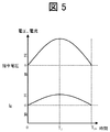
- FIG. 5 it is assumed that the operating state of the power conversion device 1 transmits power from the power storage devices 14, 15, 16, and 17 to the AC power supply system 18.
- the horizontal axis indicates time
- the vertical axis indicates the command voltage and the alternating current Ig from the upper side of the figure, and the voltage is positive and the current is positive toward the upper side of the figure.
- the power converter 1 is in an operating state in which power is transmitted from the power storage devices 14, 15, 16, and 17 to the alternating current power supply system 18. .
- FIG. 6 shows the electric energy EE k of the power storage devices 3, 4, 5, and 6 connected to the power conversion device 1 when the power storage device charging state control described in the present embodiment is not applied.
- k is an integer indicating the number of the power storage device.
- the horizontal axis of FIG. 6 shows a power storage unit number, and the vertical axis indicates the amount of power EE k of the power storage device, respectively, indicating that the FIG upward large amount of power.
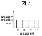
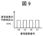
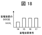
- FIGS. 7, 8, and 9 show the charge capacity ratio AhCR k , SOC ratio SOCR k , and internal resistance ratio SOHR k of the power storage device in the present embodiment
- the horizontal axis indicates the power storage device number
- the vertical axis indicates The charge capacity ratio AhCR k , SOC ratio SOCR k , and internal resistance ratio SOHR k of the power storage device are respectively shown.
- the charge capacity ratio AhCR k , the SOC ratio SOCR k , and the internal resistance ratio SOHR k are in the states shown in FIGS. 7, 8, and 9, respectively. Even if it exists, as shown in FIG. 3, the period when the voltage pattern of the small converters 3, 4, 5, and 6 is positive is commanded. Therefore, since there is a difference in the positive period of the voltage pattern, as shown in FIG. 6, the amount of power carried by the power storage device with a small power storage device number is reduced. Thereby, since the states of the power storage devices 14, 15, 16, and 17 change, the life of the storage battery number 6 becomes relatively short, and dominates the life of the power storage system.
- the state of the power storage device can be maintained substantially equal by the following procedure.
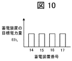
- FIG. 10 shows the state of charge of the power storage device of the present embodiment when the states of the charge capacity ratio AhCR k , SOC ratio SOCR k , and internal resistance ratio SOHR k shown in FIGS. 7, 8, and 9 are substantially equal.
- the target power amount EEt k calculated by the control target power amount calculation means 202 is shown.
- the horizontal axis in FIG. 10 indicates the power storage device number, and the vertical axis indicates the target power amount of the power storage devices 13, 14, 15, and 16.
- the target power amount calculation means 202 determines that the amount of power carried by the power storage device needs to be equalized, and is shown in FIG. Thus, the target electric energy EEt k is set to be approximately equal.
- FIG. 11 is a diagram showing an example of the operation of the correction voltage pattern calculation unit 203 shown in FIG.
- the horizontal axis of FIG. 11 indicates time, and the vertical axis indicates the command voltage, the alternating current Ig, the correction voltage pattern Vd 3 of the small converter 3 , the correction voltage pattern Vd 4 of the small converter 4 , and the small converter 5 from the top of the figure.
- the correction voltage pattern Vd 5 indicates indicates that the voltage upward in Fig positive, current is positive.
- the correction voltage pattern calculating unit 203 shows the power amount EE i borne by the power storage device in the basic voltage pattern shown in FIG.
- the correction voltage pattern Vd i is calculated so as to coincide with the target power amount EEt k shown. More specifically, in the period from time 0 to time T 5 , the correction voltage pattern Vd of the small converter 3 is increased in the period from time T 1 to time T b in order to increase the amount of power EE 14 of the power storage device 14.
- the power storage device in order to increase the amount of power EE 15 of 15, the correction voltage pattern Vd 4 positive urban small converter 4 during a period from time T 2 to time T a, the power amount of the power storage device 16 in order to reduce the EE 16, the correction voltage pattern Vd 5 small converter 5 as a negative in the period from time T 2 to time T a, in order to reduce the amount of power EE 17 of the storage device 17, the time T 1 period from to time T b at which the correction voltage pattern Vd 6 small converter 6 and negative.
- a correction voltage pattern Vd 3 small converter 3 during a period from time T 6 to time T c positive
- the correction voltage pattern Vd 4 of the small conversion device 4 is made positive in the period from the time T 7 to the time T d
- the electric energy EE 16 of the power storage device 16 is
- the correction voltage pattern Vd 5 of the small conversion device 5 is made negative in the period from the time T 7 to the time T d
- the correction voltage pattern Vd 6 of the small converter 6 is negative.
- the magnitude of the correction voltage pattern in the positive and negative direction is determined based on VBAT k that is the terminal voltage of power storage devices 14, 15, 16, and 17.
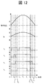
- FIG. 12 is a diagram showing an example of the operation of final voltage pattern calculation means 204 shown in FIG.
- the horizontal axis of FIG. 12 indicates time, and the vertical axis indicates the command voltage, the alternating current Ig, the final voltage pattern V 3 of the small conversion device 3 , the final voltage pattern V 4 of the small conversion device 4 , and the small conversion device 5 from the top of the drawing.
- final voltage pattern Vd 5 of the final voltage pattern V 6 of the small converter 6 indicates indicates that the voltage upward in Fig positive, current is positive.
- the final voltage pattern calculation unit 204 adds the correction voltage pattern Vd i output from the correction voltage pattern calculation unit 203 to the basic voltage pattern V0 i output from the basic voltage pattern calculation unit 201.
- the final voltage pattern V i is determined. More specifically, in order to increase than for the electric energy EE 14 of the electric storage device 14 only the basic voltage pattern V0 3 shown in FIG. 3, the time from the time and time T 4 from time T 1 to time T c T the final voltage pattern V 3 is positive small converter 3 at a time to c, in order to increase than for the electric energy EE 15 of the electric storage device 15 only the basic voltage pattern V0 4 shown in FIG.
- time T 2 basic voltage pattern indicating a final voltage pattern V 4 small converter 4 in the period from the period and time T 3 to time T a to time T d is positive
- the electric energy EE 17 of 17 in order to reduce than when only the basic voltage pattern V 6 shown in FIG. 3
- the final voltage pattern V 6 of the small converter 6 in the period from the period and time T c from between T b to time T 6 to time T 9 is positive.
- the power storage device charging state control according to the present embodiment is based on the state of the power storage device 1, and by sequentially correcting and distributing the voltage pattern from the basic voltage pattern of the small converter shown in FIG. It is possible to control this state to a suitable state.
- FIG. 5 the operation state in the case where power is transmitted from the power storage devices 14, 15, 16, and 17 to the AC power supply system 18 has been described, but the state of the power storage devices 14, 15, 16, and 17 is described.
- FIG. 8 and FIG. 9 when the power storage devices 3, 4, 5, 6 receive power from the AC power supply system 18,
- the voltage patterns of the small converters 14, 15, 16, and 17 are the same as those in FIG. 13, the horizontal axis indicates time, and the vertical axis indicates the command voltage, the alternating current Ig, the final voltage pattern V 3 of the small conversion device 3 , and the final voltage of the small conversion device 4 from the top of the drawing, as in FIG.
- a pattern V 4 , a final voltage pattern Vd 5 of the small conversion device 5 , and a final voltage pattern V 6 of the small conversion device 6 are shown, and the voltage is positive and the current is positive toward the top of the figure.
- the power storage device charging state control in the present embodiment is performed regardless of the operating state of the power converter 1, that is, regardless of the direction of power transmission / reception between the power storage devices 14, 15, 16, 17 and the AC power supply system 18.
- the voltage patterns of the small converters 3, 4, 5, 6 are distributed so that the charge capacity ratio reciprocal sequence, which is a sequence in which the reciprocals are arranged in ascending order, is substantially equivalent.
- the power amount ratio sequence that is a numerical sequence in which the power amounts EE k of the power storage devices 14, 15, 16, and 17 are arranged in ascending order and the SOCR k that is the SOC ratio are small.
- the voltage of the small converters 3, 4, 5, 6 so that the SOC ratio sequence which is a sequence arranged in order or the SOC ratio reciprocal sequence which is a sequence obtained by arranging the reciprocals of the SOC ratio SOCR k in ascending order is almost equal. Distribute the pattern. Furthermore, in the power storage device charge state control in the present embodiment, the power amount ratio sequence, which is a numerical sequence in which the power amounts EE k of the power storage devices 14, 15, 16, and 17 are arranged in ascending order, and the internal resistance ratio SOHR i are arranged in ascending order.
- FIG. 14 to FIG. 23 a power storage device charge state control for controlling the charge states of the power storage devices 14, 15, 16, and 17 constituting the power storage system to which the power conversion device 1 of this embodiment is applied. An operation state different from the above-described means will be described.
- the charge capacity ratio AhCR k of power storage devices 14, 15, 16, and 17 shows charge capacity ratio charge AhCR k of power storage devices 14, 15, 16, and 17, and the horizontal axis shows the power storage device number as in FIG. 7, and the vertical axis shows charge capacity ratio charge AhCR k of the power storage device.
- the upper part of the figure is positive.
- k is an integer indicating the number of the power storage device.
- the charge capacity ratio AhCR k of the power storage devices 14, 15 , 16 , and 17 is low as shown in FIG. 14, and the AhCR 14 of the power storage devices 15 , 16 , and 17 is low.
- AhCR 17 is larger than AhCR 14 of power storage device 14 and power storage devices 15, 16, and 17 are substantially equivalent.
- FIG. 15 shows the states of the charge capacity ratio AhCR k , SOC ratio SOCR k , and internal resistance ratio SOHR k of the power storage devices 14, 15, 16, and 17, respectively, as shown in FIGS. 14, 8, and 9. case, indicates the target amount of power EET k of the power storage device 14, 15, 16, 17 to the target electric energy computing means 202 of the power storage device charged state control means of the present embodiment shown in FIG. 4 is computed.
- the horizontal axis of FIG. 15 shows a power storage unit number, and the vertical axis represents the target electric energy EET k of the power storage device.
- the target power amount indicates a value obtained by integrating the power in a quarter cycle period in one cycle of the command voltage.
- the states of charge capacity ratio AhCR k , SOC ratio SOCR k , and internal resistance ratio SOHR k of power storage devices 14, 15, 16, and 17 are shown in FIG. 4 in the states of FIGS. 14, 8, and 9, respectively.
- the target power amount calculation means 202 of the power storage device charging state control means of the present embodiment is shown when the operating state of the power conversion device 1 transmits power from the power storage devices 14, 15, 16, 17 to the AC power supply system 18. Since the charge capacity ratio AhCR k of the power storage device 14 is small, as shown in FIG. 15, the target power amount ratio Eet i is calculated so that the amount of power carried by the power storage device 14 is smaller than that of other power storage devices.
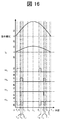
- FIG. 16 shows the states of the charge capacity ratio AhCR k , SOC ratio SOCR k , and internal resistance ratio SOHR k of the power storage devices 14, 15, 16, and 17 in the states shown in FIGS. 14, 8, and 9, respectively. It is the figure which showed an example of the operating state of the correction voltage pattern calculating means 203 of this embodiment.
- the horizontal axis of FIG. 16 indicates time, and the vertical axis indicates the command voltage, the alternating current Ig, the final voltage pattern Vd 3 of the small converter 3 , the final voltage pattern Vd 4 of the small converter 4 , and the small converter 5 from the top of the figure.
- final voltage pattern Vd 5 of the final voltage pattern Vd 6 small converter 6 indicates indicates that the voltage upward in Fig positive, current is positive.
- the correction voltage pattern calculating unit 203 shows the power amount EE k carried by the power storage device in the basic voltage pattern shown in FIG.
- the correction voltage pattern Vd i is calculated so as to coincide with the target power amount EEt k shown.
- the power amount EE 14 of the power storage device 14 is increased, but in order to make the power amount EE 14 smaller than the power storage devices 15, 16, 17,
- the correction voltage pattern Vd 3 of the small conversion device 3 is made positive, and the power amount EE 15 of the power storage device 15 is increased, but is larger than the power amount EE 14 of the power storage device 14 Therefore , in the period from time T 2 to time T c2 , the correction voltage pattern Vd 4 of the small conversion device 4 is made positive and the power amount EE 16 of the power storage device 16 is reduced, but the power amount is higher than that of the power storage device 14.
- the power amount EE 14 of the power storage device 14 is increased, but in order to make the power amount EE 14 smaller than the power storage devices 15, 16, 17, the time T 6 small converter 3 of the correction voltage pattern Vd 3 to be positive in the period up to the time T d2 from increases the amount of power EE 15 of the power storage device 15, for a greater state than the power amount EE 14 of the electric storage device 14 Furthermore, the correction voltage pattern Vd 4 of the small conversion device 4 is made positive in the period from the time T 7 to the time T f2, and the power amount EE 16 of the power storage device 16 is decreased, but the power amount EE 14 of the power storage device 14 is decreased.
- a correction voltage pattern Vd 5 small converter 5 as a negative in the period from time T 7 to time T e3, power of the power storage device 17
- the amount EE 17 is reduced, while being larger than the power amount EE 14 of the power storage device 14
- To the electric energy EE 15 and EE 16 of the power storage device 15 and the power storage device 16 are approximately equal to, small conversion and from time T 6 to time T d2, and from time T e2 until time T f2 a correction voltage pattern Vd 6 of the device 6 to be negative.
- the magnitude of the correction voltage pattern in the positive and negative direction is determined based on VBAT k that is the terminal voltage of power storage devices 14, 15, 16, and 17.
- the small-sized conversion device in the period from time 0 to time Ta 2 than the base voltage pattern V0 6 of 17, it calculates a and Vd 6 correction voltage pattern Vd 3 to switch the positive voltage period to the basic voltage pattern V0 3 small converter 3.
- increasing the amount of power EE 15 of the power storage device 15, in order to reduce the amount of power EE 16 of the power storage device 16, from the basic voltage pattern V0 5 small converter 5 during a period from time T 2 to time T b2 calculates a correction voltage pattern Vd 4 and Vd 5 to switch the positive voltage period to the basic voltage pattern V0 4 small converter 4. Furthermore, increasing the amount of power EE 15 of the power storage device 15, in order to reduce the amount of power EE 17 of the storage device 17, from the basic voltage pattern V0 6 small converter 6 during a period from time T b to time T c2 calculates a and Vd 6 corrected voltage pattern Vd 4 to replace the positive voltage period to the basic voltage pattern V0 4 small converter 4.
- the correction voltage patterns Vd 3 and Vd 6 are calculated from the basic voltage pattern V 0 6 of the small conversion device 17 so that the positive period of the voltage is switched to the basic voltage pattern V 0 3 of the small conversion device 3.
- increasing the amount of power EE 15 of the power storage device 15, in order to reduce the amount of power EE 16 of the power storage device 16, from the basic voltage pattern V0 5 small converter 5 during a period from time T 7 to time T e2 calculates a correction voltage pattern Vd 4 and Vd 5 to switch the positive voltage period to the basic voltage pattern V0 4 small converter 4. Furthermore, increasing the amount of power EE 15 of the power storage device 15, in order to reduce the amount of power EE 17 of the storage device 17, from the basic voltage pattern V0 6 small converter 6 during a period from the time T e2 until time T f2 calculates a and Vd 6 correction voltage pattern Vd 3 to switch the positive voltage period to the basic voltage pattern V0 4 small converter 4.
- FIG. 17 is a diagram showing an example of the operation of final voltage pattern calculation means 204 shown in FIG.
- the horizontal axis of FIG. 16 indicates time, and the vertical axis indicates the command voltage, the alternating current Ig, the final voltage pattern V 3 of the small conversion device 3 , the final voltage pattern V 4 of the small conversion device 4 , and the small conversion device 5 from the top of the drawing.
- the final voltage pattern V 5 of the final voltage pattern V 6 of the small converter 6 indicates indicates that the voltage upward in Fig positive, current is positive.
- the final voltage pattern calculation unit 204 adds the correction voltage pattern Vd i output from the correction voltage pattern calculation unit 203 to the basic voltage pattern V0 i output from the basic voltage pattern calculation unit 201.
- the final voltage pattern V i is determined. More specifically, but increases than in the electric energy EE 14 of the electric storage device 14 only the basic voltage pattern V0 3 shown in FIG. 3, to be smaller than the power quantity of the power storage device 15, 16, 17 hours basic indicating the final voltage pattern V 3 of the small converter 3 in the period from the period and time T 4 from T 1 to time T c to time T d2 is positive, the amount of power EE 15 of the power storage device 15 in FIG.
- the final voltage pattern V 6 of the small converter 6 is positive.
- the power storage device charging state control according to the present embodiment is based on the state of the power storage device 1, and by sequentially correcting and distributing the voltage pattern from the basic voltage pattern of the small converter shown in FIG. It is possible to control this state to a suitable state.
- the states of the charge capacity ratio AhCR k , SOC ratio SOCR k , and internal resistance ratio SOHR k of the power storage devices 14, 15, 16, and 17 take the forms shown in FIGS. 14, 8, and 9, respectively.
- the operation state of the power conversion device 1 is a case where power is transmitted from the power storage devices 14, 15, 16, 17 to the AC power supply system 18.
- the target power amount Eet k calculated by the target power amount calculating means 202 is as shown in FIG. 15, and as a result, the charge capacity ratio AhCR k of the power storage devices 14, 15, 16, and 17 is calculated.
- the amount of power EE k small and trends watt ratio sequence is a sequence obtained by arranging in the order of approximately equal become so small transducers 3, 4, 5, 6 Distribute voltage patterns.
- the SOCR 14 of the power storage device 14 in the SOC ratio SOCR k of the power storage device shown in FIG. The power storage devices 15, 16, and 17 have almost the same SOCR k , and the charge capacity ratio AhCR k and the internal resistance ratio SOHR k are substantially the same as shown in FIGS. 7 and 9, respectively. There is.
- the tendency of the charge capacity ratio which is a numerical sequence in which the SOC ratio SOCR k of the power storage devices 14, 15, 16, 17 is arranged in ascending order
- the tendency of the electric energy ratio sequence which is a numerical sequence in which the electric energy EE k is arranged in ascending order.
- the SOCH 14 of the power storage device 14 is the power storage device 15, 16 and 17, and the power storage devices 15, 16, and 17 have substantially the same SOHR k , and the states of the charge capacity ratio AhCR k and the SOC ratio SOCR k are substantially the same as shown in FIGS. 7 and 8, respectively.
- the tendency of the internal resistance ratio reciprocal sequence which is a sequence in which the reciprocals of the SOC ratio SOHR k of the power storage devices 14, 15, 16, 17 are arranged in ascending order, and the electric energy that is the sequence in which the electric energy EE k is arranged in ascending order.
- the voltage patterns of the small converters 3, 4, 5, 6 are distributed so that the tendency of the ratio sequence is almost equal.
- FIG. 23 an example of operation when the power storage devices 14, 15, 16, and 17 receive power from the AC power supply system 18 will be described.
- FIG. 20 is an example of a calculation result of the target power amount calculation unit 202 when the power storage devices 14, 15, 16, and 17 receive power from the AC power supply system 18.
- the horizontal axis of FIG. 20 shows a power storage unit number, and the vertical axis represents the target electric energy EET k of the power storage device.
- the charge capacity ratio AhCR k , SOC ratio SOCR k , and internal resistance ratio SOHR k of power storage devices 14, 15, 16, and 17 are as shown in FIGS. 14, 8, and 9, respectively, and only AhCR 14 of power storage device 14 is In a situation where the power storage devices 15, 16, and 17 have substantially the same AhCR k and the SOC ratio SOCR k and the internal resistance ratio SOHR k are substantially the same in all power storage devices, the target power amount calculation means 202 In order to relatively increase the amount of power charged by the power storage device 14, the target power amount EEt k of the power storage devices 14, 15, 16, and 17 is only the power amount Eet 14 of the power storage device 14 as shown in FIG. Enlarge.
- the power amount calculation means 202 sets the target power amount EEt k of the power storage devices 14, 15, 16, and 17 as shown in FIG. 20. Only increase the electric energy EET 14 .
- the charge capacity ratio AhCR k , SOC ratio SOCR k , and internal resistance ratio SOHR k of the power storage devices 14, 15, 16, and 17 are as shown in FIGS. 7, 8, and 19, respectively. Only the ratio SOHR k is small, the internal resistance ratios SOHR k of the power storage devices 15, 16, and 17 are almost equal, and the charge capacity ratio AhCR k and the SOC ratio SOCR k are almost equal in all power storage devices
- the target power amount calculation means 202 stores the target power amount Eet k of the power storage devices 14, 15, 16, and 17 as shown in FIG. 20 in order to relatively increase the amount of power charged by the power storage device 14. only electric energy EET 14 of device 14 is increased.
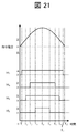
- FIG. 21 illustrates an operation example of the basic voltage pattern calculation unit 201 when the power storage devices 14, 15, 16, and 17 receive power from the AC power supply system 18.
- the basic voltage patterns of the small conversion device 3 and the small conversion device 6 are exchanged from the basic voltage pattern of FIG.
- FIG. 22 is a diagram illustrating an operation example of the correction voltage pattern calculation unit 203 when the target electric energy EEt k takes the form shown in FIG. 20 and the basic voltage pattern V0 i takes the form shown in FIG.
- the horizontal axis of FIG. 22 indicates time, and the vertical axis indicates the command voltage, the alternating current Ig, the final voltage pattern Vd 3 of the small converter 3 , the final voltage pattern Vd 4 of the small converter 4 , and the small converter 5 from the top of the figure.
- final voltage pattern Vd 5 of the final voltage pattern Vd 6 small converter 6 indicates indicates that the voltage upward in Fig positive, current is positive.
- the phase difference between the command voltage Vg and the alternating current Ig is 180 degrees. This is an example of the case where the power storage devices 14, 15, 16, and 17 receive power from the alternating current power supply system 18. Yes.
- the correction voltage pattern calculation means 203 calculates the correction voltage pattern Vd i so that the amount of power EE k carried by the power storage device in the basic voltage pattern shown in FIG. 21 matches the target power amount EEt k shown in FIG. More specifically, in the period from time 0 to time T 5 , the correction voltage pattern Vd of the small-sized conversion device 3 in the period from time T 1 to time Ta 3 in order to decrease the electric energy EE 14 of the power storage device 14.
- the correction voltage pattern Vd 4 of the small-sized conversion device 4 is made negative in the period from the time Tc2 to the time Tc2, and the power amount EE 16 of the power storage device 16 is decreased, but is smaller than the power amount EE 14 of the power storage device 14 and
- the correction voltage pattern Vd 5 of the small conversion device 5 is made negative in the period from the time Ta 3 to the time T b3 to increase the power amount EE 17 of the power storage device 17 so as to be almost equal to the power amounts 15 and 17 .
- a correction voltage pattern Vd 6 small converter 6 to be positive in the period from time T 1 to time T c3.
- a negative correction voltage pattern Vd 3 small converter 3 during a period from time T 6 to time T d3
- the power amount EE 15 of the power storage device 15 is increased, but in order to be larger than the power amount EE 14 of the power storage device 14 and substantially equal to the power amounts of the power storage devices 16 and 17, the time T e3 to the time T
- the correction voltage pattern Vd 4 of the small-sized conversion device 4 is set to be negative and the power amount EE 16 of the power storage device 16 is reduced, but while being smaller than the power amount EE 14 of the power storage device 14,
- the correction voltage pattern Vd 5 of the small converter 5 is made negative in the period from the time T d3 to the time Te 3 and in the period from the time T 7 to the time T f3 so as to be almost equal to the electric energy of 17.
- the magnitude of the correction voltage pattern in the positive and negative direction is determined based on VBAT k that is the terminal voltage of power storage devices 14, 15, 16, and 17.
- the small conversion device In the period from time 0 to time T 5 , in order to decrease the power amount EE 14 of the power storage device 14 and increase the power amount EE 17 of the power storage device 17, the small conversion device is used in the period from time T 1 to time Ta 3. than the base voltage pattern V0 3 of 3, it calculates a and Vd 6 correction voltage pattern Vd 3 to switch the positive voltage period to the basic voltage pattern V0 6 small converter 6.
- the correction voltage patterns Vd 3 and Vd 6 are calculated from the basic voltage pattern V 0 3 of the small conversion device 3 so that the positive period of the voltage is switched to the basic voltage pattern V 0 6 of the small conversion device 6.
- FIG. 23 is a diagram illustrating an example of the operation of the final voltage pattern calculation unit 204.
- the horizontal axis indicates time, and the vertical axis indicates the command voltage, the alternating current Ig, the final voltage pattern V 3 of the small conversion device 3 , the final voltage pattern V 4 of the small conversion device 4 , and the small conversion device 5 from the top of the drawing.
- the final voltage pattern V 5 of the final voltage pattern V 6 of the small converter 6 indicates indicates that the voltage upward in Fig positive, current is positive.
- the final voltage pattern calculation unit 204 adds the correction voltage pattern Vd i output from the correction voltage pattern calculation unit 203 to the basic voltage pattern V0 i output from the basic voltage pattern calculation unit 201.
- the final voltage pattern V i is determined. More specifically, in order to decrease than for the electric energy EE 14 of the electric storage device 14 only the basic voltage pattern V0 3 shown in FIG. 21, the time from the time and time T d3 from time T a3 to time T 6 T In the period up to 9, the final voltage pattern V 3 of the small-sized conversion device 3 is positive, and the electric energy EE 15 of the power storage device 15 is reduced as compared with the case of only the basic voltage pattern V 0 4 shown in FIG.
- the final voltage pattern V 6 of the small converter 6 is positive in the period from the time T 1 to the time T c3 and in the period from the time T 4 to the time T f3 in order to make it almost equal to the electric energy of 15 and 16.
- the charge state control of the power storage device of the present embodiment is performed by correcting and distributing the voltage pattern sequentially from the basic voltage pattern of the small converter shown in FIG. 3 based on the state of the power storage device 1. Even when the devices 14, 15, 16, and 17 receive power from the AC power supply system 18, it is possible to control the state of the power storage device to a suitable state.
- the reciprocal of the charge capacity ratio AhCR k of the power storage devices 14, 15, 16, and 17 is determined by the power storage device charge state control of the present embodiment.
- the reciprocal sequence of charge capacity ratio which is a sequence of numbers arranged in ascending order
- the tendency of the power amount ratio which is a sequence of numbers of power amounts EE k of power storage devices 14, 15, 16, and 17, arranged in ascending order.
- the SOC ratio reciprocal sequence which is a sequence in which the reciprocals are arranged in ascending order
- the tendency of the electric energy ratio which is a sequence in which the power amounts EE k of the power storage devices 14, 15, 16, 17 are arranged in ascending order, are substantially equal.
- the internal resistance ratio sequence which is a number sequence in which SOHR k is arranged in ascending order
- the power amount ratio tendency which is a sequence in which the power amounts EE k of power storage devices 14, 15, 16, and 17 are arranged in ascending order
- the charge capacity ratio AhCR k , the SOC ratio SOCR k , and the internal resistance ratio SOHR k that are the states of the power storage devices 14, 15, 16, and 17 are each one and only one power storage device.
- the present invention is not limited to this, and the power storage device charging state control according to the present embodiment is not limited to this.
- SYMBOLS 1 Power converter device, 2 ... Central controller, 3, 4, 5, 6 ... Small converter device, 7, 8, 9, 10 ... DC power supply side connection terminal, 11 ... Series connection end, 12 ... interconnection reactor, 13 ... system side connection terminal, 14, 15, 16, 17 ... power storage device, 18 ... single phase AC power supply system, 33 ... AC side Connection terminal, 35... Control device.
Landscapes
- Engineering & Computer Science (AREA)
- Power Engineering (AREA)
- Charge And Discharge Circuits For Batteries Or The Like (AREA)
Abstract
本発明の目的は、直流と交流とを変換可能であると共に、直流側に接続した蓄電装置の寿命を長期化可能な蓄電システム向けの電力変換装置を提供することにある。 直流と交流とを変換する小型変換装置を複数備え、複数の蓄電装置を備え、複数の小型変換機のそれぞれの直流側に蓄電装置が接続され、複数の小型変換器の直流側が直列接続された電力変換装置であって、蓄電装置の状態に基づいて、小型変換器のPWM信号のオン期間を入れ替えることで、小型変換器の電力量を自在に変更する。
Description
本発明は、電力変換装置に関する。
例えば、特許文献1には、直流電源回路に接続された単相電力変換器を複数備え、単相電力変換器の交流出力端子を直列に接続した直列多重電力変換装置において、電圧指令に同期したPWM信号を演算する手段と、PWM信号が変化するタイミングを複数の単相電力変換器の間で入れ替えてこれらの単相電力変換器の電圧出力期間を均等化する手段とを備えた前記直列多重電力変換装置が開示されている.
特許文献2には、直流電源回路に接続された複数の単相電力変換器を備え、単相電力変換器の交流出力端を直列接続する直列多重電力変換器を制御するための制御装置であって、直列多重電力変換器に対する電圧指令を発生する手段と、電圧指令から単相電力変換器の半導体素子をスイッチングするためのPWM信号を発生する手段と、を備えた制御装置において、電圧指令の大きさに応じて複数のPWM信号を複数の単相電力変換器に分配する手段を有し、各単相電力変換装器のよる電力分担を均等化させることを特徴とする多重電力変換器の制御装置が開示されている.
特許文献2には、直流電源回路に接続された複数の単相電力変換器を備え、単相電力変換器の交流出力端を直列接続する直列多重電力変換器を制御するための制御装置であって、直列多重電力変換器に対する電圧指令を発生する手段と、電圧指令から単相電力変換器の半導体素子をスイッチングするためのPWM信号を発生する手段と、を備えた制御装置において、電圧指令の大きさに応じて複数のPWM信号を複数の単相電力変換器に分配する手段を有し、各単相電力変換装器のよる電力分担を均等化させることを特徴とする多重電力変換器の制御装置が開示されている.
近年、二酸化炭素の排出による地球温暖化や、化石燃料の枯渇が懸念されており、二酸化炭素の排出量の低減や、化石燃料への依存度の低下が求められている。二酸化炭素の排出量の低減や、化石燃料への依存度の低下を図るためには、風力や太陽光などの自然から得られる再生可能エネルギーを利用した発電システムの導入が有効であると考えられる。再生可能エネルギーを利用した発電システムの導入にあたっては、気象条件に左右される再生可能エネルギーの変動に伴う電力変動を抑制する手段が必要であり、その手段の一つとして、電気エネルギーの蓄積及び放出が可能な蓄電システムが注目されている。再生可能エネルギーに併設した際の蓄電システムの具体的な動作としては、再生可能エネルギーが発電する電力が余剰である場合には余剰電力を貯蔵し、電力が不足する際には不足電力を補うために蓄電システムから放電する。このように、再生可能エネルギー発電システムに蓄電システムを併設することにより、再生可能エネルギーを有効利用することが可能である。
再生可能エネルギーの発電システムに併設される蓄電システムは、比較的短いサイクルで充放電が繰り返されるため、蓄電システムを構成する蓄電装置の寿命管理が重要である。従来の蓄電システムは、インバータまたはパワーコンディショナを用いて蓄電装置をまとめて管理している。この場合、蓄電装置の特性ばらつきが主な要因で、一部の性能の低い蓄電装置が、周辺の良好な性能の蓄電装置に悪影響を及ぼすことで、蓄電システム全体の寿命が短期化するという問題がある。
蓄電システムの寿命を管理する好適な手段の一つとして、特許文献1、特許文献2に開示された技術のように、直流電源回路に接続された複数の単相電力変換器を備え、単相電力変換器の交流出力端を直列接続する直列多重電力変換器を、蓄電システムの電力変換器として採用することが考えられる。上記直列多重電力変換器を用いることにより、蓄電装置の状態を単相電力変換器毎に管理することが可能であることから、蓄電装置の寿命を長期化することが可能である。
特許文献1に開示されている直列多重電力変換器は、複数ある単相電力変換器が出力する電圧出力期間を均等化することで、複数の単相電力変換器の電力分担を均等化することが可能であるため、蓄電装置が同種であり、新品状態や劣化状態が同様である場合には有効である。ただし、種類が異なる蓄電装置を利用する場合や、同種ではあるが特性の異なる蓄電装置を利用する場合や、蓄電装置の特性ばらつきによって蓄電装置の性能に差異が生じた場合には、蓄電装置の状態に合わせて電力分担を調整することができないために、蓄電装置の状態を最適に管理できず、寿命を長期化できないのみならず、逆に短期化させるという課題があった。
また、特許文献2に開示された直列多重電力変換器の制御装置も同様に、複数の単相電力変換器の電力分担を均等化する技術であることから、上述と同様に、蓄電装置の状態に応じて電力分担を調整できず、蓄電装置の寿命を長期化できないという課題があった。
本発明の目的は、直流と交流とを変換可能であると共に、直流側に接続した蓄電装置の寿命を長期化可能な蓄電システム向けの電力変換装置を提供することにある。
電力変換装置は、直流と交流とを変換する単相フルブリッジ回路により構成される小型変換装置を複数備え、複数の蓄電装置を備え、前記小型変換装置の直流側接続端子に前記蓄電装置を接続しており、前記小型変換装置の前記交流側接続端子を直列接続し、前記小型変換装置の交流側接続端子に生成する電圧を合成することで交流電圧を生成する電力変換装置であって、前記小型変換装置の前記直流接続端子に接続する前記蓄電装置の充電容量をすべて加算した充電容量総和値により、前記蓄電装置の前記充電容量を除算した結果である充電容量比を、小さい順に並べた数列を充電容量比列とし、前記電力変換器が生成する前記交流電圧のサイクルである交流電圧サイクルのうち、前記交流電圧サイクルの4分の1の期間で前記小型変換装置が変換する電力を時間積分した小型変換装置の電力量を、前記小型変換装置の数だけ加算した電力量総和値にて、前記小型変換装置の電力量を除算した値である電力量比を、小さい順に並べた数列を電力量比列とすると、前記電力変換装置より電力を送電する運転条件において、前記充電容量比列の傾向と前記電力量比列との傾向がほぼ同等であることを特徴とする。
本発明によれば、直流と交流とを変換可能であると共に、直流側に接続した蓄電装置の寿命を長期化可能な蓄電システム向けの電力変換装置を提供することができる。
以下に説明する実施形態は、電力貯蔵や電力供給を目的とする蓄電システムの電力変換装置に適用できる。
また、以下に説明する実施形態は、小型変換装置の直流側接続端子にキャパシタを接続することにより、系統電圧の安定化を図る静止型無効電力補償装置の電力変換装置にも適用できる。
さらに、以下に説明する実施形態は、小型変換装置の直流側接続端子に、蓄電装置やキャパシタではなく、太陽電池パネルを接続することにより、太陽電池パネルで発電した直流電力を交流電力に変換する電力変換装置にも適用できる。
次に、電力変換装置の概略構成について、説明する。
電力変換装置は、直流電力を交流電力に変換したり、交流電力を直流電力に変換したりする装置である。電力変換装置の直流側接続端子に直流電力源を接続し、交流側接続端子にリアクトルを介して交流電源系統を接続、連系する場合がある。また、交流側接続端子に、発電機を代表とする交流負荷を接続する場合がある。
以下に説明する実施形態では、電力変換装置の直流側接続端子に蓄電装置を接続し、交流側接続端子にリアクトルを介して交流電源系統を接続し、連系動作を可能とする場合を例に挙げて説明する。
図面を用いて、本発明の実施形態について具体的に説明する。
まず、図1を用いて、本願に係る電力変換装置の実施形態の概略構成について説明する。図1は、本願の電力変換装置1を適用した蓄電システムの全体の概略構成を示す。
電力変換装置1は、一端の接続端子である系統側接続端子13を介して単相交流電源系統18と接続しており、直流電源側接続端子7、8、9、10を介して蓄電装置14、15、16、17と接続している。
本実施形態では、系統側接続端子12に単相交流電源系統18を接続した場合を例に挙げて説明しているが、発電機などの交流電源負荷を接続しても構わない。
また、電力変換装置1は、中央制御装置2、小型変換装置3、4、5、6、直流電源側接続端子7、8、9、10、連系リアクトル12、および系統側接続端子13を備えている。電力変換装置1の小型変換装置3、4、5、6の交流側接続端子は電気的に直列接続されており、小型変換装置3、4、5、6の直列接続端11より連系リアクトル12を介して系統側接続端子13に接続されている。また、小型変換装置3、4、5、6の直流側接続端子は直流電源接続端子7、8、9、10にそれぞれ電気的に接続されている。小型変換装置3、4、5、6の交流側接続端子、および直流側接続端子の詳細は図2にて説明する。
蓄電装置14、15、16、17は、それぞれ、図には明記しないが、電気的に直並列に接続された複数の蓄電装置(リチウムイオン二次電池)を備えている。複数の蓄電装置の電気的な接続の仕方は、電力変換装置と蓄電装置によって構成される蓄電システムに要求される出力電圧や蓄電容量などに関する仕様によって、直列接続、並列接続、直並列接続のいずれかが用いられる。本実施形態では、再生可能エネルギーによる発電システムに対応して設けられており、仕様として高電圧、高容量が要求されることから、複数の蓄電装置が電気的に直並列に接続された構成を採用している。
電力変換装置1を構成する小型変換装置3、4、5、6は、中央制御装置2からの指令信号に基づいて作動することにより、単相交流電源系統18と蓄電装置14、15、16、17との間で、電力を送受電する。
中央制御装置2には、あらかじめ制御プログラムが実装されており、その制御プログラムに基づいて電力変換装置1の小型変換3、4、5、6に指令信号を送信する。図1には明記しないが、中央制御装置2に実装される制御プログラムは、例えば系統側接続端子13に接続する電源の作動状態を計測するセンサである電圧センサや電流センサ、例えば蓄電装置14、15、16、17の作動状態を計測するセンサである電圧センサや電流センサや温度センサなど、の出力信号に基づいて、蓄電装置14、15、16、17の作動状態を最適化するように、電力変換装置1の指令信号を決定する。
次に、小型変換装置の構成について説明する。
図2は、図1の電源装置1の電力変換装置1を構成する小型変換装置3、4、5、6の概略構成を示す。
小型変換装置3、4、5、6は同構成であるため、図2には小型変換装置3の構成のみを示す。
小型変換装置3は、スイッチング回路、スイッチング回路に電気的に接続された交流側接続端子33、および蓄電装置14に接続される直流側接続端子7を備えている。
スイッチング回路は、MOSFET(Metal Oxide Semiconductor Field Effect Transistor)であるスイッチング素子31a,31b,31c,31dを備えている。
尚、本実施形態では、スイッチング素子31a,31b,31c,31dとしてMOFETを用いた場合を例に挙げて説明するが、IGBT(Insulated Gate Bipolar Transistor)など、他のスイッチング素子を用いても構わない。
スイッチング回路は、具体的には、上アームのスイッチング素子31aのソースと下アームのスイッチング素子31bのドレインとが電気的に直列に接続されて構成された第1のアームと、上アームのスイッチング素子31cのソースと下アームのスイッチング素子31dのドレインとが電気的に直列に接続されて構成された第2のアームとを備え、上アームのスイッチング素子31a、31cのドレイン同士及び下アームのスイッチング素子31b、31dのソース同士下が電気的に接続されて、第1のアームと第2のアームとが電気的に並列に接続された単相フルブリッジインバータ回路である。
スイッチング素子31a、31b、31c、31dのドレインとソースとの間には、それぞれ、MOSFETの構造上、寄生ダイオードが設けられている。具体的には、スイッチング素子31aのドレインとソースとの間にはダイオード32aが、スイッチング素子31bのドレインとソースとの間にはダイオード32bが、スイッチング素子31cのドレインとソースとの間にはダイオード32cが、スイッチング素子31dのドレインとソースとの間にダイオード32dが、それぞれ、設けられている。このため、別途、ダイオードを、スイッチング素子のドレインとソースとの間に設ける必要がない。スイッチング素子としてIGBTを用いた場合には、スイッチング素子のドレインとソースとの間にダイオードを設ける必要がある。
上アームのスイッチング素子31a、31cのドレインは直流正極側接続端として、直流側接続端子34の正極側に電気的に接続されている。下アームのスイッチング素子31b、31dのソースは直流側接続端子34の負極側に電気的に接続されている。
第1のアームの中点、すなわち上アームのスイッチング素子31aのソースと下アームのスイッチング素子31bのドレインとの電気的な接続点、及び第2のアームの中点、すなわち上アームのスイッチング素子31cのソースと下アームのスイッチング素子31dのドレインとの電気的な接続点は、それぞれ、交流側接続端子(負荷側接続端)として引き出されている。第1のアーム及び第2のアームのそれぞれの交流側接続端子(負荷側接続端)の先端には交流側接続端子33が設けられている。2つの交流側接続端子33のうち、一方の交流側接続端子33は電力変換装置1の交流側接続端子2に電気的に接続されている。他方の交流側接続端子33は、小型変換装置3に電気的に直列に接続される小型変換装置4の交流側接続端子の一方に電気的に接続されている。
また、小型変換装置3は、制御装置35を備えている。
制御装置35は、中央制御装置2から信号伝送された指令電圧が、電力変換装置7が接続される電源側交流端子17に接続する電源と連系するようにスイッチング素子31a、31b、31c、31dを構成するスイッチング素子の駆動を制御する。このため、制御装置35は、中央制御装置2から信号伝送された指令電圧と電圧レベルを入力し、この入力された情報や予め記憶された記憶情報などに基づいて、スイッチング素子31a、31b、31c、31dをスイッチング(オン、オフ)させるための駆動パターン制御プログラムにしたがって演算する。そして、制御装置35は、演算された駆動パターンに関する駆動信号を生成し、スイッチング素子31a、31b、31c、31dのゲートに出力し、スイッチング素子31a、31b、31c、31dの駆動を制御する。
次に、図3を用いて電力変換装置1を構成する小型変換装置3、4、5、6の作動を決定するための基本制御アルゴリズムの一例について説明する。
図3には明記しないが、系統側接続端子13に交流電源系統を接続した場合の、中央制御装置2から小型変換装置3、4、5、6に送信される指令信号の演算方法を示す。図3は横軸が時間、縦軸が図上方より、中央制御装置2で演算される指令電圧、小型変換装置3の交流側接続端子の基本電圧パターンV03、小型変換装置4の交流側接続端子の基本電圧パターンV04、小型変換装置5の交流側接続端子の基本電圧パターンV05、および小型変換装置6の交流側接続端子の基本電圧パターンV06を示し、図上方がそれぞれ正を示す。
中央制御装置2は、系統側接続端子13に接続した交流電源系統18の交流電圧と、蓄電装置14、15、16、17の作動状態に基づいて指令電圧を演算する。演算した指令電圧に基づいて、時刻0から時刻T9の期間では、指令電圧の位相に応じて、時刻T1から時刻T8の期間に小型変換装置3の基本電圧パターンV03を正とし、時刻T2から時刻T7の期間に小型変換装置4の基本電圧パターンV04を正とし、時刻T3から時刻T6の期間に小型変換装置5の基本電圧パターンV05を正とし、時刻T4から時刻T5の期間の小型変換装置6の基本電圧パターンV 06を正とすることで、図には明記しないが、基本電圧パターンが正の期間に各小型変換装置の交流側接続端子に、直流側接続端子に接続した電圧が印加されることで、直列接続端11にマルチレベル電圧を生成する。なお、それぞれの時刻は、指令電圧の位相に基づいて決定される値である。なお、図3は指令電圧が正の場合のみの動作概要を示すが、指令電圧が負の場合は上述と同様であるが、正負の符号が逆転した指令が伝送される。
次に、図4~図18を用いて、電力変換装置1を適用した蓄電システムを構成する蓄電装置14、15、16、17の充電状態を制御するための蓄電装置充電状態制御手段の作動状態について説明する。
図4は、中央制御装置2に実装される蓄電装置充電状態制御手段のアルゴリズム概要を示す制御ブロック図である。蓄電装置充電状態制御は、基本電圧パターン演算手段201、目標電力量演算手段202、補正電圧パターン演算手段203、最終電圧パターン演算手段204により構成される。
基本電圧パターン演算手段201は、交流電源系統18の状態、より具体的には電圧センサの出力信号より推定される系統電圧Vg、電流センサの出力信号より推定される交流電流Ig、および目標電力量演算手段202により演算される各小型変換器が担う目標電力量EEtiに基づいて、基本電圧パターン信号V0iを演算する。ここで、iは小型変換装置の番号を示す整数である。より具体的には、基本電圧パターン演算手段201は系統電圧Vgと系統電流Igに基づき、電力変換装置1が系統交流電源系統18に送受する電力を実現するように、図3に示すような指令電圧を演算する。また、基本電圧パターン演算手段201は、上述の指令電圧に基づいて、小型変換装置3、4、5、6の交流側接続端子の基本電圧パターンを図3に示すような形態で演算する。さらに、基本電圧パターン演算手段201は、目標電力量演算手段202により演算される目標電力量EEtkに基づいて、基本電圧パターンをどの小型変換装置に割り当てるかを判断し、最終的に基本電圧パターンV0iを決定する。ここで、kは蓄電装置の番号を示す整数である。より具体的には、目標電力量EEtkが小さい場合には、図3に示すパターンの中でも、正の期間が比較的短い基本電圧パターンを割り当てる。また、目標電力量EEtkが大きい場合には、図3に示す基本電圧パターンの中でも、正の期間が比較的長い基本電圧パターンを割り当てる。
目標電力量演算手段202は、蓄電装置14、15、16、17の充電容量の比である充電容量比AhCRk、充電状態であるSOC(State Of Charge)の比であるSOC比SOCRk、および蓄電装置の劣化状態(State Of Health、以下SOH)を示す内部抵抗の比である内部抵抗比SOHkに基づいて、目標電力量EEtkを演算する。ここで、kは蓄電装置の番号を示す整数である。図には明記しないが、蓄電装置14、15、16、17には状態管理装置が備えられており、この状態管理装置より中央制御装置2に充電容量を示すAhCk、SOCを示すSOCk、および内部抵抗を示すSOHkが伝送される構成をとる。充電容量比AhCRkは、充電容量を示すAhCkの全数を加算した充電容量総和値にてAhCkを除算することで演算される。同様に、SOC比SOCRkはSOCを示すSOCkの全数を加算したSOC総和値にてSOCkを除算することで演算される。内部抵抗比SOHRkは内部抵抗を示すSOHkの全数を加算した内部抵抗総和値にてSOHkを除算することで演算される。目標電力量演算手段202の具体的な動作としては、電力変換装置1の作動状態が電力を送電する場合には、充電容量比AhCRkが小さい蓄電装置の電力分担量を少なくするために、目標電力量EEtkを小さくする。同様に、電力変換装置1の作動状態が電力を送電する場合には、SOC比SOCRkが小さい蓄電装置の電力分担量を少なくするために、目標電力量EEtkを小さくする。また、電力変換装置1の作動状態が電力を送電する場合には、内部抵抗比SOHRkが大きい蓄電装置の電力分担量を小さくするために目標電力量EEtkを小さく設定する。また、電力変換装置1の作動状態が電力を受電する際に、上記と同様の充電容量比AhCRk、SOC比SOCRk、内部抵抗比SOHRkである場合には、電力を送電する場合とは逆に、目標電力量EEtkを大きく設定する。なお、目標電力量は、図3に示す指令電圧の1サイクルの期間の中でも、4分の1期間の電力を時間積算した値である。
補正電圧パターン演算手段203は、基本電圧パターン演算手段201の出力である基本電圧パターンV0i、交流電流Ig、蓄電装置の端子電圧VBATk、および目標電力量EEtkに基づいて、小型変換装置3、4、5、6の補正電圧パターンVdiを演算する。補正電圧パターン演算手段203は、図には明記しないが、目標電力量EEtkと、自身の演算結果である補正電圧パターンVdiと蓄電池電圧VBATiと交流電流Igに基づいて、補正電圧パターンを反映した際の電力量と目標電力量EEtkの差を逐次監視し、この差分に基づいて補正電圧パターンを演算する。具体的な動作例については後述する。
また、最終電圧パターン演算手段204は、基本電圧パターンV0iと補正電圧パターンVdiに基づいて、小型変換装置3、4、5、6の最終電圧パターンViを演算する。より具体的には、基本電圧パターンV0iと補正電圧パターンVdiを加算することで、最終電圧パターンV0iを演算する。
以下、図5乃至図12を用いて、電力変換装置1の中央制御装置2に実装される蓄電装置充電状態制御の、補正電圧パターン演算手段203と、最終電圧パターン演算手段204の具体的な動作の一例を示す。以下では、図5に示すように、電力変換装置1の作動状態が、蓄電装置14、15、16、17から交流電源系統18へ電力を送電しているものとする。なお、図5の横軸は時間を示し、縦軸は図上方より指令電圧と交流電流Igを示し、図上方に向かって電圧が正、電流が正を示す。図5のように指令電圧と交流電流Igが同位相である場合に、電力変換器1は蓄電装置14、15、16、17から交流電源系統18へ電力を送電する作動状態であることを示す。
図6は、本実施形態で説明する蓄電装置充電状態制御を適用しない場合の電力変換装置1に接続された蓄電装置3、4、5、6の電力量EEkを示す。ここで、kは蓄電装置の番号を示す整数である。図6の横軸は蓄電装置番号を示し、縦軸は蓄電装置の電力量EEkをそれぞれ示し、図上方が電力量が大きいことを示す。
また、図7、図8、および図9は、本実施形態における蓄電装置の充電容量比AhCRk、SOC比SOCRk、内部抵抗比SOHRkを示し、横軸は蓄電装置番号を、縦軸は蓄電装置の充電容量比AhCRk、SOC比SOCRk、内部抵抗比SOHRkをそれぞれ示す。以下の説明では、図7、図8、および図9にそれぞれ示す充電容量比AhCRk、SOC比SOCRk、内部抵抗比SOHRkの状態がほぼ同等であるものとする。
本実施形態の蓄電装置充電状態制御を適用しない場合には、充電容量比AhCRk、SOC比SOCRk、および、内部抵抗比SOHRkがそれぞれ図7、図8、および図9のような状態であっても、図3に示すように小型変換装置3、4、5、6の電圧パターンが正となる期間を指令する。そのため、電圧パターンの正の期間に差異があるため、図6のように、蓄電装置番号の小さい蓄電装置が担う電力量が小さくなる。これによって、蓄電装置14、15、16、17の状態が各々変化していくため、蓄電池番号6の寿命が比較的短くなり、蓄電システムの寿命を支配する。
これに対し、本実施形態の蓄電装置充電状態制御を適用した場合には、以下の手順で蓄電装置の状態をほぼ同等に維持することができる。
図10は、図7、図8、および図9にそれぞれ示す充電容量比AhCRk、SOC比SOCRk、内部抵抗比SOHRkの状態がほぼ同等である場合に、本実施形態の蓄電装置充電状態制御の目標電力量演算手段202が演算する目標電力量EEtkを示す。図10の横軸は蓄電装置番号を示し、縦軸は蓄電装置13、14、15、16の目標電力量を示す。
図7、図8、および図9に示すような蓄電装置の状態の場合には、目標電力量演算手段202は蓄電装置が担う電力量を均等にする必要があると判断し、図10に示すように目標電力量EEtkをほぼ同等に設定する。
図11は、図4に示す補正電圧パターン演算手段203の動作の一例を示した図である。図11の横軸は時間を示し、縦軸は図上方より、指令電圧、交流電流Ig、小型変換装置3の補正電圧パターンVd3、小型変換装置4の補正電圧パターンVd4、小型変換装置5の補正電圧パターンVd5、小型変換装置6の補正電圧パターンVd6、を示し、図上方に向かって電圧が正、電流が正であることを示す。
補正電圧パターン演算手段203は、目標電力量演算手段202の演算結果である目標電力量EEtiに基づいて、図6に示す基本電圧パターンでの蓄電装置が担う電力量EEiを、図10に示す目標電力量EEtkに一致させるように補正電圧パターンVdiを演算する。より具体的には、時間0から時間T5の期間では、蓄電装置14の電力量EE14を増大させるために、時間T1から時間Tbまでの期間で小型変換装置3の補正電圧パターンVd3を正とし、蓄電装置15の電力量EE15を増大させるために、時間T2から時間Taまでの期間で小型変換装置4の補正電圧パターンVd4を正とし、蓄電装置16の電力量EE16を減少させるために、時間T2から時間Taまでの期間で小型変換装置5の補正電圧パターンVd5を負とし、蓄電装置17の電力量EE17を減少させるために、時間T1から時間Tbまでの期間で小型変換装置6の補正電圧パターンVd6を負とする。また、時間T5から時間T10の期間では、蓄電装置14の電力量EE14を増大させるために、時間T6から時間Tcまでの期間で小型変換装置3の補正電圧パターンVd3を正とし、蓄電装置15の電力量EE15を増大させるために、時間T7から時間Tdまでの期間で小型変換装置4の補正電圧パターンVd4を正とし、蓄電装置16の電力量EE16を減少させるために、時間T7から時間Tdまでの期間で小型変換装置5の補正電圧パターンVd5を負とし、蓄電装置17の電力量EE17を減少させるために、時間T6から時間Tcまでの期間で小型変換装置6の補正電圧パターンVd6を負とする。なお、補正電圧パターンの正負方向の大きさは、蓄電装置14、15、16、17の端子電圧であるVBATkに基づいて決定される。
上述の補正電圧パターン演算手段203の動作詳細は以下の通りである。時間0から時間T5の期間では、蓄電装置14の電力量EE14を増大させ、蓄電装置17の電力量EE17を減少させるために、時間T1から時間Tbまでの期間で小型変換装置17の基本電圧パターンV06より、小型変換装置3の基本電圧パターンV03へ電圧の正の期間を入れ替え、蓄電装置15の電力量EE15を増大させ、蓄電装置16の電力量EE16を減少させるために、時間T2から時間Taまでの期間で小型変換装置5の基本電圧パターンV05より、小型変換装置4の基本電圧パターンV04へ電圧の正の期間を入れ替えるように補正電圧パターンVd3とVd6を演算する。また、時間T5から時間T10の期間では、蓄電装置14の電力量EE14を増大させ、蓄電装置17の電力量EE17を減少させるために、時間T6から時間Tcまでの期間で小型変換装置17の基本電圧パターンV06より、小型変換装置3の基本電圧パターンV03へ電圧の正の期間を入れ替え、蓄電装置15の電力量EE15を増大させ、蓄電装置16の電力量EE16を減少させるために、時間Tcから時間Tdまでの期間で小型変換装置5の基本電圧パターンV05より、小型変換装置4の基本電圧パターンV04へ電圧の正の期間を入れ替えるように補正電圧パターンVd4とVd5を演算する。
図12は、図4に示す最終電圧パターン演算手段204の動作の一例を示した図である。図12の横軸は時間を示し、縦軸は図上方より、指令電圧、交流電流Ig、小型変換装置3の最終電圧パターンV3、小型変換装置4の最終電圧パターンV4、小型変換装置5の最終電圧パターンVd5、小型変換装置6の最終電圧パターンV6、を示し、図上方に向かって電圧が正、電流が正であることを示す。
最終電圧パターン演算手段204は、図12に示すように、基本電圧パターン演算手段201の出力である基本電圧パターンV0iに、補正電圧パターン演算手段203の出力である補正電圧パターンVdiを加算することで、最終電圧パターンViを決定する。より具体的には、蓄電装置14の電力量EE14を図3に示す基本電圧パターンV03のみの場合より増大させるために、時間T1から時間Tcまでの期間と時間T4から時間Tcまでの期間とで小型変換装置3の最終電圧パターンV3を正とし、蓄電装置15の電力量EE15を図3に示す基本電圧パターンV04のみの場合より増大させるために、時間T2から時間Taまでの期間と時間T3から時間Tdまでの期間とで小型変換装置4の最終電圧パターンV4を正とし、蓄電装置16の電力量EE16を図3に示す基本電圧パターンV05のみの場合より減少させるために、時間Taから時間T7までの期間と時間Tdから時間T8までの期間とで小型変換装置5の最終電圧パターンV5を正とし、蓄電装置17の電力量EE17を図3に示す基本電圧パターンV6のみの場合より減少させるために、時間Tbから時間T6までの期間と時間Tcから時間T9までの期間とで小型変換装置6の最終電圧パターンV6を正とする。
上述のように本実施形態の蓄電装置充電状態制御は、蓄電装置1の状態に基づいて、図3に示す小型変換器の基本電圧パターンより、逐次、電圧パターンを補正、分配することで蓄電装置の状態を好適な状態に制御することが可能である。
上述では図5に示すように、蓄電装置14、15、16、17から交流電源系統18へ電力を送電している場合の作動状態を説明したが、蓄電装置14、15、16、17の状態が図7、図8、および図9のようにほぼ同等の状態を示す際には、蓄電装置3、4、5、6が交流電源系統18から電力を受電するような場合においても、図13に示すように小型変換器14、15、16、17の電圧パターンは図12と同等となる。なお、図13は図12と同様に、横軸は時間を示し、縦軸は図上方より、指令電圧、交流電流Ig、小型変換装置3の最終電圧パターンV3、小型変換装置4の最終電圧パターンV4、小型変換装置5の最終電圧パターンVd5、小型変換装置6の最終電圧パターンV6、を示し、図上方に向かって電圧が正、電流が正であることを示す。
なお、上述の説明では、図7、図8、および図9にそれぞれ示す充電容量比AhCRk、SOC比SOCRk、内部抵抗比SOHRkの状態がほぼ同等である場合を想定しているため、本実施形態における蓄電装置充電状態制御は、電力変換器1の作動状態、すなわち、蓄電装置14、15、16、17と交流電源系統18との間での電力送受の方向にかかわらず、蓄電装置14、15、16、17の電力量EEkを小さい順に並べた数列である電力量比列と、充電容量比AhCRkを小さい順に並べた数列である充電容量比列、または充電容量比AhCRkの逆数を小さい順に並べた数列である充電容量比逆数列とが、ほぼ同等となるように小型変換器3、4、5、6の電圧パターンを分配する。同様に、本実施形態における蓄電装置充電状態制御は、蓄電装置14、15、16、17の電力量EEkを小さい順に並べた数列である電力量比列と、SOC比であるSOCRkを小さい順に並べた数列であるSOC比列、またはSOC比SOCRkの逆数を小さい順に並べた数列であるSOC比逆数列とが、ほぼ同等となるように小型変換器3、4、5、6の電圧パターンを分配する。さらに、本実施形態における蓄電装置充電状態制御は、蓄電装置14、15、16、17の電力量EEkを小さい順に並べた数列である電力量比列と、内部抵抗比SOHRiを小さい順に並べた数列である内部抵抗比列、または内部抵抗比SOHRkの逆数を小さい順に並べた数列である内部抵抗比逆数列とが、ほぼ同等となるように小型変換器3、4、5、6の電圧パターンを分配する。
次に、図14乃至図23を用いて、本実施形態の電力変換装置1を適用した蓄電システムを構成する蓄電装置14、15、16、17の充電状態を制御するための蓄電装置充電状態制御手段の上述とは異なる作動状態について説明する。
以下で説明する本実施形態の電力変換装置1に実装される蓄電装置充電状態制御手段は、図4と同様であるものとする。
図14は、蓄電装置14、15、16、17の充電容量比充AhCRkを示し、図7と同様に横軸が蓄電装置番号を示し、縦軸は蓄電装置の充電容量比充AhCRkを示し、図上方が正を示す。ここで、kは蓄電装置の番号を示す整数である。以下の説明では、蓄電装置14、15、16、17の充電容量比AhCRkが、図14に示すように蓄電装置14のAhCR14が低く、蓄電装置15、16、17のAhCR15、AhCR16、AhCR17が蓄電装置14のAhCR14よりも大きく、かつ、蓄電装置15、16、17がほぼ同等である場合を想定する。具体例としては、蓄電装置14、15、16、17を用いて所定期間、運転を継続した後、蓄電装置14のみ充電容量比AhCR14が小さい蓄電装置に交換した状況を示す。
また、以下の説明では、蓄電装置14、15、16、17のSOC比SOCRk、内部抵抗比SOHRkが図8および図9に示すようにほぼ同等であることを想定する。
図15は、蓄電装置14、15、16、17の充電容量比AhCRk、SOC比SOCRk、内部抵抗比SOHRkのそれぞれの状態が、それぞれ図14、図8、および図9の状態である場合に、図4に示す本実施形態の蓄電装置充電状態制御手段の目標電力量演算手段202が演算する蓄電装置14、15、16、17の目標電力量EEtkを示す。図15の横軸は蓄電装置番号を示し、縦軸は蓄電装置の目標電力量EEtkを示す。なお、目標電力量は指令電圧の1サイクルの中でも、4分の1サイクルの期間にて電力を積分した値を示す。
蓄電装置14、15、16、17の充電容量比AhCRk、SOC比SOCRk、内部抵抗比SOHRkのそれぞれの状態が、それぞれ図14、図8、および図9の状態においては、図4に示す本実施形態の蓄電装置充電状態制御手段の目標電力量演算手段202は、電力変換装置1の作動状態が、蓄電装置14、15、16、17より交流電源系統18へ電力を送電する場合には、蓄電装置14の充電容量比AhCRkが小さいことから、図15に示すように、蓄電装置14が担う電力量を他蓄電装置よりも小さくするように目標電力量比EEtiを演算する。
図16は、蓄電装置14、15、16、17の充電容量比AhCRk、SOC比SOCRk、内部抵抗比SOHRkのそれぞれの状態が、それぞれ図14、図8、および図9の状態における、本実施形態の補正電圧パターン演算手段203の作動状態の一例を示した図である。図16の横軸は時間を示し、縦軸は図上方より、指令電圧、交流電流Ig、小型変換装置3の最終電圧パターンVd3、小型変換装置4の最終電圧パターンVd4、小型変換装置5の最終電圧パターンVd5、小型変換装置6の最終電圧パターンVd6、を示し、図上方に向かって電圧が正、電流が正であることを示す。
補正電圧パターン演算手段203は、目標電力量演算手段202の演算結果である目標電力量EEtkに基づいて、図6に示す基本電圧パターンでの蓄電装置が担う電力量EEkを、図15に示す目標電力量EEtkに一致させるように補正電圧パターンVdiを演算する。より具体的には、時間0から時間T5の期間では、蓄電装置14の電力量EE14を増大させるが、蓄電装置15、16、17よりも電力量EE14を小さい状態とするために、時間T1から時間Ta2までの期間で小型変換装置3の補正電圧パターンVd3を正とし、蓄電装置15の電力量EE15を増大させるが、蓄電装置14の電力量EE14よりも大きい状態とするために、時間T2から時間Tc2までの期間で小型変換装置4の補正電圧パターンVd4を正とし、蓄電装置16の電力量EE16を減少させるが、蓄電装置14よりも電力量EE16を大きくしながら、蓄電装置15の電力量EE15とほぼ同等とするために、時間Ta2から時間Tb2までの期間で小型変換装置5の補正電圧パターンVd5を負とし、蓄電装置17の電力量EE17を減少するが、蓄電装置14の電力量EE14よりも大きくしながら、蓄電装置15および蓄電装置16の電力量EE15、EE16とほぼ同等とするために、時間T1から時間Ta2までの期間と、時間Tb2から時間Tc2までの期間とで小型変換装置6の補正電圧パターンVd6を負とする。また、時間T5から時間T10の期間では、蓄電装置14の電力量EE14を増大させるが、蓄電装置15、16、17よりも電力量EE14を小さい状態とするために、時間T6から時間Td2までの期間で小型変換装置3の補正電圧パターンVd3を正とし、蓄電装置15の電力量EE15を増大させるが、蓄電装置14の電力量EE14よりも大きい状態とするために、時間T7から時間Tf2までの期間で小型変換装置4の補正電圧パターンVd4を正とし、蓄電装置16の電力量EE16を減少させるが、蓄電装置14の電力量EE14よりも大きくしながら、蓄電装置15の電力量EE15とほぼ同等とするために、時間T7から時間Te3までの期間で小型変換装置5の補正電圧パターンVd5を負とし、蓄電装置17の電力量EE17を減少するが、蓄電装置14の電力量EE14よりも大きくしながら、蓄電装置15および蓄電装置16の電力量EE15とEE16とをほぼ同等とするために、時間T6から時間Td2までの期間と、時間Te2から時間Tf2までの期間とで小型変換装置6の補正電圧パターンVd6を負とする。なお、補正電圧パターンの正負方向の大きさは、蓄電装置14、15、16、17の端子電圧であるVBATkに基づいて決定される。
上述の補正電圧パターン演算手段203の動作詳細は以下の通りである。時間0から時間T5の期間では、蓄電装置14の電力量EE14を増大させ、蓄電装置17の電力量EE17を減少させるために、時間T1から時間Ta2までの期間で小型変換装置17の基本電圧パターンV06より、小型変換装置3の基本電圧パターンV03へ電圧の正の期間を入れ替えるように補正電圧パターンVd3とVd6とを演算する。また、蓄電装置15の電力量EE15を増大させ、蓄電装置16の電力量EE16を減少させるために、時間T2から時間Tb2までの期間で小型変換装置5の基本電圧パターンV05より、小型変換装置4の基本電圧パターンV04へ電圧の正の期間を入れ替えるように補正電圧パターンVd4とVd5とを演算する。さらに、蓄電装置15の電力量EE15を増大させ、蓄電装置17の電力量EE17を減少させるために、時間Tbから時間Tc2までの期間で小型変換装置6の基本電圧パターンV06より、小型変換装置4の基本電圧パターンV04へ電圧の正の期間を入れ替えるように補正電圧パターンVd4とVd6とを演算する。
次に、時間T5から時間T10の期間では、蓄電装置14の電力量EE14を増大させ、蓄電装置17の電力量EE17を減少させるために、時間T6から時間Td2までの期間で小型変換装置17の基本電圧パターンV06より、小型変換装置3の基本電圧パターンV03へ電圧の正の期間を入れ替えるように補正電圧パターンVd3とVd6とを演算する。また、蓄電装置15の電力量EE15を増大させ、蓄電装置16の電力量EE16を減少させるために、時間T7から時間Te2までの期間で小型変換装置5の基本電圧パターンV05より、小型変換装置4の基本電圧パターンV04へ電圧の正の期間を入れ替えるように補正電圧パターンVd4とVd5とを演算する。さらに、蓄電装置15の電力量EE15を増大させ、蓄電装置17の電力量EE17を減少させるために、時間Te2から時間Tf2までの期間で小型変換装置6の基本電圧パターンV06より、小型変換装置4の基本電圧パターンV04へ電圧の正の期間を入れ替えるように補正電圧パターンVd3とVd6とを演算する。
図17は、図4に示す最終電圧パターン演算手段204の動作の一例を示した図である。図16の横軸は時間を示し、縦軸は図上方より、指令電圧、交流電流Ig、小型変換装置3の最終電圧パターンV3、小型変換装置4の最終電圧パターンV4、小型変換装置5の最終電圧パターンV5、小型変換装置6の最終電圧パターンV6、を示し、図上方に向かって電圧が正、電流が正であることを示す。
最終電圧パターン演算手段204は、図17に示すように、基本電圧パターン演算手段201の出力である基本電圧パターンV0iに、補正電圧パターン演算手段203の出力である補正電圧パターンVdiを加算することで、最終電圧パターンViを決定する。より具体的には、蓄電装置14の電力量EE14を図3に示す基本電圧パターンV03のみの場合より増大させるが、蓄電装置15、16、17の電力量よりも小さくするために、時間T1から時間Tcまでの期間と時間T4から時間Td2までの期間とで小型変換装置3の最終電圧パターンV3を正とし、蓄電装置15の電力量EE15を図3に示す基本電圧パターンV04のみの場合より増大させるが、蓄電装置14の電力量EE14よりも大きく、かつ蓄電装置16、17の電力量とほぼ同等とするために、時間Ta2から時間Tc2までの期間と時間T3から時間Tf2までの期間とで小型変換装置4の最終電圧パターンV4を正とし、蓄電装置16の電力量EE16を図3に示す基本電圧パターンV05のみの場合より減少させるが、蓄電装置14の電力量EE14よりも大きく、かつ蓄電装置15、17の電力量とほぼ同等とするために、時間Tb2から時間T7までの期間と時間Te2から時間T8までの期間とで小型変換装置5の最終電圧パターンV5を正とし、蓄電装置17の電力量EE17を図3に示す基本電圧パターンV6のみの場合より減少させるが、蓄電装置14の電力量EE14よりも大きく、かつ蓄電装置15、16の電力量とほぼ同等とするために、時間Ta2から時間Tb2までの期間と、時間Tc2から時間T6までの期間と、時間Td2から時間Te2までの期間と、時間Tf2から時間T9までの期間とで小型変換装置6の最終電圧パターンV6を正とする。
上述のように本実施形態の蓄電装置充電状態制御は、蓄電装置1の状態に基づいて、図3に示す小型変換器の基本電圧パターンより、逐次、電圧パターンを補正、分配することで蓄電装置の状態を好適な状態に制御することが可能である。
なお、上述は、蓄電装置14、15、16、17の充電容量比AhCRk、SOC比SOCRk、内部抵抗比SOHRkの状態がそれぞれ図14、図8、および図9に示す形態をとり、さらに、電力変換装置1の作動状態が、蓄電装置14、15、16、17より交流電源系統18へ電力を送電する場合についての説明である。この場合、上述の通り、目標電力量演算手段202より演算される目標電力量EEtkが図15に示すような結果となり、結果として蓄電装置14、15、16、17の充電容量比AhCRkを小さい順に並べた数列である充電容量比の傾向と、電力量EEkを小さい順に並べた数列である電力量比列の傾向とがほぼ同等となるように小型変換器3、4、5、6の電圧パターンを分配する。さらに、図15に示す目標電力量EEtkの演算結果と同様となる他動作例としては、図18に示す蓄電装置のSOC比SOCRkにおいて、蓄電装置14のSOCR14が蓄電装置15、16、17よりも小さく、さらに蓄電装置15、16、17のSOCRkがほぼ同等であり、充電容量比AhCRkと内部抵抗比SOHRkの状態がそれぞれ図7および図9のようにほぼ同等である場合がある。この際、蓄電装置14、15、16、17のSOC比SOCRkを小さい順に並べた数列である充電容量比の傾向と、電力量EEkを小さい順に並べた数列である電力量比列の傾向とがほぼ同等となるように小型変換器3、4、5、6の電圧パターンを分配する。また、図15に示す目標電力量EEtkの演算結果と同様となる他動作例としては、図19に示す蓄電装置の内部抵抗比SOHRkおいて、蓄電装置14のSOCH14が蓄電装置15、16、17よりも大きく、さらに蓄電装置15、16、17のSOHRkがほぼ同等であり、充電容量比AhCRkとSOC比SOCRkの状態がそれぞれ図7および図8のようにほぼ同等である場合がある。この際、蓄電装置14、15、16、17のSOC比SOHRkの逆数を小さい順に並べた数列である内部抵抗比逆数列の傾向と、電力量EEkを小さい順に並べた数列である電力量比列の傾向とがほぼ同等となるように小型変換器3、4、5、6の電圧パターンを分配する。
以上は、電力変換装置1の作動状態が、蓄電装置14、15、16、17より交流電源系統18へ電力を送電する場合の動作例についての説明であるが、以下では、図20の至図23を用いて、蓄電装置14、15、16、17が交流電源系統18より電力を受電する場合の動作例について説明する。
図20は、蓄電装置14、15、16、17が交流電源系統18より電力を受電する場合の、目標電力量演算手段202の演算結果の一例である。図20の横軸は蓄電装置番号を示し、縦軸は蓄電装置の目標電力量EEtkを示す。
蓄電装置14、15、16、17の充電容量比AhCRk、SOC比SOCRk、内部抵抗比SOHRkがそれぞれ図14、図8、および図9に示すように、蓄電装置14のAhCR14のみが小さく、蓄電装置15、16、17のAhCRkがほぼ同等であり、かつ、SOC比SOCRkと内部抵抗比SOHRkとがすべての蓄電装置でほぼ同等である状況において、目標電力量演算手段202は、蓄電装置14が充電する電力量を比較的多くするために、蓄電装置14、15、16、17の目標電力量EEtkを図20に示すように、蓄電装置14の電力量EEt14のみ大きくする。
また、蓄電装置14、15、16、17の充電容量比AhCRk、SOC比SOCRk、内部抵抗比SOHRkがそれぞれ図7、図18、および図9に示すように、蓄電装置14のSOCRkのみが小さく、蓄電装置15、16、17のSOC比SOCRkがほぼ同等であり、かつ、充電容量比AhCRkと内部抵抗比SOHRkとがすべての蓄電装置でほぼ同等である状況において、目標電力量演算手段202は、蓄電装置14が充電する電力量を比較的多くするために、蓄電装置14、15、16、17の目標電力量EEtkを図20に示すように、蓄電装置14の電力量EEt14のみ大きくする。
さらに、蓄電装置14、15、16、17の充電容量比AhCRk、SOC比SOCRk、内部抵抗比SOHRkがそれぞれ図7、図8、および図19に示すように、蓄電装置14の内部抵抗比SOHRkのみが小さく、蓄電装置15、16、17の内部抵抗比SOHRkがほぼ同等であり、かつ、充電容量比AhCRkとSOC比SOCRkとがすべての蓄電装置でほぼ同等である状況において、目標電力量演算手段202は、蓄電装置14が充電する電力量を比較的多くするために、蓄電装置14、15、16、17の目標電力量EEtkを図20に示すように、蓄電装置14の電力量EEt14のみ大きくする。
図21は、蓄電装置14、15、16、17が交流電源系統18より電力を受電する場合の、基本電圧パターン演算手段201の動作例を示す。上述のように、目標電力量演算手段202の出力である目標電力量EEtkに基づき、蓄電装置14の電力量EEt14を最大とするために、小型変換器3の電圧パターンが正となる期間が最長となるように、電圧パターンを小型変換装置3、4、5、6に割り当て、基本電圧パターンV0iを決定する。より具体的には、図3の基本電圧パターンより、小型変換装置3と小型変換装置6の基本電圧パターンを入れ替えた結果となる。
図22は、目標電力量EEtkが図20に示す様態をとり、基本電圧パターンV0iが図21に示す様態をとった場合の、補正電圧パターン演算手段203の動作例を示す図である。図22の横軸は時間を示し、縦軸は図上方より、指令電圧、交流電流Ig、小型変換装置3の最終電圧パターンVd3、小型変換装置4の最終電圧パターンVd4、小型変換装置5の最終電圧パターンVd5、小型変換装置6の最終電圧パターンVd6、を示し、図上方に向かって電圧が正、電流が正であることを示す。
図22において、指令電圧Vgと交流電流Igの位相差が180度ある状態であるが、これは蓄電装置14、15、16、17が交流電源系統18より電力を受電する場合の一例を示している。
補正電圧パターン演算手段203は、図21に示す基本電圧パターンでの蓄電装置が担う電力量EEkを、図20に示す目標電力量EEtkに一致させるように補正電圧パターンVdiを演算する。より具体的には、時間0から時間T5の期間では、蓄電装置14の電力量EE14を減少させるために、時間T1から時間Ta3までの期間で小型変換装置3の補正電圧パターンVd3を負とし、蓄電装置15の電力量EE15を減少させるが、蓄電装置14の電力量EE14よりも小さく、かつ蓄電装置16、17の電力量とほぼ同等とするために、時間Tb3から時間Tc2までの期間で小型変換装置4の補正電圧パターンVd4を負とし、蓄電装置16の電力量EE16を減少させるが、蓄電装置14の電力量EE14よりも小さく、かつ蓄電装置15、17の電力量とほぼ同等とするために、時間Ta3から時間Tb3までの期間で小型変換装置5の補正電圧パターンVd5を負とし、蓄電装置17の電力量EE17を増大させるが、蓄電装置14の電力量EE14よりも小さく、かつ蓄電装置15および蓄電装置16の電力量とほぼ同等とするために、時間T1から時間Tc3までの期間で小型変換装置6の補正電圧パターンVd6を正とする。また、時間T5から時間T10の期間では、蓄電装置14の電力量EE14を減少させるために、時間T6から時間Td3までの期間で小型変換装置3の補正電圧パターンVd3を負とし、蓄電装置15の電力量EE15を増大させるが、蓄電装置14の電力量EE14よりも大きく、かつ蓄電装置16、17の電力量とほぼ同等とするために、時間Te3から時間T7までの期間で小型変換装置4の補正電圧パターンVd4を負とし、蓄電装置16の電力量EE16を減少させるが、蓄電装置14の電力量EE14よりも小さくしながら、蓄電装置15、17の電力量とほぼ同等とするために、時間Td3から時間Te3までの期間と、時間T7から時間Tf3までの期間と、で小型変換装置5の補正電圧パターンVd5を負とし、蓄電装置17の電力量EE17を増大させるが、蓄電装置14の電力量EE14よりも小さくしながら、蓄電装置15および蓄電装置16の電力量6とをほぼ同等とするために、時間T6から時間Tf3までの期間とで小型変換装置6の補正電圧パターンVd6を正とする。なお、補正電圧パターンの正負方向の大きさは、蓄電装置14、15、16、17の端子電圧であるVBATkに基づいて決定される。
上述の補正電圧パターン演算手段203の動作詳細は以下の通りである。時間0から時間T5の期間では、蓄電装置14の電力量EE14を減少させ、蓄電装置17の電力量EE17を増加させるために、時間T1から時間Ta3までの期間で小型変換装置3の基本電圧パターンV03より、小型変換装置6の基本電圧パターンV06へ電圧の正の期間を入れ替えるように補正電圧パターンVd3とVd6とを演算する。また、蓄電装置16の電力量EE15を減少させ、蓄電装置17の電力量EE16を増大させるために、時間Ta3から時間Tb3までの期間で小型変換装置5の基本電圧パターンV05より、小型変換装置6の基本電圧パターンV06へ電圧の正の期間を入れ替えるように補正電圧パターンVd5とVd6とを演算する。さらに、蓄電装置15の電力量EE15を減少させ、蓄電装置17の電力量EE17を増大させるために、時間Tb3から時間Tc3までの期間で小型変換装置4の基本電圧パターンV04より、小型変換装置6の基本電圧パターンV06へ電圧の正の期間を入れ替えるように補正電圧パターンVd4とVd6とを演算する。
次に、時間T5から時間T10の期間では、蓄電装置14の電力量EE14を減少させ、蓄電装置17の電力量EE17を増大させるために、時間T6から時間Td3までの期間で小型変換装置3の基本電圧パターンV03より、小型変換装置6の基本電圧パターンV06へ電圧の正の期間を入れ替えるように補正電圧パターンVd3とVd6とを演算する。また、蓄電装置15の電力量EE15を減少させ、蓄電装置17の電力量EE17を増大させるために、時間Te3から時間T7までの期間で小型変換装置4の基本電圧パターンV04より、小型変換装置6の基本電圧パターンV06へ電圧の正の期間を入れ替えるように補正電圧パターンVd4とVd6とを演算する。さらに、蓄電装置16の電力量EE16を減少させ、蓄電装置17の電力量EE17を増大させるために、時間Td3から時間Te3までの期間と、時間T7から時間Tf3までの期間とで小型変換装置5の基本電圧パターンV05より、小型変換装置6の基本電圧パターンV06へ電圧の正の期間を入れ替えるように補正電圧パターンVd5とVd6とを演算する。
図23は、最終電圧パターン演算手段204の動作の一例を示した図である。図23の横軸は時間を示し、縦軸は図上方より、指令電圧、交流電流Ig、小型変換装置3の最終電圧パターンV3、小型変換装置4の最終電圧パターンV4、小型変換装置5の最終電圧パターンV5、小型変換装置6の最終電圧パターンV6、を示し、図上方に向かって電圧が正、電流が正であることを示す。
最終電圧パターン演算手段204は、図23に示すように、基本電圧パターン演算手段201の出力である基本電圧パターンV0iに、補正電圧パターン演算手段203の出力である補正電圧パターンVdiを加算することで、最終電圧パターンViを決定する。より具体的には、蓄電装置14の電力量EE14を図21に示す基本電圧パターンV03のみの場合より減少させために、時間Ta3から時間T6までの期間と時間Td3から時間T9までの期間とで小型変換装置3の最終電圧パターンV3を正とし、蓄電装置15の電力量EE15を図21に示す基本電圧パターンV04のみの場合より減少させるが、蓄電装置14の電力量EE14よりも小さく、かつ蓄電装置16、17の電力量とほぼ同等とするために、時間T3から時間Tb3までの期間と時間Tc3から時間Te3までの期間とで小型変換装置4の最終電圧パターンV4を正とし、蓄電装置16の電力量EE16を図21に示す基本電圧パターンV05のみの場合より減少させるが、蓄電装置14の電力量EE14よりも小さく、かつ蓄電装置15、17の電力量とほぼ同等とするために、時間T2から時間Ta3までの期間と、時間Tb3から時間Td3までの期間と、時間Te3から時間T7までの期間と、時間Tf3から時間T8までの期間とで小型変換装置5の最終電圧パターンV5を正とし、蓄電装置17の電力量EE17を図21に示す基本電圧パターンV06のみの場合より増大させるが、蓄電装置14の電力量EE14よりも小さく、かつ蓄電装置15、16の電力量とほぼ同等とするために、時間T1から時間Tc3までの期間と、時間T4から時間Tf3までの期間とで小型変換装置6の最終電圧パターンV6を正とする。
上述のように本実施形態の蓄電装置充電状態制御は、蓄電装置1の状態に基づいて、図3に示す小型変換器の基本電圧パターンより、逐次、電圧パターンを補正、分配することで、蓄電装置14、15、16、17が交流電源系統18より電力を受電する場合であっても、蓄電装置の状態を好適な状態に制御することが可能である。
ここで、蓄電装置14、15、16、17が交流電源系統18より電力を受電する場合で、かつ、蓄電装置14、15、16、17の充電容量比AhCRk、SOC比SOCRk、内部抵抗比SOHRkがそれぞれ図14、図8、および図9に示すように、蓄電装置14のAhCR14のみが小さく、蓄電装置15、16、17のAhCRkがほぼ同等であり、かつ、SOC比SOCRkと内部抵抗比SOHRkとがすべての蓄電装置でほぼ同等である状況においては、本実施形態の蓄電装置充電状態制御により、蓄電装置14、15、16、17の充電容量比AhCRkの逆数を小さい順に並べた数列である充電容量比逆数列と、蓄電装置14、15、16、17の電力量EEkを小さい順に並べた数列である電力量比の傾向とがほぼ同等となる。
また、蓄電装置14、15、16、17が交流電源系統18より電力を受電する場合で、かつ、蓄電装置14、15、16、17の充電容量比AhCRk、SOC比SOCRk、内部抵抗比SOHRkがそれぞれ図7、図18、および図9に示すように、蓄電装置14のSOCRkのみが小さく、蓄電装置15、16、17のSOC比SOCRkがほぼ同等であり、かつ、充電容量比AhCRkと内部抵抗比SOHRkとがすべての蓄電装置でほぼ同等である状況においては、本実施形態の蓄電装置充電状態制御により、蓄電装置14、15、16、17のSOC比SOCRkの逆数を小さい順に並べた数列であるSOC比逆数列と、蓄電装置14、15、16、17の電力量EEkを小さい順に並べた数列である電力量比の傾向とがほぼ同等となる。
さらに、蓄電装置14、15、16、17が交流電源系統18より電力を受電する場合で、かつ、蓄電装置14、15、16、17の充電容量比AhCRk、SOC比SOCRk、内部抵抗比SOHRkがそれぞれ図7、図8、および図19に示すように、蓄電装置14の内部抵抗比SOHRkのみが小さく、蓄電装置15、16、17の内部抵抗比SOHRkがほぼ同等であり、かつ、充電容量比AhCRkとSOC比SOCRkとがすべての蓄電装置でほぼ同等である状況において、本実施形態の蓄電装置充電状態制御により、蓄電装置14、15、16、17の内部抵抗比SOHRkを小さい順に並べた数列である内部抵抗比列と、蓄電装置14、15、16、17の電力量EEkを小さい順に並べた数列である電力量比の傾向とがほぼ同等となる。
以上の説明では、電力変換装置1が単相の交流電源系統18と連系した場合の作動例を示したが、これに限ったものではない。小型変換装置を直列にしたストリングを3つ設け、各ストリングの緒くれる接続端を中性点として接続し、三相の交流電源系統と連系する構成を備え、中央制御装置にて各小型変換器の直流側接続端子に接続する蓄電装置の状態を制御するように、小型変換装置の交流側接続端子に生成する電圧パターンを制御するものであってもよい。また、三相の交流電源系統ではなく、三相の交流負荷に接続するものであってもよい。
さらに、以上の説明では、蓄電装置14、15、16、17の状態である充電容量比AhCRk、SOC比SOCRk、および、内部抵抗比SOHRkがそれぞれ一つのみ、および一つの蓄電装置のみが変化した場合の動作例を説明したが、これに限ったものではなく、上記3つの状態が、各蓄電装置で同時に変化する場合にも、本実施形態の蓄電装置充電状態制御は、蓄電装置の状態と、交流電源系統との作動状態に基づいて、各小型変換装置の交流側接続端子に生成する電圧パターンを制御する。
1・・・電力変換装置、2・・・中央制御装置、3、4、5、6・・・小型変換装置、7、8、9、10・・・直流電源側接続端子、11・・・直列接続端、12・・・連系リアクトル、13・・・系統側接続端子、14,15,16,17・・・蓄電装置、18・・・単相交流電源系統、33・・・交流側接続端子、35・・・制御装置。
Claims (15)
- 直流と交流とを変換する単相フルブリッジ回路により構成される小型変換装置を複数備え、複数の蓄電装置を備え、前記小型変換装置の直流側接続端子に前記蓄電装置を接続しており、前記小型変換装置の前記交流側接続端子を直列接続し、前記小型変換装置の交流側接続端子に生成する電圧を合成することで交流電圧を生成する電力変換装置であって、
前記小型変換装置の前記直流接続端子に接続する前記蓄電装置の充電容量をすべて加算した充電容量総和値により、前記蓄電装置の前記充電容量を除算した結果である充電容量比を、小さい順に並べた数列を充電容量比列とし、
前記電力変換器が生成する前記交流電圧のサイクルである交流電圧サイクルのうち、前記交流電圧サイクルの4分の1の期間で前記小型変換装置が変換する電力を時間積分した小型変換装置の電力量を、前記小型変換装置の数だけ加算した電力量総和値にて、前記小型変換装置の電力量を除算した値である電力量比を、小さい順に並べた数列を電力量比列とすると、
前記電力変換装置より電力を送電する運転条件において、前記充電容量比列の傾向と前記電力量比列との傾向がほぼ同等であることを特徴とする電力変換装置。 - 請求項1において、前記蓄電装置の電圧を計測するセンサの出力値である電圧センサ出力信号、電流を計測するセンサの出力値である電流センサ出力信号、および、温度を計測するセンサの出力値である温度センサ出力信号の少なくとも一つに基づいて推定される前記蓄電装置の充電状態に基づき、逐次、複数の前記小型変換装置の前記交流側接続端子に生成する電圧のパターンを分配することで、
前記電力変換装置より電力を送電する運転条件において、前記充電容量比列の傾向と前記電力量比列の傾向をほぼ同等とすることを特徴とする電力変換装置。 - 請求項2において、電力変換装置が電力を受電する運転条件において、前記充電容量比列の傾向と前記電力量逆数比列の傾向をほぼ同等とすることを特徴とする電力変換装置。
- 請求項1において、電力量総和値を、前記小型変換装置の電力量で除算した値である電力量逆数比を、小さい順に並べた数列を電力量逆数比列とすると、電力変換装置が電力を受電する運転条件において、前記充電容量比列の傾向と前記電力量逆数比列との傾向がほぼ同等であることを特徴とする電力変換装置。
- 請求項1において、複数の蓄電装置において、前記蓄電装置の前記充電容量と前記充電状態がほぼ均一である状態で、前記小型変換装置のうち、一部の前記小型変換装置の前記直流側接続端子に接続した前記蓄電装置の全数を、前記一部以外の前記小型変換装置の前記直流側接続端子に接続した前記蓄電装置の前記充電容量と大きく異なる蓄電装置に交換した場合に、前記一部以外の前記小型変換装置の前記電力量はほぼ均一の数値群を示すとともに、前記一部の前記小型変換装置の前記電力量が前記数値群より大きく逸脱することを特徴とする電力変換装置。
- 請求項1において、小型変換装置を複数備え、複数の前記蓄電装置を備え、前記小型変換装置の直流側接続端子に前記蓄電装置を接続しており、前記小型変換装置の交流側接続端子を直列接続し、前記小型変換装置の前記交流側接続端子に生成する電圧を合成することで交流電圧を生成する電力変換装置であって、
前記小型変換装置の前記直流接続端子に接続する前記蓄電装置の充電状態を示すSOCをすべて加算したSOC総和値にて、前記蓄電装置の前記SOCを除算した結果であるSOC比を、小さい順に並べた数列であるSOC比列の傾向とすると、電力変換装置より電力を送電する運転条件において、前記電力量比列との傾向と前記SOC比列とほぼ同等であることを特徴とする電力変換装置。 - 請求項6において、前記蓄電装置の充電状態に基づき、逐次、複数の前記小型変換装置の前記交流側接続端子に生成する電圧のパターンを分配することで、電力変換装置より電力を送電する運転条件において、前記電力量比列の傾向と前記SOC比列の傾向をほぼ同等とすることを特徴とする電力変換装置。
- 請求項6において、前記SOC総和値を、前記蓄電装置の前記SOCにて除算した結果であるSOC比逆数を、小さい順に並べた数列であるSOC比逆数列の傾向とすると、電力変換装置が電力を受電する運転条件において、前記電力量比列との傾向と前記SOC比逆数列とほぼ同等であることを特徴とする電力変換装置。
- 請求項8において、前記蓄電装置の充電状態に基づき、逐次、複数の前記小型変換装置の前記交流側接続端子に生成する電圧のパターンを分配することで、電力変換装置より電力を送電する運転条件において、前記電力量比列の傾向と前記SOC比逆数列の傾向をほぼ同等とすることを特徴とする電力変換装置。
- 請求項6において、複数の前記蓄電装置において、前記蓄電装置の前記SOCと前記充電状態がほぼ均一である状態で、前記小型変換装置のうち、一部の前記小型変換装置の前記直流側接続端子に接続した前記蓄電装置の全数を、前記一部以外の前記小型変換装置の前記直流側接続端子に接続した前記蓄電装置の前記SOCと大きく異なる蓄電装置2に交換した場合に、前記一部以外の前記小型変換装置の前記電力量はほぼ均一の数値群を示すとともに、前記一部の前記小型変換装置の前記電力量が示す前記数値群より大きく逸脱することを特徴とする電力変換装置。
- 請求項6において、前記小型変換装置の前記直流接続端子に接続する前記蓄電装置の内部抵抗をすべて加算した内部抵抗総和値を、前記蓄電装置の前記内部抵抗により除算した結果である内部抵抗逆数比を、小さい順に並べた数列である内部抵抗逆数比列の傾向とすると、電力変換装置より電力を送電する運転条件において、前記電力量比列との傾向と前記内部抵抗逆数比列とほぼ同等であることを特徴とする電力変換装置。
- 請求項11において、前記蓄電装置の充電状態に基づき、逐次、複数の前記小型変換装置の前記交流側接続端子に生成する電圧のパターンを分配することで、電力変換装置より電力を送電する運転条件において、前記電力量比列の傾向と前記内部抵抗逆数比列の傾向をほぼ同等とすることを特徴とする電力変換装置。
- 請求項6において、前記内部抵抗総和値により、前記蓄電装置の前記内部抵抗を除算した結果である内部抵抗比を、小さい順に並べた数列である内部抵抗比列の傾向とすると、電力変換装置が電力を受電する運転条件において、前記電力量比列との傾向と前記内部抵抗比列とほぼ同等であることを特徴とする電力変換装置。
- 請求項13において、前記蓄電装置の充電状態に基づき、逐次、複数の前記小型変換装置の前記交流側接続端子に生成する電圧のパターンを分配することで、電力変換装置より電力を送電する運転条件において、前記電力量比列の傾向と前記内部抵抗比列の傾向をほぼ同等とすることを特徴とする電力変換装置。
- 請求項6において、複数の前記蓄電装置において、前記蓄電装置の前記内部抵抗と前記充電状態がほぼ均一である状態で、前記小型変換装置のうち、一部の前記小型変換装置の前記直流側接続端子に接続した前記蓄電装置の全数を、前記一部以外の前記小型変換装置の前記直流側接続端子に接続した前記蓄電装置の前記充電容量と大きく異なる蓄電装置に交換した場合に、前記一部以外の前記小型変換装置の前記電力量はほぼ均一の数値群を示すとともに、前記一部の前記小型変換装置の前記電力量が示す前記数値群より大きく逸脱することを特徴とする電力変換装置。
Priority Applications (1)
| Application Number | Priority Date | Filing Date | Title |
|---|---|---|---|
| PCT/JP2012/084021 WO2014102998A1 (ja) | 2012-12-28 | 2012-12-28 | 電力変換装置 |
Applications Claiming Priority (1)
| Application Number | Priority Date | Filing Date | Title |
|---|---|---|---|
| PCT/JP2012/084021 WO2014102998A1 (ja) | 2012-12-28 | 2012-12-28 | 電力変換装置 |
Publications (1)
| Publication Number | Publication Date |
|---|---|
| WO2014102998A1 true WO2014102998A1 (ja) | 2014-07-03 |
Family
ID=51020149
Family Applications (1)
| Application Number | Title | Priority Date | Filing Date |
|---|---|---|---|
| PCT/JP2012/084021 Ceased WO2014102998A1 (ja) | 2012-12-28 | 2012-12-28 | 電力変換装置 |
Country Status (1)
| Country | Link |
|---|---|
| WO (1) | WO2014102998A1 (ja) |
Cited By (1)
| Publication number | Priority date | Publication date | Assignee | Title |
|---|---|---|---|---|
| JP2017034983A (ja) * | 2015-07-28 | 2017-02-09 | エルエス産電株式会社Lsis Co., Ltd. | エネルギー管理システム |
Citations (3)
| Publication number | Priority date | Publication date | Assignee | Title |
|---|---|---|---|---|
| JPH1189242A (ja) * | 1997-09-08 | 1999-03-30 | Yaskawa Electric Corp | 電力変換装置 |
| US7485987B2 (en) * | 2006-02-23 | 2009-02-03 | Mitsubishi Denki Kabushiki Kaisha | Power converting device |
| US7808125B1 (en) * | 2006-07-31 | 2010-10-05 | Sustainable Energy Technologies | Scheme for operation of step wave power converter |
-
2012
- 2012-12-28 WO PCT/JP2012/084021 patent/WO2014102998A1/ja not_active Ceased
Patent Citations (3)
| Publication number | Priority date | Publication date | Assignee | Title |
|---|---|---|---|---|
| JPH1189242A (ja) * | 1997-09-08 | 1999-03-30 | Yaskawa Electric Corp | 電力変換装置 |
| US7485987B2 (en) * | 2006-02-23 | 2009-02-03 | Mitsubishi Denki Kabushiki Kaisha | Power converting device |
| US7808125B1 (en) * | 2006-07-31 | 2010-10-05 | Sustainable Energy Technologies | Scheme for operation of step wave power converter |
Cited By (2)
| Publication number | Priority date | Publication date | Assignee | Title |
|---|---|---|---|---|
| JP2017034983A (ja) * | 2015-07-28 | 2017-02-09 | エルエス産電株式会社Lsis Co., Ltd. | エネルギー管理システム |
| US10424945B2 (en) | 2015-07-28 | 2019-09-24 | Lsis Co., Ltd. | Energy storage management system |
Similar Documents
| Publication | Publication Date | Title |
|---|---|---|
| She et al. | On integration of solid-state transformer with zonal DC microgrid | |
| US20200186054A1 (en) | Maximizing Power in a Photovoltaic Distributed Power System | |
| US8482155B2 (en) | Power converting device for renewable energy storage system | |
| US10056847B2 (en) | Hybrid power conversion system and method of determining efficiency using the same | |
| US20130088900A1 (en) | Energy storage system and controlling method of the same | |
| US9035496B2 (en) | Power control system and controlling method thereof | |
| US9362771B2 (en) | System and method for controlling an energy storage device | |
| US9780565B2 (en) | System and method for controlling frequency | |
| KR101665436B1 (ko) | Cascade H-bridge Multi-level 구조의 배터리 충/방전 시스템의 SOC 균형 제어 방법 | |
| CN102832658A (zh) | 管理电池健康状态差异的成比例主动充电状态平衡方法 | |
| US10491010B2 (en) | Control apparatus for controlling the charging and discharging of storage batteries through a power converter | |
| WO2022198635A1 (zh) | 储能系统及其控制方法 | |
| Tan et al. | Predictive control of plug-in electric vehicle chargers with photovoltaic integration | |
| WO2013145658A1 (ja) | 充放電制御装置、蓄電システム、および充放電制御方法 | |
| CN102555830B (zh) | 基于双储能单元的汽车供电系统和汽车供电控制方法 | |
| AU2018277085A1 (en) | Control system and method for an energy storage system | |
| JP2011205824A (ja) | 蓄電システム | |
| KR20140109539A (ko) | 배터리 가온 기능을 갖는 전원 변환 장치 | |
| JP2017139834A (ja) | 電力変換装置、およびパワーコンディショナシステム | |
| JP2017184607A (ja) | 配電システム及び電力合成回路 | |
| WO2013031934A1 (ja) | 電力連系システム | |
| Abderrahim et al. | Control and management of grid connected PV-Battery hybrid system based on three-level DCI | |
| JP2015115968A (ja) | 蓄電システム及び電力調整器並びに蓄電システムの制御方法 | |
| CN104601000A (zh) | 变换器控制器,电能变换系统以及控制方法 | |
| WO2014102998A1 (ja) | 電力変換装置 |
Legal Events
| Date | Code | Title | Description |
|---|---|---|---|
| 121 | Ep: the epo has been informed by wipo that ep was designated in this application |
Ref document number: 12890906 Country of ref document: EP Kind code of ref document: A1 |
|
| NENP | Non-entry into the national phase |
Ref country code: DE |
|
| 122 | Ep: pct application non-entry in european phase |
Ref document number: 12890906 Country of ref document: EP Kind code of ref document: A1 |
|
| NENP | Non-entry into the national phase |
Ref country code: JP |