WO2014097990A1 - 駆動回路、表示装置および駆動方法 - Google Patents
駆動回路、表示装置および駆動方法 Download PDFInfo
- Publication number
- WO2014097990A1 WO2014097990A1 PCT/JP2013/083479 JP2013083479W WO2014097990A1 WO 2014097990 A1 WO2014097990 A1 WO 2014097990A1 JP 2013083479 W JP2013083479 W JP 2013083479W WO 2014097990 A1 WO2014097990 A1 WO 2014097990A1
- Authority
- WO
- WIPO (PCT)
- Prior art keywords
- period
- light emission
- signal
- emission control
- unit
- Prior art date
- Legal status (The legal status is an assumption and is not a legal conclusion. Google has not performed a legal analysis and makes no representation as to the accuracy of the status listed.)
- Ceased
Links
Images




Classifications
-
- G—PHYSICS
- G09—EDUCATION; CRYPTOGRAPHY; DISPLAY; ADVERTISING; SEALS
- G09G—ARRANGEMENTS OR CIRCUITS FOR CONTROL OF INDICATING DEVICES USING STATIC MEANS TO PRESENT VARIABLE INFORMATION
- G09G3/00—Control arrangements or circuits, of interest only in connection with visual indicators other than cathode-ray tubes
- G09G3/20—Control arrangements or circuits, of interest only in connection with visual indicators other than cathode-ray tubes for presentation of an assembly of a number of characters, e.g. a page, by composing the assembly by combination of individual elements arranged in a matrix no fixed position being assigned to or needed to be assigned to the individual characters or partial characters
- G09G3/22—Control arrangements or circuits, of interest only in connection with visual indicators other than cathode-ray tubes for presentation of an assembly of a number of characters, e.g. a page, by composing the assembly by combination of individual elements arranged in a matrix no fixed position being assigned to or needed to be assigned to the individual characters or partial characters using controlled light sources
- G09G3/30—Control arrangements or circuits, of interest only in connection with visual indicators other than cathode-ray tubes for presentation of an assembly of a number of characters, e.g. a page, by composing the assembly by combination of individual elements arranged in a matrix no fixed position being assigned to or needed to be assigned to the individual characters or partial characters using controlled light sources using electroluminescent panels
- G09G3/32—Control arrangements or circuits, of interest only in connection with visual indicators other than cathode-ray tubes for presentation of an assembly of a number of characters, e.g. a page, by composing the assembly by combination of individual elements arranged in a matrix no fixed position being assigned to or needed to be assigned to the individual characters or partial characters using controlled light sources using electroluminescent panels semiconductive, e.g. using light-emitting diodes [LED]
- G09G3/3208—Control arrangements or circuits, of interest only in connection with visual indicators other than cathode-ray tubes for presentation of an assembly of a number of characters, e.g. a page, by composing the assembly by combination of individual elements arranged in a matrix no fixed position being assigned to or needed to be assigned to the individual characters or partial characters using controlled light sources using electroluminescent panels semiconductive, e.g. using light-emitting diodes [LED] organic, e.g. using organic light-emitting diodes [OLED]
- G09G3/3216—Control arrangements or circuits, of interest only in connection with visual indicators other than cathode-ray tubes for presentation of an assembly of a number of characters, e.g. a page, by composing the assembly by combination of individual elements arranged in a matrix no fixed position being assigned to or needed to be assigned to the individual characters or partial characters using controlled light sources using electroluminescent panels semiconductive, e.g. using light-emitting diodes [LED] organic, e.g. using organic light-emitting diodes [OLED] using a passive matrix
-
- G—PHYSICS
- G09—EDUCATION; CRYPTOGRAPHY; DISPLAY; ADVERTISING; SEALS
- G09G—ARRANGEMENTS OR CIRCUITS FOR CONTROL OF INDICATING DEVICES USING STATIC MEANS TO PRESENT VARIABLE INFORMATION
- G09G3/00—Control arrangements or circuits, of interest only in connection with visual indicators other than cathode-ray tubes
- G09G3/20—Control arrangements or circuits, of interest only in connection with visual indicators other than cathode-ray tubes for presentation of an assembly of a number of characters, e.g. a page, by composing the assembly by combination of individual elements arranged in a matrix no fixed position being assigned to or needed to be assigned to the individual characters or partial characters
- G09G3/22—Control arrangements or circuits, of interest only in connection with visual indicators other than cathode-ray tubes for presentation of an assembly of a number of characters, e.g. a page, by composing the assembly by combination of individual elements arranged in a matrix no fixed position being assigned to or needed to be assigned to the individual characters or partial characters using controlled light sources
- G09G3/30—Control arrangements or circuits, of interest only in connection with visual indicators other than cathode-ray tubes for presentation of an assembly of a number of characters, e.g. a page, by composing the assembly by combination of individual elements arranged in a matrix no fixed position being assigned to or needed to be assigned to the individual characters or partial characters using controlled light sources using electroluminescent panels
- G09G3/32—Control arrangements or circuits, of interest only in connection with visual indicators other than cathode-ray tubes for presentation of an assembly of a number of characters, e.g. a page, by composing the assembly by combination of individual elements arranged in a matrix no fixed position being assigned to or needed to be assigned to the individual characters or partial characters using controlled light sources using electroluminescent panels semiconductive, e.g. using light-emitting diodes [LED]
- G09G3/3208—Control arrangements or circuits, of interest only in connection with visual indicators other than cathode-ray tubes for presentation of an assembly of a number of characters, e.g. a page, by composing the assembly by combination of individual elements arranged in a matrix no fixed position being assigned to or needed to be assigned to the individual characters or partial characters using controlled light sources using electroluminescent panels semiconductive, e.g. using light-emitting diodes [LED] organic, e.g. using organic light-emitting diodes [OLED]
- G09G3/3225—Control arrangements or circuits, of interest only in connection with visual indicators other than cathode-ray tubes for presentation of an assembly of a number of characters, e.g. a page, by composing the assembly by combination of individual elements arranged in a matrix no fixed position being assigned to or needed to be assigned to the individual characters or partial characters using controlled light sources using electroluminescent panels semiconductive, e.g. using light-emitting diodes [LED] organic, e.g. using organic light-emitting diodes [OLED] using an active matrix
-
- G—PHYSICS
- G09—EDUCATION; CRYPTOGRAPHY; DISPLAY; ADVERTISING; SEALS
- G09G—ARRANGEMENTS OR CIRCUITS FOR CONTROL OF INDICATING DEVICES USING STATIC MEANS TO PRESENT VARIABLE INFORMATION
- G09G2300/00—Aspects of the constitution of display devices
- G09G2300/08—Active matrix structure, i.e. with use of active elements, inclusive of non-linear two terminal elements, in the pixels together with light emitting or modulating elements
- G09G2300/0809—Several active elements per pixel in active matrix panels
- G09G2300/0842—Several active elements per pixel in active matrix panels forming a memory circuit, e.g. a dynamic memory with one capacitor
- G09G2300/0852—Several active elements per pixel in active matrix panels forming a memory circuit, e.g. a dynamic memory with one capacitor being a dynamic memory with more than one capacitor
-
- G—PHYSICS
- G09—EDUCATION; CRYPTOGRAPHY; DISPLAY; ADVERTISING; SEALS
- G09G—ARRANGEMENTS OR CIRCUITS FOR CONTROL OF INDICATING DEVICES USING STATIC MEANS TO PRESENT VARIABLE INFORMATION
- G09G2300/00—Aspects of the constitution of display devices
- G09G2300/08—Active matrix structure, i.e. with use of active elements, inclusive of non-linear two terminal elements, in the pixels together with light emitting or modulating elements
- G09G2300/0809—Several active elements per pixel in active matrix panels
- G09G2300/0842—Several active elements per pixel in active matrix panels forming a memory circuit, e.g. a dynamic memory with one capacitor
- G09G2300/0861—Several active elements per pixel in active matrix panels forming a memory circuit, e.g. a dynamic memory with one capacitor with additional control of the display period without amending the charge stored in a pixel memory, e.g. by means of additional select electrodes
-
- G—PHYSICS
- G09—EDUCATION; CRYPTOGRAPHY; DISPLAY; ADVERTISING; SEALS
- G09G—ARRANGEMENTS OR CIRCUITS FOR CONTROL OF INDICATING DEVICES USING STATIC MEANS TO PRESENT VARIABLE INFORMATION
- G09G2320/00—Control of display operating conditions
- G09G2320/04—Maintaining the quality of display appearance
- G09G2320/043—Preventing or counteracting the effects of ageing
- G09G2320/045—Compensation of drifts in the characteristics of light emitting or modulating elements
Definitions
- the present invention relates to a display device driving circuit, a display device, and a driving method.
- This application claims priority on December 19, 2012 based on Japanese Patent Application No. 2012-277113 for which it applied to Japan, and uses the content here.
- an active scanning driving method suitable for increasing the number of pixels and increasing the definition is used.
- the number of data written to the display device per unit time tends to increase as the number of pixels increases due to the increase in the number of pixels and the increase in definition.
- One type of display device is an organic EL (electroluminescence) display.
- the organic EL display forms and displays an image by adjusting the light emission amount of the light emitting element provided in each pixel.
- the characteristic (threshold characteristic) of the drive circuit that drives the light emitting element changes, the image quality of the displayed image decreases.
- Patent Document 1 a technique is known in which the drive current of the light emitting element is corrected for each pixel in accordance with the characteristics of the drive circuit to reduce the deterioration in image quality (Patent Document 1).
- Patent Document 1 a writing process period and a light emission period of data to be displayed (input data) are provided corresponding to a horizontal scanning period of each scanning line, and the light emission period is based on the data written in the write process period.
- the light emission amount (pixel brightness) is controlled. Compensation according to the characteristics (threshold characteristics) of the drive circuit for reducing the deterioration in image quality is performed during the writing process period.
- the present invention has been made to solve the above-described problems, and an object of the present invention is to provide a display device drive circuit, a display device, and a drive method that facilitate the control of the light amount of the display device.
- the present invention has been made to solve the above-described problems, and one aspect of the present invention is based on a holding unit that holds supplied input data, and the input data held by the holding unit.
- a drive circuit comprising: a light emission control unit that compensates for a value of a drive current passed through the light emitting element.
- one mode of the drive circuit is characterized in that the light emission control unit compensates a value of a drive current that flows through the light emitting element after the holding unit holds the input data.
- One embodiment of the drive circuit is characterized in that a writing process period in which the holding unit holds input data overlaps a period in which the light emission control unit drives the light emitting element.
- a write process period in which the input data is held in a plurality of the holding units, and a compensation process period in which the plurality of light emission control units compensate the value of the drive current, respectively. are provided separately.
- One aspect of the drive circuit is characterized in that the plurality of light emission control units collectively perform a process of compensating the value of the drive current.
- one mode of the drive circuit is characterized in that the plurality of light emission control units have their compensation processing periods coincide with each other.
- a write processing period in which the plurality of holding units hold the input data overlaps a period in which the plurality of light emission control units drive the light emitting elements. It is characterized by.
- one mode of the drive circuit is characterized in that the plurality of holding units are provided corresponding to different horizontal scanning signal lines.
- the holding unit outputs a voltage corresponding to input data indicating a light emission amount of the light emitting element at a predetermined timing, and the sampling switch And the light emission control unit uses the drive current based on the voltage held in the first capacitance as the held input data. The value of is compensated.
- one embodiment of the present invention is an active scanning display device in which a plurality of pixels are arranged in a matrix, each of which includes the holding unit and the light emission control unit in pairs,
- the display device is characterized in that input data indicating the brightness of a pixel adjusted by the light emission control unit is written in the holding unit by a writing process.
- the scanning signal that sequentially scans the plurality of pixels and controls the holding unit is transmitted to the pixels.
- the control signal related to the compensation processing and the light emission control is supplied with a signal corresponding to the set of scanning signal lines.
- a data signal line that sends input data to be written to the holding unit of the plurality of pixels to the pixels;
- a control signal related to light emission control is supplied with a signal corresponding to the set of data signal lines.
- an area of the display portion provided with the plurality of pixels is divided into a plurality of areas, and the value of the driving current is set for each of the divided areas.
- a control signal related to the compensation processing to be generated and the light emission control is supplied independently.
- the light emission control unit generates the value of the driving current in a predetermined period determined from a vertical scanning period in which the plurality of pixels are sequentially scanned.
- the light emission control unit includes a drive unit for driving the light emitting element, and the light emission control unit includes the compensation processing period.
- the drive current value is compensated according to the threshold characteristic of the drive unit during the compensation processing period in accordance with the control signal provided.
- a writing processing period in which the supplied input data is held in the holding unit and a value of the driving current in a vertical scanning period in which the plurality of pixels are sequentially scanned are set.
- a control signal provided in a different period for each compensation process period is supplied, and the holding unit performs the write process period according to a control signal provided in the write process period and the compensation process period in different periods. And holding the supplied input data.
- the writing processing period is supplied with a control signal included in a light emitting period for causing the light emitting element to emit light
- the light emission control unit is configured so that the writing processing period includes: The light emitting element is caused to emit light during the light emission period in accordance with a control signal included in the light emission period for causing the light emitting element to emit light.
- the holding unit in the light emission period in which the light emitting element emits light based on the input data forming the image of the first frame, the holding unit is The input data for forming an image of two frames is held.
- the light emission control unit includes a field effect transistor that adjusts the driving current, and a second capacitance connected to a gate terminal of the field effect transistor. And the light emission control unit stores the charge stored in the second capacitance connected to the gate terminal of the field effect transistor between the write processing period and the compensation processing period. It is characterized by discharging.
- the light emission control unit generates the value of the drive current in a predetermined period determined from vertical scanning periods in which the plurality of pixels are sequentially scanned.
- a timing signal generation unit that generates a control signal for providing a compensation processing period for performing the above in a batch on the plurality of pixels.
- the timing signal generation unit includes a writing processing period in which the supplied input data is held in the holding unit and the compensation processing period in the vertical scanning period. Control signals provided in different periods are generated.
- the timing signal generation unit generates a control signal for controlling the writing processing period to be included in a light emission period in which the light emitting element emits light. To do.
- a holding unit holds supplied input data, and a step of compensating a value of a drive current that flows through a light emitting element based on the input data held by the holding unit;
- a driving method characterized by comprising:
- the present invention it is possible to provide a display device drive circuit, a display device, and a drive method that make it easy to control the light amount of the light emitting element.
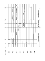
- FIG. 6 is a timing diagram illustrating driving of a pixel unit in the present embodiment. It is a circuit diagram which shows the structure of the pixel part in 2nd Embodiment.
- FIG. 6 is a timing diagram illustrating driving of a pixel unit in the present embodiment. It is a block diagram of the display apparatus in this embodiment. It is a block diagram which shows the display apparatus in 3rd Embodiment.
- FIG. 6 is a timing diagram illustrating driving of a pixel unit in the present embodiment.
- FIG. 1 is a diagram showing a basic configuration of a pixel unit according to a display device of an embodiment of the present invention.
- the pixel unit 1 includes a holding unit 2 and a light emission control unit 4.
- the pixel unit 1 adjusts the light emission amount of the light emitting element provided in the light emission control unit 4 so as to emit light with brightness according to the written input data.
- the pixel unit 1 performs color display, the pixel unit 1 includes a plurality of sub-pixels. In this case, a plurality of sets of the holding unit 2 and the light emission control unit 4 are provided according to the number of sub-pixels in the pixel unit 1.
- the pixel unit 1 includes a data signal line Dj to which input data is supplied, a scanning line SCi (scanning signal line) indicating writing timing (sampling timing), various control signals (signal sTRN, signal sCV, signal sEV, signal sEMI, A set of control lines CLk to which a signal sINI) is supplied and a power supply line (VSS or the like) serving as a reference potential are connected. Details of each signal will be described later.
- the holding unit 2 receives input data indicating the light emission amount of the light emitting element via the data signal line Dj, and is supplied as described above according to the write timing (sampling timing) supplied via the scanning line SCi. Input data is held in a capacitance (indicated by C1 in FIG. 4).
- the light emission control unit 4 includes a drive unit that supplies a drive current for causing the light emitting element to emit light.
- the drive unit includes an active semiconductor element that adjusts the drive current of the light-emitting element, and the light-emission control unit 4 performs compensation processing that compensates the value of the drive current of the light-emitting element according to the threshold characteristic of the active semiconductor element. To do.
- the light emission control unit 4 generates a value of the driving current of the light emitting element compensated by the above compensation processing based on the input data held in the holding unit 2, and controls the driving current according to the generated value.
- the holding unit 2 holds the supplied input data, so that the light emission control unit 4 compensates the value of the drive current that flows through the light emitting element based on the input data held by the holding unit 2.
- the light emission control unit 4 can compensate the value of the drive current that flows through the light emitting element after the holding unit holds the input data.
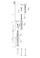
- FIG. 2 is a timing chart showing display control of the pixel portion in the present embodiment.
- FIG. 2 shows the timing of control for displaying the video signals of three frames from the Nth frame to the (N + 2) th frame on the pixel portion.
- Each frame is processed in the following three periods. These three periods are a writing process period, a compensation process period, and a light emission period.
- Write processing period T S is a period for holding the holding portion 2 input data. In the write processing period T S, the input data to be written to the frame as a unit in synchronization with the vertical synchronization period, each of the holding unit 2 holds.
- the write processing period T S which is supplied at the time of a plurality of input data division, the input data of which the target is written into the holding portion 2 corresponding to the input data.
- Compensation processing period T C is the period during which the light emission control unit 4 compensates each value of the drive current of the light emitting element.
- the light emission control unit 4 in this compensation processing period T C is adapted to generate the value of the drive current of the light emitting element based on the input data held in the holding unit 2, to compensate for the value of the generated drive current.
- the light emission period TL is a period in which each light emitting element emits light with brightness according to the value of the compensated drive current.
- the processing performed in units of frames is assigned to any one of the writing processing period T S , the compensation processing period T C , and the light emission period T L whose periods do not overlap each other.
- the processing performed in units of frames is executed in the order of the writing processing period, the compensation processing period, and the light emission period.
- the process is executed in the order of the writing process period T S (N), the compensation process period T C (N), and the light emission period T L (N).
- the processing is executed in the order of the writing processing period T S (N + 1), the compensation processing period T C (N + 1), and the light emission period T L (N + 1).
- the processing is executed in the order of the writing processing period T S (N + 2), the compensation processing period T C (N + 2), and the light emission period T L (N + 2).
- the time allotted for display of each frame is the length of the vertical scanning period (1 V).
- the writing process period T S (N) and the compensation process period T C (N) are allocated to the vertical scanning period (1V) of the Nth frame, but the light emission period T L (N) does not fit in the vertical scanning period (1 V) of the Nth frame. Therefore, the light emission period T L (N) is assigned to the next (N + 1) frame.
- the writing process period T S (N) and the light emission period T L (N) are assigned to two frame periods, respectively.
- the light emission control unit 4 compensates the value of the drive current that flows through the light emitting element in the compensation processing period T C (N) after the holding unit 2 holds the input data in the writing processing period Ts (N). .
- the Nth frame and the (N + 1) th frame the write processing period T S (N + 1) in which the holding unit 2 holds the input data in the (N + 1) th frame, and the light emission control unit 4 in the Nth frame. Overlaps the light emission period T L (N) for driving the light emitting element.
- the timing at which the holding unit 2 performs the writing process and the timing at which the light emission control unit 4 performs the process of causing the light emitting element to emit light overlap More specifically, the information (input data) of the Nth frame image is displayed during the (N + 1) th frame while the light emission control unit 4 drives and displays the light emitting element in the light emission period T L (N). As the processing within the write processing period T S (N + 1), the information (input data) of the (N + 1) th frame image is written into the holding unit 2 paired with the light emission control unit 4.
- the timing shown in FIG. 2 is also applied to a display panel provided with a plurality of pixel portions 1.
- a writing process for holding the input data in the plurality of holding units 2 is performed within the writing process period.
- the plurality of light emission control units 4 drive the light emitting elements.
- a writing process period in which input data is held in a plurality of holding units 2 and a plurality of light emission control units 4 The light emitting element can be provided so as to overlap with a period for driving the light emitting element.
- the writing process period in which the plurality of holding units 2 hold the input data and the period in which the plurality of light emission control units 4 drive the light emitting elements overlap, thereby making the writing process period and the plurality of light emission control units.
- Each time can be ensured as compared with the case where 4 is provided separately from the period for driving the light emitting element.
- the plurality of holding units 2 are provided corresponding to different horizontal scanning lines (horizontal scanning signal lines).
- the writing processing period overlaps the period in which the plurality of light emission control units drive the light emitting elements.
- each process can be performed independently, each time can be used more efficiently than the case where they are provided corresponding to the same horizontal scanning signal line.
- a writing process period in which input data is held in a plurality of holding units 2 included in a predetermined range corresponding to a frame and a compensation processing period in which the plurality of light emission control units 4 compensate the values of the drive currents of the light emitting elements are separated. Can be provided.
- the writing process period in which the input data is held in the plurality of holding units and the compensation processing period in which the plurality of light emission control units each compensate the drive current value can be provided separately.
- the plurality of light emission control units 4 may collectively compensate the respective drive current values. As described above, since the plurality of light emission control units collectively perform the process of compensating the value of each drive current, the process can be completed in a shorter time than when performed independently.
- each compensation process period may be implemented by making each compensation process period mutually correspond.
- the plurality of light emission control units can finish the processing in a shorter time than that performed independently because the respective compensation processing periods coincide with each other.
- the drive circuit 6 of the pixel unit 1 can easily control the light amount of the light emitting element by securing the writing process period and the compensation process period.
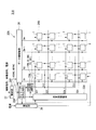
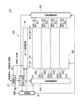
- FIG. 3 is a block diagram showing a configuration of the display device 31A according to the present embodiment.
- the display device 31A includes a display panel 32A, a control unit 37, a timing signal generation unit 38A, and a power supply unit 39.
- the display panel 32A includes a display unit 34A having a plurality of pixel units 1 arranged in a matrix of n rows and m columns, scanning line driving units 33A and 35A for driving each pixel unit 1, and a data line driving unit 36. It is comprised including.
- the display panel 32A is driven by an active scanning type driving method.
- the scanning line driving unit 33A supplies control signals to the control line sets CL2 to CLn.
- the scanning line drive unit 35A supplies control signals to the scanning lines SC1 to SCn.
- the display unit 34A, the scanning line driving units 33A and 35A, and the data line driving unit 36 are monolithically formed on the same substrate in order to reduce the manufacturing process and the wiring capacity. Further, in order to integrate many pixel portions 1 and expand the display area, the display portion 34A, the scanning line driving portions 33A and 35A, and the data line driving portion 36 are polycrystalline silicon thin film transistors formed on a glass substrate, etc. Consists of The above manufacturing process is an example.
- the display unit 34A is partitioned by n scanning lines SC1 to SCn in the horizontal direction and m data signal lines D1 to Dm in the vertical direction that intersect each other, and a plurality of pixel units 1 are located at the intersections of the signal lines. Is provided.
- the sets of control lines CL2 to CLn are provided along the extending direction of the scanning lines SC1 to SCn. Since one control line is provided for every two scanning lines, the total number of control line sets CL2 to CLn is half of the total number of scanning lines SC1 to SCn.
- the control line sets CL2 to CLn include, for example, a control line TRN, a control line CV, a control line EMI, a control line EV, and a control line INI.
- the scanning lines SC1 to SCn send a signal sSCi (control signal) for controlling the holding unit 2 to the pixel unit 1 in a vertical scanning period in which the plurality of pixel units 1 are sequentially scanned.
- a range in which compensation processing for compensating the value of the drive current is collectively performed in a plurality of pixels in a predetermined period determined from the vertical scanning period is defined.
- the set of control lines CL2 to CLn supplies the same control signal to the pixel unit 1 in the range to be collectively implemented. Control signals related to compensation processing and light emission control are supplied by the control line groups CL2 to CLn according to the scanning line group.
- a region where one control line, for example, a set CL2 of control lines is provided is between the two pixel portions 1 to which the scanning lines SC1 and SC2 are respectively connected.
- a wiring region between two corresponding sets of pixel portions 1 wiring from the control line set CL2 to the pixel portion 1 connected to the scanning line SC1 and the scanning line SC2 are connected. Wiring to the pixel portion 1 to be performed can be performed efficiently, and the wiring area can be reduced.
- a wiring region is provided from the control line set CL4 to CLn.
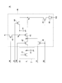
- FIG. 4 is a circuit diagram showing a configuration of the pixel unit 1 in the present embodiment.
- Each active element shown in FIG. 4 is a field effect transistor, particularly a PMOS type, but an NMOS type may also be used.
- the field effect transistor is abbreviated as “transistor” in this embodiment.
- the pixel unit 1A (1) includes a holding unit 2 and a light emission control unit 4A.
- the holding unit 2 includes a transistor 21 and a capacitance C1 (sometimes referred to as “first capacitance”).
- Transistor 21 has a gate connected to scan line SCi and a source connected to data line Dj.
- the capacitance C1 one electrode is connected to the drain of the transistor 21, and the other electrode is connected to the common electrode line.
- the common electrode line is illustrated as ground.
- a connection point between the drain of the transistor 21 and the capacitance C1 is referred to as a node NA.
- the capacitance C1 may be configured by connecting a plurality of capacitors in parallel, or may include stray capacitance in the wiring region.
- the transistor 21 when the scanning line SCi is selected, the transistor 21 is turned on in the holding unit 2, and the voltage applied to the data line Dj is applied to the capacitance C1.
- the capacitance C1 continues to hold the voltage of the capacitance C1 at the time of cutoff. Therefore, to select the scanning line SCi, by applying a video signal DAT to the data signal line Dj, it is possible to hold the voltage for controlling the light intensity of the pixel portion 1 to the node N A.
- the transistor 21 functions as a sampling switch that outputs a voltage corresponding to input data indicating the light emission amount of the pixel at a predetermined timing.
- the holding unit 2 has a simple configuration, it has an effect that the value of the drive current can be compensated based on the voltage held in the capacitance C1 as held input data.
- the light emission control unit 4 ⁇ / b> A includes transistors 41, 42, 43, 44, 45, 46, a capacitance C ⁇ b> 3 (sometimes referred to as “second capacitance”), and a light emitting element 49.
- the transistor 41 has a gate connected to the control line INI and a source connected to the control line VL.
- Transistor 42 has a gate connected to the control line TRN, a source connected to the node N A of the holder 2.
- the transistor 43 has a gate connected to the drain of the transistor 41 and a source connected to the drain of the transistor 42.
- the connection point between the drain and source of the transistor 43 of the transistor 42 and the node N C the connection point between the drain of the gate and the transistor 41 of the transistor 43 is referred to as a node N B.
- the node N B is connected to one electrode of the capacitance C3, the other electrode is connected to the common electrode line.
- Transistor 44 has a gate connected to the control line CV, a source connected to node N B, and a drain connected to the drain of the transistor 43.
- the connection point between the drains of the transistor 44 of the transistor 43 is referred to as a node N D.
- Transistor 46 has a gate connected to the control line EMI, the source is connected to the control line EV, a drain connected to the node N C.
- Transistor 45 has a gate connected to the control line EMI, the drain is connected to node N D, and a source connected to the anode of the light emitting element 49.
- the light emitting element 49 has a cathode connected to the power supply line VSS.
- the transistor 44 When the voltage of the control line CV is applied to the gate of the transistor 44, the transistor 44 is turned off, and when the voltage of the control line INI is applied to the gate of the transistor 41 to make the transistor 41 conductive, the voltage of the control line VL is reduced. Applied to the capacitance C3, the potential of the capacitance C3 is initialized.
- the control unit 37 generates a video signal DAT, a signal VSYNC that is a synchronization signal in the vertical scanning period, a signal HSYNC that is a synchronization signal in the horizontal scanning period, and the like based on the control signal and the video signal supplied from the outside. To do.
- the control unit 37 supplies the video signal DAT to each pixel unit 1 to the data line driving unit 36 in a time division manner.
- the controller 37 supplies the signals VSYNC and HSYNC to the timing signal generator 38A.
- the timing signal generation unit 38A generates various timing signals that cause the display unit 34A, the scanning line driving units 33A and 35A, the data line driving unit 36, and the power supply unit 39 to function.
- the timing signal generation unit 38A supplies the generated timing signal to the scanning line driving unit 33A.
- the timing signal for causing the scanning line driving unit 33A to function is synchronized with the signal VSYNC.
- the timing signal generation unit 38A generates a timing signal that causes the scanning line driving unit 35A and the data line driving unit 36 to function, and supplies the generated timing signal to the scanning line driving unit 35A and the data line driving unit 36.
- Timing signals that cause the scanning line driving unit 35A and the data line driving unit 36 to function are synchronized with the signal VSYNC and the signal HSYNC.
- the timing signal generation unit 38A supplies a timing signal to the power supply unit 39.
- the timing signal for causing the power supply unit 39 to function is synchronized with the signal VSYNC and the signal HSYNC.
- the timing signal generation unit 38A provides a control signal for providing a compensation processing period for performing compensation processing collectively for a plurality of pixels in a predetermined period determined from vertical scanning periods in which the plurality of pixel units 1 are sequentially scanned. Generate.
- This compensation processing is processing for compensating the value of the drive current of the light emitting element 49 in the light emission control unit 4A.
- various timing signals for driving the display device (display panel) are generated, and a predetermined period determined from the vertical scanning period is set as a compensation processing period, and compensation processing for a plurality of pixels is performed at once. Can be implemented.
- the timing signal generation unit 38A generates a control signal in which a writing process period and a compensation process period for holding the drive current in the holding unit 2 are different in the vertical scanning period.
- the timing signal generation unit 38 ⁇ / b> A generates a control signal for controlling the writing process period to be included in the light emission period in which the light emitting element 49 emits light.
- the data line driver 36 extracts video data to be supplied to each pixel unit 1 from the video signal DAT in synchronization with the timing signal supplied from the timing signal generator 38A. Specifically, the data line driving unit 36 extracts the video signal DAT in synchronization with the timing signal supplied from the timing signal generating unit 38A, and outputs the video signal DAT to each of the data signal lines D1 to Dm.
- signals output to the data signal lines D1 to Dm are analog signals corresponding to the video signal DAT. In this case, the data line driving unit 36 generates a voltage corresponding to the video signal DAT based on the video signal DAT.
- the scanning line driving unit 33A outputs, to the scanning lines SC1 to SCn, scanning signals having different timings by a predetermined interval in synchronization with the timing signal supplied from the timing signal generation unit 38A.
- control unit 37 and the power supply unit 39 are supplied with power from the outside.
- the power supply unit 39 supplies power to each unit in the display device and determines a reference potential for causing each unit to function.
- FIG. 5 is a timing chart showing driving of the display unit 34A. Processing related to driving of the display unit 34A includes processing performed in the writing processing period, the threshold compensation processing period, and the light emission period.
- the signal SSCI shows, from the top, other step numbers indicating the stage of processing, the signal SSCI, input data SDJ, the potential of the node N A (V1), the signal Sini, the potential of the node N B (V2), signal SEV,
- the signals sCV, sEMI, and sTRN are shown side by side.
- the input data SDJ, the potential of the node N A (V1), the node N B in potential (V2), the signal sEV indicates an analog value indicating the respective potentials.
- the signal sSCi, the signal sINI, the signal sCV, the signal sEMI, and the signal sTRN take a logic state binarized into an H (high) level and an L (low) level.
- the timing for changing the state of various signals shown in FIG. 5 is generated by the timing signal generator 38A.
- Step 0 The initial state of each signal is determined as follows.
- the signal levels of all control signals that is, signal sSCi, signal sINI, signal sCV, signal sEMI, and signal sTRN are set to the H level. Accordingly, the transistors 21, 41, 42, and 44 to 46 are cut off.
- Transistor 43 take one of two states conducting or blocked depending on the potential of the potential (V2) of the node N B in the previous frame.
- Step 1 The signal sSCi is changed to L level, and the voltage Vdata corresponding to the value of the input data to be written is supplied to the input data Dj. Since the signal sSCi is applied to the gate of the transistor 21, the transistor 21 becomes conductive, the potential of the node N A (V1) becomes Vdata. Therefore, the capacitor C1 is charged to the voltage of Vdata.
- Step 2 The signal sSCi is returned to the H level, and the transistor 21 is changed to the cutoff state.
- the potential of the node N A is held Vdata based on the voltage of the capacitor C1.
- Step 11 The voltage VL is supplied to the source of the transistor 41, and the signal sINI is changed to the L level.
- the transistor 41 the signal sINI is applied to the gate becomes conductive, the potential of the node N B becomes VL.
- Capacitor C3 having one electrode connected to the node N B is in a state that is charged to the voltage VL.
- Step 12 The signal sINI is returned to the H level, and the transistor 41 to which the signal sINI is applied to the gate is changed to the cutoff state.
- the transistor 43 is conductive.
- the signal sEV is set to the voltage Vini
- the signal sCV is transited to the L level
- the signal sEMI is transited from the H level to the L level.
- Transistor 46 which signals sEMI is applied to the gate becomes conductive, the node N C is the potential Vini.
- Vth is a threshold value of the transistor 43.
- the potential Vini and the potential (VL + Vth) satisfy the condition shown in the following formula (1).
- Step 13 While maintaining the signal sCV at the L level, the signal sEMI is returned to the H level, and the signal sTRN is changed to the L level. As a result, the transistor 46 is turned off and the transistor 42 is turned on. Therefore, the potential of the node N B is charged on the basis of the potential of the node N B of the node N A. In short, the potential corresponding to the data input held in the holding unit 2 is transferred to the light emission control unit 4, and compensation processing according to the threshold characteristic of the transistor 43 is performed in generating the value of the drive current.
- Step 14 The signal sCV is returned to the H level, the signal sTRN is returned to the H level, and the transistor 44 and the transistor 42 are turned off. Further, the potential VDD is supplied to the signal sEV, and the signal sEMI is again shifted to the L level. Accordingly, the transistor 46 and the transistor 45 are turned on, and a desired driving current can be supplied to the light emitting element 49 so that the light emitting element 49 can emit light with desired brightness.
- Step 1 is included in the writing process period
- Step 11 to (Step 13) are included in the compensation process period
- (Step 14) is equivalent to the light emission period.
- the writing process is performed on the pixel unit 1 according to a horizontal scanning line different from the horizontal scanning line on which the processing of (Step 1) is performed.
- V2 VL (3)
- V2 Vini-Vth (4)
- Vth is a threshold value of the transistor 43.
- the threshold value information of the transistor 43 is written as the information held by the capacitor C3 through the transistor 42 and the transistor 43, and the condition of the formula (5) is satisfied. .
- the potential V2 in determining the initial value of the potential V2 of the node N B of formula (4), the potential V2 is set further lower than the lower input data Vdata as Vth potential.
- Q1 is a charge accumulated in the capacitance C1
- Q2 is a charge accumulated in the capacitance C3.
- V2 V1-Vth (8)
- V2 C1 / (C1 + C2) ⁇ Vdata + C2 / (C1 + C2) ⁇ Vini ⁇ Vth (12)
- the drive current IL has no term dependent on the threshold value Vth, so that the drive current can be derived without being influenced by the threshold value.
- Threshold value compensation time can be reduced by dividing the write process period and the compensation process period and performing threshold compensation collectively in a certain display area. Further, it is desirable that the display area for performing threshold compensation collectively is the number of scanning lines obtained by dividing the total number of scanning lines (for 1 V) by an integer. For example, after data for 1V is latched in the pixel electrode, threshold compensation is performed collectively. In the threshold compensation, the charge stored in the data latch unit is transferred to the threshold compensation unit, and the threshold compensated voltage of the transistor 43 is generated.
- the display device 31A can easily control the light amount of the light emitting element by securing the writing process period and the compensation process period.
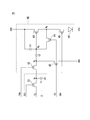
- FIG. 6 is a circuit diagram showing a configuration of the pixel unit 1 in the present embodiment.
- a pixel unit 1B (1) illustrated in FIG. 6 includes a holding unit 2 and a light emission control unit 4B.
- a pixel unit 1B shown in FIG. 6 is different from the pixel unit 1A shown in FIG. 4 in that a light emission control unit 4B is provided instead of the light emission control unit 4A shown in FIG. Further, the signal sINI and the signal sEV are deleted from the control signal from the timing signal generator 38A.
- the light emission control unit 4B includes transistors 42, 43, 44, 45, and 48, capacitances C2 and C3, and a light emitting element 49.
- Transistor 42 has a gate to the control line TRN, a source connected to the node N A of the holder 2.
- the transistor 48 has a gate connected to the control line CV, a source connected to the power supply VDD, and a drain connected to the drain of the transistor 42.
- the connection point between the drains of the transistor 48 of the transistor 42 is referred to as a node N C. To node N C, the one electrode of the capacitance C2 is connected.
- the transistor 44 has a gate connected to the control line CV and a source connected to the other electrode of the capacitance C2.
- the connection point between the other electrode of the source and the capacitance C2 of the transistor 44 is referred to as a node N B.
- the node N B is connected to one electrode of the capacitance C3, the other electrode of the capacitance C3 is connected to the power supply line VDD.
- Transistor 43 has a gate connected to node N B, the source is connected to the power supply line VDD, a drain connected to the drain of the transistor 44.
- the connection point between the drains of the transistor 44 of the transistor 43 is referred to as a node N E.
- Transistor 45 has a gate connected to the control line EMI, the drain is connected to node N E, the source is connected to the anode of the light emitting element 49.
- the light emitting element 49 has a cathode connected to the power supply line VSS.
- FIG. 7 is a timing chart showing driving of the pixel portion in the present embodiment.
- the timing chart shown in FIG. 7 shows the processes corresponding to the above-described writing process period, threshold compensation process period, and light emission period in order of time series.
- step numbers indicating the stages of processing are shown at the top. 7, from the top, the signal SSCI, input data SDJ, the potential of the node N A (V1), the potential of the node N B (V2), the potential of the node N C (V3), the signal SCV, signal SEMI, signal Each signal of sTRN is shown side by side.
- the input data SDJ, the potential of the node N A (V1), the potential of the node N B (V2), the potential of the node N C (V3) indicates the analog value indicating the respective potentials
- the signal sSCi , Signal sCV, signal sEMI, and signal sTRN indicate binarized logic states.
- Step 0 The initial state of each signal is determined as follows.
- the signal levels of all control signals (signal sSCi, signal sCV, signal sEMI, signal sTRN) are set to H (high) level.
- Step 1 The signal sSCi is changed to L (low) level, and the potential Vdata corresponding to the value of the input data to be written is supplied to the input data sDj.
- the potential of the node N A becomes transistor 21 is in a conducting state (V1) is a potential Vdata.
- Step 2 The signal sSCi is returned to the H level, and the transistor 21 is changed to the cutoff state. Thus, the potential of the node N A (V1) is kept at the potential Vdata.
- Step 12 The signal sCV is changed to L level.
- the transistor 48 becomes conductive, the potential of the node N C (V3) is charged to the potential VDD.
- transistor 44 becomes conductive, the potential of the node N B (V2) is a potential (VDD-Tth (threshold of the transistor 43)).
- Step 13 The signal sCV is returned to the H level, and the signal sTRN is changed to the L level. This causes the transistors 44 and 48 cut-off state, the transistor 42 is turned on, the node N A potential (V1) and the node N C potential (V3) and a node N B of potential based on ( V2) is charged.
- a voltage corresponding to the data input held in the holding unit 2 is transferred to the light emission control unit 4B, and a compensation process according to the threshold characteristic of the transistor 43 is performed when generating the value of the drive current.
- Driving current is determined based on the potential (V2) of the node N B.
- Step 14 The signal sTRN is returned to the H level, and the transistor 42 is turned off. Further, the signal sEMI is shifted to the L level. As a result, the TR 48 becomes conductive, and a desired drive current can be supplied to the light emitting element 49 to cause the light emitting element 49 to emit light with a desired brightness.
- Step 1 is included in the writing processing period
- Step 12 and (Step 13) are included in the compensation processing period
- (Step 14) corresponds to the light emission period.
- V2 VDD-Vth (16)
- Vth is the threshold value of the transistor 43.
- the amount of charge accumulated in each of the node NA and the node NC at the time when the signal sCV transitions to H is expressed as Q1 and Q3. Then, the following formula (17) is derived.
- V3 (Vdata ⁇ C1 + VDD ⁇ C2 ⁇ C3 / (C2 + C3)) / (C1 + C2 ⁇ C3 / (C2 + C3)) (19)
- Equation (20) shows the potential V2 in consideration of the influence of the potential change.
- ⁇ represents a coefficient
- Vth is a threshold value of the transistor 43.
- the drive current IL has no term dependent on the threshold value Vth, so that the drive current can be derived without being influenced by the threshold value.
- the display device can secure the writing process period and the compensation process period to facilitate the control of the light amount of the light emitting element.
- FIG. 8 is a block diagram of the display device in the present embodiment.
- a display device 31B shown in FIG. 8 includes a display panel 32B, a control unit 37, a timing signal generation unit 38A, and a power supply unit 39.
- a display device 31B shown in FIG. 8 is different from the display device 31A shown in FIG. 3 of the first embodiment in a display panel 32B.
- the display panel 32B includes a display unit 34B having pixel units 1 arranged in a matrix, scanning line driving units 33B and 35A for driving each pixel unit 1, and a data line driving unit 36.
- a display panel 32B shown in FIG. 8 is different from the display panel 32A shown in FIG. 3 in a display unit 34B and a scanning line driving unit 33B.
- the display unit 34B in the present embodiment is further provided with a set of control lines CL2 to CLm along the extending direction of the data signal lines D1 to Dm.
- the control line set CL since the control line set CL is provided for each of the two data signal lines, the total number of the control line sets CL2 to CLm is half the number (m) of the data signal lines D1 to Dm. It is.
- the control line set CL includes, for example, a control line TRN, a control line CV, a control line EMI, a control line EV, and a control line INI.
- the data signal lines D1 to Dm send input data to be written to the holding unit 2 of the plurality of pixels to the pixel unit 1 in a vertical scanning period in which the plurality of pixels are sequentially scanned.
- a range in which compensation processing for compensating the value of the drive current is collectively performed in a plurality of pixels in a predetermined period determined from the vertical scanning period is defined.
- the set of control lines CL2 to CLn supplies the same control signal to the pixel unit 1 in the range to be collectively implemented. Control signals relating to compensation processing and light emission control are supplied by the control line sets CL2 to CLn according to the set of scanning lines.
- the region where the control line set CL2 is wired is provided between the two pixel portions 1 to which the data signal lines D1 and D2 are respectively connected.
- the wiring from the control line set CL2 to the pixel portion 1 connected to the data signal line D1 and the data signal line D2 are connected.
- Wiring to the pixel portion 1 can be performed efficiently, and the wiring area can be reduced.
- a wiring region is provided from the control line set CL4 to CLm.
- the scanning line is wired with a high resistance metal, but the data signal line is often wired with a low resistance metal.
- the data signal line is often wired with a low resistance metal.
- the scanning line driving unit 33B includes a driver circuit that drives the control line set CL.
- the scanning line driving unit 33B supplies various control signals to the control line sets CL2 to CLm provided along the extending direction of the data signal lines D1 to Dm.
- the display device 31B (display panel 32B) can secure the writing process period and the compensation process period to facilitate the control of the light amount of the light emitting element.
- FIG. 9 is a block diagram showing the display device in the present embodiment.
- a display device 31C illustrated in FIG. 9 includes a display panel 32C, a control unit 37, a timing signal generation unit 38C, and a power supply unit 39.
- a display device 31C shown in FIG. 9 is different from the display device 31A shown in FIG. 3 of the first embodiment in a display panel 32C and a timing signal generator 38C.
- the display panel 32 ⁇ / b> C includes a display unit 34 ⁇ / b> C having the pixel units 1 arranged in a matrix, scanning line driving units 33 ⁇ / b> C and 35 ⁇ / b> C that drive each pixel unit 1, and a data line driving unit 36.
- the display panel 32C shown in FIG. 9 is different from the display panel 32A shown in FIG. 3 in the display unit 34C and the scanning line driving units 33C and 35C.
- a plurality of pixel units 1 are arranged in a matrix, but these pixel units are further divided into a plurality of regions. For example, as shown in FIG. 9, it is divided into four regions (regions 34C1 to C4).
- a control signal related to light emission control and compensation processing for generating a drive current value is independently supplied to each of the divided regions 34C1 to C4.
- a signal sTRN1, a signal sCV1, a signal sEMI1, a signal sEV1, and a signal sINI1 are supplied to the region 34C1 through the scanning line driving unit 33C.
- a signal sTRN2, a signal sCV2, a signal sEMI2, a signal sEV2, and a signal sINI2 are supplied to the region 34C2 via the scanning line driving unit 33C.
- a signal sTRN3, a signal sCV3, a signal sEMI3, a signal sEV3, and a signal sINI3 are supplied to the region 34C3 via the scanning line driving unit 33C.
- a signal sTRN4, a signal sCV4, a signal sEMI4, a signal sEV4, and a signal sINI4 are supplied to the region 34C4 via the scanning line driving unit 33C.
- the signals sTRN1 to sTRN1 to 4 correspond to the signal sTRN described in the first and second embodiments.
- the signals sCV1 to 4 correspond to the signal sCV.
- the signals sEMI1 to sEMI4 correspond to the signal sEMI.
- the signals sEV1 to 4 correspond to the signal sEV.
- Signals sINI1 to sINI4 correspond to the aforementioned signal sINI.
- the scanning line driving unit 33C is synchronized with the timing signal supplied from the timing signal generating unit 38C at a predetermined interval. Scan signals with different timings are output for each region. Signals sSC1 to sSCa are supplied to the region 34C1 through the scanning line driving unit 35C. Signals sSCa + 1 to sSC2a are supplied to the region 34C2 via the scanning line driving unit 35C. Signals sSC2a + 1 to sSC3a are supplied to the region 34C3 via the scanning line driving unit 35C. Signals sSC3a + 1 to sSC4a are supplied to the region 34C4 via the scanning line driving unit 35C.
- the signals sSC1 to sSCa, signals sSCa + 1 to sSC2a, signals sSC2a + 1 to sSC3a, and signals sSC3a + 1 to sSC4a correspond to the signals sSC1 to sSCn described in the first and second embodiments, and the supply destinations are set for each region. The difference is that it is divided. Similarly, scan lines SC1 to SCa, scan lines SCa + 1 to SC2a, scan lines SC2a + 1 to SC3a, and scan lines SC3a + 1 to SC4a are equivalent to scan lines SC1 to SCn, and the supply destination is divided for each region. Different.
- FIG. 10 is a timing chart showing display control of the pixel portion in the present embodiment.
- FIG. 10 shows the timing of control for displaying the video signals of three frames from the (N ⁇ 1) th frame to the (N + 1) th frame on the pixel portion in correspondence with the four areas.
- Each frame is processed in the following three periods.
- the three periods are a writing process period, a compensation process period, and a light emission period, as in FIG.
- the processing performed in units of frames is performed in the order of the writing processing period, the compensation processing period, and the light emission period.
- the processing is performed in the order of the writing processing period T SZ1 (N), the compensation processing period T CZ1 (N), and the light emission period T LZ1 (N).
- the (N + 1) th frame processing is performed in the order of the writing processing period T SZ1 (N + 1), the compensation processing period T CZ1 (N + 1), and the light emission period T LZ1 (N + 1).
- the write processing period T SZ2 (N-1), the compensation processing period T CZ2 (N-1), is processed in the order of the light-emitting period T LZ2 (N-1) .
- the write processing period T SZ2 (N), the compensation processing period T CZ2 (N) is processed in the order of the light-emitting period T LZ2 (N).
- the processing is performed in the order of the write processing period T SZ3 (N ⁇ 1), the compensation processing period T CZ3 (N ⁇ 1), and the light emission period T LZ3 (N ⁇ 1). .
- the processing is performed in the order of the write processing period T SZ3 (N), the compensation processing period T CZ3 (N), and the light emission period T LZ3 (N).
- the processing is performed in the order of the write processing period T SZ4 (N ⁇ 1), the compensation processing period T CZ4 (N ⁇ 1), and the light emission period T LZ4 (N ⁇ 1).
- processing is performed in the order of the writing processing period T SZ4 (N), the compensation processing period T CZ4 (N), and the light emission period T LZ4 (N).
- the write processing period of the Nth frame attention is focused on the write processing period of the Nth frame.
- the write process period T SZ1 (N) in the area 34C1 the write process period T SZ2 (N) in the area 34C2
- the write process period T SZ3 in the area 34C3 ( N) and the write processing period T SZ4 (N) in the region 34C4. Since the area is divided into four equal parts, the length of each writing process period is (1/4) V of the vertical scanning period. In short, the sum of the lengths of the four write processing periods is the vertical scanning period (1 V).
- each of the divided areas 34C1 to 34C4 is independently supplied with a control signal related to compensation processing for generating a drive current value and light emission control. Control is possible.
- the time for holding unit 2 to hold the input data is reduced. It is possible to suppress the influence of the leakage current to thereby voltage held in the holding section 2 (voltage of the node N A (V1)).
- the display device (display panel, drive circuit) shown in each of the above embodiments can easily control the light amount of the light emitting element.
Landscapes
- Engineering & Computer Science (AREA)
- Physics & Mathematics (AREA)
- Computer Hardware Design (AREA)
- General Physics & Mathematics (AREA)
- Theoretical Computer Science (AREA)
- Control Of Indicators Other Than Cathode Ray Tubes (AREA)
- Control Of El Displays (AREA)
Abstract
表示装置の各画素部(1)において、入力データを保持する保持部(2)と、前記保持部(2)が保持した入力データに基づいて発光素子(49)に流す駆動電流の値を補償する発光制御部(4)とを設け、前記発光制御部(4)がNフレーム目の画像の入力データを発光期間TL(N)において前記発光素子(49)を駆動して表示させている間に、(N+1)フレーム目の書込み処理期間TS(N+1)内の処理として、(N+1)フレーム目の画像の入力データを、前記発光制御部(4)と対になる前記保持部(2)に書き込む。
Description
本発明は、表示装置の駆動回路、表示装置および駆動方法に関する。
本願は、2012年12月19日に、日本に出願された特願2012-277113号に基づき優先権を主張し、その内容をここに援用する。
本願は、2012年12月19日に、日本に出願された特願2012-277113号に基づき優先権を主張し、その内容をここに援用する。
表示装置(表示パネル)の駆動方式として、多画素化および高精細化に適したアクティブ走査型の駆動方式が利用されている。このような表示装置において、多画素化および高精細化による画素数の増加に伴って、単位時間当たりに表示装置に書き込まれるデータ数が増加する傾向にある。
また、表示装置の一種に有機EL(エレクトロルミネッセンス)ディスプレイがある。
有機ELディスプレイは、個々の画素に設けられた発光素子の発光量を調節することにより画像を形成して表示する。ただし、発光素子を駆動する駆動回路の特性(閾値特性)が変化すると、表示する画像の画質が低下する。このような画質の低下を低減させるため、駆動回路の特性に応じて画素ごとに発光素子の駆動電流を補正して、画質の低下を低減させる技術が知られている(特許文献1)。
特許文献1によれば、表示するデータ(入力データ)の書込み処理期間と発光期間を各走査線の水平走査期間に対応させて設けており、書込み処理期間において書き込んだデータに基づいて、発光期間の発光量(画素の明るさ)を制御している。画質の低下を低減させるための駆動回路の特性(閾値特性)に応じた補償は、書込み処理期間において行っている。
また、表示装置の一種に有機EL(エレクトロルミネッセンス)ディスプレイがある。
有機ELディスプレイは、個々の画素に設けられた発光素子の発光量を調節することにより画像を形成して表示する。ただし、発光素子を駆動する駆動回路の特性(閾値特性)が変化すると、表示する画像の画質が低下する。このような画質の低下を低減させるため、駆動回路の特性に応じて画素ごとに発光素子の駆動電流を補正して、画質の低下を低減させる技術が知られている(特許文献1)。
特許文献1によれば、表示するデータ(入力データ)の書込み処理期間と発光期間を各走査線の水平走査期間に対応させて設けており、書込み処理期間において書き込んだデータに基づいて、発光期間の発光量(画素の明るさ)を制御している。画質の低下を低減させるための駆動回路の特性(閾値特性)に応じた補償は、書込み処理期間において行っている。
しかしながら、特許文献1に示される技術によれば、書込み処理期間と補償処理期間(閾値補償期間)が水平走査期間にそれぞれ必要であるため、表示装置の高精細化が進むと、書込み処理期間および補償処理期間を十分に確保できず、発光素子の光量を制御できなくなるという問題があった。
本発明は、上記問題を解決すべくなされたもので、その目的は、表示装置の光量の制御を容易にする表示装置の駆動回路、表示装置および駆動方法を提供することにある。
[1]この発明は上述した課題を解決するためになされたものであり、本発明の一態様は、供給された入力データを保持する保持部と、前記保持部が保持した入力データに基づいて発光素子に流す駆動電流の値を補償する発光制御部とを備えることを特徴とする駆動回路である。
[2]また、上記駆動回路の一態様は、前記発光制御部は、前記保持部が前記入力データを保持した後に、前記発光素子に流す駆動電流の値を補償することを特徴とする。
[3]また、上記駆動回路の一態様は、前記保持部に入力データを保持させる書込み処理期間と、前記発光制御部が前記発光素子を駆動する期間とが重複することを特徴とする。
[4]また、上記駆動回路の一態様は、複数の前記保持部において前記入力データを保持させる書込み処理期間と、複数の前記発光制御部が前記駆動電流の値をそれぞれ補償する補償処理期間とを分離して設けていることを特徴とする。
[5]また、上記駆動回路の一態様は、前記複数の発光制御部は、それぞれの前記駆動電流の値を補償する処理を一括して実施することを特徴とする。
[6]また、上記駆動回路の一態様は、前記複数の発光制御部は、それぞれの前記補償処理期間を互いに一致させていることを特徴とする。
[7]また、上記駆動回路の一態様は、複数の前記保持部に前記入力データを保持させる書込み処理期間と、前記複数の前記発光制御部が前記発光素子を駆動する期間とが重複することを特徴とする。
[8]また、上記駆動回路の一態様は、前記複数の保持部は、異なる水平走査信号線に対応して設けられていることを特徴とする。
[9]また、上記駆動回路の一態様は、前記保持部は、前記発光素子の発光量を示す入力データに応じた電圧を、定められた所定のタイミングに出力するサンプリングスイッチと、前記サンプリングスイッチから出力される電圧を保持する第1の静電容量とを備え、前記発光制御部は、前記保持された入力データとして、前記第1の静電容量に保持された電圧に基づいて前記駆動電流の値を補償することを特徴とする。
[10]また、本発明の一態様は、複数の画素がマトリクス状に配列されるアクティブ走査型の表示装置であって、上記の保持部と発光制御部とを対にしてそれぞれ備えており、前記発光制御部が調整する画素の明るさを示す入力データが書き込み処理によって前記保持部に書き込まれることを特徴とする表示装置である。
[11]また、上記表示装置の一態様は、前記複数の画素を順に走査する垂直走査期間において、前記複数の画素を順に走査して前記保持部を制御する制御信号を前記画素に送る走査信号線と、前記垂直走査期間のうちから定められた所定の期間に、前記発光制御部において前記駆動電流の値を補償する補償処理を前記複数の画素において一括して実施する範囲に含まれる前記画素に対して、前記走査信号線の延伸方向に沿って、2つの前記走査信号線を組にして前記走査信号線の組ごとに前記補償処理および発光制御にかかわる制御信号を送る制御線とを備え、前記補償処理および発光制御にかかわる制御信号が前記走査信号線の組に応じた信号が供給されることを特徴とする。
[12]また、上記表示装置の一態様は、前記複数の画素を順に走査する垂直走査期間において、前記複数の画素の前記保持部に書き込む入力データを前記画素に送るデータ信号線と、前記垂直走査期間のうちから定められた所定の期間に、前記発光制御部において前記駆動電流の値を補償する補償処理を前記複数の画素において一括して実施する範囲に含まれる前記画素に対して、前記データ信号線の延伸方向に沿って、2つの前記データ信号線を組にして前記データ信号線の組ごとに前記補償処理および発光制御にかかわる制御信号を送る制御線とを備え、前記補償処理および発光制御にかかわる制御信号が前記データ信号線の組に応じた信号が供給されることを特徴とする。
[13]また、上記表示装置の一態様は、前記複数の画素が設けられた表示部の領域が複数の領域に分割され、前記分割された領域のそれぞれに対して、前記駆動電流の値を生成させる補償処理および発光制御にかかわる制御信号が独立して供給されることを特徴とする。
[14]また、上記表示装置の一態様は、前記複数の画素を順に走査する垂直走査期間のうちから定められた所定の期間に、前記発光制御部において前記駆動電流の値を生成させる補償処理を前記複数の画素において一括して実施する補償処理期間を設けた制御信号が供給され、前記発光制御部は、前記発光素子を駆動する駆動部を備え、前記発光制御部は、前記補償処理期間を設けた制御信号に応じて、前記補償処理期間に前記駆動部の閾値特性に応じて前記駆動電流の値を補償することを特徴とする。
[15]また、上記表示装置の一態様は、前記複数の画素を順に走査する垂直走査期間のうち、前記供給された入力データを前記保持部において保持させる書込み処理期間と前記駆動電流の値をそれぞれ補償する補償処理期間とを異なる期間に設けた制御信号が供給され、前記保持部は、前記書込み処理期間と前記補償処理期間とを異なる期間に設けた制御信号に応じて、前記書込み処理期間に前記供給された入力データを保持することを特徴とする。
[16]また、上記表示装置の一態様は、前記書込み処理期間が、前記発光素子を発光させる発光期間に含まれている制御信号が供給され、前記発光制御部は、前記書込み処理期間が、前記発光素子を発光させる発光期間に含まれている制御信号に応じて前記発光期間に前記発光素子を発光させることを特徴とする。
[17]また、上記表示装置の一態様は、第1フレームの画像を形成する前記入力データに基づいて前記発光素子を発光させる発光期間において、前記保持部は、前記第1フレームの次の第2フレームの画像を形成する前記入力データを保持することを特徴とする。
[18]また、上記表示装置の一態様は、前記発光制御部は、前記駆動電流を調整する電界効果型トランジスタと、前記電界効果型トランジスタのゲート端子に接続されている第2の静電容量とを備え、前記発光制御部は、前記書込み処理期間と前記補償処理期間との間に、前記電界効果型トランジスタのゲート端子に接続されている第2の静電容量に蓄えられている電荷を放電させることを特徴とする。
[19]また、上記表示装置の一態様は、前記複数の画素を順に走査する垂直走査期間のうちから定められた所定の期間に、前記発光制御部において前記駆動電流の値を生成させる補償処理を前記複数の画素において一括して実施する補償処理期間を設ける制御信号を生成するタイミング信号生成部を備えることを特徴とする。
[20]また、上記表示装置の一態様は、前記タイミング信号生成部は、前記垂直走査期間のうち、前記供給された入力データを前記保持部において保持させる書込み処理期間と前記補償処理期間とを異なる期間に設けた制御信号を生成することを特徴とする。
[21]また、上記表示装置の一態様は、前記タイミング信号生成部は、前記書込み処理期間が、前記発光素子を発光させる発光期間に含まれるように制御する制御信号を生成することを特徴とする。
[22]また、本発明の一態様は、供給された入力データを保持部が保持するステップと、前記保持部が保持した入力データに基づいて発光素子に流す駆動電流の値を補償するステップとを備えることを特徴とする駆動方法である。
本発明によれば、発光素子の光量の制御を容易とする表示装置の駆動回路、表示装置および駆動方法を提供することが可能となる。
以下、図面を参照して、本発明の実施形態について説明する。
(第1実施形態)
図1は、本発明の実施形態の表示装置に係る画素部の基本構成を示す図である。
図1において、画素部1は、保持部2と発光制御部4とを含んで構成される。画素部1は、書き込まれた入力データに応じた明るさで発光するように、発光制御部4に設けられた発光素子の発光量を調整する。
なお、画素部1がカラー表示を行う場合には、画素部1は複数のサブ画素を備える。この場合には、上記の保持部2と発光制御部4との組は、画素部1内のサブ画素の数に応じて複数設けられる。
図1は、本発明の実施形態の表示装置に係る画素部の基本構成を示す図である。
図1において、画素部1は、保持部2と発光制御部4とを含んで構成される。画素部1は、書き込まれた入力データに応じた明るさで発光するように、発光制御部4に設けられた発光素子の発光量を調整する。
なお、画素部1がカラー表示を行う場合には、画素部1は複数のサブ画素を備える。この場合には、上記の保持部2と発光制御部4との組は、画素部1内のサブ画素の数に応じて複数設けられる。
画素部1には、入力データが供給されるデータ信号線Dj、書き込みタイミング(サンプリングタイミング)を示す走査線SCi(走査信号線)、各種制御信号(信号sTRN、信号sCV、信号sEV、信号sEMI、信号sINI)が供給される制御線の組CLk、および、基準電位となる電源線(VSS等)が接続されている。それぞれの信号についての詳細は後述する。
保持部2は、データ信号線Djを介して発光素子の発光量を示す入力データの供給を受け、走査線SCiを介して供給される書き込みタイミング(サンプリングタイミング)に応じて、上述の供給された入力データを静電容量(図4においてC1で示すもの。)に保持する。
発光制御部4は、発光素子を発光させる駆動電流を流す駆動部を備える。駆動部は発光素子の駆動電流を調整する能動型半導体素子を備えており、発光制御部4は、能動型半導体素子の閾値特性に応じて発光素子の駆動電流の値を補償する補償処理を実施する。発光制御部4は、保持部2に保持された入力データに基づいて上記の補償処理によって補償した発光素子の駆動電流の値を生成し、生成した値に応じて駆動電流を制御する。
これにより、供給された入力データを保持部2が保持することにより、発光制御部4は、保持部2が保持した入力データに基づいて、発光素子に流す駆動電流の値を補償する。
また、発光制御部4は、保持部が入力データを保持した後に、発光素子に流す駆動電流の値を補償することもできる。
発光制御部4は、発光素子を発光させる駆動電流を流す駆動部を備える。駆動部は発光素子の駆動電流を調整する能動型半導体素子を備えており、発光制御部4は、能動型半導体素子の閾値特性に応じて発光素子の駆動電流の値を補償する補償処理を実施する。発光制御部4は、保持部2に保持された入力データに基づいて上記の補償処理によって補償した発光素子の駆動電流の値を生成し、生成した値に応じて駆動電流を制御する。
これにより、供給された入力データを保持部2が保持することにより、発光制御部4は、保持部2が保持した入力データに基づいて、発光素子に流す駆動電流の値を補償する。
また、発光制御部4は、保持部が入力データを保持した後に、発光素子に流す駆動電流の値を補償することもできる。
図2は、本実施形態における画素部の表示制御を示すタイミング図である。
図2には、Nフレーム目から(N+2)フレーム目までの3つのフレームの映像信号を画素部に表示させる制御のタイミングを示す。
各フレームの処理を次に示す3つの期間に分けて実施する。この3つの期間は、書込み処理期間、補償処理期間および発光期間である。
書込み処理期間TSは、入力データを保持部2に保持させる期間である。この書込み処理期間TSにおいて、垂直同期期間に同期してフレームを単位として書き込まれる入力データを、それぞれの保持部2が保持する。書込み処理期間TSには、複数の入力データが時分割で供給されており、そのうち対象となる入力データが、当該入力データに対応する保持部2に書き込まれる。
図2には、Nフレーム目から(N+2)フレーム目までの3つのフレームの映像信号を画素部に表示させる制御のタイミングを示す。
各フレームの処理を次に示す3つの期間に分けて実施する。この3つの期間は、書込み処理期間、補償処理期間および発光期間である。
書込み処理期間TSは、入力データを保持部2に保持させる期間である。この書込み処理期間TSにおいて、垂直同期期間に同期してフレームを単位として書き込まれる入力データを、それぞれの保持部2が保持する。書込み処理期間TSには、複数の入力データが時分割で供給されており、そのうち対象となる入力データが、当該入力データに対応する保持部2に書き込まれる。
補償処理期間TCは、発光制御部4が発光素子の駆動電流の値をそれぞれ補償する期間である。例えば、この補償処理期間TCにおいて発光制御部4は、保持部2において保持されている入力データに基づいて発光素子の駆動電流の値を生成するとともに、生成した駆動電流の値を補償する。
発光期間TLは、補償された駆動電流の値に応じた明るさで、発光素子をそれぞれ発光させる期間である。
このように、本実施形態では、フレーム単位で実施する処理を、互いに期間が重複しない書込み処理期間TS、補償処理期間TC、発光期間TLの何れかに割り当てている。
発光期間TLは、補償された駆動電流の値に応じた明るさで、発光素子をそれぞれ発光させる期間である。
このように、本実施形態では、フレーム単位で実施する処理を、互いに期間が重複しない書込み処理期間TS、補償処理期間TC、発光期間TLの何れかに割り当てている。
また、上記のフレーム単位で実施する処理(すなわち、フレームを跨らないで行われる処理)は、書込み処理期間、補償処理期間、発光期間の順に実行される。例えば、Nフレーム目の場合、書込み処理期間TS(N)、補償処理期間TC(N)、発光期間TL(N)の順に従って実行される。同様に、(N+1)フレーム目の場合、書込み処理期間TS(N+1)、補償処理期間TC(N+1)、発光期間TL(N+1)の順に従って処理が実行される。(N+2)フレーム目の場合、書込み処理期間TS(N+2)、補償処理期間TC(N+2)、発光期間TL(N+2)の順に従って処理が実行される。
なお、各フレームの表示に割り当てられる時間は、垂直走査期間(1V)の長さである。図2に示されるように、Nフレーム目の垂直走査期間(1V)には、上記の書込み処理期間TS(N)、補償処理期間TC(N)を割り当てられているが、発光期間TL(N)はNフレーム目の垂直走査期間(1V)に収まらない。そこで、発光期間TL(N)は、次の(N+1)フレーム目に割り当てる。要するに、書込み処理期間TS(N)と発光期間TL(N)とは、2つのフレームの期間にそれぞれ割り当てられている。
上記のように、発光制御部4は、保持部2が書込み処理期間Ts(N)において入力データを保持した後に、補償処理期間TC(N)において発光素子に流す駆動電流の値を補償する。
異なるフレーム、例えば、Nフレーム目と(N+1)フレーム目とにおいて、(N+1)フレーム目において保持部2に入力データを保持させる書込み処理期間TS(N+1)と、Nフレーム目において発光制御部4が発光素子を駆動する発光期間TL(N)とを重複させている。
異なるフレーム、例えば、Nフレーム目と(N+1)フレーム目とにおいて、(N+1)フレーム目において保持部2に入力データを保持させる書込み処理期間TS(N+1)と、Nフレーム目において発光制御部4が発光素子を駆動する発光期間TL(N)とを重複させている。
単一の画素部1に着目し、書込み処理期間と補償処理期間との関係を説明する。同じ画素部1において保持部2が書き込み処理を実施するタイミングと、発光制御部4が発光素子を発光させる処理を実施するタイミングとが重なるタイミングがある。より具体的に説明すると、Nフレーム目の画像の情報(入力データ)を発光期間TL(N)において発光制御部4が発光素子を駆動して表示させている間に、(N+1)フレーム目の書込み処理期間TS(N+1)内の処理として、(N+1)フレーム目の画像の情報(入力データ)が、上記発光制御部4と対になる保持部2に書き込まれる。
次に、複数の画素部1を備える場合において、書込み処理期間と補償処理期間との関係を説明する。この図2に示されるタイミングは、複数の画素部1が設けられた表示パネルの場合にも適用される。この場合、複数の保持部2に入力データをそれぞれ保持させる書き込み処理が書込み処理期間の内で行われる。また、発光期間において、複数の発光制御部4が発光素子をそれぞれ駆動する。そのため、複数の画素部1が設けられている場合においても単一の画素として説明した場合と同様に、複数の保持部2に入力データを保持させる書込み処理期間と、複数の発光制御部4が発光素子を駆動する期間とが重複するように設けることができる。
このように、複数の保持部2に入力データを保持させる書込み処理期間と、複数の発光制御部4が発光素子を駆動する期間とを重複させることにより、書込み処理期間と、複数の発光制御部4が発光素子を駆動する期間とを分けて設けた場合より、それぞれの時間を確保することができる。
このように、複数の保持部2に入力データを保持させる書込み処理期間と、複数の発光制御部4が発光素子を駆動する期間とを重複させることにより、書込み処理期間と、複数の発光制御部4が発光素子を駆動する期間とを分けて設けた場合より、それぞれの時間を確保することができる。
なお、この場合の複数の保持部2は、異なる水平走査線(水平走査信号線)に対応して設けられているものとする。
このように、複数の保持部は、異なる水平走査線に対応して設けられていることにより、書込み処理期間と、複数の発光制御部が発光素子を駆動する期間とを重複させた場合であっても、それぞれの処理を独立に実施することができることから、同じ水平走査信号線に対応して設けた場合より、それぞれの時間を効率良く利用することができる。
このように、複数の保持部は、異なる水平走査線に対応して設けられていることにより、書込み処理期間と、複数の発光制御部が発光素子を駆動する期間とを重複させた場合であっても、それぞれの処理を独立に実施することができることから、同じ水平走査信号線に対応して設けた場合より、それぞれの時間を効率良く利用することができる。
次に、フレーム内の処理に着目し、書込み処理期間と補償処理期間との関係を説明する。フレームに応じた所定の範囲に含まれる複数の保持部2において入力データを保持させる書込み処理期間と、複数の発光制御部4が発光素子の駆動電流の値をそれぞれ補償する補償処理期間とを分離して設けることができる。
このように、複数の保持部において入力データを保持させる書込み処理期間と、複数の発光制御部が駆動電流の値をそれぞれ補償する補償処理期間とを分離して設けることができる。
このように、複数の保持部において入力データを保持させる書込み処理期間と、複数の発光制御部が駆動電流の値をそれぞれ補償する補償処理期間とを分離して設けることができる。
なお、同一フレーム内の閾値補償処理として、複数の発光制御部4は、それぞれの駆動電流の値を一括して補償してもよい。
このように、複数の発光制御部は、それぞれの駆動電流の値を補償する処理を一括して実施することから、独立に実施するより短時間に処理を終えることができる。
このように、複数の発光制御部は、それぞれの駆動電流の値を補償する処理を一括して実施することから、独立に実施するより短時間に処理を終えることができる。
また、複数の発光制御部は、それぞれの補償処理期間を互いに一致させることにより実施してもよい。
このように、複数の発光制御部は、それぞれの補償処理期間を互いに一致させていることから、独立に実施するより短時間に処理を終えることができる。
このように、複数の発光制御部は、それぞれの補償処理期間を互いに一致させていることから、独立に実施するより短時間に処理を終えることができる。
以上に示す本実施形態において、画素部1の駆動回路6は、書込み処理期間および補償処理期間を確保して、発光素子の光量の制御を容易とすることができる。
図3は、本実施形態に係る表示装置31Aの構成を示すブロック図である。表示装置31Aは、表示パネル32A、制御部37、タイミング信号生成部38Aおよび電源部39を備える。
表示パネル32Aは、n行m列のマトリクス状に配列された複数の画素部1を有する表示部34Aと、各画素部1を駆動する走査線駆動部33A、35Aと、データ線駆動部36とを含んで構成される。表示パネル32Aは、アクティブ走査型の駆動方式により駆動される。
走査線駆動部33Aは、制御線の組CL2~CLnに制御信号を供給する。走査線駆動部35Aは、走査線SC1~SCnに制御信号を供給する。
表示パネル32Aは、n行m列のマトリクス状に配列された複数の画素部1を有する表示部34Aと、各画素部1を駆動する走査線駆動部33A、35Aと、データ線駆動部36とを含んで構成される。表示パネル32Aは、アクティブ走査型の駆動方式により駆動される。
走査線駆動部33Aは、制御線の組CL2~CLnに制御信号を供給する。走査線駆動部35Aは、走査線SC1~SCnに制御信号を供給する。
表示部34A、走査線駆動部33A、35Aおよびデータ線駆動部36は、製造時の工程と配線容量を低減するために、同一基板上にモノリシックに形成される。また、多くの画素部1を集積し、表示面積を拡大するために、表示部34A、走査線駆動部33A、35Aおよびデータ線駆動部36は、ガラス基板上に形成された多結晶シリコン薄膜トランジスタなどから構成される。以上の製造時の工程は例示である。
表示部34Aは、相互に交差する水平方向のn本の走査線SC1~SCnおよび垂直方向のm本のデータ信号線D1~Dmによって区画され、各信号線の交点の位置に複数の画素部1が設けられている。
制御線の組CL2~CLnは、走査線SC1~SCnの延伸方向に沿って設けられている。2つの走査線ごとに1つの制御線が設けられることから、制御線の組CL2~CLnの総数は、走査線SC1~SCnの総数の半分である。制御線の組CL2~CLnには、例えば、制御線TRN,制御線CV,制御線EMI,制御線EV,制御線INIが含まれる。
走査線SC1~SCnは、複数の画素部1を順に走査する垂直走査期間において、保持部2を制御する信号sSCi(制御信号)を画素部1に送る。垂直走査期間のうちから定められた所定の期間に、駆動電流の値を補償する補償処理を複数の画素において一括して実施する範囲が定められている。制御線の組CL2~CLnは、一括して実施する範囲の画素部1に対して同じ制御信号を供給する。
制御線の組CL2~CLnにより、補償処理および発光制御にかかわる制御信号が走査線の組に応じた信号が供給される。
1つの制御線、例えば制御線の組CL2を設ける領域は、走査線SC1とSC2がそれぞれ接続される2つの画素部1の間とする。このように、対応する2つの画素部1の組の間に配線領域を設けることにより、制御線の組CL2から、走査線SC1に接続される画素部1までの配線と、走査線SC2に接続される画素部1までの配線を効率よく実施することができ、配線領域を低減することができる。制御線の組CL4からCLnまで同様に配線領域を設けることとする。
このように2つの走査線ごとに補償処理および発光制御にかかわる制御信号を送る制御線を設けたことにより、配線領域を削減することができる。
制御線の組CL2~CLnは、走査線SC1~SCnの延伸方向に沿って設けられている。2つの走査線ごとに1つの制御線が設けられることから、制御線の組CL2~CLnの総数は、走査線SC1~SCnの総数の半分である。制御線の組CL2~CLnには、例えば、制御線TRN,制御線CV,制御線EMI,制御線EV,制御線INIが含まれる。
走査線SC1~SCnは、複数の画素部1を順に走査する垂直走査期間において、保持部2を制御する信号sSCi(制御信号)を画素部1に送る。垂直走査期間のうちから定められた所定の期間に、駆動電流の値を補償する補償処理を複数の画素において一括して実施する範囲が定められている。制御線の組CL2~CLnは、一括して実施する範囲の画素部1に対して同じ制御信号を供給する。
制御線の組CL2~CLnにより、補償処理および発光制御にかかわる制御信号が走査線の組に応じた信号が供給される。
1つの制御線、例えば制御線の組CL2を設ける領域は、走査線SC1とSC2がそれぞれ接続される2つの画素部1の間とする。このように、対応する2つの画素部1の組の間に配線領域を設けることにより、制御線の組CL2から、走査線SC1に接続される画素部1までの配線と、走査線SC2に接続される画素部1までの配線を効率よく実施することができ、配線領域を低減することができる。制御線の組CL4からCLnまで同様に配線領域を設けることとする。
このように2つの走査線ごとに補償処理および発光制御にかかわる制御信号を送る制御線を設けたことにより、配線領域を削減することができる。
図4は、本実施形態における画素部1の構成を示す回路図である。図4に示す各アクティブ素子は、電界効果型トランジスタ、特にPMOS型であるが、NMOS型を用いてもよい。以下では、本実施例に関して電界効果型トランジスタを「トランジスタ」と略称する。
画素部1A(1)は、保持部2と発光制御部4Aとを含んで構成される。なお、画素部1が3原色に応じた複数のサブ画素を含んで構成される場合には、保持部2と発光制御部4Aは、サブ画素の数に応じて複数設けられる。
保持部2は、トランジスタ21と、静電容量C1(「第1の静電容量」と言うことがある)と、を含んで構成される。
トランジスタ21は、ゲートが走査線SCiへ接続され、ソースがデータ線Djに接続される。
静電容量C1は、トランジスタ21のドレインに一方の電極が接続され、他方の電極は、共通電極線に接続されている。図4では、共通電極線を接地として図示する。トランジスタ21のドレインと静電容量C1との接続点をノードNAと称する。
なお、静電容量C1は、複数のコンデンサを並列に接続して構成してもよいし、配線領域の浮遊容量を含めてもよい。
保持部2は、トランジスタ21と、静電容量C1(「第1の静電容量」と言うことがある)と、を含んで構成される。
トランジスタ21は、ゲートが走査線SCiへ接続され、ソースがデータ線Djに接続される。
静電容量C1は、トランジスタ21のドレインに一方の電極が接続され、他方の電極は、共通電極線に接続されている。図4では、共通電極線を接地として図示する。トランジスタ21のドレインと静電容量C1との接続点をノードNAと称する。
なお、静電容量C1は、複数のコンデンサを並列に接続して構成してもよいし、配線領域の浮遊容量を含めてもよい。
したがって、走査線SCiが選択されると、保持部2においてトランジスタ21が導通し、データ線Djに印加された電圧が静電容量C1に印加される。一方、走査線SCiの選択期間が終了して、電界効果トランジスタ21が遮断されている間、静電容量C1は、遮断時の静電容量C1の電圧を保持し続ける。したがって、走査線SCiを選択し、データ信号線Djへ映像信号DATを印加することで、画素部1の光量を制御する電圧をノードNAに保持させることができる。
トランジスタ21は、画素の発光量を示す入力データに応じた電圧を、定められた所定のタイミングで出力するサンプリングスイッチとして機能する。なお、トランジスタ21をサンプリングスイッチとして例示したが、他の形態のスイッチを用いてもよい。
このように、保持部2は簡素な構成でありながら、保持された入力データとして静電容量C1に保持された電圧に基づいて、駆動電流の値を補償することができるという効果を奏する。
トランジスタ21は、画素の発光量を示す入力データに応じた電圧を、定められた所定のタイミングで出力するサンプリングスイッチとして機能する。なお、トランジスタ21をサンプリングスイッチとして例示したが、他の形態のスイッチを用いてもよい。
このように、保持部2は簡素な構成でありながら、保持された入力データとして静電容量C1に保持された電圧に基づいて、駆動電流の値を補償することができるという効果を奏する。
次に、発光制御部4Aについて説明する。
発光制御部4Aは、トランジスタ41、42、43、44、45、46、静電容量C3(「第2の静電容量」と言うことがある。)、および発光素子49を含んで構成される。
トランジスタ41は、ゲートが制御線INIへ接続され、ソースが制御線VLに接続される。
トランジスタ42は、ゲートが制御線TRNへ接続され、ソースが保持部2のノードNAに接続される。
トランジスタ43は、ゲートがトランジスタ41のドレインへ接続され、ソースがトランジスタ42のドレインへ接続される。トランジスタ42のドレインとトランジスタ43のソースとの接続点をノードNCと称し、トランジスタ43のゲートとトランジスタ41のドレインとの接続点をノードNBと称する。
ノードNBには、静電容量C3の一方の電極が接続され、他方の電極は、共通電極線に接続される。
トランジスタ44は、ゲートが制御線CVへ接続され、ソースがノードNBへ接続され、ドレインがトランジスタ43のドレインへ接続される。トランジスタ43のドレインとトランジスタ44のドレインとの接続点をノードNDと称する。
トランジスタ46は、ゲートが制御線EMIへ接続され、ソースが制御線EVへ接続され、ドレインがノードNCへ接続される。
トランジスタ45は、ゲートが制御線EMIへ接続され、ドレインがノードNDへ接続され、ソースが発光素子49のアノードへ接続される。
発光素子49は、カソードが電源線VSSへ接続される。
発光制御部4Aは、トランジスタ41、42、43、44、45、46、静電容量C3(「第2の静電容量」と言うことがある。)、および発光素子49を含んで構成される。
トランジスタ41は、ゲートが制御線INIへ接続され、ソースが制御線VLに接続される。
トランジスタ42は、ゲートが制御線TRNへ接続され、ソースが保持部2のノードNAに接続される。
トランジスタ43は、ゲートがトランジスタ41のドレインへ接続され、ソースがトランジスタ42のドレインへ接続される。トランジスタ42のドレインとトランジスタ43のソースとの接続点をノードNCと称し、トランジスタ43のゲートとトランジスタ41のドレインとの接続点をノードNBと称する。
ノードNBには、静電容量C3の一方の電極が接続され、他方の電極は、共通電極線に接続される。
トランジスタ44は、ゲートが制御線CVへ接続され、ソースがノードNBへ接続され、ドレインがトランジスタ43のドレインへ接続される。トランジスタ43のドレインとトランジスタ44のドレインとの接続点をノードNDと称する。
トランジスタ46は、ゲートが制御線EMIへ接続され、ソースが制御線EVへ接続され、ドレインがノードNCへ接続される。
トランジスタ45は、ゲートが制御線EMIへ接続され、ドレインがノードNDへ接続され、ソースが発光素子49のアノードへ接続される。
発光素子49は、カソードが電源線VSSへ接続される。
制御線CVの電圧がトランジスタ44のゲートに加わることによりトランジスタ44を遮断状態にし、そして制御線INIの電圧がトランジスタ41のゲートに加わることによりトランジスタ41を導通させると、制御線VLの電圧が静電容量C3に印加され、静電容量C3の電位を初期化する。
ここで、図3に戻り説明を続ける。
制御部37は、外部から供給される制御信号および映像信号を基にして、映像信号DATや、垂直走査期間の同期信号である信号VSYNC、水平走査期間の同期信号である信号HSYNC、などを生成する。制御部37は、各画素部1への映像信号DATを時分割でデータ線駆動部36に供給する。
制御部37は、信号VSYNC、HSYNCをタイミング信号生成部38Aに供給する。
制御部37は、外部から供給される制御信号および映像信号を基にして、映像信号DATや、垂直走査期間の同期信号である信号VSYNC、水平走査期間の同期信号である信号HSYNC、などを生成する。制御部37は、各画素部1への映像信号DATを時分割でデータ線駆動部36に供給する。
制御部37は、信号VSYNC、HSYNCをタイミング信号生成部38Aに供給する。
タイミング信号生成部38Aは、表示部34A、走査線駆動部33A、35A、データ線駆動部36および電源部39を機能させる各種タイミング信号を生成する。
タイミング信号生成部38Aは、生成したタイミング信号を走査線駆動部33Aに供給する。走査線駆動部33Aを機能させるタイミング信号は、信号VSYNCに同期する。
タイミング信号生成部38Aは、走査線駆動部35Aおよびデータ線駆動部36を機能させるタイミング信号を生成し、生成したタイミング信号を走査線駆動部35Aおよびデータ線駆動部36に供給する。走査線駆動部35Aおよびデータ線駆動部36を機能させるタイミング信号は、信号VSYNCと信号HSYNCに同期する。
タイミング信号生成部38Aは、タイミング信号を電源部39に供給する。電源部39を機能させるタイミング信号は、信号VSYNCと信号HSYNCに同期する。
タイミング信号生成部38Aは、複数の画素部1を順に走査する垂直走査期間の内から定められた所定の期間に、複数の画素において補償処理を一括して実施する補償処理期間を設ける制御信号を生成する。この補償処理は、発光制御部4Aにおいて発光素子49の駆動電流の値を補償する処理である。
これにより、表示装置(表示パネル)を駆動させる各種タイミング信号を生成するとともに、さらに、垂直走査期間のうちから定められた所定の期間を補償処理期間として定めて、複数の画素における補償処理を一括して実施することができる。
タイミング信号生成部38Aは、生成したタイミング信号を走査線駆動部33Aに供給する。走査線駆動部33Aを機能させるタイミング信号は、信号VSYNCに同期する。
タイミング信号生成部38Aは、走査線駆動部35Aおよびデータ線駆動部36を機能させるタイミング信号を生成し、生成したタイミング信号を走査線駆動部35Aおよびデータ線駆動部36に供給する。走査線駆動部35Aおよびデータ線駆動部36を機能させるタイミング信号は、信号VSYNCと信号HSYNCに同期する。
タイミング信号生成部38Aは、タイミング信号を電源部39に供給する。電源部39を機能させるタイミング信号は、信号VSYNCと信号HSYNCに同期する。
タイミング信号生成部38Aは、複数の画素部1を順に走査する垂直走査期間の内から定められた所定の期間に、複数の画素において補償処理を一括して実施する補償処理期間を設ける制御信号を生成する。この補償処理は、発光制御部4Aにおいて発光素子49の駆動電流の値を補償する処理である。
これにより、表示装置(表示パネル)を駆動させる各種タイミング信号を生成するとともに、さらに、垂直走査期間のうちから定められた所定の期間を補償処理期間として定めて、複数の画素における補償処理を一括して実施することができる。
タイミング信号生成部38Aは、垂直走査期間の内、保持部2において駆動電流を保持させる書込み処理期間と補償処理期間とを異なる期間に設けた制御信号を生成する。
このように書込み処理期間と補償処理期間とを異なる期間に設けたことにより、それぞれの処理を、それぞれの期間の中で纏めて処理できることにより、有効に時間を利用することができる。
このように書込み処理期間と補償処理期間とを異なる期間に設けたことにより、それぞれの処理を、それぞれの期間の中で纏めて処理できることにより、有効に時間を利用することができる。
タイミング信号生成部38Aは、書込み処理期間が発光素子49を発光させる発光期間に含まれるように制御する制御信号を生成する。
このように書込み処理期間を発光期間に含ませることにより、発光期間と書込み処理期間を必ずしも一致させる必要がなくなり、発光期間の範囲内で独立させて制御可能になる。これにより、書込み処理期間のタイミングに縛られることなく発光期間を書込み処理期間よりも長くできる。
このように書込み処理期間を発光期間に含ませることにより、発光期間と書込み処理期間を必ずしも一致させる必要がなくなり、発光期間の範囲内で独立させて制御可能になる。これにより、書込み処理期間のタイミングに縛られることなく発光期間を書込み処理期間よりも長くできる。
データ線駆動部36は、タイミング信号生成部38Aから供給されるタイミング信号に同期して、映像信号DATから各画素部1へ供給する映像データを抽出する。
具体的には、データ線駆動部36は、タイミング信号生成部38Aから供給されるタイミング信号に同期して、映像信号DATを抽出して、各データ信号線D1~Dmへ出力する。例えば、各データ信号線D1~Dmへ出力する信号は、映像信号DATに応じたアナログ信号とする。この場合、データ線駆動部36は、映像信号DATに基づいて、映像信号DATに応じた電圧を生成する。
具体的には、データ線駆動部36は、タイミング信号生成部38Aから供給されるタイミング信号に同期して、映像信号DATを抽出して、各データ信号線D1~Dmへ出力する。例えば、各データ信号線D1~Dmへ出力する信号は、映像信号DATに応じたアナログ信号とする。この場合、データ線駆動部36は、映像信号DATに基づいて、映像信号DATに応じた電圧を生成する。
同様に、走査線駆動部33Aは、タイミング信号生成部38Aから供給されるタイミング信号に同期して、所定の間隔ずつタイミングが異なる走査信号を各走査線SC1~SCnへ出力する。
また、制御部37と電源部39は外部から電力の供給を受ける。電源部39は、表示装置内の各部に電力を供給し、各部を機能させる基準電位を定める。
図5は、表示部34Aの駆動を示すタイミング図である。表示部34Aの駆動に係る処理には、書込み処理期間、閾値補償処理期間および発光期間において実施する処理がある。
図5には、上から順に、処理の段階を示すステップ番号の他、信号sSCi、入力データsDj、ノードNAの電位(V1)、信号sINI、ノードNBの電位(V2)、信号sEV、信号sCV、信号sEMI、信号sTRNの各信号が並べて示されている。上記の信号のうち、入力データsDj、ノードNAの電位(V1)、ノードNBの電位(V2)、信号sEVは、それぞれの電位を示すアナログ値を示す。信号sSCi、信号sINI、信号sCV、信号sEMI、信号sTRNは、H(ハイ)レベルとL(ロウ)レベルに2値化された論理状態を取る。図5に示される各種信号の状態を変化させるタイミングは、前述のタイミング信号生成部38Aが生成したものである。
以下、各ステップにおける処理を順に説明する。
(ステップ0)各信号の初期状態を次のように定める。全制御信号、すなわち信号sSCi、信号sINI、信号sCV、信号sEMIおよび信号sTRNの信号レベルをHレベルにする。したがって、トランジスタ21、41、42、44~46が遮断状態になる。
トランジスタ43は、前フレームでのノードNBの電位(V2)の電位に依存して導通または遮断のいずれかの状態を取る。
(ステップ0)各信号の初期状態を次のように定める。全制御信号、すなわち信号sSCi、信号sINI、信号sCV、信号sEMIおよび信号sTRNの信号レベルをHレベルにする。したがって、トランジスタ21、41、42、44~46が遮断状態になる。
トランジスタ43は、前フレームでのノードNBの電位(V2)の電位に依存して導通または遮断のいずれかの状態を取る。
(ステップ1)信号sSCiをLレベルに遷移させ、そして入力データDjには、書き込む入力データの値に応じた電圧Vdataが供給される。トランジスタ21のゲートに信号sSCiが加わるので、トランジスタ21が導通状態になり、ノードNAの電位(V1)がVdataになる。したがって、コンデンサC1は、Vdataの電圧に充電される。
(ステップ2)信号sSCiをHレベルに戻して、トランジスタ21を遮断状態に遷移させる。ノードNAの電位は、コンデンサC1の電圧に基づいてVdataに保持される。
(ステップ11)トランジスタ41のソースに電圧VLを供給するとともに、信号sINIをLレベルに遷移させる。これにより、信号sINIがゲートに加わるトランジスタ41が導通状態になり、ノードNBの電位がVLになる。ノードNBに一方の電極が接続されたコンデンサC3は、電圧VLに充電された状態になる。ノードNC、ノードNDはフローティングであるが、ノードNCはノードNBの電位(V2)がVLであり、ノードNCはVLよりも高い電位を取るので、トランジスタ43は通常は導通状態となる。
(ステップ12)信号sINIをHレベルに戻し、信号sINIがゲートに印加されるトランジスタ41を遮断状態に遷移させる。これにより、コンデンサC3の一方の電極が接続されたノードNBの電位がVLに保持されることにより、トランジスタ43が導通状態である。
また、信号sEVを電圧Viniにするとともに、信号sCVをLレベルに遷移させ、信号sEMIをHレベルからLレベルに遷移させる。信号sEMIがゲートに加わるトランジスタ46が導通状態になり、ノードNCが電位Viniになる。併せて、信号sCVがゲートに加わるトランジスタ44が導通状態になり、トランジスタ43のゲートの電位と同電位のノードNBの電位がViniに対してトランジスタ43の閾値特性に応じて補償された電位(Vini-Vth)になるまでコンデンサC3が放電する。ただし、Vthはトランジスタ43の閾値である。また電位Viniと電位(VL+Vth)は、次の式(1)に示す条件を満たすものとする。
また、信号sEVを電圧Viniにするとともに、信号sCVをLレベルに遷移させ、信号sEMIをHレベルからLレベルに遷移させる。信号sEMIがゲートに加わるトランジスタ46が導通状態になり、ノードNCが電位Viniになる。併せて、信号sCVがゲートに加わるトランジスタ44が導通状態になり、トランジスタ43のゲートの電位と同電位のノードNBの電位がViniに対してトランジスタ43の閾値特性に応じて補償された電位(Vini-Vth)になるまでコンデンサC3が放電する。ただし、Vthはトランジスタ43の閾値である。また電位Viniと電位(VL+Vth)は、次の式(1)に示す条件を満たすものとする。
Vini>VL+Vth (1)
(ステップ13)信号sCVをLレベルに維持したまま、信号sEMIをHレベルに戻し、信号sTRNをLレベルに遷移させる。これにより、トランジスタ46が遮断状態になり、トランジスタ42が導通状態になる。したがって、ノードNAの電位とノードNBの電位とに基づいてノードNBの電位が充電される。要するに、保持部2において保持されていたデータ入力に応じた電位を、発光制御部4に転送するとともに、駆動電流の値を生成するに当たりトランジスタ43の閾値特性に応じた補償処理を実施する。
(ステップ14)信号sCVをHレベルに戻し、信号sTRNをHレベルに戻し、トランジスタ44およびトランジスタ42を遮断状態にする。
さらに、信号sEVに電位VDDを供給するとともに、信号sEMIを再びLレベルに遷移させる。これにより、トランジスタ46およびトランジスタ45が導通状態になり、発光素子49に所望の駆動電流を流して、発光素子49を所望の明るさで発光させることができる。
さらに、信号sEVに電位VDDを供給するとともに、信号sEMIを再びLレベルに遷移させる。これにより、トランジスタ46およびトランジスタ45が導通状態になり、発光素子49に所望の駆動電流を流して、発光素子49を所望の明るさで発光させることができる。
上記の(ステップ1)が書込み処理期間に含まれ、(ステップ11)から(ステップ13)が補償処理期間に含まれ、(ステップ14)が発光期間に相当する。また、上記の(ステップ0)又は(ステップ2)の範囲で、(ステップ1)の処理を行った水平走査線と異なる水平走査線に応じた画素部1に対する書き込み処理が行われる。
次に、本実施形態における閾値補償動作の詳細について説明する。
入力データ(Vdata)に応じたノードNAの電位V1を式(2)に示す。
入力データ(Vdata)に応じたノードNAの電位V1を式(2)に示す。
V1=Vdata (2)
ノードNBの電位を電位V2として式(3)に示す。この式(3)の電位は、上記の(ステップ11)の状態に対応する。
V2=VL (3)
ノードNBの電位V2の変化を式(4)に示す。この式(4)の電位は、上記の(ステップ12)の状態に対応する。
V2=Vini-Vth (4)
ただし、Vthはトランジスタ43の閾値である。上記式(4)において、トランジスタ42およびトランジスタ43とを介して、トランジスタ43の閾値の情報が、コンデンサC3が保持する情報として書き込まれるための条件として、式(5)の条件を満たすものとする。
Vini-Vth<Vdata-Vth (5)
Q1=C1×Vdata (6)
Q2=C2×(Vini-Vth) (7)
上記式(5)において、式(4)のノードNBの電位V2の初期値を定める際に、電位V2は入力データVdataよりVthほど低い電位よりさらに下げて設定する。
また、Q1は静電容量C1に蓄積される電荷であり、Q2は静電容量C3に蓄積される電荷である。
また、Q1は静電容量C1に蓄積される電荷であり、Q2は静電容量C3に蓄積される電荷である。
ノードNBの電位V2の変化を式(8)に示す。式(8)の電位は、上記の(ステップ14)の状態に対応する。
V2=V1-Vth (8)
上記式(8)において、式(9)と式(10)に示す関係がある。
Q1=C1×V1=C1×(V2+Vth) (9)
Q2=C2×V2 (10)
式(6)と式(7)、および、式(9)と式(10)から、並列に接続された静電容量C1と静電容量C3の電荷量が一定に保たれることにより、式(11)の関係が導かれる。
Q1+Q2=C1×(V2+Vth)+C2×V2
=C1×Vdata+C2×(Vini-Vth) (11)
=C1×Vdata+C2×(Vini-Vth) (11)
上記の式(11)をV2について整理すると式(12)の関係がある。
V2=C1/(C1+C2)×Vdata
+C2/(C1+C2)×Vini-Vth (12)
+C2/(C1+C2)×Vini-Vth (12)
次に、発光素子49の駆動電流ILを式(13)に示す。
IL= 1/2β(VDD-V2-Vth)2 (13)
上記式(13)において、βは係数を示し、Vthはトランジスタ43の閾値である。
上記式(13)に上記式(12)を適用すると、駆動電流ILを式(14)によって示すことができる。
上記式(13)に上記式(12)を適用すると、駆動電流ILを式(14)によって示すことができる。
IL= 1/2β(VDD-C1/(C1+C2)×Vdata
-C2/(C1+C2)×Vini)2 (14)
-C2/(C1+C2)×Vini)2 (14)
上記式(14)に示されるように、駆動電流ILは閾値Vthに依存する項がなくなることから、閾値の影響を受けることなく駆動電流を導くことができる。
書込み処理期間と補償処理期間を分割し、閾値補償をある表示領域で一括して行うことで閾値補償時間を削減することができる。また、一括して閾値補償を行う表示領域は全走査線数(1V分)を整数で割った走査線数分であることが望ましい。例えば、1V分のデータを画素電極にラッチした後、一括で閾値補償を行う。閾値補償は、データラッチ部に蓄えられた電荷を閾値補償部に転送し、トランジスタ43の閾値補償された電圧を生成する。
以上に示す本実施形態において、表示装置31Aは、書込み処理期間および補償処理期間を確保して、発光素子の光量の制御を容易とすることができる。
(第2実施形態)
図6は、本実施形態における画素部1の構成を示す回路図である。
図6に示す画素部1B(1)は、保持部2と発光制御部4Bとを含んで構成される。図4に示す画素部1Aに対して図6に示す画素部1Bは、図4の発光制御部4Aに代えて発光制御部4Bを備える点が相違する。また、タイミング信号生成部38Aからの制御信号から、信号sINIと信号sEVとが削除されている。
図6に示す画素部1B(1)は、保持部2と発光制御部4Bとを含んで構成される。図4に示す画素部1Aに対して図6に示す画素部1Bは、図4の発光制御部4Aに代えて発光制御部4Bを備える点が相違する。また、タイミング信号生成部38Aからの制御信号から、信号sINIと信号sEVとが削除されている。
次に、発光制御部4Bについて説明する。
発光制御部4Bは、トランジスタ42、43、44、45、48と、静電容量C2、C3と発光素子49とを備える。
トランジスタ42は、ゲートが制御線TRNへ、ソースが保持部2のノードNAに接続される。
トランジスタ48は、ゲートが制御線CVへ、ソースが電源VDDに接続され、ドレインがトランジスタ42のドレインに接続される。トランジスタ42のドレインとトランジスタ48のドレインとの接続点をノードNCと称する。
ノードNCには、静電容量C2の一方の電極が接続されている。
発光制御部4Bは、トランジスタ42、43、44、45、48と、静電容量C2、C3と発光素子49とを備える。
トランジスタ42は、ゲートが制御線TRNへ、ソースが保持部2のノードNAに接続される。
トランジスタ48は、ゲートが制御線CVへ、ソースが電源VDDに接続され、ドレインがトランジスタ42のドレインに接続される。トランジスタ42のドレインとトランジスタ48のドレインとの接続点をノードNCと称する。
ノードNCには、静電容量C2の一方の電極が接続されている。
トランジスタ44は、ゲートが制御線CVへ接続され、ソースが静電容量C2の他方の電極に接続される。トランジスタ44のソースと静電容量C2の他方の電極との接続点をノードNBと称する。
ノードNBには、静電容量C3の一方の電極が接続され、静電容量C3の他方の電極が電源線VDDに接続されている。
ノードNBには、静電容量C3の一方の電極が接続され、静電容量C3の他方の電極が電源線VDDに接続されている。
トランジスタ43は、ゲートがノードNBへ接続され、ソースが電源線VDDに接続され、ドレインがトランジスタ44のドレインへ接続される。トランジスタ43のドレインとトランジスタ44のドレインとの接続点をノードNEと称する。
トランジスタ45は、ゲートが制御線EMIへ接続され、ドレインがノードNEへ接続され、ソースが発光素子49のアノードへ接続される。
発光素子49は、カソードが電源線VSSへ接続される。
トランジスタ45は、ゲートが制御線EMIへ接続され、ドレインがノードNEへ接続され、ソースが発光素子49のアノードへ接続される。
発光素子49は、カソードが電源線VSSへ接続される。
図7は、本実施形態における画素部の駆動を示すタイミング図である。
この図7に示されるタイミング図は、前述の書込み処理期間、閾値補償処理期間、発光期間に対応する処理を時系列に従う順に示す。
この図7に示されるタイミング図は、前述の書込み処理期間、閾値補償処理期間、発光期間に対応する処理を時系列に従う順に示す。
図7には、一番上に処理の段階を示すステップ番号が示されている。図7には、上から順に、信号sSCi、入力データsDj、ノードNAの電位(V1)、ノードNBの電位(V2)、ノードNCの電位(V3)、信号sCV、信号sEMI、信号sTRNの各信号が並べて示されている。上記の信号のうち、入力データsDj、ノードNAの電位(V1)、ノードNBの電位(V2)、ノードNCの電位(V3)は、それぞれの電位を示すアナログ値を示し、信号sSCi、信号sCV、信号sEMI、信号sTRNは、2値化された論理状態を示す。
(ステップ0)各信号の初期状態を次のように定める。全制御信号(信号sSCi、信号sCV、信号sEMI、信号sTRN)の信号レベルを、H(ハイ)レベルにする。
(ステップ1)信号sSCiをL(ロウ)レベルに遷移させて、入力データsDjには、書き込む入力データの値に応じた電位Vdataが供給される。これにより、トランジスタ21が導通状態になりノードNAの電位(V1)が電位Vdataになる。
(ステップ2)信号sSCiをHレベルに戻して、トランジスタ21を遮断状態に遷移させる。これにより、ノードNAの電位(V1)が電位Vdataに保持される。
(ステップ12)信号sCVをLレベルに遷移させる。これにより、トランジスタ48が導通状態になり、ノードNCの電位(V3)が電位VDDに充電される。併せてトランジスタ44が導通状態になり、ノードNBの電位(V2)が電位(VDD-Tth(トランジスタ43の閾値))になる。
(ステップ13)信号sCVをHレベルに戻し、信号sTRNをLレベルに遷移させる。
これにより、トランジスタ44、48が遮断状態になり、トランジスタ42が導通状態になることで、ノードNAの電位(V1)とノードNCの電位(V3)とに基づいてノードNBの電位(V2)が充電される。保持部2において保持されていたデータ入力に応じた電圧を、発光制御部4Bに転送するとともに、駆動電流の値を生成するに当たりトランジスタ43の閾値特性に応じた補償処理を行う。このノードNBの電位(V2)に基づいて駆動電流が定まる。
(ステップ13)信号sCVをHレベルに戻し、信号sTRNをLレベルに遷移させる。
これにより、トランジスタ44、48が遮断状態になり、トランジスタ42が導通状態になることで、ノードNAの電位(V1)とノードNCの電位(V3)とに基づいてノードNBの電位(V2)が充電される。保持部2において保持されていたデータ入力に応じた電圧を、発光制御部4Bに転送するとともに、駆動電流の値を生成するに当たりトランジスタ43の閾値特性に応じた補償処理を行う。このノードNBの電位(V2)に基づいて駆動電流が定まる。
(ステップ14)信号sTRNをHレベルに戻し、トランジスタ42を遮断状態にする。
また、信号sEMIをLレベルに遷移させる。これにより、TR48が導通状態になり、発光素子49に所望の駆動電流を流して、発光素子49を所望の明るさで発光させることができる。
また、信号sEMIをLレベルに遷移させる。これにより、TR48が導通状態になり、発光素子49に所望の駆動電流を流して、発光素子49を所望の明るさで発光させることができる。
上記(ステップ1)が書込み処理期間に含まれ、(ステップ12)と(ステップ13)が補償処理期間に含まれ、(ステップ14)が発光期間に相当する。
次に、本実施形態における閾値補償動作の詳細について説明する。
入力データ(Vdata)に応じたノードNAの電位V1を式(15)に示す。
入力データ(Vdata)に応じたノードNAの電位V1を式(15)に示す。
V1=Vdata (15)
ノードNBの電位を電位V2として式(16)に示す。
V2=VDD-Vth (16)
上記式(16)において、Vthはトランジスタ43の閾値である。
ここで、本実施形態におけるステップ12からステップ13に状態が遷移する場合において、信号sCVがHに遷移する時点のノードNAとノードNCとのそれぞれに蓄積されている電荷量を、Q1とQ3とすると、以下の式(17)が導かれる。
Q1=V1×C1=Vdata×C1Q3=(V3-VDD)×C2×C3/(C2+C3)
=(VDD-VDD)×C2×C3/(C2+C3)
=0 (17)
=(VDD-VDD)×C2×C3/(C2+C3)
=0 (17)
上記の式(17)から導かれるように、ステップ12からステップ13に状態が遷移する場合に信号sCVがHに遷移した直後には、ノードNCの電位(V3)がVDDになることから、電荷Q3は、0とみなすことができる。
また、ステップ13において信号sTRNがLに保持されていることから、トランジスタ42を介してコンデンサC1と直列に接続されたコンデンサC2、C3が並列に接続されるようになり、それぞれに蓄積された電荷量(Q1とQ3)が保存されることから、ノードNCの電位が電位V3になって安定するとすれば、式(18)に示される関係が導かれる。
Q1+Q3=Vdata×C1+0=V3×C1+(V3-VDD)×C2×C3/(C2+C3) (18)
上記の式(18)を電位V3について整理すると、下記の式(19)が導かれる。
V3=(Vdata×C1+VDD×C2×C3/(C2+C3))/(C1+C2×C3/(C2+C3)) (19)
ここでノードNBの電位V2は、ノードNCの電位V3の電位変化の影響を受ける。
電位変化の影響を考慮した電位V2を式(20)に示す。
電位変化の影響を考慮した電位V2を式(20)に示す。
V2=((V3-VDD)×C2/(C2+C3)+VDD-Vth
=Vcd-Vth (20)
=Vcd-Vth (20)
次に、発光素子49の駆動電流ILを式(21)に示す。
IL=1/2β(VDD-V2-Vth)2 (21)
上記式(21)において、βは係数を示し、Vthが、トランジスタ43の閾値である。上記式(21)に上記式(20)を適用すると、駆動電流ILを式(22)によって示すことができる。
IL=1/2β(VDD-Vcd+Vth-Vth)2
=1/2β(VDD-Vcd)2 (22)
=1/2β(VDD-Vcd)2 (22)
上記式(22)に示されるように、駆動電流ILは閾値Vthに依存する項がなくなることから、閾値の影響を受けることなく駆動電流を導くことができる。
以上に示す本実施形態において、表示装置は、書込み処理期間および補償処理期間を確保して、発光素子の光量の制御を容易とすることができる。
図8は、本実施形態における表示装置のブロック図である。図8に示される表示装置31Bは、表示パネル32B、制御部37、タイミング信号生成部38Aおよび電源部39を含んで構成される。
図8に示す表示装置31Bは、第1実施形態の図3に示す表示装置31Aに対して、表示パネル32Bが相違する。
表示パネル32Bは、マトリクス状に配列された画素部1を有する表示部34Bと、各画素部1を駆動する走査線駆動部33B、35Aおよびデータ線駆動部36とを含めて構成される。
図8に示す表示パネル32Bは、前述の図3に示す表示パネル32Aに対して、表示部34Bと、走査線駆動部33Bが相違する。
図8に示す表示装置31Bは、第1実施形態の図3に示す表示装置31Aに対して、表示パネル32Bが相違する。
表示パネル32Bは、マトリクス状に配列された画素部1を有する表示部34Bと、各画素部1を駆動する走査線駆動部33B、35Aおよびデータ線駆動部36とを含めて構成される。
図8に示す表示パネル32Bは、前述の図3に示す表示パネル32Aに対して、表示部34Bと、走査線駆動部33Bが相違する。
本実施形態における表示部34Bには、データ信号線D1~Dmの延伸方向に沿って制御線の組CL2~CLmがさらに設けられている。本実施形態の場合、2つのデータ信号線ごとに制御線の組CLが設けられることから、制御線の組CL2~CLmの総組数は、データ信号線D1~Dmの数(m)の半数である。本実施形態の場合、制御線の組CLには、例えば、制御線TRN,制御線CV,制御線EMI,制御線EV,制御線INIが含まれる。データ信号線D1~Dmは、複数の画素を順に走査する垂直走査期間において、複数の画素の保持部2に書き込む入力データを画素部1に送る。
このように、垂直走査期間のうちから定められた所定の期間に、駆動電流の値を補償する補償処理を複数の画素において一括して実施する範囲が定められている。制御線の組CL2~CLnは、一括して実施する範囲の画素部1に対して同じ制御信号を供給する。
この制御線の組CL2~CLnにより、補償処理および発光制御にかかわる制御信号が走査線の組に応じた信号が供給される。
このように、垂直走査期間のうちから定められた所定の期間に、駆動電流の値を補償する補償処理を複数の画素において一括して実施する範囲が定められている。制御線の組CL2~CLnは、一括して実施する範囲の画素部1に対して同じ制御信号を供給する。
この制御線の組CL2~CLnにより、補償処理および発光制御にかかわる制御信号が走査線の組に応じた信号が供給される。
例えば、この制御線の組CL2を配線する領域は、データ信号線D1とD2がそれぞれ接続される2つの画素部1の間に設けることとする。このように、対応する画素部1の組の間に配線領域を設けることにより、制御線の組CL2から、データ信号線D1に接続される画素部1までの配線と、データ信号線D2に接続される画素部1までの配線を効率よく行うことができ、配線領域を低減することができる。制御線の組CL4からCLmまで同様に配線領域を設けることとする。
このように2つのデータ信号線ごとに補償処理および発光制御にかかわる制御信号を送る制御線を設けたことにより、配線領域を削減することができるという効果を奏する。
このように2つのデータ信号線ごとに補償処理および発光制御にかかわる制御信号を送る制御線を設けたことにより、配線領域を削減することができるという効果を奏する。
さらに、一般的に走査線は高抵抗のメタルで配線されるが、データ信号線は低抵抗のメタルで配線される場合が多い。上記のようにデータ信号線と並行に配線することで、低抵抗のメタルを用いて配線することが可能となり、配線抵抗を低減できるという効果を奏する。
走査線駆動部33Bは、制御線の組CLを駆動するドライバー回路を備えている。走査線駆動部33Bは、上記のデータ信号線D1~Dmの延伸方向に沿って設けられた制御線の組CL2~CLmに各種制御信号を供給する。
以上に示す本実施形態において、表示装置31B(表示パネル32B)は、書込み処理期間および補償処理期間を確保して、発光素子の光量の制御を容易とすることができる。
(第3実施形態)
図9は、本実施形態における表示装置を示すブロック図である。
図9に示す表示装置31Cは、表示パネル32C、制御部37、タイミング信号生成部38Cおよび電源部39を含んで構成される。
図9に示す表示装置31Cは、第1実施形態の図3に示す表示装置31Aに対して、表示パネル32C、タイミング信号生成部38Cが相違する。
表示パネル32Cは、マトリクス状に配列された画素部1を有する表示部34Cと、各画素部1を駆動する走査線駆動部33C、35Cおよびデータ線駆動部36とを含めて構成される。
図9に示す表示パネル32Cは、前述の図3に示す表示パネル32Aに対して、表示部34Cと、走査線駆動部33C、35Cが相違する。
図9に示す表示装置31Cは、表示パネル32C、制御部37、タイミング信号生成部38Cおよび電源部39を含んで構成される。
図9に示す表示装置31Cは、第1実施形態の図3に示す表示装置31Aに対して、表示パネル32C、タイミング信号生成部38Cが相違する。
表示パネル32Cは、マトリクス状に配列された画素部1を有する表示部34Cと、各画素部1を駆動する走査線駆動部33C、35Cおよびデータ線駆動部36とを含めて構成される。
図9に示す表示パネル32Cは、前述の図3に示す表示パネル32Aに対して、表示部34Cと、走査線駆動部33C、35Cが相違する。
本実施形態における表示部34Cには、複数の画素部1がマトリクス状に配列されているが、さらにこれらの画素部は複数の領域に分割されている。例えば、この図9に示されているように4つの領域(領域34C1~C4)に分割されている。
分割された領域34C1~C4のそれぞれに対して、駆動電流の値を生成させる補償処理および発光制御にかかわる制御信号が独立して供給される。
例えば、領域34C1には、走査線駆動部33Cを介して信号sTRN1、信号sCV1、信号sEMI1、信号sEV1および信号sINI1が供給される。領域34C2には、走査線駆動部33Cを介して信号sTRN2、信号sCV2、信号sEMI2、信号sEV2、信号sINI2が供給される。領域34C3には、走査線駆動部33Cを介して信号sTRN3、信号sCV3、信号sEMI3、信号sEV3、信号sINI3が供給される。領域34C4には、走査線駆動部33Cを介して信号sTRN4、信号sCV4、信号sEMI4、信号sEV4、信号sINI4が供給される。
なお、上記の信号sTRN1~4は、第1、第2実施形態に関して説明をした信号sTRNに相当する。信号sCV1~4は、同様に信号sCVに相当する。信号sEMI1~4は、同様に信号sEMIに相当する。信号sEV1~4は、同様に信号sEVに相当する。信号sINI1~4は、前述の信号sINIに相当する。
分割された領域34C1~C4のそれぞれに対して、駆動電流の値を生成させる補償処理および発光制御にかかわる制御信号が独立して供給される。
例えば、領域34C1には、走査線駆動部33Cを介して信号sTRN1、信号sCV1、信号sEMI1、信号sEV1および信号sINI1が供給される。領域34C2には、走査線駆動部33Cを介して信号sTRN2、信号sCV2、信号sEMI2、信号sEV2、信号sINI2が供給される。領域34C3には、走査線駆動部33Cを介して信号sTRN3、信号sCV3、信号sEMI3、信号sEV3、信号sINI3が供給される。領域34C4には、走査線駆動部33Cを介して信号sTRN4、信号sCV4、信号sEMI4、信号sEV4、信号sINI4が供給される。
なお、上記の信号sTRN1~4は、第1、第2実施形態に関して説明をした信号sTRNに相当する。信号sCV1~4は、同様に信号sCVに相当する。信号sEMI1~4は、同様に信号sEMIに相当する。信号sEV1~4は、同様に信号sEVに相当する。信号sINI1~4は、前述の信号sINIに相当する。
また、上記のように画素部1が設けられた領域を4つの領域に分割したことにより、走査線駆動部33Cは、タイミング信号生成部38Cから供給されるタイミング信号に同期して、所定の間隔ずつタイミングが異なる走査信号をそれぞれの領域に分けて出力する。
領域34C1には、走査線駆動部35Cを介して信号sSC1~sSCaが供給される。領域34C2には、走査線駆動部35Cを介して信号sSCa+1~sSC2aが供給される。領域34C3には、走査線駆動部35Cを介して信号sSC2a+1~sSC3aが供給される。領域34C4には、走査線駆動部35Cを介して信号sSC3a+1~sSC4aが供給される。
なお、上記の信号sSC1~sSCa、信号sSCa+1~sSC2a、信号sSC2a+1~sSC3a、信号sSC3a+1~sSC4aは、第1、第2実施形態に関して説明をした信号sSC1~sSCnに相当し、供給先が領域ごとに分割されている点が異なる。
同様に走査線SC1~SCa、走査線SCa+1~SC2a、走査線SC2a+1~SC3a、走査線SC3a+1~SC4aは、同様に走査線SC1~SCnに相当し、供給先が領域ごとに分割されている点が異なる。
領域34C1には、走査線駆動部35Cを介して信号sSC1~sSCaが供給される。領域34C2には、走査線駆動部35Cを介して信号sSCa+1~sSC2aが供給される。領域34C3には、走査線駆動部35Cを介して信号sSC2a+1~sSC3aが供給される。領域34C4には、走査線駆動部35Cを介して信号sSC3a+1~sSC4aが供給される。
なお、上記の信号sSC1~sSCa、信号sSCa+1~sSC2a、信号sSC2a+1~sSC3a、信号sSC3a+1~sSC4aは、第1、第2実施形態に関して説明をした信号sSC1~sSCnに相当し、供給先が領域ごとに分割されている点が異なる。
同様に走査線SC1~SCa、走査線SCa+1~SC2a、走査線SC2a+1~SC3a、走査線SC3a+1~SC4aは、同様に走査線SC1~SCnに相当し、供給先が領域ごとに分割されている点が異なる。
次に、図10を参照し、本実施形態における画素部の表示制御について説明する。
図10は、本実施形態における画素部の表示制御を示すタイミング図である。
図10には、4つの領域に対応させて、(N-1)フレーム目から(N+1)フレーム目までの3つのフレームの映像信号を画素部に表示させる制御のタイミングが示されている。
各フレームの処理を次に示す3つ期間に分けて実施する。3つの期間は、図2と同様に書込み処理期間、補償処理期間、発光期間である。
図10は、本実施形態における画素部の表示制御を示すタイミング図である。
図10には、4つの領域に対応させて、(N-1)フレーム目から(N+1)フレーム目までの3つのフレームの映像信号を画素部に表示させる制御のタイミングが示されている。
各フレームの処理を次に示す3つ期間に分けて実施する。3つの期間は、図2と同様に書込み処理期間、補償処理期間、発光期間である。
また、上記のフレーム単位で実施する処理は、書込み処理期間、補償処理期間、発光期間の順に行われる。例えば、領域34C1におけるNフレーム目の場合、書込み処理期間TSZ1(N)、補償処理期間TCZ1(N)、発光期間TLZ1(N)の順に従って処理される。同様に、(N+1)フレーム目の場合、書込み処理期間TSZ1(N+1)、補償処理期間TCZ1(N+1)、発光期間TLZ1(N+1)の順に従って処理される。
領域34C2における(N-1)フレーム目の場合、書込み処理期間TSZ2(N-1)、補償処理期間TCZ2(N-1)、発光期間TLZ2(N-1)の順に従って処理される。同様に、Nフレーム目の場合、書込み処理期間TSZ2(N)、補償処理期間TCZ2(N)、発光期間TLZ2(N)の順に従って処理される。
領域34C3における(N-1)フレーム目の場合、書込み処理期間TSZ3(N-1)、補償処理期間TCZ3(N-1)、発光期間TLZ3(N-1)の順に従って処理される。同様に、Nフレーム目の場合、書込み処理期間TSZ3(N)、補償処理期間TCZ3(N)、発光期間TLZ3(N)の順に従って処理される。
領域34C4における(N-1)フレーム目の場合、書込み処理期間TSZ4(N-1)、補償処理期間TCZ4(N-1)、発光期間TLZ4(N-1)の順に従って処理される。同様に、Nフレーム目の場合、書込み処理期間TSZ4(N)、補償処理期間TCZ4(N)、発光期間TLZ4(N)の順に従って処理される。
領域34C2における(N-1)フレーム目の場合、書込み処理期間TSZ2(N-1)、補償処理期間TCZ2(N-1)、発光期間TLZ2(N-1)の順に従って処理される。同様に、Nフレーム目の場合、書込み処理期間TSZ2(N)、補償処理期間TCZ2(N)、発光期間TLZ2(N)の順に従って処理される。
領域34C3における(N-1)フレーム目の場合、書込み処理期間TSZ3(N-1)、補償処理期間TCZ3(N-1)、発光期間TLZ3(N-1)の順に従って処理される。同様に、Nフレーム目の場合、書込み処理期間TSZ3(N)、補償処理期間TCZ3(N)、発光期間TLZ3(N)の順に従って処理される。
領域34C4における(N-1)フレーム目の場合、書込み処理期間TSZ4(N-1)、補償処理期間TCZ4(N-1)、発光期間TLZ4(N-1)の順に従って処理される。同様に、Nフレーム目の場合、書込み処理期間TSZ4(N)、補償処理期間TCZ4(N)、発光期間TLZ4(N)の順に従って処理される。
ここで、Nフレーム目の書込み処理期間に着目する。Nフレーム目の書込み処理期間について、処理を実施する順に並べると、領域34C1における書込み処理期間TSZ1(N)、領域34C2における書込み処理期間TSZ2(N)、領域34C3における書込み処理期間TSZ3(N)、領域34C4における書込み処理期間TSZ4(N)の順になる。
領域が4等分されていることから、それぞれの書込み処理期間の長さは、垂直走査期間の(1/4)Vになる。要するに、4つの書込み処理期間の長さを合計すると、垂直走査期間(1V)になる。
領域が4等分されていることから、それぞれの書込み処理期間の長さは、垂直走査期間の(1/4)Vになる。要するに、4つの書込み処理期間の長さを合計すると、垂直走査期間(1V)になる。
このように、SC1~SC4aまで順次走査を行い、各領域の画素部にデータが書き込まれた時点で、一括して閾値補償、発光制御が行われる。
また、分割された領域34C1から領域34C4のそれぞれに対して、駆動電流の値を生成させる補償処理および発光制御にかかわる制御信号が独立して供給されていることにより、上記のタイミングチャートに示すような制御を可能とする。
垂直走査期間(1V)分の入力データを保持してから閾値補償を実施する場合と比較して、本実施形態に示すように領域を分割することにより、保持部2が入力データを保持する時間の、画面全体における画素間の時間差が小さくなる。これにより保持部2に保持されている電圧(ノードNAの電圧(V1))に対するリーク電流の影響を抑制することが可能になる。
また、異なる領域間では閾値補償とデータ書込みを同時に実施することが可能であるため、実質的に垂直走査期間(1V)すべてを書込み処理期間に割り当てることが可能となることから、単位画素あたりにわりつけることができるデータ書込み時間を長くすることができる。
さらに、各水平走査期間における閾値補償時間を削減することが可能とし、垂直走査期間の何れかのタイミングに一括して実施することが可能になる。また、保持部と発光制御部が分離されているため、発光させながら、データの書込みを実施することが可能となる。
また、分割された領域34C1から領域34C4のそれぞれに対して、駆動電流の値を生成させる補償処理および発光制御にかかわる制御信号が独立して供給されていることにより、上記のタイミングチャートに示すような制御を可能とする。
垂直走査期間(1V)分の入力データを保持してから閾値補償を実施する場合と比較して、本実施形態に示すように領域を分割することにより、保持部2が入力データを保持する時間の、画面全体における画素間の時間差が小さくなる。これにより保持部2に保持されている電圧(ノードNAの電圧(V1))に対するリーク電流の影響を抑制することが可能になる。
また、異なる領域間では閾値補償とデータ書込みを同時に実施することが可能であるため、実質的に垂直走査期間(1V)すべてを書込み処理期間に割り当てることが可能となることから、単位画素あたりにわりつけることができるデータ書込み時間を長くすることができる。
さらに、各水平走査期間における閾値補償時間を削減することが可能とし、垂直走査期間の何れかのタイミングに一括して実施することが可能になる。また、保持部と発光制御部が分離されているため、発光させながら、データの書込みを実施することが可能となる。
以上の各実施形態に示す表示装置(表示パネル、駆動回路)は、発光素子の光量の制御を容易とすることができる。
なお、上述の実施形態の要件は、発明の技術的な特徴に影響のない範囲で適宜変更することができる。また、一部の構成要素を用いない場合もある。
1 画素部2 保持部4 発光制御部
Claims (22)
- 供給された入力データを保持する保持部と、
前記保持部が保持した入力データに基づいて発光素子に流す駆動電流の値を補償する発光制御部と
を備えることを特徴とする駆動回路。 - 前記発光制御部は、
前記保持部が前記入力データを保持した後に、前記発光素子に流す駆動電流の値を補償する
ことを特徴とする請求項1に記載の駆動回路。 - 前記保持部に入力データを保持させる書込み処理期間と、前記発光制御部が前記発光素子を駆動する期間とが重複する
ことを特徴とする請求項1又は2に記載の駆動回路。 - 複数の前記保持部において前記入力データを保持させる書込み処理期間と、複数の前記発光制御部が前記駆動電流の値をそれぞれ補償する補償処理期間とを分離して設けている
ことを特徴とする請求項3に記載の駆動回路。 - 前記複数の発光制御部は、
それぞれの前記駆動電流の値を補償する処理を一括して実施する
ことを特徴とする請求項4に記載の駆動回路。 - 前記複数の発光制御部は、
それぞれの前記補償処理期間を互いに一致させている
ことを特徴とする請求項4又は5に記載の駆動回路。 - 複数の前記保持部に前記入力データを保持させる書込み処理期間と、前記複数の前記発光制御部が前記発光素子を駆動する期間とが重複する
ことを特徴とする請求項4から6の何れか1項に記載の駆動回路。 - 前記複数の保持部は、異なる水平走査信号線に対応して設けられている
ことを特徴とする請求項4から7の何れか1項に記載の駆動回路。 - 前記保持部は、
前記発光素子の発光量を示す入力データに応じた電圧を、定められた所定のタイミングに出力するサンプリングスイッチと、
前記サンプリングスイッチから出力される電圧を保持する第1の静電容量と
を備え、
前記発光制御部は、
前記保持された入力データとして、前記第1の静電容量に保持された電圧に基づいて前記駆動電流の値を補償する
ことを特徴とする請求項4から8の何れか1項に記載の駆動回路。 - 複数の画素がマトリクス状に配列されるアクティブ走査型の表示装置であって、
請求項1から9の何れか1項に記載の保持部と発光制御部とを対にしてそれぞれ備えており、
前記発光制御部が調整する画素の明るさを示す入力データが書き込み処理によって前記保持部に書き込まれる
ことを特徴とする表示装置。 - 前記複数の画素を順に走査する垂直走査期間において、前記複数の画素を順に走査して前記保持部を制御する制御信号を前記画素に送る走査信号線と、
前記垂直走査期間のうちから定められた所定の期間に、前記発光制御部において前記駆動電流の値を補償する補償処理を前記複数の画素において一括して実施する範囲に含まれる前記画素に対して、前記走査信号線の延伸方向に沿って、2つの前記走査信号線を組にして前記走査信号線の組ごとに前記補償処理および発光制御にかかわる制御信号を送る制御線と
を備え、
前記補償処理および発光制御にかかわる制御信号が前記走査信号線の組に応じた信号が供給される
ことを特徴とする請求項10に記載の表示装置。 - 前記複数の画素を順に走査する垂直走査期間において、前記複数の画素の前記保持部に書き込む入力データを前記画素に送るデータ信号線と、
前記垂直走査期間のうちから定められた所定の期間に、前記発光制御部において前記駆動電流の値を補償する補償処理を前記複数の画素において一括して実施する範囲に含まれる前記画素に対して、前記データ信号線の延伸方向に沿って、2つの前記データ信号線を組にして前記データ信号線の組ごとに前記補償処理および発光制御にかかわる制御信号を送る制御線と
を備え、
前記補償処理および発光制御にかかわる制御信号が前記データ信号線の組に応じた信号が供給される
ことを特徴とする請求項10に記載の表示装置。 - 前記複数の画素が設けられた表示部の領域が複数の領域に分割され、前記分割された領域のそれぞれに対して、前記駆動電流の値を生成させる補償処理および発光制御にかかわる制御信号が独立して供給される
ことを特徴とする請求項10から12の何れか1項に記載の表示装置。 - 前記複数の画素を順に走査する垂直走査期間のうちから定められた所定の期間に、前記発光制御部において前記駆動電流の値を生成させる補償処理を前記複数の画素において一括して実施する補償処理期間を設けた制御信号が供給され、
前記発光制御部は、
前記発光素子を駆動する駆動部
を備え、
前記発光制御部は、
前記補償処理期間を設けた制御信号に応じて、前記補償処理期間に前記駆動部の閾値特性に応じて前記駆動電流の値を補償する
ことを特徴とする請求項10から13の何れか1項に記載の表示装置。 - 前記複数の画素を順に走査する垂直走査期間のうち、前記供給された入力データを前記保持部において保持させる書込み処理期間と前記駆動電流の値をそれぞれ補償する補償処理期間とを異なる期間に設けた制御信号が供給され、
前記保持部は、
前記書込み処理期間と前記補償処理期間とを異なる期間に設けた制御信号に応じて、前記書込み処理期間に前記供給された入力データを保持する
ことを特徴とする請求項14の何れか1項に記載の表示装置。 - 前記書込み処理期間が、前記発光素子を発光させる発光期間に含まれている制御信号が供給され、
前記発光制御部は、
前記書込み処理期間が、前記発光素子を発光させる発光期間に含まれている制御信号に応じて前記発光期間に前記発光素子を発光させる
ことを特徴とする請求項15の何れか1項に記載の表示装置。 - 第1フレームの画像を形成する前記入力データに基づいて前記発光素子を発光させる発光期間において、
前記保持部は、
前記第1フレームの次の第2フレームの画像を形成する前記入力データを保持する
ことを特徴とする請求項10から16の何れか1項に記載の表示装置。 - 前記発光制御部は、
前記駆動電流を調整する電界効果型トランジスタと、
前記電界効果型トランジスタのゲート端子に接続されている第2の静電容量と
を備え、
前記発光制御部は、
前記書込み処理期間と前記補償処理期間との間に、前記電界効果型トランジスタのゲート端子に接続されている第2の静電容量に蓄えられている電荷を放電させる
ことを特徴とする請求項15に記載の表示装置。 - 前記複数の画素を順に走査する垂直走査期間のうちから定められた所定の期間に、前記発光制御部において前記駆動電流の値を生成させる補償処理を前記複数の画素において一括して実施する補償処理期間を設ける制御信号を生成するタイミング信号生成部
を備えることを特徴とする請求項15に記載の表示装置。 - 前記タイミング信号生成部は、
前記垂直走査期間のうち、前記供給された入力データを前記保持部において保持させる書込み処理期間と前記補償処理期間とを異なる期間に設けた制御信号を生成する
ことを特徴とする請求項19に記載の表示装置。 - 前記タイミング信号生成部は、
前記書込み処理期間が、前記発光素子を発光させる発光期間に含まれるように制御する制御信号を生成する
ことを特徴とする請求項19又は20に記載の表示装置。 - 供給された入力データを保持部が保持するステップと、
前記保持部が保持した入力データに基づいて発光素子に流す駆動電流の値を補償するステップと
を備えることを特徴とする駆動方法。
Priority Applications (1)
| Application Number | Priority Date | Filing Date | Title |
|---|---|---|---|
| US14/651,394 US9947266B2 (en) | 2012-12-19 | 2013-12-13 | Drive circuit, display device and driving method |
Applications Claiming Priority (2)
| Application Number | Priority Date | Filing Date | Title |
|---|---|---|---|
| JP2012-277113 | 2012-12-19 | ||
| JP2012277113 | 2012-12-19 |
Publications (1)
| Publication Number | Publication Date |
|---|---|
| WO2014097990A1 true WO2014097990A1 (ja) | 2014-06-26 |
Family
ID=50978322
Family Applications (1)
| Application Number | Title | Priority Date | Filing Date |
|---|---|---|---|
| PCT/JP2013/083479 Ceased WO2014097990A1 (ja) | 2012-12-19 | 2013-12-13 | 駆動回路、表示装置および駆動方法 |
Country Status (2)
| Country | Link |
|---|---|
| US (1) | US9947266B2 (ja) |
| WO (1) | WO2014097990A1 (ja) |
Cited By (3)
| Publication number | Priority date | Publication date | Assignee | Title |
|---|---|---|---|---|
| JP2016031431A (ja) * | 2014-07-28 | 2016-03-07 | 株式会社Joled | 画像表示装置および画像表示装置の駆動方法。 |
| CN107331351A (zh) * | 2017-08-24 | 2017-11-07 | 京东方科技集团股份有限公司 | 一种像素补偿电路、其驱动方法、显示面板及显示装置 |
| WO2025204231A1 (ja) * | 2024-03-29 | 2025-10-02 | ソニーセミコンダクタソリューションズ株式会社 | 表示装置、駆動方法および電子機器 |
Families Citing this family (2)
| Publication number | Priority date | Publication date | Assignee | Title |
|---|---|---|---|---|
| CN110164364B (zh) * | 2018-12-07 | 2021-08-17 | 京东方科技集团股份有限公司 | 显示面板及其制作方法、显示装置 |
| CN115881042A (zh) * | 2022-11-17 | 2023-03-31 | 维沃移动通信有限公司 | 像素驱动电路、显示面板和电子设备 |
Citations (6)
| Publication number | Priority date | Publication date | Assignee | Title |
|---|---|---|---|---|
| JP2003186439A (ja) * | 2001-12-21 | 2003-07-04 | Matsushita Electric Ind Co Ltd | El表示装置とその駆動方法および情報表示装置 |
| JP2003222902A (ja) * | 2002-01-30 | 2003-08-08 | Hitachi Ltd | 表示装置およびモジュール |
| JP2007171325A (ja) * | 2005-12-20 | 2007-07-05 | Seiko Epson Corp | 電子回路、その駆動方法、電子装置および電子機器 |
| JP2007206589A (ja) * | 2006-02-06 | 2007-08-16 | Seiko Epson Corp | 表示装置、画素回路およびその駆動方法、ならびに電子機器 |
| JP2009237041A (ja) * | 2008-03-26 | 2009-10-15 | Sony Corp | 画像表示装置及び画像表示方法 |
| WO2011077718A1 (ja) * | 2009-12-24 | 2011-06-30 | パナソニック株式会社 | 画像表示装置、画像表示回路および画像表示方法 |
Family Cites Families (1)
| Publication number | Priority date | Publication date | Assignee | Title |
|---|---|---|---|---|
| KR100666640B1 (ko) | 2005-09-15 | 2007-01-09 | 삼성에스디아이 주식회사 | 유기 전계발광 표시장치 |
-
2013
- 2013-12-13 US US14/651,394 patent/US9947266B2/en active Active
- 2013-12-13 WO PCT/JP2013/083479 patent/WO2014097990A1/ja not_active Ceased
Patent Citations (6)
| Publication number | Priority date | Publication date | Assignee | Title |
|---|---|---|---|---|
| JP2003186439A (ja) * | 2001-12-21 | 2003-07-04 | Matsushita Electric Ind Co Ltd | El表示装置とその駆動方法および情報表示装置 |
| JP2003222902A (ja) * | 2002-01-30 | 2003-08-08 | Hitachi Ltd | 表示装置およびモジュール |
| JP2007171325A (ja) * | 2005-12-20 | 2007-07-05 | Seiko Epson Corp | 電子回路、その駆動方法、電子装置および電子機器 |
| JP2007206589A (ja) * | 2006-02-06 | 2007-08-16 | Seiko Epson Corp | 表示装置、画素回路およびその駆動方法、ならびに電子機器 |
| JP2009237041A (ja) * | 2008-03-26 | 2009-10-15 | Sony Corp | 画像表示装置及び画像表示方法 |
| WO2011077718A1 (ja) * | 2009-12-24 | 2011-06-30 | パナソニック株式会社 | 画像表示装置、画像表示回路および画像表示方法 |
Cited By (4)
| Publication number | Priority date | Publication date | Assignee | Title |
|---|---|---|---|---|
| JP2016031431A (ja) * | 2014-07-28 | 2016-03-07 | 株式会社Joled | 画像表示装置および画像表示装置の駆動方法。 |
| CN107331351A (zh) * | 2017-08-24 | 2017-11-07 | 京东方科技集团股份有限公司 | 一种像素补偿电路、其驱动方法、显示面板及显示装置 |
| CN107331351B (zh) * | 2017-08-24 | 2023-08-29 | 京东方科技集团股份有限公司 | 一种像素补偿电路、其驱动方法、显示面板及显示装置 |
| WO2025204231A1 (ja) * | 2024-03-29 | 2025-10-02 | ソニーセミコンダクタソリューションズ株式会社 | 表示装置、駆動方法および電子機器 |
Also Published As
| Publication number | Publication date |
|---|---|
| US9947266B2 (en) | 2018-04-17 |
| US20150325168A1 (en) | 2015-11-12 |
Similar Documents
| Publication | Publication Date | Title |
|---|---|---|
| CN113053281B (zh) | 像素驱动电路以及包括像素驱动电路的电致发光显示装置 | |
| JP7672820B2 (ja) | 駆動回路及びその駆動方法、表示装置 | |
| EP3451321B1 (en) | Electroluminescent display device and driving method thereof | |
| US10867561B2 (en) | Display apparatus | |
| KR102137521B1 (ko) | 화소 회로 및 그 구동 방법 | |
| JP6488254B2 (ja) | 発光ディスプレイおよびその安定的電流ソース・シンクのための効率的プログラミングおよび高速校正 | |
| KR101182238B1 (ko) | 유기 발광 표시장치 및 그의 구동방법 | |
| KR100752365B1 (ko) | 표시장치의 픽셀구동회로 및 그 방법 | |
| EP2747064B1 (en) | Organic light emitting diode display device and method for driving the same | |
| CN103594052B (zh) | 有机发光二极管显示装置及其驱动方法 | |
| US8319761B2 (en) | Organic light emitting display and driving method thereof | |
| KR101968117B1 (ko) | 유기발광 표시장치 및 이의 구동방법 | |
| WO2017115713A1 (ja) | 画素回路ならびに表示装置およびその駆動方法 | |
| KR102626519B1 (ko) | 유기발광소자표시장치 | |
| KR102206602B1 (ko) | 화소 및 이를 이용한 유기전계발광 표시장치 | |
| KR20140137504A (ko) | 화소 및 이를 이용한 유기전계발광 표시장치 | |
| US9552765B2 (en) | Pixel, pixel driving method, and display device including the pixel | |
| JP2014115543A (ja) | 表示装置及びその画素回路の駆動方法 | |
| CN112470210A (zh) | 时钟及电压生成电路和包括时钟及电压生成电路的显示装置 | |
| US20110157118A1 (en) | Drive circuit and display device | |
| CN103594053B (zh) | 有机发光二极管显示装置及其驱动方法 | |
| CN116312344A (zh) | 像素电路和像素驱动设备 | |
| US10978004B2 (en) | Data driver, display device, and electronic apparatus | |
| WO2014097990A1 (ja) | 駆動回路、表示装置および駆動方法 | |
| KR20190136396A (ko) | 표시 장치 |
Legal Events
| Date | Code | Title | Description |
|---|---|---|---|
| 121 | Ep: the epo has been informed by wipo that ep was designated in this application |
Ref document number: 13864789 Country of ref document: EP Kind code of ref document: A1 |
|
| WWE | Wipo information: entry into national phase |
Ref document number: 14651394 Country of ref document: US |
|
| NENP | Non-entry into the national phase |
Ref country code: DE |
|
| 122 | Ep: pct application non-entry in european phase |
Ref document number: 13864789 Country of ref document: EP Kind code of ref document: A1 |
|
| NENP | Non-entry into the national phase |
Ref country code: JP |