WO2014092049A1 - 表示装置およびタッチパネル付き表示装置 - Google Patents
表示装置およびタッチパネル付き表示装置 Download PDFInfo
- Publication number
- WO2014092049A1 WO2014092049A1 PCT/JP2013/082969 JP2013082969W WO2014092049A1 WO 2014092049 A1 WO2014092049 A1 WO 2014092049A1 JP 2013082969 W JP2013082969 W JP 2013082969W WO 2014092049 A1 WO2014092049 A1 WO 2014092049A1
- Authority
- WO
- WIPO (PCT)
- Prior art keywords
- substrate
- display device
- resistance
- metal film
- shield
- Prior art date
- Legal status (The legal status is an assumption and is not a legal conclusion. Google has not performed a legal analysis and makes no representation as to the accuracy of the status listed.)
- Ceased
Links
Images










Classifications
-
- G—PHYSICS
- G02—OPTICS
- G02F—OPTICAL DEVICES OR ARRANGEMENTS FOR THE CONTROL OF LIGHT BY MODIFICATION OF THE OPTICAL PROPERTIES OF THE MEDIA OF THE ELEMENTS INVOLVED THEREIN; NON-LINEAR OPTICS; FREQUENCY-CHANGING OF LIGHT; OPTICAL LOGIC ELEMENTS; OPTICAL ANALOGUE/DIGITAL CONVERTERS
- G02F1/00—Devices or arrangements for the control of the intensity, colour, phase, polarisation or direction of light arriving from an independent light source, e.g. switching, gating or modulating; Non-linear optics
- G02F1/01—Devices or arrangements for the control of the intensity, colour, phase, polarisation or direction of light arriving from an independent light source, e.g. switching, gating or modulating; Non-linear optics for the control of the intensity, phase, polarisation or colour
- G02F1/13—Devices or arrangements for the control of the intensity, colour, phase, polarisation or direction of light arriving from an independent light source, e.g. switching, gating or modulating; Non-linear optics for the control of the intensity, phase, polarisation or colour based on liquid crystals, e.g. single liquid crystal display cells
- G02F1/133—Constructional arrangements; Operation of liquid crystal cells; Circuit arrangements
- G02F1/1333—Constructional arrangements; Manufacturing methods
- G02F1/133308—Support structures for LCD panels, e.g. frames or bezels
-
- G—PHYSICS
- G06—COMPUTING OR CALCULATING; COUNTING
- G06F—ELECTRIC DIGITAL DATA PROCESSING
- G06F3/00—Input arrangements for transferring data to be processed into a form capable of being handled by the computer; Output arrangements for transferring data from processing unit to output unit, e.g. interface arrangements
- G06F3/01—Input arrangements or combined input and output arrangements for interaction between user and computer
- G06F3/03—Arrangements for converting the position or the displacement of a member into a coded form
- G06F3/041—Digitisers, e.g. for touch screens or touch pads, characterised by the transducing means
- G06F3/0412—Digitisers structurally integrated in a display
-
- G—PHYSICS
- G06—COMPUTING OR CALCULATING; COUNTING
- G06F—ELECTRIC DIGITAL DATA PROCESSING
- G06F3/00—Input arrangements for transferring data to be processed into a form capable of being handled by the computer; Output arrangements for transferring data from processing unit to output unit, e.g. interface arrangements
- G06F3/01—Input arrangements or combined input and output arrangements for interaction between user and computer
- G06F3/03—Arrangements for converting the position or the displacement of a member into a coded form
- G06F3/041—Digitisers, e.g. for touch screens or touch pads, characterised by the transducing means
- G06F3/0416—Control or interface arrangements specially adapted for digitisers
- G06F3/0418—Control or interface arrangements specially adapted for digitisers for error correction or compensation, e.g. based on parallax, calibration or alignment
-
- G—PHYSICS
- G06—COMPUTING OR CALCULATING; COUNTING
- G06F—ELECTRIC DIGITAL DATA PROCESSING
- G06F3/00—Input arrangements for transferring data to be processed into a form capable of being handled by the computer; Output arrangements for transferring data from processing unit to output unit, e.g. interface arrangements
- G06F3/01—Input arrangements or combined input and output arrangements for interaction between user and computer
- G06F3/03—Arrangements for converting the position or the displacement of a member into a coded form
- G06F3/041—Digitisers, e.g. for touch screens or touch pads, characterised by the transducing means
- G06F3/044—Digitisers, e.g. for touch screens or touch pads, characterised by the transducing means by capacitive means
-
- G—PHYSICS
- G02—OPTICS
- G02F—OPTICAL DEVICES OR ARRANGEMENTS FOR THE CONTROL OF LIGHT BY MODIFICATION OF THE OPTICAL PROPERTIES OF THE MEDIA OF THE ELEMENTS INVOLVED THEREIN; NON-LINEAR OPTICS; FREQUENCY-CHANGING OF LIGHT; OPTICAL LOGIC ELEMENTS; OPTICAL ANALOGUE/DIGITAL CONVERTERS
- G02F1/00—Devices or arrangements for the control of the intensity, colour, phase, polarisation or direction of light arriving from an independent light source, e.g. switching, gating or modulating; Non-linear optics
- G02F1/01—Devices or arrangements for the control of the intensity, colour, phase, polarisation or direction of light arriving from an independent light source, e.g. switching, gating or modulating; Non-linear optics for the control of the intensity, phase, polarisation or colour
- G02F1/13—Devices or arrangements for the control of the intensity, colour, phase, polarisation or direction of light arriving from an independent light source, e.g. switching, gating or modulating; Non-linear optics for the control of the intensity, phase, polarisation or colour based on liquid crystals, e.g. single liquid crystal display cells
- G02F1/133—Constructional arrangements; Operation of liquid crystal cells; Circuit arrangements
- G02F1/1333—Constructional arrangements; Manufacturing methods
- G02F1/133308—Support structures for LCD panels, e.g. frames or bezels
- G02F1/133334—Electromagnetic shields
-
- G—PHYSICS
- G02—OPTICS
- G02F—OPTICAL DEVICES OR ARRANGEMENTS FOR THE CONTROL OF LIGHT BY MODIFICATION OF THE OPTICAL PROPERTIES OF THE MEDIA OF THE ELEMENTS INVOLVED THEREIN; NON-LINEAR OPTICS; FREQUENCY-CHANGING OF LIGHT; OPTICAL LOGIC ELEMENTS; OPTICAL ANALOGUE/DIGITAL CONVERTERS
- G02F1/00—Devices or arrangements for the control of the intensity, colour, phase, polarisation or direction of light arriving from an independent light source, e.g. switching, gating or modulating; Non-linear optics
- G02F1/01—Devices or arrangements for the control of the intensity, colour, phase, polarisation or direction of light arriving from an independent light source, e.g. switching, gating or modulating; Non-linear optics for the control of the intensity, phase, polarisation or colour
- G02F1/13—Devices or arrangements for the control of the intensity, colour, phase, polarisation or direction of light arriving from an independent light source, e.g. switching, gating or modulating; Non-linear optics for the control of the intensity, phase, polarisation or colour based on liquid crystals, e.g. single liquid crystal display cells
- G02F1/133—Constructional arrangements; Operation of liquid crystal cells; Circuit arrangements
- G02F1/1333—Constructional arrangements; Manufacturing methods
- G02F1/13338—Input devices, e.g. touch panels
-
- G—PHYSICS
- G02—OPTICS
- G02F—OPTICAL DEVICES OR ARRANGEMENTS FOR THE CONTROL OF LIGHT BY MODIFICATION OF THE OPTICAL PROPERTIES OF THE MEDIA OF THE ELEMENTS INVOLVED THEREIN; NON-LINEAR OPTICS; FREQUENCY-CHANGING OF LIGHT; OPTICAL LOGIC ELEMENTS; OPTICAL ANALOGUE/DIGITAL CONVERTERS
- G02F1/00—Devices or arrangements for the control of the intensity, colour, phase, polarisation or direction of light arriving from an independent light source, e.g. switching, gating or modulating; Non-linear optics
- G02F1/01—Devices or arrangements for the control of the intensity, colour, phase, polarisation or direction of light arriving from an independent light source, e.g. switching, gating or modulating; Non-linear optics for the control of the intensity, phase, polarisation or colour
- G02F1/13—Devices or arrangements for the control of the intensity, colour, phase, polarisation or direction of light arriving from an independent light source, e.g. switching, gating or modulating; Non-linear optics for the control of the intensity, phase, polarisation or colour based on liquid crystals, e.g. single liquid crystal display cells
- G02F1/133—Constructional arrangements; Operation of liquid crystal cells; Circuit arrangements
- G02F1/1333—Constructional arrangements; Manufacturing methods
- G02F1/1335—Structural association of cells with optical devices, e.g. polarisers or reflectors
- G02F1/13356—Structural association of cells with optical devices, e.g. polarisers or reflectors characterised by the placement of the optical elements
- G02F1/133562—Structural association of cells with optical devices, e.g. polarisers or reflectors characterised by the placement of the optical elements on the viewer side
-
- G—PHYSICS
- G06—COMPUTING OR CALCULATING; COUNTING
- G06F—ELECTRIC DIGITAL DATA PROCESSING
- G06F2203/00—Indexing scheme relating to G06F3/00 - G06F3/048
- G06F2203/041—Indexing scheme relating to G06F3/041 - G06F3/045
- G06F2203/04107—Shielding in digitiser, i.e. guard or shielding arrangements, mostly for capacitive touchscreens, e.g. driven shields, driven grounds
Definitions
- the present invention relates to a display device and a display device with a touch panel.
- the drive noise of the display device is transmitted to the touch panel controller, and the SN ratio of the touch panel decreases. Due to the decrease in the S / N ratio, it becomes difficult to realize functions such as pen input and hover input.
- Japanese Unexamined Patent Application Publication No. 2011-95451 discloses a horizontal electric field type liquid crystal display device including a conductive film as an electrostatic shield.
- the transparent conductive film has a high resistance, so that a sufficient shielding effect cannot be obtained.
- An object of the present invention is to provide a display device that can reduce drive noise and can be combined with a high-precision touch panel, and a display device with a touch panel.
- the display device disclosed herein includes a first substrate, a second substrate disposed to face the first substrate, and a shield layer disposed on a surface of the first substrate opposite to the second substrate. And a ground terminal electrically connected to the shield layer.
- the shield layer includes a transparent conductive film and a metal film disposed on at least a part of the peripheral edge of the first substrate in contact with the transparent conductive film.
- the maximum resistance from any point on the transparent conductive film to the ground terminal is defined as a shield resistance, the shield resistance is less than 1000 ⁇ , and the noise on the transparent conductive film is 1 V or less.
- a display device that can reduce drive noise and can be combined with a high-precision touch panel, and a display device with a touch panel can be obtained.
- FIG. 1 is a cross-sectional view showing a schematic configuration of a display device with a touch panel according to an embodiment of the present invention.
- FIG. 2 is a plan view showing a part of the second substrate.
- FIG. 3 is a graph showing the relationship between the touch panel drive frequency and the magnitude of noise received by the touch panel controller.
- FIG. 4 is a perspective view illustrating a schematic configuration of a display device included in the display device with a touch panel according to the embodiment of the present invention.
- FIG. 5 is a sectional view taken along line VV in FIG.
- FIG. 6A is a plan view showing an example of the arrangement of the metal film of the shield layer.
- FIG. 6B is a plan view showing a case where the shield layer has no metal film.
- FIG. 6C is a plan view showing another example of the arrangement of the metal film of the shield layer.
- FIG. 6D is a plan view illustrating another example of the arrangement of the metal film of the shield layer.
- FIG. 6E is a plan view showing another example of the arrangement of the metal film of the shield layer.
- FIG. 6F is a plan view showing another example of the arrangement of the metal film of the shield layer.
- FIG. 6G is a plan view showing another example of the arrangement of the metal film of the shield layer.
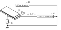
- FIG. 7 is a schematic diagram of a measurement environment for investigating the relationship between shield resistance and surface noise.
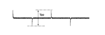
- FIG. 8A is a waveform diagram measured on the insulating sheet.
- FIG. 8B is a waveform diagram when the resistance of the variable resistor is 1000 ⁇ .
- FIG. 8A is a waveform diagram measured on the insulating sheet.
- FIG. 8B is a waveform diagram when the resistance of the variable resistor is 1000 ⁇ .
- FIG. 8C is a waveform diagram when the resistance of the variable resistor is 100 ⁇ .
- FIG. 8D is a waveform diagram when the resistance of the variable resistor is set to 0 ⁇ .
- FIG. 9 is a graph showing the relationship between the resistance of the variable resistor and the surface noise Vpp when various voltages are applied to the metal plate.
- FIG. 10 is a table showing the resistance values of the variable resistors that reduce the surface noise Vpp to 1 V or less when the resistance of the variable resistors is lowered while keeping the voltage applied to the metal plate constant.
- FIG. 11 is a graph of FIG.
- a display device is disposed on a first substrate, a second substrate disposed to face the first substrate, and a surface of the first substrate opposite to the second substrate. And a ground terminal electrically connected to the shield layer.
- the shield layer includes a transparent conductive film and a metal film disposed on at least a part of the peripheral edge of the first substrate in contact with the transparent conductive film.
- the maximum resistance from any point on the transparent conductive film to the ground terminal is defined as a shield resistance, the shield resistance is less than 1000 ⁇ , and the noise on the transparent conductive film is 1 V or less (first configuration) ).
- the display device includes the shield layer disposed on the surface of the first substrate opposite to the second substrate.
- the shield layer can shield an electric field from the second substrate side rather than the shield layer.
- the shield layer includes a transparent conductive film and a metal film. By placing the metal film on at least a part of the peripheral edge of the first substrate in contact with the transparent conductive film, the shield resistance can be lowered.
- the metal film is preferably arranged along one of the first side, the second side, and the third side of the first substrate (second configuration).
- the metal film is not disposed on at least one side of the first substrate. Therefore, the frame of the display device can be narrowed.
- the shield resistance is preferably 100 ⁇ or less (third configuration).
- a display device with a touch panel includes any one of the first to third display devices and a touch panel.
- FIG. 1 is a cross-sectional view showing a schematic configuration of a display device 100 with a touch panel according to an embodiment of the present invention.
- the display device 100 with a touch panel includes a display device 10, an OCA (Optical Clear Adhesive) 17, and a touch panel 18.
- the display device 10 and the touch panel 18 are bonded by the OCA 17.
- the display device 10 includes a first substrate 11, a second substrate 12, a liquid crystal layer 13, a shield layer 14, and polarizing plates 15 and 16.
- the first substrate 11 and the second substrate 12 are disposed to face each other.
- the liquid crystal layer 13 is disposed between the first substrate 11 and the second substrate 12.
- the shield layer 14 is disposed on the surface of the first substrate 11 opposite to the second substrate 12.
- the polarizing plate 15 is disposed on the shield layer 14.
- the polarizing plate 16 is disposed on the surface of the second substrate 12 opposite to the first substrate 11.
- a black matrix and a color filter are formed on the first substrate 11.
- FIG. 2 is a plan view showing a part of the second substrate 12 extracted.
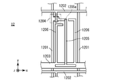
- a source line 1201, a gate line 1202, a capacitor line 1203, a TFT (Thin Film Transistor) 1204, a pixel electrode 1205, and a common electrode 1206 are formed on the second substrate 12.
- the gate line 1202 and the capacitor line 1203 are formed in parallel to each other.
- the source line 1201 is formed to be orthogonal to the gate line 1202 and the capacitor line 1203 in plan view.
- the TFT 1204 is formed in the vicinity of the intersection of the source line 1201 and the gate line 1202.
- the source of the TFT 1204 is connected to the source line 1201, and the gate is connected to the gate line 1202.
- the drain of the TFT 1204 is connected to the pixel electrode 1205 through the contact hole 1205a.
- the common electrode 1206 is connected to the capacitor line 1203. Note that an insulating layer (not shown) is formed between the pixel electrode 1205 and the capacitor line 1203 to form a storage capacitor.
- the liquid crystal display device 10 controls the alignment of the liquid crystal in the liquid crystal layer 13 by the potential difference between the pixel electrode 1205 and the common electrode 1206. That is, the display device 10 is an IPS (In Plane Switching) type liquid crystal display device that drives liquid crystal by an electric field in an in-plane direction.
- IPS In Plane Switching
- the shield layer 14 includes a transparent conductive film and a metal film, which will be described in detail later.
- the transparent conductive film and the metal film are films formed on the first substrate 11 by sputtering or the like.
- the shield layer 14 may be formed by forming a transparent conductive film and a metal film on a base material different from that of the first substrate 11 and superimposing the film on the first substrate 11.
- the touch panel 18 includes a substrate 180 and a sensor electrode 181 formed on the surface of the substrate 180 on the display device 10 side.
- the touch panel 18 detects a capacitance formed between a finger or the like close to the surface of the substrate 180 opposite to the display device 10 and the sensor electrode 181, and obtains the position of the finger or the like. That is, the touch panel 18 is a capacitive touch panel.
- the touch panel 18 is controlled by a touch panel controller (not shown).
- the touch panel controller is affected by noise from the display device 10.
- FIG. 3 is a graph showing the relationship between the touch panel drive frequency and the magnitude of noise received by the touch panel controller.
- pillars with a sand pattern indicate the magnitude of noise when the display device 10 has a low resolution
- shaded columns indicate the magnitude of noise when the display device 10 has a high resolution. ing.
- the touch panel drive frequency is used by selecting a frequency band in which the influence of noise from the display device 10 is small.
- the influence of noise from the display device 10 is reduced by the shield layer 14.
- FIG. 4 is a perspective view showing a schematic configuration of the display device 10.
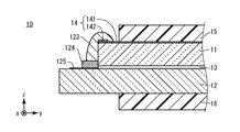
- FIG. 5 is a sectional view taken along line VV in FIG.
- the display device 10 further includes a source driver 121, a gate driver 122, a conductive paste 123, a ground pad 124, a ground wiring 125, and an FPC (Flexible Printed Circuit) 19.
- the transparent conductive film 141 and the metal film 142 of the shield layer 14 are hatched. Further, illustration of the polarizing plates 15 and 16 is omitted.
- the area of the second substrate 12 is larger than the area of the first substrate 11, and a part of the peripheral edge of the second substrate 12 is exposed.
- the source driver 121 and the gate driver 122 are mounted on the exposed peripheral portion of the second substrate 12 by a COG (Chip On Glass) technique. Note that the source driver 121 and the gate driver 122 may be implemented by TAB (Tape Automated Bonding) technology.
- the ground wiring 125 and other wiring are formed on the second substrate 12.
- the ground wiring 125 and other wiring form a ground terminal 125 a and other terminals (not shown) at the end of the second substrate 12.
- the ground terminal 125a and other terminals are connected to the FPC 19.
- a ground pad 124 is formed in contact with the ground wiring 125.
- the ground pad 124 is electrically connected to the shield layer 14 via the conductive paste 123.
- the shield layer 14 includes the transparent conductive film 141 and the metal film 142 as described above.
- the transparent conductive film 141 is formed so as to cover substantially the entire surface of the first substrate 11 opposite to the liquid crystal layer 13.
- the transparent conductive film 141 preferably has a high transmittance.
- the transparent conductive film 141 is, for example, ITO (Indium Tin Oxide).
- the transparent conductive film 141 is formed by sputtering or CVD (Chemical Vapor Deposition), for example.
- the metal film 142 is formed along two edges of the first substrate 11 in contact with the transparent conductive film 141. More specifically, the metal film 142 is formed on the first substrate 11 on the x-direction plus side edge in FIG. 4 and the y-direction minus side edge. The metal film 142 may be formed on at least a part of the peripheral edge of the first substrate 11. The metal film 142 is preferably formed outside the display area of the display device 10. Another example of the arrangement of the metal film 142 will be described later.
- the metal film 142 is, for example, an Ag alloy film.
- the metal film 142 is formed by sputtering, for example, and is patterned by photolithography.
- the transparent conductive film 141, the metal film 142, the conductive paste 123, the ground pad 124, the ground wiring 125, and the ground terminal 125a are electrically connected to each other.
- the maximum resistance value from any point on the transparent conductive film 141 to the ground terminal 125a is defined as a shield resistance.
- the resistance from the point P1 in FIG. 4 to the ground terminal 125a is theoretically maximum. Therefore, in this embodiment, the resistance from the point P1 to the ground terminal 125a is a shield resistance.
- the shield resistance of the display device 10 is less than 1000 ⁇ , preferably less than 100 ⁇ , and more preferably less than 50 ⁇ .
- the transparent conductive film 141, the metal film 142, the conductive paste 123, the ground pad 124, and the ground wiring 125 have low resistance.
- the sheet resistance of the transparent conductive film 141 is preferably 35 ⁇ / sq or less, more preferably 20 ⁇ / sq or less.
- the number of ground pads 124 is preferably large, and the area of each ground pad 124 is preferably large. Similarly, the cross-sectional area of the ground wiring 125 is preferably large.
- the metal film 142 is preferably wide. On the other hand, when the display device 10 is narrowed, it is not preferable to increase the width of the metal film 142.
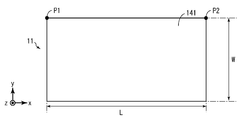
- FIG. 6A is a plan view showing an example of the arrangement of the metal film 142.
- a metal film 142A and a metal film 142B are formed instead of the metal film 142.
- the metal film 142A is formed along the negative side edge of the first substrate 11 in the x direction
- the metal film 142B is formed along the positive side edge in the x direction.
- FIG. 6B is a plan view showing the case where the metal film 142 is not provided.
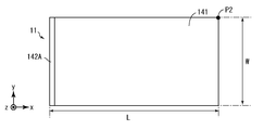
- FIG. 6C is a plan view showing another example of the arrangement of the metal film 142.
- a metal film 142A is formed instead of the metal film 142.
- FIG. 6D is a plan view showing another example of the arrangement of the metal film 142.
- a metal film 142C is formed instead of the metal film 142.
- the metal film 142 ⁇ / b> C is formed along the negative side edge of the first substrate 11 in the y direction.
- FIG. 6E is a plan view when the same metal film 142 as in FIG. 4 is formed.
- FIG. 6F is a plan view showing another example of the arrangement of the metal film 142.
- a metal film 142D is formed instead of the metal film 142.
- the metal film 142 ⁇ / b> D is formed along three end sides of the first substrate 11, that is, an end on the minus side in the y direction, an end on the plus side in the x direction, and an end on the plus side in the y direction.
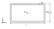
- FIG. 6G is a plan view showing another example of the arrangement of the metal film 142.
- a metal film 142E is formed instead of the metal film 142.
- the metal film 142E is formed along the four end sides of the first substrate 11.
- the number of edges forming the metal film is small. Note that when the metal film 142 is formed along the four edges of the first substrate 11 (in the case of the metal film 142E of FIG. 6G), there is a possibility that it becomes a loop antenna and amplifies noise.
- FIG. 7 is a schematic diagram of a measurement environment for this investigation.
- the insulating sheet 92 was disposed on the metal plate 93, and the conductive film 91 imitating the shield layer 14 was further disposed thereon.
- the conductive film 91 was grounded with the variable resistor 94 interposed therebetween.
- a rectangular wave imitating the drive pattern of the common electrode 1206 was generated by the pulse generator 95 and applied to the metal plate 93.
- a probe of an oscilloscope 96 was applied on the conductive film 91 or the insulating sheet 92, and the magnitude of the surface noise was measured.
- FIG. 8A to 8G are waveform diagrams when a 5 V rectangular wave is applied to the metal plate 93.
- FIG. 8A to 8G are waveform diagrams when a 5 V rectangular wave is applied to the metal plate 93.
- FIG. 8A is a waveform diagram measured on the insulating sheet 92. This waveform corresponds to the surface noise when the shield layer 14 is not provided in the display device 10.
- the surface noise Vpp (pp: Peak to Peak) was 10.2V.
- FIG. 8B is a waveform diagram when the resistance of the variable resistor 94 is 1000 ⁇ . This waveform corresponds to surface noise when the shield resistance of the display device 10 is 1000 ⁇ .
- the surface noise Vpp was 9.36V.
- FIG. 8C is a waveform diagram when the resistance of the variable resistor 94 is set to 100 ⁇ . This waveform corresponds to surface noise when the shield resistance of the display device 10 is 100 ⁇ .
- the surface noise Vpp was 5.92V.
- FIG. 8D is a waveform diagram when the resistance of the variable resistor 94 is set to 0 ⁇ . This waveform corresponds to the surface noise when the shield resistance is 0 ⁇ in the display device 10.
- the surface noise Vpp was 4.56V.
- the magnitude of the surface noise decreases as the resistance of the variable resistor 94 decreases. Further, as the resistance of the variable resistor 94 decreases, the time until the surface noise decreases becomes shorter. That is, in the display device 10, the lower the shield resistance, the smaller the size of the surface noise, and the shorter the time until the surface noise becomes smaller.
- the touch panel 18 can be driven during a period when the surface noise is small by driving the touch panel controller in synchronization with the display device 10.
- the following may be performed.
- A The resistance of the transparent conductive film 141, the metal film 142, the conductive paste 123, the ground pad 124, and the ground wiring 125 is lowered.
- B The number of ground pads 124 is increased. The area of the ground pad 124 is increased. The cross-sectional area of the ground wiring 125 is increased.
- C The metal film 142 is widened. The number of edges forming the metal film 142 is increased.
- (A) there is a limit to reducing the resistance depending on the material. Further, if the resistance is decreased by increasing the film thickness, the manufacturing time becomes longer and the manufacturing efficiency decreases.
- (B) is limited by the layout of wiring on the second substrate 12. In other words, if the number of the ground pads 124 is increased, the area of the ground pads 124 is increased, or the cross-sectional area of the ground wiring 125 is increased, the degree of freedom in designing the second substrate 12 decreases. .
- (C) as the width of the metal film 142 is increased or the number of edges forming the metal film 142 is increased, it is difficult to narrow the frame.
- FIG. 9 is a graph showing the relationship between the resistance of the variable resistor 94 and the surface noise Vpp when rectangular waves having various amplitudes are applied to the metal plate 93. This corresponds to the relationship between the shield resistance for each noise level and the surface noise Vpp in the display device 10.
- variable resistance when a rectangular wave having an amplitude such that the surface noise Vpp is 1.8V when the value of the variable resistance is 1000 ⁇ , the variable resistance is set to 20 ⁇ or less in order to reduce the surface noise Vpp to 1V or less. You can see that Similarly, when a rectangular wave having an amplitude such that the surface noise Vpp is 1.7 V when the value of the variable resistance is 1000 ⁇ , the variable resistance should be 40 ⁇ or less in order to reduce the surface noise Vpp to 1 V or less. You can see that
- FIG. 10 is a table showing the resistance values of the variable resistor 94 that reduces the surface noise Vpp to 1 V or less when the resistance of the variable resistor 94 is lowered while keeping the amplitude of the rectangular wave applied to the metal plate 93 constant. It is.
- FIG. 11 is a graph of FIG.
- the shield resistance should be less than 1000 ⁇ .
- the display device 10 may be designed.
- the shield resistance may be designed to be less than 700 ⁇ . If the noise level is higher than 1.10V and not higher than 1.15V, the shield resistance may be less than 500 ⁇ . If the noise level is higher than 1.10V and not higher than 1.15V, the shield resistance may be less than 400 ⁇ . If the noise level is higher than 1.20V and not higher than 1.35V, the shield resistance should be less than 300 ⁇ . If the noise level is higher than 1.35V and lower than 1.50V, the shield resistance may be less than 200 ⁇ . If the noise level is higher than 1.50V and not higher than 1.65V, the shield resistance should be less than 100 ⁇ .
- the shield resistance should be less than 80 ⁇ . If the noise level is higher than 1.70V and lower than 1.75V, the shield resistance should be less than 60 ⁇ . If the noise level is higher than 1.75V and lower than 1.80V, the shield resistance should be less than 40 ⁇ . If the noise level is higher than 1.80V, the shield resistance should be less than 20 ⁇ .
- a prototype of the display device 10 is produced, and the values of the shield resistance and the surface noise Vpp are measured. Then, based on FIGS. 9 to 11, the value of the shield resistance at which the surface noise Vpp of the display device 10 is 1 V or less is obtained. Then, (A) the resistance of the transparent conductive film 141, the metal film 142, the conductive paste 123, the ground pad 124, and the ground wiring 125, and (B) the number of the ground pads 124 so that the obtained shield resistance value is obtained. The area of the ground pad 124, the cross-sectional area of the ground wiring 125, (C) the width of the metal film 142, the number of edges forming the metal film 142, and the like may be adjusted.
- (A) to (C) may be adjusted so that the shield resistance is 500 ⁇ or less.
- a curve C1 in FIG. 11 shows the relationship between the 2-section moving average of the shield resistance for the surface noise Vpp to be 1V or less and the noise level of the display device 10.
- the shield resistance is preferably less than 100 ⁇ .
- the shield resistance is more preferably less than 50 ⁇ .
- the display device is an IPS liquid crystal display device.
- the driving method of the display device is not limited to the IPS method.
- the display device may be, for example, a liquid crystal display device having a common electrode on the first substrate.
- the present invention is not limited to the liquid crystal display device, and can be applied to various display devices in which two substrates are arranged to face each other.
- the present invention can be used industrially as a display device and a display device with a touch panel.
Landscapes
- Engineering & Computer Science (AREA)
- Physics & Mathematics (AREA)
- Theoretical Computer Science (AREA)
- General Engineering & Computer Science (AREA)
- General Physics & Mathematics (AREA)
- Human Computer Interaction (AREA)
- Nonlinear Science (AREA)
- Crystallography & Structural Chemistry (AREA)
- Optics & Photonics (AREA)
- Chemical & Material Sciences (AREA)
- Mathematical Physics (AREA)
- Liquid Crystal (AREA)
- Devices For Indicating Variable Information By Combining Individual Elements (AREA)
Abstract
駆動ノイズを低減し、高精度のタッチパネルと組み合わせることができる表示装置を得る。表示装置(10)は、第1基板(11)と、第1基板(11)に対向して配置される第2基板(12)と、第1基板(11)の第2基板(12)と反対側の面に配置されるシールド層(14)と、シールド層(14)に電気的に接続されるグランド端子(125a)とを備える。シールド層(14)は、透明導電膜(141)と、透明導電膜(141)に接して、第1基板(11)の周縁部の少なくとも一部に配置される金属膜(142)とを含む。透明導電膜(141)上の任意の点からグランド端子(125a)までの抵抗の最大値をシールド抵抗とし、シールド抵抗は1000Ω未満であり、透明導電膜上のノイズが1V以下である。
Description
本発明は、表示装置およびタッチパネル付き表示装置に関する。
タッチパネル付き表示装置の薄型化に伴い、表示装置の駆動ノイズがタッチパネルコントローラに伝わり、タッチパネルのSN比が低下する。SN比の低下によって、ペン入力、ホバー入力といった機能を実現することが困難になる。
特開2011-95451号公報には、静電シールドとしての導電膜を備える横電界方式の液晶表示装置が開示されている。
特開2011-95451号公報に開示された構成では、透明導電膜が高抵抗であるため、充分な遮蔽効果を得ることができない。
本発明の目的は、駆動ノイズを低減し、高精度のタッチパネルと組み合わせることができる表示装置、およびタッチパネル付き表示装置を提供することである。
ここに開示する表示装置は、第1基板と、前記第1基板に対向して配置される第2基板と、前記第1基板の前記第2基板と反対側の面に配置されるシールド層と、前記シールド層に電気的に接続されるグランド端子とを備える。前記シールド層は、透明導電膜と、前記透明導電膜に接して、前記第1基板の周縁部の少なくとも一部に配置される金属膜とを含む。前記透明導電膜上の任意の点から前記グランド端子までの抵抗の最大値をシールド抵抗とし、前記シールド抵抗は1000Ω未満であり、前記透明導電膜上のノイズが1V以下である。
本発明によれば、駆動ノイズを低減し、高精度のタッチパネルと組み合わせることができる表示装置、およびタッチパネル付き表示装置が得られる。
本発明の一実施形態にかかる表示装置は、第1基板と、前記第1基板に対向して配置される第2基板と、前記第1基板の前記第2基板と反対側の面に配置されるシールド層と、前記シールド層に電気的に接続されるグランド端子とを備える。前記シールド層は、透明導電膜と、前記透明導電膜に接して、前記第1基板の周縁部の少なくとも一部に配置される金属膜とを含む。前記透明導電膜上の任意の点から前記グランド端子までの抵抗の最大値をシールド抵抗とし、前記シールド抵抗は1000Ω未満であり、前記透明導電膜上のノイズが1V以下である(第1の構成)。
上記の構成によれば、表示装置は、第1基板の第2基板と反対側の面に配置されたシールド層を備える。シールド層によって、シールド層よりも第2基板側からの電界を遮蔽することができる。シールド層は、透明導電膜と、金属膜とを含む。透明導電膜に接して第1基板の周縁部の少なくとも一部に金属膜を配置することで、シールド抵抗を低くすることができる。
上記第1の構成において、前記金属膜は、前記第1基板の1辺、2辺、および3辺のいずれかに沿って配置されることが好ましい(第2の構成)。
上記の構成によれば、第1基板の少なくとも1辺には金属膜が配置されない。これによって、表示装置の額縁を狭くできる。
上記第1または第2の構成において、前記シールド抵抗は100Ω以下であることが好ましい(第3の構成)。
本発明の一実施形態にかかるタッチパネル付き表示装置は、上記第1~第3のいずれかの表示装置と、タッチパネルとを備える。
[実施の形態]
以下、図面を参照し、本発明の実施の形態を詳しく説明する。図中同一または相当部分には同一符号を付してその説明は繰り返さない。なお、説明を分かりやすくするために、以下で参照する図面においては、構成が簡略化または模式化して示されたり、一部の構成部材が省略されたりしている。また、各図に示された構成部材間の寸法比は、必ずしも実際の寸法比を示すものではない。
以下、図面を参照し、本発明の実施の形態を詳しく説明する。図中同一または相当部分には同一符号を付してその説明は繰り返さない。なお、説明を分かりやすくするために、以下で参照する図面においては、構成が簡略化または模式化して示されたり、一部の構成部材が省略されたりしている。また、各図に示された構成部材間の寸法比は、必ずしも実際の寸法比を示すものではない。
図1は、本発明の一実施形態にかかるタッチパネル付き表示装置100の概略構成を示す断面図である。タッチパネル付き表示装置100は、表示装置10と、OCA(Optical Clear Adhesive)17と、タッチパネル18とを備えている。表示装置10とタッチパネル18とは、OCA17によって接着されている。
表示装置10は、第1基板11、第2基板12、液晶層13、シールド層14、ならびに偏光板15および16を備えている。第1基板11と第2基板12とは、互いに対向して配置されている。液晶層13は、第1基板11と第2基板12との間に配置されている。シールド層14は、第1基板11の第2基板12と反対側の面に配置されている。偏光板15は、シールド層14の上に配置されている。偏光板16は、第2基板12の第1基板11と反対側の面に配置されている。
詳しい構成は図示しないが、第1基板11には、ブラックマトリクスと、カラーフィルタとが形成されている。
図2は、第2基板12の一部を抜き出して示す平面図である。第2基板12には、ソース線1201、ゲート線1202、容量線1203、TFT(Thin Film Transistor)1204、画素電極1205、および共通電極1206が形成されている。
ゲート線1202と容量線1203とは、互いに平行に形成されている。ソース線1201は、ゲート線1202および容量線1203と、平面視において直交するように形成されている。TFT1204は、ソース線1201とゲート線1202との交点近傍に形成されている。TFT1204のソースはソース線1201に接続されており、ゲートはゲート線1202に接続されている。TFT1204のドレインは、コンタクトホール1205aを介して、画素電極1205に接続されている。
共通電極1206は、容量線1203に接続されている。なお、画素電極1205と容量線1203との間には絶縁層(不図示)が形成されており、蓄積容量を形成している。
液晶表示装置10は、画素電極1205と共通電極1206との間の電位差によって液晶層13の液晶の配向を制御する。すなわち、表示装置10は、面内方向の電界によって液晶を駆動する、IPS(In Plane Switching)方式の液晶表示装置である。
シールド層14は、詳しい構成は後述するが、透明導電膜と、金属膜とを含んでいる。本実施形態では、透明導電膜および金属膜は、スパッタリング等によって第1基板11上に成膜された膜である。なお、シールド層14は、第1基板11とは別の基材に透明導電膜および金属膜を形成し、これを第1基板11に重ね合わせたものであっても良い。
タッチパネル18は、基板180と、基板180の表示装置10側の面に形成されたセンサ電極181とを備えている。タッチパネル18は、基板180の表示装置10と反対側の面に近接した指等と、センサ電極181との間に形成される静電容量を検出し、指等の位置を求める。すなわち、タッチパネル18は、静電容量方式のタッチパネルである。
タッチパネル18は、図示しないタッチパネルコントローラによって制御される。タッチパネルコントローラは、表示装置10からのノイズの影響を受ける。図3は、タッチパネル駆動周波数と、タッチパネルコントローラが受けるノイズの大きさとの関係を示すグラフである。図3中、砂地模様を付した柱は表示装置10が低解像度の場合のノイズの大きさを示しており、斜線を付した柱は表示装置10が高解像度の場合のノイズの大きさを示している。
タッチパネル駆動周波数は、表示装置10からのノイズの影響が小さい周波数帯を選択して用いられる。しかし、図3に示すように、表示装置10を高解像度化すると、全ての周波数帯においてノイズが増大し、ノイズの影響の小さい周波数帯が存在しなくなる。そこで、本実施形態では、シールド層14によって、表示装置10からのノイズの影響を低減する。
図4は、表示装置10の概略構成を示す斜視図である。図5は、図4のV-V線に沿った断面図である。表示装置10は、ソースドライバ121、ゲートドライバ122、導電性ペースト123、グランドパッド124、グランド配線125、およびFPC(Flexible Printed Circuit)19をさらに備えている。なお、図4では、シールド層14の透明導電膜141および金属膜142にハッチングを付して示している。また、偏光板15および16の図示を省略している。
図4に示すように、第2基板12の面積は第1基板11の面積よりも大きく、第2基板12の周縁部の一部が露出している。ソースドライバ121およびゲートドライバ122は、第2基板12の露出した周縁部に、COG(Chip On Glass)技術によって実装されている。なお、ソースドライバ121およびゲートドライバ122は、TAB(Tape Automated Bonding)技術によって実装されたものであっても良い。
第2基板12には、グランド配線125、および図示しない他の配線が形成されている。グランド配線125および他の配線は、第2基板12の端部においてグランド端子125aおよび図示しない他の端子を形成している。グランド端子125aおよび他の端子は、FPC19と接続される。
グランド配線125に接して、グランドパッド124が形成されている。グランドパッド124は、導電性ペースト123を介してシールド層14と電気的に接続している。
シールド層14は、既述のように、透明導電膜141と、金属膜142とを含んでいる。
透明導電膜141は、第1基板11の、液晶層13と反対側の面の概略全面を覆って形成されている。透明導電膜141は、透過率が高いことが好ましい。透明導電膜141は、例えばITO(Indium Tin Oxide)である。透明導電膜141は、例えばスパッタリングまたはCVD(Chemical Vapor Deposition)によって成膜される。
金属膜142は、透明導電膜141に接して、第1基板11の2つの端辺に沿って形成されている。より具体的には、金属膜142は、第1基板11の、図4におけるx方向プラス側の端辺とy方向マイナス側の端辺とに形成されている。なお、金属膜142は、第1基板11の周縁部の少なくとも一部に形成されていれば良い。金属膜142は、好ましくは、表示装置10の表示領域の外側に形成される。金属膜142の配置の他の例については後述する。金属膜142は、例えばAg合金の膜である。金属膜142は、例えばスパッタリングによって成膜され、フォトリソグラフィによってパターニングされる。
以上の構成により、透明導電膜141、金属膜142、導電性ペースト123、グランドパッド124、グランド配線125、およびグランド端子125aが、相互に電気的に接続している。
ここで、透明導電膜141上の任意の点からグランド端子125aまでの抵抗の最大値を、シールド抵抗と定義する。本実施形態の場合、図4の点P1からグランド端子125aまでの抵抗が、理論上最大となる。したがって本実施形態の場合、点P1からグランド端子125aまでの抵抗が、シールド抵抗である。
表示装置10のシールド抵抗は、詳しくは後述するが、1000Ω未満であり、好ましくは100Ω未満であり、さらに好ましくは50Ω未満である。
シールド抵抗を低くするため、透明導電膜141、金属膜142、導電性ペースト123、グランドパッド124、およびグランド配線125の抵抗は、低いことが好ましい。
透明導電膜141のシート抵抗は、好ましくは35Ω/sq以下であり、さらに好ましくは20Ω/sq以下である。
グランドパッド124の数は多いことが好ましく、各グランドパッド124の面積は大きいことが好ましい。同様に、グランド配線125の断面積は大きいことが好ましい。
シールド抵抗を低くするうえでは、金属膜142の幅は広いことが好ましい。一方、表示装置10を狭額縁化するうえでは、金属膜142の幅を広くすることは好ましくない。
以下、図6A~図6Gを参照して、金属膜142の配置と、シールド抵抗との関係を説明する。
図6Aは、金属膜142の配置の一例を示す平面図である。図6Aでは、金属膜142に代えて、金属膜142Aと金属膜142Bとが形成されている。金属膜142Aは第1基板11のx方向マイナス側の端辺に沿って形成され、金属膜142Bはx方向プラス側の端辺に沿って形成されている。
このとき、第1基板11のx方向の寸法をL、y方向の寸法をW、透明導電膜141の抵抗率をρ、透明導電膜141の厚さをtとすると、金属膜142Aから金属膜142Bまでの間の抵抗Rは、R=ρ×L/(W・t)となる。なお、シート抵抗ρs=ρ/tを用いると、上式はR=ρs×L/Wとなる。
例えば、W=64mm、L=122mm、ρ=2.8×10⁻⁶Ωcm-1、t=140nmの場合、R≒38Ωである。
図6Bは、金属膜142がない場合を示す平面図である。この場合、点P1から点P2までの間の抵抗R1は、R1=3.43×R≒131Ωである。
図6Cは、金属膜142の配置の他の例を示す平面図である。図6Cでは、金属膜142に代えて、金属膜142Aが形成されている。この場合、点P2から金属膜142Aまでの間の抵抗R2は、R2=1.81×R≒69Ωである。
図6Dは、金属膜142の配置の他の例を示す平面図である。図6Dでは、金属膜142に代えて、金属膜142Cが形成されている。金属膜142Cは、第1基板11のy方向マイナス側の端辺に沿って形成されている。この場合、点P2から金属膜142Cまでの間の抵抗R3は、R3=0.88×R≒34Ωである。
図6Eは、図4と同じ金属膜142が形成された場合の平面図である。この場合、点P1から金属膜142までの間の抵抗R4は、R4=0.59×R≒22Ωである。
図6Fは、金属膜142の配置の他の例を示す平面図である。図6Fでは、金属膜142に代えて、金属膜142Dが形成されている。金属膜142Dは、第1基板11のy方向マイナス側の端辺と、x方向プラス側の端辺と、y方向プラス側の端辺との、3つの端辺に沿って形成されている。この場合、点P3から金属膜142Dまでの間の抵抗R5は、R5=0.16×R≒6.1Ωである。
図6Gは、金属膜142の配置の他の例を示す平面図である。図6Gでは、金属膜142に代えて、金属膜142Eが形成されている。金属膜142Eは、第1基板11の4つの端辺に沿って形成されている。この場合、点P4から金属膜142Eまでの間の抵抗R6は、R6=0.1×R≒3.8Ωである。
以上のように、金属膜を形成する端辺の数が多いほど、抵抗は低くなる。一方、表示装置10を狭額縁化するうえでは、金属膜を形成する端辺の数は少ない方が好ましい。なお、金属膜142を第1基板11の4つの端辺に沿って形成する場合(図6Gの金属膜142Eの場合)、ループアンテナとなってノイズを増幅する可能性が有る。
本発明者は、以下のように、シールド抵抗と表面ノイズとの関係を調査した。図7は、この調査のための測定環境の模式図である。図7に示すように、金属板93の上に絶縁シート92を配置し、さらにその上にシールド層14に模した導電膜91を配置した。導電膜91は、可変抵抗94を間に介して接地した。パルスジェネレータ95によって共通電極1206の駆動パターンを模した矩形波を発生させ、金属板93に印加した。導電膜91または絶縁シート92の上にオシロスコープ96のプローブをあてて、表面ノイズの大きさを測定した。
図8A~図8Gは、金属板93に5Vの矩形波を印加したときの波形図である。
図8Aは、絶縁シート92の上を測定した波形図である。この波形は、表示装置10においてシールド層14がない場合の表面ノイズに相当する。表面ノイズVpp(pp:Peak to Peak)は、10.2Vであった。
図8Bは、可変抵抗94の抵抗を1000Ωにした場合の波形図である。この波形は、表示装置10においてシールド抵抗が1000Ωである場合の表面ノイズに相当する。表面ノイズVppは、9.36Vであった。
図8Cは、可変抵抗94の抵抗を100Ωにした場合の波形図である。この波形は、表示装置10においてシールド抵抗が100Ωである場合の表面ノイズに相当する。表面ノイズVppは、5.92Vであった。
図8Dは、可変抵抗94の抵抗を0Ωにした場合の波形図である。この波形は、表示装置10においてシールド抵抗が0Ωである場合の表面ノイズに相当する。表面ノイズVppは、4.56Vであった。
以上のように、可変抵抗94の抵抗が小さくなるにしたがって、表面ノイズの大きさは小さくなる。また、可変抵抗94の抵抗が小さくなるにしたがって、表面ノイズが小さくなるまでの時間が短くなる。すなわち、表示装置10において、シールド抵抗が低いほど、表面ノイズの大きさが小さくなり、表面ノイズが小さくなるまでの時間が短くなる。
なお、表面ノイズが小さくなるまでの時間が短ければ、表面ノイズが小さい期間が長くなる。そのため、表面ノイズが小さくなるまでの時間を短くすることできれば、タッチパネルコントローラを表示装置10と同期して駆動することで、表面ノイズが小さい期間にタッチパネル18を駆動することができる。
シールド抵抗を低くするためには、例えば、次のようにすれば良い。(A)透明導電膜141、金属膜142、導電性ペースト123、グランドパッド124、およびグランド配線125の抵抗を低くする。(B)グランドパッド124の数を多くする。グランドパッド124の面積を大きくする。グランド配線125の断面積を大きくする。(C)金属膜142の幅を広くする。金属膜142を形成する端辺の数を多くする。
しかしながら、(A)については、材料によって抵抗を低くすることには限界がある。また、膜厚を厚くして抵抗を下げようとすれば、製造時間が長くなり、製造効率が低下する。(B)については、第2基板12上の配線のレイアウトによって制限される。換言すれば、グランドパッド124の数を多くしたり、グランドパッド124の面積を大きくしたり、またはグランド配線125の断面積を大きくしたりすれば、第2基板12の設計の自由度が低下する。(C)については、金属膜142の幅を広くするほど、あるいは金属膜142を形成する端辺の数を多くするほど、狭額縁化が困難になる。
これらの理由から、シールド抵抗を必要以上に低くすることは合理的ではない。以下では、表面ノイズを1V以下にするために必要なシールド抵抗の値を検討する。
表面ノイズを1V以下にするために必要なシールド抵抗の値は、発生するノイズの大きさ(ノイズレベル)に依存する。再び図7の測定環境を用いて、様々なノイズレベルのもとで、表面ノイズを1V以下にするためのシールド抵抗の値を調査した。図9は、種々の振幅の矩形波を金属板93に印加した場合における、可変抵抗94の抵抗と表面ノイズVppとの関係を示すグラフである。これは、表示装置10における、ノイズレベルごとのシールド抵抗と表面ノイズVppとの関係に相当する。
図9から、可変抵抗の値が1000Ωのときに表面ノイズVppが1.8Vとなるような振幅の矩形波を印加した場合、表面ノイズVppを1V以下にするためには、可変抵抗を20Ω以下にすれば良いことが分かる。同様に、可変抵抗の値が1000Ωのときに表面ノイズVppが1.7Vとなるような振幅の矩形波を印加した場合、表面ノイズVppを1V以下にするためには、可変抵抗を40Ω以下にすれば良いことが分かる。
図10は、金属板93に印加する矩形波の振幅を一定にして可変抵抗94の抵抗を下げていったとき、表面ノイズVppを1V以下にする可変抵抗94の抵抗の値を表にしたものである。図11は、図10をグラフにしたものである。
図10および図11から、ノイズレベルが1.00Vよりも高く1.05V以下のときに、表示装置10の表面ノイズの大きさを1V以下にするためには、シールド抵抗が1000Ω未満になるように表示装置10を設計すれば良い。
同様に、ノイズレベルが1.05Vよりも高く1.10V以下であれば、シールド抵抗が700Ω未満になるように設計すれば良い。ノイズレベルが1.10Vよりも高く1.15V以下であれば、シールド抵抗が500Ω未満になるようにすれば良い。ノイズレベルが1.10Vよりも高く1.15V以下であれば、シールド抵抗が400Ω未満になるようにすれば良い。ノイズレベルが1.20Vよりも高く1.35V以下であれば、シールド抵抗が300Ω未満になるようにすれば良い。ノイズレベルが1.35Vよりも高く1.50V以下であれば、シールド抵抗が200Ω未満になるようにすれば良い。ノイズレベルが1.50Vよりも高く1.65V以下であれば、シールド抵抗が100Ω未満になるようにすれば良い。ノイズレベルが1.65Vよりも高く1.70V以下であれば、シールド抵抗が80Ω未満になるようにすれば良い。ノイズレベルが1.70Vよりも高く1.75V以下であれば、シールド抵抗が60Ω未満になるようにすれば良い。ノイズレベルが1.75Vよりも高く1.80V以下であれば、シールド抵抗が40Ω未満になるようにすれば良い。ノイズレベルが1.80Vよりも高ければ、シールド抵抗が20Ω未満になるようにすれば良い
より具体的には、まず表示装置10の試作品を作製し、シールド抵抗と、表面ノイズVppの値を測定する。そして、図9~図11に基づき、表示装置10の表面ノイズVppが1V以下になるシールド抵抗の値を求める。そして、求められたシールド抵抗の値になるように、(A)透明導電膜141、金属膜142、導電性ペースト123、グランドパッド124、およびグランド配線125の抵抗、(B)グランドパッド124の数、グランドパッド124の面積、グランド配線125の断面積、(C)金属膜142の幅、金属膜142を形成する端辺の数などを調整すれば良い。
例えば、試作品のシールド抵抗が1000Ω、表面ノイズが1.10Vの場合、シールド抵抗が500Ω以下となるように、(A)~(C)を調整すれば良い。
図11中の曲線C1は、表面ノイズVppが1V以下になるためのシールド抵抗の2区間移動平均と、表示装置10のノイズレベルとの関係を示している。図11に示すように、シールド抵抗を100Ω未満とすることで、遮蔽効果が急激に上昇する。したがって、シールド抵抗は、好ましくは100Ω未満である。シールド抵抗は、さらに好ましくは、50Ω未満である。
[その他の実施形態]
以上、本発明についての実施形態を説明したが、本発明は上述の実施形態に限定されず、発明の範囲内で種々の変更が可能である。
以上、本発明についての実施形態を説明したが、本発明は上述の実施形態に限定されず、発明の範囲内で種々の変更が可能である。
上述の実施形態では、表示装置がIPS方式の液晶表示装置である場合を説明した。しかし、表示装置の駆動方式はIPS方式に限定されない。表示装置は、例えば、第1基板に共通電極を備えた液晶表示装置であっても良い。また、本発明は液晶表示装置に限定されず、2枚の基板が対向して配置される様々な表示装置に適用可能である。
本発明は、表示装置およびタッチパネル付き表示装置として産業上の利用が可能である。
Claims (4)
- 第1基板と、
前記第1基板に対向して配置される第2基板と、
前記第1基板の前記第2基板と反対側の面に配置されるシールド層と、
前記シールド層に電気的に接続されるグランド端子とを備え、
前記シールド層は、
透明導電膜と、
前記透明導電膜に接して、前記第1基板の周縁部の少なくとも一部に配置される金属膜とを含み、
前記透明導電膜上の任意の点から前記グランド端子までの抵抗の最大値をシールド抵抗とし、前記シールド抵抗は1000Ω未満であり、
前記透明導電膜上のノイズが1V以下である、表示装置。 - 前記透明導電膜は矩形であり、
前記金属膜は、前記第1基板の1辺、2辺、および3辺のいずれかに沿って配置される、請求項1に記載の表示装置。 - 前記シールド抵抗は100Ω以下である、請求項1または2に記載の表示装置。
- 請求項1~3のいずれか一項に記載の表示装置と、
タッチパネルとを備える、タッチパネル付き表示装置。
Priority Applications (1)
| Application Number | Priority Date | Filing Date | Title |
|---|---|---|---|
| US14/651,177 US20150316812A1 (en) | 2012-12-14 | 2013-12-09 | Display device and touch panel-equipped display device |
Applications Claiming Priority (2)
| Application Number | Priority Date | Filing Date | Title |
|---|---|---|---|
| JP2012273976 | 2012-12-14 | ||
| JP2012-273976 | 2012-12-14 |
Publications (1)
| Publication Number | Publication Date |
|---|---|
| WO2014092049A1 true WO2014092049A1 (ja) | 2014-06-19 |
Family
ID=50934338
Family Applications (1)
| Application Number | Title | Priority Date | Filing Date |
|---|---|---|---|
| PCT/JP2013/082969 Ceased WO2014092049A1 (ja) | 2012-12-14 | 2013-12-09 | 表示装置およびタッチパネル付き表示装置 |
Country Status (2)
| Country | Link |
|---|---|
| US (1) | US20150316812A1 (ja) |
| WO (1) | WO2014092049A1 (ja) |
Cited By (3)
| Publication number | Priority date | Publication date | Assignee | Title |
|---|---|---|---|---|
| US9541961B1 (en) | 2015-08-25 | 2017-01-10 | Microsoft Technology Licensing, Llc | Shielding via display chassis |
| JP2018097869A (ja) * | 2016-12-09 | 2018-06-21 | エルジー ディスプレイ カンパニー リミテッド | 電子機器 |
| US12321554B2 (en) | 2021-03-31 | 2025-06-03 | Chengdu Boe Optoelectronics Technology Co. , Ltd. | Touch substrate, touch module, and display device |
Families Citing this family (5)
| Publication number | Priority date | Publication date | Assignee | Title |
|---|---|---|---|---|
| WO2017010291A1 (ja) * | 2015-07-13 | 2017-01-19 | 三菱電機株式会社 | 表示装置 |
| US10402019B2 (en) * | 2015-10-31 | 2019-09-03 | Lg Display Co., Ltd. | Display device |
| CN105786244B (zh) * | 2016-02-04 | 2019-02-15 | 京东方科技集团股份有限公司 | 一种显示模组、显示装置 |
| TWI694362B (zh) * | 2018-12-27 | 2020-05-21 | 友達光電股份有限公司 | 觸控顯示器 |
| CN111258457B (zh) * | 2020-01-21 | 2021-10-19 | 京东方科技集团股份有限公司 | 一种触控显示装置 |
Citations (4)
| Publication number | Priority date | Publication date | Assignee | Title |
|---|---|---|---|---|
| JPH1154984A (ja) * | 1997-07-31 | 1999-02-26 | Kenwood Corp | 電気部品の電磁波シールド構造 |
| JP2008218142A (ja) * | 2007-03-02 | 2008-09-18 | Seiko Epson Corp | 入力機能付有機エレクトロルミネッセンス装置、及び電子機器 |
| JP2009086184A (ja) * | 2007-09-28 | 2009-04-23 | Casio Comput Co Ltd | タッチパネル付き液晶表示装置 |
| JP2011248694A (ja) * | 2010-05-28 | 2011-12-08 | Wacom Co Ltd | 指示体検出装置 |
Family Cites Families (6)
| Publication number | Priority date | Publication date | Assignee | Title |
|---|---|---|---|---|
| JP5207728B2 (ja) * | 2006-12-21 | 2013-06-12 | 富士フイルム株式会社 | 導電膜およびその製造方法 |
| US20080309633A1 (en) * | 2007-06-13 | 2008-12-18 | Apple Inc. | Touch-sensitive display |
| TW200921483A (en) * | 2007-11-09 | 2009-05-16 | Tpk Touch Solutions Inc | Touch-control display panel with an electric-field shielding layer |
| US8576574B2 (en) * | 2010-04-21 | 2013-11-05 | Stmicroelectronics Pte Ltd. | Electromagnetic interference shielding on semiconductor devices |
| KR101706232B1 (ko) * | 2010-06-29 | 2017-02-15 | 엘지디스플레이 주식회사 | 터치 패널 |
| KR20130005660A (ko) * | 2011-07-07 | 2013-01-16 | 삼성전자주식회사 | 터치스크린패널 액정디스플레이장치 |
-
2013
- 2013-12-09 US US14/651,177 patent/US20150316812A1/en not_active Abandoned
- 2013-12-09 WO PCT/JP2013/082969 patent/WO2014092049A1/ja not_active Ceased
Patent Citations (4)
| Publication number | Priority date | Publication date | Assignee | Title |
|---|---|---|---|---|
| JPH1154984A (ja) * | 1997-07-31 | 1999-02-26 | Kenwood Corp | 電気部品の電磁波シールド構造 |
| JP2008218142A (ja) * | 2007-03-02 | 2008-09-18 | Seiko Epson Corp | 入力機能付有機エレクトロルミネッセンス装置、及び電子機器 |
| JP2009086184A (ja) * | 2007-09-28 | 2009-04-23 | Casio Comput Co Ltd | タッチパネル付き液晶表示装置 |
| JP2011248694A (ja) * | 2010-05-28 | 2011-12-08 | Wacom Co Ltd | 指示体検出装置 |
Cited By (5)
| Publication number | Priority date | Publication date | Assignee | Title |
|---|---|---|---|---|
| US9541961B1 (en) | 2015-08-25 | 2017-01-10 | Microsoft Technology Licensing, Llc | Shielding via display chassis |
| US10156872B2 (en) | 2015-08-25 | 2018-12-18 | Microsoft Technology Licensing, Llc | Shielding via display chassis |
| JP2018097869A (ja) * | 2016-12-09 | 2018-06-21 | エルジー ディスプレイ カンパニー リミテッド | 電子機器 |
| US10720474B2 (en) | 2016-12-09 | 2020-07-21 | Lg Display Co., Ltd. | Electronic device |
| US12321554B2 (en) | 2021-03-31 | 2025-06-03 | Chengdu Boe Optoelectronics Technology Co. , Ltd. | Touch substrate, touch module, and display device |
Also Published As
| Publication number | Publication date |
|---|---|
| US20150316812A1 (en) | 2015-11-05 |
Similar Documents
| Publication | Publication Date | Title |
|---|---|---|
| WO2014092049A1 (ja) | 表示装置およびタッチパネル付き表示装置 | |
| CN102436323B (zh) | 嵌有触摸面板的显示设备及其制造方法 | |
| CN105765498B (zh) | 带触摸传感器的显示装置 | |
| EP4095657B1 (en) | Touch display device | |
| US8847908B2 (en) | Display device | |
| KR102404552B1 (ko) | 플렉스 회로를 갖는 터치 센서 패널에 대한 트레이스 전사 기법 | |
| TWI461792B (zh) | 具有內建觸控螢幕面板的液晶顯示器 | |
| US20160378240A1 (en) | 3d module, 3d display device and method for driving 3d module | |
| CN101910984A (zh) | 触摸面板和包括该触摸面板的显示装置 | |
| US20180373091A1 (en) | Display panel | |
| CN102262469A (zh) | 触控面板、触控显示面板及触控面板的制作方法 | |
| CN107688252A (zh) | 内嵌式触控液晶显示面板 | |
| CN108572757A (zh) | 触控面板及其制作方法、触控显示装置 | |
| CN106257324A (zh) | 内嵌式触控显示装置 | |
| JP2019184721A (ja) | 表示装置 | |
| JP2010117955A (ja) | 表示装置 | |
| US9036110B2 (en) | Display apparatus and method of manufacturing the same | |
| KR101859469B1 (ko) | 표시 장치 및 그의 제조 방법 | |
| JP4501933B2 (ja) | 液晶表示装置 | |
| JP2011186623A (ja) | タッチパネル付き表示装置 | |
| WO2013161868A1 (ja) | タッチパネル付き表示装置 | |
| CN106547151B (zh) | 触控显示面板结构 | |
| KR20150087941A (ko) | 전극부재, 이를 포함하는 터치 윈도우 및 이를 포함하는 디스플레이 장치 | |
| KR102237941B1 (ko) | 터치 윈도우 | |
| CN222994788U (zh) | 一种tft液晶显示屏、显示终端及电子设备 |
Legal Events
| Date | Code | Title | Description |
|---|---|---|---|
| 121 | Ep: the epo has been informed by wipo that ep was designated in this application |
Ref document number: 13861951 Country of ref document: EP Kind code of ref document: A1 |
|
| WWE | Wipo information: entry into national phase |
Ref document number: 14651177 Country of ref document: US |
|
| NENP | Non-entry into the national phase |
Ref country code: DE |
|
| 122 | Ep: pct application non-entry in european phase |
Ref document number: 13861951 Country of ref document: EP Kind code of ref document: A1 |
|
| NENP | Non-entry into the national phase |
Ref country code: JP |