WO2014084358A1 - 有機el素子並びにそれを備えた画像表示装置及び照明装置 - Google Patents
有機el素子並びにそれを備えた画像表示装置及び照明装置 Download PDFInfo
- Publication number
- WO2014084358A1 WO2014084358A1 PCT/JP2013/082195 JP2013082195W WO2014084358A1 WO 2014084358 A1 WO2014084358 A1 WO 2014084358A1 JP 2013082195 W JP2013082195 W JP 2013082195W WO 2014084358 A1 WO2014084358 A1 WO 2014084358A1
- Authority
- WO
- WIPO (PCT)
- Prior art keywords
- electrode
- organic
- layer
- anode
- light
- Prior art date
- Legal status (The legal status is an assumption and is not a legal conclusion. Google has not performed a legal analysis and makes no representation as to the accuracy of the status listed.)
- Ceased
Links
Images












Classifications
-
- H—ELECTRICITY
- H05—ELECTRIC TECHNIQUES NOT OTHERWISE PROVIDED FOR
- H05B—ELECTRIC HEATING; ELECTRIC LIGHT SOURCES NOT OTHERWISE PROVIDED FOR; CIRCUIT ARRANGEMENTS FOR ELECTRIC LIGHT SOURCES, IN GENERAL
- H05B33/00—Electroluminescent light sources
- H05B33/12—Light sources with substantially two-dimensional [2D] radiating surfaces
- H05B33/22—Light sources with substantially two-dimensional [2D] radiating surfaces characterised by the chemical or physical composition or the arrangement of auxiliary dielectric or reflective layers
-
- H—ELECTRICITY
- H05—ELECTRIC TECHNIQUES NOT OTHERWISE PROVIDED FOR
- H05B—ELECTRIC HEATING; ELECTRIC LIGHT SOURCES NOT OTHERWISE PROVIDED FOR; CIRCUIT ARRANGEMENTS FOR ELECTRIC LIGHT SOURCES, IN GENERAL
- H05B33/00—Electroluminescent light sources
- H05B33/10—Apparatus or processes specially adapted to the manufacture of electroluminescent light sources
-
- H—ELECTRICITY
- H05—ELECTRIC TECHNIQUES NOT OTHERWISE PROVIDED FOR
- H05B—ELECTRIC HEATING; ELECTRIC LIGHT SOURCES NOT OTHERWISE PROVIDED FOR; CIRCUIT ARRANGEMENTS FOR ELECTRIC LIGHT SOURCES, IN GENERAL
- H05B33/00—Electroluminescent light sources
- H05B33/12—Light sources with substantially two-dimensional [2D] radiating surfaces
- H05B33/26—Light sources with substantially two-dimensional [2D] radiating surfaces characterised by the composition or arrangement of the conductive material used as an electrode
-
- H—ELECTRICITY
- H05—ELECTRIC TECHNIQUES NOT OTHERWISE PROVIDED FOR
- H05B—ELECTRIC HEATING; ELECTRIC LIGHT SOURCES NOT OTHERWISE PROVIDED FOR; CIRCUIT ARRANGEMENTS FOR ELECTRIC LIGHT SOURCES, IN GENERAL
- H05B33/00—Electroluminescent light sources
- H05B33/12—Light sources with substantially two-dimensional [2D] radiating surfaces
- H05B33/26—Light sources with substantially two-dimensional [2D] radiating surfaces characterised by the composition or arrangement of the conductive material used as an electrode
- H05B33/28—Light sources with substantially two-dimensional [2D] radiating surfaces characterised by the composition or arrangement of the conductive material used as an electrode of translucent electrodes
-
- H—ELECTRICITY
- H10—SEMICONDUCTOR DEVICES; ELECTRIC SOLID-STATE DEVICES NOT OTHERWISE PROVIDED FOR
- H10K—ORGANIC ELECTRIC SOLID-STATE DEVICES
- H10K50/00—Organic light-emitting devices
- H10K50/80—Constructional details
- H10K50/85—Arrangements for extracting light from the devices
- H10K50/858—Arrangements for extracting light from the devices comprising refractive means, e.g. lenses
-
- H—ELECTRICITY
- H10—SEMICONDUCTOR DEVICES; ELECTRIC SOLID-STATE DEVICES NOT OTHERWISE PROVIDED FOR
- H10K—ORGANIC ELECTRIC SOLID-STATE DEVICES
- H10K50/00—Organic light-emitting devices
- H10K50/80—Constructional details
- H10K50/805—Electrodes
- H10K50/81—Anodes
- H10K50/813—Anodes characterised by their shape
Definitions
- the present invention relates to an organic EL element, and an image display device and an illumination device including the organic EL element.
- the organic EL element has features such as a wide viewing angle, high-speed response, and clear self-luminous display. In addition, it is expected as a pillar of next-generation lighting devices, image display devices, and the like because of its thin and light weight and low power consumption.
- Organic EL elements are classified into a bottom emission type in which light is extracted from the support substrate side and a top emission type in which light is extracted from the opposite side of the support substrate, depending on the direction in which the light generated in the organic light emitting layer is extracted. .
- a bottom emission type organic EL device having a transparent electrode, an organic layer including a light emitting layer, and a metal electrode in this order on a transparent substrate.
- the light perpendicularly incident on the transparent substrate is transmitted through the transparent substrate and taken out of the element.
- a small incident angle (incident on the interface) between the transparent substrate (for example, glass (typical refractive index: 1.52)) and air (refractive index: 1.0) is less than the critical angle.
- the incident light at an angle formed by the normal of the interface with the light ray is refracted at the interface and extracted outside the device.
- these lights are called external mode lights.
- the light incident on the interface between the transparent substrate and air at an incident angle larger than the critical angle is totally reflected at the interface and is not taken out of the device, and finally Can be absorbed by the material.
- this light is referred to as substrate mode light, and the loss due to this is referred to as substrate loss.
- a transparent electrode made of a transparent conductive oxide (for example, indium tin oxide (ITO (typical refractive index: 1.82))) and a transparent substrate (for example, glass (typical refraction)
- ITO indium tin oxide
- a transparent substrate for example, glass (typical refraction)
- SPP surface plasmon polariton
- the light extraction efficiency of the organic EL element is generally limited to about 20% (for example, Patent Document 1). That is, about 80% of the light emitted from the light emitting layer is lost, and it is a big problem to reduce these losses and improve the light extraction efficiency.
- the extraction of the substrate mode light can be dealt with by providing a light diffusion sheet or the like on the transparent substrate (for example, Patent Document 2).
- Patent Document 2 research on the reduction and extraction of guided mode light and SPP mode light, particularly reduction and extraction of SPP mode light, has just started.
- Patent Document 3 discloses a configuration in which a high refractive index layer having a higher refractive index than that of an organic light emitting layer or a transparent electrode is inserted in the vicinity of the organic light emitting layer.
- Patent Document 2 discloses a configuration in which the refractive index of the organic light emitting layer and the transparent electrode is equivalently lowered by dispersing fine particles having a refractive index lower than that of the organic light emitting layer and the transparent electrode in the organic light emitting layer and the transparent electrode. ing.
- Patent Documents 4 and 5 disclose a configuration in which cavities (holes) are formed in an anode layer and a dielectric layer sequentially formed on a substrate. Light incident on the side surface of the cavity (interface extending perpendicular to the substrate) is refracted toward the substrate at this interface. With this effect, the ratio of light that causes total reflection can be reduced by changing the incident angle of the guided mode light to a small angle.
- Patent Documents 6 to 9 As a method for extracting SPP mode light trapped on the surface of the metal cathode, a configuration in which a periodic uneven structure is formed on the surface of the cathode is known (Patent Documents 6 to 9).
- An organic EL element is usually configured by sandwiching a light emitting layer between an anode and a cathode, and an electron transport layer, an electron injection layer, and the like are laminated between the light emitting layer and the cathode. Therefore, as a method to suppress the influence of SPP trapped by the cathode and increase the light extraction efficiency, it is proposed to increase the film thickness of the electron transport layer, electron injection layer, etc., and physically move the light emitting layer away from the cathode. (For example, Non-Patent Document 1 and Non-Patent Document 2).
- the conventional method has a problem that the driving voltage of the organic EL element increases because the organic layer between the light emitting layer and the cathode is thickened. Therefore, from the viewpoint of improving power efficiency, it has been difficult to make the organic layer thick enough to suppress the influence of SPP.
- the organic layer is made thicker, the proportion of guided mode light increases, the light emitted from the light emitting layer is confined in the organic layer, the proportion of light extracted outside the organic EL element decreases, and the luminous efficiency is increased. There was a problem of being lowered. Furthermore, even if the SPP mode light is suppressed and light is extracted into the organic layer, the light extraction efficiency cannot be improved unless the light becomes guided mode light and can be extracted outside the device.
- An object of the present invention is to provide an organic EL element with improved light extraction efficiency, and an image display device and an illumination device including the organic EL element.
- the inventors have increased the distance between the light emitting position and the metal electrode by thickening a layer that is disposed in an organic layer such as an electron transport layer or an electron injection layer and has at least a property of transporting electrons.
- the structure is configured to suppress the energy transfer from the light source to the metal electrode to reduce the generation of SPP mode light itself.
- supposing a light extraction mechanism that extracts the light in the organic layer to the outside of the device without using the guided mode light an effective structure that improves the light extraction efficiency was studied from among a number of structures. .
- the layer thickness of this layer was set to 80 nm or more and 1500 nm or less. Preferably they are 100 nm or more and 500 nm or less, More preferably, they are 120 nm or more and 300 nm or less. If the thickness of such a layer is 80 nm or more, the above-described energy transfer can be suppressed, and the effect of suppressing the energy transfer can be obtained as the thickness increases.
- the thickness of such a layer is 300 nm or less, it is possible to suppress an increase in driving voltage and to prevent light emission from being confined as waveguide mode light.
- the layer thickness is 500 nm or less, the volume ratio of the refractive index modulation structure in the entire organic EL element is large, and waveguide mode light can be efficiently extracted to the outside.
- the layer thickness is 1500 nm or more, it takes time to form a film, which is not preferable in terms of productivity.
- the transparent electrode side structure is transparent so that light is refracted to the transparent substrate side and the incident angle on the interface is reduced.
- An interface having a refractive index close to perpendicular to the substrate surface was introduced.
- a substrate is provided with a first electrode, an organic layer including a light emitting layer made of an organic EL material, and a second electrode in order, and one of the first electrode and the second electrode is a transparent electrode, The other is a metal electrode, and is an organic EL element configured to extract light from the first electrode side to the outside, and the refractive index of the organic layer is between the first electrode and the second electrode.
- a dielectric layer having a lower refractive index and having a plurality of holes is provided, and the organic layer is an organic thick film layer having a thickness of 80 nm to 300 nm between the light emitting layer and the metal electrode.
- the organic layer has a hole inner surface covering portion that covers the inner surface of the hole.
- An organic EL element comprising a first electrode, an organic layer including a light emitting layer made of an organic EL material, and a second electrode in order, the first electrode being a transparent electrode and the second electrode being a metal electrode
- An organic thick film layer having a film thickness of 80 nm or more and 1500 nm or less is included between the light emitting layer and the metal electrode, and the organic layer has a hole inner surface covering portion that covers an inner surface of the hole.
- An organic EL element characterized by that.
- An organic EL device comprising a first electrode, an organic layer including a light emitting layer made of an organic EL material, and a second electrode in order, the first electrode being a transparent electrode and the second electrode being a metal electrode
- An island-shaped dielectric island portion having a refractive index different from the refractive index of the organic layer and independent from each other in plan view, between the first electrode and the second electrode
- the organic layer includes an organic thick film layer having a thickness of 80 nm to 1500 nm between the light emitting layer and the metal electrode, and the organic layer is a dielectric that covers an outer surface of the dielectric island-shaped portion.
- An organic EL device having an island-shaped outer surface covering portion.
- the first electrode includes a first electrode hole portion that communicates with the hole portion, and the organic layer further includes a first electrode hole side surface covering portion that covers an inner surface of the first electrode hole portion.
- the organic EL element according to (2) which has (5)
- the first electrode includes first electrode protrusions connected to the dielectric island-like portion and connected to each other, and the organic layer further includes a first electrode that covers an outer surface of the first electrode protrusion. It has an electrode convex part outer surface covering part,
- a substrate is provided on a surface of the first electrode opposite to the organic layer, the substrate includes a recess communicating with the first electrode hole, and the organic layer further includes an inner portion of the recess.
- the organic EL element according to (4) which has a concave-part side surface covering portion that covers the side surface.
- a first electrode, an organic layer including a light emitting layer made of an organic EL material, and a second electrode are sequentially provided, and either the first electrode or the second electrode is a transparent electrode,
- the other is a metal electrode, which is an organic EL element configured to extract light from the transparent electrode side to the outside, and the first electrode is a dielectric having a refractive index lower than the refractive index of the first electrode
- a plurality of first electrode hole portions whose inner surfaces are covered with a layer, and the organic layer includes an organic thick film layer having a thickness of 80 nm to 300 nm between the light emitting layer and the metal electrode.
- the organic EL element characterized by the above-mentioned.
- An organic EL element comprising a first electrode, an organic layer including a light emitting layer made of an organic EL material, and a second electrode in this order, the first electrode being a transparent electrode and the second electrode being a metal electrode
- the first electrode includes a plurality of first electrode holes whose inner surface is covered with a dielectric layer having a refractive index different from that of the first electrode, and the organic layer includes An organic EL device comprising an organic thick film layer having a thickness of 80 nm to 1500 nm between a light emitting layer and the metal electrode.
- An organic EL element comprising a first electrode, an organic layer including a light emitting layer made of an organic EL material, and a second electrode in this order, the first electrode being a transparent electrode and the second electrode being a metal electrode
- the first electrode includes a plurality of first electrode protrusions connected to each other, and the first electrode protrusion is externally provided by a dielectric layer having a refractive index different from the refractive index of the first electrode.
- the organic EL element is covered with a side surface, and the organic layer includes an organic thick film layer having a thickness of 80 nm to 1500 nm between the light emitting layer and the metal electrode.
- a first electrode, an organic layer including a light emitting layer made of an organic EL material, and a second electrode are sequentially formed on the substrate, and one of the first electrode and the second electrode is a transparent electrode.
- the other is a metal electrode, and is an organic EL element configured to extract light from the transparent electrode side to the outside, wherein the first electrode includes a plurality of first electrode holes, and the organic layer Includes an organic thick film layer having a thickness of 80 nm to 300 nm between the light emitting layer and the metal electrode, and the organic layer covers the inner surface of the first electrode hole portion.
- An organic EL element comprising a part inner side surface covering part.
- the first electrode includes a plurality of first electrode holes
- the organic layer is an organic thick film having a thickness of 80 nm to 1500 nm between the light emitting layer and the metal electrode.
- the organic EL element includes a layer, and the organic layer has a first electrode hole inner surface covering portion hole inner surface that covers an inner surface of the first electrode hole portion.
- the first electrode includes a plurality of first electrode protrusions connected to each other, and the organic layer has a thickness of 80 nm to 1500 nm between the light emitting layer and the metal electrode.
- An organic EL element comprising: a first electrode convex portion outer surface covering portion that covers an outer surface of the first electrode convex portion.
- a dielectric layer, a first electrode, an organic layer including a light emitting layer made of an organic EL material, and a second electrode are sequentially formed on the substrate, and either the first electrode or the second electrode is formed.
- One is a transparent electrode
- the other is a metal electrode
- the dielectric layer has a refractive index lower than the refractive index of the first electrode and has an opening so that the substrate is exposed.
- the first electrode, the organic layer, the second electrode, the low refractive index layer, and the metal layer are formed so as to follow the pattern of the dielectric layer.
- a dielectric layer, a first electrode, an organic layer including a light emitting layer made of an organic EL material, and a second electrode are formed in order, the first electrode is a transparent electrode, and the second electrode is In the organic EL element which is a metal electrode, the organic layer includes an organic thick film layer having a thickness of 80 nm to 1500 nm between the light emitting layer and the metal electrode, and the dielectric layer includes The first electrode has a refractive index different from that of the first electrode and has an opening so that the substrate is exposed. Both surfaces of the first electrode and the surface on the first electrode side of the organic layer are formed on the dielectric layer.
- An organic EL device characterized by being formed so as to follow a pattern of a body layer.
- a dielectric layer, a first electrode, an organic layer including a light emitting layer made of an organic EL material, and a second electrode are sequentially formed, the first electrode is a transparent electrode, and the second electrode is
- the organic EL element which is a metal electrode the organic layer includes an organic thick film layer having a thickness of 80 nm to 1500 nm between the light emitting layer and the metal electrode, and the dielectric layer includes It is different from the refractive index of the first electrode, and is formed in a pattern having island-like dielectric islands that are independent from each other in plan view, on both surfaces of the first electrode and on the first electrode side of the organic layer.
- the organic EL element, wherein the surface is formed so as to follow the pattern of the dielectric layer.
- a substrate is provided with a first electrode, an organic layer including a light emitting layer, and a second electrode in order, and either the first electrode or the second electrode is a transparent electrode, and the other is a metal electrode.
- a dielectric layer on at least a part of the organic layer and / or the first electrode and / or the substrate, the dielectric layer, the organic layer and / or the first electrode and / or the The substrate is a plurality of island-shaped portions, at least one of which has a regular shape, and at least a portion of the other continuously forms a sea-shaped portion so as to embed the periphery of the island-shaped portions.
- the organic layer includes an organic thick film layer having a thickness of 80 nm to 1500 nm between the light emitting layer and the metal electrode.
- EL element e.g., EL element.
- a substrate is provided with a first electrode, an organic layer including a light emitting layer, and a second electrode in order, and either the first electrode or the second electrode is a transparent electrode, and the other is a metal electrode.
- the first electrode and the organic layer or the substrate have a plurality of island-shaped portions in which at least one part has a regular shape, and at least a part of the other part surrounds the island-shaped part.
- a sea-like portion is continuously formed so as to fill, and they are formed so as to form a sea-island structure, and the organic layer has a film thickness of 80 nm or more and 1500 nm or less between the light emitting layer and the metal electrode.
- An organic EL device comprising an organic thick film layer. (18) A first electrode, an organic layer including a light-emitting layer made of an organic EL material, and a second electrode are sequentially provided on the substrate, and one of the first electrode and the second electrode is a transparent electrode, The other is a metal electrode, which is an organic EL element configured to extract light from the first electrode side to the outside, and the organic layer has a film thickness between the light emitting layer and the metal electrode.
- An organic EL comprising an organic thick film layer of 80 nm to 1500 nm and having a structure of any of a diffraction grating, a lens structure, a sawtooth structure, and a scattering layer on the light extraction side of the transparent electrode on the light extraction side element.
- An organic EL element comprising a first electrode, an organic layer including a light emitting layer made of an organic EL material, and a second electrode in order, the first electrode being a transparent electrode and the second electrode being a metal electrode
- the organic layer includes an organic thick film layer having a thickness of 80 nm to 1500 nm between the light emitting layer and the metal electrode, and is diffracted on the surface of the first electrode opposite to the organic layer.
- An organic EL element characterized by having a structure of any of a lattice, a lens structure, a sawtooth structure, and a scattering layer.
- the organic thick film layer is composed of n layers (n is an integer of 1 or more), and the film thickness and mobility of the i-th (i is an integer from 1 to n) sub-layer are set to d i and ⁇ , respectively.
- the organic EL element according to any one of (1) to (19), wherein i is a relation satisfying the following formula:
- ⁇ indicates that the sum for all the sublayers is taken.
- the unit of the above formula is SI unit system.
- the organic thick film layer is composed of n layers (n is an integer of 1 or more), and the voltage drop amount in the organic thick film layer satisfies the relationship of the following formula (1)
- d i , ⁇ i, and ⁇ i indicate the film thickness, relative dielectric constant, and mobility of the i-th sublayer (i is an integer from 1 to n)
- ⁇ 0 is the vacuum dielectric constant
- j 0 .1 mA / cm 2 .
- ⁇ indicates that a sum is taken for all the sublayers.
- the unit of the above formula is SI unit system.
- An image display device comprising the organic EL element according to any one of (1) to (21).
- An illuminating device comprising the organic EL element according to any one of (1) to (21).
- an organic EL element in which generation of SPP mode light itself is suppressed and light extraction efficiency is improved by effectively extracting SPP mode light and waveguide mode light, and an image display device including the organic EL element, and A lighting device can be provided.
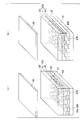
- (A) is a perspective view in case a dielectric film has a hole part
- (b) is a perspective view in case a dielectric film has an island-shaped part.
- the cathode portion is shown apart.
- (A) is a perspective view in case a dielectric film and an anode have a hole part
- (b) is a perspective view in case a dielectric film and an anode have an island-shaped part.
- the cathode portion is shown apart. It is a cross-sectional schematic diagram for demonstrating the organic EL element which concerns on the 4th Embodiment of this invention. It is a perspective view for demonstrating an example of the organic EL element which concerns on the 4th Embodiment of this invention.
- (A) is a perspective view in case an anode has a hole part
- (b) is a perspective view in case an anode has a convex part.
- the cathode portion is shown apart. It is a cross-sectional schematic diagram for demonstrating the organic EL element which concerns on the 5th Embodiment of this invention.
- FIG. 1 It is a perspective view for demonstrating an example of the organic EL element which concerns on the 5th Embodiment of this invention.
- (A) is a perspective view in case an anode has a hole part
- (b) is a perspective view in case an anode has a convex part. In order to clearly show the features of the invention, the cathode portion is shown apart.
- (A) is a perspective view in case an anode has a hole part
- (b) is a perspective view in case an anode has a convex part.
- the cathode portion is shown apart.
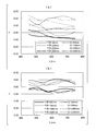
- (A) shows the result when the distance from the light emitting point to the reflective layer is 50 to 300 nm
- (b) shows the result when the distance from the light emitting point to the reflective layer is 500 to 1500 nm.
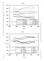
- (A) shows the result when the distance from the light emitting point to the reflective layer is 50 to 300 nm
- (b) shows the result when the distance from the light emitting point to the reflective layer is 500 to 1500 nm.
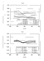
- (A) shows the result when the distance from the light emitting point to the reflective layer is 50 to 300 nm
- (b) shows the result when the distance from the light emitting point to the reflective layer is 500 to 1500 nm.
- (A) shows the result when the distance from the light emitting point to the reflective layer is 50 to 300 nm
- (b) shows the result when the distance from the light emitting point to the reflective layer is 500 to 1500 nm.
- the organic EL device includes a pair of electrodes facing each other and an organic layer including a light emitting layer provided between the pair of electrodes, and one of the pair of electrodes is a metal electrode.
- the other electrode is a translucent electrode, and an organic layer such as a charge injection layer, a charge transport layer, or a charge block layer is provided on the light emitting layer side of the metal electrode.
- the configuration of the bottom emission type will be described, but the organic EL element according to the present invention may be a top emission type.
- the first electrode is an anode and the second electrode is a cathode
- a configuration in which the first electrode is a cathode and the second electrode is an anode may be used.
- the organic EL device of the present invention may include a layer not described below as long as the effects of the present invention are not impaired.
- light propagating in the organic layer at a relatively large propagation angle may be simply referred to as guided mode light.
- the organic EL device comprises a first electrode, an organic layer including a light emitting layer, and a second electrode in this order on a substrate, and one of the first electrode and the second electrode is a transparent electrode.
- the other is a metal electrode.
- This organic EL element includes a dielectric layer on at least a part of the organic layer and / or the first electrode and / or the substrate.
- the dielectric layer and the organic layer and / or the first electrode and / or the substrate form a plurality of island-shaped portions, at least one of which has a regular shape, and at least a portion of the other is the island-shaped portion.
- a sea-like portion is continuously formed so as to fill the periphery of the sea, and they are formed so as to form a sea-island structure.
- the organic layer includes an organic thick film layer having a thickness of 80 nm to 1500 nm between the light emitting layer and the metal electrode.
- the organic EL device is intended to suppress the generation of SPP mode light itself and improve the light extraction efficiency by effectively extracting SPP mode light and waveguide mode light.
- an organic thick film layer having a thickness of 80 nm or more and 1500 nm or less is formed between the light emitting layer and the metal electrode.
- the distance between the light emitting position and the metal electrode can be increased to suppress energy transfer to the metal electrode.
- production of SPP mode light itself can be reduced.
- a dielectric layer is provided on at least a part of the organic layer and / or the first electrode and / or the substrate on the light extraction side, and the dielectric layer and the organic layer and / or The first electrode and / or the substrate form a plurality of island-shaped portions, at least one of which has a regular shape, and is continuously sea-shaped so that at least a portion of the other fills the periphery of the island-shaped portion.
- the guided mode light can be refracted in a direction perpendicular to the substrate surface by the refractive index profile of the sea-island structure.
- the organic EL device according to the present invention exhibits any one of the effect of refracting the above-described guided mode light in a direction nearly perpendicular to the substrate, the effect of diffraction, and the effect of a photonic crystal.
- the first electrode and the organic layer or the substrate continuously form a plurality of islands having at least one part of which has a regular shape, and at least a part of the other part fills the periphery of the island part.
- the shaped portions they can also form a sea-island structure.
- any one of the effect of refracting the guided mode light in a direction perpendicular to the substrate, the effect of diffraction, and the effect of the photonic crystal is achieved by the refractive index distribution shape of the sea-island structure.
- the organic EL device according to the present invention will be described with a specific example of a sea-island structure.
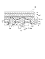
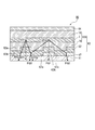
- FIG. 1 is a schematic cross-sectional view for explaining an example of the organic EL element according to the first embodiment of the present invention.
- the organic EL element 10 according to the first embodiment includes, on a substrate 11, an anode 12, an organic layer 13 including a light emitting layer 3 made of an organic EL material, and a cathode 14 in this order. Between the anode 12 and the cathode 14, a dielectric layer 17 having a refractive index different from the refractive index of the organic layer 13 and having a plurality of holes 17A (see FIG. 18F) is provided. .
- the organic layer 13 includes an organic thick film layer 18 having a thickness of 80 nm or more and 1500 nm or less between the light emitting layer 3 and the cathode 14, and the organic layer 13 further includes an inner surface 17a of the hole 17A. Has a hole inner surface covering portion 13a.
- the anode 12 includes an anode hole portion 12A (see FIG. 18 (h)) communicating with the hole portion 17, and the substrate 11 has a recess 11A (see FIG. 18 (h)) communicating with the anode hole portion 12A. Is provided.
- the organic layer 13 further includes a hole inner surface covering portion 13a covering the inner surface 17a of the hole 17A, an anode hole inner surface covering portion 13b covering the inner surface 12a of the anode hole 12A, and the recess 11A. And a recess inner side surface covering portion 13c that covers the inner side surface 11a.
- the hole inner surface covering portion, the anode hole inner surface covering portion, and the recess inner surface covering portion may be constituted by a part of the layers constituting the organic layer.
- the dielectric layer 17, the anode 12, and the substrate 11 form a sea-like portion.
- the communicating hole 17A, anode hole 12A, hole inner side surface covering part 13a covering the concave part 11A, anode hole inner side surface covering part 13b, and concave inner side surface covering part 13c form an island-shaped part.
- the sea-island structure does not reverse. This is because when the anode 12 becomes an island-shaped portion, it is impossible to obtain mutual conduction.
- the organic layer 13 further includes a dielectric layer 17 and a layered portion 13 d disposed between the hole inner surface covering portion 13 a and the cathode 14.
- the layered portion 13 d includes the light emitting layer 3 and the organic thick film layer 18.
- the organic layer 13 shown in FIG. 1 further includes an organic layer having a function of transporting at least holes, such as a hole transport layer and a hole injection layer, closer to the anode side than the light emitting layer 3.
- the hole 17A, anode hole 12A and recess 11A are arranged in at least one direction within the substrate surface is equal to or greater than the wavelength of the emitted light
- the hole 17A, anode hole 12A and recess The shape of 11A is not particularly limited as long as it has an effect of refracting light toward the substrate side on the inner surface thereof. From the viewpoint of refracting the guided mode light to the substrate 11 side, the angle formed by the inner surface 17a of the hole 17A and the substrate surface is preferably close to vertical. In the example shown in FIG. 1, the inner side surface 17 a of the hole 17 ⁇ / b> A is arranged substantially perpendicular to the substrate surface.
- the angle formed by the inner surface 17a of the hole 17A and the bottom surface on the substrate side is preferably 45 ° to 135 °, more preferably 60 ° to 120 °, and even more preferably 75 ° to 105 °. preferable.
- the shape of the hole, anode hole, and recess has diffraction effects and photonics. There is no particular limitation as long as the effect of the crystal is exhibited. From the viewpoint of extracting emitted light to the substrate side, the inner surfaces of the hole portion 17A, the anode hole portion 12A, and the recess portion 11A are formed on the substrate regardless of the refractive index relationship between the hole inner surface covering portion 13a and the dielectric layer 17. It is preferable that the surface is nearly perpendicular to the surface.
- the refractive index modulation becomes steep in the in-plane direction of the substrate across the side surface of the hole 17A because the inner surfaces of the hole, anode hole, and recess are substantially perpendicular to the substrate surface.
- the refractive index modulation is steep, the photonic crystal has a wider band gap frequency range in which light cannot propagate in the in-plane direction of the substrate, and can be extracted from the organic layer 13 to the outside more efficiently. Even in the diffraction grating, the diffraction efficiency of light toward the substrate is improved, so that the extraction of light to the outside of the element is also improved.
- the organic EL element of the present invention can be applied only to a bottom emission type organic EL element because the substrate has an uneven shape.
- the substrate 11 is a light-transmitting substrate and usually needs to be transparent to visible light.
- transparent to visible light means that it is only necessary to transmit visible light having a wavelength emitted from the light emitting layer, and does not need to be transparent over the entire visible light region.
- a smooth substrate having a transmittance in visible light of 400 to 700 nm of 50% or more is preferable. More preferably, the transmittance is 70% or more.
- a glass plate, a polymer plate, etc. are mentioned.
- the glass plate include soda lime glass, barium / strontium-containing glass, lead glass, aluminosilicate glass, borosilicate glass, barium borosilicate glass, and quartz.
- the polymer plate include polycarbonate, acrylic, polyethylene terephthalate, polyethylene naphthalate, polyether sulfide, and polysulfone.
- the transmittance is preferably 50% or more and more preferably 70% or more with respect to the wavelength at which light emission has the maximum intensity.
- the thickness of the substrate 11 is not limited because it depends on the required mechanical strength, but is preferably 0.01 mm to 10 mm, more preferably 0.05 mm to 2 mm. However, in this embodiment, since the substrate 11 includes a plurality of recesses 11A, it is preferable that the material be easily processed more accurately. Although it does not limit as a preferable material, For example, quartz is mentioned.
- the anode 12 includes a plurality of anode holes 12A (see FIG. 18 (h)).
- the inner surface 12a of the anode hole 12A is covered with the organic layer 13 (the anode hole inner surface covering part 13b), and the upper surface of the anode 12 is covered with the dielectric layer 17.
- the anode hole 12A may be filled or may be partially filled.
- the anode 12 is an electrode for applying a voltage between the anode 14 and injecting holes into the organic layer 13 from the anode 12, and is made of a metal, an alloy, a conductive compound, or a mixture thereof having a high work function. It is preferable to use a material. It is preferable to use one having a work function of 4 eV or more and 6 eV or less so that the difference from the HOMO (Highest Occupied Molecular Orbital) level of the organic layer in contact with the anode does not become excessive.
- the material of the anode 12 is not particularly limited as long as it is a translucent and conductive material.
- conductive high conductivity doped with transparent inorganic oxides such as indium tin oxide (ITO), indium zinc oxide (IZO), tin oxide, zinc oxide, conductive polymers such as PEDOT: PSS, polyaniline, and arbitrary acceptors.
- transparent inorganic oxides such as indium tin oxide (ITO), indium zinc oxide (IZO), tin oxide, zinc oxide, conductive polymers such as PEDOT: PSS, polyaniline, and arbitrary acceptors.
- examples include molecules, conductive light-transmitting materials such as carbon nanotubes, thin film metals, metal nanowires formed into a thin film, and composite materials including these.
- the anode 12 can be formed on the substrate 11 by, for example, a sputtering method, a vacuum deposition method, a coating method, or the like.
- the thickness of the anode 12 is not particularly limited, but is, for example, 10 to 2000 nm, and preferably 50 to 1000 nm. When the anode 12 is thinner than 10 nm, the waveguide mode light is hardly scattered. If the thickness of the anode 12 is larger than 2000 nm, the flatness of the organic layer 13 cannot be maintained and the transmittance of the anode is lowered.
- the cathode 14 is an electrode for injecting electrons into the light emitting layer, and it is preferable to use a material made of a metal, an alloy, a conductive compound, or a mixture thereof having a small work function. It is preferable to use one having a work function of 1.9 eV or more and 5 eV or less so that the difference from the LUMO (Lowest Unoccupied Molecular Orbital) level of the organic layer in contact with the anode does not become excessive.
- LUMO Local Unoccupied Molecular Orbital
- any material can be used as the cathode 14 as long as it is a highly conductive metal.
- Examples thereof include sodium, sodium-potassium alloy, magnesium, lithium, aluminum, silver, and alloys thereof such as magnesium / silver alloy. , Aluminum / aluminum oxide, aluminum / lithium alloy, indium, rare earth metal, and the like.
- the thickness of the cathode 14 is not particularly limited, but is, for example, 30 nm to 1 ⁇ m, and preferably 50 to 500 nm. If the thickness of the cathode 14 is less than 30 nm, the sheet resistance increases and the driving voltage rises. When the thickness of the cathode 14 is greater than 1 ⁇ m, damage due to heat and radiation during film formation and mechanical damage due to film stress accumulate in the electrode and the organic layer.
- the organic layer 13 includes a light emitting layer 3 made of an organic EL material, and includes an organic thick film layer 18 having a thickness of 80 nm to 1500 nm between the light emitting layer 3 and the cathode 12.
- the thickness of the organic thick film layer 18 is less than 80 nm, the effect of suppressing the generation of SPP mode light is insufficient. If the thickness of the organic thick film layer 18 exceeds 1500 nm, it takes too much time for film formation, which is not preferable in terms of productivity. Further, it is preferably 100 nm or more and 500 nm or less, and more preferably 120 nm or more and 300 nm or less.
- the thickness of the organic thick film layer 18 is 500 nm or less, the relative ratio of the refractive index modulation structure on the anode side in the organic EL element is increased, so that the refractive index modulation structure functions functionally. This is because waveguide mode light can be extracted from the substrate. Furthermore, if the thickness of the organic thick film layer 18 is 300 nm or less, an increase in driving voltage can be suppressed.
- the organic layer 13 may include a hole injection layer, a hole transport layer, an electron injection layer, and an electron transport layer in addition to a light emitting layer (organic light emitting layer) made of an organic EL material.
- the hole injection layer is a layer that assists hole injection from the anode 12 to the organic layer 13, and its ionization energy is usually as small as 5.5 eV or less.
- a material that injects holes into the organic layer 13 with a lower electric field strength is preferable. Any one can be selected and used.
- the hole transport layer is a layer that transports holes to the light emitting region and has a high hole mobility.
- the material to be formed as such a hole transport layer is not particularly limited as long as it can perform the above function, and any material can be selected and used from known materials.
- the electron injection layer is a layer that assists electron injection from the cathode 14 to the organic layer 13.
- a material that injects electrons into the organic layer 13 with a lower electric field strength is preferable.
- a material for forming these is not particularly limited as long as it can perform the above function, and is known in the art. Any one can be selected and used.
- the hole transport layer is a layer that transports holes to the light emitting region and has a high hole mobility.
- the material to be formed as such a hole transport layer is not particularly limited as long as it can perform the above function, and any material can be selected and used from known materials.
- the organic thick film layer 18 is a layer thickened to effectively suppress energy transfer between the light emitting position and the cathode, and there is no particular limitation on the material as long as it has a property of transporting at least electrons. .
- the organic thick film layer 18 may be an electron injection layer, an electron transport layer, a hole blocking layer, or a plurality of layers including them.
- the electron injection layer is generally a layer having a function of improving the electron injection efficiency from the cathode and having an effect of lowering the driving voltage of the element.
- the electron transport layer is a layer having a function of efficiently transporting electrons, and may have a function of suppressing the movement of holes.
- the layer 19 shown in FIG. 1 may be a hole injection layer, a hole transport layer, an electron block layer, or a plurality of layers including them.
- the organic layer 13 may include a layer made of another organic material.
- the anode is a light-transmitting material and the cathode is a metal material.
- the organic EL device according to the present invention may be configured such that the cathode is a light-transmitting material and the anode is a metal material.
- the thick film layer (arranged between the layer containing the light emitting material and the anode) is not particularly limited as long as it is a layer that transports holes, but the hole injection layer, the hole transport layer, the electronic block, Any of the layers may be included. Between the light emitting layer and the cathode, a layer including any of an electron injection layer, an electron transport layer, and a hole block layer may be provided.
- the film thickness of the organic thick film layer 18 is d, and the mobility is ⁇ .
- ⁇ i is a mobility with respect to electrons.
- ⁇ indicates that when the organic thick film layer is composed of a plurality of sublayers, the sum of d i 2 / ⁇ i of each sub layer is taken.
- the organic thick film layer is a single layer, the value of ⁇ is d 2 / ⁇ .
- the organic thick film layer is not so conductive, there is a problem that the drive voltage increases when the organic thick film layer is thick. Therefore, it is preferable to use a material with high mobility in order to suppress an increase in driving voltage even when the organic thick film layer is thickened.
- d 2 / ⁇ (d is the film thickness, ⁇ is the mobility) can be adopted as an index for considering the drive voltage, which corresponds to the resistance of the organic thick film layer.
- the organic thick film layer is preferably within the range of the above formula. If it is 10 ⁇ 15 [s ⁇ V] or more, SPP suppression is possible. When it is 10 ⁇ 4 [s ⁇ V] or less, it is possible to suppress an increase in drive voltage. In order to further improve the SPP suppression effect, it is preferably 10 ⁇ 11 [s ⁇ V] or more, more preferably 10 ⁇ 7 [s ⁇ V] or more, and further preferably 10 ⁇ 5 [s ⁇ V] or less. Good.
- the current density j in the layer i in the space charge limited current region is as follows: expressed.
- the unit is SI unit system.
- the voltage value of Equation (4) is preferably 1.0 V or less, more preferably 0.5 V or less, and 0.3 V More preferably, it is as follows.
- the value of the current density j 0.1 mA / cm 2 can be used as a typical value usually used in driving the organic EL element.
- the organic EL element of the example shown in FIG. 1 is a bottom emission type organic EL element.
- a configuration in which the electrode on the substrate side (anode in this example) is a transparent electrode and the other electrode (cathode in this example) is a metal electrode as viewed from the organic layer 13 is a typical embodiment.
- the layer 18 functions as an organic thick film layer.
- the organic layer 13 may be formed by a dry process such as an evaporation method or a transfer method, or may be formed by a wet process such as a spin coating method, a spray coating method, a die coating method, or a gravure printing method.
- the thickness of the organic layer 13 is not particularly limited, but is, for example, 50 to 2000 nm, and preferably 100 to 1000 nm. If the thickness of the organic layer 13 is less than 50 nm, quenching other than SPP coupling by metal occurs, such as a decrease in internal QE due to punch-through current and lossy surface wave mode coupling by the cathode 14. When the layer thickness of the organic layer 13 is greater than 1000 nm, the drive voltage increases.
- the organic thick film layer 18 has a thickness of 80 nm or more, and the distance between the light emitting layer 3 and the cathode 14 is large. The generation of SPP mode light at the interface between the cathode 14 and the thick film layer 18 itself is suppressed.
- the way of light propagation indicated by arrows in FIG. 1 is schematically shown in order to easily understand the principle of the refraction effect.
- the principle differs depending on the magnitude relationship between the refractive index of the dielectric layer 17 and the refractive index of the hole inner side surface covering portion 13a of the organic layer.
- the light propagation when the former is lower than the refractive index of the latter is represented by AP, and the light propagation when the former is higher than the refractive index of the latter is represented by AQ.
- the refraction at the inner surface is particularly exaggerated, but it goes without saying that refraction occurs at other interfaces in accordance with the law of refraction. The same applies to the arrows in the other drawings below.
- refraction occurs at the interface of materials having different refractive indexes, the refraction action is not shown in the drawing for the interface that is not particularly necessary for explaining the effect of the present invention.
- the vicinity of the shortest distance between the cathode 14 and the anode 12 has the highest current density and the amount of light emission increases.
- the light emission at the AP point and the AQ point of the light emitting layer included in the organic layer 13 schematically shows the light emission at the point where the light emission amount is large.
- the light AP2 is refracted at the interface between the dielectric layer 17 and the hole inner surface covering portion 13a (the inner surface 17a of the hole 17A), passes through the organic layer 13, and is refracted at the interface between the dielectric layer 17 and the substrate 11. Thus, it can be taken out through the substrate 11.
- the light AP2 travels from the hole inner surface covering portion 13a to the dielectric layer 17, the light AP2 is refracted at the interface between the dielectric layer 17 and the hole inner surface covering portion 13a (the inner surface 17a of the hole 17A).
- the incident angle from the organic layer 13 to the substrate 11 and the incident angle from the substrate 11 to the air are changed to small angles.
- Light incident on the interface between the organic layer 13 and the substrate 11 or the interface between the anode 12 and the substrate 11 at an angle greater than the critical angle is totally reflected to be guided mode light, but the light AP2 is the inner surface of the hole 17A.
- the incident angle from the organic layer 13 to the substrate 11 is changed to a small angle by refraction at 17a.
- the light AP2 is prevented from becoming waveguide mode light.
- Light incident on the outer surface of the substrate (for example, glass) at an angle greater than the critical angle is totally reflected and becomes substrate mode light.
- Light from the substrate 11 to the air is refracted at the inner surface 17a of the hole 17A. Since the incident angle of AP2 changes to a smaller angle, the light that is not totally reflected on the outer surface of the substrate increases, and the light extraction efficiency is improved. The same effect can be obtained for the light AP3.
- the light traveling through the organic layer 13 from the AP point is an interface between the concave inner surface covering portion 13c and the substrate 11 (the inner surface 11a of the concave portion 11A (extending perpendicular to the substrate 11).
- the refraction changes the angle of incidence on the substrate 11.
- the organic layer 13 and the substrate 11, and the substrate 11 and the air The light that can avoid total reflection at the interface increases the light extraction efficiency.
- the light AQ1 is the same as AP1.
- the interface between the dielectric layer 17 and the hole inner surface covering portion 13a (the inner surface 17a of the hole 17A). Due to the refraction at, the incident angle from the organic layer 13 to the substrate 11 and the incident angle from the substrate 11 to air change to small angles. Thereby, the light which can avoid the total reflection in the interface of a board
- the anode holes are periodically arranged, whereby the anode 12 (the dielectric layer 17 or the convex portion 11B of the substrate) and the anode hole inner side surface 12a.
- the organic layer 13a covering the substrate forms a diffraction grating
- the function and effect of the diffraction grating will be schematically described with reference to FIG.
- the way of propagation of light indicated by arrows in FIG. 2A is schematically shown in order to easily understand the principle of the effect of the diffraction grating.
- the principle described below does not depend on the magnitude relationship between the refractive indexes of the dielectric layer 17 and the hole inner surface covering portion 13a.
- the light emitted from the AP point of the light emitting layer included in the organic layer 13 propagates through the organic layer and enters the diffraction grating.
- the incident light is radiated by the diffraction grating in a predetermined direction (a direction satisfying the strengthening condition).
- the diffracted light is emitted at a certain predetermined angle because the diffracted light at each diffraction point is emitted while interfering.
- the arrow APD1 and the arrow APD2 light incident on the interface between the substrate 11 (for example, glass) and the outside (for example, air) at an incident angle equal to or less than the critical angle is directly extracted to the outside. Since the light indicated by the arrows APD1 and APD2 is intensified compared to other propagation directions due to interference as described above, it is possible to extract light having a high intensity at a specific angle, and the light extraction efficiency is improved. improves.
- the communicating hole portion 17A, anode hole portion 12A, and concave portion 11A have a period equal to or less than the wavelength of the emitted light in at least one direction in the plane of the substrate 11. If it is periodically arranged, it can be considered that the diffraction grating is formed as described above, and on the other hand, it can be regarded that the photonic crystal is formed.
- the effect by the photonic crystal will be schematically described with reference to FIG.
- the way of light propagation indicated by arrows in FIG. 2B is schematically shown in order to easily understand the principle of the effect of the photonic crystal.
- the principle described below does not depend on the magnitude relationship between the refractive indexes of the dielectric layer 17 and the hole inner surface covering portion 13a.
- the periodic structure includes a laminate of a dielectric layer 17, an anode 12, and a substrate convex portion 11B and an organic layer (a hole inner surface covering portion 13a, an anode hole inner surface covering portion 13b, and a recess inner surface covering portion. 13c).
- the photonic band gap can be generated in the direction of the arrow APP2 parallel to the substrate. Therefore, propagation in a direction parallel to the substrate is prohibited for light in the band gap frequency region corresponding to the APP2 direction.
- the photonic band gap does not occur in the direction perpendicular to the substrate because the periodic structure forming the photonic crystal is not formed. Therefore, the SPP mode light extracted as propagating light in the organic layer 13 travels in a direction (APD1 direction) that is nearly perpendicular to the substrate.
- APD1 direction the direction that is nearly perpendicular to the substrate.
- the photonic crystal structure changes the light propagation direction in the organic layer to a direction that is nearly perpendicular to the substrate surface, so that total reflection is suppressed and the light extraction efficiency to the outside is improved.
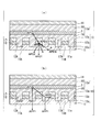
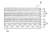
- FIG. 3 is a schematic cross-sectional view for explaining an example of the organic EL element according to the second embodiment of the present invention.
- the organic EL element according to the second embodiment may employ either a so-called bottom emission structure or a top emission structure.
- the organic EL element 20 according to the second embodiment of the present invention includes an anode 22, an organic layer 23 including a light emitting layer 3 made of an organic EL material, and a cathode 24 in this order.
- the organic layer 23 includes an organic thick film layer 18 having a thickness of 80 nm or more and 1500 nm or less between the light emitting layer 3 and the cathode 24.
- a dielectric layer 27 having a refractive index different from that of the organic layer 23 and having a plurality of hole portions 27A is provided.
- the organic layer 23 has a hole inner surface covering portion 23a that covers the inner surface 27a of the hole 27A.
- the organic layer 23 further includes a layered portion 23 d disposed between the dielectric layer 27 and the hole inner side surface hole inner surface covering portion 23 a and the cathode 24.
- the layered portion 23 d includes the light emitting layer 3 and the organic thick film layer 18.
- the hole inner surface hole inner surface covering section may be constituted by a part of the layers constituting the organic layer.
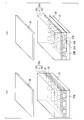
- FIG. 4A and 4B are perspective views for explaining an example of the organic EL element according to the second embodiment of the present invention.
- FIG. 4A shows an organic EL element in which the dielectric layer 27 forms a sea-like portion in plan view, and the hole inner side surface covering portion 23a forms an island-like portion.
- FIG. 4B shows an organic EL element in which the dielectric island-shaped outer surface covering portion 23s forms a sea-like portion and the dielectric layer island-like portion 27B forms an island-like portion in a plan view.
- the outer surface of the dielectric island 27B is the interface between the dielectric layer 27 and the hole inner surface hole inner surface covering portion 23a, like the inner surface of the hole 27A in FIG. 4A. This produces the effect of refracting light.
- the shape of the hole has the effect of refracting light toward the substrate on the inner surface. If it plays, there will be no limitation in particular.
- the inner surface 27a of the hole 27A and the substrate surface are independent of the refractive index relationship between the hole inner surface covering portion 23a and the dielectric layer 27. It is preferable that the angle formed by is close to vertical.
- the inner side surface is configured to be perpendicular to the substrate surface, but it is not necessary to have such a configuration.
- the angle formed by the inner side surface 27a of the hole 27A and the bottom surface of the hole 27A on the substrate 21 side, and the angle inside the hole 27A is preferably 45 ° to 135 °, more preferably 60 ° to 120 °, and more preferably 75 ° to 105 ° is even more preferable.
- the shape of the hole 27A is not particularly limited as long as the effect of diffraction and the effect of the photonic crystal are exhibited.
- the inner surface 27a of the hole 27A is perpendicular to the substrate surface regardless of the refractive index relationship between the hole inner surface covering portion 23a and the dielectric layer 27. It is preferable.
- the inner side surface 27a of the hole 27A is an interface that is perpendicular or nearly perpendicular to the substrate surface, so that the refractive index modulation is steep in the in-plane direction across the inner side surface 27a of the dielectric layer hole. It is to become.
- the refractive index modulation is steep, the frequency range of the photonic bandgap where light cannot propagate in the in-plane direction of the photonic crystal is widened, and the light emitted from the organic layer 23 is extracted more efficiently to the outside. Can do.
- Even in the diffraction grating since the diffraction efficiency of light to the substrate surface is improved, the extraction of light to the outside of the element is also improved. As described above, the same can be said regarding the shape of the hole 27A as the dielectric island 27B.
- the organic EL element of the present invention can be applied to any organic EL element of bottom emission type or top emission type.
- the same material and thickness of the substrate 21 as those of the substrate 11 of the first embodiment can be used.
- an opaque element can be used in addition to the same as described above.
- a substrate made of a simple metal, an alloy containing these, a material made of stainless steel, or the like, or a substrate normally used in other top emission type organic EL elements can be used.
- the organic layer 23 may be configured to fill the hole 27A or may be configured to partially fill.
- the convex outer surface covering portion is the outer surface 27b. If it covers, the structure which covers the whole surface of the dielectric island part 27B, or the structure which covers the one part may be sufficient.
- the refractive index of the organic layer refers to the refractive index of the hole inner surface covering portion 23a.
- the organic layer 23 includes a light emitting layer 3 made of an organic EL material, and includes an organic thick film layer 18 having a thickness of 80 nm or more and 1500 nm or less between the light emitting layer 3 and the cathode 22, and further includes a hole transport layer or a positive layer.
- the organic layer 23 includes a hole inner surface hole inner surface covering part 23a that covers the inner surface 27a of the hole 27A, and the dielectric layer 27 and the hole inner surface hole inner surface covering part 23a and the cathode 24. Has a layered portion 23b.
- the same materials as those in the first embodiment can be used.
- the effect of the organic EL element of this embodiment is typically demonstrated using FIG.
- the light propagation method indicated by the arrows in FIG. 3 is schematically shown in order to easily understand the principle of the effect.
- the organic thick film layer 18 has a thickness of 80 nm or more, and the distance between the light emitting layer 3 and the cathode 24 is large. It is difficult to move, and the generation of SPP mode light at the interface between the cathode 24 and the thick film layer 18 is suppressed.
- the light BP1 is perpendicular to the substrate among the light emitted at the BP point of the light emitting layer included in the organic layer 23. Light traveling in the direction toward the substrate side. Therefore, the light passes through the anode 22 and the substrate 21 without being refracted at the interface between the organic layer 23 and the anode 22 and the interface between the anode 22 and the substrate 21 and is taken out to the outside.
- the light BP2 is refracted toward the substrate 21 on the inner side surface 27a of the hole 27A, and can be extracted outside through the organic layer 23, the anode 22, and the substrate 21.
- total reflection may occur at the interface between the substrate 21 and the anode 22 and the outer surface of the substrate 21, but by having this interface (inner surface 27a), the inner surface of the hole 27A.
- Refraction at 27a changes the incident angle of the light propagating in the organic layer to the substrate 21 to a smaller angle. Therefore, light that is not totally reflected at the interface between the substrate 21 and the anode 22 and the outer surface of the substrate 21 increases, and the light extraction efficiency is improved.
- the light extraction efficiency is improved by having the configuration including the inner side surface 27a of the hole 27A.
- the light BP3 is refracted toward the substrate 21 on the inner side surface 27a of the hole 27A, so that it does not become waveguide mode light and substrate mode light, but passes through the organic layer 23, the anode 22, and the substrate 21 to the outside. Can be taken out.
- the light BQ1 is the same as BP1.
- BP2 and BP3 when light BQ2 and BQ3 travel from the dielectric layer 27 to the hole inner surface covering portion 23a, refraction at the interface between the dielectric layer 27 and the hole inner surface covering portion 23a causes the substrate from the organic layer 23.
- the incident angle to 21 and the incident angle from the substrate 21 to the air are changed to a small angle.
- the effects and operational effects of the photonic crystal are the same as those of the first embodiment, except that the diffraction grating and the photonic crystal are different.
- the diffraction grating and the photonic crystal are composed of the anode hole portion 12A, the hole portion 17A and the recess portion 11A, the hole inner surface covering portion 13a, the anode hole inner surface covering portion 13b, and the recess inner surface covering.
- the hole portion 27A and the hole inner surface covering portion 23a are composed of the anode hole portion 12A, the hole portion 17A and the recess portion 11A, the hole inner surface covering portion 13a, the anode hole inner surface covering portion 13b, and the recess inner surface covering.
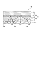
- FIG. 5 is a schematic cross-sectional view for explaining an example of the organic EL element according to the third embodiment of the present invention.
- the organic EL element according to the third embodiment may employ either a so-called bottom emission structure or a top emission structure.
- the organic EL element 30 according to the third embodiment of the present invention includes an anode 32, an organic layer 33 including the light emitting layer 3 made of an organic EL material, and a cathode 34 in this order.
- the organic layer 33 includes an organic thick film layer 18 having a thickness of 80 nm or more and 1500 nm or less between the light emitting layer 3 and the cathode 34.
- a dielectric layer 37 having a refractive index different from that of the organic layer 33 and having a plurality of holes 37A is provided between the anode 32 and the cathode 34.
- the organic layer 33 has a hole inner surface hole inner surface covering part 33a that covers the inner surface 37a of the hole 37A.
- the anode 32 includes an anode hole portion 32A communicating with the hole portion 37A.
- the organic layer further includes an anode hole inner surface hole inner surface covering portion 33b that covers the inner surface 32a of the anode hole 32A.
- the organic layer 33 further includes a layered portion 33 d disposed between the dielectric layer 37 and the hole inner surface hole inner surface covering portion 33 a and the cathode 34.
- the layered portion 33 c includes the light emitting layer 3 and the organic thick film layer 18.
- the organic layer 33 shown in FIG. 5 further includes an organic layer having a function of transporting at least holes, such as a hole transport layer and a hole injection layer, closer to the anode side than the light emitting layer 3.
- the hole inner surface covering portion 33a and the anode hole inner surface covering portion 33b may be constituted by a part of the layers constituting the organic layer.
- the organic EL element of the present invention can be applied to both a top emission type and a bottom emission type organic EL element as described above.
- the same materials as those of the substrate 21 of the second embodiment can be used for each of the top emission type and the bottom emission type.
- the anode 32 is provided with a plurality of anode holes 32A as in the first embodiment.
- the inner side surface 32 a of the anode hole portion 32 A is covered with the organic layer 33 (anode hole inner side surface hole inner surface side covering portion 33 b), and the upper surface thereof is covered with the dielectric layer 37.
- the anode hole inner surface hole inner surface covering portion 33b may be filled with the anode hole 32A or partially filled.
- the dielectric layer 37 has a refractive index lower than that of the organic layer and includes a plurality of holes 37A.
- the inner surface 37a of the hole 37A is covered with an organic layer 33 (hole inner surface hole inner surface covering portion 33a). As long as the inner surface 37a covers the inner surface 37a, the inner surface 37a of the hole may be filled with the hole 37A or may be partially filled.
- the organic layer 33 includes a light emitting layer 3 made of an organic EL material, and includes an organic thick film layer 18 having a thickness of 80 nm to 1500 nm between the light emitting layer 3 and the cathode 32, and a hole transport layer or hole An organic layer 19 having a function of transporting at least holes, such as an injection layer, is provided.
- the organic layer 33 includes a hole inner surface hole inner surface covering portion 33a that covers the inner surface 37a of the hole 37A, an anode hole inner surface hole inner surface covering portion 33b that covers the inner surface of the anode hole 32A, It has a layered portion 33d disposed between the dielectric layer 37 and the hole inner surface hole inner surface covering portion 33a and the cathode 34.
- FIGS. 6A and 6B are perspective views for explaining an example of the organic EL element according to the third embodiment of the present invention.
- FIG. 6A shows a case where the dielectric layer hole portion 37A and the anode hole portion 32A communicating with the dielectric layer hole portion 37A are arranged in plan view.
- FIG. 6B shows a dielectric island portion in which the anode convex portions 32B connected to each other are arranged in a protruding shape, and the same shape in a plan view on the anode convex portion pattern, and a dielectric film is formed in an island shape. This is the case with 37B.
- the dielectric layer 37 and the anode 32 form a sea-like portion, and the hole portion 37A and the hole inner surface covering portion 33a and the anode hole inner surface covering portion 33b covering the anode hole portion 32A are provided.
- the dielectric layer island-shaped portion 37B and the anode convex portion 32B form an island-shaped portion, and the dielectric island-shaped outer surface covering portion 33s and the anode convex outer surface covering portion 33t are sea-shaped portions. Is forming.
- the anode convex portion 32B in FIG. 6B is similar to the anode hole portion 32A in FIG. 6A in that light is transmitted at the interface between the anode 32A and the anode hole inner side surface hole inner surface side covering portion 33b. There is an effect of refracting in the direction closer to the line. Accordingly, not only FIG. 6A but also FIG. 6B in which the relationship between the laminate of the anode 32 and the dielectric film 37 and the sea island of the organic layer 33 is opposite to FIG. 6A can be used. .
- the shape of the hole portion 37A allows light to be transmitted on the inner surface thereof.
- the angle formed by the inner surface 37a of the hole 37A and the substrate surface is preferably close to perpendicular.
- the inner side surface 37 a of the hole 37 ⁇ / b> A is arranged substantially perpendicular to the substrate surface, but such a configuration is not necessary.
- the angle formed by the inner surface 37a of the hole 37A and the substrate surface, and the angle inside the hole 37A is preferably 45 ° to 135 °, more preferably 60 ° to 120 °, and even more preferably 75 ° to 105 °.
- the pitch between the adjacent hole portion 37A and the anode hole portion 32A is equal to or less than the wavelength of the emitted light
- the shape of the hole portion 37A and the anode hole portion 32A has the effect of diffraction and the effect of the photonic crystal. If it is a thing, there will be no limitation in particular.
- the inner surfaces of the hole and the anode hole are substantially perpendicular to the substrate surface. This is because the refractive index modulation becomes steep in the in-plane direction of the substrate crossing the side surface of the hole 37A because the inner surfaces of the hole and the anode hole are substantially perpendicular to the substrate surface.
- the photonic crystal When the refractive index is sharply modulated, the photonic crystal has a wider photonic band gap frequency range where light cannot propagate in the in-plane direction of the substrate, and can be extracted from the organic layer 33 to the outside more efficiently. Even in the diffraction grating, the diffraction efficiency of light toward the substrate is improved, so that the extraction of light to the outside of the element is also improved. As described above, the same can be said with respect to the shape even when the hole and anode hole are formed as dielectric island portions and anode protrusions.
- the same materials as those in the first embodiment can be used.
- the effect of the organic EL element of this embodiment is typically demonstrated using FIG.
- the light propagation method indicated by the arrows in FIG. 5 is schematically shown in order to easily understand the principle of the effect.
- the organic thick film layer 18 has a thickness of 80 nm or more, and the distance between the light emitting layer 3 and the cathode 34 is large, so that the energy transfer is difficult and the SPP mode light Occurrence itself is suppressed.
- the current density is highest near the shortest distance between the cathode 34 and the anode 32, and the amount of light emission is increased.
- the light emission at the CP and CQ points of the light emitting layer included in the organic layer 33 schematically shows the light emission at the point where the light emission amount is large.
- the refractive index of the hole inner surface hole inner surface covering portion 33a of the organic layer is higher than the refractive index of the dielectric layer 37
- the light CP1 of the light emitted at the CP point of the light emitting layer included in the organic layer 33 is the substrate.
- the light travels in the direction perpendicular to the substrate side, travels through the substrate 31 without being refracted at the interface between the organic layer 33 and the substrate 31, and is extracted outside.
- the light CP2 is refracted toward the substrate 31 at the inner side surface 37a of the hole 37A, passes through the dielectric layer 37, refracts at the interface between the dielectric layer 37 and the anode 32, travels through the anode 32, and After being refracted at the interface with the substrate 31, it can be taken out through the substrate 31.
- the refraction at the interface between the organic layer 33 and the dielectric layer 37 causes a more incident angle to the substrate 31. Change to a small angle.
- the light CQ1 is the same as CP1.
- the light beams CQ2 and CQ3 travel from the dielectric layer 37 to the hole inner surface hole inner surface covering portion 33a due to refraction at the interface between the dielectric layer 37 and the hole inner surface hole inner surface covering portion 33a.
- the incident angle from the organic layer 33 to the substrate 31 and the incident angle from the substrate 31 to the air are changed to small angles. Thereby, the light which can avoid the total reflection in the interface of a board
- the communicating hole portion 37A and anode hole portion 32A are periodically arranged in at least one direction within the surface of the substrate 31 with a period equal to or less than the wavelength of the emitted light.
- the operation effect by the diffraction grating and the operation effect by the photonic crystal are the same as those of the first embodiment except that the diffraction grating and the photonic crystal are different.
- the diffraction grating and the photonic crystal are composed of the anode hole portion 12A, the hole portion 17A, the recess portion 11A, the hole inner surface covering portion 13a, the anode hole inner surface covering portion 13b, and the recess inner surface covering.
- the anode hole portion 32A, the hole portion 37A, the anode hole inner surface covering portion 33b, and the hole inner surface covering portion 33a are composed of the anode hole portion 12A, the hole portion 17A, the recess portion 11A, the hole inner surface covering portion 13a, the anode hole inner surface covering portion 13b,
- FIG. 7 is a schematic cross-sectional view for explaining an example of the organic EL element according to the fourth embodiment of the present invention.
- the organic EL element according to the fourth embodiment may employ either a so-called bottom emission structure or a top emission structure.
- the organic EL element 40 according to the fourth embodiment of the present invention includes an anode 42, an organic layer 43 including the light emitting layer 3 made of an organic EL material, and a cathode 44 in this order.
- the organic layer 43 includes an organic thick film layer 18 having a thickness of 80 nm or more and 1500 nm or less between the light emitting layer 3 and the cathode 44.
- the anode 42 includes a plurality of anode hole portions 42A (see FIG. 21E) whose inner side surface 42a is covered with a dielectric layer 47 having a refractive index different from the refractive index of the anode 42.
- FIG. 8A and 8B are perspective views for explaining an example of the organic EL element according to the fourth embodiment of the present invention.
- FIG. 8A shows the case where the anode holes are arranged in plan view.
- FIG. 8B is a perspective view for explaining another example of the organic EL element in which the anode convex portions 42B connected to each other are arranged in a protruding shape.
- the anode 42 forms a sea portion and the dielectric layer 47 forms an island portion.
- the dielectric layer 47 forms a sea portion and the anode 42 forms an island portion.
- the anode convex portion 42B has an effect of refracting light incident from the organic layer 43 side in a direction closer to the normal line of the substrate 41.
- the anode convex portion 42B has an effect of refracting light toward the substrate side at the interface between the dielectric layer 47 and the anode 42b, similarly to the anode hole portion 42A in FIG. Therefore, FIG. 8A and FIG.
- the shape of the anode hole portion refracts light toward the substrate side on the inner surface thereof. If there is an effect, there is no limitation in particular. From the viewpoint of refracting the guided mode light more vertically, it is preferable that the angle formed by the inner surface 42a of the anode hole portion 42A and the substrate surface is close to the vertical. In the example shown in FIG. 7, the inner side surface is configured to be perpendicular to the substrate surface, but is not limited to this configuration. The angle of the inner side surface 42a of the anode hole portion 42A with respect to the substrate surface is preferably 45 to 135, more preferably 60 to 120 °, and even more preferably 75 to 105 °.
- the shape of the anode hole portion 42A has a diffraction effect or a photonic crystal effect.
- the inner surfaces of the hole and the anode hole are substantially perpendicular to the substrate surface. This is because the modulation of the refractive index becomes steep in the in-plane direction of the substrate across the side surface of the anode hole 42A because the inner surface of the anode hole 42A is substantially perpendicular to the substrate surface.
- the photonic crystal When the refractive index is sharply modulated, the photonic crystal has a wider band gap frequency range where light cannot propagate in the in-plane direction of the substrate, and can be extracted from the organic layer 43 to the outside more efficiently.
- the diffraction efficiency of the light toward the substrate is improved even in the diffraction grating, the light extraction to the outside of the element is similarly improved. As described above, the same can be said with respect to the shape even when the anode hole portion is an anode convex portion.
- the organic EL element of the present invention can be applied to both a top emission type and a bottom emission type organic EL element as described above.
- the same material as the substrate 21 of the second embodiment can be used for each of the top emission type and the bottom emission type.
- the same materials as those in the first embodiment can be used.
- the anode 42 includes a plurality of anode holes 42A (see FIG. 21 (e)).
- the inner side surface 42a of the anode hole 42A is covered with a dielectric layer 47 having a refractive index lower than that of the anode 42.
- the dielectric layer 47 covers the inner side surface 42a, the anode layer 42A may be filled or may be partially filled.
- the dielectric layer 47 covers the inner side surface 42a of the anode hole 42A of the anode 42 and is made of a material having a refractive index lower than that of the anode 42.
- the dielectric layer 47 has such a configuration and material because the light incident on the inner side surface 42a of the anode hole portion 42A is refracted toward the substrate 41 at this interface so that the incident angle of the waveguide mode light is reduced to a small angle. This is for changing the ratio of light that causes total reflection and improving light extraction efficiency.
- the organic layer 43 includes the light emitting layer 3 made of an organic EL material, and includes the organic thick film layer 18 having a film thickness of 80 nm or more and 1500 nm or less between the light emitting layer 3 and the cathode 42.
- the organic layer 43 shown in FIG. 7 further includes an organic layer 19 having a function of transporting at least holes, such as a hole transport layer and a hole injection layer, closer to the anode side than the light emitting layer 3.
- the effect of the organic EL element of this embodiment is typically demonstrated using FIG.
- the light propagation method indicated by the arrows in FIG. 7 is schematically shown for easy understanding of the principle of the effect.
- the organic thick film layer 18 has a thickness of 80 nm or more, and the distance between the light emitting layer 3 and the cathode 44 is large. The generation of light itself is suppressed.
- the light DP1 is light that travels perpendicular to the substrate toward the substrate. Yes, it proceeds through the substrate 41 without being refracted at the interface with the substrate 41 and is taken out to the outside.
- the light DP2 is refracted at the inner side surface 42a of the anode hole portion 42A (the interface between the anode 42 and the dielectric layer 47 extending perpendicularly to the substrate surface of the substrate 41), passes through the dielectric layer 47, and passes through the dielectric.
- the incident angle on the substrate 41 changes to a smaller angle due to refraction at the inner side surface 42a of the anode hole 42A.
- the incident angle on the substrate 41 is changed to a smaller angle by refraction at the inner surface 42a. Therefore, the light that is not totally reflected on the outer surface of the substrate increases, and the light extraction efficiency is improved. The same effect can be obtained for the light CR3.
- the light DQ1 is the same as DP1.
- DP2 and DP3 when the light DQ2 and DQ3 travel from the dielectric 47 to the anode 42, refraction at the interface between the anode 42 and the dielectric 47 causes the incident angle from the organic layer 43 to the substrate 41 and the outside of the substrate 41. The angle of incidence on the surface changes to a smaller angle. Thereby, the light which is not totally reflected on the outer surface of the substrate increases, and the light extraction efficiency is improved.
- the anode hole portion 42A is formed by a diffraction grating that is generated by being periodically arranged in at least one direction in the plane of the anode 42 with a period equal to or less than the wavelength of the emitted light.
- the operation effect and the operation effect by the photonic crystal are the same as those of the first embodiment except that the diffraction grating and the photonic crystal are different.
- the diffraction grating and the photonic crystal are composed of the anode hole portion 12A, the hole portion 17A and the recess portion 11A, the hole inner surface covering portion 13a, the anode hole inner surface covering portion 13b, and the recess inner surface covering.
- the anode 42 and the dielectric layer 47 are composed of the anode hole portion 12A, the hole portion 17A and the recess portion 11A, the hole inner surface covering portion 13a, the anode hole inner surface covering portion 13b, and the recess inner surface covering.
- FIG. 9 is a schematic cross-sectional view for explaining an example of the organic EL element according to the fifth embodiment of the present invention.
- the organic EL element according to the fifth embodiment may employ either a so-called bottom emission structure or a top emission structure.
- An organic EL element 50 according to the fifth embodiment of the present invention includes an anode 52, an organic layer 53 including a light emitting layer made of an organic EL material, and a cathode 54 in this order.
- the organic layer 53 includes an organic thick film layer 18 having a thickness of 80 nm or more and 1500 nm or less between the light emitting layer 3 and the cathode 54.
- the anode 52 includes a plurality of anode holes 52A (see FIG.
- the organic layer 53 includes an anode hole inner surface hole inner surface covering part 53a covering the inner surface 52a of the anode hole 52A, the anode 52 and the anode hole inner surface hole inner surface covering part 53a, and the cathode 54. And a layered portion 53b disposed between the two.
- the organic layer 53 shown in FIG. 9 includes the organic layer 19 having a function of transporting at least holes, such as a hole transport layer and a hole injection layer, on the anode side from the light emitting layer 3.
- FIGS. 10A and 10B are perspective views for explaining an example of the organic EL element according to the fifth embodiment of the present invention.
- FIG. 10A shows an organic EL element in which anode holes are arranged in a plan view.
- FIG. 10B shows an organic EL element in which anode projections 52B connected to each other are arranged in a protruding shape. That is, in FIG. 10A, the anode 52 forms a sea portion, and the anode hole inner side surface hole inner surface covering portion 53a forms an island portion. In FIG. 10B, the anode convex portion 52B forms an island-shaped portion, and the dielectric island-shaped outer surface covering portion 53s forms a sea-shaped portion.
- FIG. 10A and FIG. 10B in which the relationship between the anode and the sea-island structure of the organic layer are reversed can be used.
- the shape of anode hole portion 52A has the effect of refracting light toward the substrate side on the inner side surface. If it plays, there will be no limitation in particular. From the viewpoint of refracting the guided mode light toward the substrate 51, the angle formed by the inner surface 52a of the anode hole portion 52A and the substrate surface is preferably close to vertical. In the example shown in FIG. 9, the inner side surface 52a of the anode hole 52A is arranged substantially perpendicularly to the substrate surface, but such a configuration is not necessary.
- the angle between the inner surface 52a of the anode hole 52A and the substrate surface, and the angle inside the anode hole 52A is preferably 45 ° to 135 °, more preferably 60 ° to 120 °, and even more preferably 75 ° to 105 °. preferable.
- the shape of anode hole portion 52A can exhibit the effect of diffraction or the effect of photonic crystals.
- the inner surfaces of the hole and the anode hole are substantially perpendicular to the substrate surface. This is because the refractive index modulation becomes steep in the in-plane direction of the substrate crossing the side surface of the anode hole 52A because the inner surface of the anode hole is substantially perpendicular to the substrate surface.
- the photonic crystal When the refractive index is sharply modulated, the photonic crystal has a wider band gap frequency range where light cannot propagate in the in-plane direction of the substrate, and can be extracted from the organic layer 53 to the outside more efficiently. Even in the diffraction grating, since the diffraction efficiency of light in the direction perpendicular to the substrate surface is improved, the light extraction to the outside of the element is also improved. As described above, the same can be said with respect to the shape even when the anode hole portion is an anode convex portion.
- the organic EL element of the present invention can be applied to both a top emission type and a bottom emission type organic EL element as described above.
- the same material as the substrate 21 of the second embodiment can be used for each of the top emission type and the bottom emission type.
- the same materials as those in the first embodiment can be used.
- the effect of the organic EL element of this embodiment is typically demonstrated using FIG.
- the light propagation method indicated by the arrows in FIG. 9 is schematically shown in order to easily understand the principle of the effect.
- the organic thick film layer 18 has a thickness of 80 nm or more, and the distance between the light emitting layer 3 and the cathode 54 is large. The occurrence itself is suppressed.
- the light EP1 is light that travels perpendicularly to the substrate toward the substrate side among the light emitted at the EP point of the light emitting layer included in the organic layer 53. Further, the light passes through the anode 52 and the substrate 51 without being refracted at the interface between the organic layer 53 and the anode 52 and the interface between the anode 52 and the substrate 51, and is taken out to the outside.
- the light EP2 is refracted at the interface between the organic layer 53 and the anode 52, enters the anode 52, passes through the anode 52, and refracts at the interface between the anode 52 and the organic layer 53a (the inner side surface 52a of the anode hole 52A). Then, it can be taken out through the anode 52 and the substrate 51.
- the light EP2 is refracted toward the substrate 51 at the inner side surface 52a of the anode hole 52A, and can be extracted outside through the organic layer 53 and the substrate 51. In the configuration without this interface (inner side surface 52 a), total reflection may occur at the interface between the substrate 51 and the anode 52 or the organic layer 53 and the outer surface of the substrate 51.
- the incident angle of the light propagating in the organic layer to the substrate 51 changes to a smaller angle due to refraction at the inner side surface 52a of the anode hole 52A. For this reason, the amount of light that is not totally reflected increases, and the light extraction efficiency is improved. That is, the light extraction efficiency is improved by having the configuration including the inner side surface 52a of the anode hole 52A. Similar effects can be obtained with the light EP3.
- the light EQ1 is the same as the light EP1.
- the light EQ2 and the light EQ3 are incident on the interface between the organic layer 53 and the substrate 51 by refraction at the interface between the anode 52 and the organic layer 53 when traveling from the organic layer 53 to the anode 52.
- the incident angle to the outer surface of the substrate 51 changes to a small angle.
- the anode hole 52A is formed by a diffraction grating that is generated by periodically arranging the anode hole 52A in at least one direction in the plane of the substrate 51 with a period equal to or less than the wavelength of the emitted light.
- the operation effect and the operation effect by the photonic crystal are the same as those of the first embodiment except that the diffraction grating and the photonic crystal are different.
- the diffraction grating and the photonic crystal are composed of the anode hole portion 12A, the hole portion 17A, the recess portion 11A, the hole inner surface covering portion 13a, the anode hole inner surface covering portion 13b, and the recess inner surface covering.
- the anode 52 and the hole inner surface covering portion 53a are composed of the anode hole portion 12A, the hole portion 17A, the recess portion 11A, the hole inner surface covering portion 13a, the anode hole inner surface covering portion 13b, and the recess inner surface covering.
- FIG. 11 is a schematic cross-sectional view for explaining an example of the organic EL element according to the sixth embodiment of the present invention.
- the organic EL element according to the sixth embodiment may employ either a so-called bottom emission structure or a top emission structure.
- An organic EL element 60 according to the sixth embodiment of the present invention includes a dielectric layer 67, an anode 62, an organic layer 63 including a light emitting layer 3 made of an organic EL material, and a cathode 64 in this order.
- the organic layer 63 includes an organic thick film layer 18 having a thickness of 80 nm to 300 nm between the light emitting layer 3 and the cathode 64.
- the dielectric layer 67 has a refractive index different from that of the anode 62 and has a pattern having an opening 67A so that the substrate 61 is exposed. Both surfaces of the anode 62 and the surface of the organic layer 63 on the anode 62 side are formed so as to follow the pattern of the dielectric layer 67.
- the organic layer 63 shown in FIG. 11 further includes an organic layer 19 having a function of transporting at least holes, such as a hole transport layer and a hole injection layer, closer to the anode side than the light emitting layer 3.
- a planarizing film may be formed on the organic layer 63 side of the anode 62 that follows the pattern of the dielectric layer 67.
- the planarizing film is a film that planarizes the surface of the organic layer 63 on the anode 62 side, and is formed so as to fill the hole of the anode 62.
- planarizing film covers part of the surface of the anode 62, it may be transparent with visible light, whether or not it has conductivity, and the same material as the dielectric layer 67 and the anode 62 is used. be able to.
- the planarizing layer for example, a dry process method such as a resistance heating vapor deposition method, an electron beam vapor deposition method, a sputtering method, an ion plating method, a CVD method, or a wet process such as a coating method can be used. .
- FIG. 12 is a perspective view for explaining an example of the organic EL element according to the sixth embodiment of the present invention.
- the sea-island structure is formed in two places.
- the portion of the anode 62 filling the opening of the dielectric layer 67 forms an island-like portion separated from each other in plan view, and the dielectric layer 67 having the opening has the sea-like portion.
- the anode hole inner side surface covering portion 63a filling the anode hole 62A forms an island-like portion separated from each other in plan view, and the portion of the anode 62 having an opening has the sea-like portion.
- the sea-island structure is also formed in two places in FIG.
- the dielectric layer convex portion 67B forms an island-shaped portion
- the portion of the anode 62 that covers the dielectric layer convex portion 67B forms a sea-shaped portion.
- the anode convex portion 62B forms an island-shaped portion
- the anode convex portion outer surface covering portion that covers the anode convex portion 62B forms a sea-shaped portion.
- This anode convex portion 62B has an effect of refracting light toward the substrate, similarly to the anode hole portion 62A in FIG. Therefore, in order to obtain the same effect regardless of whether the dielectric 67 is a sea part or an island part of the sea-island structure, the following description will be made on the structure shown in FIG.
- the same materials as those in the first embodiment can be used.
- the shape of the openings of the dielectric layers 67 is such that light is transmitted on the inner surface thereof.
- the angle formed by the inner surface 67a of the opening 67A and the substrate surface is preferably close to vertical.
- the inner surface 67a of the opening 67A is arranged substantially perpendicular to the substrate surface, but it is not necessary to have such a configuration.
- the angle between the inner surface 67a of the hole 67A and the substrate surface, and the angle inside the hole 67A is preferably 45 ° to 135 °, more preferably 60 ° to 120 °, and even more preferably 75 ° to 105 °.
- the shape of the openings of the dielectric layers 67 has the effect of diffraction and the effect of photonic crystals. If it plays, there will be no limitation in particular.
- the inner surfaces of the hole and the anode hole are substantially perpendicular to the substrate surface. This is because the modulation of the refractive index becomes steep in the in-plane direction of the substrate across the side surface of the opening of the dielectric layer 67 because the inner surface of the hole and the anode hole is substantially perpendicular to the substrate surface. It is.
- the photonic crystal When the refractive index is sharply modulated, the photonic crystal has a wider band gap frequency range where light cannot propagate in the in-plane direction of the substrate, and can be extracted from the organic layer 63 to the outside more efficiently. Even in the diffraction grating, the diffraction efficiency of light toward the substrate is improved, so that the extraction of light to the outside of the element is also improved. As described above, the same can be said with respect to the shape even when the opening of the dielectric layer is a dielectric protrusion.
- FIG. 11 The way of propagation of light indicated by arrows in FIG. 11 is schematically shown in order to easily understand the principle of action and effect.
- the refractive index of the dielectric layer 67 is higher than the refractive index of the anode 62, among the light emitted at the FP point of the light emitting layer included in the organic layer 63, the light FP1 travels toward the substrate in the direction perpendicular to the substrate. Then, the light advances through the substrate 61 without being refracted at the interface with the substrate 61 and is taken out to the outside.
- the light FP2 is refracted at the interface between the anode 62 and the dielectric layer 67 (the inner surface 67a of the opening 67A of the dielectric layer 67), passes through the dielectric layer 67, and is the interface between the dielectric layer 67 and the substrate 61.
- the substrate 61 After being refracted, it can be taken out through the substrate 61.
- the light FP2 travels from the anode 62 to the dielectric layer 67, it is incident on the substrate 61 due to refraction at the interface between the anode 62 and the dielectric layer 67 (the inner surface 67a of the opening 67A of the dielectric layer 67).
- the corner changes to a smaller angle.
- Total reflection occurs when incident at an angle of incidence greater than the critical angle at the interface between the anode 62 and the substrate (for example, glass) 61 and at the outer surface of the substrate 61.
- the interface between the anode 62 and the dielectric layer 67 (dielectric) Refraction at the inner surface 67a) of the opening 67A of the body layer 67 changes the incident angle to the substrate 61 to a smaller angle. Therefore, the light that is not totally reflected increases, and the light extraction efficiency is improved. Similar effects can be obtained with the optical FP3.
- the light FQ1 is the same as FP1.
- FP2 and the light FP3 when the light FQ2 and the light FQ3 travel from the anode 62 to the dielectric layer 67, refraction at the interface between the dielectric layer 67 and the anode 62 causes the incident angle from the anode 62 to the substrate 61 and The incident angle on the outer surface of the substrate 61 is changed to a small angle. Thereby, the light which does not totally reflect on the outer surface of the substrate increases, and the light extraction efficiency is improved.
- the effect and the effect of the photonic crystal are the same as those of the first embodiment except that the diffraction grating and the photonic crystal are different.
- the diffraction grating and the photonic crystal are composed of the anode hole portion 12A, the hole portion 17A and the recess portion 11A, the hole inner surface covering portion 13a, the anode hole inner surface covering portion 13b, and the recess inner surface covering.
- the dielectric 67 and the anode 62, or the anode 62 and the anode hole inner surface covering portion 63a are the dielectric 67 and the anode 62, or the anode 62 and the anode hole inner surface covering portion 63a.
- FIG. 13 is a cross-sectional schematic diagram for demonstrating an example of the organic EL element which concerns on the 7th Embodiment of this invention.
- An organic EL element 70 according to the seventh embodiment of the present invention includes, on a substrate 71, an anode 72, an organic layer 73 including a light emitting layer 3 made of an organic EL material, and a cathode 74 in this order.
- the organic layer 73 includes an organic thick film layer 18 having a thickness of 80 nm to 1500 nm between the light emitting layer 3 and the cathode 74.
- a high refractive index layer 77 is provided between the substrate 71 and the anode 72, and the high refractive index layer 77 is made of a material having a refractive index higher than that of a material adjacent to the substrate side.
- a plurality of convex portions 77a having a triangular shape with apexes facing to each other are provided.
- “having a triangular shape with its apex facing the substrate when viewed from the front” means that the cross-sectional shape in a plane perpendicular to the element surface has a triangular shape.
- the high refractive index layer may be in contact with the anode, or may be disposed with another layer sandwiched between the anode and the like, but this embodiment is disposed between the substrate and the anode.
- the high refractive index layer 77 shown in FIG. 13 is configured to include a layered portion 77b on the anode side, and a convex portion 77a having a triangular shape with the apex facing the substrate side when viewed from the front on the layered portion 77b.
- the material of each layer can be the same as that of the first embodiment.
- the amplitude of light propagating at a large propagation angle ⁇ (near 90 degrees) from the light emitting point to the anode side is set to 1.
- the amplitude of light propagating from the light emitting point to the cathode side at a propagation angle ⁇ , reflected by the cathode, and propagated to the anode side is r ⁇ exp (2ik z d) where r is the amplitude reflectance at the cathode.
- d is the thickness of the thick film layer.
- the intensity becomes maximum when the angle ⁇ m satisfying the above condition is satisfied.
- the propagation angle of light propagating in the organic layer at ⁇ m in the high refractive index layer 77 is given by the law of refraction, where n h is the refractive index of the high refractive index layer.
- n is a non-negative integer.
- the low angle (angle of the vertex not facing the substrate side) ⁇ of the triangle shape is in the following range with respect to a certain non-negative integer m.
- the refractive index modulation structure in each embodiment is periodic and functions as a diffraction grating
- the period of these diffraction gratings is expressed by the above formula (6).
- the light extraction efficiency is improved by adapting to the radiated light of the propagating light in the organic layer represented by That is, the in-plane direction component of the wave number of light propagating in the organic layer at an angle ⁇ m satisfying the above formula (6)
- the period of the refractive index modulation structure in each of the above embodiments so that an integral multiple of (2 ⁇ / period of the refractive index modulation structure) is equal, guided mode light is diffracted in the normal direction and extracted. It becomes possible.
- FIG. 14 is a schematic cross-sectional view for explaining an example of the organic EL element according to the eighth embodiment of the present invention.
- An organic EL element 80 according to the eighth embodiment of the present invention includes, on a substrate 81, an anode 82, an organic layer 83 including a light emitting layer 3 made of an organic EL material, and a cathode 84 in this order.
- the organic layer 83 includes an organic thick film layer 19 having a thickness of 80 nm or more and 1500 nm or less between the light emitting layer 3 and the cathode 84.
- a transmission type diffraction grating 88 is provided between the anode 82 and the substrate 81.
- the diffraction grating 88 may be arranged at any position between the outer surface 81 A of the substrate 81 and the organic layer 83, but in this embodiment, the diffraction grating 88 is formed between the substrate 81 and the anode 82.
- Each of the grating part 88a and the grating part 88b constituting the diffraction grating 88 is made of a dielectric material having a different refractive index and transmitting the emitted light.
- the diffraction grating 88 diffracts toward the normal to the surface of the substrate 81 (changes the incident angle of the waveguide mode light to a small angle), thereby reducing the proportion of light that causes total reflection and improving light extraction efficiency.
- the material of each layer can be the same as that of the first embodiment.
- FIG. 15 is a schematic cross-sectional view for explaining an example of the organic EL element according to the ninth embodiment of the present invention.
- An organic EL device 90 according to the ninth embodiment of the present invention includes, on a substrate 91, an anode 92, an organic layer 93 including a light emitting layer 3 made of an organic EL material, and a cathode 94 in this order.
- the organic layer 93 includes an organic thick film layer 18 having a thickness of 80 nm or more and 1500 nm or less between the light emitting layer 3 and the cathode 94.
- a lens structure 98 is provided between the substrate 91 and the anode 92 so as to protrude toward the substrate.
- the lens structure 98 may be disposed at any position between the outer surface 91 ⁇ / b> A of the substrate 91 and the organic layer 93, the present embodiment is configured to be provided between the substrate 91 and the anode 92.
- the lens structure 98 can refract the emitted light in a direction closer to the normal direction of the substrate surface, reduce the proportion of light that causes total reflection at the interface between the substrate and the outside (for example, air), and improve the light extraction efficiency.
- the material of each layer can be the same as that of the first embodiment.
- FIG. 16 is a diagram illustrating an example of an image display device including the organic EL element.
- the image display device 100 illustrated in FIG. 16 is a so-called passive matrix image display device.
- an anode wiring 104, an anode auxiliary wiring 106, a cathode wiring 108, an insulating film 110, a cathode partition 112, a sealing plate 116, and a sealing material 118 are provided.
- a plurality of anode wirings 104 are formed on the substrate 1 of the organic EL element 10.
- the anode wirings 104 are arranged in parallel at a constant interval.
- the anode wiring 104 is made of a transparent conductive film, and for example, ITO (Indium Tin Oxide) can be used.
- the thickness of the anode wiring 104 can be set to 100 nm to 150 nm, for example.
- An anode auxiliary wiring 106 is formed on the end of each anode wiring 104.
- the anode auxiliary wiring 106 is electrically connected to the anode wiring 104.
- the anode auxiliary wiring 106 functions as a terminal for connecting to the external wiring on the end portion side of the substrate 1, and the drive circuit (not shown) provided outside via the anode auxiliary wiring 106.
- a current can be supplied to the anode wiring 104.
- the anode auxiliary wiring 106 is made of a metal film having a thickness of 500 nm to 600 nm, for example.
- a plurality of cathode wirings 108 are provided on the organic EL element 10.
- the plurality of cathode wirings 108 are arranged so as to be parallel to each other and orthogonal to the anode wiring 104.
- Al or an Al alloy can be used for the cathode wiring 108.
- the thickness of the cathode wiring 108 is, for example, 100 nm to 150 nm.
- a cathode auxiliary wiring (not shown) is provided at the end of the cathode wiring 108, similarly to the anode auxiliary wiring 106 for the anode wiring 104, and is electrically connected to the cathode wiring 108. Therefore, a current can flow between the cathode wiring 108 and the cathode auxiliary wiring.
- an insulating film 110 is formed on the substrate 1 so as to cover the anode wiring 104.
- a rectangular opening 120 is provided in the insulating film 110 so as to expose a part of the anode wiring 104.
- the plurality of openings 120 are arranged in a matrix on the anode wiring 104.
- the organic EL element 10 is provided between the anode wiring 104 and the cathode wiring 108. That is, each opening 120 becomes a pixel. Accordingly, a display area is formed corresponding to the opening 120.
- the film thickness of the insulating film 110 can be, for example, 200 nm to 100 nm, and the size of the opening 120 can be, for example, 100 ⁇ m ⁇ 100 ⁇ m.
- the organic EL element 10 is located between the anode wiring 104 and the cathode wiring 108 in the opening 120. In this case, the anode 2 of the organic EL element 10 is in contact with the anode wiring 104 and the cathode 4 is in contact with the cathode wiring 108.
- the thickness of the organic EL element 10 can be set to, for example, 150 nm to 200 nm.
- a plurality of cathode partition walls 112 are formed along a direction perpendicular to the anode wiring 104.
- the cathode partition 112 plays a role for spatially separating the plurality of cathode wirings 108 so that the wirings of the cathode wirings 108 do not conduct with each other. Accordingly, the cathode wiring 108 is disposed between the adjacent cathode partition walls 112.
- the size of the cathode partition 112 for example, the one having a height of 2 ⁇ m to 3 ⁇ m and a width of 10 ⁇ m can be used.
- the substrate 1 is bonded with a sealing plate 116 and a sealing material 118 interposed therebetween. Thereby, the space in which the organic EL element 10 was provided can be sealed. It is possible to prevent the organic EL element 10 from being deteriorated by moisture in the air.
- a sealing plate 116 for example, a glass substrate having a thickness of 0.7 mm to 1.1 mm can be used.
- a current can be supplied to the organic EL element 10 through a positive electrode auxiliary wiring 106 and a negative electrode auxiliary wiring (not shown) by a driving device (not shown) to cause the light emitting layer to emit light. Then, light can be emitted from the substrate 1 through the substrate 1.
- An image can be displayed on the image display device 100 by controlling the light emission and non-light emission of the organic EL element 10 corresponding to the above-described pixel by the control device.
- FIG. 17 is a diagram illustrating an example of a lighting device including the organic EL element 10 described above.
- the lighting device 200 shown in FIG. 17 includes the organic EL element 10 described above, and a terminal 202 that is installed adjacent to the substrate 1 (see FIG. 1) of the organic EL element 10 and connected to the anode 2 (see FIG. 1).
- the terminal 203 is connected to the cathode 4 (see FIG. 1), and the lighting circuit 201 is connected to the terminal 202 and the terminal 203 to drive the organic EL element 10.
- the lighting circuit 201 has a DC power source (not shown) and a control circuit (not shown) inside, and supplies a current between the anode layer 2 and the cathode 4 of the organic EL element 10 through the terminal 202 and the terminal 203. Then, the organic EL element 10 is driven, the light emitting layer emits light, light is emitted from the substrate 1 through the support substrate 101, and is used as illumination light.
- the light emitting layer may be made of a light emitting material that emits white light, and each of the organic EL elements 10 using light emitting materials that emit green light (G), blue light (B), and red light (R). A plurality of them may be provided so that the combined light is white.
- the anode 12 and the dielectric layer 17 are formed in order on the substrate 11.
- a dry process such as a resistance heating vapor deposition method, an electron beam vapor deposition method, a sputtering method, an ion plating method, a CVD method, or a coating method.
- Various wet processes such as can also be used.
- the performance of the overcoated layer (adhesion with the anode 12, surface smoothness, reduction of the hole injection barrier, etc.) can be improved.
- Specific methods of surface treatment include high-frequency plasma treatment, sputtering treatment, corona treatment, UV ozone irradiation treatment, ultraviolet irradiation treatment, oxygen plasma treatment, and the like.
- an effect similar to that of the surface treatment can be expected by forming an anode buffer layer (not shown) instead of or in addition to the surface treatment of the surface of the anode 12.
- the anode buffer layer can be prepared by a wet process, and specific film forming methods include spin coating, casting, micro gravure coating, gravure coating, bar coating, roll coating, and wire bar.
- specific film forming methods include spin coating, casting, micro gravure coating, gravure coating, bar coating, roll coating, and wire bar.
- the coating method include a coating method, a dip coating method, a spray coating method, a screen printing method, a flexographic printing method, an offset printing method, and an inkjet printing method, an immersion method, and an electrochemical method.
- the anode hole portion 12A and the hole portion 17A communicating with each other are formed so as to penetrate the anode 12 and the dielectric layer 17 formed in the step of FIG. 18A, and the anode hole portion 2A and the hole portion are formed.
- 17A for example, a method using photolithography can be used.
- a positive resist solution is applied on the dielectric layer 17, and the excess resist solution is removed by spin coating or the like to form a resist layer 29. To do.
- a mask (not shown) on which a predetermined pattern for forming the anode hole 12A and the hole 17A is formed is covered, and exposure is performed with ultraviolet rays (UV), electron beams (EB), or the like.
- UV ultraviolet rays
- EB electron beams
- FIG. 18C the resist layer 29 is exposed with a predetermined pattern corresponding to the hole 17A (see FIG. 18F) (exposed portion 29a).
- the resist layer 29a in the exposed pattern portion of the resist layer 29 is removed using a developer.
- the surface of the dielectric layer 17 is exposed corresponding to the exposed pattern portion (FIG. 18D).
- the exposed portion of the dielectric layer 17 is removed by etching.
- etching either dry etching or wet etching can be used.
- the shape of the hole 17A can be controlled by combining isotropic etching and anisotropic etching.
- dry etching reactive ion etching (RIE: Reactive Ion Etching) using inductively coupled plasma or capacitively coupled plasma can be used.
- wet etching a method of immersing in dilute hydrochloric acid, dilute sulfuric acid, or iron chloride aqueous solution can be used. By this etching, the surface of the anode 12 is exposed corresponding to the pattern.
- FIG. 18F the remaining resist layer is removed with a resist removing solution or the like
- FIG. 18G the exposed portion of the anode 12 is etched away using the dielectric layer 17 as a mask.
- the etching a method similar to the method described with reference to FIG. By changing the etching conditions, the anode 12 can be selectively etched while suppressing the dielectric layer 17 from being etched. Thereby, the surface of the substrate 11 is exposed corresponding to the pattern, and the anode hole portion 12A is formed.
- FIG. 18F and FIG. 18G can be regarded as a process of penetrating the anode 12 and the dielectric layer 17 to form the communicating hole 17A and anode hole 12A.
- the exposed portion of the substrate 11 is removed by etching using the remaining dielectric 17 and anode 12 as a mask.
- etching method a method similar to the method described in FIGS. 18E and 18G can be used.
- the substrate 11 can be selectively etched without significantly affecting the dielectric layer 17 and the anode 12.
- the concave portion 11A communicating with the hole portion 17A and the anode hole portion 12A can be formed corresponding to the pattern.
- the portion other than the concave portion 11A becomes the convex portion 11B. According to this method, it is not necessary to prepare a separate mask and perform photolithography to form the anode hole portion 12A and the substrate hole portion 11A, so that the recess portion 11A can be formed more easily.
- the hole 17A can be formed by direct exposure.
- the dielectric layer 17 is formed by a wet process, it is covered with a mask on which a predetermined pattern is drawn, exposed with ultraviolet rays (UV), electron beams (EB), etc., and then developed with a developer.
- the hole 17A can be formed as shown in FIG.
- the hole portion 17A can also be formed by direct laser processing.
- the dielectric layer 17 is irradiated with a laser having a wavelength within the above-mentioned wavelength range to remove the dielectric layer in the hole, thereby forming the hole 17A.
- a laser having a wavelength within the above-mentioned wavelength range to remove the dielectric layer in the hole, thereby forming the hole 17A.
- the laser wavelength is within the absorption wavelength range of the anode, 17A and anode hole 12A can be formed simultaneously.
- a laser used for processing for example, a Q-switched Nd: YAG laser, its harmonics, a titanium sapphire laser, an excimer laser, or the like can be used in addition to a pulse carbon dioxide laser.
- a surface protective film may be used to prevent damage to the dielectric layer 17 or the anode 12 due to laser irradiation.
- the organic layer 13 covers the inner surface 17a of the hole portion 17A, the anode hole inner surface 12a of the anode hole portion 12A, and the substrate recess inner surface 11a of the recess portion 11A.
- An organic layer 13 including a light emitting layer made of an organic EL material is formed to cover the body layer 17 and the hole inner surface hole inner surface covering portion 13a.
- the organic layer 13 includes a hole inner surface hole inner surface covering portion 13a, an anode hole inner surface hole inner surface covering portion 13b, a recess inner surface covering portion 13c, and a layered portion 13d.
- the organic layer 13 includes the light emitting layer 3 (see FIG. 1), an organic thick film layer 18 (see FIG.
- a conventionally known method can be used to form the organic layer 13 and is not particularly limited. For example, methods such as a vacuum deposition method, a spin coating method, a casting method, and an LB method can be used.
- a cathode 14 is formed on the organic layer 13.
- the cathode 14 can be formed by the same method as the anode 12 and is not particularly limited. For example, a resistance heating evaporation method, an electron beam evaporation method, a sputtering method, an ion plating method, a CVD method, or the like is used. be able to.
- the organic EL element 10 can be manufactured by the above process. After these series of steps, it is preferable to attach a protective layer or a protective cover (not shown) for driving the organic EL element 10 stably for a long period of time and protecting the organic EL element 10 from external moisture, oxygen and the like.
- a protective layer polymer compounds, metal oxides, metal fluorides, metal borides, silicon compounds such as silicon nitride and silicon oxide, and the like can be used. It is also possible to use a metal having a relatively large ionization tendency such as zinc as a sacrificial layer (a protective layer to be removed in a subsequent process). And these laminated bodies can also be used.
- the protective cover a glass plate, a plastic plate whose surface has been subjected to low water permeability treatment, a metal, or the like can be used.
- the protective cover is preferably sealed and bonded to the substrate 11 with a thermosetting resin, a photocurable resin, or frit glass.
- a predetermined space can be maintained by using a spacer between the protective cover and the substrate 11, and it is preferable because the protective cover can be prevented from coming into contact with the external force and damaging the organic EL element 10. .
- an inert gas such as nitrogen, argon or helium or various inert liquids such as perfluorocarbon is sealed in this space, the upper metal layer 14 can be easily prevented from being oxidized.
- FIGS. 18A to 18D The process from etching the dielectric layer 17 to forming the hole 17A is shown in FIGS. 18A to 18D in the method for manufacturing the organic EL element of the first embodiment (hereinafter referred to as the first manufacturing method). It is the same as 18 (e). Therefore, the process after the hole portion 17A is formed will be described.
- FIG. 19A an anode 22 and a dielectric layer 27 are sequentially formed on a substrate 21, and the dielectric layer 27 is removed by etching using a resist layer having a predetermined pattern as a mask to form a hole 27A.
- the state is shown (corresponding to FIG. 18F of the first manufacturing method).
- the dielectric island 27B is formed by etching the dielectric 27, the mask pattern may be changed. Specifically, a mask obtained by inverting the opening and the light shielding portion may be used.
- a hole inner surface hole inner surface covering portion 23a covering the inner surface 27a of the hole 27A is formed, and the dielectric layer 27 and the hole inner surface hole inner surface covering portion are formed.
- a layered portion 23b disposed between 23a and the cathode 24 is formed to form an organic layer 23 including a light emitting layer made of an organic EL material.
- a method similar to the first manufacturing method can be used.
- the cathode 24 is formed on the organic layer 23.
- a method similar to the first manufacturing method can be used for forming these layers.
- the method of manufacturing from the anode side has been described, but it may be manufactured from the cathode side.
- the dielectric layer and the dielectric hole are formed, and the organic layer is formed in the hole.
- FIG. 20A shows a state in which an anode 32 and a dielectric layer 37 are sequentially formed on a substrate 31, and a hole portion 37A and an anode hole portion 32A communicating with each other are formed by etching (in the case of the first embodiment). (Corresponding to FIG. 18 (g)).
- the formation of the anode protrusion 32B is the same as the case of the first manufacturing method except that the step of forming the anode protrusion 32B and the mask pattern are changed (the opening portion and the light shielding portion are reversed). I do not care. However, when etching the anode, it is necessary to leave the layered portion by stopping the etching at a depth in the middle of the film thickness direction without etching the entire film thickness so that the anode convex portion 32B is not isolated. This is because conduction between the anode protrusions is achieved by the layered portion of the anode 32.
- a hole inner surface covering portion 33a that covers the inner surface 37a of the hole 37A and an anode hole inner surface covering portion 33b that covers the inner surface of the anode hole 32A are provided.
- a dielectric layer 37 and a layered portion 33c disposed between the hole inner side surface covering portion 33a and the cathode 34 are formed to form an organic layer 33 including a light emitting layer made of an organic EL material.
- a method similar to the method of manufacturing the organic EL element of the second embodiment can be used.
- the cathode 34 is formed on the organic layer 33.
- a method similar to the second manufacturing method can be used for forming these layers.
- the method of manufacturing from the anode side has been described, but it may be manufactured from the cathode side.
- the method of manufacturing from a cathode after forming the layered portion of the organic layer, after laminating the dielectric layer and the anode, forming a hole and an anode hole, and forming an organic layer in the hole and the anode hole Form with.
- the aforementioned photolithography can be used to form the hole.
- the manufacturing method of the organic EL element which is the 4th Embodiment of this invention is demonstrated with reference to FIG.
- the anode 42 is formed on the substrate 41.
- the formation of the anode 42 is not particularly limited.
- various wet processes such as a coating method. Can also be used.
- a method using photolithography can be used to form the anode hole portion 42A.
- a positive resist solution is applied onto the anode 42, and the excess resist solution is removed by spin coating or the like to form a resist layer 49.
- FIG. 21D a predetermined pattern corresponding to the anode hole 42A is exposed on the resist layer 49 (exposed portion 49a). Then, the resist layer 49 in the exposed pattern portion is removed using a developer. Thus, the surface of the anode 42 is exposed corresponding to the exposed pattern portion (FIG. 21D).
- UV ultraviolet rays
- EB electron beams
- the exposed portion of the anode 42 is removed by etching to form an anode hole portion 42A.
- a dielectric layer 47 is formed as shown in FIG. In FIG. 21 (f), the dielectric layer 47 is configured to fill the anode hole portion 42A and cover the inner side surface 42a of the anode hole portion 42A.
- the structure to do may be sufficient. If the dielectric layer 47 covers the inner surface 42a of the anode hole 42A, the formation conditions are adjusted depending on whether the anode hole 42A is completely filled or partially filled.
- an organic layer 43 including a light emitting layer made of an organic EL material is formed on the anode 42 and the dielectric layer 47.
- a cathode 44 is formed on the organic layer 43.
- the cathode 44 can be formed by the same method as the anode 42 and is not particularly limited. For example, a resistance heating vapor deposition method, an electron beam vapor deposition method, a sputtering method, an ion plating method, a CVD method, or the like is used. be able to.
- the organic EL element 40 can be manufactured.
- the method of manufacturing from the anode side has been described, but it may be manufactured from the cathode side.
- When producing from a cathode after forming an organic layer, it forms by the procedure of forming a dielectric material layer and a hole, and forming an anode in the hole. The aforementioned photolithography can be used to form the hole.
- the anode 52 is formed on the substrate 51.
- a method using photolithography can be used to form the anode hole 52A.
- a positive resist solution is applied onto the anode 52, and the excess resist solution is removed by spin coating or the like to form a resist layer 59.
- the resist layer 59 has an anode hole A predetermined pattern corresponding to the portion 2A is exposed (FIG. 22C). Then, the resist layer 59 in the exposed pattern portion is removed using a developer. As a result, the surface of the anode 52 is exposed corresponding to the exposed pattern portion (FIG. 22D).
- UV ultraviolet rays
- EB electron beams
- the exposed portion of the anode 2 is removed by etching to form an anode hole 52A.
- the anode hole inner side surface hole inner surface covering part 53a of the organic layer 53 is filled with the anode hole part 52A, and the inner side surface 52a of the anode hole part 52A is removed.
- covers the structure which fills only one part and coat
- the formation conditions are adjusted depending on whether the anode hole part 52A is completely filled or partially filled.
- the organic layer 53 is also formed by forming the layered portion 53b of the organic layer 53, and FIG. A structure corresponding to is prepared.
- a cathode 54 is formed on the organic layer 53.
- the organic EL element 50 can be manufactured by the above process.
- the method of manufacturing from the anode side has been described, but it may be manufactured from the cathode side.
- the cathode side After producing from a cathode, after forming the layered part of the organic layer, after laminating the anode, the anode hole part is formed, and the dielectric layer is formed in the anode hole part.
- the aforementioned photolithography can be used to form the hole.
- a dielectric layer 67 and a resist film 69 are formed on the substrate 61 (FIGS. 23A and 23B).
- the resist 69 is exposed in the same manner as the resist exposure in the first embodiment using a mask on which a predetermined pattern is drawn (FIG. 23C). Then, unnecessary resist is removed (FIG. 23D).
- etching is performed to form an opening 67A in the dielectric 67 (FIG. 23E).
- the anode 62 is formed so as to follow the formed pattern.
- an organic layer 63 and a cathode 64 are formed (FIGS. 23 (f) to (h)).
- the means for forming each film is the same as in the first manufacturing method.
- the method of manufacturing from the anode side has been described, but it may be manufactured from the cathode side.
- an anode is laminated
- the layered portion of the anode is formed. Further, an anode hole is formed in the anode layered portion, and a dielectric is formed in the anode hole.
- the aforementioned photolithography can be used to form the hole.
- a triangular shape and a lens shape may be prepared on the substrate at the stage of preparing the substrate. It can be produced by using a method such as laser drawing or wet etching on the glass surface. With respect to the anode, the organic layer, and the cathode, the same method as the first manufacturing method can be used.
- the organic EL element which is the eighth embodiment of the present invention introduces a diffraction grating. This can be produced by the same method as in the fourth embodiment.
- the diffraction grating When used on the substrate outer surface (air interface side), the diffraction grating may be pressure-bonded to the substrate outer surface.
- Example 1 is an example of the first embodiment of the present invention.
- an ITO layer with a thickness of 150 nm as an anode On a glass substrate, an ITO layer with a thickness of 150 nm as an anode, a SiO 2 film with a thickness of 150 nm as a dielectric layer, a hole injection layer with a thickness of 20 nm of pTmTDMPD: F4TCNQ (organic layer consisting of 100: 5 (hole injection) Layer), organic layer (hole transport layer) made of 20 nm m-TTA, light emitting layer A (light emitting layer) made of 20 nm PH-2: BFA-1T (10:90), 10 nm PH-1: PyTMB Light-emitting layer B (light-emitting layer) made of (10:90), electron transport layer made of 20 nm Alq 3 (a part of the organic thick film layer), and electron injection layer made of 100 nm BCP: Cs (50:50) ( A sample was prepared by la
- Example 1 (Comparative Example 1) Compared with Example 1, the anode side structure of Example 1 (the anode hole part 32A of the anode 32 in FIG. 5, the hole part 37A of the dielectric layer 37, and the anode hole inner side surface hole inner side surface covering part 33b covering them) And the point which is not provided with the hole inner surface hole inner surface covering part 33a) is different.
- an ITO film of 150 nm as an anode an organic layer (hole injection layer) made of 40 nm pTmTDMPD: F4TCNQ (100: 5), an organic layer (hole transport layer) made of 20 nm m-TTA, 20 nm PH-2: Emission layer A made of BFA-1T (10:90), 10 nm emission layer B made of PH-1: PyTMB (10:90), 20 nm electron transport layer made of Alq 3 , 100 nm BCP A sample was prepared by sequentially laminating an electron injection layer made of Cs (50:50) and a 100 nm Ag layer as a cathode in order.
- the driving voltage required to obtain a luminance of 100 cd / m 2 for the obtained sample was 4.9V.
- the external quantum efficiency was 1.0 when Comparative Example 2 described later is 1.
- Example 1 has an anode-side structure, which can change the traveling direction of the guided mode light and reduce the incident angle to the substrate. As a result, the light extraction efficiency is improved. And the external quantum efficiency was improved.
- Comparative Example 2 Compared to Comparative Example 1, the difference is that the thickness of the electron injection layer is 20 nm. That is, a 150 nm ITO film as an anode on a glass substrate, an organic layer (hole injection layer) made of 40 nm pTmTDMPD: F4TCNQ (100: 5), and an organic layer (hole transport layer) made of 20 nm m-TTA , Light emitting layer A composed of 20 nm PH-2: BFA-1T (10:90), light emitting layer B composed of 10 nm PH-1: PyTMB (10:90), electron transport layer composed of 20 nm Alq 3 (organic) A sample was prepared by laminating a part of the thick film layer), an electron injection layer (part of the organic thick film layer) of 20 nm BCP: Cs (50:50), and a 100 nm Ag layer as the cathode.
- a 150 nm ITO film as an anode on a glass substrate
- the driving voltage required to obtain a luminance of 100 cd / m 2 for the obtained sample was 4.6V.
- the external quantum efficiency was set to 1 in Comparative Example 2.
- the electron injection layer is thicker than Comparative Example 2.
- the drive voltage increased slightly.
- the distance between the light emitting layer and the metal electrode was increased and SPP was suppressed, on the other hand, the light path of the emitted light became longer, so that the light in the waveguide mode increased, and the light extraction effect was not improved so much.
- Example 1 compared with Comparative Example 2, Example 1 has a slightly higher driving voltage as in Comparative Example 1 because the electron injection layer is thicker, but the external extraction efficiency is improved.
- the waveguide mode is the result of taking out the light by changing the traveling direction of the emitted light as described above. It can be said that the anode-side structure of Example 1 can extract more waveguide mode light than the amount increased as a result of thickening the electron injection layer.
- the CP: Cs (50:50) layer as the electron injection layer has a thickness of 300 nm. That is, a 150 nm ITO film as an anode on a glass substrate, a 150 nm SiO 2 film as a dielectric layer, and a 20 nm pTmTDMPD: F4TCNQ (100: 5) organic layer (holes) in the layered portion of the hole injection layer.
- organic layer (hole transport layer) made of 20 nm m-TTA, light emitting layer A made of 20 nm PH-2: BFA-1T (10:90), 10 nm PH-1: PyTMB (10: 90) a light emitting layer B made of 20 nm, an electron transport layer made of 20 nm Alq 3 (a part of the organic thick film layer), an electron injection layer made of 300 nm BCP: Cs (50:50) (a part of the organic thick film layer) ), And a sample was prepared by laminating a 100 nm Ag layer as a cathode. The driving voltage required to obtain a luminance of 100 cd / m 2 for the obtained sample was 5.5V.
- the external quantum efficiency was 0.7 when Comparative Example 2 described later is 1.
- the electron injection layer is thicker than in Example 1.
- the driving voltage became very high.
- the distance between the light emitting layer and the metal electrode was increased and SPP was suppressed, on the other hand, the light path of the emitted light became longer, so the amount of light that became the waveguide mode increased significantly, leading to more than the SPP suppression effect. Wave modes increased and the light extraction effect decreased considerably.
- the dependence of the light extraction efficiency on the light emitting point and the distance between the cathodes was simulated by a finite difference time domain method (FDTD).
- FDTD finite difference time domain method
- Maxwell's equation describing the time change of the electromagnetic field is differentiated spatially and temporally, and the time change of the electromagnetic field at each point in the space is tracked. More specifically, the light emission in the light emitting layer is regarded as radiation from a minute dipole, and the temporal change of the radiation (electromagnetic field) is tracked.
- the simulation result shows the result of light extraction to the substrate.
- ⁇ on the horizontal axis is the wavelength in vacuum
- ⁇ on the vertical axis is the light extraction efficiency (ratio of the light intensity extracted from the substrate to the total radiation intensity from the dipole).
- the light extraction efficiency was simulated using the FDTD method with the dipole as the light source being random (dipole moments are random in the x, y, and z directions). Results are shown.
- the X and Y directions are directions parallel to the substrate surface
- the Z direction is a direction perpendicular to the substrate surface.
- the refractive index values used for the calculation are as follows. Assuming that the substrate is made of glass, a refractive index of 1.45 was used. Assuming that the anode is made of ITO, the refractive index is 1.82 + 0.009i at 550 nm, and other wavelengths are extrapolated by the Lorentz model. A refractive index of 1.72 was used for the organic layer.
- the cathode is made of aluminum (Al), the refractive index is 0.649 + 4.32i at 550 nm, and the other wavelengths are extrapolated by the Drude model.
- the dielectric layer is made of SOG, and the refractive index is 1.25.
- FIG. 24A shows the result of FDTD simulation when the distance from the light emitting point to the cathode is 50 nm, 100 nm, 200 nm, and 300 nm using the organic EL element of the first embodiment.
- FIG. 24B shows the result of FDTD simulation when the distance from the light emitting point to the cathode is 500 nm, 700 nm, 1000 nm, and 1500 nm using the organic EL element of the first embodiment.
- the thickness of the dielectric 17 was 120 nm
- the thickness of the anode 12 was 150 nm
- the depth of the substrate recess 11A was 100 nm.
- the light emitting point is the AP point in FIG. 1, and the position is 47.5 nm from the cathode side surface of the refractive index modulation structure (cavity portion).
- a structure having no refractive index modulation structure at each film thickness (a structure in which a cathode, an organic layer, and an anode are sequentially stacked on a substrate: described as solid in the figure).
- the organic EL device of the first embodiment having the refractive index modulation structure has improved light extraction efficiency in the experimental results of the distances from all the light emitting points to the cathode.
- the light extraction efficiency is improved such that the distance from the light emitting point to the cathode is 100 nm to 1500 nm as compared with the conventional organic EL device having a distance from the light emitting point to the cathode of 50 nm.
- FIG. 25A shows the result of FDTD simulation when the distance from the light emitting point to the cathode is 50 nm, 100 nm, 200 nm, and 300 nm using the organic EL element of the second embodiment.
- FIG. 25B shows the result of FDTD simulation when the distance from the light emitting point to the cathode is 500 nm, 700 nm, 1000 nm, and 1500 nm using the organic EL element of the second embodiment.
- the film thickness of the dielectric 27 was 120 nm, and the film thickness of the anode 22 was 150 nm.
- the light emission point is the BP point in FIG. 3, and the position is 47.5 nm from the cathode side surface of the refractive index modulation structure (cavity portion).
- a structure having no refractive index modulation structure at each film thickness (a structure in which a cathode, an organic layer, and an anode are sequentially stacked on a substrate: described as solid in the figure).
- the organic EL device of the second embodiment having a refractive index modulation structure has improved light extraction efficiency in the experimental results of the distances from all the light emitting points to the cathode.
- the light extraction efficiency is improved such that the distance from the light emitting point to the cathode is 100 nm to 1500 nm as compared with the conventional organic EL device having a distance from the light emitting point to the cathode of 50 nm.
- FIG. 26A shows the result of FDTD simulation when the distance from the light emitting point to the cathode is 50 nm, 100 nm, 200 nm, and 300 nm using the organic EL element of the third embodiment.
- FIG. 26B shows the result of FDTD simulation when the distance from the light emitting point to the cathode is 500 nm, 700 nm, 1000 nm, and 1500 nm using the organic EL element of the third embodiment.
- the film thickness of the dielectric 37 was 120 nm, and the film thickness of the anode 32 was 150 nm.
- the light emission point is the CP point in FIG. 5, and the position is 47.5 nm from the cathode side surface of the refractive index modulation structure (cavity portion).
- a structure having no refractive index modulation structure at each film thickness (a structure in which a cathode, an organic layer, and an anode are sequentially stacked on a substrate: described as solid in the figure).
- the organic EL device of the third embodiment having a refractive index modulation structure has improved light extraction efficiency in the experimental results of the distances from all the light emitting points to the cathode.
- the light extraction efficiency is improved such that the distance from the light emitting point to the cathode is 100 nm to 1500 nm as compared with the conventional organic EL device having a distance from the light emitting point to the cathode of 50 nm.
- FIG. 27A shows the result of FDTD simulation when the distance from the light emitting point to the cathode is 50 nm, 100 nm, 200 nm, and 300 nm using the organic EL element of the fourth embodiment.
- FIG. 27B shows the results of the FDTD simulation when the distance from the light emitting point to the cathode is 500 nm, 700 nm, 1000 nm, and 1500 nm using the organic EL element of the fourth embodiment.
- the depth of the anode hole portion 42A was 150 nm, and the dielectric layer 47 was filled so as to fill the hole portion.
- the light emission point is the DP point in FIG. 7, and the position is 47.5 nm from the cathode side surface of the refractive index modulation structure (cavity portion).
- a structure having no refractive index modulation structure at each film thickness (a structure in which a cathode, an organic layer, and an anode are sequentially stacked on a substrate: described as solid in the figure).
- the organic EL device of the fourth embodiment having a refractive index modulation structure shows that the light extraction efficiency is improved in the experimental results of the distances from all the light emitting points to the cathode. In particular, it can be seen that the light extraction efficiency is improved such that the distance from the light emitting point to the cathode is 100 nm to 1500 nm as compared with the conventional organic EL device having a distance from the light emitting point to the cathode of 50 nm.
- FIG. 28A shows the result of FDTD simulation when the distance from the light emitting point to the cathode is 50 nm, 100 nm, 200 nm, and 300 nm using the organic EL element of the fifth embodiment.
- FIG. 28B shows the result of FDTD simulation when the distance from the light emitting point to the cathode is 500 nm, 700 nm, 1000 nm, and 1500 nm using the organic EL element of the fifth embodiment.
- the depth of the anode hole 42A was 150 nm.
- the light emission point is the EP point in FIG. 9, and the position is 47.5 nm from the cathode side surface of the refractive index modulation structure (cavity portion).
- FIG. 29A shows the result of FDTD simulation when the distance from the light emitting point to the cathode is 50 nm, 100 nm, 200 nm, and 300 nm using the organic EL element of the sixth embodiment.
- FIG. 27B shows the result of FDTD simulation when the distance from the light emitting point to the cathode is 500 nm, 700 nm, 1000 nm, and 1500 nm using the organic EL element of the sixth embodiment.
- the calculation was performed with the thickness of the dielectric layer being 100 nm, the thickness of the layered portion of the anode being 50 nm, and the depth of the anode hole being 100 nm.
- the light emission point is the FP point in FIG. 11, and the position is 47.5 nm from the cathode side surface of the refractive index modulation structure (cavity portion).
- a structure having no refractive index modulation structure at each film thickness (a structure in which a cathode, an organic layer, and an anode are sequentially stacked on a substrate: described as solid in the figure).
- the organic EL device of the second embodiment having a refractive index modulation structure has improved light extraction efficiency in the experimental results of the distances from all the light emitting points to the cathode.
- the light extraction efficiency is improved such that the distance from the light emitting point to the cathode is 100 nm to 1500 nm as compared with the conventional organic EL device having a distance from the light emitting point to the cathode of 50 nm.
- the first to third embodiments are particularly advantageous when extracting light having a wavelength of 600 nm or more.
- the fourth to sixth embodiments are particularly advantageous when extracting light having a wavelength of 650 nm or less. That is, when it is desired to mainly extract red light, the organic EL elements of the first to third embodiments can be used. On the other hand, when it is desired to mainly extract blue light, the fourth to sixth embodiments can be used. That is, by changing the use of the refractive index modulation structure depending on the application, it is possible to select the organic EL that is most advantageous for the application. This is a matter found by the study of the present invention, and can be said to be a very excellent effect.
Landscapes
- Physics & Mathematics (AREA)
- Optics & Photonics (AREA)
- Engineering & Computer Science (AREA)
- Manufacturing & Machinery (AREA)
- Electroluminescent Light Sources (AREA)
Abstract
この有機EL素子(10)は基板(11)上に、陽極(12)と、有機EL材料からなる発光層を含む有機層(13)と、陰極(14)とを順に具備し、前記陽極(12)と前記陰極(14)との間に、前記有機層(13)の屈折率より低い屈折率を有すると共に複数の孔部を備えた誘電体層(17)を具備し、前記有機層は、前記発光層と前記陰極との間に、膜厚が80nm以上1500nm以下の有機厚膜層を含み、前記有機層(13)は前記孔部(17A)の内側面(17a)を被覆する孔部内側面被覆部(13a)を有するものである。
Description
本発明は、有機EL素子並びにそれを備えた画像表示装置及び照明装置に関するものである。本願は、2012年11月30日に、日本に出願された特願2012-263646に基づき優先権を主張し、その内容をここに援用する。
有機EL素子は、広視野角、高速応答、鮮明な自発光表示等の特徴を有する。また、薄型軽量で低消費電力であること等の理由から、次世代の照明装置や画像表示装置等の柱として期待されている。
有機EL素子は、有機発光層で発生した光が取り出される向きに応じて、支持基板側から光が取り出されるボトムエミッション型と、支持基板の反対側から光が取り出されるトップエミッション型とに分けられる。
有機EL素子は、有機発光層で発生した光が取り出される向きに応じて、支持基板側から光が取り出されるボトムエミッション型と、支持基板の反対側から光が取り出されるトップエミッション型とに分けられる。
例えば、透明基板上に、透明電極、発光層を含む有機層、金属電極を順に備えるボトムエミッション型有機EL素子を考える。このような有機EL素子において、発光層で発光した光のうち、透明基板に垂直に入射した光は透明基板を透過して素子の外部に取り出される。発光層で発光した光のうち、透明基板(例えば、ガラス(代表的な屈折率:1.52))と空気(屈折率:1.0)との界面に臨界角以下の小さい入射角(入射光線と入射する界面の法線がなす角度)で入射した光は、その界面で屈折して素子の外部に取り出される。本明細書では、これらの光を外部モード(External Mode)光という。
これに対して、発光層で発光した光のうち、透明基板と空気との界面に臨界角より大きい入射角で入射した光はその界面で全反射されて素子の外部に取り出されず、最終的に材料に吸収されうる。本明細書では、この光を基板モード(Substrate Mode)光といい、これによる損失を基板損失という。
発光層で発光した光のうち、透明導電性酸化物からなる透明電極(例えば、酸化インジウム錫(ITO(代表的な屈折率:1.82))と透明基板(例えば、ガラス(代表的な屈折率:1.52))との間の界面に臨界角より大きい入射角で入射した光もその界面で全反射されて素子の外部に取り出されず、最終的に材料に吸収されうる。本明細書では、この光を導波モード(Waveguide Mode)光といい、これによる損失を導波損失という。
発光層で発光した光のうち、金属陰極に入射して金属陰極の自由電子と結合し、表面プラズモンポラリトン(SPP;Surface Plasmon Polariton)として金属電極の表面に捕捉された光も素子の外部に取り出されず、最終的に材料に吸収されうる。本明細書では、この光をSPPモード(SPP Mode)光といい、これによる損失をプラズモン損失という。
これに対して、発光層で発光した光のうち、透明基板と空気との界面に臨界角より大きい入射角で入射した光はその界面で全反射されて素子の外部に取り出されず、最終的に材料に吸収されうる。本明細書では、この光を基板モード(Substrate Mode)光といい、これによる損失を基板損失という。
発光層で発光した光のうち、透明導電性酸化物からなる透明電極(例えば、酸化インジウム錫(ITO(代表的な屈折率:1.82))と透明基板(例えば、ガラス(代表的な屈折率:1.52))との間の界面に臨界角より大きい入射角で入射した光もその界面で全反射されて素子の外部に取り出されず、最終的に材料に吸収されうる。本明細書では、この光を導波モード(Waveguide Mode)光といい、これによる損失を導波損失という。
発光層で発光した光のうち、金属陰極に入射して金属陰極の自由電子と結合し、表面プラズモンポラリトン(SPP;Surface Plasmon Polariton)として金属電極の表面に捕捉された光も素子の外部に取り出されず、最終的に材料に吸収されうる。本明細書では、この光をSPPモード(SPP Mode)光といい、これによる損失をプラズモン損失という。
有機EL素子の光取り出し効率(発光層で発光した光に対して素子の外部に取り出される光の割合)は一般に20%程度に留まっている(例えば、特許文献1)。すなわち、発光層で発光した光のうち、約80%が損失となっており、これらの損失を低減して光の取り出し効率を向上させることが大きな課題となっている。
ここで、基板モード光の取り出しについては透明基板上に光拡散シートなどを設けることで対処できる(例えば、特許文献2)。しかし、導波モード光及びSPPモード光の低減や取り出し、特にSPPモード光の低減や取り出しについては研究が緒に就いたばかりといえる。
ここで、基板モード光の取り出しについては透明基板上に光拡散シートなどを設けることで対処できる(例えば、特許文献2)。しかし、導波モード光及びSPPモード光の低減や取り出し、特にSPPモード光の低減や取り出しについては研究が緒に就いたばかりといえる。
導波モード光は、光が高屈折率材料から低屈折率材料に入射する際に全反射が起きることにより生じる。そのため、導波モード光を低減するには全反射を起きにくくする、あるいは、全反射を生じる光の割合を低減することによって導波モード光を低減する方策が知られている。
特許文献3には、有機発光層の近傍に有機発光層や透明電極よりも屈折率の高い高屈折率層を挿入する構成が開示されている。特許文献2には、有機発光層及び透明電極に有機発光層及び透明電極よりも低屈折率の微粒子を分散させることで、等価的に有機発光層及び透明電極の屈折率を下げる構成が開示されている。
特許文献3には、有機発光層の近傍に有機発光層や透明電極よりも屈折率の高い高屈折率層を挿入する構成が開示されている。特許文献2には、有機発光層及び透明電極に有機発光層及び透明電極よりも低屈折率の微粒子を分散させることで、等価的に有機発光層及び透明電極の屈折率を下げる構成が開示されている。
特許文献4及び特許文献5には、基板上に順に形成された陽極層及び誘電体層にキャビティ(孔部)を有する構成が開示されている。
このキャビティの側面(基板に対して垂直に延びる界面)に入射する光は、この界面において基板側に屈折する。この効果により、導波モード光の入射角を小さい角度に変えることで全反射を生じる光の割合を低減することができる。
このキャビティの側面(基板に対して垂直に延びる界面)に入射する光は、この界面において基板側に屈折する。この効果により、導波モード光の入射角を小さい角度に変えることで全反射を生じる光の割合を低減することができる。
一方、金属陰極の表面に捕捉されたSPPモード光を取り出す方法として、陰極の表面に周期的な凹凸構造を形成する構成が知られている(特許文献6~9)。
有機EL素子は通常、陽極と陰極の間に発光層が挟まれて構成され、発光層と陰極の間に電子輸送層や電子注入層などが積層されている。そのため陰極に捕捉されるSPPの影響を抑制し、光取り出し効率を上げる方法として、電子輸送層や電子注入層などの膜厚を厚くして、発光層を陰極から物理的に遠ざけることが提案されている(例えば、非特許文献1及び非特許文献2)。
A. Otto, Z. Physik 216, 398 (1968)
Meerheim et al, Appl. Phys. Lett. 97, 253305(2010)
しかしながら、従来技術の方法では発光層と陰極の間の有機層を厚膜化するため有機EL素子の駆動電圧が上昇する問題がある。そのため、電力効率を向上させる観点からは、有機層をSPPの影響を抑制するのに十分な膜厚にすることは困難であった。また有機層を厚膜化すると導波モード光の割合が増加し、発光層で発光した光が有機層内に閉じ込められ、有機EL素子の外部まで取り出される光の割合が減少し、発光効率が低下してしまうという問題があった。
さらに、SPPモード光を抑制して、有機層中に光を取り出しても、その光が導波モード光となり素子の外部に取り出すことができなければ、光取り出し効率を向上させることができない。
さらに、SPPモード光を抑制して、有機層中に光を取り出しても、その光が導波モード光となり素子の外部に取り出すことができなければ、光取り出し効率を向上させることができない。
本発明は、上記事情に鑑みなされたものであり、SPPモード光の発生自体を抑制し、かつ、SPPモード光及び導波モード光が生じた場合にも、これらを効果的に取り出すことにより、光取り出し効率が向上した有機EL素子並びにそれを備えた画像表示装置及び照明装置を提供することを目的とする。
本発明者らは、まず、電子輸送層や電子注入層などの有機層内に配置されて少なくとも電子を輸送する性質を有する層を厚膜化することにより、発光位置と金属電極との距離を大きくして発光源から金属電極へのエネルギー移動を抑制し、SPPモード光自体の発生を低減する構成とした。次に、有機層中の光を導波モード光とせずに素子の外部に取り出すという光取り出し機構を想定して、多数の構造の中から、光取り出し効率を向上させる有効な構造を鋭意検討した。
本発明の構成の概要を説明する。
電子輸送層や電子注入層などの有機層内に配置して少なくとも電子を輸送する性質を有する層あるいは、正孔ブロック層などの正孔の突き抜けを抑制する層の厚膜化については、発光位置と金属電極との間のエネルギー移動を有効に抑制する。かかる層の層厚として、80nm以上1500nm以下とした。好ましくは100nm以上500nm以下であり、さらに好ましくは120nm以上300nm以下である。かかる層の層厚が、80nm以上であれば上述したエネルギー移動を抑制でき、厚くなるほどエネルギー移動の抑制効果を得ることができる。かかる層の層厚が、300nm以下であれば、駆動電圧の上昇を抑制し、且つ発光光が導波モード光として閉じ込められるのを抑えることができる。かかる層の層厚が、500nm以下であれば、有機EL素子全体に占める屈折率変調構造の体積割合が多く、効率的に導波モード光を外部に取り出すことができる。一方、かかる層の層厚が、1500nm以上では、成膜に時間がかかり、生産性の面で好ましくない。
電子輸送層や電子注入層などの有機層内に配置して少なくとも電子を輸送する性質を有する層あるいは、正孔ブロック層などの正孔の突き抜けを抑制する層の厚膜化については、発光位置と金属電極との間のエネルギー移動を有効に抑制する。かかる層の層厚として、80nm以上1500nm以下とした。好ましくは100nm以上500nm以下であり、さらに好ましくは120nm以上300nm以下である。かかる層の層厚が、80nm以上であれば上述したエネルギー移動を抑制でき、厚くなるほどエネルギー移動の抑制効果を得ることができる。かかる層の層厚が、300nm以下であれば、駆動電圧の上昇を抑制し、且つ発光光が導波モード光として閉じ込められるのを抑えることができる。かかる層の層厚が、500nm以下であれば、有機EL素子全体に占める屈折率変調構造の体積割合が多く、効率的に導波モード光を外部に取り出すことができる。一方、かかる層の層厚が、1500nm以上では、成膜に時間がかかり、生産性の面で好ましくない。
次に、有機層中の光を効果的に取り出して光取り出し効率を向上させる構成として、透明電極側構造に、光が透明基板側に屈折して界面への入射角が小さくなるように、透明基板面に対して垂直に近い屈折率の界面を導入した。
上記課題を解決するため、概要を説明した本発明は以下の構成を採用する。
(1)基板上に、第1電極と、有機EL材料からなる発光層を含む有機層と、第2電極とを順に具備し、第1電極と第2電極のどちらか一方が透明電極で、もう一方が金属電極で、前記第1電極側から外部に光を取り出すように構成された有機EL素子であって、前記第1電極と前記第2電極との間に、前記有機層の屈折率より低い屈折率を有すると共に複数の孔部を備えた誘電体層を具備し、前記有機層は、前記発光層と前記金属電極との間に、膜厚が80nm以上300nm以下の有機厚膜層を含み、前記有機層は、前記孔部の内側面を被覆する孔部内側面被覆部を有するものである、ことを特徴とする有機EL素子。
(2)第1電極と、有機EL材料からなる発光層を含む有機層と、第2電極とを順に具備し、第1電極が透明電極であり、第2電極が金属電極である有機EL素子であって、前記第1電極と前記第2電極との間に、前記有機層の屈折率と異なる屈折率を有すると共に複数の孔部を備えた誘電体層を具備し、前記有機層は、前記発光層と前記金属電極との間に、膜厚が80nm以上1500nm以下の有機厚膜層を含み、前記有機層は、前記孔部の内側面を被覆する孔部内側面被覆部を有するものである、ことを特徴とする有機EL素子。
(3)第1電極と、有機EL材料からなる発光層を含む有機層と、第2電極とを順に具備し、第1電極が透明電極であり、第2電極が金属電極である有機EL素子であって、前記第1電極と前記第2電極との間に、前記有機層の屈折率と異なる屈折率を有すると共に平面視で互いに独立した島状の誘電体島状部を具備し、前記有機層は、前記発光層と前記金属電極との間に、膜厚が80nm以上1500nm以下の有機厚膜層を含み、前記有機層は、前記誘電体島状部の外側面を被覆する誘電体島状部外側面被覆部を有するものである、ことを特徴とする有機EL素子。
(4)前記第1電極は、前記孔部に連通する第1電極孔部を備え、前記有機層はさらに、前記第1電極孔部の内側面を被覆する第1電極孔部側面被覆部を有することを特徴とする(2)に記載の有機EL素子。
(5)前記第1電極は、前記誘電体島状部に連結されかつ互いに連なった第1電極凸部を備え、前記有機層はさらに、前記第1電極凸部の外側面を被覆する第1電極凸部外側面被覆部を有することを特徴とする(3)に記載の有機EL素子。
(6)前記第1電極の、前記有機層とは反対側の面に基板を備え、前記基板は、前記第1電極孔部に連通する凹部を備え、前記有機層はさらに、前記凹部の内側面を被覆する凹部内側面被覆部を有することを特徴とする(4)に記載の有機EL素子。
(7)基板上に、第1電極と、有機EL材料からなる発光層を含む有機層と、第2電極とを順に具備し、第1電極と第2電極のどちらか一方が透明電極で、もう一方が金属電極で、前記透明電極側から外部に光を取り出すように構成された有機EL素子であって、前記第1電極は、該第1電極の屈折率より低い屈折率を有する誘電体層によってその内側面を被覆された複数の第1電極孔部を備え、前記有機層は、前記発光層と前記金属電極との間に、膜厚が80nm以上300nm以下の有機厚膜層を含む、ことを特徴とする有機EL素子。
(8)第1電極と、有機EL材料からなる発光層を含む有機層と、第2電極とを順に具備し、第1電極が透明電極であり、第2電極が金属電極である有機EL素子であって、前記第1電極は、この第1電極の屈折率と異なる屈折率を有する誘電体層によってその内側面を被覆された複数の第1電極孔部を備え、前記有機層は、前記発光層と前記金属電極との間に、膜厚が80nm以上1500nm以下の有機厚膜層を含む、ことを特徴とする有機EL素子。
(9)第1電極と、有機EL材料からなる発光層を含む有機層と、第2電極とを順に具備し、第1電極が透明電極であり、第2電極が金属電極である有機EL素子であって、前記第1電極は互いに連結された複数の第1電極凸部を備え、前記第1電極凸部は、該第1電極の屈折率と異なる屈折率を有する誘電体層によってその外側面を被覆されており、前記有機層は、前記発光層と前記金属電極との間に、膜厚が80nm以上1500nm以下の有機厚膜層を含む、ことを特徴とする有機EL素子。
(10)基板上に、第1電極と、有機EL材料からなる発光層を含む有機層と、第2電極とが順に形成されてなり、第1電極と第2電極のどちらか一方が透明電極で、もう一方が金属電極で、前記透明電極側から外部に光を取り出すように構成された有機EL素子であって、前記第1電極は、複数の第1電極孔部を備え、前記有機層は、前記発光層と前記金属電極との間に、膜厚が80nm以上300nm以下の有機厚膜層を含み、前記有機層は、前記第1電極孔部の内側面を被覆する第1電極孔部内側面被覆部を有する、ことを特徴とする有機EL素子。
(11)第1電極と、有機EL材料からなる発光層を含む有機層と、第2電極とが順に形成されてなり、第1電極が透明電極であり、第2電極が金属電極である有機EL素子であって、前記第1電極は、複数の第1電極孔部を備え、前記有機層は、前記発光層と前記金属電極との間に、膜厚が80nm以上1500nm以下の有機厚膜層を含み、前記有機層は、前記第1電極孔部の内側面を被覆する第1電極孔部内側面被覆部孔部内側面を有する、ことを特徴とする有機EL素子。
(12)第1電極と、有機EL材料からなる発光層を含む有機層と、第2電極とが順に形成されてなり、第1電極が透明電極であり、第2電極が金属電極である有機EL素子であって、前記第1電極は、互いに連結された複数の第1電極凸部を備え、前記有機層は、前記発光層と前記金属電極との間に、膜厚が80nm以上1500nm以下の有機厚膜層を含み、前記有機層は、前記第1電極凸部の外側面を被覆する第1電極凸部外側面被覆部を有する、ことを特徴とする有機EL素子。
(13)基板上に誘電体層と、第1電極と、有機EL材料からなる発光層を含む有機層と、第2電極とが順に形成されてなり、第1電極と第2電極のどちらか一方が透明電極で、もう一方が金属電極で、前記透明電極側から外部に光を取り出すように構成された有機EL素子であって、前記有機層は、前記発光層と前記金属電極との間に、膜厚が80nm以上300nm以下の有機厚膜層を含み、前記誘電体層は、前記第1電極の屈折率より低い屈折率を有すると共に前記基板が露出するように開口部を有するパターンで形成されており、前記第1電極と、前記有機層、前記第2電極、前記低屈折率層及び前記金属層は、前記誘電体層のパターンを追従するように形成されている、ことを特徴とする有機EL素子。
(14)誘電体層と、第1電極と、有機EL材料からなる発光層を含む有機層と、第2電極とが順に形成されてなり、第1電極が透明電極であり、第2電極が金属電極である有機EL素子であって、前記有機層は、前記発光層と前記金属電極との間に、膜厚が80nm以上1500nm以下の有機厚膜層を含み、前記誘電体層は、前記第1電極の屈折率と異なると共に、前記基板が露出するように開口部を有するパターンで形成されており、前記第1電極の両表面および前記有機層の第1電極側の表面は、前記誘電体層のパターンを追従するように形成されている、ことを特徴とする有機EL素子。
(15)誘電体層と、第1電極と、有機EL材料からなる発光層を含む有機層と、第2電極とが順に形成されてなり、第1電極が透明電極であり、第2電極が金属電極である有機EL素子であって、前記有機層は、前記発光層と前記金属電極との間に、膜厚が80nm以上1500nm以下の有機厚膜層を含み、前記誘電体層は、前記第1電極の屈折率と異なると共に、平面視で互いに独立した島状の誘電体島状部を有するパターンで形成されており、前記第1電極の両表面および前記有機層の第1電極側の表面は、前記誘電体層のパターンを追従するように形成されている、ことを特徴とする有機EL素子。
(16)基板上に、第1電極と、発光層を含む有機層と、第2電極とを順に具備し、第1電極と第2電極のどちらか一方が透明電極で、もう一方が金属電極であり、前記有機層及び/又は前記第1電極及び/又は前記基板の少なくとも一部に、誘電体層を備え、その誘電体層と、前記有機層及び/又は前記第1電極及び/又は前記基板とは、一方の少なくとも一部が規則的形状を有する複数の島状部をなし、他方の少なくとも一部がその島状部の周囲を埋めるように連続して海状部をなして、それらが海島構造をなすように形成されており、前記有機層は、前記発光層と前記金属電極との間に、膜厚が80nm以上1500nm以下の有機厚膜層を含む、ことを特徴とする有機EL素子。
(17)基板上に、第1電極と、発光層を含む有機層と、第2電極とを順に具備し、第1電極と第2電極のどちらか一方が透明電極で、もう一方が金属電極であり、前記第1電極と、前記有機層又は前記基板とは、一方の少なくとも一部が規則的形状を有する複数の島状部をなし、他方の少なくとも一部がその島状部の周囲を埋めるように連続して海状部をなして、それらが海島構造をなすように形成されており、前記有機層は、前記発光層と前記金属電極との間に、膜厚が80nm以上1500nm以下の有機厚膜層を含む、ことを特徴とする有機EL素子。
(18)基板上に、第1電極と、有機EL材料からなる発光層を含む有機層と、第2電極とを順に具備し、第1電極と第2電極のどちらか一方が透明電極で、もう一方が金属電極で、前記第1電極側から外部に光を取り出すように構成された有機EL素子であって、前記有機層は、前記発光層と前記金属電極との間に、膜厚が80nm以上1500nm以下の有機厚膜層を含み、光取出し側の透明電極の光取出し側に回折格子、レンズ構造、鋸歯状構造、散乱層のいずれかの構造を有する、ことを特徴とする有機EL素子。
(19)第1電極と、有機EL材料からなる発光層を含む有機層と、第2電極とを順に具備し、第1電極が透明電極であり、第2電極が金属電極である有機EL素子であって、前記有機層は、前記発光層と前記金属電極との間に、膜厚が80nm以上1500nm以下の有機厚膜層を含み、前記第1電極の前記有機層と反対の面に回折格子、レンズ構造、鋸歯状構造、散乱層のいずれかの構造を有する、ことを特徴とする有機EL素子。
(20)前記有機厚膜層がn層(nは1以上の整数)のサブレーヤーからなり、i番目(iは1からnまでの整数)のサブレーヤーの膜厚と移動度をそれぞれdi及びμiとするとき、以下の式の関係を満たすことを特徴とする(1)~(19)のいずれか一項に記載の有機EL素子。

ここで、Σは、すべての前記サブレーヤーについての和をとることを示す。前記式の単位はSI単位系である。
(21)前記有機厚膜層がn層(nは1以上の整数)のサブレーヤーからなり、前記有機厚膜層における電圧降下量が、以下の式の関係を満たすことを特徴とする(1)~(20)のいずれか一項に記載の有機EL素子。

ここで、di、εi及びμiはi番目(iは1からnまでの整数)のサブレーヤーの膜厚、比誘電率及び移動度を示し、ε0は真空の誘電率、j=0.1mA/cm2である。Σは、すべての前記サブレーヤーについての和をとることを示す。前記式の単位はSI単位系である。
(22)(1)~(21)のいずれか一項に記載の有機EL素子を備えたことを特徴とする画像表示装置。
(23)(1)~(21)のいずれか一項に記載の有機EL素子を備えたことを特徴とする照明装置。
(1)基板上に、第1電極と、有機EL材料からなる発光層を含む有機層と、第2電極とを順に具備し、第1電極と第2電極のどちらか一方が透明電極で、もう一方が金属電極で、前記第1電極側から外部に光を取り出すように構成された有機EL素子であって、前記第1電極と前記第2電極との間に、前記有機層の屈折率より低い屈折率を有すると共に複数の孔部を備えた誘電体層を具備し、前記有機層は、前記発光層と前記金属電極との間に、膜厚が80nm以上300nm以下の有機厚膜層を含み、前記有機層は、前記孔部の内側面を被覆する孔部内側面被覆部を有するものである、ことを特徴とする有機EL素子。
(2)第1電極と、有機EL材料からなる発光層を含む有機層と、第2電極とを順に具備し、第1電極が透明電極であり、第2電極が金属電極である有機EL素子であって、前記第1電極と前記第2電極との間に、前記有機層の屈折率と異なる屈折率を有すると共に複数の孔部を備えた誘電体層を具備し、前記有機層は、前記発光層と前記金属電極との間に、膜厚が80nm以上1500nm以下の有機厚膜層を含み、前記有機層は、前記孔部の内側面を被覆する孔部内側面被覆部を有するものである、ことを特徴とする有機EL素子。
(3)第1電極と、有機EL材料からなる発光層を含む有機層と、第2電極とを順に具備し、第1電極が透明電極であり、第2電極が金属電極である有機EL素子であって、前記第1電極と前記第2電極との間に、前記有機層の屈折率と異なる屈折率を有すると共に平面視で互いに独立した島状の誘電体島状部を具備し、前記有機層は、前記発光層と前記金属電極との間に、膜厚が80nm以上1500nm以下の有機厚膜層を含み、前記有機層は、前記誘電体島状部の外側面を被覆する誘電体島状部外側面被覆部を有するものである、ことを特徴とする有機EL素子。
(4)前記第1電極は、前記孔部に連通する第1電極孔部を備え、前記有機層はさらに、前記第1電極孔部の内側面を被覆する第1電極孔部側面被覆部を有することを特徴とする(2)に記載の有機EL素子。
(5)前記第1電極は、前記誘電体島状部に連結されかつ互いに連なった第1電極凸部を備え、前記有機層はさらに、前記第1電極凸部の外側面を被覆する第1電極凸部外側面被覆部を有することを特徴とする(3)に記載の有機EL素子。
(6)前記第1電極の、前記有機層とは反対側の面に基板を備え、前記基板は、前記第1電極孔部に連通する凹部を備え、前記有機層はさらに、前記凹部の内側面を被覆する凹部内側面被覆部を有することを特徴とする(4)に記載の有機EL素子。
(7)基板上に、第1電極と、有機EL材料からなる発光層を含む有機層と、第2電極とを順に具備し、第1電極と第2電極のどちらか一方が透明電極で、もう一方が金属電極で、前記透明電極側から外部に光を取り出すように構成された有機EL素子であって、前記第1電極は、該第1電極の屈折率より低い屈折率を有する誘電体層によってその内側面を被覆された複数の第1電極孔部を備え、前記有機層は、前記発光層と前記金属電極との間に、膜厚が80nm以上300nm以下の有機厚膜層を含む、ことを特徴とする有機EL素子。
(8)第1電極と、有機EL材料からなる発光層を含む有機層と、第2電極とを順に具備し、第1電極が透明電極であり、第2電極が金属電極である有機EL素子であって、前記第1電極は、この第1電極の屈折率と異なる屈折率を有する誘電体層によってその内側面を被覆された複数の第1電極孔部を備え、前記有機層は、前記発光層と前記金属電極との間に、膜厚が80nm以上1500nm以下の有機厚膜層を含む、ことを特徴とする有機EL素子。
(9)第1電極と、有機EL材料からなる発光層を含む有機層と、第2電極とを順に具備し、第1電極が透明電極であり、第2電極が金属電極である有機EL素子であって、前記第1電極は互いに連結された複数の第1電極凸部を備え、前記第1電極凸部は、該第1電極の屈折率と異なる屈折率を有する誘電体層によってその外側面を被覆されており、前記有機層は、前記発光層と前記金属電極との間に、膜厚が80nm以上1500nm以下の有機厚膜層を含む、ことを特徴とする有機EL素子。
(10)基板上に、第1電極と、有機EL材料からなる発光層を含む有機層と、第2電極とが順に形成されてなり、第1電極と第2電極のどちらか一方が透明電極で、もう一方が金属電極で、前記透明電極側から外部に光を取り出すように構成された有機EL素子であって、前記第1電極は、複数の第1電極孔部を備え、前記有機層は、前記発光層と前記金属電極との間に、膜厚が80nm以上300nm以下の有機厚膜層を含み、前記有機層は、前記第1電極孔部の内側面を被覆する第1電極孔部内側面被覆部を有する、ことを特徴とする有機EL素子。
(11)第1電極と、有機EL材料からなる発光層を含む有機層と、第2電極とが順に形成されてなり、第1電極が透明電極であり、第2電極が金属電極である有機EL素子であって、前記第1電極は、複数の第1電極孔部を備え、前記有機層は、前記発光層と前記金属電極との間に、膜厚が80nm以上1500nm以下の有機厚膜層を含み、前記有機層は、前記第1電極孔部の内側面を被覆する第1電極孔部内側面被覆部孔部内側面を有する、ことを特徴とする有機EL素子。
(12)第1電極と、有機EL材料からなる発光層を含む有機層と、第2電極とが順に形成されてなり、第1電極が透明電極であり、第2電極が金属電極である有機EL素子であって、前記第1電極は、互いに連結された複数の第1電極凸部を備え、前記有機層は、前記発光層と前記金属電極との間に、膜厚が80nm以上1500nm以下の有機厚膜層を含み、前記有機層は、前記第1電極凸部の外側面を被覆する第1電極凸部外側面被覆部を有する、ことを特徴とする有機EL素子。
(13)基板上に誘電体層と、第1電極と、有機EL材料からなる発光層を含む有機層と、第2電極とが順に形成されてなり、第1電極と第2電極のどちらか一方が透明電極で、もう一方が金属電極で、前記透明電極側から外部に光を取り出すように構成された有機EL素子であって、前記有機層は、前記発光層と前記金属電極との間に、膜厚が80nm以上300nm以下の有機厚膜層を含み、前記誘電体層は、前記第1電極の屈折率より低い屈折率を有すると共に前記基板が露出するように開口部を有するパターンで形成されており、前記第1電極と、前記有機層、前記第2電極、前記低屈折率層及び前記金属層は、前記誘電体層のパターンを追従するように形成されている、ことを特徴とする有機EL素子。
(14)誘電体層と、第1電極と、有機EL材料からなる発光層を含む有機層と、第2電極とが順に形成されてなり、第1電極が透明電極であり、第2電極が金属電極である有機EL素子であって、前記有機層は、前記発光層と前記金属電極との間に、膜厚が80nm以上1500nm以下の有機厚膜層を含み、前記誘電体層は、前記第1電極の屈折率と異なると共に、前記基板が露出するように開口部を有するパターンで形成されており、前記第1電極の両表面および前記有機層の第1電極側の表面は、前記誘電体層のパターンを追従するように形成されている、ことを特徴とする有機EL素子。
(15)誘電体層と、第1電極と、有機EL材料からなる発光層を含む有機層と、第2電極とが順に形成されてなり、第1電極が透明電極であり、第2電極が金属電極である有機EL素子であって、前記有機層は、前記発光層と前記金属電極との間に、膜厚が80nm以上1500nm以下の有機厚膜層を含み、前記誘電体層は、前記第1電極の屈折率と異なると共に、平面視で互いに独立した島状の誘電体島状部を有するパターンで形成されており、前記第1電極の両表面および前記有機層の第1電極側の表面は、前記誘電体層のパターンを追従するように形成されている、ことを特徴とする有機EL素子。
(16)基板上に、第1電極と、発光層を含む有機層と、第2電極とを順に具備し、第1電極と第2電極のどちらか一方が透明電極で、もう一方が金属電極であり、前記有機層及び/又は前記第1電極及び/又は前記基板の少なくとも一部に、誘電体層を備え、その誘電体層と、前記有機層及び/又は前記第1電極及び/又は前記基板とは、一方の少なくとも一部が規則的形状を有する複数の島状部をなし、他方の少なくとも一部がその島状部の周囲を埋めるように連続して海状部をなして、それらが海島構造をなすように形成されており、前記有機層は、前記発光層と前記金属電極との間に、膜厚が80nm以上1500nm以下の有機厚膜層を含む、ことを特徴とする有機EL素子。
(17)基板上に、第1電極と、発光層を含む有機層と、第2電極とを順に具備し、第1電極と第2電極のどちらか一方が透明電極で、もう一方が金属電極であり、前記第1電極と、前記有機層又は前記基板とは、一方の少なくとも一部が規則的形状を有する複数の島状部をなし、他方の少なくとも一部がその島状部の周囲を埋めるように連続して海状部をなして、それらが海島構造をなすように形成されており、前記有機層は、前記発光層と前記金属電極との間に、膜厚が80nm以上1500nm以下の有機厚膜層を含む、ことを特徴とする有機EL素子。
(18)基板上に、第1電極と、有機EL材料からなる発光層を含む有機層と、第2電極とを順に具備し、第1電極と第2電極のどちらか一方が透明電極で、もう一方が金属電極で、前記第1電極側から外部に光を取り出すように構成された有機EL素子であって、前記有機層は、前記発光層と前記金属電極との間に、膜厚が80nm以上1500nm以下の有機厚膜層を含み、光取出し側の透明電極の光取出し側に回折格子、レンズ構造、鋸歯状構造、散乱層のいずれかの構造を有する、ことを特徴とする有機EL素子。
(19)第1電極と、有機EL材料からなる発光層を含む有機層と、第2電極とを順に具備し、第1電極が透明電極であり、第2電極が金属電極である有機EL素子であって、前記有機層は、前記発光層と前記金属電極との間に、膜厚が80nm以上1500nm以下の有機厚膜層を含み、前記第1電極の前記有機層と反対の面に回折格子、レンズ構造、鋸歯状構造、散乱層のいずれかの構造を有する、ことを特徴とする有機EL素子。
(20)前記有機厚膜層がn層(nは1以上の整数)のサブレーヤーからなり、i番目(iは1からnまでの整数)のサブレーヤーの膜厚と移動度をそれぞれdi及びμiとするとき、以下の式の関係を満たすことを特徴とする(1)~(19)のいずれか一項に記載の有機EL素子。
(21)前記有機厚膜層がn層(nは1以上の整数)のサブレーヤーからなり、前記有機厚膜層における電圧降下量が、以下の式の関係を満たすことを特徴とする(1)~(20)のいずれか一項に記載の有機EL素子。
(22)(1)~(21)のいずれか一項に記載の有機EL素子を備えたことを特徴とする画像表示装置。
(23)(1)~(21)のいずれか一項に記載の有機EL素子を備えたことを特徴とする照明装置。
本発明によれば、SPPモード光の発生自体が抑制され、かつ、SPPモード光及び導波モード光を効果的に取り出して光取り出し効率が向上した有機EL素子並びにそれを備えた画像表示装置及び照明装置を提供できる。
以下、本発明を適用した有機EL素子並びにそれを備えた画像表示装置及び照明装置について、図面を用いてその構成を説明する。以下の説明で用いる図面は、特徴をわかりやすくするために便宜上特徴となる部分を拡大して示している場合があり、各構成要素の寸法比率などは実際と同じであるとは限らない。以下の説明において例示される材料、寸法等は一例であって、本発明はそれらに限定されるものではない。その要旨を変更しない範囲で適宜変更して実施することが可能である。同じ構成要素については説明を省略する場合がある。
本発明に係る有機EL素子は、対向する一対の電極と、この一対の電極の間に設けられた発光層を含む有機層と、を備え、一対の電極は、一方の電極が金属電極であるとともに、他方の電極が透光性電極であり、金属電極の発光層側には、電荷注入層、電荷輸送層、電荷ブロック層などの有機層が設けられている。
以下の実施形態では全て、ボトムエミッション型の場合の構成について説明するが、本発明に係る有機EL素子はトップエミッション型でもかまわない。また、第1電極を陽極、第2電極を陰極としているが、第1電極を陰極、第2電極を陽極とした構成でも構わない。
本発明の有機EL素子は本発明の効果を損ねない範囲で以下に記載していない層を備えてもよい。
以下では有機層内部を比較的大きな伝播角(基板面の法線に対する光の伝播角)で伝播する光を単に導波モード光とよぶことがある。
以下の実施形態では全て、ボトムエミッション型の場合の構成について説明するが、本発明に係る有機EL素子はトップエミッション型でもかまわない。また、第1電極を陽極、第2電極を陰極としているが、第1電極を陰極、第2電極を陽極とした構成でも構わない。
本発明の有機EL素子は本発明の効果を損ねない範囲で以下に記載していない層を備えてもよい。
以下では有機層内部を比較的大きな伝播角(基板面の法線に対する光の伝播角)で伝播する光を単に導波モード光とよぶことがある。
本発明に係る有機EL素子は、基板上に、第1電極と、発光層を含む有機層と、第2電極とを順に具備し、第1電極と第2電極のどちらか一方が透明電極で、もう一方が金属電極である。この有機EL素子には、有機層及び/又は第1電極及び/又は基板の少なくとも一部に、誘電体層を備える。この誘電体層と、有機層及び/又は第1電極及び/又は基板とは、一方の少なくとも一部が規則的形状を有する複数の島状部をなし、他方の少なくとも一部がその島状部の周囲を埋めるように連続して海状部をなして、それらが海島構造をなすように形成されている。前記有機層は、前記発光層と前記金属電極との間に、膜厚が80nm以上1500nm以下の有機厚膜層を含むものである。
本発明に係る有機EL素子は、SPPモード光の発生自体が抑制され、かつ、SPPモード光及び導波モード光を効果的に取り出して光取り出し効率が向上することを目的としている。有機層は、発光層と金属電極との間に、膜厚が80nm以上1500nm以下の有機厚膜層を形成する。このような有機厚膜層を形成することにより、発光位置と金属電極との距離を大きくして金属電極へのエネルギー移動を抑制することができる。これにより、SPPモード光自体の発生を低減することができる。しかし、素子外部に光を取り出すためには、有機厚膜層を導入することで増加する導波モード光を素子から取り出すことが必要である。そこで、本発明の有機EL素子では、光の取り出し側の有機層及び/又は第1電極及び/又は基板の少なくとも一部に、誘電体層を備え、その誘電体層と、有機層及び/又は第1電極及び/又は基板とは、一方の少なくとも一部が規則的形状を有する複数の島状部をなし、他方の少なくとも一部がその島状部の周囲を埋めるように連続して海状部をなして、それらが海島構造をなすように形成する。この海島構造の屈折率分布形状により導波モード光を基板面に対して垂直に近い方向に屈折させることができる。基板面に対して垂直な方向に屈折した光は、基板外表面での全反射が抑制されるため、導波モード光を素子外部に取り出すことができる。この海島構造の島状部間の周期が、発光光の波長と同等または以下の場合は、屈折の効果に加えて、回折の効果やフォトニック結晶による効果により、導波モード光を取り出すことができる。つまり、本発明に係る有機EL素子は、上述の導波モード光を基板に対して垂直に近い方向に屈折させる効果、回折の効果、フォトニック結晶による効果のいずれかを奏する。
さらに、必ずしも誘電体層により海島構造体を形成する必要はない。第1電極と有機層又は基板が、その一方の少なくとも一部が規則的形状を有する複数の島状部をなし、他方の少なくとも一部がその島状部の周囲を埋めるように連続して海状部を形成することにより、それらが海島構造を形成することもできる。この場合も、海島構造の屈折率分布形状により導波モード光を基板に対して垂直に近い方向に屈折させる効果、回折の効果、フォトニック結晶による効果のいずれかを奏する。以下に、本発明に係る有機EL素子を海島構造の具体的な例を挙げて説明する。
(有機EL素子(第1の実施形態))
図1は、本発明の第1の実施形態に係る有機EL素子の一例を説明するための断面模式図である。
第1の実施形態に係る有機EL素子10は、基板11上に、陽極12と、有機EL材料からなる発光層3を含む有機層13と、陰極14とを順に具備する。前記陽極12と前記陰極14との間には、前記有機層13の屈折率と異なる屈折率を有すると共に複数の孔部17A(図18(f)参照)を備えた誘電体層17を具備する。前記有機層13は、前記発光層3と前記陰極14との間に、膜厚が80nm以上1500nm以下の有機厚膜層18を含み、前記有機層13はさらに、前記孔部17Aの内側面17aを被覆する孔部内側面被覆部13aを有する。前記陽極12は、前記孔部17に連通する陽極孔部12A(図18(h)参照)を備え、前記基板11は、前記陽極孔部12Aに連通する凹部11A(図18(h)参照)を備える。前記有機層13はさらに、前記孔部17Aの内側面17aを被覆する孔部内側面被覆部13aと、前記陽極孔部12Aの内側面12aを被覆する陽極孔部内側面被覆部13bと、前記凹部11Aの内側面11aを被覆する凹部内側面被覆部13cとを有するものである。
孔部内側面被覆部、陽極孔部内側面被覆部及び凹部内側面被覆部は、有機層を構成する層のうちの一部によって構成されていてもよい。
図1は、本発明の第1の実施形態に係る有機EL素子の一例を説明するための断面模式図である。
第1の実施形態に係る有機EL素子10は、基板11上に、陽極12と、有機EL材料からなる発光層3を含む有機層13と、陰極14とを順に具備する。前記陽極12と前記陰極14との間には、前記有機層13の屈折率と異なる屈折率を有すると共に複数の孔部17A(図18(f)参照)を備えた誘電体層17を具備する。前記有機層13は、前記発光層3と前記陰極14との間に、膜厚が80nm以上1500nm以下の有機厚膜層18を含み、前記有機層13はさらに、前記孔部17Aの内側面17aを被覆する孔部内側面被覆部13aを有する。前記陽極12は、前記孔部17に連通する陽極孔部12A(図18(h)参照)を備え、前記基板11は、前記陽極孔部12Aに連通する凹部11A(図18(h)参照)を備える。前記有機層13はさらに、前記孔部17Aの内側面17aを被覆する孔部内側面被覆部13aと、前記陽極孔部12Aの内側面12aを被覆する陽極孔部内側面被覆部13bと、前記凹部11Aの内側面11aを被覆する凹部内側面被覆部13cとを有するものである。
孔部内側面被覆部、陽極孔部内側面被覆部及び凹部内側面被覆部は、有機層を構成する層のうちの一部によって構成されていてもよい。
第1の実施形態に係る有機EL素子10は、誘電体層17、陽極12、基板11が海状部を形成する。一方、連通する孔部17A、陽極孔部12A、凹部11Aを被覆する孔部内側面被覆部13a、陽極孔部内側面被覆部13b、凹内側側面被覆部13cが島状部を形成している。第1の実施形態に係る有機EL素子10は、海島構造が逆転することは無い。これは、陽極12が島状部となると、互いの導通を得られなくなる為である。
有機層13はさらに、誘電体層17及び孔部内側面被覆部13aと陰極14との間に配置される層状部13dを有する。層状部13dは、発光層3及び有機厚膜層18を含む。図1に示す有機層13はさらに、発光層3より陽極側に正孔輸送層や正孔注入層等の少なくとも正孔を輸送する機能を有する有機層を備える。
連通する孔部17A、陽極孔部12Aおよび凹部11Aが基板面内の少なくとも一方向に配置される周期(ピッチ)が発光光の波長以上の場合には、孔部17A、陽極孔部12A及び凹部11Aの形状はそれらの内側面で光を基板側へ屈折させる効果を奏するものであれば特に限定はない。導波モード光をより基板11側に屈折させる観点から、孔部17Aの内側面17aと基板面がなす角度は垂直に近いことが好ましい。図1で示した例では、孔部17Aの内側面17aが基板面に対してほぼ垂直に配置される構成であるが、かかる構成である必要はない。孔部17Aの内側面17aと基板側の底面がなす角度で、孔部17Aの内側の角度は45°~135°が好ましく、60°~120°がより好ましく、75°~105°がより一層好ましい。
一方で、隣接する孔部17A、陽極孔部12A及び凹部11Aの周期(ピッチ)が発光光の波長と同等以下においては、孔部、陽極孔部及び凹部の形状は、回折の効果やフォトニック結晶による効果を奏するものであれば特に限定はされない。発光した光をより基板側に取り出す観点からは、孔部内側面被覆部13aと誘電体層17の屈折率の大小関係によらず、孔部17A、陽極孔部12A及び凹部11Aの内側面は基板面に対して垂直に近いことが好ましい。
これは孔部、陽極孔部及び凹部の内側面が基板面に対してほぼ垂直であることによって、孔部17Aの側面を横切る基板面内方向において、屈折率の変調が急峻になるためである。屈折率の変調が急峻の場合、フォトニック結晶では基板面内方向に光が伝播できなくなるバンドギャップの周波数域が広くなり、より効率的に有機層13から外部へ取り出すことができる。回折格子でも基板方向への光の回折効率が向上するため、同様に素子外部への光取り出しが向上する。
これは孔部、陽極孔部及び凹部の内側面が基板面に対してほぼ垂直であることによって、孔部17Aの側面を横切る基板面内方向において、屈折率の変調が急峻になるためである。屈折率の変調が急峻の場合、フォトニック結晶では基板面内方向に光が伝播できなくなるバンドギャップの周波数域が広くなり、より効率的に有機層13から外部へ取り出すことができる。回折格子でも基板方向への光の回折効率が向上するため、同様に素子外部への光取り出しが向上する。
本発明の有機EL素子は、基板に凹凸形状を有するためボトムエミッション型の有機EL素子にのみ適用できる。基板11は透光性の基板であり、通常、可視光に対して透明であることが必要である。ここで、「可視光に対し透明である」とは、発光層から発する波長の可視光を透過することができればよいという意味であり、可視光領域全域にわたり透明である必要はない。400~700nmの可視光における透過率が50%以上で、平滑な基板が好ましい。透過率が70%以上あることがより好ましい。
具体的には、ガラス板、ポリマー板等が挙げられる。ガラス板としては、特にソーダ石灰ガラス、バリウム・ストロンチウム含有ガラス、鉛ガラス、アルミノケイ酸ガラス、ホウケイ酸ガラス、バリウムホウケイ酸ガラス、石英等が挙げられる。またポリマー板としては、ポリカーボネート、アクリル、ポリエチレンテレフタレート、ポリエチレンナフタレート、ポリエーテルサルファイド、ポリサルフォン等を挙げることができる。
発光光が可視光でない場合は、少なくとも発光波長領域に対して、可視光の場合と同様に透明であることが必要である。透過率としては、発光が最大強度となる波長に対し、50%以上であることが好ましく、70%以上であることが更に好ましい。
基板11の厚さは、要求される機械的強度にもよるため、限定するものではないが、好ましくは、0.01mm~10mm、より好ましくは0.05mm~2mmである。
但し、本実施形態において、基板11では複数の凹部11Aを備えるので、より精確に加工しやすい材料であるのが好ましい。好ましい材料としては限定するものではないが、例えば、石英が挙げられる。
但し、本実施形態において、基板11では複数の凹部11Aを備えるので、より精確に加工しやすい材料であるのが好ましい。好ましい材料としては限定するものではないが、例えば、石英が挙げられる。
陽極12は、複数の陽極孔部12A(図18(h)参照)を備えている。その陽極孔部12Aの内側面12aが有機層13によって被覆されており(陽極孔部内側面被覆部13b)、また、陽極12の上面が誘電体層17によって被覆されている。陽極孔部内側面被覆部13bは内側面12aを被覆していれば、陽極孔部12Aを充填する構成でも、一部を埋める構成でもよい。
陽極12は陰極14との間で電圧を印加し、陽極12より有機層13に正孔を注入するための電極であり、仕事関数の大きい金属、合金、導電性化合物、あるいはこれらの混合物からなる材料を用いることが好ましい。陽極に接する有機層のHOMO(Highest Occupied Molecular Orbital)準位との差が過大にならないように仕事関数が4eV以上6eV以下のものを用いるのが好ましい。陽極12の材料としては透光性でかつ導電性の材料であれば特に制限はない。例えば、酸化インジウム錫(ITO)、酸化インジウム亜鉛(IZO)、酸化錫、酸化亜鉛などの透明無機酸化物、PEDOT:PSS、ポリアニリンなどの導電性高分子および任意のアクセプタなどでドープした導電性高分子、カーボンナノチューブなどの導電性光透過性材料、薄膜金属、薄膜状に形成された金属ナノワイヤ、これらを含む複合材料を挙げることができる。ここにおいて、陽極12は、基板11上に例えば、スパッタ法、真空蒸着法、塗布法などによって形成することができる。
陽極12の厚さは特に限定するものではないが、例えば10~2000nmであり、好ましくは50~1000nmである。陽極12の厚さが10nmより薄いと導波モード光の散乱がされにくくなる。陽極12の厚さが2000nmより厚いと有機層13の平坦度を保てなくなると共に、陽極の透過率が低下する。
陰極14は、発光層に電子を注入するための電極であり、仕事関数の小さい金属、合金、導電性化合物、あるいはこれらの混合物からなる材料を用いることが好ましい。陽極に接する有機層のLUMO(Lowest Unoccupied Molecular Orbital)準位との差が過大にならないように仕事関数が1.9eV以上5eV以下のものを用いるのが好ましい。
陰極14として用いられる材料としては、導電性の高い金属であれば何でも良いが、例えば、ナトリウム、ナトリウム-カリウム合金、マグネシウム、リチウム、アルミニウム、銀、さらに、これらの合金、例えば、マグネシウム・銀合金、アルミニウム/酸化アルミニウム、アルミニウム・リチウム合金、インジウム、希土類金属等を挙げることができる。
陰極14の厚さは特に限定するものではないが、例えば30nm~1μmであり、好ましくは50~500nmである。陰極14の厚さが30nmより薄いとシート抵抗が増加して、駆動電圧が上昇する。陰極14の厚さが1μmより厚いと成膜時の熱や放射線によるダメージ、膜応力による機械的ダメージが電極や有機層に蓄積する。
有機層13は、有機EL材料からなる発光層3を含み、発光層3と陰極12との間に、膜厚が80nm以上1500nm以下の有機厚膜層18を含む。有機厚膜層18の厚さが80nm未満の場合には、SPPモード光の発生抑制効果が不十分である。有機厚膜層18の厚さが、1500nmを超えると成膜に時間がかかりすぎるため生産性の面で好ましくない。また好ましくは100nm以上500nm以下であり、さらに好ましくは120nm以上300nm以下である。これは、有機厚膜層18の厚さが500nm以下であれば、有機EL素子における陽極側の屈折率変調構造の占める相対的な割合が大きくなるため、屈折率変調構造が機能的に働き、導波モード光をより基板から取り出すことができるためである。さらに有機厚膜層18の厚さが300nm以下であれば、駆動電圧の上昇を抑えることができる。
有機層13は、有機EL材料からなる発光層(有機発光層)のほか、正孔注入層、正孔輸送層、電子注入層、電子輸送層を備えてもよい。
正孔注入層は、陽極12から有機層13への正孔注入を助ける層であり、イオン化エネルギーが通常5.5eV以下と小さい。このような正孔注入層としてはより低い電界強度で正孔を有機層13に注入する材料が好ましいが、形成する材料としては、上記の機能を担えるものであれば特に制限はなく、公知のものの中から任意のものを選択して用いることができる。正孔輸送層は発光領域まで正孔を輸送する層であって、正孔移動度が大きい。このような正孔輸送層として形成する材料は、上記の機能を担えるものであれば特に制限はなく、公知のものの中から任意のものを選択して用いることができる。
正孔注入層は、陽極12から有機層13への正孔注入を助ける層であり、イオン化エネルギーが通常5.5eV以下と小さい。このような正孔注入層としてはより低い電界強度で正孔を有機層13に注入する材料が好ましいが、形成する材料としては、上記の機能を担えるものであれば特に制限はなく、公知のものの中から任意のものを選択して用いることができる。正孔輸送層は発光領域まで正孔を輸送する層であって、正孔移動度が大きい。このような正孔輸送層として形成する材料は、上記の機能を担えるものであれば特に制限はなく、公知のものの中から任意のものを選択して用いることができる。
電子注入層は陰極14から有機層13への電子注入を助ける層である。このような電子注入層としてはより低い電界強度で電子を有機層13に注入する材料が好ましいが、これらを形成する材料としては、上記の機能を担えるものであれば特に制限はなく、公知のものの中から任意のものを選択して用いることができる。正孔輸送層は発光領域まで正孔を輸送する層であって、正孔移動度が大きい。このような正孔輸送層として形成する材料は、上記の機能を担えるものであれば特に制限はなく、公知のものの中から任意のものを選択して用いることができる。
有機厚膜層18は発光位置と陰極との間のエネルギー移動を有効に抑制するために厚くしてなる層であり、少なくとも電子を輸送する性質を有する層であれば、材料について特に制限はない。
有機厚膜層18は電子注入層や電子輸送層や正孔ブロック層であってもよいし、それらを含む複数層の層からなってもよい。電子注入層は一般には、陰極からの電子注入効率を改善する機能を有し、素子の駆動電圧を下げる効果を有する層である。電子輸送層は電子を能率的に輸送する機能を有する層であり、正孔の移動を抑制する機能を有する場合もある。
図1に示す層19は正孔注入層や正孔輸送層や電子ブロック層であってもよいし、それらを含む複数層の層からなってもよい。
有機層13は他の有機材料からなる層を備えてもよい。
有機厚膜層18は電子注入層や電子輸送層や正孔ブロック層であってもよいし、それらを含む複数層の層からなってもよい。電子注入層は一般には、陰極からの電子注入効率を改善する機能を有し、素子の駆動電圧を下げる効果を有する層である。電子輸送層は電子を能率的に輸送する機能を有する層であり、正孔の移動を抑制する機能を有する場合もある。
図1に示す層19は正孔注入層や正孔輸送層や電子ブロック層であってもよいし、それらを含む複数層の層からなってもよい。
有機層13は他の有機材料からなる層を備えてもよい。
図1の形態では、陽極を透光性材料、陰極を金属材料とする構成である。一方、本発明に係る有機EL素子においては、陰極を透光性材料、陽極を金属材料とする構成でもよい。この場合、厚膜層(発光材料を含む層と陽極の間に配置)は正孔を輸送する層であれば、材料について特に制限はされないが、正孔注入層や正孔輸送層、電子ブロック層のいずれかを含んでいても良い。発光層と陰極の間には電子注入層や電子輸送層、ホールブロック層のいずれかを含んでなる層を有していても良い。
有機厚膜層18の膜厚をd、移動度をμとする。有機厚膜層18がn層(nは1以上の整数)のサブレーヤーからなり(n=1の場合は単層)、i番目(iは1からnまでの整数)のサブレーヤーの膜厚、比誘電率及び移動度をそれぞれdi、εi及びμiとするとき、以下の式(1)の関係を満たすのが好ましい;

ここで、本実施形態において第2電極は陰極としているから、μiは電子に対する移動度となる。Σは、有機厚膜層が複数のサブレーヤーからなる場合、各サブレーヤーのdi
2/μiの和をとることを示す。有機厚膜層が単層の場合は、Σの値はd2/μとなる。
有機厚膜層は導電性がそれほど高くないため、厚くすると駆動電圧が上昇するという問題があった。そこで、有機厚膜層を厚膜化する場合でも駆動電圧の向上を抑制するには移動度の高い材料を用いることが好ましい。ここで、駆動電圧を考える指標として、d2/μ(dは膜厚、μは移動度)採用することができ、これは有機厚膜層の抵抗に相当するものである。有機厚膜層が複数のサブレーヤーからなる場合は、各サブレーヤーのdi
2/μiの値の和をとるものとする。
有機厚膜層は上記式の範囲が好ましい。10-15[s・V]以上にするとSPP抑制が可能である。10-4[s・V]以下にすると駆動電圧が高くなるのを抑制できる。
SPP抑制効果をさらに向上させるためには、好ましくは10-11[s・V]以上、より好ましくは10-7[s・V]以上、さらに好ましくは10-5[s・V]以下とするとよい。
SPP抑制効果をさらに向上させるためには、好ましくは10-11[s・V]以上、より好ましくは10-7[s・V]以上、さらに好ましくは10-5[s・V]以下とするとよい。
一方、上記層iにおける電圧降下量をVi、直流の比誘電率をεi、真空の誘電率をε0とすると、空間電荷制限電流領域における層i中の電流密度jは次のように表される。

ただし、単位はSI単位系とする。式(3)を用いると、有機厚膜層を構成する層の電圧降下量の総和は

となる。
駆動電圧の上昇を抑えるための膜厚、移動度の条件としては、式(4)の電圧値が1.0V以下であることが好ましく、0.5V以下であることがより好ましく、0.3V以下であることが更に好ましい。ここで、電流密度jの値としては、有機EL素子の駆動で通常用いられる典型的な値として、0.1mA/cm2を用いることができる。
図1で示す例の有機EL素子はボトムエミッション型の有機EL素子である。有機層13からみて基板側の電極(この例では陽極)が透明電極であり、他方の電極(この例では陰極)が金属電極である構成が典型的な態様となる。有機層13のうち、層18が有機厚膜層として機能する。
有機層13は、蒸着法、転写法などの乾式プロセスによって成膜してもよいし、スピンコート法、スプレーコート法、ダイコート法、グラビア印刷法など、湿式プロセスによって成膜してもよい。
有機層13の層厚は特に限定するものではないが、例えば50~2000nmであり、好ましくは100~1000nmである。有機層13の層厚が50nmより薄いと突き抜け電流による内部QEの低下や陰極14による損失性表面波モードカップリング(lossy surface wave mode coupling)など、金属によるSPPカップリング以外の消光が起こる。有機層13の層厚が1000nmより厚いと駆動電圧が上昇する。
有機層13の層厚は特に限定するものではないが、例えば50~2000nmであり、好ましくは100~1000nmである。有機層13の層厚が50nmより薄いと突き抜け電流による内部QEの低下や陰極14による損失性表面波モードカップリング(lossy surface wave mode coupling)など、金属によるSPPカップリング以外の消光が起こる。有機層13の層厚が1000nmより厚いと駆動電圧が上昇する。
次に、本実施形態の有機EL素子の屈折による作用効果を、図1を用いて模式的に説明する。
本実施形態の有機EL素子は、有機厚膜層18が80nm以上の厚さを有し、発光層3と陰極14との間の距離が大きいので、発光点APから陰極14へのエネルギー移動がしにくく、陰極14と厚膜層18界面におけるSPPモード光の発生自体が抑制されている。
本実施形態の有機EL素子は、有機厚膜層18が80nm以上の厚さを有し、発光層3と陰極14との間の距離が大きいので、発光点APから陰極14へのエネルギー移動がしにくく、陰極14と厚膜層18界面におけるSPPモード光の発生自体が抑制されている。
ここで、図1に矢印で示した光の伝搬の仕方は、屈折作用効果の原理を分かり易く説明するために模式的に示したものである。原理は誘電体層17の屈折率と有機層の孔部内側面被覆部13aの屈折率の大小関係によって異なる。前者が後者の屈折率より低い場合の光の伝搬をAPで表し、前者が後者の屈折率より高い場合の光の伝搬をAQで表した。
本発明の作用効果を説明するために、内側面における屈折を特に誇張して図示しているが、他の界面においても屈折の法則に従って屈折が生じていることは言うまでもない。以下の他の図における矢印についても同様である。
屈折は屈折率が異なる材料の界面で生じるが、本発明の効果を説明するために特に必要ではない界面には図中では屈折作用の図示を省略している。
本発明の作用効果を説明するために、内側面における屈折を特に誇張して図示しているが、他の界面においても屈折の法則に従って屈折が生じていることは言うまでもない。以下の他の図における矢印についても同様である。
屈折は屈折率が異なる材料の界面で生じるが、本発明の効果を説明するために特に必要ではない界面には図中では屈折作用の図示を省略している。
この構成においては、陰極14と陽極12との間の最短距離近傍が最も電流密度が高く、発光量が多くなる。有機層13に含まれる発光層のAP点およびAQ点での発光はこの発光量が多い点での発光を摸式的に示すものである。
誘電体層17の屈折率より有機層の孔部内側面被覆部13aの屈折率が高い場合、有機層13に含まれる発光層3のAP点で発光した光のうち、光AP1は基板に対して垂直方向に基板側に進む光であり、有機層13と基板11との界面で屈折することなく基板11内を進み、外部に取り出される。
誘電体層17の屈折率より有機層の孔部内側面被覆部13aの屈折率が高い場合、有機層13に含まれる発光層3のAP点で発光した光のうち、光AP1は基板に対して垂直方向に基板側に進む光であり、有機層13と基板11との界面で屈折することなく基板11内を進み、外部に取り出される。
光AP2は、誘電体層17と孔部内側面被覆部13aとの界面(孔部17Aの内側面17a)で屈折し、有機層13を透過し、誘電体層17と基板11の界面で屈折して、基板11内を通って外部に取り出されうる。
ここで、光AP2が孔部内側面被覆部13aから誘電体層17へ進む際、誘電体層17と孔部内側面被覆部13aとの界面(孔部17Aの内側面17a)における屈折により、光AP2の有機層13から基板11への入射角および基板11から空気への入射角が小さい角度に変わる。有機層13と基板11との界面または陽極12と基板11との界面に臨界角以上の角度で入射する光は全反射して導波モード光となるが、光AP2は孔部17Aの内側面17aでの屈折により有機層13から基板11への入射角が小さい角度に変わる。そのため、陽極12と基板11との界面での全反射しない光が増えて、光AP2が導波モード光となるのを防ぐ。基板(例えば、ガラス)の外表面に臨界角以上の角度で入射する光は全反射して基板モード光となるが、この孔部17Aの内側面17aでの屈折により基板11から空気への光AP2の入射角がより小さい角度に変わるため、基板の外表面での全反射しない光が増えて光取り出し効率が向上する。光AP3についても同様の効果が得られる。
図示していないが、AP点から有機層13を通って進む光が凹部内側面被覆部13cと基板11との界面(凹部11Aの内側面11a(基板11に対して垂直に延びる、基板11の凸部11Bと有機層13との界面)で屈折する場合にも、この屈折により基板11への入射角が小さい角度に変わる。そのため同様に、有機層13と基板11、および基板11と空気との界面での全反射を避けられる光が増えて光取り出し効率が向上する効果が得られる。
図1において、誘電体層17の屈折率より有機層の孔部内側面被覆部13aの屈折率が低い場合、光AQ1はAP1と同様である。光AQ2、AQ3はAP2,AP3と逆に、誘電体層17から孔部内側面被覆部13aへ進む際、誘電体層17と孔部内側面被覆部13aとの界面(孔部17Aの内側面17a)における屈折により、有機層13から基板11への入射角および基板11から空気への入射角が小さい角度に変わる。これにより、基板と空気との界面での全反射を避けられる光が増えて光取り出し効率が向上する。
次に、本発明の第1実施形態の有機EL素子10において、陽極孔部が周期的に配置されることによって、陽極12(誘電体層17又は基板の凸部11B)と陽極孔部内側面12aを被覆する有機層13aとが回折格子をなす場合について、その回折格子による作用効果を、図2(a)を用いて模式的に説明する。図2(a)に矢印で示した光の伝播の仕方は、回折格子による作用効果の原理をわかりやすく説明するために模式的に示したものである。以下で述べる原理は、誘電体層17と孔部内側面被覆部13aの屈折率の大小関係によらない。
有機層13に含まれる発光層のAP点で発光した光は有機層を伝播し、回折格子に入射する。入射した光は回折格子によって、ある所定の方向(強めあい条件を満たす方向)に回折光が放射される。
回折光は、通常の屈折光と比べて、回折点毎の回折光が干渉しながら放出されているため、ある所定の角度に非常に強く光が放射される。
ここで、矢印APD1や矢印APD2のように、基板11(例えば、ガラス)と外部(例えば空気)との界面に、臨界角以下の入射角で入射した光は、そのまま外部に取り出される。この矢印APD1や矢印APD2で示す光は上記のように干渉により、他の伝播方向に比べ強めあっているため、ある特定の角度に強度が強い光を取り出すことが可能となり、光の取り出し効率が向上する。
回折光は、通常の屈折光と比べて、回折点毎の回折光が干渉しながら放出されているため、ある所定の角度に非常に強く光が放射される。
ここで、矢印APD1や矢印APD2のように、基板11(例えば、ガラス)と外部(例えば空気)との界面に、臨界角以下の入射角で入射した光は、そのまま外部に取り出される。この矢印APD1や矢印APD2で示す光は上記のように干渉により、他の伝播方向に比べ強めあっているため、ある特定の角度に強度が強い光を取り出すことが可能となり、光の取り出し効率が向上する。
更に、本発明の第1実施形態の有機EL素子10において、連通する孔部17A、陽極孔部12A及び凹部11Aが基板11の面内の少なくとも1方向に発光光の波長と同程度以下の周期で周期的に配置される場合は、前述のように回折格子を形成していると見なせるとともに、一方ではフォトニック結晶を形成していると見ることもできる。そのフォトニック結晶による作用効果を、図2(b)を用いて模式的に説明する。図2(b)に矢印で示した光の伝播の仕方は、フォトニック結晶による作用効果の原理をわかりやすく説明するために模式的に示したものである。以下で述べる原理は、誘電体層17と孔部内側面被覆部13aの屈折率の大小関係によらない。
有機層13に含まれる発光層のAP点で発光した光は有機層を伝搬し、フォトニック結晶構造に入射する。ある方向に光の実効波長と同等以下のピッチを有する屈折率変調構造体が存在する空間では、その方向にはフォトニックバンドギャップを生じ、バンドギャップ周波数域内の光は伝播できなくなる(光閉じ込め効果)。
本発明の第1実施形態において周期構造は誘電体層17、陽極12及び基板凸部11Bの積層体と有機層(孔部内側面被覆部13a、陽極孔部内側面被覆部13b及び凹部内側面被覆部13c)によって形成されている。ここでフォトニックバンドギャップを生じうるのは基板と平行な矢印APP2方向である。したがって、APP2方向に対応するバンドギャップ周波数域内の光に対しては、この基板と平行な方向への伝播は禁制される。
本発明の第1実施形態において周期構造は誘電体層17、陽極12及び基板凸部11Bの積層体と有機層(孔部内側面被覆部13a、陽極孔部内側面被覆部13b及び凹部内側面被覆部13c)によって形成されている。ここでフォトニックバンドギャップを生じうるのは基板と平行な矢印APP2方向である。したがって、APP2方向に対応するバンドギャップ周波数域内の光に対しては、この基板と平行な方向への伝播は禁制される。
一方で、基板に垂直な方向は、フォトニック結晶をなす周期構造が形成されていないので、フォトニックバンドギャップは生じない。したがって、有機層13中に伝播光として取り出されたSPPモード光は基板に垂直に近い方向(APD1方向)に、進むことになる。フォトニック結晶構造がない場合、有機層13中に取り出された光は大部分が陽極12(あるいは有機層13)と基板界面で全反射されて導波モード光になるか、基板と空気界面で全反射されて基板モードとなる。しかし、フォトニック結晶構造によって有機層中の光伝播方向が基板面に対して垂直に近い方向に変えられるため全反射が抑えられ、外部への光取り出し効率が向上する。
(有機EL素子(第2の実施形態))
図3は、本発明の第2の実施形態に係る有機EL素子の一例を説明するための断面模式図である。第2の実施形態に係る有機EL素子は、いわゆるボトムエミッション構造でもトップエミッション構造でも、いずれを適用してもよい。
本発明の第2の実施形態に係る有機EL素子20は、陽極22と、有機EL材料からなる発光層3を含む有機層23と、陰極24とを順に具備する。前記有機層23は、前記発光層3と前記陰極24との間に、膜厚が80nm以上1500nm以下の有機厚膜層18を含む。前記陽極22と前記陰極24との間には、前記有機層23の屈折率と異なる屈折率を有すると共に複数の孔部27A(図19(a)参照)を備えた誘電体層27を具備する。前記有機層23は、前記孔部27Aの内側面27aを被覆する孔部内側面被覆部23aを有するものである。
図3に示す例では、前記有機層23はさらに、前記誘電体層27及び前記孔部内側面孔部内側面被覆部23aと前記陰極24との間に配置される層状部23dを有する。層状部23dは、発光層3及び有機厚膜層18を含む。図3に示す有機層23はさらに、発光層3より陽極側に正孔輸送層や正孔注入層等の少なくとも正孔を輸送する機能を有する有機層を備える。
孔部内側面孔部内側面被覆部は、有機層を構成する層のうちの一部によって構成されていてもよい。
図3は、本発明の第2の実施形態に係る有機EL素子の一例を説明するための断面模式図である。第2の実施形態に係る有機EL素子は、いわゆるボトムエミッション構造でもトップエミッション構造でも、いずれを適用してもよい。
本発明の第2の実施形態に係る有機EL素子20は、陽極22と、有機EL材料からなる発光層3を含む有機層23と、陰極24とを順に具備する。前記有機層23は、前記発光層3と前記陰極24との間に、膜厚が80nm以上1500nm以下の有機厚膜層18を含む。前記陽極22と前記陰極24との間には、前記有機層23の屈折率と異なる屈折率を有すると共に複数の孔部27A(図19(a)参照)を備えた誘電体層27を具備する。前記有機層23は、前記孔部27Aの内側面27aを被覆する孔部内側面被覆部23aを有するものである。
図3に示す例では、前記有機層23はさらに、前記誘電体層27及び前記孔部内側面孔部内側面被覆部23aと前記陰極24との間に配置される層状部23dを有する。層状部23dは、発光層3及び有機厚膜層18を含む。図3に示す有機層23はさらに、発光層3より陽極側に正孔輸送層や正孔注入層等の少なくとも正孔を輸送する機能を有する有機層を備える。
孔部内側面孔部内側面被覆部は、有機層を構成する層のうちの一部によって構成されていてもよい。
図4(a)、(b)はどちらも本発明の第2の実施形態に係る有機EL素子の一例を説明するための斜視図である。図4(a)は平面視で誘電体層27が海状部を形成し、孔部内側面被覆部23aが島状部を形成する有機EL素子である。図4(b)は平面視で誘電体島状部外側面被覆部23sが海状部を形成し、誘電体層島状部27Bが島状部を形成する有機EL素子である。図4(b)において誘電体島状部27Bの外側面は図4(a)における、孔部27Aの内側面と同様に、誘電体層27と孔部内側面孔部内側面被覆部23aとの界面で光を屈折させる効果を奏する。そのため以下、図4(a)に基づき説明する。
従って、誘電体層27が海島構造の海状部であっても島状部であっても同様の効果を奏するため、以下の説明は図4(a)に示す構造について行う。
従って、誘電体層27が海島構造の海状部であっても島状部であっても同様の効果を奏するため、以下の説明は図4(a)に示す構造について行う。
誘電体層27の孔部27Aが基板面内の少なくとも一方向に配置される周期が発光光の波長以上の場合には、孔部の形状はその内側面で光を基板側へ屈折させる効果を奏するものであれば特に限定はされない。孔部内側面導波モード光をより基板21側に屈折させる観点からは、孔部内側面被覆部23aと誘電体層27の屈折率の大小関係によらず、孔部27Aの内側面27aと基板面がなす角度は垂直に近いことが好ましい。図3で示した例では、内側面は基板面に対して垂直に配置される構成であるが、かかる構成である必要はない。孔部27Aの内側面27aと孔部27Aの基板21側の底面がなす角度で、孔部27Aの内側の角度は45°~135°が好ましく、60°~120°がより好ましく、75°~105°がより一層好ましい。
一方で、隣接する孔部27Aが配置される周期が発光光の波長と同等以下においては、孔部27Aの形状は、回折の効果やフォトニック結晶による効果を奏するものであれば特に限定はない。発光した光をより基板側に取り出す観点からは、孔部内側面被覆部23aと誘電体層27の屈折率の大小関係によらず、孔部27Aの内側面27aは基板面に対して垂直であることが好ましい。
これは孔部27Aの内側面27aが基板面に対して垂直又は垂直に近い界面であることによって、誘電体層孔部の内側面27aを横切る基板面内方向において、屈折率の変調が急峻になるためである。屈折率の変調が急峻の場合、フォトニック結晶では基板面内方向に光が伝播できなくなるフォトニックバンドギャップの周波数域が広くなり、より効率的に有機層23で発光した光を外部へ取り出すことができる。回折格子でも基板面への光の回折効率が向上するため、同様に素子外部への光取り出しが向上する。
上記のように、孔部27Aを誘電体島状部27Bとしても形状に関して、同様のことが言える。
これは孔部27Aの内側面27aが基板面に対して垂直又は垂直に近い界面であることによって、誘電体層孔部の内側面27aを横切る基板面内方向において、屈折率の変調が急峻になるためである。屈折率の変調が急峻の場合、フォトニック結晶では基板面内方向に光が伝播できなくなるフォトニックバンドギャップの周波数域が広くなり、より効率的に有機層23で発光した光を外部へ取り出すことができる。回折格子でも基板面への光の回折効率が向上するため、同様に素子外部への光取り出しが向上する。
上記のように、孔部27Aを誘電体島状部27Bとしても形状に関して、同様のことが言える。
本発明の有機EL素子は、ボトムエミッション型、トップエミッション型、いずれの有機EL素子でも適用できる。ボトムエミッション型に適用する場合には、基板21の材料及び厚さは、第1の実施形態の基板11と同様のものを利用することができる。
トップエミッション型の有機EL素子に適用する場合には、上記記載と同様なものの他に、不透明なものも使用できる。具体的には、例えば銅(Cu)、銀(Ag)、金(Au)、白金(Pt)、タングステン(W)、チタン(Ti)、タンタル(Ta)、ニオブ(Nb)、アルミニウム(Al)の単体金属、またはこれらを含んだ合金、あるいはステンレスなどからなる材料からなる基板、その他のトップエミッション型の有機EL素子で通常用いられる基板を用いることができる。
トップエミッション型の有機EL素子に適用する場合には、上記記載と同様なものの他に、不透明なものも使用できる。具体的には、例えば銅(Cu)、銀(Ag)、金(Au)、白金(Pt)、タングステン(W)、チタン(Ti)、タンタル(Ta)、ニオブ(Nb)、アルミニウム(Al)の単体金属、またはこれらを含んだ合金、あるいはステンレスなどからなる材料からなる基板、その他のトップエミッション型の有機EL素子で通常用いられる基板を用いることができる。
図4(a)のように、誘電体層27の複数の孔部27Aの内側面27aが有機層23(図5の孔部内側面被覆部23a)によって被覆されている場合は、孔部内側面被覆部23aが内側面27aを被覆していれば、有機層23が孔部27Aを充填する構成でも、一部を埋める構成でもよい。
図4(b)のように、誘電体島部27Bの外側面27bが有機層23(図示しない凸部外側面被覆部)によって被覆されている場合は、凸部外側面被覆部が外側面27bを被覆していれば、誘電体島部27Bの全表面を覆う構成でも、その一部を覆う構成でもよい。
上記のように誘電体層27の周辺の構造について屈折率の比較を行う場合には、有機層の屈折率とは、孔部内側面被覆部23aの屈折率をいう。
図4(b)のように、誘電体島部27Bの外側面27bが有機層23(図示しない凸部外側面被覆部)によって被覆されている場合は、凸部外側面被覆部が外側面27bを被覆していれば、誘電体島部27Bの全表面を覆う構成でも、その一部を覆う構成でもよい。
上記のように誘電体層27の周辺の構造について屈折率の比較を行う場合には、有機層の屈折率とは、孔部内側面被覆部23aの屈折率をいう。
有機層23は、有機EL材料からなる発光層3を含み、発光層3と陰極22との間に、膜厚が80nm以上1500nm以下の有機厚膜層18を含み、さらに正孔輸送層や正孔注入層等の少なくとも正孔を輸送する機能を有する有機層を備える。有機層23は、前記孔部27Aの内側面27aを被覆する孔部内側面孔部内側面被覆部23aと、前記誘電体層27及び前記孔部内側面孔部内側面被覆部23aと前記陰極24との間に配置される層状部23bを有している。
陰極24、陽極22、誘電体層27の材質等は、第1の実施形態と同様のものを用いることができる。
次に、本実施形態の有機EL素子の作用効果を、図3を用いて模式的に説明する。図3に矢印で示した光の伝播の仕方は、作用効果の原理をわかりやすく説明するために摸式的に示したものである。
まず、本実施形態の有機EL素子は、有機厚膜層18が80nm以上の厚さを有し、発光層3と陰極24との間の距離が大きいので、発光点BPから陰極24へのエネルギー移動がしにくく、陰極24と厚膜層18界面におけるSPPモード光の発生自体が抑制されている。
まず、本実施形態の有機EL素子は、有機厚膜層18が80nm以上の厚さを有し、発光層3と陰極24との間の距離が大きいので、発光点BPから陰極24へのエネルギー移動がしにくく、陰極24と厚膜層18界面におけるSPPモード光の発生自体が抑制されている。
有機層の孔部内側面被覆部23aの屈折率が誘電体層27の屈折率より高い場合、有機層23に含まれる発光層のBP点で発光した光のうち、光BP1は基板に対して垂直方向に基板側に進む光である。そのため、有機層23と陽極22との界面及び陽極22と基板21との界面でも屈折することなく、陽極22内、基板21内を進み、外部に取り出される。
光BP2は孔部27Aの内側面27aにおいて基板21側に屈折し、有機層23、陽極22、基板21内を通って外部に取り出されうる。この界面(内側面27a)がない構成では基板21と陽極22の界面及び基板21の外表面で全反射を生じ得るが、この界面(内側面27a)を有することにより、孔部27Aの内側面27aでの屈折により有機層内伝播光の基板21への入射角がより小さい角度に変わる。そのため、基板21と陽極22の界面及び基板21の外表面で全反射しない光が増えて光取り出し効率が向上する。すなわち、孔部27Aの内側面27aを備える構成を有することにより、光取り出し効率が向上する。
光BP3も同様に、孔部27Aの内側面27aにおいて、基板21側に屈折することにより、導波モード光および基板モード光とならず、有機層23、陽極22、基板21内を通って外部に取り出されうる。
光BP3も同様に、孔部27Aの内側面27aにおいて、基板21側に屈折することにより、導波モード光および基板モード光とならず、有機層23、陽極22、基板21内を通って外部に取り出されうる。
図3において、誘電体層27の屈折率が有機層の孔部内側面孔部内側面被覆部23aの屈折率より高い場合、光BQ1はBP1と同様である。光BQ2、BQ3はBP2,BP3と逆に、誘電体層27から孔部内側面被覆部23aへ進む際、誘電体層27と孔部内側面被覆部23aとの界面における屈折により、有機層23から基板21への入射角および基板21から空気への入射角が小さい角度に変わる。これにより、基板と空気との界面での全反射を避けられる光が増えて光取り出し効率が向上する。
第2の実施形態の有機EL素子20において、孔部27Aが基板21の面内の少なくとも1方向に発光光の波長と同等以下の周期で周期的に配置されることによって生じる、回折格子による作用効果およびフォトニック結晶による作用効果は、第1の実施形態と回折格子およびフォトニック結晶を構成するものが異なるだけであるため同様である。
第1の実施形態において、回折格子およびフォトニック結晶を構成するのは、陽極孔部12A、孔部17Aおよび凹部11Aと孔部内側面被覆部13a、陽極孔部内側面被覆部13bおよび凹部内側面被覆部13cであるのに対し、第2の実施形態においては、孔部27Aと孔部内側面被覆部23aである。
第1の実施形態において、回折格子およびフォトニック結晶を構成するのは、陽極孔部12A、孔部17Aおよび凹部11Aと孔部内側面被覆部13a、陽極孔部内側面被覆部13bおよび凹部内側面被覆部13cであるのに対し、第2の実施形態においては、孔部27Aと孔部内側面被覆部23aである。
(有機EL素子(第3の実施形態))
図5は、本発明の第3の実施形態に係る有機EL素子の一例を説明するための断面模式図である。第3の実施形態に係る有機EL素子は、いわゆるボトムエミッション構造でもトップエミッション構造でも、いずれを適用してもよい。
本発明の第3の実施形態に係る有機EL素子30は、陽極32と、有機EL材料からなる発光層3を含む有機層33と、陰極34とを順に具備する。前記有機層33は、前記発光層3と前記陰極34との間に、膜厚が80nm以上1500nm以下の有機厚膜層18を含む。前記陽極32と前記陰極34との間には、前記有機層33の屈折率と異なる屈折率を有すると共に複数の孔部37A(図20(a)参照)を備えた誘電体層37を具備する。前記有機層33は、前記孔部37Aの内側面37aを被覆する孔部内側面孔部内側面被覆部33aを有するものである。前記陽極32は、前記孔部37Aに連通する陽極孔部32Aを備える。前記有機層はさらに、前記陽極孔部32Aの内側面32aを被覆する陽極孔部内側面孔部内側面被覆部33bを備える。
図5に示す例では、前記有機層33はさらに、前記誘電体層37及び前記孔部内側面孔部内側面被覆部33aと前記陰極34との間に配置される層状部33dを有するものである。層状部33cは、発光層3及び有機厚膜層18を含む。図5に示す有機層33はさらに、発光層3より陽極側に正孔輸送層や正孔注入層等の少なくとも正孔を輸送する機能を有する有機層を備える。
孔部内側面被覆部33a及び陽極孔部内側面被覆部33bは、有機層を構成する層のうちの一部によって構成されていてもよい。
図5は、本発明の第3の実施形態に係る有機EL素子の一例を説明するための断面模式図である。第3の実施形態に係る有機EL素子は、いわゆるボトムエミッション構造でもトップエミッション構造でも、いずれを適用してもよい。
本発明の第3の実施形態に係る有機EL素子30は、陽極32と、有機EL材料からなる発光層3を含む有機層33と、陰極34とを順に具備する。前記有機層33は、前記発光層3と前記陰極34との間に、膜厚が80nm以上1500nm以下の有機厚膜層18を含む。前記陽極32と前記陰極34との間には、前記有機層33の屈折率と異なる屈折率を有すると共に複数の孔部37A(図20(a)参照)を備えた誘電体層37を具備する。前記有機層33は、前記孔部37Aの内側面37aを被覆する孔部内側面孔部内側面被覆部33aを有するものである。前記陽極32は、前記孔部37Aに連通する陽極孔部32Aを備える。前記有機層はさらに、前記陽極孔部32Aの内側面32aを被覆する陽極孔部内側面孔部内側面被覆部33bを備える。
図5に示す例では、前記有機層33はさらに、前記誘電体層37及び前記孔部内側面孔部内側面被覆部33aと前記陰極34との間に配置される層状部33dを有するものである。層状部33cは、発光層3及び有機厚膜層18を含む。図5に示す有機層33はさらに、発光層3より陽極側に正孔輸送層や正孔注入層等の少なくとも正孔を輸送する機能を有する有機層を備える。
孔部内側面被覆部33a及び陽極孔部内側面被覆部33bは、有機層を構成する層のうちの一部によって構成されていてもよい。
本発明の有機EL素子は、上記のようにトップエミッション型、ボトムエミッション型の有機EL素子のいずれにも適用できる。基板31の材料及び厚さとしては、トップエミッション型、ボトムエミッション型それぞれについて、第2の実施形態の基板21と同様なものを用いることができる。
陽極32は第1の実施形態と同様に、複数の陽極孔部32Aを備えている。その陽極孔部32Aの内側面32aが有機層33によって被覆されており(陽極孔部内側面孔部内側面被覆部33b)、その上面が誘電体層37によって被覆されている。陽極孔部内側面孔部内側面被覆部33bは内側面32aを被覆していれば、陽極孔部32Aを充填する構成でも、一部を埋める構成でもよい。
誘電体層37は、有機層の屈折率より低い屈折率を有すると共に複数の孔部37Aを備えている。この孔部37Aの内側面37aは有機層33(孔部内側面孔部内側面被覆部33a)によって被覆されている。孔部内側面孔部内側面被覆部33aは内側面37aを被覆していれば、孔部37Aを充填する構成でも、一部を埋める構成でもよい。
有機層33は、有機EL材料からなる発光層3を含み、発光層3と陰極32との間に、膜厚が80nm以上1500nm以下の有機厚膜層18を含み、正孔輸送層や正孔注入層等の少なくとも正孔を輸送する機能を有する有機層19を備える。有機層33は、前記孔部37Aの内側面37aを被覆する孔部内側面孔部内側面被覆部33aと、陽極孔部32Aの内側面を被覆する陽極孔部内側面孔部内側面被覆部33bと、前記誘電体層37及び前記孔部内側面孔部内側面被覆部33aと前記陰極34との間に配置される層状部33dを有している。
図6(a)、(b)はどちらも本発明の第3の実施形態に係る有機EL素子の一例を説明するための斜視図である。図6(a)は平面視で誘電体層孔部37Aとこれに連通する陽極孔部32Aが配列した場合である。図6(b)は互いに連結された陽極凸部32Bが突起状に配列し、その陽極凸部パターン上に、平面視で同形状の、誘電体膜を島状に形成した誘電体島状部37Bを有する場合である。
図6(a)では、誘電体層37および陽極32が海状部を形成し、連通する孔部37Aおよび陽極孔部32Aを被覆する孔部内側面被覆部33aおよび陽極孔部内側面被覆部33bが島状部を形成する。図6(b)では、誘電体層島状部37Bおよび陽極凸部32Bが島状部を形成し、誘電体島状部外側面被覆部33sおよび陽極凸部外側面被覆部33tが海状部を形成している。
図6(b)における陽極凸部32Bは、図6(a)における、陽極孔部32Aと同様に、陽極32Aと陽極孔部内側面孔部内側面被覆部33bとの界面で光を基板31の法線寄りの方向に屈折させる効果を奏する。したがって、図6(a)のみならず、陽極32及び誘電体膜37の積層体と有機層33の海島の関係が図6(a)とは逆である図6(b)を用いることもできる。ただしこの場合は、各陽極凸部32Bが電気的に接続されるように、平面視した場合に基板31上で陽極凸部32Bを形成しない領域にも陽極の層状部を形成する必要がある。
従って、誘電体層37が海島構造の海部であっても島部であっても同様の効果を奏するため、以下の説明は図6(a)の構造について行う。
従って、誘電体層37が海島構造の海部であっても島部であっても同様の効果を奏するため、以下の説明は図6(a)の構造について行う。
連通する孔部37A及び陽極孔部32Aが基板面内の少なくとも一方向に配置される周期(ピッチ)が発光光の波長以上の場合には、孔部37Aの形状はそれらの内側面で光を基板側へ屈折させる効果を奏するものであれば特に限定はされない。孔部内側面導波モード光をより基板31側に屈折させる観点から、孔部37Aの内側面37aと基板面がなす角度は垂直に近いことが好ましい。図5で示した例では、孔部37Aの内側面37aが基板面に対してほぼ垂直に配置される構成であるが、かかる構成である必要はない。孔部37Aの内側面37aと基板面がなす角度で、孔部37Aの内側の角度は45°~135°が好ましく、60°~120°がより好ましく、75°~105°がより一層好ましい。
一方で、隣接する孔部37A及び陽極孔部32A間のピッチが発光光の波長と同等以下においては、孔部37A及び陽極孔部32Aの形状は、回折の効果やフォトニック結晶による効果を奏するものであれば特に限定はない。発光した光をより基板側に取り出す観点からは、孔部及び陽極孔部の内側面は基板面に対してほぼ垂直であることが好ましい。
これは孔部及び陽極孔部の内側面が基板面に対してほぼ垂直であることによって、孔部37Aの側面を横切る基板面内方向において、屈折率の変調が急峻になるためである。屈折率の変調が急峻の場合、フォトニック結晶では基板面内方向に光が伝播できなくなるフォトニックバンドギャップの周波数域が広くなり、より効率的に有機層33から外部へ取り出すことができる。回折格子でも基板方向への光の回折効率が向上するため、同様に素子外部への光取り出しが向上する。
上記のように、孔部及び陽極孔部を誘電体島状部及び陽極凸部としても形状に関して、同様のことが言える。
これは孔部及び陽極孔部の内側面が基板面に対してほぼ垂直であることによって、孔部37Aの側面を横切る基板面内方向において、屈折率の変調が急峻になるためである。屈折率の変調が急峻の場合、フォトニック結晶では基板面内方向に光が伝播できなくなるフォトニックバンドギャップの周波数域が広くなり、より効率的に有機層33から外部へ取り出すことができる。回折格子でも基板方向への光の回折効率が向上するため、同様に素子外部への光取り出しが向上する。
上記のように、孔部及び陽極孔部を誘電体島状部及び陽極凸部としても形状に関して、同様のことが言える。
陰極34、陽極32、誘電体層37の材質等は、第1の実施形態と同様のものを用いることができる。
次に、本実施形態の有機EL素子の作用効果を、図5を用いて模式的に説明する。図5に矢印で示した光の伝播の仕方は、作用効果の原理をわかりやすく説明するために摸式的に示したものである。
まず、本実施形態の有機EL素子は、有機厚膜層18が80nm以上の厚さを有し、発光層3と陰極34との間の距離が大きいので、エネルギー移動がしにくく、SPPモード光の発生自体が抑制されている。
まず、本実施形態の有機EL素子は、有機厚膜層18が80nm以上の厚さを有し、発光層3と陰極34との間の距離が大きいので、エネルギー移動がしにくく、SPPモード光の発生自体が抑制されている。
この構成においては、陰極34と陽極32との間の最短距離近傍が最も電流密度が高く、発光量が多くなる。有機層33に含まれる発光層のCP及びCQ点での発光はこの発光量が多い点での発光を摸式的に示すものである。
有機層の孔部内側面孔部内側面被覆部33aの屈折率が誘電体層37の屈折率より高い場合は、有機層33に含まれる発光層のCP点で発光した光のうち、光CP1は基板に対して垂直方向に基板側に進む光であり、有機層33と基板31との界面で屈折することなく、基板31内を進み、外部に取り出される。
光CP2は、孔部37Aの内側面37aで基板31側に屈折し、誘電体層37を透過し、誘電体層37と陽極32との界面で屈折して陽極32内を進み、陽極32と基板31との界面で屈折した後、基板31内を通って外部に取り出されうる。
ここで、光CP2が有機層33から誘電体層37へ進む際、有機層33と誘電体層37との界面(孔部37Aの内側面37a)における屈折により、基板31への入射角がより小さい角度に変わる。陽極32と基板31との基板(例えば、ガラス)の外表面に臨界角以上の入射角で入射すると全反射となるが、この孔部37Aの内側面37aでの屈折により陽極32と基板31との界面及び基板31の外表面への入射角がより小さい角度に変わる。そのため、これらの界面で全反射をしない光が増えて光取り出し効率が向上する。光CR3についても同様の効果が得られる。
有機層の孔部内側面孔部内側面被覆部33aの屈折率が誘電体層37の屈折率より高い場合は、有機層33に含まれる発光層のCP点で発光した光のうち、光CP1は基板に対して垂直方向に基板側に進む光であり、有機層33と基板31との界面で屈折することなく、基板31内を進み、外部に取り出される。
光CP2は、孔部37Aの内側面37aで基板31側に屈折し、誘電体層37を透過し、誘電体層37と陽極32との界面で屈折して陽極32内を進み、陽極32と基板31との界面で屈折した後、基板31内を通って外部に取り出されうる。
ここで、光CP2が有機層33から誘電体層37へ進む際、有機層33と誘電体層37との界面(孔部37Aの内側面37a)における屈折により、基板31への入射角がより小さい角度に変わる。陽極32と基板31との基板(例えば、ガラス)の外表面に臨界角以上の入射角で入射すると全反射となるが、この孔部37Aの内側面37aでの屈折により陽極32と基板31との界面及び基板31の外表面への入射角がより小さい角度に変わる。そのため、これらの界面で全反射をしない光が増えて光取り出し効率が向上する。光CR3についても同様の効果が得られる。
図5において、有機層の孔部内側面孔部内側面被覆部33aの屈折率が誘電体層37の屈折率より低い場合、光CQ1はCP1と同様である。光CQ2、CQ3はCP2,CP3と逆に、誘電体層37から孔部内側面孔部内側面被覆部33aへ進む際、誘電体層37と孔部内側面孔部内側面被覆部33aとの界面における屈折により、有機層33から基板31への入射角および基板31から空気への入射角が小さい角度に変わる。これにより、基板と空気との界面での全反射を避けられる光が増えて光取り出し効率が向上する。
第3の実施形態の有機EL素子30において、連通する孔部37Aおよび陽極孔部32Aが基板31の面内の少なくとも1方向に発光光の波長と同等以下の周期で周期的に配置されることによって生じる。回折格子による作用効果およびフォトニック結晶による作用効果は、第1の実施形態と回折格子およびフォトニック結晶を構成するものが異なるだけであるため同様である。
第1の実施形態において、回折格子およびフォトニック結晶を構成するのは、陽極孔部12A、孔部17Aおよび凹部11Aと孔部内側面被覆部13a、陽極孔部内側面被覆部13bおよび凹部内側面被覆部13cであるのに対し、第3の実施形態においては、陽極孔部32A及び孔部37Aと陽極孔部内側面被覆部33b及び孔部内側面被覆部33aである。
第1の実施形態において、回折格子およびフォトニック結晶を構成するのは、陽極孔部12A、孔部17Aおよび凹部11Aと孔部内側面被覆部13a、陽極孔部内側面被覆部13bおよび凹部内側面被覆部13cであるのに対し、第3の実施形態においては、陽極孔部32A及び孔部37Aと陽極孔部内側面被覆部33b及び孔部内側面被覆部33aである。
(有機EL素子(第4の実施形態))
図7は、本発明の第4の実施形態に係る有機EL素子の一例を説明するための断面模式図である。第4の実施形態に係る有機EL素子は、いわゆるボトムエミッション構造でもトップエミッション構造でも、いずれを適用してもよい。
本発明の第4の実施形態に係る有機EL素子40は、陽極42と、有機EL材料からなる発光層3を含む有機層43と、陰極44とを順に具備する。前記有機層43は、前記発光層3と前記陰極44との間に、膜厚が80nm以上1500nm以下の有機厚膜層18を含む。前記陽極42は、その陽極42の屈折率と異なる屈折率を有する誘電体層47によってその内側面42aを被覆された複数の陽極孔部42A(図21(e)参照)を備える。
図7は、本発明の第4の実施形態に係る有機EL素子の一例を説明するための断面模式図である。第4の実施形態に係る有機EL素子は、いわゆるボトムエミッション構造でもトップエミッション構造でも、いずれを適用してもよい。
本発明の第4の実施形態に係る有機EL素子40は、陽極42と、有機EL材料からなる発光層3を含む有機層43と、陰極44とを順に具備する。前記有機層43は、前記発光層3と前記陰極44との間に、膜厚が80nm以上1500nm以下の有機厚膜層18を含む。前記陽極42は、その陽極42の屈折率と異なる屈折率を有する誘電体層47によってその内側面42aを被覆された複数の陽極孔部42A(図21(e)参照)を備える。
図8(a)、(b)はどちらも本発明の第4の実施形態に係る有機EL素子の一例を説明するための斜視図である。図8(a)は平面視で陽極孔部が配列した場合である。図8(b)は互いに連結された陽極凸部42Bが突起状に配列した有機EL素子のその他の例を説明するための斜視図である。
図8(a)では、陽極42が海状部を、誘電体層47が島状部を形成している。図8(b)では、誘電体層47が海状部を、陽極42が島状部を形成している。陽極凸部42Bは図8(a)における、陽極孔部42Aと同様に、有機層43側から入射する光を基板41の法線寄りの方向に屈折させる効果を奏する。この陽極凸部42Bは、図8(a)における陽極孔部42Aと同様に、その誘電体層47と陽極42bとの界面で光を基板側に屈折させる効果を奏する。したがって、図8(a)と陽極と誘電体層の海島構造の関係が互いに反転した図8(b)を用いることもできる。
ただしこの場合、各陽極凸部42Bが電気的に接続されるように、平面視した場合に、陽極凸部42Bを形成しない領域にも陽極の層状部を形成する必要がある。誘電体層47が海島構造の海部であっても島部であっても同様の効果を奏するため、以下の説明は図8(a)の構造について行う。
ただしこの場合、各陽極凸部42Bが電気的に接続されるように、平面視した場合に、陽極凸部42Bを形成しない領域にも陽極の層状部を形成する必要がある。誘電体層47が海島構造の海部であっても島部であっても同様の効果を奏するため、以下の説明は図8(a)の構造について行う。
隣接する陽極孔部42Aが基板面内の少なくとも一方向に配置される周期(ピッチ)が発光光の波長以上の場合には、陽極孔部の形状はその内側面で光を基板側へ屈折させる効果を奏するものであれば特に限定はない。導波モード光をより垂直に屈折させる観点からは、陽極孔部42Aの内側面42aと基板面がなす角度は垂直に近いことが好ましい。図7で示した例では、その内側面は基板面に対して垂直に配置される構成であるが、かかる構成に限定されない。
陽極孔部42Aの内側面42aが基板面に対する角度は45~135が好ましく、60~120°がより好ましく、75~105°がより一層好ましい。
陽極孔部42Aの内側面42aが基板面に対する角度は45~135が好ましく、60~120°がより好ましく、75~105°がより一層好ましい。
一方で、隣接する陽極孔部42Aが配置される周期(ピッチ)が発光光の波長と同等以下においては、陽極孔部42Aの形状は、回折の効果やフォトニック結晶による効果を奏するものであれば特に限定はない。発光した光をより基板側に取り出す観点からは、孔部及び陽極孔部の内側面は基板面に対してほぼ垂直であることが好ましい。
これは陽極孔部42Aの内側面が基板面に対してほぼ垂直であることによって、陽極孔部42Aの側面を横切る基板面内方向において、屈折率の変調が急峻になるためである。屈折率の変調が急峻の場合、フォトニック結晶では基板面内方向に光が伝播できなくなるバンドギャップの周波数域が広くなり、より効率的に有機層43から外部へ取り出すことができる。また回折格子でも基板方向への光の回折効率が向上するため、同様に素子外部への光取り出しが向上する。
上記のように、陽極孔部を陽極凸部としても形状に関して、同様のことが言える。
これは陽極孔部42Aの内側面が基板面に対してほぼ垂直であることによって、陽極孔部42Aの側面を横切る基板面内方向において、屈折率の変調が急峻になるためである。屈折率の変調が急峻の場合、フォトニック結晶では基板面内方向に光が伝播できなくなるバンドギャップの周波数域が広くなり、より効率的に有機層43から外部へ取り出すことができる。また回折格子でも基板方向への光の回折効率が向上するため、同様に素子外部への光取り出しが向上する。
上記のように、陽極孔部を陽極凸部としても形状に関して、同様のことが言える。
本発明の有機EL素子は、上記のようにトップエミッション型、ボトムエミッション型の有機EL素子のいずれにも適用できる。基板41の材料及び厚さとしては、トップエミッション型、ボトムエミッション型それぞれについて、第2の実施形態の基板21と同様なものを用いることができる。
陰極44、陽極42、誘電体層47の材質等は、第1の実施形態と同様のものを用いることができる。
陽極42は、複数の陽極孔部42A(図21(e)参照)を備えている。その陽極孔部42Aの内側面42aは陽極42の屈折率より低い屈折率を有する誘電体層47によって被覆されている。誘電体層47は内側面42aを被覆していれば、陽極孔部42Aを充填する構成でも、一部を埋める構成でもよい。
誘電体層47は、陽極42の陽極孔部42Aの内側面42aを被覆しており、陽極42の屈折率より低い屈折率を有する材料からなる。
誘電体層47をかかる構成及び材料としたのは、陽極孔部42Aの内側面42aに入射する光を、この界面において基板41側に屈折させて、導波モード光の入射角を小さい角度に変えることで全反射を生じる光の割合を低減させ、光取り出し効率を向上させるためである。
誘電体層47をかかる構成及び材料としたのは、陽極孔部42Aの内側面42aに入射する光を、この界面において基板41側に屈折させて、導波モード光の入射角を小さい角度に変えることで全反射を生じる光の割合を低減させ、光取り出し効率を向上させるためである。
有機層43は、有機EL材料からなる発光層3を含み、発光層3と陰極42との間に、膜厚が80nm以上1500nm以下の有機厚膜層18を含む。図7に示す有機層43はさらに、発光層3より陽極側に正孔輸送層や正孔注入層等の少なくとも正孔を輸送する機能を有する有機層19を備える。
次に、本実施形態の有機EL素子の作用効果を、図7を用いて模式的に説明する。図7に矢印で示した光の伝播の仕方は、作用効果の原理をわかりやすく説明するために摸式的に示したものである。
まず、本実施形態の有機EL素子は、有機厚膜層18が80nm以上の厚さを有し、発光層3と陰極44との間の距離が大きいいので、エネルギー移動がしにくく、SPPモード光の発生自体が抑制されている。
まず、本実施形態の有機EL素子は、有機厚膜層18が80nm以上の厚さを有し、発光層3と陰極44との間の距離が大きいいので、エネルギー移動がしにくく、SPPモード光の発生自体が抑制されている。
陽極42の屈折率が誘電体層47の屈折率より高い場合、有機層43に含まれる発光層のDP点で発光した光のうち、光DP1は基板に対して垂直に基板側に進む光であり、基板41との界面で屈折することなく基板41内を進み、外部に取り出される。
光DP2は、陽極孔部42Aの内側面42a(基板41の基板面に対して垂直に延びる、陽極42と誘電体層47との界面)で屈折し、誘電体層47を透過し、誘電体層47と基板41との界面で屈折した後、基板41内を通って外部に取り出される。
ここで、光DP2が陽極42から誘電体層47へ進む際、陽極孔部42Aの内側面42aでの屈折により、基板41への入射角がより小さい角度に変わる。基板(例えば、ガラス)の外表面では臨界角以上の入射角で入射する光はと全反射するが、この内側面42aでの屈折により基板41への入射角がより小さい角度に変わる。そのため、基板の外表面で全反射しない光が増えて光取り出し効率が向上する。光CR3についても同様の効果が得られる。
光DP2は、陽極孔部42Aの内側面42a(基板41の基板面に対して垂直に延びる、陽極42と誘電体層47との界面)で屈折し、誘電体層47を透過し、誘電体層47と基板41との界面で屈折した後、基板41内を通って外部に取り出される。
ここで、光DP2が陽極42から誘電体層47へ進む際、陽極孔部42Aの内側面42aでの屈折により、基板41への入射角がより小さい角度に変わる。基板(例えば、ガラス)の外表面では臨界角以上の入射角で入射する光はと全反射するが、この内側面42aでの屈折により基板41への入射角がより小さい角度に変わる。そのため、基板の外表面で全反射しない光が増えて光取り出し効率が向上する。光CR3についても同様の効果が得られる。
図7において、陽極42の屈折率が誘電体層47の屈折率より低い場合、光DQ1はDP1と同様である。光DQ2、DQ3はDP2,DP3と逆に、誘電体47から陽極42へ進む際、陽極42と誘電体47との界面における屈折により、有機層43から基板41への入射角および基板41の外表面への入射角がより小さい角度に変わる。これにより、基板の外表面で全反射しない光が増えて光取り出し効率が向上する。
第4の実施形態の有機EL素子40において、陽極孔部42Aが陽極42の面内の少なくとも1方向に発光光の波長と同等以下の周期で周期的に配置されることによって生じる、回折格子による作用効果およびフォトニック結晶による作用効果は、第1の実施形態と回折格子およびフォトニック結晶を構成するものが異なるだけであるため同様である。
第1の実施形態において、回折格子およびフォトニック結晶を構成するのは、陽極孔部12A、孔部17Aおよび凹部11Aと孔部内側面被覆部13a、陽極孔部内側面被覆部13bおよび凹部内側面被覆部13cであるのに対し、第3の実施形態においては、陽極42と誘電体層47である。
第1の実施形態において、回折格子およびフォトニック結晶を構成するのは、陽極孔部12A、孔部17Aおよび凹部11Aと孔部内側面被覆部13a、陽極孔部内側面被覆部13bおよび凹部内側面被覆部13cであるのに対し、第3の実施形態においては、陽極42と誘電体層47である。
(有機EL素子(第5の実施形態))
図9は、本発明の第5の実施形態に係る有機EL素子の一例を説明するための断面模式図である。第5の実施形態に係る有機EL素子は、いわゆるボトムエミッション構造でもトップエミッション構造でも、いずれを適用してもよい。
本発明の第5の実施形態に係る有機EL素子50は、陽極52と、有機EL材料からなる発光層を含む有機層53と、陰極54とを順に具備する。前記有機層53は、前記発光層3と前記陰極54との間に、膜厚が80nm以上1500nm以下の有機厚膜層18を含む。前記陽極52は、複数の陽極孔部52A(図22(e)参照)を備える。前記有機層53は、前記陽極孔部52Aの内側面52aを被覆する陽極孔部内側面孔部内側面被覆部53aと、前記陽極52及び前記陽極孔部内側面孔部内側面被覆部53aと前記陰極54との間に配置される層状部53bとを有するものである。
図9に示す有機層53では、発光層3より陽極側に正孔輸送層や正孔注入層等の少なくとも正孔を輸送する機能を有する有機層19を備える。
図9は、本発明の第5の実施形態に係る有機EL素子の一例を説明するための断面模式図である。第5の実施形態に係る有機EL素子は、いわゆるボトムエミッション構造でもトップエミッション構造でも、いずれを適用してもよい。
本発明の第5の実施形態に係る有機EL素子50は、陽極52と、有機EL材料からなる発光層を含む有機層53と、陰極54とを順に具備する。前記有機層53は、前記発光層3と前記陰極54との間に、膜厚が80nm以上1500nm以下の有機厚膜層18を含む。前記陽極52は、複数の陽極孔部52A(図22(e)参照)を備える。前記有機層53は、前記陽極孔部52Aの内側面52aを被覆する陽極孔部内側面孔部内側面被覆部53aと、前記陽極52及び前記陽極孔部内側面孔部内側面被覆部53aと前記陰極54との間に配置される層状部53bとを有するものである。
図9に示す有機層53では、発光層3より陽極側に正孔輸送層や正孔注入層等の少なくとも正孔を輸送する機能を有する有機層19を備える。
図10(a)、(b)はどちらも本発明の第5の実施形態に係る有機EL素子の一例を説明するための斜視図である。図10(a)は平面視で陽極孔部が配列した有機EL素子である。図10(b)は互いに連結された陽極凸部52Bが突起状に配列した有機EL素子である。
つまり、図10(a)では、陽極52が海状部を形成し、陽極孔部内側面孔部内側面被覆部53aが島状部を形成している。図10(b)では、陽極凸部52Bが島状部を形成し、誘電体島状部外側面被覆部53sが海状部を形成している。図10(b)における陽極凸部52Bの外側面部は、図10(a)における、陽極孔部52Aの内側面と同様に、有機層53から入射する光を屈折させる効果を奏する。
したがって、図10(a)と陽極と有機層の海島構造の関係が互いに反転した図10(b)を用いることもできる。ただしこの場合、各陽極凸部52Bが電気的に接続されるように、平面視した場合に陽極凸部52Bを形成しない領域にも陽極の層状部を形成する必要がある。陽極52が海島構造の海部であっても島部であっても同様の効果を奏するため、以下の説明は図10(a)の構造について行う。
つまり、図10(a)では、陽極52が海状部を形成し、陽極孔部内側面孔部内側面被覆部53aが島状部を形成している。図10(b)では、陽極凸部52Bが島状部を形成し、誘電体島状部外側面被覆部53sが海状部を形成している。図10(b)における陽極凸部52Bの外側面部は、図10(a)における、陽極孔部52Aの内側面と同様に、有機層53から入射する光を屈折させる効果を奏する。
したがって、図10(a)と陽極と有機層の海島構造の関係が互いに反転した図10(b)を用いることもできる。ただしこの場合、各陽極凸部52Bが電気的に接続されるように、平面視した場合に陽極凸部52Bを形成しない領域にも陽極の層状部を形成する必要がある。陽極52が海島構造の海部であっても島部であっても同様の効果を奏するため、以下の説明は図10(a)の構造について行う。
隣接する陽極孔部52Aが基板面内の少なくとも一方向に配置される周期が発光光の波長以上の場合には、陽極孔部52Aの形状はその内側面で光を基板側へ屈折させる効果を奏するものであれば特に限定はされない。導波モード光をより基板51側に屈折させる観点から、陽極孔部52Aの内側面52aと基板面がなす角度は垂直に近いことが好ましい。図9で示した例では、陽極孔部52Aの内側面52aが基板面に対してほぼ垂直に配置される構成であるが、かかる構成である必要はない。陽極孔部52Aの内側面52aと基板面がなす角度で、陽極孔部52Aの内側の角度は45°~135°が好ましく、60°~120°がより好ましく、75°~105°がより一層好ましい。
一方で、隣接する陽極孔部52Aが配置される周期(ピッチ)が光の実効波長と同等以下においては、陽極孔部52Aの形状は、回折の効果やフォトニック結晶による効果を奏するものであれば特に限定はない。発光した光をより基板側に取り出す観点からは、孔部及び陽極孔部の内側面は基板面に対してほぼ垂直であることが好ましい。
これは陽極孔部の内側面が基板面に対してほぼ垂直であることによって、陽極孔部52Aの側面を横切る基板面内方向において、屈折率の変調が急峻になるためである。屈折率の変調が急峻の場合、フォトニック結晶では基板面内方向に光が伝播できなくなるバンドギャップの周波数域が広くなり、より効率的に有機層53から外部へ取り出すことができる。回折格子でも基板面に垂直な方向への光の回折効率が向上するため、同様に素子外部への光取り出しが向上する。
上記のように、陽極孔部を陽極凸部としても形状に関して、同様のことが言える。
これは陽極孔部の内側面が基板面に対してほぼ垂直であることによって、陽極孔部52Aの側面を横切る基板面内方向において、屈折率の変調が急峻になるためである。屈折率の変調が急峻の場合、フォトニック結晶では基板面内方向に光が伝播できなくなるバンドギャップの周波数域が広くなり、より効率的に有機層53から外部へ取り出すことができる。回折格子でも基板面に垂直な方向への光の回折効率が向上するため、同様に素子外部への光取り出しが向上する。
上記のように、陽極孔部を陽極凸部としても形状に関して、同様のことが言える。
本発明の有機EL素子は、上記のようにトップエミッション型、ボトムエミッション型の有機EL素子のいずれにも適用できる。基板51の材料及び厚さとしては、トップエミッション型、ボトムエミッション型それぞれについて、第2の実施形態の基板21と同様なものを用いることができる。
陰極54、陽極52の材質等は、第1の実施形態と同様のものを用いることができる。
次に、本実施形態の有機EL素子の作用効果を、図9を用いて模式的に説明する。図9に矢印で示した光の伝播の仕方は、作用効果の原理をわかりやすく説明するために摸式的に示したものである。
まず、本実施形態の有機EL素子は、有機厚膜層18が80nm以上の厚さを有し、発光層3と陰極54との間の距離が大きいので、エネルギー移動がしにくく、SPPモード光の発生自体が抑制されている。
まず、本実施形態の有機EL素子は、有機厚膜層18が80nm以上の厚さを有し、発光層3と陰極54との間の距離が大きいので、エネルギー移動がしにくく、SPPモード光の発生自体が抑制されている。
陽極52の屈折率が有機層53の屈折率より高い場合、有機層53に含まれる発光層のEP点で発光した光のうち、光EP1は基板に対して垂直に基板側に進む光であり、有機層53と陽極52との界面及び陽極52と基板51との界面でも屈折することなく、陽極52内、基板51内を進み、外部に取り出される。
光EP2は、有機層53と陽極52との界面で屈折して陽極52に入り、陽極52を透過して、陽極52と有機層53aとの界面(陽極孔部52Aの内側面52a)で屈折して進み、陽極52内、基板51内を通って外部に取り出されうる。
光EP2は陽極孔部52Aの内側面52aにおいて基板51側に屈折し、有機層53、基板51を通って外部に取り出されうる。この界面(内側面52a)がない構成では基板51と陽極52または有機層53の界面および基板51の外表面で全反射を生じ得る。しかし、この界面(内側面52a)を有することにより、陽極孔部52Aの内側面52aでの屈折により有機層内伝播光の基板51への入射角がより小さい角度に変わる。そのため、全反射しない光が増えて光取り出し効率が向上する。すなわち、陽極孔部52Aの内側面52aを備える構成を有することにより、光取り出し効率が向上する。光EP3についても同様の効果が得られる。
光EP2は、有機層53と陽極52との界面で屈折して陽極52に入り、陽極52を透過して、陽極52と有機層53aとの界面(陽極孔部52Aの内側面52a)で屈折して進み、陽極52内、基板51内を通って外部に取り出されうる。
光EP2は陽極孔部52Aの内側面52aにおいて基板51側に屈折し、有機層53、基板51を通って外部に取り出されうる。この界面(内側面52a)がない構成では基板51と陽極52または有機層53の界面および基板51の外表面で全反射を生じ得る。しかし、この界面(内側面52a)を有することにより、陽極孔部52Aの内側面52aでの屈折により有機層内伝播光の基板51への入射角がより小さい角度に変わる。そのため、全反射しない光が増えて光取り出し効率が向上する。すなわち、陽極孔部52Aの内側面52aを備える構成を有することにより、光取り出し効率が向上する。光EP3についても同様の効果が得られる。
図9において、陽極52の屈折率が有機層53の屈折率より低い場合、光EQ1は光EP1と同様である。光EQ2、光EQ3は光EP2,光EP3と逆に、有機層53から陽極52へ進む際、陽極52と有機層53との界面における屈折により、有機層53と基板51の界面への入射角および基板51の外表面への入射角が小さい角度に変わる。これにより、基板との外表面での全反射を避けられる光が増えて光取り出し効率が向上する。
第5の実施形態の有機EL素子50において、陽極孔部52Aが基板51の面内の少なくとも1方向に発光光の波長と同等以下の周期で周期的に配置されることによって生じる、回折格子による作用効果およびフォトニック結晶による作用効果は、第1の実施形態と回折格子およびフォトニック結晶を構成するものが異なるだけであるため同様である。
第1の実施形態において、回折格子およびフォトニック結晶を構成するのは、陽極孔部12A、孔部17Aおよび凹部11Aと孔部内側面被覆部13a、陽極孔部内側面被覆部13bおよび凹部内側面被覆部13cであるのに対し、第3の実施形態においては、陽極52と孔部内側面被覆部53aである。
第1の実施形態において、回折格子およびフォトニック結晶を構成するのは、陽極孔部12A、孔部17Aおよび凹部11Aと孔部内側面被覆部13a、陽極孔部内側面被覆部13bおよび凹部内側面被覆部13cであるのに対し、第3の実施形態においては、陽極52と孔部内側面被覆部53aである。
(有機EL素子(第6の実施形態))
図11は、本発明の第6の実施形態に係る有機EL素子の一例を説明するための断面模式図である。第6の実施形態に係る有機EL素子は、いわゆるボトムエミッション構造でもトップエミッション構造でも、いずれを適用してもよい。
本発明の第6の実施形態に係る有機EL素子60は、誘電体層67と、陽極62と、有機EL材料からなる発光層3を含む有機層63と、陰極64とが順に具備する。前記有機層63は、前記発光層3と前記陰極64との間に、膜厚が80nm以上300nm以下の有機厚膜層18を含む。前記誘電体層67は、前記陽極62の屈折率と異なる屈折率を有すると共に前記基板61が露出するように開口部67Aを有するパターンで形成されている。前記陽極62の両表面と、前記有機層63の陽極62側表面は、前記誘電体層67のパターンを追従するように形成されている。
図11に示す有機層63はさらに、発光層3より陽極側に正孔輸送層や正孔注入層等の少なくとも正孔を輸送する機能を有する有機層19を備える。
前記誘電体層67のパターンを追従する陽極62の有機層63側に、平坦化膜を形成してもよい。平坦化膜は、前記有機層63の陽極62側表面を平坦にする膜であり、陽極62の孔部を埋めるように形成される。
図11は、本発明の第6の実施形態に係る有機EL素子の一例を説明するための断面模式図である。第6の実施形態に係る有機EL素子は、いわゆるボトムエミッション構造でもトップエミッション構造でも、いずれを適用してもよい。
本発明の第6の実施形態に係る有機EL素子60は、誘電体層67と、陽極62と、有機EL材料からなる発光層3を含む有機層63と、陰極64とが順に具備する。前記有機層63は、前記発光層3と前記陰極64との間に、膜厚が80nm以上300nm以下の有機厚膜層18を含む。前記誘電体層67は、前記陽極62の屈折率と異なる屈折率を有すると共に前記基板61が露出するように開口部67Aを有するパターンで形成されている。前記陽極62の両表面と、前記有機層63の陽極62側表面は、前記誘電体層67のパターンを追従するように形成されている。
図11に示す有機層63はさらに、発光層3より陽極側に正孔輸送層や正孔注入層等の少なくとも正孔を輸送する機能を有する有機層19を備える。
前記誘電体層67のパターンを追従する陽極62の有機層63側に、平坦化膜を形成してもよい。平坦化膜は、前記有機層63の陽極62側表面を平坦にする膜であり、陽極62の孔部を埋めるように形成される。
平坦化膜は、陽極62表面の一部覆う場合は、導電性を有していてもいなくても、可視光で透明であればよく、誘電体層67および陽極62と同様の材料などを用いることができる。一方、陽極62表面を全て覆う場合は、導電性を有している必要があり、陽極62と同様の材料などの、各種の導電性材料を用いることができる。平坦化層の形成方法としては、例えば、抵抗加熱蒸着法、電子ビーム蒸着法、スパッタリング法、イオンプレーティング法、CVD法などの乾式プロセス法のほか、塗布法などの湿式プロセスも用いることができる。
図12は本発明の第6実施形態に係る有機EL素子の一例を説明するための斜視図である。
図12(a)は、海島構造が2箇所に形成されている。第1の海島構造の部分では、誘電体層67の開口部を充填する陽極62の部分が平面視で互いに分離した島状部を形成し、開口部を有する誘電体層67が海状部を形成する。第2の海島構造の部分では、陽極孔部62Aを充填する陽極孔部内側面被覆部63aが平面視で互いに分離した島状部を形成し、開口部を有する陽極62の部分が海状部を形成する。
一方、図12(b)も海島構造が2箇所に形成されている。第1の海島構造では、誘電体層凸部67Bが島状部を形成し、誘電体層凸部67Bを被覆する陽極62の部分が海状部を形成する。第2の海島構造では、陽極凸部62Bが島状部を形成し、陽極凸部62Bを被覆する陽極凸部外側面被覆部が海状部を形成する。
この陽極凸部62Bは、図12(a)における陽極孔部62Aと同様に、光を基板側に屈折させる効果を奏する。従って、誘電体67が海島構造の海部であっても島部であっても同様の効果を奏するため、以下の説明は図12(a)に示す構造について行う。
図12(a)は、海島構造が2箇所に形成されている。第1の海島構造の部分では、誘電体層67の開口部を充填する陽極62の部分が平面視で互いに分離した島状部を形成し、開口部を有する誘電体層67が海状部を形成する。第2の海島構造の部分では、陽極孔部62Aを充填する陽極孔部内側面被覆部63aが平面視で互いに分離した島状部を形成し、開口部を有する陽極62の部分が海状部を形成する。
一方、図12(b)も海島構造が2箇所に形成されている。第1の海島構造では、誘電体層凸部67Bが島状部を形成し、誘電体層凸部67Bを被覆する陽極62の部分が海状部を形成する。第2の海島構造では、陽極凸部62Bが島状部を形成し、陽極凸部62Bを被覆する陽極凸部外側面被覆部が海状部を形成する。
この陽極凸部62Bは、図12(a)における陽極孔部62Aと同様に、光を基板側に屈折させる効果を奏する。従って、誘電体67が海島構造の海部であっても島部であっても同様の効果を奏するため、以下の説明は図12(a)に示す構造について行う。
陰極64、陽極62、誘電体層67の材質等は、第1の実施形態と同様のものを用いることができる。
隣接する誘電体層67の開口部が基板面内の少なくとも一方向に配置される周期が発光光の波長以上の場合には、誘電体層67の開口部の形状はその内側面で光を基板側へ屈折させる効果を奏するものであれば特に限定はされない。導波モード光をより基板61側に屈折させる観点からは、開口部67Aの内側面67aと基板面がなす角度は垂直に近いことが好ましい。図11で示した例では、開口部67Aの内側面67aが基板面に対してほぼ垂直に配置される構成であるが、かかる構成である必要はない。孔部67Aの内側面67aと基板面がなす角度で、孔部67Aの内側の角度は45°~135°が好ましく、60°~120°がより好ましく、75°~105°がより一層好ましい。
一方で、隣接する誘電体層67の開口部が配置される周期が光の波長と同等以下の場合には、誘電体層67の開口部の形状は、回折の効果やフォトニック結晶による効果を奏するものであれば特に限定はない。発光した光をより基板側に取り出す観点からは、孔部及び陽極孔部の内側面は基板面に対してほぼ垂直であることが好ましい。
これは孔部及び陽極孔部の内側面が基板面に対してほぼ垂直であることによって、誘電体層67の開口部の側面を横切る基板面内方向において、屈折率の変調が急峻になるためである。屈折率の変調が急峻の場合、フォトニック結晶では基板面内方向に光が伝播できなくなるバンドギャップの周波数域が広くなり、より効率的に有機層63から外部へ取り出すことができる。回折格子でも基板方向への光の回折効率が向上するため、同様に素子外部への光取り出しが向上する。
上記のように、誘電体層の開口部を誘電体凸部としても形状に関して、同様のことが言える。
これは孔部及び陽極孔部の内側面が基板面に対してほぼ垂直であることによって、誘電体層67の開口部の側面を横切る基板面内方向において、屈折率の変調が急峻になるためである。屈折率の変調が急峻の場合、フォトニック結晶では基板面内方向に光が伝播できなくなるバンドギャップの周波数域が広くなり、より効率的に有機層63から外部へ取り出すことができる。回折格子でも基板方向への光の回折効率が向上するため、同様に素子外部への光取り出しが向上する。
上記のように、誘電体層の開口部を誘電体凸部としても形状に関して、同様のことが言える。
次に、本実施形態の有機EL素子の作用効果を、図11を用いて模式的に説明する。図11に矢印で示した光の伝播の仕方は、作用効果の原理をわかりやすく説明するために摸式的に示したものである。
誘電体層67の屈折率が陽極62の屈折率より高い場合、有機層63に含まれる発光層のFP点で発光した光のうち、光FP1は基板に対して垂直方向に基板側に進む光であり、基板61との界面で屈折することなく基板61内を進み、外部に取り出される。
光FP2は、陽極62と誘電体層67との界面(誘電体層67の開口部67Aの内側面67a)で屈折し、誘電体層67を透過し、誘電体層67と基板61との界面で屈折した後、基板61内を通って外部に取り出されうる。
ここで、光FP2が陽極62から誘電体層67へ進む際、陽極62と誘電体層67との界面(誘電体層67の開口部67Aの内側面67a)における屈折により、基板61への入射角が小さい角度に変わる。陽極62と基板(例えば、ガラス)61の界面、及び、基板61との外表面では臨界角以上の入射角で入射すると全反射となるが、この陽極62と誘電体層67との界面(誘電体層67の開口部67Aの内側面67a)での屈折により基板61への入射角がより小さい角度に変わる。そのため、その全反射しない光が増えて光取り出し効率が向上する。光FP3についても同様の効果が得られる。
光FP2は、陽極62と誘電体層67との界面(誘電体層67の開口部67Aの内側面67a)で屈折し、誘電体層67を透過し、誘電体層67と基板61との界面で屈折した後、基板61内を通って外部に取り出されうる。
ここで、光FP2が陽極62から誘電体層67へ進む際、陽極62と誘電体層67との界面(誘電体層67の開口部67Aの内側面67a)における屈折により、基板61への入射角が小さい角度に変わる。陽極62と基板(例えば、ガラス)61の界面、及び、基板61との外表面では臨界角以上の入射角で入射すると全反射となるが、この陽極62と誘電体層67との界面(誘電体層67の開口部67Aの内側面67a)での屈折により基板61への入射角がより小さい角度に変わる。そのため、その全反射しない光が増えて光取り出し効率が向上する。光FP3についても同様の効果が得られる。
図11において、誘電体層67の屈折率が陽極62の屈折率より低い場合、光FQ1はFP1と同様である。光FQ2、光FQ3は光FP2,光FP3と逆に、陽極62から誘電体層67へ進む際、誘電体層67と陽極62との界面における屈折により、陽極62から基板61への入射角および基板61の外表面への入射角が小さい角度に変わる。これにより、基板の外表面での全反射しない光が増えて光取り出し効率が向上する。
第5の実施形態の有機EL素子60において、開口部67Aが基板61の面内の少なくとも1方向に発光光の波長と同等以下の周期で周期的に配置されることによって生じる、回折格子による作用効果およびフォトニック結晶による作用効果は、第1の実施形態と回折格子およびフォトニック結晶を構成するものが異なるだけであるため同様である。
第1の実施形態において、回折格子およびフォトニック結晶を構成するのは、陽極孔部12A、孔部17Aおよび凹部11Aと孔部内側面被覆部13a、陽極孔部内側面被覆部13bおよび凹部内側面被覆部13cであるのに対し、第6の実施形態においては、誘電体67と陽極62、または陽極62と陽極孔部内側面被覆部63aである。
第1の実施形態において、回折格子およびフォトニック結晶を構成するのは、陽極孔部12A、孔部17Aおよび凹部11Aと孔部内側面被覆部13a、陽極孔部内側面被覆部13bおよび凹部内側面被覆部13cであるのに対し、第6の実施形態においては、誘電体67と陽極62、または陽極62と陽極孔部内側面被覆部63aである。
(有機EL素子(第7の実施形態))
図13は、本発明の第7の実施形態に係る有機EL素子の一例を説明するための断面模式図である。
本発明の第7の実施形態に係る有機EL素子70は、基板71上に、陽極72と、有機EL材料からなる発光層3を含む有機層73と、陰極74とを順に具備する。前記有機層73は、前記発光層3と前記陰極74との間に、膜厚が80nm以上1500nm以下の有機厚膜層18を含む。前記基板71と前記陽極72の間に高屈折率層77を具備し、前記高屈折率層77はその基板側に隣接する材料よりも高い屈折率を有する材料からなり、正面視して基板側に頂点が向いた三角形形状を有する凸部77aを複数備えるものである。
ここで、「正面視して基板側に頂点が向いた三角形形状を有する」とは、素子面に対して垂直な面における断面形状が三角形形状を有するという意味である。
高屈折率層は陽極に接しているか、陽極との間に他の層を挟んで配置される構成等でもよいが、本実施形態は基板と陽極との間に配置される構成である。
図13に示す高屈折率層77は陽極側に有する層状部77bと、その層状部77b上に、正面視して基板側に頂点が向いた三角形形状を有する凸部77aを備える構成である。
各層の材質等は、第1の実施形態と同様のものを用いることができる。
図13は、本発明の第7の実施形態に係る有機EL素子の一例を説明するための断面模式図である。
本発明の第7の実施形態に係る有機EL素子70は、基板71上に、陽極72と、有機EL材料からなる発光層3を含む有機層73と、陰極74とを順に具備する。前記有機層73は、前記発光層3と前記陰極74との間に、膜厚が80nm以上1500nm以下の有機厚膜層18を含む。前記基板71と前記陽極72の間に高屈折率層77を具備し、前記高屈折率層77はその基板側に隣接する材料よりも高い屈折率を有する材料からなり、正面視して基板側に頂点が向いた三角形形状を有する凸部77aを複数備えるものである。
ここで、「正面視して基板側に頂点が向いた三角形形状を有する」とは、素子面に対して垂直な面における断面形状が三角形形状を有するという意味である。
高屈折率層は陽極に接しているか、陽極との間に他の層を挟んで配置される構成等でもよいが、本実施形態は基板と陽極との間に配置される構成である。
図13に示す高屈折率層77は陽極側に有する層状部77bと、その層状部77b上に、正面視して基板側に頂点が向いた三角形形状を有する凸部77aを備える構成である。
各層の材質等は、第1の実施形態と同様のものを用いることができる。
発光点から陽極側へ、大きな(90度に近い)伝播角θで伝播する光の振幅を1とする。このとき、発光点から陰極側へ伝播角θで伝播し、陰極で反射されて陽極側へ伝播する光の振幅は、陰極での振幅反射率をrとして、r×exp(2ikzd)となる。ここで、dは厚膜層の膜厚である。kzは有機層中の波数の垂直成分で、有機層の屈折率n、光の各周波数ω、真空中の光速cを用いてnd(ω/c)cosθと表される。θが90度に近い場合はr=-1となるので、有機層内を角度θで伝播する光は、発光点から放射される光と、陰極で反射した光を足し合わせることにより


を満たす角度θmとなるとき強度が極大となる。θmで有機層中を伝播する光の、高屈折率層77中での伝播角は、高屈折率層の屈折率をnhとすると、屈折の法則より

したがって、この角度θhで高屈折率層中を伝播する光が、高屈折率層の陽極と反対側の表面での全反射を抑えるように、前記凸部の頂角を調整することで、導波モード光を外部へ効率よく取り出すことが可能となる。具体的には、ある非負整数mに対し、上記三角形形状の低角(基板側を向いていない頂点の角度)αが以下の範囲にあることが好ましい。

尚、本実施形態以外の上記の各実施形態においても、それぞれの実施形態における屈折率変調構造が周期的であって回折格子として機能する場合には、これらの回折格子の周期を上記式(6)で表される有機層内での伝搬光の放射光に適合させることにより、光取り出し効率が向上する。
すなわち、上記式(6)を満たす角度θmで有機層中を伝播する光の波数の面内方向成分

と、(2π/屈折率変調構造の周期)の整数倍が等しくなるように上記各実施形態における屈折率変調構造の周期を設定することにより、導波モード光を法線方向に回折させて取り出すことが可能となる。
すなわち、上記式(6)を満たす角度θmで有機層中を伝播する光の波数の面内方向成分
(有機EL素子(第8の実施形態))
図14は、本発明の第8の実施形態に係る有機EL素子の一例を説明するための断面模式図である。
本発明の第8の実施形態に係る有機EL素子80は、基板81上に、陽極82と、有機EL材料からなる発光層3を含む有機層83と、陰極84とを順に具備する。前記有機層83は、前記発光層3と前記陰極84との間に、膜厚が80nm以上1500nm以下の有機厚膜層19を含む。前記陽極82と基板81の間に内に透過型の回折格子88を備える。
回折格子88は基板81の外表面81Aから有機層83との間のいずれの位置に配置される構成でもよいが、本実施形態は基板81と陽極82の間に形成されてなる構成である。
回折格子88を構成する格子部88aと格子部88bのそれぞれは、互いに異なる屈折率を有し、発光光を透過させる誘電体材料からなる。
回折格子88は基板81の表面に対する法線寄りに回折させる(導波モード光の入射角を小さい角度に変える)ことで全反射を生じる光の割合を低減させ、光取り出し効率を向上させる。
各層の材質等は、第1の実施形態と同様のものを用いることができる。
図14は、本発明の第8の実施形態に係る有機EL素子の一例を説明するための断面模式図である。
本発明の第8の実施形態に係る有機EL素子80は、基板81上に、陽極82と、有機EL材料からなる発光層3を含む有機層83と、陰極84とを順に具備する。前記有機層83は、前記発光層3と前記陰極84との間に、膜厚が80nm以上1500nm以下の有機厚膜層19を含む。前記陽極82と基板81の間に内に透過型の回折格子88を備える。
回折格子88は基板81の外表面81Aから有機層83との間のいずれの位置に配置される構成でもよいが、本実施形態は基板81と陽極82の間に形成されてなる構成である。
回折格子88を構成する格子部88aと格子部88bのそれぞれは、互いに異なる屈折率を有し、発光光を透過させる誘電体材料からなる。
回折格子88は基板81の表面に対する法線寄りに回折させる(導波モード光の入射角を小さい角度に変える)ことで全反射を生じる光の割合を低減させ、光取り出し効率を向上させる。
各層の材質等は、第1の実施形態と同様のものを用いることができる。
(有機EL素子(第9の実施形態))
図15は、本発明の第9の実施形態に係る有機EL素子の一例を説明するための断面模式図である。
本発明の第9の実施形態に係る有機EL素子90は、基板91上に、陽極92と、有機EL材料からなる発光層3を含む有機層93と、陰極94とを順に具備する。前記有機層93は、前記発光層3と前記陰極94との間に、膜厚が80nm以上1500nm以下の有機厚膜層18を含む。前記基板91と陽極92との間には基板側に突出するレンズ構造98を備える。
レンズ構造98は基板91の外表面91Aから有機層93との間のいずれの位置に配置される構成でもよいが、本実施形態は基板91と陽極92との間に備える構成である。
レンズ構造98は、発光光を、基板面の法線方向により近い方向へ屈折させることができ、基板と外部(例えば空気)の界面で全反射を生じる光の割合を低減させ、光取り出し効率を向上させる。
各層の材質等は、第1の実施形態と同様のものを用いることができる。
図15は、本発明の第9の実施形態に係る有機EL素子の一例を説明するための断面模式図である。
本発明の第9の実施形態に係る有機EL素子90は、基板91上に、陽極92と、有機EL材料からなる発光層3を含む有機層93と、陰極94とを順に具備する。前記有機層93は、前記発光層3と前記陰極94との間に、膜厚が80nm以上1500nm以下の有機厚膜層18を含む。前記基板91と陽極92との間には基板側に突出するレンズ構造98を備える。
レンズ構造98は基板91の外表面91Aから有機層93との間のいずれの位置に配置される構成でもよいが、本実施形態は基板91と陽極92との間に備える構成である。
レンズ構造98は、発光光を、基板面の法線方向により近い方向へ屈折させることができ、基板と外部(例えば空気)の界面で全反射を生じる光の割合を低減させ、光取り出し効率を向上させる。
各層の材質等は、第1の実施形態と同様のものを用いることができる。
(画像表示装置)
次に、上記の有機EL素子10を備えた画像表示装置について説明を行う。上記の有機EL素子20~90を備えた画像表示装置についても同様なので説明は省略する。
図16は、上記の有機EL素子を備えた画像表示装置の一例を説明した図である。
図16に示した画像表示装置100は、いわゆるパッシブマトリクス型の画像表示装置である。有機EL素子10の他に、陽極配線104、陽極補助配線106、陰極配線108、絶縁膜110、陰極隔壁112、封止プレート116およびシール材118を備えている。
次に、上記の有機EL素子10を備えた画像表示装置について説明を行う。上記の有機EL素子20~90を備えた画像表示装置についても同様なので説明は省略する。
図16は、上記の有機EL素子を備えた画像表示装置の一例を説明した図である。
図16に示した画像表示装置100は、いわゆるパッシブマトリクス型の画像表示装置である。有機EL素子10の他に、陽極配線104、陽極補助配線106、陰極配線108、絶縁膜110、陰極隔壁112、封止プレート116およびシール材118を備えている。
本実施の形態において、有機EL素子10の基板1上には、複数の陽極配線104が形成されている。陽極配線104は、一定の間隔を隔てて平行に配置される。陽極配線104は、透明導電膜により構成され、例えばITO(Indium Tin Oxide)を用いることができる。陽極配線104の厚さは例えば、100nm~150nmとすることができる。そして、それぞれの陽極配線104の端部の上には、陽極補助配線106が形成される。陽極補助配線106は陽極配線104と電気的に接続されている。このように構成することにより、陽極補助配線106は、基板1の端部側において外部配線と接続するための端子として機能し、外部に設けられた図示しない駆動回路から陽極補助配線106を介して陽極配線104に電流を供給することができる。陽極補助配線106は、例えば、厚さ500nm~600nmの金属膜によって構成される。
有機EL素子10上には、複数の陰極配線108が設けられている。複数の陰極配線108は、それぞれが平行となるよう、かつ、陽極配線104と直交するように配設されている。陰極配線108には、Al又はAl合金を使用することができる。陰極配線108の厚さは、例えば、100nm~150nmである。陰極配線108の端部には、陽極配線104に対する陽極補助配線106と同様に、図示しない陰極補助配線が設けられ、陰極配線108と電気的に接続されている。よって、陰極配線108と陰極補助配線との間に電流を流すことができる。
更に基板1上には、陽極配線104を覆うように絶縁膜110が形成される。絶縁膜110には、陽極配線104の一部を露出するように矩形状の開口部120が設けられている。複数の開口部120は、陽極配線104の上にマトリクス状に配置されている。この開口部120において、陽極配線104と陰極配線108の間に有機EL素子10が設けられる。すなわち、それぞれの開口部120が画素となる。従って、開口部120に対応して表示領域が形成される。ここで、絶縁膜110の膜厚は、例えば、200nm~100nmとすることができ、開口部120の大きさは、例えば、100μm×100μmとすることができる。
有機EL素子10は、開口部120において陽極配線104と陰極配線108の間に位置している。そしてこの場合、有機EL素子10の陽極2が陽極配線104と接触し、陰極4が陰極配線108と接触する。有機EL素子10の厚さは、例えば、150nm~200nmとすることができる。
絶縁膜110の上には、複数の陰極隔壁112が陽極配線104と垂直な方向に沿って形成されている。陰極隔壁112は、陰極配線108の配線同士が導通しないように、複数の陰極配線108を空間的に分離するための役割を担っている。従って、隣接する陰極隔壁112の間にそれぞれ陰極配線108が配置される。陰極隔壁112の大きさとしては、例えば、高さが2μm~3μm、幅が10μmのものを用いることができる。
基板1は、封止プレート116とシール材118を介して貼り合わせられている。これにより、有機EL素子10が設けられた空間を封止することができる。有機EL素子10が空気中の水分により劣化するのを防ぐことができる。封止プレート116としては、例えば、厚さが0.7mm~1.1mmのガラス基板を使用することができる。
このような構造の画像表示装置100において、図示しない駆動装置により、陽極補助配線106、図示しない陰極補助配線を介して、有機EL素子10に電流を供給し、発光層を発光させることができる。そして基板1から基板1を通し、光を出射させることができる。そして、上述の画素に対応した有機EL素子10の発光、非発光を制御装置により制御することにより、画像表示装置100に画像を表示させることができる。
(照明装置)
次に、上記の有機EL素子10を用いた照明装置について説明を行う。上記の有機EL素子20~90を備えた照明装置についても同様なので説明は省略する。
図17は、上記の有機EL素子10を備える照明装置の一例を説明した図である。
図17に示した照明装置200は、上述した有機EL素子10と、有機EL素子10の基板1(図1参照)に隣接して設置され陽極2(図1参照)に接続される端子202と、陰極4(図1参照)に接続される端子203と、端子202と端子203とに接続し有機EL素子10を駆動するための点灯回路201とから構成される。
次に、上記の有機EL素子10を用いた照明装置について説明を行う。上記の有機EL素子20~90を備えた照明装置についても同様なので説明は省略する。
図17は、上記の有機EL素子10を備える照明装置の一例を説明した図である。
図17に示した照明装置200は、上述した有機EL素子10と、有機EL素子10の基板1(図1参照)に隣接して設置され陽極2(図1参照)に接続される端子202と、陰極4(図1参照)に接続される端子203と、端子202と端子203とに接続し有機EL素子10を駆動するための点灯回路201とから構成される。
点灯回路201は、図示しない直流電源と図示しない制御回路を内部に有し、端子202と端子203を通して、有機EL素子10の陽極層2と陰極4との間に電流を供給する。そして、有機EL素子10を駆動し、発光層を発光させて、基板1から支持基板101を通し、光を出射させ、照明光として利用する。発光層は白色光を出射する発光材料より構成されていてもよく、また緑色光(G)、青色光(B)、赤色光(R)を出射する発光材料を使用した有機EL素子10をそれぞれ複数個設け、その合成光が白色となるようにしてもよい。
(有機EL素子の製造方法)
以下では、本発明の各実施形態の有機EL素子の製造方法についてそれぞれ一例に挙げて説明する。特に言及しなくても、一実施形態の有機EL素子の製造方法の工程や手法を他の実施形態の有機EL素子の製造方法に適用することもできるは言うまでもない。
以下では、本発明の各実施形態の有機EL素子の製造方法についてそれぞれ一例に挙げて説明する。特に言及しなくても、一実施形態の有機EL素子の製造方法の工程や手法を他の実施形態の有機EL素子の製造方法に適用することもできるは言うまでもない。
はじめに、本発明の第1の実施形態の有機EL素子の製造方法について図18を参照して説明する。
まず、図18(a)に示すように、基板11上に、陽極12、誘電体層17を順に形成する。この陽極12、誘電体層17の形成には限定するものではないが、例えば、抵抗加熱蒸着法、電子ビーム蒸着法、スパッタリング法、イオンプレーティング法、CVD法などの乾式プロセスのほか、塗布法などの各種の湿式プロセスも用いることができる。
陽極12を形成した後に、陽極12の表面処理を行うことで、オーバーコートされる層の性能(陽極12との密着性、表面平滑性、ホール注入障壁の低減化など)を改善することができる。表面処理の具体的な方法としては、高周波プラズマ処理を始めとしてスパッタリング処理、コロナ処理、UVオゾン照射処理、紫外線照射処理、または酸素プラズマ処理などがある。
まず、図18(a)に示すように、基板11上に、陽極12、誘電体層17を順に形成する。この陽極12、誘電体層17の形成には限定するものではないが、例えば、抵抗加熱蒸着法、電子ビーム蒸着法、スパッタリング法、イオンプレーティング法、CVD法などの乾式プロセスのほか、塗布法などの各種の湿式プロセスも用いることができる。
陽極12を形成した後に、陽極12の表面処理を行うことで、オーバーコートされる層の性能(陽極12との密着性、表面平滑性、ホール注入障壁の低減化など)を改善することができる。表面処理の具体的な方法としては、高周波プラズマ処理を始めとしてスパッタリング処理、コロナ処理、UVオゾン照射処理、紫外線照射処理、または酸素プラズマ処理などがある。
更に、陽極12の表面の表面処理を行う代わりに、もしくは表面処理に追加して、図示しない陽極バッファ層を形成することで表面処理と同様の効果が期待できる。そして、陽極バッファ層をウェットプロセスにて作製することができ、具体的な成膜方法としてはスピンコート法、キャスティング法、マイクログラビアコート法、グラビアコート法、バーコート法、ロールコート法、ワイアーバーコート法、ディップコート法、スプレーコート法、スクリーン印刷法、フレキソ印刷法、オフセット印刷法、インクジェットプリント法等の塗布法、浸漬法、電気化学的方法などが挙げられる。
次に、図18(a)の工程で形成した陽極12及び誘電体層17を貫通する形で、互いに連通する陽極孔部12A及び孔部17Aの形成を行うが、陽極孔部2A及び孔部17Aを形成するには、例えば、フォトリソグラフィを用いた方法が使用できる。これを行うには、図18(b)に示すように、まず誘電体層17の上にポジ型レジスト液を塗布し、スピンコート等により余分なレジスト液を除去して、レジスト層29を形成する。
そして、陽極孔部12A及び孔部17Aを形成するための所定のパターンが描画されたマスク(図示せず)をかぶせ、紫外線(UV)、電子線(EB)等により露光を行う。すると、図18(c)に示すように、レジスト層29に孔部17A(図18(f)参照)に対応した所定のパターンが露光される(露光された部分29a)。そして現像液を用いてレジスト層29の露光されたパターンの部分のレジスト層29aを除去する。これにより露光されたパターンの部分に対応して、誘電体層17の表面が露出する(図18(d))。
残存するレジスト層29をマスクとして、図18(e)に示すように、露出した誘電体層17の部分をエッチング除去する。エッチングとしては、ドライエッチングとウェットエッチングの何れをも使用することができる。この際に等方性エッチングと異方性エッチングを組合せることで、孔部17Aの形状の制御を行うことができる。ドライエッチングとしては、誘導結合プラズマや容量結合プラズマを用いた反応性イオンエッチング(RIE:Reactive Ion Etching)等が利用できる。ウェットエッチングとしては、希塩酸、希硫酸、塩化鉄水溶液への浸漬を行う方法などが利用できる。このエッチングにより上記パターンに対応して、陽極12の表面が露出する。
次に残ったレジスト層をレジスト除去液等により除去し(図18(f))、図18(g)に示すように、誘電体層17をマスクとして、露出した陽極12の部分をエッチング除去する。エッチングとしては、図18(e)で説明した方法と同様の方法を用いることができる。エッチング条件の変更により、誘電体層17がエッチングされるのを抑えながら、陽極12を選択的にエッチングすることができる。これにより、上記パターンに対応して、基板11の表面が露出し、陽極孔部12Aが形成される。図18(f)および図18(g)で説明した各工程は、陽極12および誘電体層17を貫通し、連通する孔部17A及び陽極孔部12Aを形成する工程として捉えることができる。
次に、図18(h)に示すように、残存する誘電体17及び陽極12の部分をマスクとして、露出した基板11の部分をエッチング除去する。エッチング法としては、図18(e)および図18(g)で説明した方法と同様の方法を用いることができる。エッチング条件の変更により、誘電体層17及び陽極12にあまり影響を及ぼさずに、基板11を選択的にエッチングすることができる。これにより、上記パターンに対応して、孔部17A及び陽極孔部12Aに連通する凹部11Aを形成することができる。逆に、凹部11A以外の部分は凸部11Bとなる。この方法によれば、陽極孔部12Aおよび基板孔部11Aを形成するのに別途マスクを用意してフォトリソグラフィを行なう必要がないため、より容易に凹部11Aを形成することが可能となる。
誘電体層17として光硬化性の樹脂を用いた場合は、孔部17Aを直接露光により形成することも可能である。この場合例えば、誘電体層17をウェットプロセスにより形成後、所定のパターンが描画されたマスクをかぶせ、紫外線(UV)、電子線(EB)等により露光し、その後現像液による現像を行うと、図18(f)のように孔部17Aを形成することができる。
誘電体層17が紫外~赤外域に吸収波長域を有する場合は、直接レーザー加工により孔部17Aを形成することもできる。この場合例えば、誘電体層17をウェットプロセスまたはドライプロセスにより形成後、誘電体層17に上記波長域内の波長を持つレーザーを照射して孔部の誘電体層を除去することで孔部17Aを形成することができる。レーザーの波長として陽極の吸収波長域にあるものを用いると17Aおよび陽極孔部12Aを同時に形成することも可能である。加工に用いるレーザーとしては、例えば、パルス炭酸ガスレーザーの他、QスイッチNd:YAGレーザーやその高調波、チタンサファイアレーザー、エキシマレーザー等を用いることができる。このように、フォトレジストによるマスク形成を必要としないため、リソグラフィ法に比べて加工工程数が減少する。尚、レーザー照射による誘電体層17または陽極12の損傷を防ぐために表面保護膜を使用してもよい。
誘電体層17が紫外~赤外域に吸収波長域を有する場合は、直接レーザー加工により孔部17Aを形成することもできる。この場合例えば、誘電体層17をウェットプロセスまたはドライプロセスにより形成後、誘電体層17に上記波長域内の波長を持つレーザーを照射して孔部の誘電体層を除去することで孔部17Aを形成することができる。レーザーの波長として陽極の吸収波長域にあるものを用いると17Aおよび陽極孔部12Aを同時に形成することも可能である。加工に用いるレーザーとしては、例えば、パルス炭酸ガスレーザーの他、QスイッチNd:YAGレーザーやその高調波、チタンサファイアレーザー、エキシマレーザー等を用いることができる。このように、フォトレジストによるマスク形成を必要としないため、リソグラフィ法に比べて加工工程数が減少する。尚、レーザー照射による誘電体層17または陽極12の損傷を防ぐために表面保護膜を使用してもよい。
次に、図18(i)に示すように、有機層13で孔部17Aの内側面17a、陽極孔部12Aの陽極孔部内側面12a、凹部11Aの基板凹部内側面11aを被覆すると共に、誘電体層17及び孔部内側面孔部内側面被覆部13a上を覆う、有機EL材料からなる発光層を含む有機層13を形成する。有機層13は、孔部内側面孔部内側面被覆部13aと、陽極孔部内側面孔部内側面被覆部13bと、凹部内側面被覆部13cと、層状部13dとを有する。有機層13は発光層3(図1参照)、膜厚が80nm以上1500nm以下の有機厚膜層18(図1参照)及び正孔輸送層等の有機層を有する。
有機層13の形成には従来公知の方法を用いることができ、特に限定はされないが、例えば、真空蒸着法、スピンコート法、キャスト法、LB法等の方法を用いることができる。
有機層13の形成には従来公知の方法を用いることができ、特に限定はされないが、例えば、真空蒸着法、スピンコート法、キャスト法、LB法等の方法を用いることができる。
次に、図18(j)に示すように、有機層13上に陰極14を形成する。陰極14の形成も陽極12の形成と同様の方法を用いることができ、特に限定はされないが、例えば、抵抗加熱蒸着法、電子ビーム蒸着法、スパッタリング法、イオンプレーティング法、CVD法などを用いることができる。
以上の工程により、有機EL素子10を製造することができる。これら一連の工程後、有機EL素子10を長期安定的に駆動し、有機EL素子10を外部の水分、酸素等から保護するための保護層や保護カバー(図示せず)を装着することが好ましい。保護層としては、高分子化合物、金属酸化物、金属フッ化物、金属ホウ化物、窒化ケイ素、酸化ケイ素等のシリコン化合物などを用いることができる。また、亜鉛等の比較的イオン化傾向の比較的大きい金属を犠牲層(その後の工程で除去する保護層)として用いることも可能である。そして、これらの積層体も用いることができる。また、保護カバーとしては、ガラス板、表面に低透水率処理を施したプラスチック板、金属などを用いることができる。この保護カバーは、熱硬化性樹脂、光硬化性樹脂、フリットガラスで基板11と貼り合わせて密閉する方法を採ることが好ましい。この際に、保護カバーと基板11との間にスペーサを用いることで所定の空間を維持することができ、外部からの力により保護カバーが接触し有機EL素子10が傷つくのを防止できるため好ましい。そして、この空間に窒素、アルゴン、ヘリウムのような不活性なガス、またはパーフルオロカーボンなどの各種の不活性液体を封入すれば、上側の金属層14の酸化を防止しやすくなる。特にヘリウムを用いた場合、熱伝導が高いため、電圧印加時に有機EL素子10より発生する熱を効果的に保護カバーに伝えることができるため、好ましい。更に酸化バリウム等の乾燥剤をこの空間内に設置することにより上記一連の製造工程で吸着した水分が有機EL素子10にダメージを与えるのを抑制しやすくなる。
以上の有機EL素子の製造方法では陽極側から作製する方法を説明したが、陰極側から作製してもよい。
次に、本発明の第2の実施形態の有機EL素子の製造方法は、図19を参照して説明する。
誘電体層17をエッチングして孔部17Aを形成するまでの工程は、第1の実施形態の有機EL素子の製造方法(以下、第1の製造方法という。)の図18(a)~図18(e)と同じである。そこで、孔部17Aが形成された後の工程から説明する。図19(a)は、基板21上に陽極22と誘電体層27を順に成膜し、所定のパターンを形成したレジスト層をマスクとして、誘電体層27をエッチング除去して孔部27Aを形成した状態を示す(第1の製造方法の図18(f)に相当)。この実施形態の場合も第1の製造方法の場合と同様、誘電体層27として光感光性樹脂を用いた直接露光や、誘電体層27として光吸収物質を用いたレーザー直接加工を利用することが可能である。
誘電体27をエッチングして、誘電体島部27Bを形成する場合は、マスクのパターンを変えればよい。具体的には、マスクとして開口部と遮光部を反転させたものを用いればよい。
誘電体層17をエッチングして孔部17Aを形成するまでの工程は、第1の実施形態の有機EL素子の製造方法(以下、第1の製造方法という。)の図18(a)~図18(e)と同じである。そこで、孔部17Aが形成された後の工程から説明する。図19(a)は、基板21上に陽極22と誘電体層27を順に成膜し、所定のパターンを形成したレジスト層をマスクとして、誘電体層27をエッチング除去して孔部27Aを形成した状態を示す(第1の製造方法の図18(f)に相当)。この実施形態の場合も第1の製造方法の場合と同様、誘電体層27として光感光性樹脂を用いた直接露光や、誘電体層27として光吸収物質を用いたレーザー直接加工を利用することが可能である。
誘電体27をエッチングして、誘電体島部27Bを形成する場合は、マスクのパターンを変えればよい。具体的には、マスクとして開口部と遮光部を反転させたものを用いればよい。
次に、図19(b)に示すように、孔部27Aの内側面27aを被覆する孔部内側面孔部内側面被覆部23aを形成すると共に、誘電体層27及び孔部内側面孔部内側面被覆部23aと陰極24との間に配置される層状部23bを形成して、有機EL材料からなる発光層を含む有機層23を形成する。有機層23の形成には第1の製造方法と同様な方法を用いることができる。
次に、図19(c)に示すように、有機層23の上に、陰極24を形成する。これらの層の形成には第1の製造方法と同様な方法を用いることができる。
以上の有機EL素子の製造方法では陽極側から作製する方法を説明したが、陰極側から作製してもよい。陰極から作製する場合は、有機層の層状部を形成後に、誘電体層および誘電体孔部を形成し、その孔部に有機層を形成する手順で形成する。
以上の有機EL素子の製造方法では陽極側から作製する方法を説明したが、陰極側から作製してもよい。陰極から作製する場合は、有機層の層状部を形成後に、誘電体層および誘電体孔部を形成し、その孔部に有機層を形成する手順で形成する。
次に、本発明の第3の実施形態の有機EL素子の製造方法は、図20を参照して説明する。
誘電体層孔部及び陽極孔部を形成するまでの工程は、第1の製造方法の図18(a)~(f)と同じである。そこで、陽極孔部が形成された後の工程から説明する。
図20(a)は、基板31上に陽極32、誘電体層37を順に成膜し、エッチングにより連通する孔部37A及び陽極孔部32Aを形成した状態を示す(第1の実施形態の場合の図18(g)に相当)。但し、陽極凸部32Bを形成する場合は、上記陽極凸部32Bを形成する工程とマスクのパターンを変える(開口部と遮光部を反転させる)以外は、第1の製造方法の場合と同じで構わない。ただし陽極をエッチングする際に、陽極凸部32Bが孤立しないように、全膜厚にわたってエッチングせずに、膜厚方向の途中の深さでエッチングを止めて層状部を残す必要がある。これは、陽極32の層状部の部分によって陽極凸部間の導通をとるためである。本製造方法の場合も第1の製造方法の場合と同様、孔部37Aの形成方法として光感光性樹脂を用いた直接露光や、誘電体層37として光吸収物質を用いたレーザー直接加工を利用することが可能である。
誘電体層孔部及び陽極孔部を形成するまでの工程は、第1の製造方法の図18(a)~(f)と同じである。そこで、陽極孔部が形成された後の工程から説明する。
図20(a)は、基板31上に陽極32、誘電体層37を順に成膜し、エッチングにより連通する孔部37A及び陽極孔部32Aを形成した状態を示す(第1の実施形態の場合の図18(g)に相当)。但し、陽極凸部32Bを形成する場合は、上記陽極凸部32Bを形成する工程とマスクのパターンを変える(開口部と遮光部を反転させる)以外は、第1の製造方法の場合と同じで構わない。ただし陽極をエッチングする際に、陽極凸部32Bが孤立しないように、全膜厚にわたってエッチングせずに、膜厚方向の途中の深さでエッチングを止めて層状部を残す必要がある。これは、陽極32の層状部の部分によって陽極凸部間の導通をとるためである。本製造方法の場合も第1の製造方法の場合と同様、孔部37Aの形成方法として光感光性樹脂を用いた直接露光や、誘電体層37として光吸収物質を用いたレーザー直接加工を利用することが可能である。
次に、図20(b)に示すように、孔部37Aの内側面37aを被覆する孔部内側面被覆部33a、及び、陽極孔部32Aの内側面を被覆する陽極孔部内側面被覆部33bを形成すると共に、誘電体層37及び前記孔部内側面被覆部33aと前記陰極34との間に配置される層状部33cとを形成して、有機EL材料からなる発光層を含む有機層33を形成する。有機層33の形成には第2の実施形態の有機EL素子の製造方法と同様な方法を用いることができる。
次に、図20(c)に示すように、有機層33の上に、陰極34を形成する。これらの層の形成には第2の製造方法と同様な方法を用いることができる。
以上の有機EL素子の製造方法では陽極側から作製する方法を説明したが、陰極側から作製してもよい。陰極から作製する場合は、有機層の層状部を形成後に、誘電体層および陽極を積層した後、孔部および陽極孔部を形成し、その孔部および陽極孔部に有機層を形成する手順で形成する。孔部の形成は前述のフォトリソグラフィを用いることができる。
以上の有機EL素子の製造方法では陽極側から作製する方法を説明したが、陰極側から作製してもよい。陰極から作製する場合は、有機層の層状部を形成後に、誘電体層および陽極を積層した後、孔部および陽極孔部を形成し、その孔部および陽極孔部に有機層を形成する手順で形成する。孔部の形成は前述のフォトリソグラフィを用いることができる。
次に、本発明の第4の実施形態である有機EL素子の製造方法について図21を参照して説明する。
まず、図21(a)に示すように、基板41上に、陽極42を形成する。この陽極42の形成には特に限定はされないが、例えば、抵抗加熱蒸着法、電子ビーム蒸着法、スパッタリング法、イオンプレーティング法、CVD法などの乾式プロセスのほか、塗布法などの各種の湿式プロセスも用いることができる。
まず、図21(a)に示すように、基板41上に、陽極42を形成する。この陽極42の形成には特に限定はされないが、例えば、抵抗加熱蒸着法、電子ビーム蒸着法、スパッタリング法、イオンプレーティング法、CVD法などの乾式プロセスのほか、塗布法などの各種の湿式プロセスも用いることができる。
次に、陽極孔部42Aを形成するには例えば、フォトリソグラフィを用いた方法が使用できる。これを行うには、図21(b)に示すように、まず陽極42の上にポジ型レジスト液を塗布し、スピンコート等により余分なレジスト液を除去して、レジスト層49を形成する。
そして、陽極孔部42Aを形成するための所定のパターンが描画されたマスク(図示せず)をかぶせ、紫外線(UV)、電子線(EB)等により露光を行うと、図21(c)に示すように、レジスト層49に陽極孔部42Aに対応した所定のパターンが露光される(露光された部分49a)。そして現像液を用いて露光されたパターンの部分のレジスト層49を除去する。これにより露光されたパターンの部分に対応して、陽極42の表面が露出する(図21(d))。
図21(e)に示すように、残存したレジスト層49をマスクとして、露出した陽極42の部分をエッチング除去して陽極孔部42Aを形成する。
次に、レジスト層49を除去した後、図21(f)に示すように、誘電体層47を形成する。図21(f)において誘電体層47は陽極孔部42Aを充填して陽極孔部42Aの内側面42aを被覆する構成であるが、一部だけ埋めて陽極孔部42Aの内側面42aを被覆する構成でもよい。
誘電体層47は陽極孔部42Aの内側面42aを被覆していれば、陽極孔部42Aを完全に埋めるか、一部を埋めるかによって形成条件を調整する。
誘電体層47は陽極孔部42Aの内側面42aを被覆していれば、陽極孔部42Aを完全に埋めるか、一部を埋めるかによって形成条件を調整する。
次に、図21(g)に示すように、陽極42及び誘電体層47上に、有機EL材料からなる発光層を含む有機層43を形成する。
次に、図21(h)に示すように、有機層43上に陰極44を形成する。陰極44の形成も陽極42の形成と同様の方法を用いることができ、特に限定はされないが、例えば、抵抗加熱蒸着法、電子ビーム蒸着法、スパッタリング法、イオンプレーティング法、CVD法などを用いることができる。
以上の工程により、有機EL素子40を製造することができる。
以上の有機EL素子の製造方法では陽極側から作製する方法を説明したが、陰極側から作製してもよい。陰極から作製する場合は、有機層を形成後に、誘電体層および孔部を形成し、その孔部に陽極を形成する手順で形成する。孔部の形成は前述のフォトリソグラフィを用いることができる。
以上の工程により、有機EL素子40を製造することができる。
以上の有機EL素子の製造方法では陽極側から作製する方法を説明したが、陰極側から作製してもよい。陰極から作製する場合は、有機層を形成後に、誘電体層および孔部を形成し、その孔部に陽極を形成する手順で形成する。孔部の形成は前述のフォトリソグラフィを用いることができる。
次に、本発明の第5の実施形態である有機EL素子の製造方法について図22を参照して説明する。
まず、図22(a)に示すように、基板51上に、陽極52を形成する。
次に、陽極孔部52Aを形成するには例えば、フォトリソグラフィを用いた方法が使用できる。これを行うには、図22(b)に示すように、まず陽極52の上にポジ型レジスト液を塗布し、スピンコート等により余分なレジスト液を除去して、レジスト層59を形成する。
次に、陽極孔部52Aを形成するには例えば、フォトリソグラフィを用いた方法が使用できる。これを行うには、図22(b)に示すように、まず陽極52の上にポジ型レジスト液を塗布し、スピンコート等により余分なレジスト液を除去して、レジスト層59を形成する。
そして、陽極孔部52Aを形成するための所定のパターンが描画されたマスク(図示せず)をかぶせ、紫外線(UV)、電子線(EB)等により露光を行うと、レジスト層59に陽極孔部2Aに対応した所定のパターンが露光される(図22(c))。そして現像液を用いて露光されたパターンの部分のレジスト層59を除去する。これにより露光されたパターンの部分に対応して、陽極52の表面が露出する(図22(d))。
図22(e)に示すように、残存したレジスト層59をマスクとして、露出した陽極2の部分をエッチング除去して陽極孔部52Aを形成する。
次に、レジスト層59を除去した後、図22(f)において、有機層53の陽極孔部内側面孔部内側面被覆部53aは陽極孔部52Aを充填して陽極孔部52Aの内側面52aを被覆する構成であるが、一部だけ埋めて陽極孔部52Aの内側面52aを被覆する構成でもよい。
陽極孔部内側面孔部内側面被覆部53aは陽極孔部52Aの内側面52aを被覆していれば、陽極孔部52Aを完全に埋めるか、一部を埋めるかによって形成条件を調整する。
上記のように有機層53の陽極孔部内側面孔部内側面被覆部53aを形成すると共に、さらに、有機層53の層状部53bも形成して、有機層53の形成を行い、図22(g)に対応する構造を作製する。
次に、図22(h)に示すように、有機層53上に陰極54を形成する。
以上の工程により、有機EL素子50を製造することができる。
以上の有機EL素子の製造方法では陽極側から作製する方法を説明したが、陰極側から作製してもよい。陰極から作製する場合は、有機層の層状部を形成後に、陽極を積層した後、陽極孔部を形成し、その陽極孔部に誘電体層を形成する手順で形成する。孔部の形成は前述のフォトリソグラフィを用いることができる。
次に、レジスト層59を除去した後、図22(f)において、有機層53の陽極孔部内側面孔部内側面被覆部53aは陽極孔部52Aを充填して陽極孔部52Aの内側面52aを被覆する構成であるが、一部だけ埋めて陽極孔部52Aの内側面52aを被覆する構成でもよい。
陽極孔部内側面孔部内側面被覆部53aは陽極孔部52Aの内側面52aを被覆していれば、陽極孔部52Aを完全に埋めるか、一部を埋めるかによって形成条件を調整する。
上記のように有機層53の陽極孔部内側面孔部内側面被覆部53aを形成すると共に、さらに、有機層53の層状部53bも形成して、有機層53の形成を行い、図22(g)に対応する構造を作製する。
次に、図22(h)に示すように、有機層53上に陰極54を形成する。
以上の工程により、有機EL素子50を製造することができる。
以上の有機EL素子の製造方法では陽極側から作製する方法を説明したが、陰極側から作製してもよい。陰極から作製する場合は、有機層の層状部を形成後に、陽極を積層した後、陽極孔部を形成し、その陽極孔部に誘電体層を形成する手順で形成する。孔部の形成は前述のフォトリソグラフィを用いることができる。
次に、本発明の第6の実施形態である有機EL素子の製造方法について図23を参照して説明する。
図23に示すように、基板61の上に、誘電体層67、レジスト膜69を形成する(図23(a),(b))。
次に、誘電体の開口部67Aを形成するために、所定のパターンが描画されたマスクを用いて、レジスト69を第1の実施形態のレジスト露光と同じように露光(図23(c))し、不要なレジストを除去する(図23(d))。
次に、誘電体の開口部67Aを形成するために、所定のパターンが描画されたマスクを用いて、レジスト69を第1の実施形態のレジスト露光と同じように露光(図23(c))し、不要なレジストを除去する(図23(d))。
次にエッチングを行い、誘電体67に開口部67Aを形成する(図23(e))。形成されたパターンを追従するように、陽極62を成膜する。その上に、有機層63と陰極64を形成する(図23(f)~(h))。各膜の形成手段は第1の製造方法と同様である。
以上の有機EL素子の製造方法では陽極側から作製する方法を説明したが、陰極側から作製してもよい。陰極から作製する場合は、有機層の層状部を形成後に、陽極を積層し陽極孔部を形成する。この孔部に有機層を形成した後、陽極の層状部を形成する。さらに陽極層状部に陽極孔部を形成し、その陽極孔部に誘電体を形成するという手順で形成する。孔部の形成は前述のフォトリソグラフィを用いることができる。
以上の有機EL素子の製造方法では陽極側から作製する方法を説明したが、陰極側から作製してもよい。陰極から作製する場合は、有機層の層状部を形成後に、陽極を積層し陽極孔部を形成する。この孔部に有機層を形成した後、陽極の層状部を形成する。さらに陽極層状部に陽極孔部を形成し、その陽極孔部に誘電体を形成するという手順で形成する。孔部の形成は前述のフォトリソグラフィを用いることができる。
本発明の第7と第9の実施形態である有機EL素子は、基板を準備する段階で、基板に三角形形状およびレンズ形状を作製しておけばよい。ガラス表面にレーザー描画や湿式エッチング等の方法を用いることで作製することができる。陽極、有機層、陰極に関しては、第1の製造方法と同様の方法を用いることができる。
本発明の第8の実施形態である有機EL素子は、回折格子を導入している。これは第4の実施形態と同様の方法で作製することができる。また基板外表面(空気界面側)に用いる場合は、回折格子を基板外表面に圧着すればよい。
以下、本発明を実施例に基づいて具体的に説明する。しかし、本発明はこれらの実施例のみに限定されるものではない。
(実施例1)
実施例1は本発明の第1の実施形態の一例である。
ガラス基板上に、陽極として150nmのITO層、誘電体層として150nmのSiO2膜、層状部のうち正孔注入層の厚さ20nmのpTmTDMPD:F4TCNQ(100:5からなる有機層(正孔注入層)、20nmのm-TTAからなる有機層(正孔輸送層)、20nmのPH-2:BFA-1T(10:90) からなる発光層A(発光層)、10nmのPH-1:PyTMB(10:90) からなる発光層B(発光層)、20nmのAlq3からなる電子輸送層(有機厚膜層の一部)、100nmのBCP:Cs(50:50) からなる電子注入層(有機厚膜層の一部)、陰極として100nmのAg層を積層してサンプルを作製した。このサンプルでは、有機厚膜層は120nmであった。
得られたサンプルについて輝度100cd/m2を得るのに要する駆動電圧は5.0Vであった。
外部量子効率は後述する比較例2を1とすると、1.3であった。
実施例1は本発明の第1の実施形態の一例である。
ガラス基板上に、陽極として150nmのITO層、誘電体層として150nmのSiO2膜、層状部のうち正孔注入層の厚さ20nmのpTmTDMPD:F4TCNQ(100:5からなる有機層(正孔注入層)、20nmのm-TTAからなる有機層(正孔輸送層)、20nmのPH-2:BFA-1T(10:90) からなる発光層A(発光層)、10nmのPH-1:PyTMB(10:90) からなる発光層B(発光層)、20nmのAlq3からなる電子輸送層(有機厚膜層の一部)、100nmのBCP:Cs(50:50) からなる電子注入層(有機厚膜層の一部)、陰極として100nmのAg層を積層してサンプルを作製した。このサンプルでは、有機厚膜層は120nmであった。
得られたサンプルについて輝度100cd/m2を得るのに要する駆動電圧は5.0Vであった。
外部量子効率は後述する比較例2を1とすると、1.3であった。
(比較例1)
実施例1と比較すると、実施例1の陽極側構造(図5の陽極32の陽極孔部32A、誘電体層37の孔部37A、並びにそれらを被覆する陽極孔部内側面孔部内側面被覆部33b及び孔部内側面孔部内側面被覆部33a)を備えていない点が異なる。
ガラス基板上に、陽極として150nmのITO膜、40nmのpTmTDMPD:F4TCNQ(100:5)からなる有機層(正孔注入層)、20nmのm-TTAからなる有機層(正孔輸送層)、20nmのPH-2:BFA-1T(10:90) からなる発光層A、10nmのPH-1:PyTMB(10:90) からなる発光層B、20nmのAlq3からなる電子輸送層、100nmのBCP:Cs(50:50) からなる電子注入層、陰極として100nmのAg層を、層状に順に積層してサンプルを作製した。
得られたサンプルについて輝度100cd/m2を得るのに要する駆動電圧は4.9Vであった。
外部量子効率は後述する比較例2を1とすると、1.0であった。
実施例1は比較例1に比べると陽極側構造を備えていることにより、導波モードの光の進む方向を変え、基板への入射角が小さくすることができた結果、光取出し効率が向上し、外部量子効率が向上した。
実施例1と比較すると、実施例1の陽極側構造(図5の陽極32の陽極孔部32A、誘電体層37の孔部37A、並びにそれらを被覆する陽極孔部内側面孔部内側面被覆部33b及び孔部内側面孔部内側面被覆部33a)を備えていない点が異なる。
ガラス基板上に、陽極として150nmのITO膜、40nmのpTmTDMPD:F4TCNQ(100:5)からなる有機層(正孔注入層)、20nmのm-TTAからなる有機層(正孔輸送層)、20nmのPH-2:BFA-1T(10:90) からなる発光層A、10nmのPH-1:PyTMB(10:90) からなる発光層B、20nmのAlq3からなる電子輸送層、100nmのBCP:Cs(50:50) からなる電子注入層、陰極として100nmのAg層を、層状に順に積層してサンプルを作製した。
得られたサンプルについて輝度100cd/m2を得るのに要する駆動電圧は4.9Vであった。
外部量子効率は後述する比較例2を1とすると、1.0であった。
実施例1は比較例1に比べると陽極側構造を備えていることにより、導波モードの光の進む方向を変え、基板への入射角が小さくすることができた結果、光取出し効率が向上し、外部量子効率が向上した。
(比較例2)
比較例1と比較すると、電子注入層の厚さが20nmである点が異なる。
すなわち、ガラス基板上に、陽極として150nmのITO膜、40nmのpTmTDMPD:F4TCNQ(100:5)からなる有機層(正孔注入層)、20nmのm-TTAからなる有機層(正孔輸送層)、20nmのPH-2:BFA-1T(10:90) からなる発光層A、10nmのPH-1:PyTMB(10:90) からなる発光層B、20nmのAlq3からなる電子輸送層(有機厚膜層の一部)、20nmのBCP:Cs(50:50) からなる電子注入層(有機厚膜層の一部)、陰極として100nmのAg層を積層してサンプルを作製した。
得られたサンプルについて輝度100cd/m2を得るのに要する駆動電圧は4.6Vであった。
外部量子効率は上述の通り、比較例2を1とした。
比較例1は比較例2に比べると電子注入層が厚くなっている。そのことにより駆動電圧が若干高くなった。また発光層と金属電極間の距離が離れてSPPが抑制されたが、その反面、発光光の光線経路が長くなったため導波モードになる光が増え、光取出し効果があまり向上しなかった。
一方実施例1は比較例2と比べると、電子注入層が厚くなっているため比較例1と同様に駆動電圧が若干高くなったが、外部取出し効率が向上している。これは陽極側構造を備えているため、導波モードを前述の通り発光光の進む方向を変えることにより、取り出した結果だと言える。実施例1の陽極側構造は、電子注入層を厚膜化した結果増加した分以上の導波モードの光を取り出すことができると言える。
比較例1と比較すると、電子注入層の厚さが20nmである点が異なる。
すなわち、ガラス基板上に、陽極として150nmのITO膜、40nmのpTmTDMPD:F4TCNQ(100:5)からなる有機層(正孔注入層)、20nmのm-TTAからなる有機層(正孔輸送層)、20nmのPH-2:BFA-1T(10:90) からなる発光層A、10nmのPH-1:PyTMB(10:90) からなる発光層B、20nmのAlq3からなる電子輸送層(有機厚膜層の一部)、20nmのBCP:Cs(50:50) からなる電子注入層(有機厚膜層の一部)、陰極として100nmのAg層を積層してサンプルを作製した。
得られたサンプルについて輝度100cd/m2を得るのに要する駆動電圧は4.6Vであった。
外部量子効率は上述の通り、比較例2を1とした。
比較例1は比較例2に比べると電子注入層が厚くなっている。そのことにより駆動電圧が若干高くなった。また発光層と金属電極間の距離が離れてSPPが抑制されたが、その反面、発光光の光線経路が長くなったため導波モードになる光が増え、光取出し効果があまり向上しなかった。
一方実施例1は比較例2と比べると、電子注入層が厚くなっているため比較例1と同様に駆動電圧が若干高くなったが、外部取出し効率が向上している。これは陽極側構造を備えているため、導波モードを前述の通り発光光の進む方向を変えることにより、取り出した結果だと言える。実施例1の陽極側構造は、電子注入層を厚膜化した結果増加した分以上の導波モードの光を取り出すことができると言える。
(比較例3)
実施例1と比較すると、電子注入層としてのCP:Cs(50:50)層の厚さが300nmである点が異なる。
すなわち、ガラス基板上に、陽極として150nmのITO膜、誘電体層として150nmのSiO2膜、層状部のうち正孔注入層の20nmのpTmTDMPD:F4TCNQ(100:5)からなる有機層(正孔注入層)、20nmのm-TTAからなる有機層(正孔輸送層)、20nmのPH-2:BFA-1T(10:90) からなる発光層A、10nmのPH-1:PyTMB(10:90) からなる発光層B、20nmのAlq3からなる電子輸送層(有機厚膜層の一部)、300nmのBCP:Cs(50:50) からなる電子注入層(有機厚膜層の一部)、陰極として100nmのAg層を積層してサンプルを作製した。
得られたサンプルについて輝度100cd/m2を得るのに要する駆動電圧は5.5Vであった。
外部量子効率は後述する比較例2を1とすると、0.7であった。
比較例3は実施例1と比べると電子注入層が厚くなっている。そのことにより駆動電圧が非常に高くなった。また発光層と金属電極間の距離が離れてSPPが抑制されたが、その反面、発光光の光線経路が長くなったため導波モードになる光が非常に増えた結果、SPP抑制効果以上に導波モードが増え、光取出し効果がかなり低下した。
実施例1と比較すると、電子注入層としてのCP:Cs(50:50)層の厚さが300nmである点が異なる。
すなわち、ガラス基板上に、陽極として150nmのITO膜、誘電体層として150nmのSiO2膜、層状部のうち正孔注入層の20nmのpTmTDMPD:F4TCNQ(100:5)からなる有機層(正孔注入層)、20nmのm-TTAからなる有機層(正孔輸送層)、20nmのPH-2:BFA-1T(10:90) からなる発光層A、10nmのPH-1:PyTMB(10:90) からなる発光層B、20nmのAlq3からなる電子輸送層(有機厚膜層の一部)、300nmのBCP:Cs(50:50) からなる電子注入層(有機厚膜層の一部)、陰極として100nmのAg層を積層してサンプルを作製した。
得られたサンプルについて輝度100cd/m2を得るのに要する駆動電圧は5.5Vであった。
外部量子効率は後述する比較例2を1とすると、0.7であった。
比較例3は実施例1と比べると電子注入層が厚くなっている。そのことにより駆動電圧が非常に高くなった。また発光層と金属電極間の距離が離れてSPPが抑制されたが、その反面、発光光の光線経路が長くなったため導波モードになる光が非常に増えた結果、SPP抑制効果以上に導波モードが増え、光取出し効果がかなり低下した。
本発明の有機EL素子を用いて、有限差分時間領域法(FDTD(Finite Difference Time Domain) Method)を用いて、光取り出し効率の発光点と陰極間距離の依存性をコンピュータシミュレーションした。FDTD法は、電磁界の時間変化を記述するMaxwellの方程式を空間的・時間的に差分化し、空間の各点における電磁界の時間変化を追跡するものである。より具体的には、発光層における発光を微小ダイポールからの放射と捉えて、その放射(電磁界)の時間変化を追跡するというものである。シミュレーション結果は、基板まで光取り出しを行った結果を示すものである。横軸のλは真空中の波長、縦軸のηは光取り出し効率(ダイポールからの全放射強度に対する基板取り出し光強度の割合)である。以下の図においても同じである。
計算は、現実に近い発光現象をシミュレートするために、発光源であるダイポールをランダム(ダイポールのモーメントがx、y、z方向にランダム)として、FDTD法を用いて、光取り出し効率をシミュレーションした結果を示す。ここで、X及びY方向は、基板面に平行な方向であり、Z方向は基板面に垂直な方向である。
計算は、現実に近い発光現象をシミュレートするために、発光源であるダイポールをランダム(ダイポールのモーメントがx、y、z方向にランダム)として、FDTD法を用いて、光取り出し効率をシミュレーションした結果を示す。ここで、X及びY方向は、基板面に平行な方向であり、Z方向は基板面に垂直な方向である。
計算に用いた屈折率の値は以下の通りである。基板はガラスからなるとして、屈折率としては1.45を用いた。陽極はITOからなるとして、屈折率としては550nmで1.82+0.009iを用い、その他の波長はローレンツモデルで外挿した。有機層の屈折率としては1.72を用いた。陰極はアルミニウム(Al)からなるとして、屈折率としては550nmで0.649+4.32iを用い、その他の波長はドルーデモデルで外挿した。誘電体層はSOGからなるとして、屈折率としては1.25を用いた。
図24(a)は、第1の実施形態の有機EL素子を用いて、発光点から陰極までの距離が、50nm、100nm、200nm、300nmとした際のFDTDシミュレーションの結果を示す。図24(b)は、第1の実施形態の有機EL素子を用いて、発光点から陰極までの距離が、500nm、700nm、1000nm、1500nmとした際のFDTDシミュレーションの結果を示す。誘電体17の膜厚を120nm、陽極12の膜厚を150nm、基板凹部11Aの深さを100nmとした。さらに発光点は、図1のAP点であり、屈折率変調構造(キャビティ部分)の陰極側表面から、47.5nmの位置とした。
図24(a)、(b)から、各膜厚で屈折率変調構造を有さない構造(基板上に陰極、有機層、陽極を順に積層した構造:図ではベタと記載)と比較して、屈折率変調構造を有する第1の実施形態の有機EL素子は、全ての発光点から陰極までの距離の実験結果において、光取り出し効率が向上していることが分かる。
特に、発光点から陰極までの距離が50nmの従来の有機EL素子に対して、発光点から陰極までの距離が100nm~1500nmといった光取り出し効率が向上していることが分かる。これは、発光点から陰極までの距離を離すことにより、SPPモード光の発生自体が抑制され、かつ、SPPモード光及び導波モード光を効果的に取り出して光取り出し効率が向上したためと考えられる。特に500nm以上の波長の光に対して、その効果が確認できる。
発光点から陰極までの距離が500nm以上になると、距離が遠くなるにしたがい光取り出し効率が少しずつ低下している。これは、有機層の膜厚が厚くなれば、相対的に有機EL素子における屈折率変調構造の占める割合が減少し、SPPモード光自体の発生は抑制することができるが、光が導波モード光として閉じ込められる割合が増えているためと考えられる。
特に、発光点から陰極までの距離が50nmの従来の有機EL素子に対して、発光点から陰極までの距離が100nm~1500nmといった光取り出し効率が向上していることが分かる。これは、発光点から陰極までの距離を離すことにより、SPPモード光の発生自体が抑制され、かつ、SPPモード光及び導波モード光を効果的に取り出して光取り出し効率が向上したためと考えられる。特に500nm以上の波長の光に対して、その効果が確認できる。
発光点から陰極までの距離が500nm以上になると、距離が遠くなるにしたがい光取り出し効率が少しずつ低下している。これは、有機層の膜厚が厚くなれば、相対的に有機EL素子における屈折率変調構造の占める割合が減少し、SPPモード光自体の発生は抑制することができるが、光が導波モード光として閉じ込められる割合が増えているためと考えられる。
図25(a)は、第2の実施形態の有機EL素子を用いて、発光点から陰極までの距離が、50nm、100nm、200nm、300nmとした際のFDTDシミュレーションの結果を示す。図25(b)は、第2の実施形態の有機EL素子を用いて、発光点から陰極までの距離が、500nm、700nm、1000nm、1500nmとした際のFDTDシミュレーションの結果を示す。誘電体27の膜厚を120nm、陽極22の膜厚を150nmとした。さらに発光点は、図3のBP点であり、屈折率変調構造(キャビティ部分)の陰極側表面から、47.5nmの位置とした。
図25(a)、(b)から、各膜厚で屈折率変調構造を有さない構造(基板上に陰極、有機層、陽極を順に積層した構造:図ではベタと記載)と比較して、屈折率変調構造を有する第2の実施形態の有機EL素子は、全ての発光点から陰極までの距離の実験結果において、光取り出し効率が向上していることが分かる。
特に、発光点から陰極までの距離が50nmの従来の有機EL素子に対して、発光点から陰極までの距離が100nm~1500nmといった光取り出し効率が向上していることが分かる。これは、発光点から陰極までの距離を離すことにより、SPPモード光の発生自体が抑制され、かつ、SPPモード光及び導波モード光を効果的に取り出して光取り出し効率が向上したためと考えられる。特に500nm以上の波長の光に対して、その効果が確認できる。
発光点から陰極までの距離が500nm以上になると、距離が遠くなるにしたがい光取り出し効率が少しずつ低下している。これは、有機層の膜厚が厚くなれば、相対的に有機EL素子における屈折率変調構造の占める割合が減少し、SPPモード光自体の発生は抑制することができるが、光が導波モード光として閉じ込められる割合が増えているためと考えられる。
特に、発光点から陰極までの距離が50nmの従来の有機EL素子に対して、発光点から陰極までの距離が100nm~1500nmといった光取り出し効率が向上していることが分かる。これは、発光点から陰極までの距離を離すことにより、SPPモード光の発生自体が抑制され、かつ、SPPモード光及び導波モード光を効果的に取り出して光取り出し効率が向上したためと考えられる。特に500nm以上の波長の光に対して、その効果が確認できる。
発光点から陰極までの距離が500nm以上になると、距離が遠くなるにしたがい光取り出し効率が少しずつ低下している。これは、有機層の膜厚が厚くなれば、相対的に有機EL素子における屈折率変調構造の占める割合が減少し、SPPモード光自体の発生は抑制することができるが、光が導波モード光として閉じ込められる割合が増えているためと考えられる。
図26(a)は、第3の実施形態の有機EL素子を用いて、発光点から陰極までの距離が、50nm、100nm、200nm、300nmとした際のFDTDシミュレーションの結果を示す。図26(b)は、第3の実施形態の有機EL素子を用いて、発光点から陰極までの距離が、500nm、700nm、1000nm、1500nmとした際のFDTDシミュレーションの結果を示す。誘電体37の膜厚を120nm、陽極32の膜厚を150nmとした。さらに発光点は、図5のCP点であり、屈折率変調構造(キャビティ部分)の陰極側表面から、47.5nmの位置とした。
図26(a)、(b)から、各膜厚で屈折率変調構造を有さない構造(基板上に陰極、有機層、陽極を順に積層した構造:図ではベタと記載)と比較して、屈折率変調構造を有する第3の実施形態の有機EL素子は、全ての発光点から陰極までの距離の実験結果において、光取り出し効率が向上していることが分かる。
特に、発光点から陰極までの距離が50nmの従来の有機EL素子に対して、発光点から陰極までの距離が100nm~1500nmといった光取り出し効率が向上していることが分かる。これは、発光点から陰極までの距離を離すことにより、SPPモード光の発生自体が抑制され、かつ、SPPモード光及び導波モード光を効果的に取り出して光取り出し効率が向上したためと考えられる。特に500nm以上の波長の光に対して、その効果が確認できる。
発光点から陰極までの距離が500nm以上になると、距離が遠くなるにしたがい光取り出し効率が少しずつ低下している。これは、有機層の膜厚が厚くなれば、相対的に有機EL素子における屈折率変調構造の占める割合が減少し、SPPモード光自体の発生は抑制することができるが、光が導波モード光として閉じ込められる割合が増えているためと考えられる。
特に、発光点から陰極までの距離が50nmの従来の有機EL素子に対して、発光点から陰極までの距離が100nm~1500nmといった光取り出し効率が向上していることが分かる。これは、発光点から陰極までの距離を離すことにより、SPPモード光の発生自体が抑制され、かつ、SPPモード光及び導波モード光を効果的に取り出して光取り出し効率が向上したためと考えられる。特に500nm以上の波長の光に対して、その効果が確認できる。
発光点から陰極までの距離が500nm以上になると、距離が遠くなるにしたがい光取り出し効率が少しずつ低下している。これは、有機層の膜厚が厚くなれば、相対的に有機EL素子における屈折率変調構造の占める割合が減少し、SPPモード光自体の発生は抑制することができるが、光が導波モード光として閉じ込められる割合が増えているためと考えられる。
図27(a)は、第4の実施形態の有機EL素子を用いて、発光点から陰極までの距離が、50nm、100nm、200nm、300nmとした際のFDTDシミュレーションの結果を示す。図27(b)は、第4の実施形態の有機EL素子を用いて、発光点から陰極までの距離が、500nm、700nm、1000nm、1500nmとした際のFDTDシミュレーションの結果を示す。陽極孔部42Aの深さを150nmとし、孔部を埋めるように誘電体層47を充填した。さらに発光点は、図7のDP点であり、屈折率変調構造(キャビティ部分)の陰極側表面から、47.5nmの位置とした。
図27(a)、(b)から、各膜厚で屈折率変調構造を有さない構造(基板上に陰極、有機層、陽極を順に積層した構造:図ではベタと記載)と比較して、屈折率変調構造を有する第4の実施形態の有機EL素子は、全ての発光点から陰極までの距離の実験結果において、光取り出し効率が向上していることが分かる。
特に、発光点から陰極までの距離が50nmの従来の有機EL素子に対して、発光点から陰極までの距離が100nm~1500nmといった光取り出し効率が向上していることが分かる。これは、発光点から陰極までの距離を離すことにより、SPPモード光の発生自体が抑制され、かつ、SPPモード光及び導波モード光を効果的に取り出して光取り出し効率が向上したためと考えられる。特に650nm以下の波長の光に対して、その効果が確認できる。
発光点から陰極までの距離が500nm以上になると、距離が遠くなるにしたがい光取り出し効率が少しずつ低下している。これは、有機層の膜厚が厚くなれば、相対的に有機EL素子における屈折率変調構造の占める割合が減少し、SPPモード光自体の発生は抑制することができるが、光が導波モード光として閉じ込められる割合が増えているためと考えられる。
特に、発光点から陰極までの距離が50nmの従来の有機EL素子に対して、発光点から陰極までの距離が100nm~1500nmといった光取り出し効率が向上していることが分かる。これは、発光点から陰極までの距離を離すことにより、SPPモード光の発生自体が抑制され、かつ、SPPモード光及び導波モード光を効果的に取り出して光取り出し効率が向上したためと考えられる。特に650nm以下の波長の光に対して、その効果が確認できる。
発光点から陰極までの距離が500nm以上になると、距離が遠くなるにしたがい光取り出し効率が少しずつ低下している。これは、有機層の膜厚が厚くなれば、相対的に有機EL素子における屈折率変調構造の占める割合が減少し、SPPモード光自体の発生は抑制することができるが、光が導波モード光として閉じ込められる割合が増えているためと考えられる。
図28(a)は、第5の実施形態の有機EL素子を用いて、発光点から陰極までの距離が、50nm、100nm、200nm、300nmとした際のFDTDシミュレーションの結果を示す。図28(b)は、第5の実施形態の有機EL素子を用いて、発光点から陰極までの距離が、500nm、700nm、1000nm、1500nmとした際のFDTDシミュレーションの結果を示す。陽極孔部42Aの深さを150nmとした。さらに発光点は、図9のEP点であり、屈折率変調構造(キャビティ部分)の陰極側表面から、47.5nmの位置とした。
図28(a)、(b)から、発光点から陰極までの距離が50nmの従来の有機EL素子に対しては、650nm以下の波長の光の取り出し効率が向上していることが分かる。
図29(a)は、第6の実施形態の有機EL素子を用いて、発光点から陰極までの距離が、50nm、100nm、200nm、300nmとした際のFDTDシミュレーションの結果を示す。図27(b)は、第6の実施形態の有機EL素子を用いて、発光点から陰極までの距離が、500nm、700nm、1000nm、1500nmとした際のFDTDシミュレーションの結果を示す。誘電体層の厚みを100nm、陽極の層状部の厚みを50nm、陽極孔部の深さを100nmとして計算を行った。
さらに発光点は、図11のFP点であり、屈折率変調構造(キャビティ部分)の陰極側表面から、47.5nmの位置とした。
さらに発光点は、図11のFP点であり、屈折率変調構造(キャビティ部分)の陰極側表面から、47.5nmの位置とした。
図29(a)、(b)から、各膜厚で屈折率変調構造を有さない構造(基板上に陰極、有機層、陽極を順に積層した構造:図ではベタと記載)と比較して、屈折率変調構造を有する第2の実施形態の有機EL素子は、全ての発光点から陰極までの距離の実験結果において、光取り出し効率が向上していることが分かる。
特に、発光点から陰極までの距離が50nmの従来の有機EL素子に対して、発光点から陰極までの距離が100nm~1500nmといった光取り出し効率が向上していることが分かる。これは、発光点から陰極までの距離を離すことにより、SPPモード光の発生自体が抑制され、かつ、SPPモード光及び導波モード光を効果的に取り出して光取り出し効率が向上したためと考えられる。特に650nm以下の波長の光に対して、その効果が確認できる。
特に、発光点から陰極までの距離が50nmの従来の有機EL素子に対して、発光点から陰極までの距離が100nm~1500nmといった光取り出し効率が向上していることが分かる。これは、発光点から陰極までの距離を離すことにより、SPPモード光の発生自体が抑制され、かつ、SPPモード光及び導波モード光を効果的に取り出して光取り出し効率が向上したためと考えられる。特に650nm以下の波長の光に対して、その効果が確認できる。
図24から図29の各実施形態の有機EL素子の光取り出し効率の結果を比較すると、第1~第3の実施形態においては、特に600nm以上の波長の光を取り出す場合において有利である。第4~第6の実施形態においては、特に650nm以下の波長の光を取り出す場合において有利である。つまり、赤色側の光を主に取り出したい場合は、第1~第3の実施形態の有機EL素子を利用することができる。一方、青色側の光を主に取り出したい場合は、第4~第6の実施形態を利用することができる。すなわち、用途により屈折率変調構造を利用する変更することで、その用途において最も有利な有機ELを選択することができる。これは、本発明の検討により分かった事項であり、非常に優れた効果であると言える。
10、20、30、40、50、60、70、80、90 有機EL素子
11、21、31、41、51、61、71、81、91 基板
11A 凹部
11B 基板凸部
11a、12a、32a、42a、52a 内側面
12、22、32、42、52、62、72、82、92 陽極
12A、32A、42A、52A、62A 陽極孔部
32B、42B、52B、62B 陽極凸部
3 発光層
13、23、33、43、53、63、73、83、93 有機層
13a、23a、33a 孔部内側面被覆部
13b、33b、53b、63b 陽極孔部内側面被覆部
13c 凹部内側面被覆部
13d、23d、33d、53d、63d 層状部
23s、33s、53s、63s 誘電体島状部外側面被覆部
33t、63t 陽極凸部外側面被覆部
14、24、34、44、54、64、74、84、94 陰極
17、27、47、67 誘電体
17a、27a、37a、67a 内側面
17A、27A、37A 孔部
27b 外側面
27B、37B、67B 誘電体島状部
67A 開口部
77 高屈折率層
77a 凸部
77b 層状部
18 有機厚膜層
19 層
88 回折格子
98 レンズ構造
81A、91A 外表面
100 画像表示装置
104 陽極配線
106 陽極補助配線
108 陰極配線
110 絶縁層
112 陰極隔壁
116 封止プレート
118 シール材
200 照明装置
201 点灯回路
202、203 端子
29、49、59、69 レジスト層
11、21、31、41、51、61、71、81、91 基板
11A 凹部
11B 基板凸部
11a、12a、32a、42a、52a 内側面
12、22、32、42、52、62、72、82、92 陽極
12A、32A、42A、52A、62A 陽極孔部
32B、42B、52B、62B 陽極凸部
3 発光層
13、23、33、43、53、63、73、83、93 有機層
13a、23a、33a 孔部内側面被覆部
13b、33b、53b、63b 陽極孔部内側面被覆部
13c 凹部内側面被覆部
13d、23d、33d、53d、63d 層状部
23s、33s、53s、63s 誘電体島状部外側面被覆部
33t、63t 陽極凸部外側面被覆部
14、24、34、44、54、64、74、84、94 陰極
17、27、47、67 誘電体
17a、27a、37a、67a 内側面
17A、27A、37A 孔部
27b 外側面
27B、37B、67B 誘電体島状部
67A 開口部
77 高屈折率層
77a 凸部
77b 層状部
18 有機厚膜層
19 層
88 回折格子
98 レンズ構造
81A、91A 外表面
100 画像表示装置
104 陽極配線
106 陽極補助配線
108 陰極配線
110 絶縁層
112 陰極隔壁
116 封止プレート
118 シール材
200 照明装置
201 点灯回路
202、203 端子
29、49、59、69 レジスト層
Claims (23)
- 基板上に、第1電極と、有機EL材料からなる発光層を含む有機層と、第2電極とを順に具備し、第1電極と第2電極のどちらか一方が透明電極で、もう一方が金属電極で、前記第1電極側から外部に光を取り出すように構成された有機EL素子であって、前記第1電極と前記第2電極との間に、前記有機層の屈折率より低い屈折率を有すると共に複数の孔部を備えた誘電体層を具備し、前記有機層は、前記発光層と前記金属電極との間に、膜厚が80nm以上300nm以下の有機厚膜層を含み、前記有機層は、前記孔部の内側面を被覆する孔部内側面被覆部を有するものである、ことを特徴とする有機EL素子。
- 第1電極と、有機EL材料からなる発光層を含む有機層と、第2電極とを順に具備し、第1電極が透明電極であり、第2電極が金属電極である有機EL素子であって、前記第1電極と前記第2電極との間に、前記有機層の屈折率と異なる屈折率を有すると共に複数の孔部を備えた誘電体層を具備し、前記有機層は、前記発光層と前記金属電極との間に、膜厚が80nm以上1500nm以下の有機厚膜層を含み、前記有機層は、前記孔部の内側面を被覆する孔部内側面被覆部を有するものである、ことを特徴とする有機EL素子。
- 第1電極と、有機EL材料からなる発光層を含む有機層と、第2電極とを順に具備し、第1電極が透明電極であり、第2電極が金属電極である有機EL素子であって、前記第1電極と前記第2電極との間に、前記有機層の屈折率と異なる屈折率を有すると共に平面視で互いに独立した島状の誘電体島状部を具備し、前記有機層は、前記発光層と前記金属電極との間に、膜厚が80nm以上1500nm以下の有機厚膜層を含み、前記有機層は、前記誘電体島状部の外側面を被覆する誘電体島状部外側面被覆部を有するものである、ことを特徴とする有機EL素子。
- 前記第1電極は、前記孔部に連通する第1電極孔部を備え、前記有機層はさらに、前記第1電極孔部の内側面を被覆する第1電極孔部側面被覆部を有することを特徴とする請求項2に記載の有機EL素子。
- 前記第1電極は、前記誘電体島状部に連結されかつ互いに連なった第1電極凸部を備え、
前記有機層はさらに、前記第1電極凸部の外側面を被覆する第1電極凸部外側面被覆部を有することを特徴とする請求項3に記載の有機EL素子。 - 前記第1電極の、前記有機層とは反対側の面に基板を備え、
前記基板は、前記第1電極孔部に連通する凹部を備え、前記有機層はさらに、前記凹部の内側面を被覆する凹部内側面被覆部を有することを特徴とする請求項4に記載の有機EL素子。 - 基板上に、第1電極と、有機EL材料からなる発光層を含む有機層と、第2電極とを順に具備し、第1電極と第2電極のどちらか一方が透明電極で、もう一方が金属電極で、前記透明電極側から外部に光を取り出すように構成された有機EL素子であって、前記第1電極は、該第1電極の屈折率より低い屈折率を有する誘電体層によってその内側面を被覆された複数の第1電極孔部を備え、前記有機層は、前記発光層と前記金属電極との間に、膜厚が80nm以上300nm以下の有機厚膜層を含む、ことを特徴とする有機EL素子。
- 第1電極と、有機EL材料からなる発光層を含む有機層と、第2電極とを順に具備し、第1電極が透明電極であり、第2電極が金属電極である有機EL素子であって、前記第1電極は、この第1電極の屈折率と異なる屈折率を有する誘電体層によってその内側面を被覆された複数の第1電極孔部を備え、前記有機層は、前記発光層と前記金属電極との間に、膜厚が80nm以上1500nm以下の有機厚膜層を含む、ことを特徴とする有機EL素子。
- 第1電極と、有機EL材料からなる発光層を含む有機層と、第2電極とを順に具備し、第1電極が透明電極であり、第2電極が金属電極である有機EL素子であって、前記第1電極は互いに連結された複数の第1電極凸部を備え、前記第1電極凸部は、該第1電極の屈折率と異なる屈折率を有する誘電体層によってその外側面を被覆されており、前記有機層は、前記発光層と前記金属電極との間に、膜厚が80nm以上1500nm以下の有機厚膜層を含む、ことを特徴とする有機EL素子。
- 基板上に、第1電極と、有機EL材料からなる発光層を含む有機層と、第2電極とが順に形成されてなり、第1電極と第2電極のどちらか一方が透明電極で、もう一方が金属電極で、前記透明電極側から外部に光を取り出すように構成された有機EL素子であって、前記第1電極は、複数の第1電極孔部を備え、前記有機層は、前記発光層と前記金属電極との間に、膜厚が80nm以上300nm以下の有機厚膜層を含み、前記有機層は、前記第1電極孔部の内側面を被覆する第1電極孔部内側面被覆部を有する、ことを特徴とする有機EL素子。
- 第1電極と、有機EL材料からなる発光層を含む有機層と、第2電極とが順に形成されてなり、第1電極が透明電極であり、第2電極が金属電極である有機EL素子であって、前記第1電極は、複数の第1電極孔部を備え、前記有機層は、前記発光層と前記金属電極との間に、膜厚が80nm以上1500nm以下の有機厚膜層を含み、前記有機層は、前記第1電極孔部の内側面を被覆する第1電極孔部内側面被覆部孔部内側面を有する、ことを特徴とする有機EL素子。
- 第1電極と、有機EL材料からなる発光層を含む有機層と、第2電極とが順に形成されてなり、第1電極が透明電極であり、第2電極が金属電極である有機EL素子であって、前記第1電極は、互いに連結された複数の第1電極凸部を備え、前記有機層は、前記発光層と前記金属電極との間に、膜厚が80nm以上1500nm以下の有機厚膜層を含み、前記有機層は、前記第1電極凸部の外側面を被覆する第1電極凸部外側面被覆部を有する、ことを特徴とする有機EL素子。
- 基板上に誘電体層と、第1電極と、有機EL材料からなる発光層を含む有機層と、第2電極とが順に形成されてなり、第1電極と第2電極のどちらか一方が透明電極で、もう一方が金属電極で、前記透明電極側から外部に光を取り出すように構成された有機EL素子であって、前記有機層は、前記発光層と前記金属電極との間に、膜厚が80nm以上300nm以下の有機厚膜層を含み、前記誘電体層は、前記第1電極の屈折率より低い屈折率を有すると共に前記基板が露出するように開口部を有するパターンで形成されており、前記第1電極と、前記有機層、前記第2電極、前記低屈折率層及び前記金属層は、前記誘電体層のパターンを追従するように形成されている、ことを特徴とする有機EL素子。
- 誘電体層と、第1電極と、有機EL材料からなる発光層を含む有機層と、第2電極とが順に形成されてなり、第1電極が透明電極であり、第2電極が金属電極である有機EL素子であって、前記有機層は、前記発光層と前記金属電極との間に、膜厚が80nm以上1500nm以下の有機厚膜層を含み、前記誘電体層は、前記第1電極の屈折率と異なると共に、前記基板が露出するように開口部を有するパターンで形成されており、前記第1電極の両表面および前記有機層の第1電極側の表面は、前記誘電体層のパターンを追従するように形成されている、ことを特徴とする有機EL素子。
- 誘電体層と、第1電極と、有機EL材料からなる発光層を含む有機層と、第2電極とが順に形成されてなり、第1電極が透明電極であり、第2電極が金属電極である有機EL素子であって、前記有機層は、前記発光層と前記金属電極との間に、膜厚が80nm以上1500nm以下の有機厚膜層を含み、前記誘電体層は、前記第1電極の屈折率と異なると共に、平面視で互いに独立した島状の誘電体島状部を有するパターンで形成されており、前記第1電極の両表面および前記有機層の第1電極側の表面は、前記誘電体層のパターンを追従するように形成されている、ことを特徴とする有機EL素子。
- 基板上に、第1電極と、発光層を含む有機層と、第2電極とを順に具備し、第1電極と第2電極のどちらか一方が透明電極で、もう一方が金属電極であり、前記有機層及び/又は前記第1電極及び/又は前記基板の少なくとも一部に、誘電体層を備え、
その誘電体層と、前記有機層及び/又は前記第1電極及び/又は前記基板とは、一方の少なくとも一部が規則的形状を有する複数の島状部をなし、他方の少なくとも一部がその島状部の周囲を埋めるように連続して海状部をなして、それらが海島構造をなすように形成されており、前記有機層は、前記発光層と前記金属電極との間に、膜厚が80nm以上1500nm以下の有機厚膜層を含む、ことを特徴とする有機EL素子。 - 基板上に、第1電極と、発光層を含む有機層と、第2電極とを順に具備し、第1電極と第2電極のどちらか一方が透明電極で、もう一方が金属電極であり、
前記第1電極と、前記有機層又は前記基板とは、一方の少なくとも一部が規則的形状を有する複数の島状部をなし、他方の少なくとも一部がその島状部の周囲を埋めるように連続して海状部をなして、それらが海島構造をなすように形成されており、
前記有機層は、前記発光層と前記金属電極との間に、膜厚が80nm以上1500nm以下の有機厚膜層を含む、ことを特徴とする有機EL素子。 - 基板上に、第1電極と、有機EL材料からなる発光層を含む有機層と、第2電極とを順に具備し、第1電極と第2電極のどちらか一方が透明電極で、もう一方が金属電極で、前記第1電極側から外部に光を取り出すように構成された有機EL素子であって、前記有機層は、前記発光層と前記金属電極との間に、膜厚が80nm以上1500nm以下の有機厚膜層を含み、光取出し側の透明電極の光取出し側に回折格子、レンズ構造、鋸歯状構造、散乱層のいずれかの構造を有する、ことを特徴とする有機EL素子。
- 第1電極と、有機EL材料からなる発光層を含む有機層と、第2電極とを順に具備し、第1電極が透明電極であり、第2電極が金属電極である有機EL素子であって、前記有機層は、前記発光層と前記金属電極との間に、膜厚が80nm以上1500nm以下の有機厚膜層を含み、前記第1電極の前記有機層と反対の面に回折格子、レンズ構造、鋸歯状構造、散乱層のいずれかの構造を有する、ことを特徴とする有機EL素子。
- 前記有機厚膜層がn層(nは1以上の整数)のサブレーヤーからなり、i番目(iは1からnまでの整数)のサブレーヤーの膜厚と移動度をそれぞれdi及びμiとするとき、以下の式の関係を満たすことを特徴とする請求項1~19のいずれか一項に記載の有機EL素子。

- 前記有機厚膜層がn層(nは1以上の整数)のサブレーヤーからなり、前記有機厚膜層における電圧降下量が、以下の式の関係を満たすことを特徴とする請求項1~20のいずれか一項に記載の有機EL素子。

- 請求項1~21のいずれか一項に記載の有機EL素子を備えたことを特徴とする画像表示装置。
- 請求項1~21のいずれか一項に記載の有機EL素子を備えたことを特徴とする照明装置。
Applications Claiming Priority (2)
| Application Number | Priority Date | Filing Date | Title |
|---|---|---|---|
| JP2012263646 | 2012-11-30 | ||
| JP2012-263646 | 2012-11-30 |
Publications (1)
| Publication Number | Publication Date |
|---|---|
| WO2014084358A1 true WO2014084358A1 (ja) | 2014-06-05 |
Family
ID=50827986
Family Applications (1)
| Application Number | Title | Priority Date | Filing Date |
|---|---|---|---|
| PCT/JP2013/082195 Ceased WO2014084358A1 (ja) | 2012-11-30 | 2013-11-29 | 有機el素子並びにそれを備えた画像表示装置及び照明装置 |
Country Status (1)
| Country | Link |
|---|---|
| WO (1) | WO2014084358A1 (ja) |
Cited By (1)
| Publication number | Priority date | Publication date | Assignee | Title |
|---|---|---|---|---|
| WO2017186941A1 (fr) * | 2016-04-29 | 2017-11-02 | Commissariat A L'energie Atomique Et Aux Energies Alternatives | Dispositif optoelectronique organique matriciel |
Citations (5)
| Publication number | Priority date | Publication date | Assignee | Title |
|---|---|---|---|---|
| JP2002202737A (ja) * | 2000-12-28 | 2002-07-19 | Nec Corp | 発光素子の製造方法、発光素子 |
| JP2004311419A (ja) * | 2003-03-25 | 2004-11-04 | Kyoto Univ | 発光素子及び有機エレクトロルミネセンス発光素子 |
| JP2007234254A (ja) * | 2006-02-27 | 2007-09-13 | Sanyo Electric Co Ltd | 有機エレクトロルミネッセンス素子及びその製造方法 |
| WO2011010503A1 (ja) * | 2009-07-21 | 2011-01-27 | 昭和電工株式会社 | 発光素子、発光素子の製造方法、画像表示装置および照明装置 |
| JP2012186107A (ja) * | 2011-03-08 | 2012-09-27 | Toshiba Corp | 有機電界発光素子及び照明装置 |
-
2013
- 2013-11-29 WO PCT/JP2013/082195 patent/WO2014084358A1/ja not_active Ceased
Patent Citations (5)
| Publication number | Priority date | Publication date | Assignee | Title |
|---|---|---|---|---|
| JP2002202737A (ja) * | 2000-12-28 | 2002-07-19 | Nec Corp | 発光素子の製造方法、発光素子 |
| JP2004311419A (ja) * | 2003-03-25 | 2004-11-04 | Kyoto Univ | 発光素子及び有機エレクトロルミネセンス発光素子 |
| JP2007234254A (ja) * | 2006-02-27 | 2007-09-13 | Sanyo Electric Co Ltd | 有機エレクトロルミネッセンス素子及びその製造方法 |
| WO2011010503A1 (ja) * | 2009-07-21 | 2011-01-27 | 昭和電工株式会社 | 発光素子、発光素子の製造方法、画像表示装置および照明装置 |
| JP2012186107A (ja) * | 2011-03-08 | 2012-09-27 | Toshiba Corp | 有機電界発光素子及び照明装置 |
Cited By (2)
| Publication number | Priority date | Publication date | Assignee | Title |
|---|---|---|---|---|
| WO2017186941A1 (fr) * | 2016-04-29 | 2017-11-02 | Commissariat A L'energie Atomique Et Aux Energies Alternatives | Dispositif optoelectronique organique matriciel |
| FR3050873A1 (fr) * | 2016-04-29 | 2017-11-03 | Commissariat Energie Atomique | Dispositif optoelectronique organique matriciel. |
Similar Documents
| Publication | Publication Date | Title |
|---|---|---|
| KR102868030B1 (ko) | 발광 표시 장치 | |
| JP4511440B2 (ja) | 有機発光素子及び有機発光素子の製造方法 | |
| JP6310638B2 (ja) | 光取り出し効率が向上した有機発光素子用基板、その製造方法、及びこれを具備する有機発光素子 | |
| US7564063B2 (en) | Composite electrode for light-emitting device | |
| CN106684256A (zh) | 一种显示面板及其制作方法 | |
| JP2009509314A (ja) | 光出力が改善されたoledデバイス | |
| US7548021B2 (en) | OLED device having improved light output | |
| KR20200134752A (ko) | 발광 표시 장치 | |
| JP2010272515A (ja) | 有機電界発光表示装置 | |
| CN100493287C (zh) | 有机发光器件及其制造方法 | |
| WO2014069573A1 (ja) | 有機el素子並びにそれを備えた画像表示装置及び照明装置 | |
| JP2006100042A (ja) | 有機el表示装置 | |
| JP2015095293A (ja) | 有機el素子、並びに、それを備えた画像表示装置及び照明装置 | |
| KR101659331B1 (ko) | 광추출 효율이 향상된 유기발광소자용 기판, 그 제조방법 및 이를 포함하는 유기발광소자 | |
| WO2014069557A1 (ja) | 有機el素子並びにそれを備えた画像表示装置及び照明装置 | |
| WO2014084358A1 (ja) | 有機el素子並びにそれを備えた画像表示装置及び照明装置 | |
| WO2014084220A1 (ja) | 有機el素子並びにそれを備えた画像表示装置及び照明装置 | |
| JP2015088388A (ja) | 有機el素子並びにそれを備えた画像表示装置及び照明装置 | |
| KR101602470B1 (ko) | 디스플레이용 다공성 유리 기판 및 그 제조방법 | |
| WO2015016176A1 (ja) | 有機el素子、画像表示装置及び照明装置 | |
| WO2014069564A1 (ja) | 有機el素子並びにそれを備えた画像表示装置及び照明装置 | |
| JP2015090799A (ja) | 有機el素子並びにそれを備えた画像表示装置及び照明装置 | |
| WO2014103892A1 (ja) | 有機el素子並びにそれを備えた画像表示装置及び照明装置 | |
| WO2014084200A1 (ja) | 有機el素子並びにそれを備えた画像表示装置及び照明装置 | |
| KR20150009734A (ko) | 유기발광소자 |
Legal Events
| Date | Code | Title | Description |
|---|---|---|---|
| 121 | Ep: the epo has been informed by wipo that ep was designated in this application |
Ref document number: 13857934 Country of ref document: EP Kind code of ref document: A1 |
|
| NENP | Non-entry into the national phase |
Ref country code: DE |
|
| 122 | Ep: pct application non-entry in european phase |
Ref document number: 13857934 Country of ref document: EP Kind code of ref document: A1 |
|
| NENP | Non-entry into the national phase |
Ref country code: JP |